1
User's Manual
R0E5562N8PFK10
Debugging MCU Board for 100-pin 0.5mm-pitch LQFP
of the RX62N and RX621 Groups
1.
R20UT0217EJ0100
Rev.1.00
Dec 16, 2010
Overview
This product is for MCUs of the RX62N and RX621 groups in the PLQP0100KB-A package.
With the E20 emulator, the emulator occupies some user port pins for controlling the emulator and output of trace
information. These user port pins must be connected with a 38-pin connector installed on the user system.
With the debugging MCU board, however, all user port pins are available for the user system [*1]. In addition, you do
not need to install a 38-pin connector on the user system.
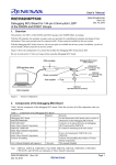
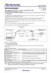
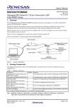
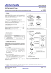
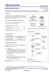
Figure 1 shows the configuration of a system that includes the debugging MCU board and an E20.
Be sure to read section 7, Notes on Usage, before using the debugging MCU board.
[*1] When using the debugging MCU board (R0E5562N8PFK10), the D/A converter function cannot be used.
Figure 1
2.
System Configuration
Components of the Debugging MCU Board
Table 1 lists the components of the debugging MCU board. Check that you have all of the components when you
unpack the box.
Table 1 Components of the Debugging MCU Board
Component
Quantity
1
Debugging MCU board
(R0E5562N8PFK10)
1
YQPACK100SD
(from Tokyo Eletech Corporation)
1
NQPACK100SD-ND
(from Tokyo Eletech Corporation)
4
YQ-GUIDE-S1
(from Tokyo Eletech Corporation)
1
Cautions in handling
User’s Manual (English and Japanese)
1 for each
Remarks
For the dimensions of the board, refer to section 6,
Dimensions of the Debugging MCU Board.
Connector to be placed between the debugging
MCU board and the NQPACK.
IC socket for mounting on the user system
Screws for fastening the YQPACK to the
NQPACK.
Cautions when handling the products of Tokyo
Eletech Corporation
This manual (English)
Note: NQPACK, YQPACK, YQSOCKET, YQ-GUIDE, HQPACK, TQPACK, TQSOCKET, CSSOCKET,
CSPLUG/W, and LSPACK are trademarks of Tokyo Eletech Corporation.
R20UT0217EJ0100 Rev.1.00
Dec 16, 2010
Page 1
R0E5562N8PFK10
3.
User's Manual
Specifications
Table 2 shows the functional specifications of the debugging MCU board.
Table 2 Specifications of the Debugging MCU Board
Item
Specification
MCU for use
• RX62N- and RX621-group MCUs in PLQP0100KB-A packages*1
The MCU type name
• R5F562N8BDBG
installed on the debugging
(ROM: 512 Kbytes, RAM: 96 Kbytes, Data flash: 32 Kbytes )
MCU board
Power supply
• Power(VCC = AVCC) at 2.7*2 to 3.6 V is supplied from the user system.
• The state of power supply can be monitored through the test pins (TP1 for
VCC and TP2 for GND).
•The state of analog power supply can be monitored through the test pin
(TP3 for VREFH).
System clock (EXTAL)
• This clock signal at 8 to 14 MHz is supplied from the user system.
Sub-clock (XCIN)
• The clock signal at 32.768 kHz is supplied from the user system.
Notes*:1. When using the debugging MCU board (R0E5562N8PFK10), the D/A converter function cannot be used.
Notes*:2. Please use it by voltage (VCC > VPOR) that doesn't enter the state of power on reset.
4.
Reset Circuit
Figure 2 shows the reset circuit, with the level on the RES# pin pulled up by a 510-kΩ resistor.
Figure 2
Reset Circuit on the Debugging MCU Board
R20UT0217EJ0100 Rev.1.00
Dec 16, 2010
Page 2
R0E5562N8PFK10
5.
User's Manual
Connection
To connect the debugging MCU board and user system,
follow the procedure below.
The R0E5562N8PFK10 can be used for debugging and
on-board evaluation in common by mounting the
NQPACK100SD-ND on the user system.
(1) For debugging
1. Mount the NQPACK100SD-ND on the user system.
Be sure to check that the location of pin 1 is correct.
2. Install the YQPACK100SD after checking for a match with
the position of pin 1 for the NQPACK100SD-ND.
Then use the YQ-GUIDE-S1 to affix the YQPACK100SD
to the NQPACK100SD-ND.
● Do NOT use the screws included with the
YQPACK100SD for fixing the YQPACK100SD.
● Do NOT use the screwdriver included with the
NQPACK100SD-ND for fixing the
YQ-GUIDE-S1. That is used only for the
HQPACK100SD. Note that you need to provide
your own screwdriver.
3. Connect the R0E5562N8PFK10 after checking for a match
with the position of pin 1 for the YQPACK100SD.
4. Install the connector of the flexible cable from the emulator
to the 38-pin connector on the R0E5562N8PFK10.
Hold the R0E5562N8PFK10 while connecting the cable to
avoid imposing heavy pressure on the 38-pin connector of
the R0E5562N8PFK10.
(2) For on-board evaluation
5. Mount an MCU with on-chip flash memory and the
HQPACK100SD (not included) in order on the
NQPACK100SD-ND on the user system.
(1) For debugging
Flexible cable
38-pin
connector
4
Pin 1
R0E5562N8PFK10
(back side:
YQSOCKET100SDF)
(2) For on-board evaluation
Use a flat-bladed
screwdriver.
3
YQ-GUIDE-S1(× 4)
HQPACK100SD
(not included)
YQPACK100SD
2
NQPACK100SD-ND
1
100-pin,0.5-mm pitch
(PLQP0100KB-A) pad pattern
MCU
5
indicates pin 1 in this example.
Check that the pin-1 positions on the pad pattern and
all of the components are correctly aligned.
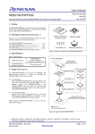
Figure 3
Board
Connection of the User System and the MCU
Before using the R0E5562N8PFK10, be sure to read
section 7, Notes on Usage.
WARNING
1. Always switch OFF the emulator, debugging MCU board, and user system before connecting or disconnecting the
emulator. Failure to do so will create a FIRE HAZARD and will damage the emulator, debugging MCU board, and
user system.
2. Make sure that the connectors on both ends of the user-system interface cable are facing the right way relative to the
user-side connector on the emulator and the 38-pin connector on the debugging MCU board, respectively. Incorrect
connection will create a FIRE HAZARD and will damage the emulator, debugging MCU board, and user system.
CAUTION
1. Check the locations of pin 1 before mounting the NQPACK.
2. The tightening torque must be no greater than 0.054 N•m. If the applied torque is not accurately measurable, stop
tightening when the force required to turn the screw (YQ-GUIDE-S1) becomes significantly greater than that
required at the start of tightening. Tightening a screw too much may break the screw hole of the NQPACK or lead
to a faulty connection by cracking solder on the NQPACK side.
3. Failure of conduction during operation may be due to a crack in the solder for the NQPACK. Check conduction
with a tester and re-solder the NQPACK as required.
R20UT0217EJ0100 Rev.1.00
Dec 16, 2010
Page 3
R0E5562N8PFK10
User's Manual
6. Dimensions of the Debugging MCU Board
Figures 4 shows the dimensions and reference pad pattern of the debugging MCU board (R0E5562N8PFK10).
Figure 4
Reference Pad Pattern and Dimensions of the Debugging MCU Board (R0E5562N8PFK10)
R20UT0217EJ0100 Rev.1.00
Dec 16, 2010
Page 4
R0E5562N8PFK10
7.
User's Manual
Notes on Usage
READ the following warnings before using the debugging MCU board. Incorrect operation will damage the debugging
MCU board and user system. The USER PROGRAM will be LOST.
Notes on Handling the Debugging MCU Board:
• Take full care not to touch any parts or cause short circuits on the debugging MCU board.
• Protect the debugging MCU board from excessive physical shock.
• Do not alter the debugging MCU board. If any alteration is attempted, the debugging MCU board will no
longer be supported.
• The MCU installed on the debugging MCU board is only for use in debugging. Do not remove the MCU
from the board to use it for other purposes.
• For purchasing the NQPACK100SD-ND, YQPACK100SD and HQPACK100SD, contact the following:
Tokyo Eletech Corporation http://www.tetc.co.jp/e_index.htm
Notes on Turning the Power On:
• Do not apply a power voltage that is beyond the range guaranteed for the MCU.
• Only supply power to the debugging MCU board and connected parts after having connecting all cables.
Notes on Connecting the Debugging MCU Board:
• Cables must not be connected or removed while the power is on.
• Before connecting the debugging MCU board and user system, check that the pin 1 locations on both
sides are correctly aligned with each other.
Notes on Rewriting the Flash Memory:
• The number of times that the flash memory in the MCU installed on the debugging MCU board can be
programmed is limited. If an error in erasure occurs during debugging, replace the debugging MCU
board.
Notes on Debugging:
• The debugging MCU board is only usable for debugging when it is connected to the user system.
• Debugging by the debugging MCU board alone is not supported.
Notes on Starting the Debugger and Selecting the MCU Type:
• Select the MCU type for use in the device name section of the [Initial Settings] dialog box on initiation of
the debugger.
Notes on Designing the User System:
• Pull the levels on the EMLE pin down to 4.7 kΩ to 10 kΩ.
• Pull the levels on the MD0 and MD1 pins up to 4.7 kΩ to 10 kΩ, and select the single-chip mode.
• Pull up or down the level on the MDE pin according to the endian used.
• The output of the reset circuit of the user system must be open collector.
Notes on the Flash Development Toolkit (FDT):
• Do not use the FDT when using the debugging MCU board.
Notes on the Writing the On-chip Flash Memory Mode:
• Do not use the writing the on-chip flash memory mode when using the debugging MCU board.
Notes on the D/A converter:
• When using the debugging MCU board, the D/A converter function cannot be used.
R20UT0217EJ0100 Rev.1.00
Dec 16, 2010
Page 5
R0E5562N8PFK10
User's Manual
Precautions
This product is only intended for use in a laboratory environment under ambient temperature and humidity
conditions. A safe separation distance should be used between this and any sensitive equipment. Its use outside the
laboratory, classroom, study area or similar such area invalidates conformity with the protection requirements of
the Electromagnetic Compatibility Directive and could lead to prosecution.
The product generates, uses, and can radiate radio frequency energy and may cause harmful interference to radio
communications. However, there is no guarantee that interference will not occur in a particular installation. If this
equipment causes harmful interference to radio or television reception, which can be determined by turning the
equipment off or on, you are encouraged to try to correct the interference by one or more of the following
measures;
• ensure attached cables do not lie across the equipment
• reorient the receiving antenna
• increase the distance between the equipment and the receiver
• connect the equipment into an outlet on a circuit different from that which the receiver is connected
• power down the equipment when not in use
• consult the dealer or an experienced radio/TV technician for help
NOTE: It is recommended that wherever possible shielded interface cables are used.
The product is potentially susceptible to certain EMC phenomena. To mitigate against them it is recommended that
the following measures be undertaken;
• The user is advised that mobile phones should not be used within 10m of the product when in use.
• The user is advised to take ESD precautions when handling the equipment.
This product does not represent an ideal reference design for an end product and does not fulfill the regulatory
standards for an end product.
R20UT0217EJ0100 Rev.1.00
Dec 16, 2010
Page 6
R0E5562N8PFK10
User's Manual
Regulatory Compliance Notices
European Union regulatory notices
This product complies with the following EU Directive. (This directive is only valid in the European Union.)
Environmental Compliance and Certifications:
x Restriction of the Use of Certain Hazardous Substances in Electrical and Electronic Equipment (RoHs)
Directive 2002/95/EC
x Waste Electrical and Electronic Equipment (WEEE) Directive 2002/96/EC
WEEE Marking Notice (European Union Only)
Renesas development tools and products are directly covered by the European
Union's Waste Electrical and Electronic Equipment, (WEEE), Directive
2002/96/EC. As a result, this equipment, including all accessories, must not be
disposed of as household waste but through your locally recognized recycling
or disposal schemes. As part of our commitment to environmental
responsibility Renesas also offers to take back the equipment and has
implemented a Tools Product Recycling Program for customers in Europe.
This allows you to return equipment to Renesas for disposal through our
approved Producer Compliance Scheme. To register for the program, click
here “http://www.renesas.com/weee".
8.
Warranty
1. The warranty of your product is valid for one year after purchase.
If your product becomes faulty or damaged while being used under good conditions by observing this user's manual,
we will repair or replace your faulty or damaged product free of charge.
2. Note, however, that if your product's fault or damage is raised by any one of the following causes, the warranty is
void.
a) Misuse, abuse, or use under extraordinary conditions
b) Improper handling such as dropping your product during transportation or carriage
c) Other connected equipments
d) Fires, earthquakes, lightning, flood and other unexpected disasters, damages and abnormal voltage.
e) Unauthorized remodeling, repair, adjustment, and so on
In the above cases, contact your local distributor.
If your product is being leased, consult the leasing company or the owner.
R20UT0217EJ0100 Rev.1.00
Dec 16, 2010
Page 7
Notice
1.
All information included in this document is current as of the date this document is issued. Such information, however, is subject to change without any prior notice. Before purchasing or
using any Renesas Electronics products listed herein, please confirm the latest product information with a Renesas Electronics sales office. Also, please pay regular and careful attention to
additional and different information to be disclosed by Renesas Electronics such as that disclosed through our website.
2. Renesas Electronics does not assume any liability for infringement of patents, copyrights, or other intellectual property rights of third parties by or arising from the use of Renesas
Electronics products or technical information described in this document. No license, express, implied or otherwise, is granted hereby under any patents, copyrights or other intellectual
property rights of Renesas Electronics or others.
3. You should not alter, modify, copy, or otherwise misappropriate any Renesas Electronics product, whether in whole or in part.
4. Descriptions of circuits, software and other related information in this document are provided only to illustrate the operation of semiconductor products and application examples. You are
fully responsible for the incorporation of these circuits, software, and information in the design of your equipment. Renesas Electronics assumes no responsibility for any losses incurred by
you or third parties arising from the use of these circuits, software, or information.
5. When exporting the products or technology described in this document, you should comply with the applicable export control laws and regulations and follow the procedures required by
such laws and regulations. You should not use Renesas Electronics products or the technology described in this document for any purpose relating to military applications or use by the
military, including but not limited to the development of weapons of mass destruction. Renesas Electronics products and technology may not be used for or incorporated into any products
or systems whose manufacture, use, or sale is prohibited under any applicable domestic or foreign laws or regulations.
6. Renesas Electronics has used reasonable care in preparing the information included in this document, but Renesas Electronics does not warrant that such information is error free.
Renesas Electronics assumes no liability whatsoever for any damages incurred by you resulting from errors in or omissions from the information included herein.
7. Renesas Electronics products are classified according to the following three quality grades: "Standard", "High Quality", and "Specific". The recommended applications for each Renesas
Electronics product depends on the product's quality grade, as indicated below. You must check the quality grade of each Renesas Electronics product before using it in a particular
application. You may not use any Renesas Electronics product for any application categorized as "Specific" without the prior written consent of Renesas Electronics. Further, you may not
use any Renesas Electronics product for any application for which it is not intended without the prior written consent of Renesas Electronics. Renesas Electronics shall not be in any way
liable for any damages or losses incurred by you or third parties arising from the use of any Renesas Electronics product for an application categorized as "Specific" or for which the
product is not intended where you have failed to obtain the prior written consent of Renesas Electronics. The quality grade of each Renesas Electronics product is "Standard" unless
otherwise expressly specified in a Renesas Electronics data sheets or data books, etc.
"Standard":
Computers; office equipment; communications equipment; test and measurement equipment; audio and visual equipment; home electronic appliances; machine tools;
personal electronic equipment; and industrial robots.
"High Quality": Transportation equipment (automobiles, trains, ships, etc.); traffic control systems; anti-disaster systems; anti-crime systems; safety equipment; and medical equipment
not specifically designed for life support.
"Specific":
Aircraft; aerospace equipment; submersible repeaters; nuclear reactor control systems; medical equipment or systems for life support (e.g. artificial life support devices or
systems), surgical implantations, or healthcare intervention (e.g. excision, etc.), and any other applications or purposes that pose a direct threat to human life.
8. You should use the Renesas Electronics products described in this document within the range specified by Renesas Electronics, especially with respect to the maximum rating, operating
supply voltage range, movement power voltage range, heat radiation characteristics, installation and other product characteristics. Renesas Electronics shall have no liability for
malfunctions or damages arising out of the use of Renesas Electronics products beyond such specified ranges.
9. Although Renesas Electronics endeavors to improve the quality and reliability of its products, semiconductor products have specific characteristics such as the occurrence of failure at a
certain rate and malfunctions under certain use conditions. Further, Renesas Electronics products are not subject to radiation resistance design. Please be sure to implement safety
measures to guard them against the possibility of physical injury, and injury or damage caused by fire in the event of the failure of a Renesas Electronics product, such as safety design for
hardware and software including but not limited to redundancy, fire control and malfunction prevention, appropriate treatment for aging degradation or any other appropriate measures.
Because the evaluation of microcomputer software alone is very difficult, please evaluate the safety of the final products or system manufactured by you.
10. Please contact a Renesas Electronics sales office for details as to environmental matters such as the environmental compatibility of each Renesas Electronics product. Please use
Renesas Electronics products in compliance with all applicable laws and regulations that regulate the inclusion or use of controlled substances, including without limitation, the EU RoHS
Directive. Renesas Electronics assumes no liability for damages or losses occurring as a result of your noncompliance with applicable laws and regulations.
11. This document may not be reproduced or duplicated, in any form, in whole or in part, without prior written consent of Renesas Electronics.
12. Please contact a Renesas Electronics sales office if you have any questions regarding the information contained in this document or Renesas Electronics products, or if you have any other
inquiries.
(Note 1) "Renesas Electronics" as used in this document means Renesas Electronics Corporation and also includes its majority-owned subsidiaries.
(Note 2) "Renesas Electronics product(s)" means any product developed or manufactured by or for Renesas Electronics.
http://www.renesas.com
SALES OFFICES
Refer to "http://www.renesas.com/" for the latest and detailed information.
Renesas Electronics America Inc.
2880 Scott Boulevard Santa Clara, CA 95050-2554, U.S.A.
Tel: +1-408-588-6000, Fax: +1-408-588-6130
Renesas Electronics Canada Limited
1101 Nicholson Road, Newmarket, Ontario L3Y 9C3, Canada
Tel: +1-905-898-5441, Fax: +1-905-898-3220
Renesas Electronics Europe Limited
Dukes Meadow, Millboard Road, Bourne End, Buckinghamshire, SL8 5FH, U.K
Tel: +44-1628-585-100, Fax: +44-1628-585-900
Renesas Electronics Europe GmbH
Arcadiastrasse 10, 40472 Düsseldorf, Germany
Tel: +49-211-65030, Fax: +49-211-6503-1327
Renesas Electronics (China) Co., Ltd.
7th Floor, Quantum Plaza, No.27 ZhiChunLu Haidian District, Beijing 100083, P.R.China
Tel: +86-10-8235-1155, Fax: +86-10-8235-7679
Renesas Electronics (Shanghai) Co., Ltd.
Unit 204, 205, AZIA Center, No.1233 Lujiazui Ring Rd., Pudong District, Shanghai 200120, China
Tel: +86-21-5877-1818, Fax: +86-21-6887-7858 / -7898
Renesas Electronics Hong Kong Limited
Unit 1601-1613, 16/F., Tower 2, Grand Century Place, 193 Prince Edward Road West, Mongkok, Kowloon, Hong Kong
Tel: +852-2886-9318, Fax: +852 2886-9022/9044
Renesas Electronics Taiwan Co., Ltd.
7F, No. 363 Fu Shing North Road Taipei, Taiwan
Tel: +886-2-8175-9600, Fax: +886 2-8175-9670
Renesas Electronics Singapore Pte. Ltd.
1 harbourFront Avenue, #06-10, keppel Bay Tower, Singapore 098632
Tel: +65-6213-0200, Fax: +65-6278-8001
Renesas Electronics Malaysia Sdn.Bhd.
Unit 906, Block B, Menara Amcorp, Amcorp Trade Centre, No. 18, Jln Persiaran Barat, 46050 Petaling Jaya, Selangor Darul Ehsan, Malaysia
Tel: +60-3-7955-9390, Fax: +60-3-7955-9510
Renesas Electronics Korea Co., Ltd.
11F., Samik Lavied' or Bldg., 720-2 Yeoksam-Dong, Kangnam-Ku, Seoul 135-080, Korea
Tel: +82-2-558-3737, Fax: +82-2-558-5141
If the requirements shown in the "CAUTION"
sentences are ignored, the equipment may cause
personal injury or damage to the products.
Renesas Tools Website http://www.renesas.com/tools
All trademarks and registered trademarks are the property
of their respective owners.
© 2010 Renesas Electronics Corporation and Renesas Solutions Corp. All rights reserved.
Colophon 1.0