1
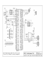
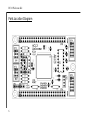
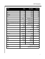
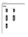
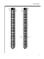
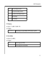
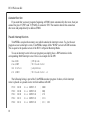
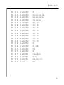
Hardware Version 1.0
Monitor Version 1.2
English Release
October 7 1999
HC12 Welcome Kit
Copyright (C)1996-98 by
MCT Elektronikladen GbR
Hohe Str. 9-13 D-04107 Leipzig
Telefon: +49-(0)341-2118354
Fax: +49-(0)341-2118355
mailto:[email protected]
http://www.elektronikladen.de/mct
This manual and the product described herein were designed carefully by the manufacturer. We made every
effort to avoid mistakes but we do not guarantee that it is 100% free of errors.
The manufacturers entire liability and your exclusive remedy shall be, at the manufacturers option, return of
the price paid or repair or replacement of the product. The manufacturer disclaims all other warranties, either
expressed or implied, including but not limited to implied warranties of merchantability and fitness for a
particular purpose, with respect to the product including accompanying written material, hardware and firmware.
In no event shall the manufacturer or its supplier be liable for any damages whatsoever (including, without
limitation, damages for loss of business profits, business interruption, loss of business information, or other
pecuniary loss) arising out of the use of or inability to use the product, even if the manufacturer has been advised
of the possibility of such damages. The product is not designed, intended or authorized for use in applications in
which the failure of the product could create a situation where personal injury or death may occur. Should you
use the product for any such unintended or unauthorized application, you shall indemnify and hold the
manufacturer and its suppliers harmless against all claims, even if such claim alleges that the manufacturer was
negligent regarding the design or implementation of the product.
Product features and prices may change without notice.
All trademarks are properties of their respective holders.
HC12 Welcome Kit
Contents
Technical Support
Schematic
Parts Location Diagram
Connectors
Jumpers
Memory Map
Technical Data
TwinPEEKs Monitor
2
3
6
8
10
11
12
13
1
HC12 Welcome Kit
Technical Support
To receive technical support please contact your local Elektronikladen dealer.
You may also send email to the Elektronikladen support team via the following email address:
[email protected]
2
HC12 Welcome Kit
Schematic
The main component on the HC12 Welcome Kit board is an 68HC812A4 microcontroller (U1)
from Motorola. The MCU is accompanied by a reset chip (low voltage inhibitor, U2) to avoid
problems whenever the voltage is below operating level. This device generates a reset if the voltage is
below 2.8V. The threshold level is set so low in order to operate the kit both with 5 and 3 volts. Please
note: We recommend to operate the HC12 with 5V, since Motorola deleted the 3V specification in
newer issues of the HC812A4 Technical Data documents. The RS232 level converter (U3) was
selected accordingly, it works at both voltages too.
The MCU generates its clocks from a 16 MHz crystal connected to the XTAL and EXTAL pins.
The HC12 also has a PLL which is not used here. If you would like to use the PLL feature, you must
replace the crystal and add the components C4, C5 and R6. Motorola has an application note about
how to choose the appropriate values.
All controller signals (except XTAL and XFC) are available via two double row header
connectors (ST5, ST6). The connectors are not mounted as factory default to allow you to solder them
up- or downward, depending on your application.
The jumpers JP1, JP2 and JP3 select the operating mode of the MCU. See section "Jumpers" for
details. JP4 is not really a jumper but a connector for an external reset switch.
BR1 and BR2 are solder pads on the solder side of the PCB. They are closed by default. You
may open them if you want to supply VDDA and/or VRH voltages different from VCC to the ADC
subsystem.
ST1 is a Motorola compliant 6 pin header for the BDM interface of the HC12. You may use it to
connect a BDM pod while debugging a program.
There is another 6 pin header (ST2) which is an optional BDM output. Presently ST2 has no
3
HC12 Welcome Kit
specific function on the HC12 Welcome Kit apart from the fact that it carries two general purpose I/O
port pins of the MCU.
The I/O pins of the HC812A4 have internal pull-up resistors, so there shouldn't be problems
leaving these pins unterminated.
4
HC12 Welcome Kit
5
HC12 Welcome Kit
Parts Location Diagram
6
HC12 Welcome Kit
Part No.
Value
Description
Comment
10M
Resistor
axial
47
Resistor
axial
R3,R7,R8,R9
4,7k
Resistor
axial
R5,R10
22k
Resistor
axial
47µF / 10V
Electrolytic Capacitor
0.1"
18pF
Ceramic Capacitor
0.1"
100nF
Ceramic Capacitor
0.1"
R1
R2,R4
C1
C2,C3
C6, C10, C11, C1A, C1B, C1C, C1D, C1E, C1F
1µF / 25V
Electrolytic Capacitor
0.1"
Q1
C7,C8,C9
16MHz
Crystal
HC49U/4
U1
68HC812A4
MCU
TQFP112
U2
MC34164P3
Reset Chip
TO92
U3
MAX3232CPE
RS232 Transceiver
DIP16
JP1,JP2,JP3
Header1x3
Jumper
JP4
Header1x2
Jumper
ST1,ST2
Header2x3
Header 6p.
ST3,ST4
Header2x5
Header 10p.
ST5,ST6
PF2x25
Header 50p.
SV_F35M
Power Supply Connector
ST7
BR1,BR2
Solder pads (on solder side of PCB)
C4,C5,R6
Optional parts for the PLL (not used here)
7
HC12 Welcome Kit
Connectors
BDM interface (Input)
BKGD
1
2
GND
n.c.
3
4
n.c.
5
6
BDM Out (optional)
BKGD_OUT
1
2
GND
/RESET
n.c.
3
4
/RES_OUT
VCC
n.c.
5
6
VCC
ST1
ST2
RS232 #0
RS232 #1
n.c.
1
2
n.c.
n.c.
1
2
n.c.
TX0
3
4
n.c.
TX1
3
4
n.c.
RX0
5
6
n.c.
RX1
5
6
n.c.
n.c.
7
8
n.c.
n.c.
7
8
n.c.
GND
9
10
n.c.
GND
9
10
n.c.
ST3
Power Supply
VCC
1
GND
2
n.c.
3
n.c.
4
ST7
8
ST4
HC12 Welcome Kit
ECLK/PE4
1
2
EXTAL
/RESET
1
2
LSTRB/PE3
MODB/PE6
3
4
MODA/PE5
RW/PE2
3
4
IRQ/PE1
PB0
5
6
ARST/PE7
XIRQ/PE0
5
6
PC7
PB2
7
8
PB1
PC6
7
8
PC5
PB4
9
10
PB3
PC4
9
10
PC3
PB6
11
12
PB5
PC2
11
12
PC1
PA0
13
14
PB7
PC0
13
14
PD7
PA2
15
16
PA1
PD6
15
16
PD5
PA4
17
18
PA3
PD4
17
18
PD3
PA6
19
20
PA5
PD2
19
20
PD1
PF0
21
22
PA7
PD0
21
22
BKGD
PF2
23
24
PF1
PG5
23
24
PG4
PF4
25
26
PF3
PG3
25
26
PG2
PF6
27
28
PF5
PG1
27
28
PG0
PH1
29
30
PH0
PJ7
29
30
PJ6
PH3
31
32
PH2
PJ5
31
32
PJ4
PH5
33
34
PH4
PJ3
33
34
PJ2
PH7
35
36
PH6
PJ1
35
36
PJ0
PAD0
37
38
VRH
PT7/BKGD_OUT
37
38
PT6/RES_OUT
PAD2
39
40
PAD1
PT5
39
40
PT4
PAD4
41
42
PAD3
PT3
41
42
PT2
PAD6
43
44
PAD5
PT1
43
44
PT0
VDDA
45
46
PAD7
PS7
45
46
PS6
TXD0
47
48
RXD0
PS5
47
48
PS4
GND
49
50
VCC
TXD1
49
50
RXD1
ST6
ST5
9
HC12 Welcome Kit
Jumpers
1
MODA
MODB
JP1
JP2
2
3
1
2
BKGD
JP3
3
1
2
Operating Mode
3
Special Single Chip
Special Expanded Narrow
Special Peripheral
Special Expanded Wide
Normal Single Chip (Factory Default)
Normal Expanded Narrow
Reserved (Forced to Peripheral)
Normal Expanded Wide
10
HC12 Welcome Kit
Memory Map
Single Chip Mode:
Memory Area
$0000 - $01FF
Resource
Registers
(relocatable in 2KB steps)
$0800 - $0BFF
RAM
(relocatable in 2KB steps)
$F000 - $FFFF
EEPROM
Expanded Mode:
Memory Area
$0000 - $01FF
Resource
Register
(relocatable in 2KB steps)
$0800 - $0BFF
RAM
(relocatable in 2KB steps)
$1000 - $1FFF
EEPROM
(relocatable in 4KB steps)
11
HC12 Welcome Kit
Technical Data
MCU 68HC812A4
16 MHz crystal clock (8 MHz interner clock)
1024 bytes RAM
4096 bytes EEPROM
8 channel 16 bit Timer
16 Bit Pulse Accumulator
Watchdog and Clock Monitor
2 x SCI, 1 x SPI
8 channel 8 bit A/D Converter
up to 24 Key Wakeup Ports
112 pin TQFP package
Dimensions
86 mm x 54 mm / 3.4" x 2.1"
Power Supply
4.5 ... 5.5 V operating voltage
Typical current consumption: 25mA
12
HC12 Welcome Kit
TwinPEEKs Monitor
Software Version 1.2
Overview
Every HC12 Welcome Kit contains the TwinPEEKs software monitor. TwinPEEKs starts
automatically if you set the operating mode of the MCU to Normal Single Chip Mode.
TwinPEEKs occupies the upper half of the internal EEPROM space (2KB out of 4KB) and 256
Bytes RAM (so the first 768 Bytes are free). The monitor protects itself from being deleted after every
reset. You will need a seperate BDM-Downloader to replace the monitor software.
To communicate with a Host-PC use the first RS232 channel (SCI0) of the HC12 Welcome Kit
and set your PC terminal program to 9600 Baud, 8N1, no handshake.
All memory writes to the user EEPROM area (the lower 2 KB) will be handled by the monitor
automatically.
Monitor Commands
Monitor commands start with a single character (for the specific command) and one or more
hexadecimal parameters seperated by a whitespace or comma. The address range of the MCU is
64KB, so addresses are up to 4 (hex) digits long. Ending addresses are in the form "Last address +1".
The Example displays the memory contents from $F100 to $F1FF:
D F100 F200
13
HC12 Welcome Kit
D: Dump Memory
Syntax: D [<AADR> [<EADR>]]
Examples:
d f000 f800
Display memory from $F000 to $F7FF.
d f000
Display memory from $F000. Stop $0100 Bytes after starting address.
d
Display the next $0100 Bytes.
E: Edit Memory
Syntax: E [<AADR>]
Examples:
e f000
Edit memory from $F000
e
Edit memory (use last ending address)
In Edit Mode you can change a byte or use one of the following commands:
14
HC12 Welcome Kit
<ENTER>
Go to next memory location.
-
Go to previous memory location.
=
Re-read the current memory location.
.
Quit Edit Mode
Q
Quit Edit Mode
F: Fill Memory
Syntax: F <AADR> <EADR> <BY>
Examples:
f f000 f800 ff
Fill the memory area from $F000 to $F7FF with the value $FF
G: Goto Address
Syntax: G [<AADR>]
Examples:
g f100
Call user program at $F100
g
Call user program at current address
15
HC12 Welcome Kit
H: Help
Syntax: H
Examples:
h
Display help message
L: Load S-Records
Syntax: L [<OFFS>]
Examples:
l
Load S-Record file into memory
l e000
Load S-Record file into memory and relocate all adresses in the S-Record file by the offset $E000
Usage: First type in the load command. The monitor displays the message "Loading...". Now you
can send the S-Record file using the ASCII upload function of your terminal program.
The monitor does not echo the characters received. The function aborts if a write error occurs.
The user may interrupt the function by pressing <ESC>.
The monitor can process S0, S1 and S9 type records.
Please take care when writing to EEPROM locations: Every write access can take up to 20ms
(10ms erase time + 10ms write time). TwinPEEKs handles EEPROM write accesses, but the user
must not send the data faster than it can be written.
The easiest way to ensure the correct download timing is to use a line-by-line transmission. For
16
HC12 Welcome Kit
this purpose, the monitor sends an acknowledge character "*" after each S-Record line, that was
processed. Setup your PC terminal program in a way that it waits for this handshake character. This
option is available in most terminal programs - even the TERMINAL.EXE application from Windows
3.1. has such an option.
Another way to avoid timing problems is to load your code with full speed into RAM and then
move it into EEPROM. Here comes an example: Your code occupies $F000..$F200. First load it into
the RAM area $0800..$0A00 using the load command with an offset of $1800: "L 1800". Then you
can move your program to the final (EEPROM) destination with: "M 0800 0A00 F000".
M: Move Memory
Syntax: M <AADR> <EADR> <ADR2>
Examples:
m 1000 1800 f000
Copy the contents of memory from $1000...$17FF to $F000 (...$F7FF)
17
HC12 Welcome Kit
Autostart function
If you want that your user program (beginning at $F000) starts automatically after reset, then just
connect the pins 35 (PH7) and 37 (PAD0) of connector ST6! The monitor detects this connection
after reset and jumps directly to address $F000.
Pseudo Interrupt Vectors
TwinPEEKs occupies the memory area which contains the interrupt vectors. To give the user
program access to interrupt vectors, TwinPEEKs remaps all the "ROM"-vectors to RAM locations.
This is equal to the pseudo vectors of the HC11 in Special Bootstrap Mode.
To use an interrupt vector in the user program you simply place a JMP instruction in the
corresponding RAM interrupt vector. Here is an example for the SPI:
ldaa
staa
ldd
std
#$06
$0BC7
#isrFunc
$0BC8
;
;
;
;
JMP Opcode
SPI Pseudo Vector
Jump Address
SPI Pseudo Vector + 1
The following listing is part of the TwinPEEKs monitor program. It shows, which interrupt
vector is placed as a pseudo vector at which address in RAM:
FFCE
FFD0
FFD2
FFD4
FFD6
18
:
:
:
:
:
0B
0B
0B
0B
0B
B8
BB
BE
C1
C4
dc.w
dc.w
dc.w
dc.w
dc.w
RAMTOP-72
RAMTOP-69
RAMTOP-66
RAMTOP-63
RAMTOP-60
;
;
;
;
;
KWUH
KWUJ
ATD
SCI1
SCI / SCI0
HC12 Welcome Kit
FFD8
FFDA
FFDC
FFDE
FFE0
FFE2
FFE4
FFE6
FFE8
FFEA
FFEC
FFEE
FFF0
FFF2
FFF4
FFF6
FFF8
FFFA
FFFC
FFFE
:
:
:
:
:
:
:
:
:
:
:
:
:
:
:
:
:
:
:
:
0B
0B
0B
0B
0B
0B
0B
0B
0B
0B
0B
0B
0B
0B
0B
0B
0B
0B
0B
F8
C7
CA
CD
D0
D3
D6
D9
DC
DF
E2
E5
E8
EB
EE
F1
F4
F7
FA
FD
00
dc.w
dc.w
dc.w
dc.w
dc.w
dc.w
dc.w
dc.w
dc.w
dc.w
dc.w
dc.w
dc.w
dc.w
dc.w
dc.w
dc.w
dc.w
dc.w
dc.w
RAMTOP-57
RAMTOP-54
RAMTOP-51
RAMTOP-48
RAMTOP-45
RAMTOP-42
RAMTOP-39
RAMTOP-36
RAMTOP-33
RAMTOP-30
RAMTOP-27
RAMTOP-24
RAMTOP-21
RAMTOP-18
RAMTOP-15
RAMTOP-12
RAMTOP-9
RAMTOP-6
RAMTOP-3
main
;
;
;
;
;
;
;
;
;
;
;
;
;
;
;
;
;
;
;
;
SPI
Pulse Accu Input Edge
Pulse Accu Overflow
Timer Overflow
TOC5 / TC7
TOC4 / TC6
TOC3 / TC5
TOC2 / TC4
TOC1 / TC3
TIC3 / TC2
TIC2 / TC1
TIC1 / TC0
RTI
IRQ / KWUD
XIRQ
SWI
Illegal Opcode
COP Fail
Clock Monitor Fail
Reset
19
HC12 Welcome Kit
Memory Usage
20
First
Last
Memory
Usage
$0800
$0AFF
RAM
== Available for user program ==
$0B00
$0BB7
RAM
Monitor Variables and Stack
$0BB8
$0BFF
RAM
Redirected Interrupt Vectors
$F000
$F7FF
EEPROM == Available for user program ==
$F800
$FFFF
EEPROM TwinPEEKs Monitor Code