1
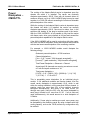
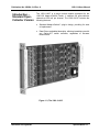
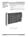
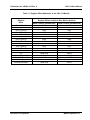
RACAL INSTRUMENTS™ 1260-114 HIGH DENSITY DIGITAL I/O PLUG-IN Publication No. 980824-114 Rev. A Astronics Test Systems Inc. 4 Goodyear, Irvine, CA 92618 Tel: (800) 722-2528, (949) 859-8999; Fax: (949) 859-7139 [email protected] [email protected] [email protected] http://www.astronicstestsystems.com Copyright 1998 by Astronics Test Systems Inc. Printed in the United States of America. All rights reserved. This book or parts thereof may not be reproduced in any form without written permission of the publisher. THANK YOU FOR PURCHASING THIS ASTRONICS TEST SYSTEMS PRODUCT For this product, or any other Astronics Test Systems product that incorporates software drivers, you may access our web site to verify and/or download the latest driver versions. The web address for driver downloads is: http://www.astronicstestsystems.com/support/downloads If you have any questions about software driver downloads or our privacy policy, please contact us at: [email protected] WARRANTY STATEMENT All Astronics Test Systems products are designed to exacting standards and manufactured in full compliance to our AS9100 Quality Management System processes. This warranty does not apply to defects resulting from any modification(s) of any product or part without Astronics Test Systems express written consent, or misuse of any product or part. The warranty also does not apply to fuses, software, non-rechargeable batteries, damage from battery leakage, or problems arising from normal wear, such as mechanical relay life, or failure to follow instructions. This warranty is in lieu of all other warranties, expressed or implied, including any implied warranty of merchantability or fitness for a particular use. The remedies provided herein are buyer’s sole and exclusive remedies. For the specific terms of your standard warranty, contact Customer Support. Please have the following information available to facilitate service. 1. Product serial number 2. Product model number 3. Your company and contact information You may contact Customer Support by: E-Mail: [email protected] Telephone: +1 800 722 3262 (USA) Fax: +1 949 859 7139 (USA) RETURN OF PRODUCT Authorization is required from Astronics Test Systems before you send us your product or sub-assembly for service or calibration. Call or contact Customer Support at 1-800-722-3262 or 1-949-859-8999 or via fax at 1949-859-7139. We can also be reached at: [email protected]. If the original packing material is unavailable, ship the product or sub-assembly in an ESD shielding bag and use appropriate packing materials to surround and protect the product. PROPRIETARY NOTICE This document and the technical data herein disclosed, are proprietary to Astronics Test Systems, and shall not, without express written permission of Astronics Test Systems, be used in whole or in part to solicit quotations from a competitive source or used for manufacture by anyone other than Astronics Test Systems. The information herein has been developed at private expense, and may only be used for operation and maintenance reference purposes or for purposes of engineering evaluation and incorporation into technical specifications and other documents which specify procurement of products from Astronics Test Systems. TRADEMARKS AND SERVICE MARKS All trademarks and service marks used in this document are the property of their respective owners. • Racal Instruments, Talon Instruments, Trig-Tek, ActivATE, Adapt-A-Switch, N-GEN, and PAWS are trademarks of Astronics Test Systems in the United States. DISCLAIMER Buyer acknowledges and agrees that it is responsible for the operation of the goods purchased and should ensure that they are used properly and in accordance with this document and any other instructions provided by Seller. Astronics Test Systems products are not specifically designed, manufactured or intended to be used as parts, assemblies or components in planning, construction, maintenance or operation of a nuclear facility, or in life support or safety critical applications in which the failure of the Astronics Test Systems product could create a situation where personal injury or death could occur. Should Buyer purchase Astronics Test Systems product for such unintended application, Buyer shall indemnify and hold Astronics Test Systems, its officers, employees, subsidiaries, affiliates and distributors harmless against all claims arising out of a claim for personal injury or death associated with such unintended use. FOR YOUR SAFETY Before undertaking any troubleshooting, maintenance or exploratory procedure, read carefully the WARNINGS and CAUTION notices. This equipment contains voltage hazardous to human life and safety, and is capable of inflicting personal injury. If this instrument is to be powered from the AC line (mains) through an autotransformer, ensure the common connector is connected to the neutral (earth pole) of the power supply. Before operating the unit, ensure the conductor (green wire) is connected to the ground (earth) conductor of the power outlet. Do not use a two-conductor extension cord or a three-prong/two-prong adapter. This will defeat the protective feature of the third conductor in the power cord. Maintenance and calibration procedures sometimes call for operation of the unit with power applied and protective covers removed. Read the procedures and heed warnings to avoid “live” circuit points. Before operating this instrument: 1. Ensure the proper fuse is in place for the power source to operate. 2. Ensure all other devices connected to or in proximity to this instrument are properly grounded or connected to the protective third-wire earth ground. If the instrument: - fails to operate satisfactorily shows visible damage has been stored under unfavorable conditions has sustained stress Do not operate until performance is checked by qualified personnel. This page was left intentionally blank. Publication No. 980824-114 Rev. A 1260-114 User Manual Table of Contents Chapter 1 ............................................................................................................................ 1-1 SPECIFICATIONS ........................................................................................................................ 1-1 Introduction – TTL Version ........................................................................................................ 1-1 Specifications – TTL .................................................................................................................. 1-2 Power Dissipation – TTL ........................................................................................................... 1-3 Introduction – CMOS/TTL Version............................................................................................. 1-4 Specifications – CMOS/TTL ...................................................................................................... 1-5 Power Dissipation – CMOS/TTL ................................................................................................ 1-6 Introduction – Standard Open-Collector Version ....................................................................... 1-7 Specifications – Standard Open Collector ................................................................................. 1-8 Power Dissipation – Standard Open-Collector ........................................................................... 1-9 Introduction – High Current/Voltage Open-Collector Version ................................................... 1-10 Specifications – High Current/Voltage Open-Collector ............................................................ 1-11 Power Dissipation – High Current/Voltage Open-Collector ...................................................... 1-12 About MTBF ............................................................................................................................ 1-13 Ordering Information ............................................................................................................... 1-13 Chapter 2 ............................................................................................................................ 2-1 INSTALLATION INSTRUCTIONS ................................................................................................. 2-1 Unpacking and Inspection ......................................................................................................... 2-1 Installation ................................................................................................................................. 2-1 Module Configuration ................................................................................................................ 2-2 Front Panel Connectors ......................................................................................................... 2-2 Astronics Test Systems i 1260-114 User Manual Publication No. 980824-114 Rev. A Mating Connectors................................................................................................................. 2-5 Chapter 3 ............................................................................................................................ 3-1 MODULE OPERATION ................................................................................................................ 3-1 Setting the Module Address ...................................................................................................... 3-1 Operating Modes....................................................................................................................... 3-2 Operating In Message-Based Mode .......................................................................................... 3-4 Port Descriptors For The 1260-114 ....................................................................................... 3-4 Reply To The MOD:LIST? Command .................................................................................... 3-5 Operating The 1260-114 in Register-Based Mode .................................................................... 3-5 1260-114 Example Code ..................................................................................................... 3-14 Chapter 4 ............................................................................................................................ 4-1 OPTIONAL ASSEMBLIES ............................................................................................................ 4-1 ii Astronics Test Systems Publication No. 980824-114 Rev. A 1260-114 User Manual List of Figures Figure 1-1, The 1260-114TTL ....................................................................................................... 1-1 Figure 1-2, The 1260-114CMOS ................................................................................................... 1-4 Figure 1-3, The 1260-114OC ........................................................................................................ 1-7 Figure 1-4, The 1260-114HVOC ................................................................................................. 1-10 Figure 2-1, Front-Panel Connector Pin Numbering ....................................................................... 2-3 Figure 2-2, Block Diagram ............................................................................................................ 2-5 Figure 3-1, Message-Based Mode of Operation ........................................................................... 3-3 Figure 3-2, Register-Based Mode of Operation............................................................................. 3-3 List of Tables Table 2-1, 1260-114 Front-Panel Connections ............................................................................. 2-4 Table 3-1, Register Offset Addresses of the 1260-114 Module ..................................................... 3-7 Table 3-2, ID Register Functionality of the 1260-114 .................................................................... 3-8 Table 3-3, Ports A-F Register Functionality of the 1260-114 Module ............................................ 3-8 Table 3-4, Ports G-L Register Functionality of the 1260-114 Module ............................................ 3-9 Table 3-5, Control Register 1 Functionality of the 1260-114 Module ........................................... 3-10 Table 3-6, Control Register 2 Functionality of the 1260-114 Module ........................................... 3-11 Table 3-7, Control Register 3 Functionality of the 1260-114 Module ........................................... 3-12 Table 3-8, EPROM Descriptor Functionality of the 1260-114 Module ......................................... 3-12 Astronics Test Systems iii 1260-114 User Manual Publication No. 980824-114 Rev. A This page was left intentionally blank. iv Astronics Test Systems Publication No. 980824-114 Rev. A 1260-114 User Manual DOCUMENT CHANGE HISTORY Revision Date A 02/10/09 No change 03/19/09 Astronics Test Systems Description of Change Revised per EO 29566 Revised format to current standards. Company name revised throughout manual. Manual now revision letter controlled. Added Document Change History Page v. Back of cover sheet. Revised Warranty Statement, Return of Product, Proprietary Notice and Disclaimer to current standards. Removed Reshipment Instructions in (Chap. 2-1) and removed (Chap 5). Information. Now appears in first 2 sheets behind cover sheet. Updated table of contents to reflect changes made. . v 1260-114 User Manual Publication No. 980824-114 Rev. A This page was left intentionally blank. vi Astronics Test Systems Publication No. 980824-114 Rev. A 1260-114 User Manual Chapter 1 SPECIFICATIONS Introduction – TTL Version The 1260-114TTL is a plug-in switch module developed for the 1260-100 Adapt-a-Switch Carrier. It switches 96 digital channels that are compliant to both level and current specifications for TTL logic. The 1260-114TTL includes the following features: • Standard Adapt-a-Switch plug-in design, providing for ease of replacement • Data-Driven embedded descriptor, allowing immediate use with any Option-01T switch controller, regardless of firmware revision level. Figure 1-1, The 1260-114TTL Astronics Test Systems Specifications 1-1 1260-114 User Manual Specifications – TTL Publication No. 980824-144 Rev. A Max. Chan. Input Voltage 5.5 VDC Chan. Output Current ±30 mA maximum Min. High Output Voltage ≥ 2 VDC @ -15 mA Max. Low Output Voltage ≤ 0.5 VDC @ 24 mA Available I/O Channels 96 Bi-directional I/O Channel Synchronization Asynchronous, Synchronous or Mixed Synchronous Trigger Handshake Polarity User Programmable Synchronous Busy Handshake Polarity User Programmable Shock 30g, 11 ms, ½ sine wave Vibration 0.013 in. P-P, 5-55 Hz Bench Handling 4 in., 45° Cooling See 1260-100 cooling data Temperature Operating Non-operating 0°C to +55°C -40°C to +75°C Relative Humidity Altitude Operating Non-operating Power Requirements +5 VDC Specifications 1-2 85% + 5% non-condensing at < 30°C 10,000 feet 15,000 feet 2.5 A maximum with all channels sourcing maximum current Weight 6 oz. (0.21 kg.) Mean Time Between Failures (MTBF) >100,000 hours (MIL-HDBK-217E) Mean Time to Repair < 5 minutes (MTTR) Astronics Test Systems Publication No. 980824-114 Rev. A Power Dissipation – TTL 1260-114 User Manual The cooling of the Adapt-a-Switch carrier is dependent upon the chassis into which it is installed. The carrier can nominally dissipate approximately 100 W. Even with all channels driven to maximum outputs, up to six 1260-114 TTL plug-ins may be used together in a 1260-100 without exceeding the maximum allowable power dissipation of the carrier. If the 1260-114TTL will be used in conjunction with other cards, the 1260-114TTL dissipation should be computed and summed with the total worst-case dissipation of the remaining modules. For example, a 1260-114TTL module would dissipate the following energy: Quiescent power dissipation = 4.25W maximum Channel dissipation = [(Vcc – 2.25) * current * 96(# channels energized)] + [(current)2 * (path resistance) * 96(# channels energized)] Total Power Dissipation = Quiescent + Channel Assuming all 96 channels are sourcing a maximum current of 30 mA and a path resistance of 1Ω: Total power dissipation = [(5 VDC - 2.25) * 0.030 A * 96] + [(0.030 A)2 * (1 Ω) * 96] + ( 4.25 W) = 12.25 W at 55°C This is acceptable power dissipation for an individual plug-in module. If five additional modules are likewise loaded, then the overall carrier dissipation is approximately 74 W, which is well within the cooling available in most commercial VXIbus chassis. In practice, rarely are more than 25% of the module’s channels energized simultaneously, and rarely is full rated current run through every path. Using the 25% rule, the power dissipated by each plug-in should be no more than 3 W. If all six slots are used simultaneously, this would amount to a total dissipation of 18Watts. Additionally, if fewer plug-in modules are used, more power may be dissipated by the remaining cards. By using a chassis with high cooling capacity, such as the 1261B, almost any configuration may be realized. Astronics Test Systems Specifications 1-3 1260-114 User Manual Introduction – CMOS/TTL Version Publication No. 980824-144 Rev. A The 1260-114CMOS is a plug-in switch module developed for the 1260-100 Adapt-a-Switch Carrier. It switches 96 digital channels that are compliant to both level and current specifications for CMOS. The 1260-114CMOS is also TTL-level compliant, but at a reduced sink and source current. For applications requiring TTLlevel compliance at higher currents, the 1260-114TTL should be selected The 1260-114CMOS includes the following features: • Standard Adapt-a-Switch plug-in design, providing for ease of replacement • Data-Driven embedded descriptor, allowing immediate use with any Option-01T switch controller, regardless of firmware revision level. Figure 1-2, The 1260-114CMOS Specifications 1-4 Astronics Test Systems Publication No. 980824-114 Rev. A Specifications – CMOS/TTL Max. Chan. Input Voltage 5.5 VDC Chan. Output Current ±8 mA maximum Min. High Output Voltage ≥ 3.8 VDC @ -8 mA Max. Low Output Voltage ≤ 0.44 VDC @ 8 mA Available I/O Channels 96 Bi-directional I/O Channel Synchronization Asynchronous, Synchronous or Mixed Synchronous Trigger Handshake Polarity User Programmable Synchronous Busy Handshake Polarity User Programmable Shock 30g, 11 ms, ½ sine wave Vibration 0.013 in. P-P, 5-55 Hz Bench Handling 4 in., 45° Cooling See 1260-100 cooling data Temperature Operating Non-operating 0°C to +55°C -40°C to +75°C Relative Humidity Altitude Operating Non-operating Power Requirements +5 VDC Astronics Test Systems 1260-114 User Manual 85% + 5% non-condensing at < 30°C 10,000 feet 15,000 feet 1 A maximum with all channels sourcing maximum loads Weight 6 oz. (0.21 kg.) Mean Time Between Failures (MTBF) >100,000 hours (MIL-HDBK-217E) Mean Time to Repair < 5 minutes (MTTR) Specifications 1-5 1260-114 User Manual Power Dissipation – CMOS/TTL Publication No. 980824-144 Rev. A The cooling of the Adapt-a-Switch carrier is dependent upon the chassis into which it is installed. The carrier can nominally dissipate approximately 100 W. Even with all channels driven to maximum outputs, up to six 1260-114CMOS plug-ins may be used together in a 1260-100 without exceeding the maximum allowable power dissipation of the carrier. While the cooling of the Adapt-a-Switch carrier is dependent upon the chassis into which it is installed, the carrier can normally dissipate approximately 100 W. Care must be taken, then, in the selection and loading of the plug-in modules used in the carrier. With the 1260-114CMOS it is not possible to fully load the carrier with these cards, drive every channel at full load and exceed the power dissipation capabilities of the Adapt-a-Switch carrier. If the 1260-114CMOS will be used in conjunction with other cards, the 1260-114CMOS dissipation should be computed and summed with the total worst-case dissipation of the remaining modules. For example, a 1260-114CMOS module would dissipate the following energy: Quiescent power dissipation = 0.75W maximum Channel dissipation = [(Vcc – 3.8) * current * 96(# channels energized)] + 2 [(current) * (path resistance) * 96(# channels energized)] Total Power Dissipation = Quiescent + Channel Assuming all 96 channels are sourcing a maximum current of 8 mA and a path resistance of 1Ω: Total power dissipation = 2 [(5 VDC – 3.8) * 0.008 A * 96] + [(0.008 A) * (1 Ω) * 96] + ( 0.75 W) = 1.7 W at 55°C This is acceptable power dissipation for an individual plug-in module. If five additional modules are likewise loaded, then the overall carrier dissipation is approximately 10 W, which is well within the cooling available in most commercial VXIbus chassis. In practice, rarely are more than 25% of the module’s channels energized simultaneously, and rarely is full rated current run through every path. Using the 25% rule, the power dissipated by each plug-in should be no more than 0.5 W. If all six slots are used simultaneously, this would amount to a total dissipation of 2.5Watts. Additionally, if fewer plug-in modules are used, more power may be dissipated by the remaining cards. By using a chassis with high cooling capacity, such as the 1261B, almost any configuration may be realized. Specifications 1-6 Astronics Test Systems Publication No. 980824-114 Rev. A Introduction – Standard OpenCollector Version 1260-114 User Manual The 1260-114OC is a plug-in switch module developed for the 1260-100 Adapt-a-Switch Carrier. It switches 96 open-collector channels at 200 mA per channel. The 1260-114OC includes the following features: • Standard Adapt-a-Switch plug-in design, providing for ease of replacement • Data-Driven embedded descriptor, allowing immediate use with any Option-01T switch controller, regardless of firmware revision level. Figure 1-3, The 1260-114OC Astronics Test Systems Specifications 1-7 1260-114 User Manual Specifications – Standard Open Collector Publication No. 980824-144 Rev. A Max. Chan. Input Voltage 32 VDC Chan. Output Current 200 mA maximum High Output Voltage 5 ≤ Voh ≤ 32 VDC Max. Low Output Voltage ≤ 1.5 VDC @ 200 mA Available I/O Channels 96 open-collector channels Channel Synchronization Asynchronous, Synchronous or Mixed Synchronous Trigger Handshake Polarity User Programmable Synchronous Busy Handshake Polarity User Programmable Shock 30g, 11 ms, ½ sine wave Vibration 0.013 in. P-P, 5-55 Hz Bench Handling 4 in., 45° Cooling See 1260-100 cooling data Temperature Operating Non-operating 0°C to +55°C -40°C to +75°C Relative Humidity Specifications 1-8 85% + 5% non-condensing at < 30°C Altitude Operating Non-operating 10,000 feet 15,000 feet Power Requirements +5 VDC 0.5 A maximum Weight 6 oz. (0.21 kg.) Mean Time Between Failures (MTBF) >100,000 hours (MIL-HDBK-217E) Mean Time to Repair < 5 minutes (MTTR) Astronics Test Systems Publication No. 980824-114 Rev. A Power Dissipation – Standard OpenCollector 1260-114 User Manual The cooling of the Adapt-a-Switch carrier is dependent upon the chassis into which it is installed. The carrier can nominally dissipate approximately 100 W. Even with all channels driven to maximum outputs, up to six 1260-114OC plug-ins may be used together in a 1260-100 without exceeding the maximum allowable power dissipation of the carrier. If the 1260-114OC will be used in conjunction with other cards, the 1260-114OC dissipation should be computed and summed with the total worst-case dissipation of the remaining modules. For example, a 1260-114OC module would dissipate the following energy: Quiescent power dissipation = 0.75W maximum Channel dissipation = [(Vol) * current * 96(# channels energized)] + [(current)2 * (path resistance) * 96(# channels energized)] Total Power Dissipation = Quiescent + Channel Assuming all 96 channels are sinking a maximum current of 200 mA and a path resistance of 0.5 Ω: Total power dissipation = [(1.5) * 0.200 A * 96] + [(0.200 A)2 * (0.5 Ω) * 96] + ( 0.75 W) = 31.5 W at 55°C This exceeds the acceptable power dissipation for an individual plug-in module. If five additional modules are likewise loaded, then the overall carrier dissipation is approximately 188 W, which is above the typical cooling capabilities of the carrier and most chassises in a two slot configuration. Therefore using a fully loaded Adapt-a-Switch carrier with these cards operating at the maximum extreme is not permissible. In practice, however, rarely are more than 25% of the module’s channels energized simultaneously, and rarely is full rated current run through every path. In addition, temperatures are typically not run at the rated maximum. Using the 25% rule, the power dissipated by each plugin should be no more than 8 W. If all six slots are used simultaneously, this would amount to a total dissipation of 48Watts. Additionally, if fewer plug-in modules are used, more power may be dissipated by the remaining cards. By using a chassis with high cooling capacity, such as the 1261B, almost any configuration may be realized. Astronics Test Systems Specifications 1-9 1260-114 User Manual Introduction – High Current/Voltage Open-Collector Version Publication No. 980824-144 Rev. A The 1260-114HVOC is a plug-in switch module developed for the 1260-100 Adapt-a-Switch Carrier. It switches 48 open-collector channels at 50V and 1.5 A per channel. The 1260-114HVOC includes the following features: • Standard Adapt-a-Switch plug-in design, providing for ease of replacement • Data-Driven embedded descriptor, allowing immediate use with any Option-01T switch controller, regardless of firmware revision level. Figure 1-4, The 1260-114HVOC Specifications 1-10 Astronics Test Systems Publication No. 980824-114 Rev. A Specifications – High Current/Voltage Open-Collector Max. Chan. Input Voltage 50 VDC Chan. Output Current 1.5 A maximum High Output Voltage 2 ≤ Voh ≤ 50 VDC Max. Low Output Voltage ≤ 0.5 VDC @ 1.5 A Available I/O Channels 48 open-collector channels Channel Synchronization Asynchronous, Synchronous or Mixed Synchronous Trigger Handshake Polarity User Programmable Synchronous Busy Handshake Polarity User Programmable Shock 30g, 11 ms, ½ sine wave Vibration 0.013 in. P-P, 5-55 Hz Bench Handling 4 in., 45° Cooling See 1260-100 cooling data Temperature Operating Non-operating 0°C to +55°C -40°C to +75°C Relative Humidity Astronics Test Systems 1260-114 User Manual 85% + 5% non-condensing at < 30°C Altitude Operating Non-operating 10,000 feet 15,000 feet Power Requirements +5 VDC 0.5 A maximum Weight 6 oz. (0.21 kg.) Mean Time Between Failures (MTBF) >100,000 hours (MIL-HDBK-217E) Mean Time to Repair < 5 minutes (MTTR) Specifications 1-11 1260-114 User Manual Power Dissipation – High Current/Voltage Open-Collector Publication No. 980824-144 Rev. A The cooling of the Adapt-a-Switch carrier is dependent upon the chassis into which it is installed. The carrier can nominally dissipate approximately 100 W. Even with all channels driven to maximum outputs, up to six 1260-114 TTLHVOC plug-ins may be used together in a 1260-100 without exceeding the maximum allowable power dissipation of the carrier. If the 1260-114HVOC will be used in conjunction with other cards, the 1260-114HVOC dissipation should be computed and summed with the total worst-case dissipation of the remaining modules. For example, a 1260-114HVOC module would dissipate the following energy: Quiescent power dissipation = 0.75W maximum Channel dissipation = [(Rds) * (current)2 * 48(# channels energized)] + [(current)2 * (path resistance) * 48(# channels energized)] Total Power Dissipation = Quiescent + Channel Assuming all 48 channels are sinking a maximum current of 1.5 A and a path resistance of 0.030 Ω: Total power dissipation = [(1.5 A)2 * (0.060 Ω) * 48]+ [(1.5 A)2 * (0.070 Ω) * 48] + ( 0.75 W) = 15 W at 55°C This is acceptable power dissipation for an individual plug-in module. If five additional modules are likewise loaded, then the overall carrier dissipation is approximately 89 W, which is well within the cooling available in most commercial VXIbus chassis. In practice, rarely are more than 25% of the module’s channels energized simultaneously, and rarely is full rated current run through every path. Using the 25% rule, the power dissipated by each plug-in should be no more than 3.75 W. If all six slots are used simultaneously, this would amount to a total dissipation of about 23Watts. Additionally, if fewer plug-in modules are used, more power may be dissipated by the remaining cards. By using a chassis with high cooling capacity, such as the 1261B, almost any configuration may be realized. Specifications 1-12 Astronics Test Systems Publication No. 980824-114 Rev. A 1260-114 User Manual About MTBF The 1260-114 MTBF is 783,668 hours, calculated in accordance with MIL-HDBK-217E. Ordering Information Listed below are part numbers for both the 1260-114 switch module and available mating connector accessories. Each 1260114 uses a single mating connector. ITEM DESCRIPTION PART # 1260-114TTL Switch Module Switch Module, 96-Channel TTL Digital Output Consists of: P/N 405145-001 PCB Assy P/N 980824-114 Manual 407661-001 1260-114CMOS Switch Module Switch Module, 96-Channel CMOS Digital Output 407661-002 Consists of: P/N 405145-002 PCB Assy P/N 980824-114 Manual 1260-114OC Switch Module Switch Module, 96-Channel Standard Open-Collector Output 407661-003 Consists of: P/N 405145-003 PCB Assy P/N 980824-114 Manual 1260-114HVOC Switch Module Switch Module, 48-Channel High Current/Voltage Open-Collector Output 407661-004 Consists of: P/N 405145-004 PCB Assy P/N 980824-114 Manual 160-pin Mating Connector 160 Pin Conn. Kit with pins 407664 Cable Assy. 6ft, Sleeved 160 Pin Cable Assy, 6 Ft, 24 AWG 407408-001 Connector Bracket Bracket, Strain Relief 456673 Additional Manual Astronics Test Systems 980824-114 Specifications 1-13 1260-114 User Manual Publication No. 980824-144 Rev. A This page was left intentionally blank. Specifications 1-14 Astronics Test Systems Publication No. 980824-114 Rev. A 1260-114 User Manual Chapter 2 INSTALLATION INSTRUCTIONS Unpacking and Inspection 1. Remove the 1260-114 module and inspect it for damage. If any damage is apparent, inform the carrier immediately. Retain shipping carton and packing material for the carrier’s inspection. 2. Verify that the pieces in the package you received contain the correct 1260-114 module option and the 1260-114 Users Manual. Notify Customer Support if the module appears damaged in any way. Do not attempt to install a damaged module into a VXI chassis. 1. The 1260-114 module is shipped in an anti-static bag to prevent electrostatic damage to the module. Do not remove the module from the anti-static bag unless it is in a staticcontrolled area. Installation Astronics Test Systems Installation of the 1260-114 Switching Module into a 1260-100 Carrier assembly is described in the Installation section of the 1260-100 Adapt-a-Switch Carrier Manual. Installation Instructions 2-1 1260-114 User Manual Publication No. 980824-114 Rev. A Module Configuration The 1260-114 is a 96-channel (48-channel for HVOC version), digital I/O plug-in for the Adapt-a-Switch Series. Its architecture permits any 8-bit port to be defined through software as in input or output in either asynchronous or synchronous operational mode. For the open-collector versions, the ports can be used as inputs by setting the transistors in an off state. Front Panel Connectors The 1260-114 has one 160-pin front-panel connector, labeled J200. It is a 160-pin, modified DIN style, with 0.025” square posts as pins. It has one pin for each input and one for each output. See Figure 2-1 for pin numbering. Table 2-1 shows the mapping of channel numbers to connector pins. Information about available mating connectors is provided immediately after Table 2-1. Installation Instructions 2-2 Astronics Test Systems Publication No. 980824-114 Rev. A 1260-114 User Manual a b c d e 32 31 30 29 28 27 26 25 24 23 22 21 20 19 18 17 16 15 14 13 12 11 10 9 8 7 6 5 4 3 2 1 Figure 2-1, Front-Panel Connector Pin Numbering Astronics Test Systems Installation Instructions 2-3 1260-114 User Manual Publication No. 980824-114 Rev. A Table 2-1, 1260-114 Front-Panel Connections Pin # 1 2 3 4 5 6 7 8 9 10 11 12 13 14 15 16 17 18 19 20 21 22 23 24 25 26 27 28 29 30 31 32 Row A A0 A1 A2 A3 A4 A5 A6 A7 B0 B1 B2 B3 B4 B5 B6 B7 G0 (GND) † G1 (GND) † G2 (GND) † G3 (GND) † G4 (GND) † G5 (GND) † G6 (GND) † G7 (GND) † H0 (GND) † H1 (GND) † H2 (GND) † H3 (GND) † H4 (GND) † H5 (GND) † H6 (GND) † H7 (GND) † Connector Pin Descriptions Row B Row C Row D C0 E0 Hi-Z (Fly) A ‡ C1 E1 GND C2 E2 GND C3 E3 GND C4 E4 Hi-Z (Fly) C ‡ C5 E5 GND C6 E6 GND C7 E7 GND D0 F0 Hi-Z (Fly) E ‡ D1 F1 GND D2 F2 GND D3 F3 GND D4 F4 Hi-Z (Fly) G ‡ D5 F5 GND D6 F6 GND D7 F7 GND I0 (GND) † K0 (GND) † Hi-Z (Fly) I ‡ I1 (GND) † K1 (GND) † GND I2 (GND) † K2 (GND) † GND I3 (GND) † K3 (GND) † GND I4 (GND) † K4 (GND) † Hi-Z (Fly) K ‡ I5 (GND) † K5 (GND) † GND I6 (GND) † K6 (GND) † GND I7 (GND) † K7 (GND) † GND J0 (GND) † L0 (GND) † EXTBUSY J1 (GND) † L1 (GND) † GND J2 (GND) † L2 (GND) † GND J3 (GND) † L3 (GND) † GND J4 (GND) † L4 (GND) † GND J5 (GND) † L5 (GND) † GND J6 (GND) † L6 (GND) † GND J7 (GND) † L7 (GND) † GND Row E Hi-Z (Fly) B ‡ GND GND GND Hi-Z (Fly) D ‡ GND GND GND Hi-Z (Fly) F ‡ GND GND GND Hi-Z (Fly) H ‡ GND GND GND Hi-Z (Fly) J ‡ GND GND GND Hi-Z (Fly) L ‡ GND GND GND EXTCLKIN GND GND GND GND GND GND GND † For the 1260-114HVOC version these pins are tied to ground. ‡ For the 1260-114TTL and 1260-114CMOS, these pins act as external tri-state inputs (active low) for the indicated ports. For the 1260-114OC and 1260-114HVOC, these pins connect to the fly-back protection diodes assigned to the indicated ports. Pins for Ports G-L are not connected in the 1260-114HVOC version. Installation Instructions 2-4 Astronics Test Systems Publication No. 980824-114 Rev. A 48 Chans Vcc 96 Chans Channel I/O Readback 1260-114 User Manual Vcc Readback External Flyback / Tri-State Control External Flyback / Tri-State Control Internal Tri-State 96 Chans Channel I/O Vcc Internal Tri-State Gnd -114HVOC -114OC Gnd -114CMOS/TTL 1260-114 BLOCK DIAGRAM Parallel to Serial Converter Control Information External Flyback / Tri-State Readback Control Internal Tri-State Gnd 48 PIN CARD INTERFACE CONNECTOR Channel I/O 160 PIN USER INTERFACE CONNECTOR Input Latches 8x96 8x48(HVOC) Readback External / Flyback Tri-State Internal Tri-State Logic Core Serial to Parallel Converter Output Latches 8x96 8x48(HVOC) -114CMOS/TTL -114OC -114HVOC Output Driver Stage Channel I/O Gnd Control External Synchronous Clock Clock Polarity Busy Polarity Busy Figure 2-2, Block Diagram Mating Connectors Mating connector accessories are available: 160-Pin Connector Kit with backshell and pins, P/N407664 160-Pin Cable Assembly, 6 Ft., 24 AWG, P/N 407408-001 The 160-Pin Connector Kit consists of a connector housing, and 170 crimp pins. After wire attachment, the pin is inserted into the housing and will snap into place, providing positive retention. The suggested hand tool for the crimp pins is P/N 990898. The corresponding pin removal tool is P/N 990899. The 160-Pin Cable Assembly uses 24 AWG cable with crimp pins to mate with the 1260-114. The other cable end is un-terminated. Refer to Table 2-1 for channel-to-pin mapping information. Astronics Test Systems Installation Instructions 2-5 1260-114 User Manual Publication No. 980824-114 Rev. A This page was left intentionally blank. Installation Instructions 2-6 Astronics Test Systems Publication No. 980824-114 Rev. A 1260-114 User Manual Chapter 3 MODULE OPERATION Setting the Module Address The Option-01T switch controller identifies each Adapt-a-Switch plug-in or conventional 1260-Series module by a module address that is unique to that module. The module address is a number from 1 through 12, inclusive. The module address assigned to the 1260-114 depends on the carrier slot into which the 1260-114 is inserted, and on the position of the logical address DIP switch on the carrier side panel. The switch has two settings: • 1-6 (closed): When the switch is set to this position, the module addresses of the plug-ins in the 1260-100 Carrier are from 1 through 6. The module with address 1 is in the left slot of the top row. The plug-ins are addressed in the following pattern: 1 2 3 4 5 6 Front View – Module Addresses for 1 through 6 Astronics Test Systems Module Operation 3-1 1260-114 User Manual Publication No. 980824-114 Rev. A • 7 - 12 (open): When the switch is set to this position, the module addresses of the plug-ins in the 1260-100 Carrier are from 7 through 12, in the following pattern: 7 8 9 10 11 12 Front View – Module Addresses for 7 through 12 When setting module addresses for Adapt-a-Switch Carriers and conventional 1260-Series modules, be sure that no address is used by more than one plug-in or 1260-Series module. For instructions on setting module addresses for a conventional 1260-Series module, see the label on the side panel of the module. Operating Modes The 1260-114 may be operated either in message-based mode or in register-based mode. In the message-based mode, the 1260-01T switch controller interprets commands sent by the slot 0 controller, and determines the appropriate data to send to the control registers of the 1260114 module. If the A24 VXI base address for the 1260-100 Adapt-A-Switch carrier is assumed to be at 0x804000A for example purposes and the 1260-114 occupies the module 0 slot, Figure 3-1 below provides a conceptual view of the message-based mode of operation for a read operation on port 1. Module Operation 3-2 Astronics Test Systems Publication No. 980824-114 Rev. A 1260-114 User Manual "DIG:INP? (@1(1))" VXIbus PC (MXI) Read from A24 Address {base address + 0x401} 1260-01T 1260-114 Figure 3-1, Message-Based Mode of Operation In the register-based mode, the user writes directly to the port registers on the 1260-114 module. The 1260-01T command module does not monitor these operations, and does not keep track of the port states on the 1260-114 module in this mode. A conceptual view of the register-based mode is shown in Figure 3-2 below. Read from A24 Address {base address + 0x401} PC (MXI) 1260-114 Figure 3-2, Register-Based Mode of Operation Since the 1260-01T switch controller does not keep track of port and control register states during the register-based mode, it is advisable to use either the message-based or the register-based mode consistently, and use the chosen mode exclusively throughout the application program. In general, the message-based mode of operation is easier to use with utility software such as the National Instruments VXI Interactive Control (VIC) program. The message-based mode allows the user to send ASCII text commands to the 1260-01T and to read replies from the 1260-01T. In addition, some features, such as synchronous port operation, are available only in the message-based mode. An added benefit of message-based operation is that it obviates the need to manually configure control registers on the 1260-114, controlling such things as port data direction, since these are handled automatically by the 1260-01T. Astronics Test Systems Module Operation 3-3 1260-114 User Manual Publication No. 980824-114 Rev. A The register-based mode provides faster and more direct control of the 1260-114. In this mode, direct port and control register operations are processed in less than 9 microseconds, not counting software overhead inherent in I/O libraries such as VISA. For further information about message-based vs. register-based comparisons, consult the 1260-01T User’s Manual for further details. Operating In Message-Based Mode Port Descriptors For The 1260-114 The standard 1260-01T commands are used to operate the 1260114 module. These commands are described in the 1260-01T User’s Manual. Each 1260-01T port command uses a port descriptor (also referred to as a channel descriptor in some documentation) to select the port(s) of interest. The syntax for a port descriptor is the same for all 1260 series modules. In general, the following syntax is used to select a single port: (@ <module address> ( <port> ) ) Where: • <module address> is the address of the 1260-114 module. This is a number is in the range from 1 through 12, inclusive. • <port> is the 1260-114 port to operate. This is a number in the range from 0 through 11, inclusive for the 1260-114TTL, 114CMOS and –114OC versions and 0 through 5, inclusive for the 1260-114HVOC. Multiple individual ports may be specified using the following port descriptor syntax: @ <module address> ( <port1> , <port2> , . . ., <portN> ))[,data] A range of ports may be specified using the following channel descriptor syntax: @ <module address> ( <first port> : <last port> )) The following examples illustrate the use of the port descriptors for Module Operation 3-4 Astronics Test Systems Publication No. 980824-114 Rev. A 1260-114 User Manual the 1260-114: DIG:OUTP (@8(0)),234 DIG:INP? (@3(1)) Reply To The MOD:LIST? Command Writes 234d to port 0 at module address 8 Reads port 1 at module address 3 The 1260-01T returns a reply to the MOD:LIST? command. This reply is unique for each different 1260 series switch module. The syntax for the reply is: <module address> : <module-specific identification string> The <module-specific identification string> for the 1260-114 depends on the version. For the TTL, CMOS, standard opencollector and high voltage/current open collector, the strings are respectively: 1260-114TTL DIGITAL INPUT/OUTPUT TTL MODULE 1260-114CM DIGITAL INPUT/OUTPUT CMOS MODULE 1260-114OC DIGITAL INPUT/OUTPUT OPEN COLLECTOR MODULE 1260-114HV DIGITAL INPUT/OUTPUT HIGH VOLTAGE OPEN COLLECTOR MODULE So, for a 1260-114TTL whose <module address> is set to 8, the reply to this query would be: 8 : 1260-114TTL DIGITAL INPUT/OUTPUT TTL MODULE Operating The 1260-114 in Register-Based Mode In register-based mode, the 1260-114 is operated by directly writing and reading to port and control registers on the 1260-114 module. To access the various registers the following details must be assembled to generate an absolute address that can be wrote or read from: The port and control registers are located in the VXIbus A24 Address Space. The A24 address for a port or control register depends on: 1. The A24 Address Offset assigned to the 1260-01T module by the Resource Manager program. The Resource Manager program is provided by the VXIbus slot-0 controller vendor. The A24 Address Offset is placed into the “Offset Register” of the 1260-01T by the Resource Manager. 2. The <module address> of the 1260-114 module. This is a Astronics Test Systems Module Operation 3-5 1260-114 User Manual Publication No. 980824-114 Rev. A value in the range from 1 and 12 inclusive. 3. The 1260-114 port or control register to be written to or read from. Each register on the 1260-114 has a unique offset from the base address. The base A24 address for the 1260-114 module may be calculated by: (A24 Offset of the 1260-01T) + (1024 x Module Address of 1260-114). The A24 address offset is usually expressed in hexadecimal. A typical value of 20400016 is used in the examples that follow. A 1260-114 with a module address of 7 would have the base A24 address computed as follows: Base A24 Address of 1260-114 = 20400016 + (40016 x 710) = 205C0016 The port and control registers for Adapt-a-Switch plug-ins and conventional 1260-Series modules are always on odd-numbered A24 addresses. For port registers, the 1260-114 reads and writes to the same location. For control registers, the 1260-114 writes to one location, but reads back from another. Table 3-1 provides offsets relative to the base address of the module for all port and control registers of the 1260-114. To obtain the absolute address where data is to be written or read from, the base address is added to the offset: (Base A24 1260-114 Address) + offset = absolute address So, for our example base A24 address computed earlier, the following absolute addresses would apply for the operations indicated: 205C01 Port 0 read or written at this location 205C19 Control Register 1 written at this location 205E03 Control Register 1 read at this location Before explaining the particulars of reading and writing to port and control registers, it is necessary to understand how the registers interact with the 1260-114. Table 3-2 provides a detailed explanation of each register and how it interacts with the 1260-114 module. Module Operation 3-6 Astronics Test Systems Publication No. 980824-114 Rev. A 1260-114 User Manual Table 3-1, Register Offset Addresses of the 1260-114 Module Register Name Port A (Port 0) Port B (Port 1) Port C (Port 2) Port D (Port 3) Port E (Port 4) Port F (Port 5) Port G (Port 6) Port H (Port 7) Port I (Port 8) Port J (Port 9) Port K (Port 10) Port L (Port 11) ID Control Register 1 Control Register 2 Control Register 3 EPROM Descriptor Astronics Test Systems Register Offsets to Add to Base Module Address Write Location (hexadecimal) 0x01 0x03 0x05 0x07 0x09 0x0B 0x0D 0x0F 0x11 0x13 0x15 0x17 Read Only 0x19 0x1B 0x1D Read Only Read Location (hexadecimal) 0x01 0x03 0x05 0x07 0x09 0x0B 0x0D 0x0F 0x11 0x13 0x15 0x17 0x201 0x203 0x205 0x207 0x301 Module Operation 3-7 1260-114 User Manual Publication No. 980824-114 Rev. A Table 3-2, ID Register Functionality of the 1260-114 ID Register Register Table Module Version TTL, CMOS, OC and HVOC Bit 0 1 2 3 4 5 6 7 Functionality Description Always Reads 0x00 (Read Only) Table 3-3, Ports A-F Register Functionality of the 1260-114 Module Ports A-F Register Table Module Version TTL and CMOS OC and HVOC Module Operation 3-8 Bit 0 1 2 3 4 5 6 7 0 1 2 3 4 5 6 7 Functionality Description Each port is an 8-bit register where the lowest order bit corresponds to lowest order connector pin of the port group. A ‘1’ written to any bit drives the appropriate output driver high while a ‘0’ drives the appropriate output driver low. If a port is read, the data will appear identical to what was written to the register. Each port is an 8-bit register where the lowest order bit corresponds to lowest order connector pin of the port group. A ‘1’ written to any bit enables the appropriate open-collector output transistor while a ‘0’ disables the appropriate open-collector output transistor. If a port is read, the data will appear inverted from what was written to the register, assuming the external power supply pulls up the collector output of the transistor through the external load Astronics Test Systems Publication No. 980824-114 Rev. A 1260-114 User Manual Table 3-4, Ports G-L Register Functionality of the 1260-114 Module Ports G-L Register Table Module Version TTL and CMOS OC HVOC Astronics Test Systems Bit 0 1 2 3 4 5 6 7 0 1 2 3 4 5 6 7 0 1 2 3 4 5 6 7 Functionality Description Each port is an 8-bit register where the lowest order bit corresponds to lowest order connector pin of the port group. A ‘1’ written to any bit drives the appropriate output driver high while a ‘0’ drives the appropriate output driver low. If a port is read, the data will appear identical to what was written to the register. Each port is an 8-bit register where the lowest order bit corresponds to lowest order connector pin of the port group. A ‘1’ written to any bit enables the appropriate open-collector output transistor while a ‘0’ disables the appropriate open-collector output transistor. If a port is read, the data will appear inverted from what was written to the register, assuming the external power supply pulls up the collector output of the transistor through the external load Not Used Not Used Not Used Not Used Not Used Not Used Not Used Not Used Module Operation 3-9 1260-114 User Manual Publication No. 980824-114 Rev. A Table 3-5, Control Register 1 Functionality of the 1260-114 Module Control Register 1 Register Table Module Version TTL and CMOS (As written to register: bits normally read inverted unless external port tri-state pin is ‘0’ in which case bit will always read a ‘1’) OC and HVOC Module Operation 3-10 Bit 0 1 2 3 4 5 6 7 0 1 2 3 4 5 6 7 0: 0: 0: 0: 0: 0: 0: 0: Functionality Description Port A Input Port 1: Port A Output Port Port B Input Port 1: Port B Output Port Port C Input Port 1: Port C Output Port Port D Input Port 1: Port D Output Port Port E Input Port 1: Port E Output Port Port F Input Port 1: Port F Output Port Port G Input Port 1: Port G Output Port Port H Input Port 1: Port H Output Port Not Used Not Used Not Used Not Used Not Used Not Used Not Used Not Used Astronics Test Systems Publication No. 980824-114 Rev. A 1260-114 User Manual Table 3-6, Control Register 2 Functionality of the 1260-114 Module Control Register 2 Register Table Module Version TTL and CMOS (As written to register: bits 0-3 normally read inverted unless external port tri-state pin is ‘0’ in which case bit will always read a ‘1’) OC HVOC Astronics Test Systems Bit 0 1 2 3 4 5 6 7 0 1 2 3 4 5 6 7 0 1 2 3 4 5 6 7 Functionality Description 0: Port I Input Port 1: Port I Output Port 0: Port J Input Port 1: Port J Output Port 0: Port K Input Port 1: Port K Output Port 0: Port L Input Port 1: Port L Output Port Bits 4-7 control whether ports A-L act in synchronous or asynchronous mode. Bits 4-7 enable synchronous mode for the port specified and all lower order ports while higher ports are set to asynchronous mode (i.e. 0x0 = all ports asynchronous, 0xB = all ports synchronous, 0x3 = ports A-C synchronous) Not Used Not Used Not Used Not Used Bits 4-7 control whether ports A-L act in synchronous or asynchronous mode. Bits 4-7 enable synchronous mode for the port specified and all lower order ports while higher ports are set to asynchronous mode (i.e. 0x0 = all ports asynchronous, 0xB = all ports synchronous, 0x3 = ports A-C synchronous) Not Used Not Used Not Used Not Used Bits 4-7 control whether ports A-F act in synchronous or asynchronous mode. Bits 4-7 enable synchronous mode for the port specified and all lower order ports while higher ports are set to asynchronous mode (i.e. 0x0 = all ports asynchronous, 0x6 = all ports synchronous, 0x3 = ports A-C synchronous) Module Operation 3-11 1260-114 User Manual Publication No. 980824-114 Rev. A Table 3-7, Control Register 3 Functionality of the 1260-114 Module Control Register 3 Register Table Module Version TTL, CMOS, OC and HVOC Bit 0 1 2 3 4 5 6 7 Functionality Description 0: Disable Interrupts 1: Enable Interrupts 0: Ext. Busy Active Low 1: Ext. Busy Active High 0: Ext. Clock Active + Edge 1: Ext. Clock Active - Edge 0: Reserved 1: Reserved 0: Reserved 1: Reserved 0: Ext. Trigger Not Active 1: Ext. Trigger Active (Read (Read Only) Only) 0: Interrupt Service Required 1: Interrupt Service Not (Read Only) Required (Read Only) 0: Module Is Asserting 1: Module Is Not Asserting Interrupt Line (Read Only) Interrupt Line (Read Only) Table 3-8, EPROM Descriptor Functionality of the 1260-114 Module EPROM Descriptor Register Register Table Module Version TTL, CMOS, OC and HVOC Module Operation 3-12 Bit 0 1 2 3 4 5 6 7 Functionality Description This register each time read advances a memory pointer to the next memory location in an EPROM. To reset this pointer to the beginning, simply read the ID register and the memory pointer resets to zero. The descriptor register contains a long string of data, typically used by the Adapt-a-Switch carrier for configuration purposes. Additionally, this data has the card identification string for the specific type of card (i.e. 1260-114TTL or 1260114CMOS). These identification strings are located at EPROM memory locations 0x23-0x34 Astronics Test Systems Publication No. 980824-114 Rev. A 1260-114 User Manual Writing to a port location is a straightforward process. Setting a bit high in a port register causes the port to output a high logic level on the port pin corresponding to that bit. In the case of an opencollector version, this same operation would cause the pull-down transistor to activate. It is especially important to realize that a single write operation controls eight separate control lines or output devices simultaneously. Therefore if only a single bit change is desired, the following process must be observed. 1. Read the register first, inverting the bit pattern if necessary 2. Mask the appropriate bit with an ‘AND’ operation and a byte mask with all undesired bits set to a ‘1’ and the desired bit set to a ‘0’ or ‘1’ depending on whether the bit is to be set or cleared in the desired register 3. Write the masked data back into the register As simple as this may seem, a number of products reported as faulty and sent back for repair are nothing more than the result of inappropriate register accesses. Reading a 1260-114 register has a few details that must also be considered. Depending on what version of the 1260-114 is used, some registers when read, provide data that is inverted from that written to the register in an earlier operation. Tables 3-1 through 3-8 indicate whether bit inversion occurs for a particular register and whether it occurs in all versions of the 1260-114 or for only select versions. The VISA I/O library may be used to control the module. The VISA function viOut8() is used to write a single 8-bit byte to a control register, while viIn8() is used to read a single 8-bit byte from the control register. The following code example shows the use of viOut8() to update the 1260-114 module. Astronics Test Systems Module Operation 3-13 1260-114 User Manual Publication No. 980824-114 Rev. A 1260-114 Example Code #include <visa.h> /* This example shows a 1260-01T at logical address 16 and a VXI/MXI */ /* interface */ #define RI1260_01_DESC "VXI::16" /* For a GPIB-VXI interface, and a logical address of 77 */ /* the descriptor would be: "GPIB-VXI::77" */ /* this example shows a 1260-114 with module address 7, port 1, and write data of 0xAA */ #define MOD_ADDR_114 7 #define PORT_NUMBER 1 #define DATA_ITEM 0xAA void example_operate_1260_114(void) { ViUInt8 creg_val; ViBusAddress portA_addr, offset; ViSession hdl1260; /* VISA handle to the 1260-01T */ ViSession hdlRM; /* VISA handle to the resource manager */ ViStatus error; /* VISA error code */ /* open the resource manager */ /* this must be done once in application program */ error = viOpenDefaultRM (&hdlRM); if (error < 0) { /* error handling code goes here */ } /* get a handle for the 1260-01T */ error = viOpen (hdlRM, RI1260_01_DESC, VI_NULL,VI_NULL, &hdl1260); if (error < 0) { /* error handling code goes here */ } /* form the offset for control register 0 */ /* note that the base A24 Address for the 1260-01T */ Module Operation 3-14 Astronics Test Systems Publication No. 980824-114 Rev. A 1260-114 User Manual /* is already accounted for by VISA calls viIn8() and */ /* viOut8() */ /* module address shifted 10 places = module address x 1024 */ portA_addr = (MOD_ADDR_114 << 10) + 1; offset = portA_addr + (PORT_NUMBER << 1); error = viOut8 (vi, VI_A24_SPACE, offset, DATA_ITEM); if (error < 0) return( error ); /* close the VISA session */ error = viClose( hdl1260 ); if (error < 0) { /* error handling code goes here */ } } Astronics Test Systems Module Operation 3-15 1260-114 User Manual Publication No. 980824-114 Rev. A This page was left intentionally blank. Module Operation 3-16 Astronics Test Systems Publication No. 980824-114 Rev. A 1260-114 User Manual Chapter 4 OPTIONAL ASSEMBLIES 407664 Connector Kit, 160 Pin Crimp ............................................................... 4-3 407408-001 Cable Assy, 160 Pin, 6 ft, 24AWG........................................................ 4-4 Astronics Test Systems Optional Assemblies 4-1 1260-114 User Manual Publication No. 980824-114 Rev. A This page was left intentionally blank. Optional Assemblies 4-2 Astronics Test Systems Publication No. 980824-114 Rev. A Assembly 407664 Connector kit, 160 Pin, Crimp # 1 2 Component 602258-116 602258-900 Astronics Test Systems 1260-114 User Manual Rev Date 7/30/98 Revision A Description CON-CAB-RCP160C,100S TRMCRP-SNP-U-F26-20G U/M -E EA -E EA Qty Reqd. 1.000 170.000 REF Optional Assemblies 4-3 Optional Assemblies 4-4 3 2 1.0" 407408-001 REV. CABLE 1 407408-001 REV. CABLE 2 72.0±2.0 .75" ±.25" 2 PLCS A/R ±.25" 4 2 11 2 PLCS 2 PLCS A/R 3 407408-001 REV. CABLE 1 407408-001 REV. CABLE 2 72.0±2.0 B (CABLE NOT SHOWN) VIEW B-B B PIN A1 PIN E32 C 1 2 PLCS A 10 1 POSITION LOCKING HEAD AS CLOSE TO STRAIN RELIEF BRACKET AS POSSIBLE 4 PLCS SH. 9 A (CABLE NOT SHOWN) 6 407408-001 8 7 PIN E32 5 4 BAG CABLE ASSEMBLY AND IDENTIFY WITH RACAL PART NUMBER "407408-001" AND CURRENT REVISION LETTER. 5. 160 PLCS IDENTIFY CABLES AS SHOWN USING INDELIBLE BLACK INK ON YELLOW SHRINK TUBING (ITEM 11). COVER WITH CLEAR SHRINK TUBING (ITEM 1) FOR IDENTIFICATION PROTECTION. 4 PIN A1 CABLES ARE TO BE BUILT IN PAIRS FOR EASE OF TESTING. TEST CABLE ASSY USING TEST PROCEDURE 951016. AFTER ASSY PASSES TEST, CUT THE CABLE IN HALF, MAKING TWO SEPARATE CABLE ASSEMBLIES. 3 VIEW A-A TERMINATE CABLE INSULATION AS SHOWN, USING SHRINK TUBING (ITEM 10). 2 D DWG. NO. B C SEE WIRE LIST FOR CONTACT ASSIGNMENTS AND CONNECTIONS. 1. NOTES: 1260-114 User Manual Publication No. 980824-114 Rev. A REV. A Astronics Test Systems