1
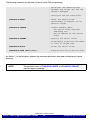
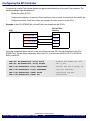
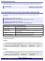
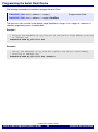
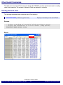
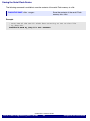
Serial FLASH Programming User’s Guide TRACE32 Online Help TRACE32 Directory TRACE32 Index TRACE32 Documents ...................................................................................................................... FLASH Programming .................................................................................................................... Serial FLASH Programming User's Guide ............................................................................... 1 Introduction ............................................................................................................................. 3 How This Manual is Organized 3 Related Documents 3 Contacting Support 4 List of Abbreviations ............................................................................................................... 6 Background Knowledge ......................................................................................................... 7 What is a Serial Flash Device? 7 About SPI Interface Controllers in Serial Flash Memories 7 About Blocks and Pages 8 File Name Convention for Serial Flash Drivers 9 Standard Approach ................................................................................................................. 10 Identifying and Running Scripts for Serial Flash Programming 10 If There Is No Script 12 Scripts for SPI Controllers ..................................................................................................... 13 Establishing Communication between Debugger and Target CPU 15 Configuring the SPI Controller 16 Resetting Default Values 17 Informing TRACE32 about the Serial Flash Register Addresses (SPI) 17 Informing TRACE32 about the Serial Flash Programming Algorithm 18 Identifying the Correct Driver Binary File for a Serial Flash Device 20 Finding the <serialflash_code> of Your Serial Flash Device 21 Example for SPI Controllers 23 FLASHFILE Declaration Examples 24 Declaration Example for STM32F103 (Cortex-M3) 24 Declaration Example for AT91SAM9XE (ARM9) 25 Checking the Identification from the Serial Flash Device 26 Erasing the Serial Flash Device 27 Programming the Serial Flash Device 28 Copying the Serial Flash Memory 29 Modifying the Serial Flash Memory 31 ©1989-2015 Lauterbach GmbH Serial FLASH Programming User’s Guide 1 Other Useful Commands 32 Reading the Serial Flash 32 Saving the Serial Flash Device 33 Full Examples 34 Example 1 34 Example 2 36 FLASH Programming via Boundary Scan ............................................................................. 37 Example 1 for the SPI Protocol 37 Example 2 for the I2C Protocol 39 ©1989-2015 Lauterbach GmbH Serial FLASH Programming User’s Guide 2 Serial FLASH Programming User’s Guide Version 06-Nov-2015 05-Feb-15 Added section “Finding the <serialflash_code> of Your Serial Flash Device”. Introduction This manual describes the basic concept of serial Flash programming. How This Manual is Organized • Background Information: Provides information about important terms in serial Flash programming, such as SPI interface controller, block, and page. • Standard Approach: Describes the fastest way to get started with SPI serial Flash programming. All you need to do is to identify and run the correct script. Demo scripts for SPI serial Flash programming are provided on the TRACE32 software CD: demo/<architecture>/flash/<*>.cmm e.g. at91sam9xe-spi.cmm, stm32f10x-spi.cmm, str910-spi.cmm, … • New Scripts for SPI Controllers: Describes how you can create a script if there is no demo script for the SPI controller you are using. Related Documents A complete description of all serial Flash programming commands can be found in chapter “FLASHFILE” in ”General Commands Reference Guide F” (general_ref_f.pdf). The manual ”List of Supported FLASH Devices” (flashlist.pdf) provides the following information: • A list of the supported serial Flash memory devices. • A list of the supported CPU families for the serial Flash protocol. ©1989-2015 Lauterbach GmbH Serial FLASH Programming User’s Guide 3 Introduction The Lauterbach home page provides an up-to-date list of • Supported Flash devices under: http://www.lauterbach.com/ylist.html • Supported serial Flash controllers under: http://www.lauterbach.com/ylistnand.html Contacting Support LAUTERBACH GmbH Altlaufstrasse 40 85635 Hoehenkirchen-Siegertsbrunn Germany Phone (+49) 8102-9876-555 Fax (+49) 8102-9876-187 Internet http://www.lauterbach.com/tsupport.html or http://www.lauterbach.com/report.html Here you’ll find local and special support addresses. E-mail [email protected] General support address where your request will be answered within a short time if it is a basic support request or redirected to the appropriate address. Be sure to include detailed system information about your TRACE32 configuration. 1. To generate a system information report, choose TRACE32 > Help > Support > Systeminfo. ©1989-2015 Lauterbach GmbH Serial FLASH Programming User’s Guide 4 Introduction NOTE: Please help to speed up processing of your support request. By filling out the system information form completely and with correct data, you minimize the number of additional questions and clarification request e-mails we need to resolve your problem. 2. Preferred: click Save to File, and send the system information as an attachment to your e-mail. 3. Click Save to Clipboard, and then paste the system information into your e-mail. NOTE: In case of missing script files (*.cmm), please proceed as requested in “If There is No Script” on page 12. ©1989-2015 Lauterbach GmbH Serial FLASH Programming User’s Guide 5 Introduction List of Abbreviations The abbreviations vary from chip manufacturer to chip manufacturer. MOSI or SI Master output, slave input MISO or SO Master input, slave output SCLK or SCK Serial clock SS Slave select SDI Serial data input SDO Serial data output CS or CE CS = Chip selection CE = Chip enable SPI Serial peripheral interface eMMC Embedded multimedia card MMC Multimedia card GPIO General purpose input/output SSI Synchronous serial interface ©1989-2015 Lauterbach GmbH Serial FLASH Programming User’s Guide 6 List of Abbreviations Background Knowledge This chapter of the manual is aimed at users who are new to serial Flash programming; it does not address experts with many years of expertise in this area. This chapter gives you a brief overview of important terms in serial Flash programming, such as serial flash device, sector, page, and SPI interface controller. What is a Serial Flash Device? A serial Flash device is a non-volatile memory that can be electrically erased and reprogrammed. It is used for storing executable code in devices such as DVD players, DSL modems, routers, hard-disk drives, and printers. After power-up, the executable code is downloaded from the serial Flash to RAM, and then executed by the processor. The code in the serial Flash is not changed by the download process and is write-protected. Reasons for the widespread use of serial Flash devices include: • Cost effective and space-saving solution thanks to a reduced number of pins • Low power consumption • Life cycle of about 20 years About SPI Interface Controllers in Serial Flash Memories Serial Flash memories consist of an interface controller (for example, a SPI interface controller) and a Flash memory. Access to the Flash memory is performed by the interface controller on the SPI slave side. SPI Master Controller SPI Slave Processor/ Chip GPIO Core SPI Interface Controller Serial Flash Memory SS SS MOSI MISO SCLK SDI SDO SCLK SPI Interface Controller Flash Memory Figure: Processor/Chip and Serial Flash Memory with a SPI Interface ©1989-2015 Lauterbach GmbH Serial FLASH Programming User’s Guide 7 Background Knowledge Serial Flash memories are controlled by many kinds of serial interface protocols (SPI, SSP, SSI, SMI, etc.). The protocol of the SPI interface (serial peripheral interface) specifies four signals: • Slave select (SS) • Master output, slave input (MOSI) • Master input, slave output (MISO) • Serial clock (SCLK) Most chip manufacturers have proprietary SPI interface controllers (short: SPI controllers) and thus require special driver binary files for programming serial Flash memories. These driver binary files are programs executed by a core in the target and interact with the master SPI controller for controlling the SPI slave controller in order to program the serial Flash memory. Once the required driver binary file was loaded to the target, the TRACE32’s command group FLASHFILE can be used to program and erase the serial Flash memory. Lauterbach provides driver binary files for a large number of SPI controllers. See further down for instructions how to identify the correct driver for your application. About Blocks and Pages The Flash memory of a serial Flash device consists of sectors, and each sector is subdivided into pages; see example diagram below. Page 1 Sector 0 ... ... Page n Flash Memory Sector n Sector A sector is the minimum size unit for erasing. A sector can have a size of 32, 64, or 256 KBytes. The sector sizes are part of the file names of the algorithms required for serial Flash programming: spi32*.bin, spi64*.bin, spi256*.bin. For more information, see “File Name Convention for Serial Flash Drivers” on page 9. Page A page is the minimum size unit for writing and has a size of 256 bytes. ©1989-2015 Lauterbach GmbH Serial FLASH Programming User’s Guide 8 Background Knowledge File Name Convention for Serial Flash Drivers The serial Flash drivers for SPI controllers, i.e. the algorithm files, use the following file name convention: Serial Flash driver name: SPInn_CPU.bin where nn is a two-digit number that indicates the size of one sector in KByte (the sector erase size in KByte): nn Sector Hex Size 32 64 32KB 64KB 0x0--0x7FFF 0x0--0xFFFF where CPU is the CPU family name. ©1989-2015 Lauterbach GmbH Serial FLASH Programming User’s Guide 9 Background Knowledge Standard Approach The chapter “Standard Approach” provides a compact description of the steps required to program serial Flash memories. This description is intentionally limited to the standard use case. Overview of the Standard Approach: • Identify and run the required script for serial Flash programming. • What to do if there is no script for NAND Flash programming. The following step-by-step procedures describe the standard approach in detail. For a detailed description of the serial Flash programming concepts, see “Scripts for SPI Controllers” on page 13. Identifying and Running Scripts for Serial Flash Programming Lauterbach provides scripts (*.cmm) for serial Flash programming which can be found below the TRACE32 installation directory. The scripts support serial Flash memories that have a serial Flash controller with a SPI interface (short: SPI controller). Path and file name convention of scripts to be used with SPI controllers: <TRACE32_installation_directory>/ demo/<architecture>/flash/<cpu_name>-spi.cmm To identify and run the required script: 1. Make a note of the <cpu_name> printed on the CPU; for example, bcm5357 2. Put the <cpu_name> and spi together to form the script name: bcm5357-spi.cmm tbd. The script file resides in this folder: ~~/demo/mips/flash/bcm5357-spi.cmm Note: ~~ is replaced by the <TRACE32_installation_directory>, which is c:/T32 by default.) If the folder does not contain the script you are looking for, see “If There Is No Script” on page 12. 3. Run the script in TRACE32 by doing one of the following: - Choose File > Run Batch File <script name> ©1989-2015 Lauterbach GmbH Serial FLASH Programming User’s Guide 10 Standard Approach - In the command line, type DO <path and script name> NOTE: Each script (*.cmm) includes a reference to the required serial Flash programming algorithm (*.bin). You do not need to program or select the algorithm. Example ; <code_range> <data_range> <algorithm_file> FLASHFILE.TARGET 0x80020000++0x1FFF 0x80022000++0x3FFF ~~/demo/mips/flash/byte_le/spi64_bcm5357.bin ©1989-2015 Lauterbach GmbH Serial FLASH Programming User’s Guide 11 Standard Approach If There Is No Script If there is no script for your device in this directory (<TRACE32_installation_directory>/demo/ <architecture>/flash/), then please send a request to [email protected] using the e-mail template below. E-Mail Template: Chip name: ______________________ Name of serial Flash device: ________ Provide the CPU datasheet for us: ___________ Lend the target board to us by sending it to the address given in “Contacting Support”: ________ <SystemInformation> Be sure to include detailed system information about your TRACE32 configuration. For information about how to create a system information report, see “Contacting Support”. Normally we can provide support for a new device in two weeks. If our support cannot provide you with a script, you will have to create your own script (*.cmm). For more information about how to create your own script (*.cmm), see “Scripts for SPI Controllers” on page 13. ©1989-2015 Lauterbach GmbH Serial FLASH Programming User’s Guide 12 Standard Approach Scripts for SPI Controllers This chapter describes how to create new scripts for serial Flash memories that are equipped with SPI controllers. The steps and the framework (see below) provide an overview of the process. They are described in detail in the following sections. The following steps are necessary to create a new script: 1. “Establishing Communication between Debugger and Target CPU”, page 15 2. “Configuring the SPI Controller”, page 16 3. “Resetting Default Values”, page 17 4. “Informing TRACE32 about the Serial Flash Register Addresses (SPI)”, page 17 5. “Informing TRACE32 about the Serial Flash Programming Algorithm”, page 18 6. “Checking the Identification from the Serial Flash Device”, page 26 7. “Erasing the Serial Flash Device”, page 27 8. “Programming the Serial Flash Device”, page 28 ©1989-2015 Lauterbach GmbH Serial FLASH Programming User’s Guide 13 Scripts for SPI Controllers The following framework can be used as base for serial Flash programming: ; Establish the communication ; between the target CPU and the ; TRACE32 debugger. ; Configure the SPI controller. FLASHFILE.RESet ; Reset the serial Flash ; environment in TRACE32 to its ; default values. FLASHFILE.CONFIG … ; Inform TRACE32 about ; - the serial Flash register ; addresses and ; - the CS address of the serial ; Flash FLASHFILE.TARGET … ; Specify the serial Flash ; programming algorithm and where ; it runs in target RAM. FLASHFILE.Erase … ; Erase the serial Flash. FLASHFILE.LOAD <main_file> … ; Program the file to serial Flash. An ellipsis (…) in the framework indicates that command parameters have been omitted here for space economy. NOTE: The parametrization of FLASHFILE.CONFIG and FLASHFILE.TARGET requires expert knowledge. ©1989-2015 Lauterbach GmbH Serial FLASH Programming User’s Guide 14 Scripts for SPI Controllers Establishing Communication between Debugger and Target CPU Serial Flash programming with TRACE32 requires that the communication between the debugger and the target CPU is established. The following commands are available to set up this communication: SYStem.CPU <cpu> Specify your target CPU. SYStem.Up Establish the communication between the debugger and the target CPU. SYStem.CPU STM32F103 ; Select STM32F103 as the target CPU. SYStem.Up ; Establish the communication between the ; debugger and the target CPU. ©1989-2015 Lauterbach GmbH Serial FLASH Programming User’s Guide 15 Scripts for SPI Controllers Configuring the SPI Controller Programming a serial Flash device requires an appropriate initialization of the serial Flash interface. The following settings might be necessary: • Enable the clock (SCLK). • Configure the registers of the serial Flash interface, such as clock, master/slave, data width, etc. • Configure the serial Flash pins if they are muxed with other functions of the CPU. Example: In the CPU STM32F103, all the SPI pins are muxed with the GPIOs. Serial Flash Memory CPU STM32F103 GPIO.A4 / SS SS GPIO.A5 / SCLK SCLK GPIO.A6 / MISO SDI GPIO.A7 / MOSI SDO Using the commands below, the pins of the serial Flash interface (SPI) can be configured for the CPU STM32F103. The resulting configuration allows the CPU to switch from the GPIO A4-A7 to SS,SCLK, MISO, and MOSI. PER.Set SD:0x40021014 %Long 0x114 PER.Set SD:0x40021018 %Long 0x100C ; Enable the Clock for the ; SPI & PIO. PER.S SD:0x40010800 %Long 0xbbb34444 PER.S SD:0x40010810 %Long 0xFFFFFFF ; Switch the PIO.A group to ; the SPI function. PER.S SD:0x40013000 %WORD 0x34F PER.S SD:0x40013010 %WORD 0x7 ; Configure the SPI ; controller. ©1989-2015 Lauterbach GmbH Serial FLASH Programming User’s Guide 16 Scripts for SPI Controllers Resetting Default Values The following command is used to reset the serial Flash environment in TRACE32 to its default values. FLASHFILE.RESet Reset the serial Flash environment in TRACE32 to its default values. Informing TRACE32 about the Serial Flash Register Addresses (SPI) The following command is used to inform TRACE32 about the various register addresses (Flash declaration). Chip selection is controlled by one GPIO pin. FLASHFILE.CONFIG <SPI Tx reg> <SPI Rx reg> <CS GPIO reg> <CS bit> Chip selection is controlled by the SPI controller. FLASHFILE.CONFIG <SPI Tx reg> <SPI Rx reg> <SPI ChipEnable reg> Parameters for the FLASHFILE.CONFIG command <SPI Tx reg> The transmit data register <SPI Rx reg> The receive data register <CS GPIO reg> The chip selection GPIO register which is connected to the Flash chip selection <CS bit> The chip selection bit in the GPIO CS register <SPI ChipEnable reg> The chip enable register of the serial flash For information about the register addresses and the CS bit, refer to the manufacturer’s microcontroller manual and the schematics. Example 1 ; For the serial Flash CS connected PIO A.4 (group A, port number 4) ; PIO group A register 0x4001080C ; <SPI Tx reg> <SPI Rx reg> <CS GPIO reg> <CS bit> FLASHFILE.CONFIG 0x4001300C 0x4001300C 0x4001080C 0x4 Example 2 ; The AT91SAM9XE’s CS is controlled by the SPI register 0xFFFC8000, not ; the specified GPIO ports. ; <SPI Tx reg> <SPI Rx reg> <SPI ChipEnable reg> FLASHFILE.CONFIG 0xFFFC800C 0xFFFC8008 0xFFFC8000 ©1989-2015 Lauterbach GmbH Serial FLASH Programming User’s Guide 17 Scripts for SPI Controllers Informing TRACE32 about the Serial Flash Programming Algorithm The following command is available to inform TRACE32 about the serial Flash programming algorithm: FLASHFILE.TARGET <code_range> <data_range> <file> Specify the serial Flash programming driver and where it runs in the target RAM. Parameters • <code_range> Define an address range in the target´s RAM to which the serial Flash programming algorithm is loaded. FLASH algorithm 32 byte Figure: Memory mapping for the <code_range> Required size for the code is size_of(<file>) + 32 byte • <data_range> Define the address range in the target´s RAM where the programming data is buffered for the programming algorithm. ©1989-2015 Lauterbach GmbH Serial FLASH Programming User’s Guide 18 Scripts for SPI Controllers 64 byte argument buffer buffer for programming data 256 byte stack Figure: Memory mapping for the <data_range> The argument buffer used for the communication between the TRACE32 software and the programming algorithm is located at the first 64 bytes of <data_range>. The 256 byte stack is located at the end of <data_range>. <buffer_size> = size_of(<data_range>) - 64 byte argument buffer - 256 byte stack <buffer_size> is the maximum number of bytes that are transferred from the TRACE32 software to the serial Flash programming algorithm in one call. • <file> Lauterbach provides ready-to-run driver binary files for serial Flash programming. They are located in the TRACE32 installation directory: ~~/demo/<architecture>/flash/byte/ Note: ~~ is expanded to the <TRACE32_installation_directory>, which is c:/T32 by default. For detailed information about how to determine the <file> parameter, see “Identifying the Correct Driver Binary File for a Serial Flash Device” on page 20. ©1989-2015 Lauterbach GmbH Serial FLASH Programming User’s Guide 19 Scripts for SPI Controllers Identifying the Correct Driver Binary File for a Serial Flash Device There are two ways to find the correct *.bin file: • You can identify the *.bin file via our website, as described in this section. • Alternatively, run a PRACTICE script (*.cmm), as described in “Finding the <serialflash_code> of Your Serial Flash Device”, page 21. To identify the correct *.bin file: 1. For information about supported Flash devices, access the Lauterbach website. 2. Click the + drill-down button next to Tool Chain, and then click Supported NAND/Serial Flash Controller (http://www.lauterbach.com/ylistnand.html). 3. Open Supported Flash Devices in a separate window or tab (http://www.lauterbach.com/ylist.html). 4. On the Supported Flash Devices page, select the required company from the drop-down list. 5. Locate the desired Flash device. You need the name of the Flash device to be able to identify the correct driver binary file. 6. Identify the correct *.bin file based on the name of the Flash device. The following example illustrate how to do this. - The example below illustrates how to apply the file name convention in practice. - For information about the file name convention for driver binary files, see “File Name Convention for Serial Flash Drivers” on page 9. tbd. ©1989-2015 Lauterbach GmbH Serial FLASH Programming User’s Guide 20 Scripts for SPI Controllers Finding the <serialflash_code> of Your Serial Flash Device The following step-by-step procedure helps you find the <serialflash_code> of your serial Flash device. Based on the <serialflash_code>, you can then identify the correct *.bin file. To find the <serialflash_code>: 1. Run the following PRACTICE script file (*.cmm) from the TRACE32 demo folder: CD.DO ~~\demo\etc\flash\find_spidef.cmm ;The path prefix ~~ expands to the system directory of TRACE32, ;by default C:\t32. If this demo script is missing, you can download it from www.lauterbach.com/scripts.html. The Find SPI flash code dialog opens. 2. Under spi flash parameters, make your settings. - You can find the required information in the serial Flash documentation of the manufacturer. - For an example of where to search for the information, see figure and table below: A In the serial Flash documentation of the manufacturer, search for terms like: - erase capability - sector - granularity in order to find the correct value. B C Instruction Description One-Byte Instruction Code (BIN) One-Byte Address Dummy Instruction Bytes Clock Code (HEX) Cycle Data Bytes ... A READ Read Data Bytes 0000 0011 03h 3/4 0 1 to Page Program 0000 0010 02h 3/4 0 1 to 256 Read Flag Status Register 0111 0000 70h 0 0 1 to ... B PP ... C RFSR ©1989-2015 Lauterbach GmbH Serial FLASH Programming User’s Guide 21 Scripts for SPI Controllers 3. Click Find. - The code box displays the <serialflash_code> of your serial Flash device. - If the code box displays unknown, then proceed as described in “If There is No Script”. 4. Make a note of the displayed <serialflash_code>. 5. Click End to close the dialog. 6. Identify the correct *.bin file based on the <serialflash_code>. The following example illustrates how to do this. - “Example for SPI Controllers”, page 23 - For information about the file name convention for driver binary files, see “File Name Convention for Serial Flash Drivers” on page 9. ©1989-2015 Lauterbach GmbH Serial FLASH Programming User’s Guide 22 Scripts for SPI Controllers Example for SPI Controllers Target: • ARM-based STM32F10X CPU with the SPI controller stm • Serial Flash device M25P64 Taken together, the Code column and the Controller column make up the file name of the serial Flash driver binary file: spi64_stm.bin. The number 64 indicates the size of one sector in KByte (the sector erase size in KByte). The binary file resides in this folder: ~~/demo/arm/flash/byte Note: ~~ is expanded to the <TRACE32_installation_directory>, which is c:/T32 by default. This results in the following command line: ; Specify the serial Flash programming algorithm and where it runs in ; the target RAM. <code_range> <data_range> <file> FLASHFILE.TARGET 0x20000000++0x1FFF 0x20002000++0x1FFF ~~/demo/arm/flash/byte/spi64_stm.bin ©1989-2015 Lauterbach GmbH Serial FLASH Programming User’s Guide 23 Scripts for SPI Controllers FLASHFILE Declaration Examples Declaration Example for STM32F103 (Cortex-M3) STM32F103 (ARM Cortex-M3) from ST Microelectronics, M25P64 (64Mbit) • SPI Tx register/SPI Rx register: 0x4001300C • Sector size: 64Kbytes (0x0--0xFFFF) • Driver file: ~~/demo/arm/flash/byte_thumb/spi64_stm.bin Note: ~~ is expanded to the <TRACE32_installation_directory>, which is c:/T32 by default. … ; Reset the FLASHFILE declaration within TRACE32. FLASHFILE.RESet ; For the serial Flash CS connected PIO A.4 (Group A, port Number4) ; PIO group A register 0x4001080C ; <SPI Tx reg> <SPI Rx reg> <CS GPIO reg> <CS bit> FLASHFILE.CONFIG 0x4001300C 0x4001300C 0x4001080C 0x4 ; Specify the serial Flash programming algorithm and where it runs on ; the target RAM. FLASHFILE.TARGET 0x20000000++0x1FFF 0x20002000++0x1FFF ~~/demo/arm/flash/byte_thumb/spi64_stm.bin … ©1989-2015 Lauterbach GmbH Serial FLASH Programming User’s Guide 24 Scripts for SPI Controllers Declaration Example for AT91SAM9XE (ARM9) AT91SAM9XE (ARM9) from ATMEL, M25P64 (64Mbit) • SPI Tx register/SPI Rx register: 0xFFFC800C / 0xFFFC8008 • Sector size: 64Kbytes (0x0--0xFFFF) • Driver file: ~~/demo/arm/flash/byte/spi64_at91sam9xe.bin Note: ~~ is expanded to the <TRACE32_installation_directory>, which is c:/T32 by default. . … ; Reset the FLASHFILE declaration within TRACE32. FLASHFILE.RESet ; The AT91SAM9XE’s CS is controlled by the SPI register 0xFFFC8000 not ; the specified GPIO ports. ; <SPI Tx reg> <SPI Rx reg> <SPI ChipEnable reg> FLASHFILE.CONFIG 0xFFFC800C 0xFFFC8008 0xFFFC8000 ; Specify the serial Flash programming algorithm and where it runs on ; the target RAM. FLASHFILE.TARGET 0x300000++0x1FFF 0x302000++0x1FFF ~~/demo/arm/flash/byte/spi64_at91sam9xe.bin … ©1989-2015 Lauterbach GmbH Serial FLASH Programming User’s Guide 25 Scripts for SPI Controllers Checking the Identification from the Serial Flash Device The following command can be used to check if TRACE32 can access the serial Flash device: FLASHFILE.GETID Get the ID values of the serial Flash device. ; Open the TRACE32 AREA window. AREA.view ; Check the access to the serial Flash device ; by getting the manufacturer ID and the device ID. FLASHFILE.GETID ©1989-2015 Lauterbach GmbH Serial FLASH Programming User’s Guide 26 Scripts for SPI Controllers Erasing the Serial Flash Device The following command is available to erase serial Flash devices: FLASHFILE.Erase <range> NOTE: Erase the serial Flash. The FLASHFILE.Erase command has a time limitation. • TRACE32 has to get a response (success or failure) from the serial Flash in 3 minutes. • If you get an error message because of the FLASHFILE.Erase time limitation, then divide the original range into several smaller ranges. Example 1: Original erase range ; Erase 2MB starting from 0x0. FLASHFILE.Erase 0x0--0x1FFFFF Example 1 cont’d: Two smaller erase ranges ; Erase 2MB starting from 0x0. FLASHFILE.Erase 0x0--0xFFFFF FLASHFILE.Erase 0x100000--0x1FFFFF Example 2: Erase 8 MB in increments of 1 MB using a RePeaT loop &addr=0x0 RePeaT 8. ( FLASHFILE.Erase &addr++0xFFFFF &addr=&addr+0x100000 ) ©1989-2015 Lauterbach GmbH Serial FLASH Programming User’s Guide 27 Scripts for SPI Controllers Programming the Serial Flash Device The following commands are available to program the serial Flash: FLASHFILE.LOAD <file> [<address> | <range>] Program serial Flash. FLASHFILE.LOAD <file> [<address> | <range>] /ComPare The data from <file> is written to the address range specified by <range>. If no <range> or <address> is specified, programming starts at address 0x0. Example 1 ; Program the contents of my_file.bin to the serial Flash memory starting ; at address 0x0. FLASHFILE.LOAD my_file.bin 0x0 Example 2 ; Verify the contents of my_file.bin against the serial Flash memory ; starting at address 0x0. FLASHFILE.LOAD my_file.bin 0x0 /ComPare ©1989-2015 Lauterbach GmbH Serial FLASH Programming User’s Guide 28 Scripts for SPI Controllers Copying the Serial Flash Memory The following command is available to copy: • Any data from any CPU memory area to the serial Flash memory, or • Any data from one address range of the serial Flash to another address range within the same serial Flash memory; for example, for backup purposes. FLASHFILE.COPY <source range> <target addr> Copy data from the source range to the defined address of the serial Flash. FLASHFILE.COPY <source range> <target addr> /ComPare Verify the source range data against the target range data. Example 1 ; Copy the 1MB virtual memory data at 0x0 to the serial Flash address ; at 0x100000. ; VM: The virtual memory of the TRACE32 software. FLASHFILE.COPY VM:0x0--0xFFFFF 0x100000 Result (1) Data is copied from the CPU to the serial Flash Example 2 ; Verify the data between virtual memory and serial Flash. FLASHFILE.COPY VM:0x0--0xFFFFF 0x100000 /ComPare ©1989-2015 Lauterbach GmbH Serial FLASH Programming User’s Guide 29 Scripts for SPI Controllers Example 3 ; Copy the 1MB serial Flash data at 0x0 to the serial Flash ; at 0x800000. FLASHFILE.COPY 0x0--0xFFFFF 0x800000 ; Verify the 1MB serial Flash data between 0x0 and 0x800000. FLASHFILE.COPY 0x0--0xFFFFF 0x800000 /ComPare ©1989-2015 Lauterbach GmbH Serial FLASH Programming User’s Guide 30 Scripts for SPI Controllers Modifying the Serial Flash Memory The following command is available to modify the contents of the serial Flash memory. The maximum range that one FLASHFILE.Set command can modify is only one sector of the Flash memory. If you want to modify three sectors, you need three FLASHFILE.Set commands, etc. FLASHFILE.Set [<address> | <range>] %<format> <data> Modify the contents of the serial Flash. Example 1 ; Write 4 bytes of data 0x12345678 to the address 0x100000. ; LE = little endian FLASHFILE.Set 0x100000 %LE %Long 0x12345678 Example 2 ; Write data 0x0 to the address range 0x100000++0xFFF. FLASHFILE.Set 0x100000++0xFFF %Byte 0x0 Result (1) Result (2) Example 3 ; A serial Flash has 64KB per sector (0x10000). ; Write data 0x0 from 0x100000 to 0x12FFFF in the serial Flash. FLASHFILE.Set 0x100000++0xFFFF %Long 0x0 FLASHFILE.Set 0x110000++0xFFFF %Long 0x0 FLASHFILE.Set 0x120000++0xFFFF %Long 0x0 ©1989-2015 Lauterbach GmbH Serial FLASH Programming User’s Guide 31 Scripts for SPI Controllers Other Useful Commands The CPU cannot read serial Flash memories directly. But TRACE32 provides special commands for reading serial Flash memories. The contents of the serial Flash are displayed in a window. Reading the Serial Flash The following command allows to read the serial Flash memory. FLASHFILE.DUMP [<address>] [/<format>] Display a hex-dump of the serial Flash. Example ; Display a hex-dump of the serial Flash starting at 0x1000. ; Display the information in a 32-bit format (/Long option). FLASHFILE.DUMP 0x1000 /Long Result ©1989-2015 Lauterbach GmbH Serial FLASH Programming User’s Guide 32 Scripts for SPI Controllers Saving the Serial Flash Device The following command is available to save the contents of the serial Flash memory to a file. FLASHFILE.SAVE <file> <range> Save the contents of the serial Flash memory into <file>. Example ; Save 1MB of the serial Flash data starting at 0x0 to the file ; my_dump.bin. FLASHFILE.SAVE my_dump.bin 0x0--0xFFFFF ©1989-2015 Lauterbach GmbH Serial FLASH Programming User’s Guide 33 Scripts for SPI Controllers Full Examples Example 1 CPU: STM32F103 (Cortex-M3 core) Serial Flash: M25P64 (STMicroelectronics, 64Mbit) Serial Flash CS: Connected to GPIO B.2 RESet SYStem.RESet SYStem.CPU STM32F103ZE SYStem.Up gosub enable_SPI ; Reset the Flash declaration within TRACE32. FLASHFILE.RESet ; For the serial Flash CS connected GPIO B.2 (group B, port number2) ; GPIO B.2 data output register 0x40010C0C ; <SPI Tx reg> <SPI Rx reg> <CS GPIO reg> <CS bit> FLASHFILE.CONFIG 0x4001300C 0x4001300C 0x40010C0C 0x2 FLASHFILE.TARGET 0x20000000++0x1fff 0x20002000++0x1FFF ~~/demo/arm/flash/byte_thumb/spi64_stm.bin ; Read Flash manufacture and device ID. FLASHFILE.GETID ; Erase serial Flash. FLASHFILE.Erase 0x0--0xFFFFF ; Program my_file.bin to serial Flash. FLASHFILE.LOAD my_file.bin 0x0 ©1989-2015 Lauterbach GmbH Serial FLASH Programming User’s Guide 34 Scripts for SPI Controllers ; Save to my_dump.bin from serial Flash FLASHFILE.SAVE my_dump.bin 0x0--0xFFFFF enable_SPI: ; Clock Enable related with the SPI and GPIO group PER.S SD:0x40021014 %Long 0x114 ; FSCM Clock Enable PER.S SD:0x40021018 %Long 0x100C ; SPI1 & GPIO A/B Enable PER.S SD:0x40010C00 %LONG 44444344 ; GPIOB.2 output PER.S SD:0x40010C0C %LONG 00000004 ; deselect the SPI FLASH CS(GPIOB.2) PER.S SD:0x40013000 %WORD 0x30F ; SPI_Init PER.S SD:0x40013010 %WORD 0x7 ; SPI_CRC pol &spi_enable=Data.word(SD:0x40013000)|0x40 PER.S SD:0x40013000 %WORD &spi_enable ; SPI1 Enable return ENDDO ©1989-2015 Lauterbach GmbH Serial FLASH Programming User’s Guide 35 Scripts for SPI Controllers Example 2 CPU: The STR91x is based on a ARM966E core. It has a SSP protocol which is similar to a STM SPI controller. Serial Flash: ST Microelectronics M25P64 (64Mbit) Serial Flash is connected to GPIO 5.7 on the STR91x. Then it is controlled by GPIO5 register (0x5800B3FC). ; Select str910 as target CPU. ; Establish the communication between the debugger and the target CPU. SYStem.RESet SYStem.CPU STR910 SYStem.Option ResBreak OFF SYStem.JtagClock RTCK SYStem.Up ; Enable SSP (Synchronous Serial Peripheral) & configuration of pins. PER.Set ASD:0x5C002018 %Long 0x80300 PER.Set ASD:0x5C002020 %Long 0x80300 PER.Set ASD:0x5C002028 %Long 0x80300 PER.Set ASD:0x5800B400 %Long 0xb0 PER.Set ASD:0x5C002058 %Long 0x4a00 PER.Set ASD:0x5C002098 %Long 0x0 PER.Set ASD:0x5C002078 %Long 0x40 PER.Set ASD:0x5C007000 %Long 0x5c7 ;SSP0_CR0 PER.Set ASD:0x5C007010 %Long 0x2 ;SSP0_PR PER.Set ASD:0x5C007004 %Long 0x2 ;SSP0 Enable FLASHFILE.RESet ; <SPI Tx Reg> FLASHFILE.CONFIG 0x5C007008 <SPI Rx Reg> <CS GPIO reg> <CS bit> 0x5C007008 0x5800B3FC 0x7 ; <code_range> <data_range> <algorithm_file> FLASHFILE.TARGET 0x4000000++0x1FFF 0x4002000++0x1FFF ~~/demo/arm/flash/byte/spi64_stm.bin ; Programming for the serial Flash FLASHFILE.GETID FLASHFILE.ERASE 0x0--0xFFFFF FLASHFILE.LOAD * 0x0 FLASHFILE.SAVE dump.bin 0x0--0xFFFFF ENDDO ©1989-2015 Lauterbach GmbH Serial FLASH Programming User’s Guide 36 Scripts for SPI Controllers FLASH Programming via Boundary Scan The BSDL commands of TRACE32 are used to program external FLASH memories via boundary scan. Important BSDL-specific steps are: • Check that the bypass mode works. • Check that the IDCODE matches. • Define the FLASH pin connection. • Enable serial FLASH programming via boundary scan and define the flash type. Serial FLASH programming then continues with the FLASHFILE commands described in this manual. The following PRACTICE script (*.cmm) illustrates the BSDL-specific steps by way of these examples: • Example 1 for the SPI protocol • Example 2 for the I2C protocol Example 1 for the SPI Protocol CPU: AT91SAM3U4 Serial FLASH: M25P64 (STMicroelectronics, 64Mbit) Pin connection: SPI_CE: Port A16 SPI_SCK: Port A15 SPI_MOSI: Port A14 SPI_MISO: Port A13 ©1989-2015 Lauterbach GmbH Serial FLASH Programming User’s Guide 37 FLASH Programming via Boundary Scan SYStem.JtagClock 15.Mhz BSDL.RESet BSDL.FILE ./sam3u4e_lqfp144.bsd ; set JTAG clock ; reset boundary scan configuration ; load the required BSDL file BSDL.HARDRESET BSDL.SOFTRESET ; toggle TRST_N pin ; do a sequential JTAG reset IF BSDL.CHECK.BYPASS() ( IF BSDL.CHECK.IDCODE() ( BSDL.FLASH.IFDefine RESet ; check, if BYPASS mode works ; check, if the IDCODE matches ; ; BSDL.FLASH.IFDefine SPI 1. ; ; ; ; reset the boundary scan flash configuration define boundary scan flash interface: - protocol: SPI - SPI flash memory connected to IC1 of the boundary scan chain BSDL.FLASH.IFMap CE BSDL.FLASH.IFMap SCK BSDL.FLASH.IFMap SI BSDL.FLASH.IFMap SO BSDL.FLASH.INIT SAFE PA16 PA15 PA14 PA13 map generic SPI pin CE to port PA16 map generic SPI pin SCK to port PA15 map generic SPI pin SI to port PA14 map generic SPI pin SO to port PA13 Initialize boundary scan chain to safe values according to SAFE state from BSDL file FLASHFILE.BSDLaccess ON ; ; ; ; ; ; ; ; Enable serial flash programming via ; boundary scan FLASHFILE.BSDLFLASHTYPE SPI64 ; define serial flash type FLASHFILE.GETID ; get the SPI flash memory ID ; continue with serial flash programming, e.g.: ; FLASHFILE.DUMP 0x0 ; FLASHFILE.ERASE 0x0--0xFFFFF ; FLASHFILE.LOAD * 0x0 ) ) ENDDO ©1989-2015 Lauterbach GmbH Serial FLASH Programming User’s Guide 38 FLASH Programming via Boundary Scan Example 2 for the I2C Protocol CPU: AT91SAM3U4 eMMC FLASH: ST24C08 (STMicroelectronics, 8kbit) Pin connection: I2C_SCL: Port A25 I2C_SDA: Port A24 SYStem.JtagClock 15.Mhz ; set JTAG clock BSDL.RESet ; reset boundary scan configuration BSDL.FILE ./sam3u4e_lqfp144.bsd ; load the required BSDL file BSDL.HARDRESET BSDL.SOFTRESET ; toggle TRST_N pin ; do a sequential JTAG reset IF BSDL.CHECK.BYPASS() ( IF BSDL.CHECK.IDCODE() ( BSDL.FLASH.IFDefine RESet ; check, if BYPASS mode works ; check, if the IDCODE matches ; reset the boundary scan flash ; configuration BSDL.FLASH.IFDefine I2C 1. ; define boundary scan flash interface: ; - protocol: I2C ; - I2C flash memory connected to IC1 of ; the boundary scan chain BSDL.FLASH.IFMap SCL BSDL.FLASH.IFMap SDA BSDL.FLASH.INIT SAFE PA25 ; map generic I2C pin PA24 ; map generic I2C pin ; Initialize boundary ; values according to ; from BSDL file SCL to port PA25 SDA to port PA24 scan chain to safe SAFE state FLASHFILE.BSDLaccess ON ; Enable serial flash programming via ; boundary scan FLASHFILE.BSDLFLASHTYPE I2C08 ; define serial flash type FLASHFILE.GETID ; get the I2c flash memory ID ; continue with serial flash programming, e.g.: ; FLASHFILE.DUMP 0x0 ; FLASHFILE.ERASE 0x0--0x3FF ; FLASHFILE.LOAD * 0x0 ) ) ENDDO ©1989-2015 Lauterbach GmbH Serial FLASH Programming User’s Guide 39 FLASH Programming via Boundary Scan