1
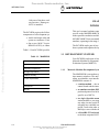
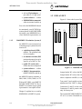
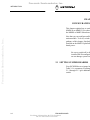
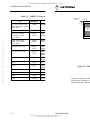
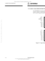
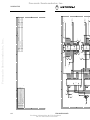
Freescale Semiconductor, Inc. CONTENTS INDEX ..................................................................................................................................index-1 Freescale Semiconductor, Inc... FIGURES 1-1 3-1 3-2 3-3 M68EML908RC24 Emulator Module ............................................................................. 1-3 TARGET Connectors J1, J2 Pin Assignments.................................................................. 3-1 Logic Analyzer Connectors J3, J4 Pin Assignments......................................................... 3-3 Target Cable Assembly ..................................................................................................... 3-5 M68EML9 TABLES 1-1 2-1 3-1 3-2 3-3 EMULATOR M68EML908RC24 Specifications.................................................................................... 1-4 Jumper Headers................................................................................................................. 2-2 TARGET Connector J1, J2 Signal Descriptions............................................................... 3-2 Logic Analyzer Connector J3 Signal Descriptions ........................................................... 3-4 Logic Analyzer Connector J4 Signal Descriptions ........................................................... 3-4 USER’S M © MOTOROLA Inc., 199 For More Information On This Product, Go to: www.freescale.com Freescale Semiconductor, Inc. CONT Freescale Semiconductor, Inc... CHAPTER 1 I Motorola reserves the right to make changes without further notice to any products herein to improve reliability, function, or Motorola does not 1.1design. Development Systems................................ assume any liability arising out of the application or 1.1.1 use of any product or circuit Motorola Modular Development Syst described herein; neither does it convey any license under its patent rights nor the 1.2 EM Layout.................................................. rights of others. Motorola products are not designed, intended, or authorized for 1.3implant Customer Support....................................... use as components in systems intended for surgical into the body, or other application in which the failure of the Motorola product could create a situation where personal injury or death may occur. Should Buyer purchase or use 2 CHAPTER CONFIGUR Motorola products for any such unintended or unauthorized application, Buyer shall indemnify and hold Motorola and its officers, subsidiaries, 2.1employees, Setting Jumper Headers.............................. affiliates, and distributors harmless against all claims,2.1.1 costs,Setting damages, and the External Clock Source He expenses, and reasonable attorney fees arising out of,2.1.2 directly or indirectly, anycontrol source (W2 Setting the VMCU claim of personal injury or death associated with such unintended or unauthorized 2.1.3 Adjusting VMCU (E1, R26)................. use, even if such claim alleges that Motorola was negligent regarding the design 2.2 Remaining System Installation................... or manufacture of the part. 2.3 Substituting Microcontrollers..................... Motorola and the Motorola logo are registered trademarks of Motorola Inc. CHAPTER 3 Motorola Inc. is an Equal Opportunity/Affirmative Action Employer. 3.1 3.2 3.3 CONNE Target Connectors (J1, J2) ......................... Logic Analyzer Connectors (J3, J4) ........... Target Cable Assemblies............................ CHAPTER 4 SCHEMATICS ..................................................... For More Information On This Product, Go to: www.freescale.com Freescale Semiconductor, Inc. INTRODUCTION CAUTION Only one of the three sockets U1, U2, or U12 can be populated at any one time. Damage to the system will occur if more than one MCU is installed. CHAP INTROD Freescale Semiconductor, Inc... This user’s The RC24EM requires the following user-supplied cables for connection tomanual other explains conne specific to the M68EML908RC24 components of a development system: makes possible emulation and deb • An 80-lead target cable and Target Head Adapter, to connect the target MC68HC908RC24 microcontrolle system to connectors J1 and J2. emulator, operating in the range 1 • One or two 100-KΩ logic analyzer termination adapters (HP part number The RC24EM can be part of two d HP01650-63203), to connect to connectors J3 or J4. those systems and explains the lay Table 1-1 lists RC24EM specifications. 1.1 DEVELOPMENT SYSTEMS Table 1-1. M68EML908RC24 Specifications Your RC24EM can be part of two Motorola Modular Development S Specifications Evaluation System (MMEVS). Characteristic MCU extension I/O ports HCMOS compatible Operating temperature 0° to 40° C Storage temperature -40° to +85° C Relative humidity 0 to 90% (non-condensing) Power requirements 1.1.1 Motorola Modular Development Syste The MMDS0508 is an emulator sy time memory windows. The unit’s anpump), assembler, user interfac 5 volts dc and 12 volts dceditor, (charge provided from the MMDSMMDS0508 control boardconsists or of: MMEVS platform board • a station module — the me board and the intern Dimensions 8.15 x 4.5 inches (207 x 115 mm) control Weight 7.1 ounces (201 g) • an emulator module (EM) purchased printed circuit bo specific set of MCUs. • two logic clip cable assem station module to your targe any other circuitry useful fo assembly has a molded con pod B. Leads at the other en Ball clips come with the cab • a 9-lead RS-232 serial cab to the host computer RS-23 1-4 EML908RC24UM/D EML908RC24UM/D For More Information On This Product, Go to: www.freescale.com Freescale Semiconductor, Inc. INTRODUCTION • a 9- to 25-pin adapter — a molded assembly that lets you connect the 9pin cable to a 25-pin serial port. 1.2 EM LAYOUT • system software — software, on 3-1/2 inch diskettes. Figure 1-1 shows the layout of the • MMDS0508 documentation — an MMDS0508 user's manual, a system software manual, and the appropriate EM user's manual. Freescale Semiconductor, Inc... You select the MMDS0508 baud rate: 2400, 4800, 9600, 19200, 38400, or 57600. U1 As mentioned, your RC24EM gives the MMDS0508 the target J3ability J4 to emulate P1 systems based on MC68HC908RC24 MCUs. By substituting a different EM, you can enable your MMDS0508 to emulate target systems based on a different MCU. (Your Motorola representative can explain all the EMs available.) 1.1.2 M68MMEVS Evaluation System (MMEVS) An MMEVS is an economical, two-board tool for designing, debugging, and evaluating target systems based on an MC68HC0508 MCU. A complete MMEVS consists of: U12 • a platform board (PFB) — the bottom board, which supports the emulator module. The platform board has connectors for power and for the terminal or host computer. W1 • an emulator module (EM) — such as the RC24EM: a separately purchased printed circuit board that enables system functionality for a specific set of MCUs. The EM fits onto the PFB. J5 U13 • an RS-232 serial cable — a separately purchased cable that connects the PFB to the host computer RS-232 port. Figure 1-1. M68EML908 • system software — software, on 3-1/2 inch diskettes. • MMEVS documentation — an MMEVS operations manual Jumper header W1 selects the MC (MMEVSOM/D) and the appropriate EM user's manual. Jumper header W2 selects the refe An MMEVS features automatic selection of the communicationeither baud rate: 2400, with R26, or can is adjusted 4800, 9600, 19200, 38400, or 57600. Test point E1 and variable resistor With an RC24EM, your MMEVS emulates target systems basedadjustment on of the VMCU voltage, MC68HC908RC24 MCUs. By substituting a different EM, you can enable your MMEVS to emulate target systems based on a different MCU. (Your Motorola Connectors J1 and J2 are the custo representative can explain all the EMs available.) Connectors J3 and J4 permit conn only for factory test. Chapter 2 explains how to configure and use your RC24EM as part of an MMDS0508 or MMEVS system. The resident MC68HC908RC24 M U5 or U2, or in the Clamshell soc 1-2 EML908RC24UM/D EML908RC24UM/D For More Information On This Product, Go to: www.freescale.com Freescale Semiconductor, Inc. CONFIGURATION AND OPERATION Table 2-1. Jumper Headers 1.3 CUSTOMER SUPPORT Header Clock Source Select, W1 Position W1 XTAL 1 2 CAN MMDS 6 5 Freescale Semiconductor, Inc... OSC SELECT W1 XTAL 1 2 CAN MMDS 6 5 For information about a Motorola Effect OSC SELECT Selects a user-supplied crystal as the signal source. (Requires user installation AUSTRALIA, Melbourne – (61-3)887-0711 of crystal at Y1, resistors R19 and Sydney – at 61(2)906-3855 R20, and capacitors at C2 and C3.) BRAZIL, Sao Paulo – 55(11)815-4200 CANADA, B. C., Vancouver – (604)6068502 Selects the U13 ONTARIO, 8.000 MHzToronto oscillator as – (416)497-8181 the signal source. ONTARIO, Ottawa – (613)226-3491 QUEBEC, Montreal – (514)333-3300 Factory setting. CHINA, Beijing – 86-10-68437222 DENMARK – (45)43488393 W1 XTAL 1 2 CAN MMDS 6 5 OSC SELECT MCU Voltage Reference Select, W2 W2 1 POT TRACK HONG KONG, Kwai Fong – 852-6106888 Tai Po – 852-6668333 3 Factory setting 1 Selects the MCUINDIA, voltageBangalore to track the – (91-80)5598615 user’s target system. ISRAEL, Herzlia – 972-9-590222 W2 POT TRACK FINLAND, Helsinki Selects the MMDS control board or – 358-9-6824-400 MMEVS platformFRANCE, board asParis the signal – 33134 635900 source. GERMANY, Langenhagen/Hannover – 49(511)786880 Munich – 49 89 92103-0 Nuremberg – 49 911 96-3190 – 49 7031 79 710 Selects the MCUSindelfingen voltage to be controlled Wiesbaden – 49 611 973050 by R26. 3 ITALY, Milan – 39(2)82201 For a list of the Motorola sales off http://www.mcu.motsps.c 2-2 EML908RC24UM/D EML908RC24UM/D For More Information On This Product, Go to: www.freescale.com Freescale Semiconductor, Inc. INTRODUCTION CHAP CONFIGURATION This chapter explains how to conf MMDS or an MMEVS. For other the MMDS or MMEVS hardware Freescale Semiconductor, Inc... Note that you can configure an RC station module. To do so, switch o guidance of this chapter. Similarly installed on the MMEVS platform board power. Be sure to switch off or dis installed EM. Reconfigurin on can damage system circ 2.1 SETTING JUMPER HEADERS Your RC24EM has two jumper he Table 2-1 is a summary of settings 2.1.1 through 2.1.3 give additiona switch. 1-6 EML908RC24UM/D EML908RC24UM/D For More Information On This Product, Go to: www.freescale.com Freescale Semiconductor, Inc. CONFIGURATION AND OPERATION 2.2 REMAINING SYSTEM INSTALLATION 2.1.1 Setting the External Clock Source Hea Freescale Semiconductor, Inc... When you have configured all jumper headers adjusted voltages,Jumper you areheader readyW1 to selects the sou below shows the factory configura complete RC24EM installation: 4 selects the 8.000 MHz canned o • To install the RC24EM in an MMDS station module, remove the entire top half of the station-module enclosure. Fit together EM connectors P1 and P2 (on the bottom of the board) and control-board connectors P1 and P2. Snap the corners of the EM onto the plastic standoffs. • To install the RC24EM on an MMEVS platform board, fit together EM connectors P1 and P2 (on the bottom of the board) and platform-board connectors P3 and P4. Snap the corners of the EM onto the plastic standoffs. Fabricated jumper • Copy the personality files from the diskette to the directory that containsyou may select two Alternatively, your debugging software. • To select a user-supplied cr At this point, you are ready to make any system cable connections andbetween restore pins 5 and 6. (Add Y1, power. For instructions, consult the MMDS or MMEVS operations manual.resistors at locations R1 C3. For specifications and c Chapter 4.) 2.3 SUBSTITUTING MICROCONTROLLERS • To select the clock signal fr platform board), reposition The factory ships the RC24EM with an MC68HC908RC24 resident MCU, in one Then use your system softw of the sockets U1, U2, or U12. To install new silicon in one of these sockets, follow these steps: 1. Turn off or disconnect MMDS or MMEVS power. Only 2. Pull the socket lever to the vertical position on the ZIF socket (U1 or one U2) jumper should be Inserting multiple jumpers or unlock the latch on the clamshell (U12), and remove the old MCU. EM24. 3. Orient the new MCU so that its pin 1 indicator is as indicated in the diagram (and as marked on the EM board next to the appropriate socket. 4. Push the socket lever back to the horizontal position for the ZIF sockets (U1 or U2), or close the latch for the clamshell (U12). 5. 2-6 This completes MCU replacement. EML908RC24UM/D EML908RC24UM/D For More Information On This Product, Go to: www.freescale.com Freescale Semiconductor, Inc. CONFIGURATION AND OPERATION 2.1.2 Setting the VMCU control source (W2) 2.1.3 Adjusting VMCU (E1, R26) Jumper header W2 selects the source for the reference voltage that Testcontrols point E1 theand variable resistor MCU voltage. The diagram below shows the factory configuration: through the3.6 volts. The diagram be fabricated jumper between pins 1 and 2 selects the variable resistor at location VMCU R26 as the reference source. See section 2.1.3 for how to adjust the voltage. ADJUST 1 POT Freescale Semiconductor, Inc... TRACK R26 W2 Fabricated jumper 3 Alternately, you may elect to use the user target system as the reference for the MCU voltage. To select the user target system as the source for the reference, To adjust VMCU: reposition the W2 fabricated jumper between pins 2 and 3. NOTE 1. Make sure that no target ca 2. Connect a voltmeter to the If you select the target tracking option, you must turn power to the and VMCU (E1-1). (Do no target system on, before you turn the MMDS on. If you turn the target system off and on again, you must cycle power on the3. Turn the resistor adjustme level. MMDS system. If you fail to follow this sequence the MCU onappropriate the emulator board might go into ‘Low Power Reset’ and will not 4. Disconnect the voltmeter. operate correctly. In order to return to normal operation it is necessary to turn power to the MMDS off and then on again. Make sure that the target s VMCU level before you co J2. If you adjust the VMCU le the MCU on the emulator mode and will not operate operation it is necessary to then turn power to the MM 2-4 EML908RC24UM/D EML908RC24UM/D For More Information On This Product, Go to: www.freescale.com Freescale Semiconductor, Inc. CONNECTOR INFORMATION Table 3-1. TARGET Connectors J1 and J2 Signal Descriptions Freescale Semiconductor, Inc... Upright socket lever Pin Mnemonic J1-1, J1-2, J1-19, J1-38, J1-40, J2-9, J2-14, J2-27, J2-32, J2-40 GND J1-21 BATT EM GROUND Ground signal of the EM board. Pin 1 Battery Operating voltage of the user target board. J1-13, J1-14, J2-15, J2-16, J1-15, J1-16, J2-17, J2-18 PTA0 — PTA7 PORT A (bits 0—7) General-purpose I/O lines controlled by software via data direction and data registers. J1-35, J1-36, J2-35, J2-36, J1-33, J1-34, J2-33, J2-34 PTB0 — PTB7 PORT B (bits 0—7) General-purpose I/O lines controlled by software via data direction and data registers. J2-5, J2-6, J1-5, J1-6 PTC0 — PTC3 PORT C (bits 0—3) General-purpose I/O lines controlled by software via data direction and data registers. J2-7, J2-8, J1-7, J1-8 PTC4 — PTC7 PORT C (bits 4—7) General-purpose I/O lines controlled by software via data direction and data registers. NOTE: NOT AVAILABLE WITH 28-PIN PART MC68HC0 RC24 MCU INTERRUPT REQUEST Active-low input line for requesting MCU asynchronous non-maskable interrupt. J2-25 IRQ1* J2-23 IRO J1-23 RST* RESET Active-low bidirectional control line that initializes Figure the MCU. J1-27 VMCU EM MCU VOLTAGE Used for factory testing. J1-30 VCC MMDS +5 V Used for factory testing J2-22 V12 MMDS +12 V Used for factory testing J1-20 FATCLK 3-2 U1 Socket Signal IRO Infrared driver signal. FAT clock Used for factory testing. 2-2. M68 Only one of the three sock any one time. Damage to applied with more than on EML908RC24UM/D EML908RC24UM/D For More Information On This Product, Go to: www.freescale.com Freescale Semiconductor, Inc. CONFIGURATION AND OPERATION CHAP CONNECTOR I This chapter consists of pin assign Target and logic analyzer connect Freescale Semiconductor, Inc... 3.1 TARGET CONNECTORS (J1, J2) Your RC24EM has two Target co connector. Figure 3-1 and Table 3 descriptions for these connectors. J1 GND PTC2 PTC6 PTA0 PTA4 GND BATT RST* VMCU PTB4 PTB0 1 3 5 7 9 11 13 15 17 19 21 23 25 27 29 31 33 35 37 39 • • • • • • • • • • • • • • • • • • • • • • • • • • • • • • • • • • • • • • • • 2 4 6 8 10 12 14 16 18 20 22 24 26 28 30 32 34 36 38 40 GND GND PTC3 PTC7 PTA1 PTA5 FATCLK GND VCC PTB5 PTB1 GND GND Figure 3-1. TARGET 2-8 EML908RC24UM/D EML908RC24UM/D For More Information On This Product, Go to: www.freescale.com Freescale Semiconductor, Inc. CONNECTOR INFORMATION 3.2 LOGIC ANALYZER CONNECTO Your RC24EM has two logic anal connector. Figure 3-3 shows the p and 3-3 give the signal description J Freescale Semiconductor, Inc... NC SCLK COPRSTn NC NC LIRn D6 D4 D2 D0 1 3 5 7 9 11 13 15 17 19 • • • • • • • • • • J NC OSC A14 A12 A10 A8 A6 A4 A2 A0 1 3 5 7 9 11 13 15 17 19 • • • • • • • • • • Figure 3-2. Logic Analy 3-6 EML908RC24UM/D EML908RC24UM/D For More Information On This Product, Go to: www.freescale.com Freescale Semiconductor, Inc. CONNECTOR INFORMATION Table 3-2. Logic Analyzer Connector J3 Signal 3.3 Descriptions TARGET CABLE ASSEMBLIES Pin Freescale Semiconductor, Inc... 1, 2, 6 9 Mnemonic NC To connect your RC24EM to a tar target cable assembly, plus the app No connection package. Figure 3-3 shows how o T12 CLOCK Clock signal from the MCU internal module, bus clock.and also shows how the t Signal 3 SCLK 4 LBOX 5 COPRSTn 10 R/W READ/WRITE Signal indicating whether the MCU is reading or writing. 11 LIRn LOAD INSTRUCTION REGISTER Active-low signal indicating that an opcode fetch is in progress. 12 19 20 LAST BUS CYCLE Signal that indicates the last cycle of the current instruction. D7 D0 RESET Active-low signal asserted during resets. Flex Cable (M DATA (bits 70) MCU data signal. GND GROUND RC24 Emulator Table 3-3. Logic Analyzer Connector J4 Signal Descriptions Pin 12 3 4 19 20 Mnemonic NC No connection OSCILLATOR MCU oscillator clock. Used for factory test. OSC A15 A0 GND Signal ADDRESS BUS (bits 150) MCU latched address. GROUND Target Head Adapter for 28 pin DIP TC08RC24P28 Optional converter for 28 pin DIP to 28 pin SOIC Figure 3-3. If you install the RC24EM in the M through the slit in the station-mod 3-4 EML908RC24UM/D EML908RC24UM/D For More Information On This Product, Go to: www.freescale.com 1 2 3 4 PLDEMLCLK PFBRESET* PLDIRQ1* MMDSO 2 5 2 5 1 VCC 10K R58 2 A NOTE: U13 IS A 14 PIN DEVICE PINNED OUT TO ACCOMMODAT EITHER A H ALF OR FULL CAN CRYST AL OSCILLATOR SC BREAK* SCLK30 SCLK6 MMDSIRQ* LOCKOUT* PL DEMLMUX 4 PTBPU[0..7] 4 PTBEN[0..7] PLDPTB[0..7] COPRST* 2 5 5 5 5 5 2 2 AD[0..7] 2,5 1 OUTF OUTH AD0 AD1 AD2 AD3 AD4 AD5 AD6 AD7 PLDPTB PLDPTB PLDPTB PLDPTB PLDPTB PLDPTB PLDPTB PLDPTB PTBEN PTBEN PTBEN PTBEN PTBEN PTBEN PTBEN PTBEN PTBPU PTBPU PTBPU PTBPU PTBPU PTBPU PTBPU PTBPU 2 4 6 8 10 SOCKET_14PIN S1 E OSC_8.0000MHz EN U13 GND VCC 8 11 0 1 2 3 4 5 6 7 0 1 2 3 4 5 6 7 0 1 2 3 4 5 6 7 HDR205 J5 16 17 19 20 21 22 23 24 92 93 94 96 97 98 99 100 47 48 49 50 52 53 54 55 6 7 8 9 10 12 13 14 5 69 70 84 83 65 TDI TCK TDO TMS 1 3 5 AD0 AD1 AD2 AD3 AD4 AD5 AD6 AD7 PTB0 PTB1 PTB2 PTB3 PTB4 PTB5 PTB6 PTB7 PTBEN0n PTBEN1n PTBEN2n PTBEN3n PTBEN4n PTBEN5n PTBEN6n PTBEN7n PTBPU0n PTBPU1n PTBPU2n PTBPU3n PTBPU4n PTBPU5n PTBPU6n PTBPU7n BREAKn SCLK30 SCLK6 MMDSIRQn LOCKOUTn EMLMUX U11 1 3 5 7 9 VCC 1 2 4 TDI EMLCLK 1K R35 B HDR203 W1 87 1 2 15 TMS PFBRESETn 88 1K R32 1K R28 22 R31 EPM7128STC10 2 4 6 1K R34 1 2 1 2 62 TCK 73 TDO LOCKOUT2n 89 VCC 39 91 0-10 VCINT1 VCINT2 3 18 34 51 66 82 2 74HCU04 U9A GND 1 LA0 LA1 LA2 LA3 LA4 LA5 LA6 LA7 LA8 LA9 LA10 LA11 LA12 LA13 LA14 LA15 INTERNALn SWITCH PORTSn LBOX LIRn LRW SCLK SCLKn FATCLK ADENn MCU2MMDS PTCCFGn BREAKOn KBINT RSTO IRQO G9 GATEDOSC PTCCFG G5 PWRRSTn IRQ1n VCIO1 VCIO2 VCIO3 VCIO4 VCIO5 VCIO6 GND1 GND2 GND3 GND4 GND5 GND6 GND7 GND8 11 26 38 43 59 74 86 95 OSC 90 1 2 27 28 29 30 31 32 33 35 36 37 40 41 42 44 45 46 80 76 81 77 78 79 72 71 58 75 63 67 1 25 60 2 56 57 61 64 68 85 4 74HCU04 U9B LA0 LA1 LA2 LA3 LA4 LA5 LA6 LA7 LA8 LA9 LA10 LA11 LA12 LA13 LA14 LA15 C 3 PWRRSTn C 1 2 100K R20 C43 47uF/20V + GND 2 B 2 POD2 2.2M USER Y1 R19 5 VCC 1 HDR210_4W J3 20 18 16 14 12 10 8 6 4 2 GND 22PF C3 2 74HCU04 U9C 1 19 17 15 13 11 9 7 5 3 1 GND 1 6 10K R27 SCLK AD0 AD2 AD4 AD6 LIR* COPRST* 1 2 1 4-4 2 A 18PF C2 LA0 LA2 LA4 LA6 LA8 LA10 LA12 LA14 GATEDOSC 19 17 15 13 11 9 7 5 3 1 HDR210_4W J4 POD1 D 20 18 16 14 12 10 8 6 4 2 LA1 LA3 LA5 LA7 LA9 LA11 LA13 LA15 GND This chapter consists of schematic begin on the next page of this man E GATEDOSC PTCCFG Dwg. No. Last Modified: B Size Monday, March 29, 1999 E 63BSE91159 W Sheet 2 2 INTERNAL* 5 SWITCH 5 PORTS* 5 LBO X 5 LIR* 5 LRW 5 SCLK 5 SCLK* 5 FATCLK 4 ADEN* 2 MCU2M MDS 2 PTCCFG* 2 PLDBREAK* 2 PLDKBINT 2 PLDRST 2 PLDIRQ 2 LA[0..15] PLD, CLOCK, LOGIC ANALYZER HEA NOTE: DO NOT INSTALL THE FOLL OWING COMPONENTS: R19,R2 0, C3, C2, AND Y1 GND LBOX AD1 AD3 AD5 AD7 LRW D Freescale Semiconductor, Inc... 5 3 of 6 A Rev: DERS 1 2 3 4 Freescale Semiconductor, Inc. SCHEMATICS CHAP SCHEM EML908RC24UM/D EML908RC24UM/D For More Information On This Product, Go to: www.freescale.com 1 2 3 3 4 PFB BYPASS/DECOUPLING CAPACITORS AND SPARE 5 6 ES: S B 3 PLDIRQ 4. BOL USAGE: 2 27 R5 1 1 ZVNL110G A A GND GND GND Q1 + VMCU R1 14K_1% R6 10K CHRGPMP R59 10K ALL POLARIZED CAPACIT C1 47uF/20V ORS ARE TANTALUM UNLESS OTHERWISE SPECIFIED: ALL RE SISTORS ARE IN OHMS, 5%, 1/8 WATT ALL CAPACI TORS ARE IN uF, +/-20%, 50V ALL VOLTAGES ARE DC * DENOTES ACTIVE LOW SI GNAL DENOTES OF FPAGE CONNECTOR 3. SPECIAL SYM GND GND GND 0.1UF C33 26 21 22 24 27 28 25 0.1UF C11 26 21 IRO PTC0 PTC1 PTC2 PTC3 PTB0 PTB1 PTB2 PTB3 BPTB4 PTB5 PTB6 PTB7 PTA0 PTA1 PTA2 PTA3 PTA4 PTA5 PTA6 PTA7 VDD BATT U12 PTB0 PTB1 PTA0 PTA1 PTA2 PTA3 PTA4 PTA5 PTA6 PTA7 MC68HC908RC24_DIP28 VSS RST OSC2 OSC1 IRQ1 VDD BATT U1 B 2. DEVIC E TYPE NUMBER IS FOR REFERENCE ONLY. THE NUMBER VARIES WITH THE MANUF ACTURER. 29 30 31 7 8 9 10 11 12 13 14 23 17 18 19 20 1 2 3 4 5 6 7 8 9 10 11 12 13 14 15 16 1. INTERPRET DIAGRAM IN ACCORDANCE WITH AMERICAN NATIONAL STANDARDS INSTITUTE SPECIFICATIO NS, CURRENT REVISION, WITH THE EXCEPTIONS OF LOGIC BLOCK SYMBOLOGY. GENERAL NOT SOCKETS PORT B POWER, TARGET HEADERS AND 4 ADERS PLD, CLOCK, AND LOGIC ANALYZER HE 3 U MC 2 VER CO 1 CONTENTS 1 2 4 A 1 2 2 4 3 1 2 1 2 1 2 1 2 MCUAD0 MCUAD1 MCUAD2 MCUAD3 MCUAD4 MCUAD5 MCUAD6 MCUAD7 PPTC PPTC PPTC PPTC MCUAD0 MCUAD1 MCUAD2 MCUAD3 MCUAD4 MCUAD5 MCUAD6 MCUAD7 0 1 2 3 3 MCU2M 4 IRQ1* MDS C C MCUAD[0..7] C MCUBREAK* MCUKBINT MCUOSC R16 10K VCC MCUAD0 MCUAD1 MCUAD2 MCUAD3 MCUAD4 MCUAD5 MCUAD6 MCUAD7 MCUEMLCL K MC UEMLMUX IRQ1* R11 10K VCC MCU2M GND VMCU VMCU GND R10 10K T1 MDS 1 2 1 2 1 EML908RC24UM/D EML908RC24UM/D For More Information On This Product, Go to: www.freescale.com 2 VVT1 VVT2 VCC1 VCC2 7 18 D VCC DIR2 24 47 46 44 43 41 40 38 37 1 42 31 45 39 34 28 DIR2 A1 A2 A3 A4 A5 A6 A7 A8 DIR1 VVT1 VVT2 U8 74ALVC164245DL GND5 GND6 GND7 GND8 A10 A11 A12 A13 A14 A15 A16 APPROVED: A9 36 35 33 32 30 29 27 26 24 CHECKED: OE2 B1 B2 B3 B4 B5 B6 B7 B8 OE1 VCC1 VCC2 GND1 GND2 GND3 GND4 25 2 3 5 6 8 9 11 12 48 7 18 4 10 15 21 13 B9 14 B10 16 B11 17 B12 D 19 B13 20 B14 22 B15 23 B16 OE2 25 VCC GND GND R12 10K DATE: DATE: 6/ DATE: B Size E 03/19/ E 99 98 WEST Monday, March 29, 1999 PLDPTB[0..7] PLDBREAK* PLDKBINT GATEDOSC E PLDIRQ1* PLDEMLCLK 63BSE91159 PLD EMLMUXW SCHEMATIC - EML908RC24 Dwg. No. Last Modified: DAT 07/02/ E ADEN* 3 AD[0..7] BBC BBC REVISE 3,5 D BY 3 3 3 6 A Rev: PLDPTB[0..7] PLDBREAK* PLDKBINT GATEDOSC PLDEMLCLK 3 PL DEMLMUX 3 of 3 TIN, TX 78735 USA PLDIRQ1*1 Sheet AUS CORE TECHNOLOGY CENTER DEVELOPMENT TOO LS ENGINEERING MOTOROLA ADEN* 6501 WILLIAM CANNON DRIVE Title: N RE VISIONS 16/98 DESCRIPTIO EASE L RELEASE PRODUCTION REL ORIGINA THIS 1 DOCUMENT CONTAINS INFORMATION 48 DIR1 OE1 PROPRIETARY TO MOTOROLA AND SHALL NOT BE AD0 2PROCUREMENT U47 SEDA1FOR ENGINEERING DESIGN, B1 AD1 46 3 A2 OR MANUFACTURE IN WHOLEB2 OR IN PART WITHOUT AD2 44 5 A3 OF MOTOROLA. B3 CONSENT AD3 43 6 A4 B4 AD4 41 8 A5 B5 AD5 40 9 B6 DRAWN: A6 AD6 38 11 A7Bjarne B. B7 Christensen AD7 37 12 A8 B8 42 31 U4 A O REV D 1 2 4-2 TABLE OF Freescale Semiconductor, Inc... 1 2 3 4 4 3 4 Freescale Semiconductor, Inc. SCHEMATICS 3 5 PFBTRST* PFBTRST* R26 POT, 2K 1 2 3 1 1 GND 2 R22 1.82K_1% 2 R23 8.25K_ 1% VCC 10K R3 2 4 VREG 3 HDR103 Q3 ZVNL110G 3 1 E1 2 10K R4 VMCU 1 R29 100k 10K R30 B 2 VMCU GND + N)_STUFF C7 PT PT A0 A4 PTC2 PTC6 0.1uF 3 2 VMCU BAT T TGTRST * GND C8 10K R25 1 2 1 3 5 7 9 11 13 15 17 19 21 23 25 27 29 31 J1 MAX U14 0.1uF C6 6 495CSA 2 4 6 8 10 12 14 16 18 20 22 24 26 28 30 32 VCC 2 VCC D1 4 ZR431G01 BFATCLK PT PT 3 7 A1 A5 1K PTC PTC 1 R24 C GND 3 GND 0.1uF C4 CHRGPMP 1 2 CHRGPMP 1 2 4 A 1 1 2 1 5 GND R18 14K_1% R21 8.25K_ 1% 1 3 7S IRO IRQ1* PT PT PTC0 PTC4 LM31 A2 A6 VOUT MURS120 CR2 ADJUST VIN VR1 1 2 2 2 C5 47uF/20V + J2 GND 1 3 5 7 9 11 13 15 17 19 21 23 25 27 29 31 T3 VREG 1 2 1 2 1 2 1 2 1 EML908RC24UM/D EML908RC24UM/D For More Information On This Product, Go to: www.freescale.com 2 1 2 1 2 1 2 2 4 6 8 10 12 14 16 18 20 22 24 26 28 30 32 MBRS13 CR3 D CR4 PTA PTA PTC1 PTC5 3 7 0LT3 MBRS130 1 2 1 LT3 CHRGPMP 1 VMCU C9 47uF/20V + VMCU 1 2 4-8 2 Freescale Semiconductor, Inc... 200 R33 GND 3 1 HDR103 E2 E 2 3 4 Freescale Semiconductor, Inc. SCHEMATICS EML908RC24UM/D EML908RC24UM/D For More Information On This Product, Go to: www.freescale.com C D 1 2 3 4 COPRST* LAST USED A UNUSED COMPONENT TRACKIN 2,3 4 PFBTRST* 4 PTA[0..7] 4 PPTB[0..7] G 4 GND A1 A2 A3 A4 A5 A6 A7 A8 A9 A10 A11 A12 A13 A14 A15 A16 A17 A18 A19 A20 A21 A22 A23 A24 A25 A26 A27 A28 A29 A30 A31 A32 P2A 13 GND VPRU VCC GND GND 10K R37 10K R36 IDT74FST3125SO B1 B2 B3 B4 B5 B6 B7 B8 B9 B10 B11 B12 B13 B14 B15 B16 B17 B18 B19 B20 B21 B22 B23 B24 B25 B26 B27 B28 B29 B30 B31 B32 B DAUGHTER BOARD SO 14 15 U5D VMCU RESET* COP_RST* PORTS* LOCKOUT* T_RESET* VCC B 3 9 GND 10K R54 74HCU04 U9D 3 GND DAVINCI PT A0 PT A1 PT A2 PT A3 PT A4 PT A5 PT A6 PT A7 PPT B7 PPT B6 PPT B5 PPT B4 PPT B3 PPT B2 PPT B1 PPT B0 ID9 ID8 ID7 ID6 ID5 ID4 ID3 ID2 ID1 ID0 VCC LA[0..15] AD[0..7] VCC 2,3 CKET #2 P2B 1 2 1 2 8 C1 C2 C3 C4 C5 C6 C7 C8 C9 C10 C11 C12 C13 C14 C15 C16 C17 C18 C19 C20 C21 C22 C23 C24 C25 C26 C27 C28 C29 C30 C31 C32 P2C 3 LIR* 3 LRW 3 SCLK 3 SCLK* 3 INTERNAL* 3 SWITCH 3 LBOX 3 PORTS* 1 GND 2 1 2 10K R55 11 74HCU04 U9E PFBRESET* LOCKOUT* 10 3 3 1 2 3 4 5 6 7 8 LA8 LA9 LA10 LA11 LA12 LA13 LA14 LA15 10K BR1 BR2 BR3 BR4 BR5 BR6 BR7 BR8 BR1 BR2 BR3 BR4 BR5 BR6 BR7 BR8 BR1 BR2 BR3 BR4 BR5 BR6 BR7 BR8 16 15 14 13 12 11 10 9 16 15 14 13 12 11 10 9 16 15 14 13 12 11 10 9 74HCU04 U9F CHRGPMP 13 R53 8 x 22 AR1 AR2 AR3 AR4 AR5 AR6 AR7 AR8 RN2 8 x 22 AR1 AR2 AR3 AR4 AR5 AR6 AR7 AR8 RN3 8 x 22 AR1 AR2 AR3 AR4 AR5 AR6 AR7 AR8 RN4 GND C 1 2 3 4 5 6 7 8 1 2 3 4 5 6 7 8 LA0 LA1 LA2 LA3 LA4 LA5 LA6 LA7 C 1 4-6 2 A 12 BLA8 BLA9 BLA10 BLA11 BLA12 BLA13 BLA14 BLA15 BLA0 BLA1 BLA2 BLA3 BLA4 BLA5 BLA6 BLA7 C 1 2 3 4 5 6 7 8 A1 A2 A3 A4 A5 A6 A7 A8 A9 A10 A11 A12 A13 A14 A15 A16 A17 A18 A19 A20 A21 A22 A23 A24 A25 A26 A27 A28 A29 A30 A31 A32 8 x 22 AR1 AR2 AR3 AR4 AR5 AR6 AR7 AR8 RN1 P1A BR1 BR2 BR3 BR4 BR5 BR6 BR7 BR8 16 15 14 13 12 11 10 9 D DAUGHTER BOARD SO GND 2 VCC SCLK_30 MMDSOS MMDSIRQ* CHRGPMP BLA14 BLA13 BLA12 BLA11 BLA10 BLA9 BLA8 BLA7 BLA6 BLA5 BLA4 BLA3 BLA2 BLA1 BLA0 BLA15 SCLK_6 AD0 AD1 AD2 AD3 AD4 AD5 AD6 AD7 D BAD0 BAD1 BAD2 BAD3 BAD4 BAD5 BAD6 BAD7 CKET #1 GND VCC LBOX BREAK* SWITCH INTERNAL* LIR* LRW SCLK SCLK* BAD7 BAD6 BAD5 BAD4 BAD3 BAD2 BAD1 BAD0 Freescale Semiconductor, Inc... B1 B2 B3 B4 B5 B6 B7 B8 B9 B10 B11 B12 B13 B14 B15 B16 B17 B18 B19 B20 B21 B22 B23 B24 B25 B26 B27 B28 B29 B30 B31 B32 C1 C2 C3 C4 C5 C6 C7 C8 C9 C10 C11 C12 C13 C14 C15 C16 C17 C18 C19 C20 C21 C22 C23 C24 C25 C26 C27 C28 C29 C30 C31 C32 Dwg. No. GND Last Modified: B Size P1B BREAK* MMDSO SC SCLK30 MMDSIRQ* SCLK6 3 3 3 3 3 E 63BSE91159 PFB SOCKETS 1 Monday, March 29, 1999 P1C E W Sheet 5 of 6 A Rev: C D 1 2 3 4 Freescale Semiconductor, Inc. SCHEMATICS Freescale Semiconductor, Inc. INDEX pin assignments: logic analyzer connectors (J3, J4): 3-3 Target connectors (J1, J2): 3-1 IND positions, jumper headers: 2-2 remaining system installation: 2-6 Freescale Semiconductor, Inc... schematics: 4-2 4-7 setting jumper headers: 2-1 2-5 adjusting VMCU (E1 R26): 2-4 external clock source header (W1): 2-3 positions: 2-2 VMCU control source (W2): 2-4 adjusting VMCU voltage: 2-4 components, system: 1-1, 1-2 configuration and operation: 2-1 2-7 connector pin assignments: logic analyzer (J3, J4): 3-3 Target (J1, J2): 3-1 signal descriptions: logic analyzer connectors (J3, J4): 3-4 Target connectors (J1, J2): 3-2 connector signal descriptions: logic analyzer (J3, J4): 3-5 Target (J1, J2): 3-1 specifications: 1-4 Customer support: 1-5 substituting MCUs: 2-6 EM layout: 1-3 support, customer: 1-5 EVS: see MMEVS system components: MMDS: 1-1, 1-2 MMEVS: 1-2 external clock source jumper header (W1): 2-3 VMCU, adjusting: 2-4 introduction: 1-1 — 1-5 MMEVS, description:1-2 installation, remaining system: 2-6 jumper headers: positions: 2-2 setting: 2-3 2-5 MCUs: emulated: 1-1 substituting: 2-6 MMDS0508 (HC0508 Motorola Modular Develo configuration and operation: 2-1 2-7 description: 1-1, 1-2 index-2 EML908RC24UM/D EML908RC24UM/D For More Information On This Product, Go to: www.freescale.com