1
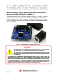
User's Guide
SLAU643 – July 2015
DRV10963 Evaluation Module
This document is provided with the DRV10963 customer evaluation module (EVM) as a supplement to the
DRV10963 datasheet (SLAS955A). It details the hardware implementation of the EVM and gives a stepby-step introduction to the device operation and tuning process using DRV10963 GUI.
1
2
3
4
5
6
7
Contents
DRV10963 EVM Kit Contents .............................................................................................. 2
Introduction ................................................................................................................... 3
DRV10963 Motherboard Connectors ..................................................................................... 4
3.1
Power Input .......................................................................................................... 4
3.2
Interface Connectors to Mount Daughterboard P1, P2 ........................................................ 4
3.3
USB to Any Connector ............................................................................................. 5
DRV10963 Daughterboard Connectors ................................................................................... 5
4.1
Motor Output Connector ........................................................................................... 5
4.2
Interface Connectors to Motherboard P1, P2 ................................................................... 5
Quick Start Guide ............................................................................................................ 6
5.1
Installation of Software ............................................................................................. 6
5.2
Initial Hardware Settings ........................................................................................... 6
5.3
Jumpers and Switch Setup Settings ............................................................................. 7
5.4
Powering-Up EVM .................................................................................................. 7
5.5
Tuning GUI: to Configure Motor Parameter ..................................................................... 8
Tuning Guide................................................................................................................ 13
6.1
Configuring the Device ........................................................................................... 13
6.2
Writing to the OTP Registers .................................................................................... 16
6.3
Reading the OTP Values ......................................................................................... 18
6.4
Notes ................................................................................................................ 18
Schematic and Bill of Materials ........................................................................................... 20
7.1
Schematic .......................................................................................................... 20
7.2
Bill of Materials (BOM) ............................................................................................ 22
List of Figures
1
DRV10963 Motherboard with Socket Daughterboard Mounted on top ............................................... 3
2
DRV10963 Daughterboard Mounting on Motherboard
3
4
5
6
7
8
9
10
11
12
13
14
................................................................. 6
DRV10963 Orientation Inside Daughterboard Socket .................................................................. 7
GUI Initial Screen With Demo Mode ..................................................................................... 8
GUI Screen With Successful I2C Interface .............................................................................. 9
Default Configuration Parameters ........................................................................................ 10
Loading DRV10963JM Configuration Parameter to Device .......................................................... 11
DRV10963JM Configuration Parameter ................................................................................ 12
Initial Tuning Flow Chart................................................................................................... 12
Error Message .............................................................................................................. 13
Correct Align Time and Acceleration Rate .............................................................................. 14
Align Time Too Long ....................................................................................................... 14
Align Time Too Short ...................................................................................................... 14
Open to Close Loop Threshold Too Low................................................................................ 14
SLAU643 – July 2015
Submit Documentation Feedback
DRV10963 Evaluation Module
Copyright © 2015, Texas Instruments Incorporated
1
DRV10963 EVM Kit Contents
www.ti.com
15
Open to Close Loop Threshold Too High ............................................................................... 14
16
Current Limit Too High
17
Current Limit Very Small
18
19
20
21
22
23
....................................................................................................
..................................................................................................
Load Custom Configurations to GUI .....................................................................................
Motor Hitting Current Limit and Trying Again ...........................................................................
OTC Threshold not Optimized ............................................................................................
Register Error Message ...................................................................................................
DRV10963 Motherboard Schematic .....................................................................................
DRV10963 Daughterboard Schematic ..................................................................................
15
15
17
18
18
19
20
21
List of Tables
1
1
Connector P1: Daughterboard ............................................................................................. 4
2
Connector P2: Daughterboard ............................................................................................. 4
3
Connector P1: Motherboard ................................................................................................ 5
4
Connector P2: Motherboard ................................................................................................ 5
5
DRV10963 Motherboard Bill of Materials ............................................................................... 22
6
DRV10963 Daughterboard Bill of Materials............................................................................. 23
DRV10963 EVM Kit Contents
The DRV10963 evaluation kit contains following:
1. DRV10963 motherboard circuit card
2. DRV10963 daughterboard circuit card
3. USB2ANY communication board for I2C GUI interaction
4. USB cable
5. 10-pin ribbon cable to connect USB2ANY and DRV10963 motherboard
6. DRV10963 EVM GUI
The DRV10963 EVM boards and GUI are designed to work together for tuning device to optimize the
performance for a given application.
2
DRV10963 Evaluation Module
SLAU643 – July 2015
Submit Documentation Feedback
Copyright © 2015, Texas Instruments Incorporated
Introduction
www.ti.com
2
Introduction
The DRV10963 EVM is an evaluation platform for the DRV10963 5-V three phase sensor-less BLDC
motor driver. The EVM is a combination of a motherboard and daughterboard. The motherboard includes
a TLC555 timer configured to supply a PWM to the DRV10963 and a potentiometer to adjust the speed of
the motor by varying the duty cycle of the PWM and has USB2ANY connector to communicate with
DRV10963 GUI. The daughterboard contains a socket allowing the device to be programmed using the
DRV10963 GUI via I2C communication and it is mounted on top motherboard, as shown in Figure 1. The
EVM set-up, together with DRV10963 GUI also provides means to program OTP (one time
programmable) of DRV10963 blank version (un-programmed OTP) device for any custom motor solution.
The DRV10963 GUI is easy to use, requires only four simple steps to tune the motor for any end
application and program the device OTP. The DRV10963 EVM comes with blank version device with unprogrammed OTP bits. The DRV10963 device has configurable shadow registers corresponding to each
OTP bit. Shadow registers provide ease-of-tuning to the user, as their values can be changed indefinitely
during the course of tuning to arrive at the best optimized values. The DRV10963 also has an I2C
interface, this allows the user to program specific motor parameters in shadow registers, before deciding
on final values to program OTP. Note that configurable shadow registers are volatile and lose their values
in power off condition.
This document describes the kit details and explains the functions and locations of test points, jumpers,
and connectors present on the kit. This document is also a quick start guide for using the GUI to tune a
motor for an end application. For detailed information about the DRV10963, refer to the DRV10963 data
sheet (SLAS955A).
Figure 1. DRV10963 Motherboard with Socket Daughterboard Mounted on top
SLAU643 – July 2015
Submit Documentation Feedback
DRV10963 Evaluation Module
Copyright © 2015, Texas Instruments Incorporated
3
DRV10963 Motherboard Connectors
www.ti.com
3
DRV10963 Motherboard Connectors
3.1
Power Input
The DRV 10963 requires two external power supply levels (6.2 V and 5 V) to operate the GUI via the I2C
interface. Connector P3 provides the required interface for external power supply. The pin assignment of
terminal P1 is as follows:
3.2
Pin
Description
1
GND
2
GND
3
Vtestmode-6.2 V to 7.2 V
3
Vpower-in-5.0 V to 6.0 V
Interface Connectors to Mount Daughterboard P1, P2
Connectors P1,P2 are used to interface the daughter socket board. The pin assignments are as follows:
Table 1. Connector P1: Daughterboard
Pin
Description
1, 2
NC
3
FR- Dual functionality:
1. Forward reverse for motor direction
2. Data signal for I2C
4
PWM, Dual functionality:
1. Motor speed control
2. Clock signal for I2C
5
FGS- Motor speed indicator selector
6
FG- Motor speed indicator output (open drain)
7
TOSC- To enable OTP programming
8, 9, 10, 11
NC
Table 2. Connector P2: Daughterboard
Pin
Description
1,2
VCC- 5-Volt power input
3
Phase-W
6, 7
Phase-U
8, 9
Phase-V
10, 11
4
NC
4, 5
GND
DRV10963 Evaluation Module
SLAU643 – July 2015
Submit Documentation Feedback
Copyright © 2015, Texas Instruments Incorporated
DRV10963 Motherboard Connectors
www.ti.com
3.3
USB to Any Connector
The Connector USB2ANY is used for the I2C interconnection with the GUI. The pin assignment is as
follows:
Pin
1, 2, 3, 4, 5
Description
NC
6
GND
7
NC
8
FGS Control- For Internal Factory Testing
9
SCLK- Clock signal for I2C communication with GUI
10
SDATA- Data signal for I2C communication with GUI
4
DRV10963 Daughterboard Connectors
4.1
Motor Output Connector
The DRV10963 daughterboard provides the 3-terminal connector P3 to connect 3-phase BLDC motor. Pin
assignment of terminal P3 is as follows:
Pin
4.2
Description
1
U
2
W
3
V
Interface Connectors to Motherboard P1, P2
Connectors P1,P2 are used to interface signals coming from the motherboard to the device via socket.
The pin assignments are as follows:
Table 3. Connector P1: Motherboard
Pin
Description
1, 2
NC
3
FR- Dual functionality:
1. Forward reverse for motor direction
2. Data signal for I2C
4
PWM, Dual functionality:
1. Motor speed control
2. Clock signal for I2C
5
FGS- Motor speed indicator selector
6
FG- Motor speed indicator output (open drain)
7
TOSC- To enable OTP programming
Table 4. Connector P2: Motherboard
Pin
Description
1, 2
VCC- 5-Volt power input
3
NC
4, 5
Phase-W
6, 7
Phase-U
8, 9
Phase-V
10, 11
GND
SLAU643 – July 2015
Submit Documentation Feedback
DRV10963 Evaluation Module
Copyright © 2015, Texas Instruments Incorporated
5
Quick Start Guide
www.ti.com
5
Quick Start Guide
5.1
Installation of Software
If this your first encounter with the DRV10963, before proceeding to next step, install the following
software packages to use the DRV10963 GUI for tuning the motor:
1. The DRV10963 EVM is provided with a GUI to configure the device and tune the application. Refer to
DRV10963_2P0 User Manual.pdf present (C:\Program Files (x86)\Texas Instruments\DRV10963_2P0
EVM\Documents) in the GUI-installed directory for instructions to download and install the GUI
application. Create a desktop shortcut with the name DRV10963_2P0 EVM, for future use.
2. Install the Run-Time Engine LabVIEW-2014 from the following link, for complete instructions, refer to
http://www.ni.com/download/labview-run-time-engine-2014/4887/en
CAUTION
Do not apply power to board before you have verified settings mentioned in
Section 5.2 and Section 5.3!
5.2
Initial Hardware Settings
The kit ships with the daughterboard already mounted on top of the motherboard. The daughter socket
board also has a pre-inserted DRV0963 blank version device, however, ensure:
• The daughterboard is rigidly inserted on the motherboard without any loose connection. Check the
orientation of the daughterboard with VCC_IN test-point connected to the right corner. Refer to
Figure 2 for details and read instructions written on the motherboard for proper orientation.
• The DRV10963 device is properly inserted with right orientation at the socket in the daughter card as
per Figure 3, referred to as U1.
:
VCC_IN Test Point of Daughter-Board
Figure 2. DRV10963 Daughterboard Mounting on Motherboard
6
DRV10963 Evaluation Module
SLAU643 – July 2015
Submit Documentation Feedback
Copyright © 2015, Texas Instruments Incorporated
Quick Start Guide
www.ti.com
Figure 3. DRV10963 Orientation Inside Daughterboard Socket
5.3
Jumpers and Switch Setup Settings
On the daughterboard:
1. Make sure that only jumper J1 is populated, jumper J2 and J3 all 3-pins shall be open
On motherboard:
1. Make sure that all jumpers J1, J2, and J3 are populated
2. Switch S1 should be in the off position and switch S2 in the I2C-GUI position. DRV10963 PWM input
pin has dual functionality, that is, it serves as speed control input as well as clock signal for I2C. Switch
S2 provides a means to configure the PWM input pin for speed control or I2C clock.
5.4
Powering-Up EVM
DRV10963 EVM requires two power supply sources, that is, 5 V and 6.2 V to work with the GUI to enable
I2C interface for register configuration. Note that programmed device needs only one 5-V supply in the
final end-application circuit. Use the following sequence to power-up the EVM and to establish a
successful connection with the GUI:
1. Do not power up the power supply. First, connect the power supply ground to pin GND, the 6.2 V to
pin V_Testmode, and 5 V to PowerIn on the motherboard at connector P3. At this point, make sure
that switch S1 is in the turn-off position and the “USB2Any” board is not connected to the motherboard.
If using a lab power supply, it is recommended to set the current limit of both power supplies to 1.5 A.
2. Turn the POT-R17 fully CCW (counter-clock wise). This keeps the speed PWM input to the minimum
value.
3. Connect the 3-phase terminal of motor to connector P4 on the daughterboard. It is not important to
observe the polarity as it only determines the direction of rotation.
4. Now power up the board and turn switch S1 to the “on” position. Check LED1, LED2, and LED3. All
should turn green.
5. Connect USB2Any box first, via the supplied USB cable to the computer. Then connect the 10-pin
ribbon cable to the USB2ANY connector on the motherboard.
SLAU643 – July 2015
Submit Documentation Feedback
DRV10963 Evaluation Module
Copyright © 2015, Texas Instruments Incorporated
7
Quick Start Guide
5.5
www.ti.com
Tuning GUI: to Configure Motor Parameter
Use the following steps to configure the motor parameters.
1. Now launch the DRV10963EVM GUI by double clicking the DRV10963_2P0 EVM shortcut on the
desktop. If "Demo Mode" is selected, the screen shown in Figure 4 appears, deselect "Demo Mode" to
go to the next step.
Figure 4. GUI Initial Screen With Demo Mode
2. If "Demo Mode" is not select previously, the screen shown in Figure 5 appears as soon as the GUI
launches. The "CONNECTED" block should turn green indicating that the GUI is successfully
connected to USB2ANY.
8
DRV10963 Evaluation Module
SLAU643 – July 2015
Submit Documentation Feedback
Copyright © 2015, Texas Instruments Incorporated
Quick Start Guide
www.ti.com
Figure 5. GUI Screen With Successful I2C Interface
3. Left-click on the step 1 button “Set Default Resister Values”. Step 1 is always mandatory before
proceeding to step 2 to enable configuration of the device. This step programs the following
parameters to the corresponding shadow register, as shown in Figure 6. These default values
correspond to the factory programmed part DRV10963JJ. Refer to the DRV10963 datasheet for a
detailed explanation of different versions of DRV10963 and descriptions of tunable parameters.
• "Start Up Align Time" - 350 ms and "Start-up Acceleration Rate" - 80 Hz/s
• "Open to Close Loop Threshold" - 100 Hz
• "PWM Duty Cycle Cutoff" - 10%
• "FG Frequency Divider" - 1 or 1/3
• "Software Current limit" - 500 mA
• "Voltage Delay" - 120 µs
To enable motor spin with the above parameters, open the jumper J1 on the motherboard. There is a
high probability that the motor will start rotating with previously shown default values. This state is
equivalent to driving the motor at maximum speed with 100% duty cycle because PWM input being
connected to the I2C clock input continues to receive a high signal. Ensure that the parameters
previously shown are optimized for their end application. Refer to Section 6 for guidelines to optimally
determine and tune motor parameters using the GUI.
SLAU643 – July 2015
Submit Documentation Feedback
DRV10963 Evaluation Module
Copyright © 2015, Texas Instruments Incorporated
9
Quick Start Guide
www.ti.com
Figure 6. Default Configuration Parameters
4. To facilitate the tuning at different speeds or across a speed range, the EVM provides a TLC555 timerbased PWM generation circuit and potentiometer (R17) to adjust the duty cycle of PWM to control the
speed of the motor. To enable speed control via POT-R17, change the switch S2 position to PWM
Speed Control mode. Turn the POT-R17 clock-wise to increase the motor speed and counterclockwise to reduce it.
5. In case motor performance is not satisfactory with default values or further optimization is desired, try
three other factory-programmed device options before attempting to customize parameters. This would
benefit in production phase because all versions of factory programmed devices can be easily
procured and used directly without the burden to programming the OTP values. The GUI comes with
three .txt files corresponding to the three remaining factory-programmed devices.
6. To test motor performance with the DRV10963JM version, short the jumper J1 back. This will stop the
motor. Referring to Figure 7, left-click the “Load Config“ button, browse to the GUI installation directory
for 3 .txt files in your PC and select DRV10963JM.txt.This will load the register with configuration
parameters corresponding to DRV10963JM. Refer to Figure 8 to check configuration parameters
corresponding to the DRV10963JM version. In same way, load and configure other versions of
DRV10963 to test the performance. To enable motor spin, open the jumper J1 on the motherboard and
use POT R-17 for speed control.
10
DRV10963 Evaluation Module
SLAU643 – July 2015
Submit Documentation Feedback
Copyright © 2015, Texas Instruments Incorporated
Quick Start Guide
www.ti.com
Figure 7. Loading DRV10963JM Configuration Parameter to Device
SLAU643 – July 2015
Submit Documentation Feedback
DRV10963 Evaluation Module
Copyright © 2015, Texas Instruments Incorporated
11
Quick Start Guide
www.ti.com
Figure 8. DRV10963JM Configuration Parameter
7. After trying DRV10963JM, the next file to load is the DRV10963JU configuration followed by loading
the DRV10963JA.
8. If only one of the preloaded configurations spins the motor, then obviously that is the part number to
order to control the motor. However, if two or more spin the motor, then refer to Figure 9.
Figure 9. Initial Tuning Flow Chart
12
DRV10963 Evaluation Module
SLAU643 – July 2015
Submit Documentation Feedback
Copyright © 2015, Texas Instruments Incorporated
Tuning Guide
www.ti.com
9. Even if one of the four factory-programmed settings do spin the motor, it may not be optimized for that
motor. Using whichever DRV10963xx file as a starting point, then run through the tuning guide in
Section 6 to create the best settings. However, for convenience it would be easier to just order a
factory-programmed part. The "Control Advance Angle Method is described in Section 6.1.6.
6
Tuning Guide
If all four of the given factory-programmed settings have been tried (3 .txt files and the default values) and
the motor still will not spin or you would like to further optimize your motor then you can try the following
steps to custom tune the DRV10963 for your motor.
6.1
Configuring the Device
Leave the device connected to the motor and the computer. Next, make sure that the DRV10963EVM is
powered up in test mode and the GUI is open. If an error message like the one in Figure 10 is returned,
just close the GUI and reopen it and make sure that it reconnects to the device.
Figure 10. Error Message
Each one of the parameters that you can configure with the GUI will change how your motor reacts to the
DRV10963 device. Read the description of each one of the parameters below and then choose if you
would like to make the changes suggested. Be sure to connect a current probe to phase V to observe the
phase current during tuning.
6.1.1
Start UP Align Time and Start Up Acceleration Rate
Start-up align time and acceleration rate determines how fast the motor can reach a particular set speed
from standstill, so these values should be chosen to get the fastest possible start-up time. Note that too
aggressive values of acceleration rate can cause higher inrush current in starting and may hit overcurrent
protection, in which case the motor may not be able to start successfully. It is better to start with slower
values and gradually increases to get the fastest possible start-up time based on the application. In the
DRV10963 device, both the values are dependent on each other. They can only be configured as a
dependent pair. The values tunable from the GUI of align time is in ms and acceleration rate is in Hz/sec.
Using the motor inertia from the motor parameters previously determined, estimate the align time. If you
do not know, just input the highest possible align time which will correspond to the lowest possible
acceleration rate. Then, after tuning the rest of the parameters is complete, come back to align time and
step it down one-by-one until the fan will not spin. Then you know the best align time is the value just
before the one where the fan stopped.
SLAU643 – July 2015
Submit Documentation Feedback
DRV10963 Evaluation Module
Copyright © 2015, Texas Instruments Incorporated
13
Tuning Guide
www.ti.com
Figure 11. Correct Align Time and Acceleration Rate
Figure 12. Align Time Too Long
6.1.2
Figure 13. Align Time Too Short
Open to Close Loop Threshold
Open to close loop threshold determines the threshold frequency at which the controller goes from openloop commutation to closed-loop, back-emf, zero-crossing-based commutation. For best performance to
get stability during dynamic load/speed changing conditions and for maximum possible speed range, the
motor should run in closed-loop commutation mode, therefore, the threshold frequency should be chosen
as low as possible. However, too low values will cause an issue with sensor-less control because backemf will not be sufficient to allow closed loop operation. Typically this threshold should be 10% to 25% of
the speed desired to run the motor. The values tunable via GUI are in units of Hz. Normally, higher-speed
motors (maximum speed) require a higher handoff threshold because higher speed motors have lower Kt,
and as a result, lower BEMF.
In other words, if your desired RPM is 3000, then the open to close loop threshold should be 1/4 × (500
rpm) = 125 Hz. Therefore, the open to close loop threshold should be around 50≈125 Hz.
14
DRV10963 Evaluation Module
SLAU643 – July 2015
Submit Documentation Feedback
Copyright © 2015, Texas Instruments Incorporated
Tuning Guide
www.ti.com
Figure 14. Open to Close Loop Threshold Too Low
6.1.3
Figure 15. Open to Close Loop Threshold Too High
PWM Duty Cycle Cutoff
PWM duty cycle cutoff decides the minimum operating duty cycle; this can be chosen to meet minimum
speed requirements. Refer to the DRV10963 datasheet for more information about the different minimum
duty cycles.
6.1.4
FG Frequency Divider
The FG pin provides an indication of the speed of the motor. There are two options, 1 or 1/2 toggles FG
once every 2 electrical cycles and 1 or 1/3, toggles FG once every 3 electrical cycles. This signal can be
used to get the motor speed feedback information. In order to see this relationship off of the FG pin on the
daughterboard, the device must be taken out of test mode by opening the jumper J1 on the motherboard,
using the POT R-17 for speed control, and the FGS pin must be driven low. For more information about
this, refer to the DRV10963 datasheet.
6.1.5
Software Current Limit
The software current limit function is only available in closed loop commutation mode. It works more like
an active current or better as torque limit, and does not cause overcurrent trip. This value can tune to get
a particular speed at a given motor loading condition. For example, increasing its value increases the
motor-applied torque and thus the speed, however, ensure that the value is not exuberantly high to
prevent motor heating. A lower value will prevent the motor from reaching a higher speed.
Start out at 0.125 A to make sure that your motor will spin and then slowly start to increase the current
limit until it fails, then use the current limit right before.
Figure 16. Current Limit Too High
Figure 17. Current Limit Very Small
SLAU643 – July 2015
Submit Documentation Feedback
DRV10963 Evaluation Module
Copyright © 2015, Texas Instruments Incorporated
15
Tuning Guide
6.1.6
www.ti.com
Control Advance Angle Method a.k.a Voltage Delay
Voltage delay represents lagging phase angle (in unit of time) of back-emf with respect to applied voltage.
As explained in the datasheet, for efficient operation, applied voltage must lead the back-emf to force the
motor-current in phase with back-emf for constant air-gap BLDC moor without saliency. For salient pole
motors back-emf and phase current may have phase angle difference for efficient operation depending
upon motor parameters. Both types of motor can be tuned efficiently via the GUI using voltage delay. In
the GUI, zero delay setting forces the applied voltage in phase with back-emf and increasing its value,
make the applied voltage to lead with respect to back-emf. To determine the optimized value, run the
motor at rated speed as per end-application requirement and adjust the value to draw minimum current
from the power supply.
1. Configure the motor using the Tuning Guide up to this point and make sure it can spin in closed loop
control (after the current flat lines on startup and then keeps oscillating). Switch S2 to the PWM so it
can receive a PWM signal. Have a current probe on one of the phases of the motor and a voltage
probe on the FG pin of the daughterboard. Also make sure that the input voltage VIN is run through a
multimeter so that you can know the exact output current at all times.
2. Change the Voltage Delay to “No Delay” and click ‘Configure Parameters’.
3. Next, the device must be taken out of test mode. Disconnect the USB2ANY from the EVM board. Turn
off the output of 6.2 V. Disconnect the J2 jumper from the motherboard.
4. Connect a function generator to the PWM in the pin located on the daughterboard. The function
generator is outputting 50 kHz square wave at 5 Vpp with 2.5 V DC offset and in High Z. Using this
signal, adjust the duty cycle to reach the RPM that is desired for your application. The RPM can be
obtained using Equation 1. The frequency of the FG pin corresponds to the electrical frequency.
ƒ elec
RPM =
´ 60
# of poles
(1)
5. Take the current measure from the multimeter.
6. Once you have those taken down, turn off the output of the function generator and do the steps in
reverse order to put the device back into test mode. Connect J2 and the USB2ANY and then turn on
the 6.2-V supply.
7. Reopen the GUI, connect to the device and set the default register values like in the tuning guide.
Next, configure all other values to what they were when the motor was spinning in closed loop.
8. Repeat Steps 2-7 several times changing the "Voltage Delay" each time to get a few reference points.
9. The "Voltage Delay" value that has the smallest current off of the multimeter is the current that is most
in phase with the BEMF.
If you are deciding between the JA and the JJ models, just do Steps 4 and 5 for both parts and pick the
one with the minimum current between the two.
6.2
Writing to the OTP Registers
Each time when writing to the OTP registers, always ensure:
Jumper J1 on motherboard remains:
Shorted to enable I2C and configuration via GUI
Open to enable motor spin after any configuration
Switch S2 on motherboard remains:
I2C-GUI to enable I2C and configuration via GUI
"Speed Control" mode to enable PWM to device
1. The EVM provides means to program the OTPs of a blank part. To enable OTP programming of any
new blank device:
• Disconnect the motor from EVM
• Start with initial condition of jumpers/switches mentioned in Section 5.3 and follow-up power on
EVM steps of Section 5.4.
2. As a first step to program the OTP, launch the GUI and left click "Set Default Register Value", that is,
step 1. Load the custom configuration as shown in Figure 18 from the stored directory on your PC.
16
DRV10963 Evaluation Module
SLAU643 – July 2015
Submit Documentation Feedback
Copyright © 2015, Texas Instruments Incorporated
Tuning Guide
www.ti.com
Figure 18. Load Custom Configurations to GUI
3. Increase the V_Testmode voltage level to 7.4 V and Vpower_in to 6.2 V. Now, left click “Write OTP
Values” from the GUI. This will program the OTP bits of a blank device with user-configured values.
CAUTION
Never exceed Vpower_in beyond 6.5 V in any circumstances to prevent
damaging the EVM.
4. In order to ensure that OTP are programmed properly, step 4 provides a means for read-back option.
To enable read-back, first reduce the V_Testmode voltage level back to 6.2 V and Vpower_in to 5.0 V
and left click “Read OTP Values”. If the GUI does not give any error message, it ensures the correct
OTP programming. This means the device is ready to be used in stand-alone mode at the endapplication circuit.
5. The final test to ensure proper OTP programming, power down both power supplies, disconnect the
USB2ANY. Reconnect the motor to EVM and reapply 6.2 V and 5.0 V, don’t connect USB2ANY and
open the jumper J1 on motherboard. The motor will start rotating confirming that the OTP are
programmed and device is ready to use.
NOTE: The DRV10963 blank version is not available off-the-shelf for direct purchase, contact TI
sales or distributors for further details if custom settings for production with a blank version is
desired.
SLAU643 – July 2015
Submit Documentation Feedback
DRV10963 Evaluation Module
Copyright © 2015, Texas Instruments Incorporated
17
Tuning Guide
6.3
www.ti.com
Reading the OTP Values
After writing the values from the shadow register to the OTP, complete step four on the GUI and read
back the OTP values to make sure they are correct.
6.4
Notes
There are several issues that may occur when tuning the DRV1093 to your motor. The following sections
details several common issues that could happen and how to fix them.
6.4.1
Hitting Current Limit
If the beginning of the current waveform looks like Figure 19, there might be a problem with the current
limitation of the chip itself. If the align time is small, the current limit of the chip is reached and the chip
turns itself off, waits for a set amount of time then tries again. If you see a waveform like the one below
either add a 1-Ω resistor to each one of the 3 phases or lower the VIN to around 4.8 V.
Figure 19. Motor Hitting Current Limit and Trying Again
6.4.2
Open to Close Loop Threshold High
Sometimes even though the motor will go into closed loop at a certain threshold does not mean that it is
optimized. If the current waveform resembles the one shown in Figure 20 before it goes into closed loop (it
goes into closed loop after the flat line in the middle where the GUI is measuring the BEMF) then it means
that the Open to Closed Loop Threshold is high. This is an inefficient way to start up the motor because it
is dangerously close to hitting a current limit and stopping the motor waiting and trying again. The
optimized performance would be to make the current funnel down until it hits closed loop control.
Figure 20. OTC Threshold not Optimized
18
DRV10963 Evaluation Module
SLAU643 – July 2015
Submit Documentation Feedback
Copyright © 2015, Texas Instruments Incorporated
Tuning Guide
www.ti.com
6.4.3
Cannot Read Registers GUI Error
Sometimes when trying to "Set Default Register Values", the GUI will try to read the registers off of the
device and cannot do so. The GUI will then throw this error message.
Figure 21. Register Error Message
Click continue and try again to "Set Default Register Values". It should work the second time, if all of the
connections are correct from the Quick Start Guide in Section 5. If not, just power cycle the EVM and
restart the GUI.
SLAU643 – July 2015
Submit Documentation Feedback
DRV10963 Evaluation Module
Copyright © 2015, Texas Instruments Incorporated
19
Schematic and Bill of Materials
7
www.ti.com
Schematic and Bill of Materials
This section contains the DRV10983 schematic and bill of materials (BOM).
7.1
Schematic
Figure 22 shows the DRV10963 motherboard schematic.
Speed Control Section
Interface Connectors for Daughter Board
P1
FR
PWM
FGS
FG
TOSC
555 Timer as PWM Generator ~25kHz
USB to Any Connector
R16
P2
VCC
VCC
1
2
3
4
5
6
7
8
9
10
11
U
U
W
W
V
V
GND
GND
VCC
TP2 TP1 TP3
1
2
3
4
5
6
7
8
9
10
11
10.0k
P4
1
3
5
7
9
U
W
V
SCLK
2
4
6
8
10
U4
FGS_CNTL
SDATA
GND
4
RST
DIS
7
6
THR
OUT
3
2
TRIG
CVOLT
5
8
+VCC
GND
1
5103308-1
C8
0.01µF
PWM_Duty
C7
0.01µF
TLC555
D2
D1
C9
0.1µF
R17
P3
V TestMode= 6.2Volt
1
2
3
4
Vcc=5Volt
V_TESTMODE
U1
PowerIn
C4
10µF
TP6
C5
47µF
5K
VCC
TP7
VCC
TP4
C1
4.7µF
L1
1
VI
SW
5
3
EN
FB
4
GND
2
C2
10µF
V3P3
10µH
V3P3
I2C Communication
C3
10µF
V3P3
R9
4.7k
1
TPS62203DBV
V_TESTMODE
2
V3P3
R1
1.00k
S1
R12
100
R3
3.01k
R2
3.01k
PowerIn plus test mode entry
voltage Power
3
PWM_Duty
LED2
S2-3:
LED3
PWM
2
SCLK
C6
0.1µF
LED1
S2
1
VCC
3
S2-1: I2C communication with GUI
PWM duty cycle for speed control using POT
3
V3P3
FR_BUF
FR_BUF
TP9
TP11
TP12
4
2
5
GND
TP8
R10
4.7k
U2
TP13 TP14
SDATAR15
100
Must have a single point for bidirectional
MBRM110L
FR
TP16
3
Test Points for GND
FG_BUF
FG_BUF
U3
J2
2
FG
5
To Enable OTP programming Test Voltage
4
For Factory Testing
V_TESTMODE
J3
2
V3P3
V3P3
1.00k
R6
10.0k
Q2
R7
4.7k
J1
R8
10.0k
R11
1
3
R4
10.0k
R5
Q1
TOSC
R13
FGS_CNTL
10.0k
R14
4.7k
1.00k
Q3
FGS
Q4
Figure 22. DRV10963 Motherboard Schematic
20
DRV10963 Evaluation Module
SLAU643 – July 2015
Submit Documentation Feedback
Copyright © 2015, Texas Instruments Incorporated
Schematic and Bill of Materials
www.ti.com
Figure 23 shows the DRV10963 daughterboard schematic.
Interface connectors for Mother-Board
FR select
1
2
3
4
5
6
7
8
9
10
11
U
U
W
W
V
V
GND
GND
VCC
VCC
3
2
1
FR
PWMIN
FGS
FG
TOSC
FGS select
P2
VCC
VCC
3
2
1
P1
1
2
3
4
5
6
7
J2
J3
FGS
FR
VCC
J1
DRV10963 device with Socket
R1
100k
1
2
3
4
VCC_IN
GND
PWMIN
FG
1
2
P3
U1
FG
1
FGS
2
VCC
VCC
VCC
3
W
C1
10µF
C2
2.2µF
4
5
FG
FGS
Vcc
PWMIN
TOSC
FR
W
U
GND
V
PWMIN
10
TOSC
9
8
FR
7
U
6
V
To Motor Phases
U
W
V
1
2
3
P4
11
Test Points
PWMIN
PWMIN
VCC_IN
VCC_IN
VCC
VCC
FG
U
FG
FR
W
FR
V
U
GND
GND1
V
FGS
W
FGS
Figure 23. DRV10963 Daughterboard Schematic
SLAU643 – July 2015
Submit Documentation Feedback
DRV10963 Evaluation Module
Copyright © 2015, Texas Instruments Incorporated
21
Schematic and Bill of Materials
7.2
www.ti.com
Bill of Materials (BOM)
Table 5 lists the DRV10963 motherboard bill of materials.
Table 5. DRV10963 Motherboard Bill of Materials
Item #
Designator
Qty
1
!PCB
1
2
C1
1
3
C2, C3, C4
3
4
C5
5
PartNumber
Manufacturer
Description
MDBU001
Any
Printed Circuit Board
4.7uF
GRM21BR61C475KA88L
Murata
CAP, CERM, 4.7uF, 16V, +/-10%, X5R, 0805
0805
10uF
GRM21BR61C106KE15L
Murata
CAP, CERM, 10uF, 16V, +/-10%, X5R, 0805
0805
1
47uF
GRM32ER61C476KE15L
Murata
CAP, CERM, 47uF, 16V, +/-10%, X5R, 1210
1210
C6, C9
2
0.1uF
GRM155R71A104KA01D
Murata
CAP, CERM, 0.1uF, 10V, +/-10%, X7R, 0402
0402
6
C7, C8
2
0.01uF
C0805C103K1RACTU
Kemet
CAP, CERM, 0.01 µF, 100 V, +/- 10%, X7R, 0805
0805
7
D1, D2
2
40V
MSS1P4-M3/89A
Vishay-Siliconix
Diode, Schottky, 40 V, 1 A, MicroSMP
MicroSMP
8
FG_BUF, FR_BUF,
GND, TP1, TP2,
TP3, TP4, TP6,
TP7, TP8, TP9,
TP11, TP12, TP13,
TP14, TP16, V3P3
17
SMT
5015
Keystone
Test Point, Miniature, SMT
Testpoint_Keystone_Miniature
9
FID1, FID2, FID3
3
N/A
N/A
Fiducial mark. There is nothing to buy or mount.
Fiducial
10
H1, H2, H3, H4
4
SJ-5303 (CLEAR)
3M
Bumpon, Hemisphere, 0.44 X 0.20, Clear
Transparent Bumpon
11
J1, J2, J3
3
PBC02SAAN
Sullins Connector Solutions
Header, 100mil, 2x1, Gold, TH
Sullins 100mil, 1x2, 230 mil above insulator
12
L1
1
CDRH5D18NP-100NC
Sumida
Inductor, Shielded Drum Core, Ferrite, 10uH, 1.2A,
0.124 ohm, SMD
CDRH5D18
13
LED1, LED2, LED3
3
LTST-C171GKT
Lite-On
LED, Green, SMD
LED_0805
14
P1, P2
2
BCS-111-L-S-PE
Samtec
Receptacle, 2.54mm, 11x1, Gold, TH
Receptacle, 2.54mm, 11x1, TH
15
P3
1
ED555/4DS
On-Shore Technology
Terminal Block, 6A, 3.5mm Pitch, 4-Pos, TH
14x8.2x6.5mm
16
P4
1
5103308-1
TE Connectivity
Header (shrouded), 100mil, 5x2, Gold, TH
5x2 Shrouded header
17
PCB2
1
Used in BOM report
Used in BOM report
Will add component to BOM. Useful for cables, nuts,
etc. not in libraries
Used in PnP output and some BOM reports
18
Q1, Q3
2
0.25V
MMBT3906
Fairchild Semiconductor
Transistor, PNP, 40V, 0.2A, SOT-23
SOT-23
19
Q2, Q4
2
0.2V
MMBT3904
Fairchild Semiconductor
Transistor, NPN, 40V, 0.2A, SOT-23
SOT-23
20
R1, R5, R11
3
1.00k
CRCW06031K00FKEA
Vishay-Dale
RES, 1.00k ohm, 1%, 0.1W, 0603
0603
21
R2, R3
2
3.01k
CRCW06033K01FKEA
Vishay-Dale
RES, 3.01k ohm, 1%, 0.1W, 0603
0603
22
R4, R6, R8, R13
4
10.0k
CRCW060310K0FKEA
Vishay-Dale
RES, 10.0k ohm, 1%, 0.1W, 0603
0603
23
R7, R9, R10, R14
4
4.7k
CRCW06034K70JNEA
Vishay-Dale
RES, 4.7k ohm, 5%, 0.1W, 0603
0603
24
R12, R15
2
100
RC0603FR-07100RL
Yageo America
RES, 100 ohm, 1%, 0.1W, 0603
0603
25
R16
1
10.0k
CRCW080510K0FKEA
Vishay-Dale
RES, 10.0 k, 1%, 0.125 W, 0805
0805
26
R17
1
5K
296UD502B1N
CTS Electrocomponents
Trimmer, 5K Ohms, 0.15 W, TH
TH, 3-Leads, Body 12.5x12.8mm, Height
23.2mm
27
S1
1
100SP1T1B4M2QE
E-Switch
Switch, SPDT, On-On, 2 Pos, TH
12.7x6.86mm
28
S2
1
500SSP1S2M2QEA
E-Switch
Switch, SPDT, Slide, On-On, 2 Pos, TH
12.85x6.6mm
22
Value
10uH
DRV10963 Evaluation Module
PackageReference
SLAU643 – July 2015
Submit Documentation Feedback
Copyright © 2015, Texas Instruments Incorporated
Schematic and Bill of Materials
www.ti.com
Table 5. DRV10963 Motherboard Bill of Materials (continued)
Item #
Designator
Qty
Value
PartNumber
Manufacturer
Description
PackageReference
29
SH-J1, SH-J2, SHJ3
3
1x2
SPC02SYAN
Sullins Connector Solutions
Shunt, 100mil, Flash Gold, Black
Closed Top 100mil Shunt
30
U1
1
TPS62203DBVR
Texas Instruments
HIGH-EFFICIENCY, STEP-DOWN, DC-DC
CONVERTER, DBV0005A
DBV0005A
31
U2, U3
2
SN74LVC1G17DCKR
Texas Instruments
SINGLE SCHMITT-TRIGGER BUFFER, DCK0005A
DCK0005A
32
U4
1
TLC555CDR
Texas Instruments
Timer, 8-pin Narrow SOIC
M08A
Table 6 lists the DRV10963 daughterboard bill of materials.
Table 6. DRV10963 Daughterboard Bill of Materials
Item # Designator
Qty
1
!PCB
1
2
C1
1
3
C2
1
4
FG, FGS, FR,
GND, GND1,
PWMIN, U, V,
VCC, VCC_IN, W
11
5
FID1, FID2, FID3,
FID4, FID5, FID6
6
7
Value
PartNumber
Manufacturer
Description
MDBU002
Any
Printed Circuit Board
10uF
GRM21BR61C106KE15L
Murata
CAP, CERM, 10uF, 16V, +/-10%, X5R, 0805
0805
2.2uF
GRM188R61C225KE15D
Murata
CAP, CERM, 2.2uF, 16V, +/-10%, X5R, 0603
0603
SMT
5015
Keystone
Test Point, Miniature, SMT
Testpoint_Keystone_Miniature
6
N/A
N/A
Fiducial mark. There is nothing to buy or mount.
Fiducial
J1
1
PBC02SAAN
Sullins Connector Solutions
Header, 100mil, 2x1, Gold, TH
Sullins 100mil, 1x2, 230 mil above insulator
J2, J3
2
PEC03SAAN
Sullins Connector Solutions
Header, 100mil, 3x1, Tin, TH
Header, 3 PIN, 100mil, Tin
8
P1
1
PBC07SAAN
Sullins Connector Solutions
Header, 2.54 mm, 7x1, Gold, TH
Header, 2.54 mm, 7x1, TH
9
P2
1
PBC11SAAN
Sullins Connector Solutions
Header, 2.54 mm, 11x1, Gold, TH
Header, 2.54 mm, 11x1, TH
10
P3
1
PBC04SAAN
Sullins Connector Solutions
Header, 2.54 mm, 4x1, Gold, TH
Header, 2.54 mm, 4x1, TH
11
P4
1
1x3
PBC03SAAN
Sullins Connector Solutions
Header, 100mil, 3x1, Gold, TH
PBC03SAAN
12
R1
1
100k
RC0603FR-07100KL
Yageo America
RES, 100k ohm, 1%, 0.1W, 0603
0603
13
SH-J1, SH-J2, SHJ3
3
1x2
SPC02SYAN
Sullins Connector Solutions
Shunt, 100mil, Flash Gold, Black
Closed Top 100mil Shunt
14
U1
1
QFN-10(20)B-0.5-02
Enplas Tech Solutions
Socket, QFN-10, 0.5mm pitch, TH
Socket, QFN-10, 0.5mm Pitch
SLAU643 – July 2015
Submit Documentation Feedback
PackageReference
DRV10963 Evaluation Module
Copyright © 2015, Texas Instruments Incorporated
23
STANDARD TERMS AND CONDITIONS FOR EVALUATION MODULES
1.
Delivery: TI delivers TI evaluation boards, kits, or modules, including any accompanying demonstration software, components, or
documentation (collectively, an “EVM” or “EVMs”) to the User (“User”) in accordance with the terms and conditions set forth herein.
Acceptance of the EVM is expressly subject to the following terms and conditions.
1.1 EVMs are intended solely for product or software developers for use in a research and development setting to facilitate feasibility
evaluation, experimentation, or scientific analysis of TI semiconductors products. EVMs have no direct function and are not
finished products. EVMs shall not be directly or indirectly assembled as a part or subassembly in any finished product. For
clarification, any software or software tools provided with the EVM (“Software”) shall not be subject to the terms and conditions
set forth herein but rather shall be subject to the applicable terms and conditions that accompany such Software
1.2 EVMs are not intended for consumer or household use. EVMs may not be sold, sublicensed, leased, rented, loaned, assigned,
or otherwise distributed for commercial purposes by Users, in whole or in part, or used in any finished product or production
system.
2
Limited Warranty and Related Remedies/Disclaimers:
2.1 These terms and conditions do not apply to Software. The warranty, if any, for Software is covered in the applicable Software
License Agreement.
2.2 TI warrants that the TI EVM will conform to TI's published specifications for ninety (90) days after the date TI delivers such EVM
to User. Notwithstanding the foregoing, TI shall not be liable for any defects that are caused by neglect, misuse or mistreatment
by an entity other than TI, including improper installation or testing, or for any EVMs that have been altered or modified in any
way by an entity other than TI. Moreover, TI shall not be liable for any defects that result from User's design, specifications or
instructions for such EVMs. Testing and other quality control techniques are used to the extent TI deems necessary or as
mandated by government requirements. TI does not test all parameters of each EVM.
2.3 If any EVM fails to conform to the warranty set forth above, TI's sole liability shall be at its option to repair or replace such EVM,
or credit User's account for such EVM. TI's liability under this warranty shall be limited to EVMs that are returned during the
warranty period to the address designated by TI and that are determined by TI not to conform to such warranty. If TI elects to
repair or replace such EVM, TI shall have a reasonable time to repair such EVM or provide replacements. Repaired EVMs shall
be warranted for the remainder of the original warranty period. Replaced EVMs shall be warranted for a new full ninety (90) day
warranty period.
3
Regulatory Notices:
3.1 United States
3.1.1
Notice applicable to EVMs not FCC-Approved:
This kit is designed to allow product developers to evaluate electronic components, circuitry, or software associated with the kit
to determine whether to incorporate such items in a finished product and software developers to write software applications for
use with the end product. This kit is not a finished product and when assembled may not be resold or otherwise marketed unless
all required FCC equipment authorizations are first obtained. Operation is subject to the condition that this product not cause
harmful interference to licensed radio stations and that this product accept harmful interference. Unless the assembled kit is
designed to operate under part 15, part 18 or part 95 of this chapter, the operator of the kit must operate under the authority of
an FCC license holder or must secure an experimental authorization under part 5 of this chapter.
3.1.2
For EVMs annotated as FCC – FEDERAL COMMUNICATIONS COMMISSION Part 15 Compliant:
CAUTION
This device complies with part 15 of the FCC Rules. Operation is subject to the following two conditions: (1) This device may not
cause harmful interference, and (2) this device must accept any interference received, including interference that may cause
undesired operation.
Changes or modifications not expressly approved by the party responsible for compliance could void the user's authority to
operate the equipment.
FCC Interference Statement for Class A EVM devices
NOTE: This equipment has been tested and found to comply with the limits for a Class A digital device, pursuant to part 15 of
the FCC Rules. These limits are designed to provide reasonable protection against harmful interference when the equipment is
operated in a commercial environment. This equipment generates, uses, and can radiate radio frequency energy and, if not
installed and used in accordance with the instruction manual, may cause harmful interference to radio communications.
Operation of this equipment in a residential area is likely to cause harmful interference in which case the user will be required to
correct the interference at his own expense.
SPACER
SPACER
SPACER
SPACER
SPACER
SPACER
SPACER
SPACER
FCC Interference Statement for Class B EVM devices
NOTE: This equipment has been tested and found to comply with the limits for a Class B digital device, pursuant to part 15 of
the FCC Rules. These limits are designed to provide reasonable protection against harmful interference in a residential
installation. This equipment generates, uses and can radiate radio frequency energy and, if not installed and used in accordance
with the instructions, may cause harmful interference to radio communications. However, there is no guarantee that interference
will not occur in a particular installation. If this equipment does cause harmful interference to radio or television reception, which
can be determined by turning the equipment off and on, the user is encouraged to try to correct the interference by one or more
of the following measures:
•
•
•
•
Reorient or relocate the receiving antenna.
Increase the separation between the equipment and receiver.
Connect the equipment into an outlet on a circuit different from that to which the receiver is connected.
Consult the dealer or an experienced radio/TV technician for help.
3.2 Canada
3.2.1
For EVMs issued with an Industry Canada Certificate of Conformance to RSS-210
Concerning EVMs Including Radio Transmitters:
This device complies with Industry Canada license-exempt RSS standard(s). Operation is subject to the following two conditions:
(1) this device may not cause interference, and (2) this device must accept any interference, including interference that may
cause undesired operation of the device.
Concernant les EVMs avec appareils radio:
Le présent appareil est conforme aux CNR d'Industrie Canada applicables aux appareils radio exempts de licence. L'exploitation
est autorisée aux deux conditions suivantes: (1) l'appareil ne doit pas produire de brouillage, et (2) l'utilisateur de l'appareil doit
accepter tout brouillage radioélectrique subi, même si le brouillage est susceptible d'en compromettre le fonctionnement.
Concerning EVMs Including Detachable Antennas:
Under Industry Canada regulations, this radio transmitter may only operate using an antenna of a type and maximum (or lesser)
gain approved for the transmitter by Industry Canada. To reduce potential radio interference to other users, the antenna type
and its gain should be so chosen that the equivalent isotropically radiated power (e.i.r.p.) is not more than that necessary for
successful communication. This radio transmitter has been approved by Industry Canada to operate with the antenna types
listed in the user guide with the maximum permissible gain and required antenna impedance for each antenna type indicated.
Antenna types not included in this list, having a gain greater than the maximum gain indicated for that type, are strictly prohibited
for use with this device.
Concernant les EVMs avec antennes détachables
Conformément à la réglementation d'Industrie Canada, le présent émetteur radio peut fonctionner avec une antenne d'un type et
d'un gain maximal (ou inférieur) approuvé pour l'émetteur par Industrie Canada. Dans le but de réduire les risques de brouillage
radioélectrique à l'intention des autres utilisateurs, il faut choisir le type d'antenne et son gain de sorte que la puissance isotrope
rayonnée équivalente (p.i.r.e.) ne dépasse pas l'intensité nécessaire à l'établissement d'une communication satisfaisante. Le
présent émetteur radio a été approuvé par Industrie Canada pour fonctionner avec les types d'antenne énumérés dans le
manuel d’usage et ayant un gain admissible maximal et l'impédance requise pour chaque type d'antenne. Les types d'antenne
non inclus dans cette liste, ou dont le gain est supérieur au gain maximal indiqué, sont strictement interdits pour l'exploitation de
l'émetteur
3.3 Japan
3.3.1
Notice for EVMs delivered in Japan: Please see http://www.tij.co.jp/lsds/ti_ja/general/eStore/notice_01.page 日本国内に
輸入される評価用キット、ボードについては、次のところをご覧ください。
http://www.tij.co.jp/lsds/ti_ja/general/eStore/notice_01.page
3.3.2
Notice for Users of EVMs Considered “Radio Frequency Products” in Japan: EVMs entering Japan may not be certified
by TI as conforming to Technical Regulations of Radio Law of Japan.
If User uses EVMs in Japan, not certified to Technical Regulations of Radio Law of Japan, User is required by Radio Law of
Japan to follow the instructions below with respect to EVMs:
1.
2.
3.
Use EVMs in a shielded room or any other test facility as defined in the notification #173 issued by Ministry of Internal
Affairs and Communications on March 28, 2006, based on Sub-section 1.1 of Article 6 of the Ministry’s Rule for
Enforcement of Radio Law of Japan,
Use EVMs only after User obtains the license of Test Radio Station as provided in Radio Law of Japan with respect to
EVMs, or
Use of EVMs only after User obtains the Technical Regulations Conformity Certification as provided in Radio Law of Japan
with respect to EVMs. Also, do not transfer EVMs, unless User gives the same notice above to the transferee. Please note
that if User does not follow the instructions above, User will be subject to penalties of Radio Law of Japan.
SPACER
SPACER
SPACER
SPACER
SPACER
【無線電波を送信する製品の開発キットをお使いになる際の注意事項】 開発キットの中には技術基準適合証明を受けて
いないものがあります。 技術適合証明を受けていないもののご使用に際しては、電波法遵守のため、以下のいずれかの
措置を取っていただく必要がありますのでご注意ください。
1.
2.
3.
電波法施行規則第6条第1項第1号に基づく平成18年3月28日総務省告示第173号で定められた電波暗室等の試験設備でご使用
いただく。
実験局の免許を取得後ご使用いただく。
技術基準適合証明を取得後ご使用いただく。
なお、本製品は、上記の「ご使用にあたっての注意」を譲渡先、移転先に通知しない限り、譲渡、移転できないものとします。
上記を遵守頂けない場合は、電波法の罰則が適用される可能性があることをご留意ください。 日本テキサス・イ
ンスツルメンツ株式会社
東京都新宿区西新宿6丁目24番1号
西新宿三井ビル
3.3.3
Notice for EVMs for Power Line Communication: Please see http://www.tij.co.jp/lsds/ti_ja/general/eStore/notice_02.page
電力線搬送波通信についての開発キットをお使いになる際の注意事項については、次のところをご覧くださ
い。http://www.tij.co.jp/lsds/ti_ja/general/eStore/notice_02.page
SPACER
4
EVM Use Restrictions and Warnings:
4.1 EVMS ARE NOT FOR USE IN FUNCTIONAL SAFETY AND/OR SAFETY CRITICAL EVALUATIONS, INCLUDING BUT NOT
LIMITED TO EVALUATIONS OF LIFE SUPPORT APPLICATIONS.
4.2 User must read and apply the user guide and other available documentation provided by TI regarding the EVM prior to handling
or using the EVM, including without limitation any warning or restriction notices. The notices contain important safety information
related to, for example, temperatures and voltages.
4.3 Safety-Related Warnings and Restrictions:
4.3.1
User shall operate the EVM within TI’s recommended specifications and environmental considerations stated in the user
guide, other available documentation provided by TI, and any other applicable requirements and employ reasonable and
customary safeguards. Exceeding the specified performance ratings and specifications (including but not limited to input
and output voltage, current, power, and environmental ranges) for the EVM may cause personal injury or death, or
property damage. If there are questions concerning performance ratings and specifications, User should contact a TI
field representative prior to connecting interface electronics including input power and intended loads. Any loads applied
outside of the specified output range may also result in unintended and/or inaccurate operation and/or possible
permanent damage to the EVM and/or interface electronics. Please consult the EVM user guide prior to connecting any
load to the EVM output. If there is uncertainty as to the load specification, please contact a TI field representative.
During normal operation, even with the inputs and outputs kept within the specified allowable ranges, some circuit
components may have elevated case temperatures. These components include but are not limited to linear regulators,
switching transistors, pass transistors, current sense resistors, and heat sinks, which can be identified using the
information in the associated documentation. When working with the EVM, please be aware that the EVM may become
very warm.
4.3.2
EVMs are intended solely for use by technically qualified, professional electronics experts who are familiar with the
dangers and application risks associated with handling electrical mechanical components, systems, and subsystems.
User assumes all responsibility and liability for proper and safe handling and use of the EVM by User or its employees,
affiliates, contractors or designees. User assumes all responsibility and liability to ensure that any interfaces (electronic
and/or mechanical) between the EVM and any human body are designed with suitable isolation and means to safely
limit accessible leakage currents to minimize the risk of electrical shock hazard. User assumes all responsibility and
liability for any improper or unsafe handling or use of the EVM by User or its employees, affiliates, contractors or
designees.
4.4 User assumes all responsibility and liability to determine whether the EVM is subject to any applicable international, federal,
state, or local laws and regulations related to User’s handling and use of the EVM and, if applicable, User assumes all
responsibility and liability for compliance in all respects with such laws and regulations. User assumes all responsibility and
liability for proper disposal and recycling of the EVM consistent with all applicable international, federal, state, and local
requirements.
5.
Accuracy of Information: To the extent TI provides information on the availability and function of EVMs, TI attempts to be as accurate
as possible. However, TI does not warrant the accuracy of EVM descriptions, EVM availability or other information on its websites as
accurate, complete, reliable, current, or error-free.
SPACER
SPACER
SPACER
SPACER
SPACER
SPACER
SPACER
6.
Disclaimers:
6.1 EXCEPT AS SET FORTH ABOVE, EVMS AND ANY WRITTEN DESIGN MATERIALS PROVIDED WITH THE EVM (AND THE
DESIGN OF THE EVM ITSELF) ARE PROVIDED "AS IS" AND "WITH ALL FAULTS." TI DISCLAIMS ALL OTHER
WARRANTIES, EXPRESS OR IMPLIED, REGARDING SUCH ITEMS, INCLUDING BUT NOT LIMITED TO ANY IMPLIED
WARRANTIES OF MERCHANTABILITY OR FITNESS FOR A PARTICULAR PURPOSE OR NON-INFRINGEMENT OF ANY
THIRD PARTY PATENTS, COPYRIGHTS, TRADE SECRETS OR OTHER INTELLECTUAL PROPERTY RIGHTS.
6.2 EXCEPT FOR THE LIMITED RIGHT TO USE THE EVM SET FORTH HEREIN, NOTHING IN THESE TERMS AND
CONDITIONS SHALL BE CONSTRUED AS GRANTING OR CONFERRING ANY RIGHTS BY LICENSE, PATENT, OR ANY
OTHER INDUSTRIAL OR INTELLECTUAL PROPERTY RIGHT OF TI, ITS SUPPLIERS/LICENSORS OR ANY OTHER THIRD
PARTY, TO USE THE EVM IN ANY FINISHED END-USER OR READY-TO-USE FINAL PRODUCT, OR FOR ANY
INVENTION, DISCOVERY OR IMPROVEMENT MADE, CONCEIVED OR ACQUIRED PRIOR TO OR AFTER DELIVERY OF
THE EVM.
7.
USER'S INDEMNITY OBLIGATIONS AND REPRESENTATIONS. USER WILL DEFEND, INDEMNIFY AND HOLD TI, ITS
LICENSORS AND THEIR REPRESENTATIVES HARMLESS FROM AND AGAINST ANY AND ALL CLAIMS, DAMAGES, LOSSES,
EXPENSES, COSTS AND LIABILITIES (COLLECTIVELY, "CLAIMS") ARISING OUT OF OR IN CONNECTION WITH ANY
HANDLING OR USE OF THE EVM THAT IS NOT IN ACCORDANCE WITH THESE TERMS AND CONDITIONS. THIS OBLIGATION
SHALL APPLY WHETHER CLAIMS ARISE UNDER STATUTE, REGULATION, OR THE LAW OF TORT, CONTRACT OR ANY
OTHER LEGAL THEORY, AND EVEN IF THE EVM FAILS TO PERFORM AS DESCRIBED OR EXPECTED.
8.
Limitations on Damages and Liability:
8.1 General Limitations. IN NO EVENT SHALL TI BE LIABLE FOR ANY SPECIAL, COLLATERAL, INDIRECT, PUNITIVE,
INCIDENTAL, CONSEQUENTIAL, OR EXEMPLARY DAMAGES IN CONNECTION WITH OR ARISING OUT OF THESE
TERMS ANDCONDITIONS OR THE USE OF THE EVMS PROVIDED HEREUNDER, REGARDLESS OF WHETHER TI HAS
BEEN ADVISED OF THE POSSIBILITY OF SUCH DAMAGES. EXCLUDED DAMAGES INCLUDE, BUT ARE NOT LIMITED
TO, COST OF REMOVAL OR REINSTALLATION, ANCILLARY COSTS TO THE PROCUREMENT OF SUBSTITUTE GOODS
OR SERVICES, RETESTING, OUTSIDE COMPUTER TIME, LABOR COSTS, LOSS OF GOODWILL, LOSS OF PROFITS,
LOSS OF SAVINGS, LOSS OF USE, LOSS OF DATA, OR BUSINESS INTERRUPTION. NO CLAIM, SUIT OR ACTION SHALL
BE BROUGHT AGAINST TI MORE THAN ONE YEAR AFTER THE RELATED CAUSE OF ACTION HAS OCCURRED.
8.2 Specific Limitations. IN NO EVENT SHALL TI'S AGGREGATE LIABILITY FROM ANY WARRANTY OR OTHER OBLIGATION
ARISING OUT OF OR IN CONNECTION WITH THESE TERMS AND CONDITIONS, OR ANY USE OF ANY TI EVM
PROVIDED HEREUNDER, EXCEED THE TOTAL AMOUNT PAID TO TI FOR THE PARTICULAR UNITS SOLD UNDER
THESE TERMS AND CONDITIONS WITH RESPECT TO WHICH LOSSES OR DAMAGES ARE CLAIMED. THE EXISTENCE
OF MORE THAN ONE CLAIM AGAINST THE PARTICULAR UNITS SOLD TO USER UNDER THESE TERMS AND
CONDITIONS SHALL NOT ENLARGE OR EXTEND THIS LIMIT.
9.
Return Policy. Except as otherwise provided, TI does not offer any refunds, returns, or exchanges. Furthermore, no return of EVM(s)
will be accepted if the package has been opened and no return of the EVM(s) will be accepted if they are damaged or otherwise not in
a resalable condition. If User feels it has been incorrectly charged for the EVM(s) it ordered or that delivery violates the applicable
order, User should contact TI. All refunds will be made in full within thirty (30) working days from the return of the components(s),
excluding any postage or packaging costs.
10. Governing Law: These terms and conditions shall be governed by and interpreted in accordance with the laws of the State of Texas,
without reference to conflict-of-laws principles. User agrees that non-exclusive jurisdiction for any dispute arising out of or relating to
these terms and conditions lies within courts located in the State of Texas and consents to venue in Dallas County, Texas.
Notwithstanding the foregoing, any judgment may be enforced in any United States or foreign court, and TI may seek injunctive relief
in any United States or foreign court.
Mailing Address: Texas Instruments, Post Office Box 655303, Dallas, Texas 75265
Copyright © 2015, Texas Instruments Incorporated
spacer
IMPORTANT NOTICE
Texas Instruments Incorporated and its subsidiaries (TI) reserve the right to make corrections, enhancements, improvements and other
changes to its semiconductor products and services per JESD46, latest issue, and to discontinue any product or service per JESD48, latest
issue. Buyers should obtain the latest relevant information before placing orders and should verify that such information is current and
complete. All semiconductor products (also referred to herein as “components”) are sold subject to TI’s terms and conditions of sale
supplied at the time of order acknowledgment.
TI warrants performance of its components to the specifications applicable at the time of sale, in accordance with the warranty in TI’s terms
and conditions of sale of semiconductor products. Testing and other quality control techniques are used to the extent TI deems necessary
to support this warranty. Except where mandated by applicable law, testing of all parameters of each component is not necessarily
performed.
TI assumes no liability for applications assistance or the design of Buyers’ products. Buyers are responsible for their products and
applications using TI components. To minimize the risks associated with Buyers’ products and applications, Buyers should provide
adequate design and operating safeguards.
TI does not warrant or represent that any license, either express or implied, is granted under any patent right, copyright, mask work right, or
other intellectual property right relating to any combination, machine, or process in which TI components or services are used. Information
published by TI regarding third-party products or services does not constitute a license to use such products or services or a warranty or
endorsement thereof. Use of such information may require a license from a third party under the patents or other intellectual property of the
third party, or a license from TI under the patents or other intellectual property of TI.
Reproduction of significant portions of TI information in TI data books or data sheets is permissible only if reproduction is without alteration
and is accompanied by all associated warranties, conditions, limitations, and notices. TI is not responsible or liable for such altered
documentation. Information of third parties may be subject to additional restrictions.
Resale of TI components or services with statements different from or beyond the parameters stated by TI for that component or service
voids all express and any implied warranties for the associated TI component or service and is an unfair and deceptive business practice.
TI is not responsible or liable for any such statements.
Buyer acknowledges and agrees that it is solely responsible for compliance with all legal, regulatory and safety-related requirements
concerning its products, and any use of TI components in its applications, notwithstanding any applications-related information or support
that may be provided by TI. Buyer represents and agrees that it has all the necessary expertise to create and implement safeguards which
anticipate dangerous consequences of failures, monitor failures and their consequences, lessen the likelihood of failures that might cause
harm and take appropriate remedial actions. Buyer will fully indemnify TI and its representatives against any damages arising out of the use
of any TI components in safety-critical applications.
In some cases, TI components may be promoted specifically to facilitate safety-related applications. With such components, TI’s goal is to
help enable customers to design and create their own end-product solutions that meet applicable functional safety standards and
requirements. Nonetheless, such components are subject to these terms.
No TI components are authorized for use in FDA Class III (or similar life-critical medical equipment) unless authorized officers of the parties
have executed a special agreement specifically governing such use.
Only those TI components which TI has specifically designated as military grade or “enhanced plastic” are designed and intended for use in
military/aerospace applications or environments. Buyer acknowledges and agrees that any military or aerospace use of TI components
which have not been so designated is solely at the Buyer's risk, and that Buyer is solely responsible for compliance with all legal and
regulatory requirements in connection with such use.
TI has specifically designated certain components as meeting ISO/TS16949 requirements, mainly for automotive use. In any case of use of
non-designated products, TI will not be responsible for any failure to meet ISO/TS16949.
Products
Applications
Audio
www.ti.com/audio
Automotive and Transportation
www.ti.com/automotive
Amplifiers
amplifier.ti.com
Communications and Telecom
www.ti.com/communications
Data Converters
dataconverter.ti.com
Computers and Peripherals
www.ti.com/computers
DLP® Products
www.dlp.com
Consumer Electronics
www.ti.com/consumer-apps
DSP
dsp.ti.com
Energy and Lighting
www.ti.com/energy
Clocks and Timers
www.ti.com/clocks
Industrial
www.ti.com/industrial
Interface
interface.ti.com
Medical
www.ti.com/medical
Logic
logic.ti.com
Security
www.ti.com/security
Power Mgmt
power.ti.com
Space, Avionics and Defense
www.ti.com/space-avionics-defense
Microcontrollers
microcontroller.ti.com
Video and Imaging
www.ti.com/video
RFID
www.ti-rfid.com
OMAP Applications Processors
www.ti.com/omap
TI E2E Community
e2e.ti.com
Wireless Connectivity
www.ti.com/wirelessconnectivity
Mailing Address: Texas Instruments, Post Office Box 655303, Dallas, Texas 75265
Copyright © 2015, Texas Instruments Incorporated