1
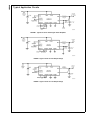
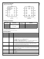
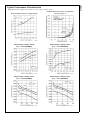
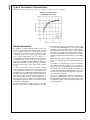
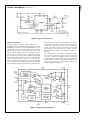
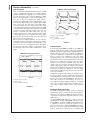
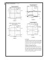
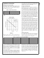
LM2614
400mA Sub-Miniature Adjustable DC-DC Converter
Optimized for RF Power Amplifiers
General Description
Key Specifications
The LM2614 DC-DC converter is optimized for powering RF
power amplifiers (PAs) from a single Lithium-Ion cell. It steps
down an input voltage of 2.8V to 5.5V to an output of 1.0V to
3.6V at up to 400mA (300mA for B grade). Output voltage is
set using an analog input to VCON in the application circuit.
The device offers three modes for mobile phones and similar
RF PA applications. Fixed-frequency PWM mode minimizes
RF interference. A SYNC input allows synchronizing the
switching frequency in a range of 500kHz to 1MHz. Low
current hysteretic PFM mode reduces quiescent current to
160µA (typ.). Shutdown mode turns the device off and reduces battery consumption to 0.02µA (typ.).
Current limit and thermal shutdown features protect the device and system during fault conditions.
The LM2614 is available in a 10 bump micro SMD package.
This packaging uses National’s chip-scale micro SMD technology and offers the smallest possible size. A high switching
frequency (600kHz) allows use of tiny surface-mount components.
The LM2614 can be dynamically controlled for output voltage changes from 1.0V to 3.6V in < 30µs. The device features external compensation to tailor the response to a wide
range of operating conditions.
Operates from a single LiION cell (2.8V to 5.5V)
Adjustable output voltage (1.0V to 3.6V)
± 1% DC feedback voltage precision
400mA maximum load capability(300mA for B grade)
600µA typ PWM mode quiescent current
0.02µA typ shutdown current
600kHz PWM switching frequency
SYNC input for PWM mode frequency synchronization
from 500kHz to 1MHz
n High efficiency (96% typ at 3.9VIN, 3.6VOUT and 200mA)
in PWM mode from internal synchronous rectification
n 100% Maximum Duty Cycle for Lowest Dropout
n
n
n
n
n
n
n
n
Features
n
n
n
n
n
n
n
Sub-miniature 10-bump thin micro SMD package
Uses small ceramic capacitors
5mV typ PWM mode output voltage ripple(COUT = 22µF)
Internal soft start
Current overload protection
Thermal Shutdown
External compensation
Applications
n
n
n
n
© 2002 National Semiconductor Corporation
DS200367
Mobile Phones
Hand-Held Radios
RF PC Cards
Battery Powered RF Devices
www.national.com
LM2614 400mA Sub-Miniature Adjustable DC-DC Converter Optimized for RF Power Amplifiers
August 2002
LM2614
Typical Application Circuits
20036701
FIGURE 1. Typical Circuit for Powering RF Power Amplifiers
20036702
FIGURE 2. Typical Circuit for 2.5V Output Voltage
20036703
FIGURE 3. Typical Circuit for 1.5V Output Voltage
www.national.com
2
LM2614
Connection Diagrams
10-Bump micro SMD Package
20036704
20036705
Top View
Bottom View
Ordering Information
Order Number
Package Type
NSC Package
Marking (*)
LM2614ATL
LM2614BTL
LM2614ATLX
10-bump Wafer Level Chip Scale
(micro SMD)
LM2614BTLX
Supplied As
XYTT S50A
250 Tape and Reel
XYTT S50B
250 Tape and Reel
XYTT S50A
3000 Tape and Reel
XYTT S50B
3000 Tape and Reel
(*) XY - denotes the date code marking (2 digit) in production
(*) TT - refers to die run/lot traceability for production
(*) S - product line designator
Package markings may change over the course of production.
Pin Description
Pin Number
Pin Name
A1
FB
Function
B1
EANEG
Inverting input of error amplifier
C1
EAOUT
Output of error amplifier
D1
SYNC/MODE
D2
EN
D3
PGND
C3
SW
B3
PVIN
Power Supply Voltage Input to the internal PFET switch. Connect to the input filter
capacitor.
A3
VDD
Analog Supply Input. If board layout is not optimum, an optional 0.1µF ceramic capacitor
is suggested.
A2
SGND
Feedback Analog Input.
Synchronization Input. Use this digital input for frequency selection or modulation control.
Set:
SYNC/MODE = high for low-noise 600kHz PWM mode
SYNC/MODE = low for low-current PFM mode
SYNC/MODE = a 500kHz–1MHz external clock for synchronization in PWM mode. (See
Synchronization and Operating Modes in the Device Information section.)
Enable Input. Set this Schmitt trigger digital input high for normal operation. For shutdown,
set low. Set EN low during system power-up and other low supply voltage conditions.
(See Shutdown Mode in the Device Information section.)
Power Ground
Switching Node connection to the internal PFET switch and NFET synchronous rectifier.
Connect to an inductor with a saturation current rating that exceeds the max Switch Peak
Current Limit of the LM2614.
Analog and Control Ground
3
www.national.com
LM2614
Absolute Maximum Ratings
(Note 1)
Storage Temperature Range
Lead Temperature
(Soldering, 10 sec.)
If Military/Aerospace specified devices are required,
please contact the National Semiconductor Sales Office/
Distributors for availability and specifications.
PVIN, VDD to SGND
EN, EAOUT, EANEG, SYNC/MODE
to SGND
FB, SW
260˚C
Junction Temperature (Note 2)
−0.2V to +6V
PGND to SGND, PVIN to VDD
−45˚C to +150˚C
−25˚C to +125˚C
± 2 kV
Minimum ESD Rating
−0.2V to +0.2V
(Human Body Model, C = 100 pF, R = 1.5 kΩ)
Thermal Resistance (θJA) (Note 3)
140˚C/W
−0.2V to +6V
(GND −0.2V) to
(VDD +0.2V)
Electrical Characteristics
Specifications with standard typeface are for TA = TJ = 25˚C, and those in boldface type apply over the full Operating Temperature Range of TA = TJ = −25˚C to +85˚C. Unless otherwise specified, PVIN = VDD = EN = SYNC/MODE = 3.6V.
Symbol
Parameter
Conditions
Min
Typ
Max
Units
VIN
Input Voltage Range
VFB
Feedback Voltage
VHYST
PFM Comparator Hysteresis
Voltage
PFM Mode (SYNC/MODE =
0V) (Note 5)
ISHDN
Shutdown Supply Current
VIN = 3.6V, EN = 0V
0.02
3
µA
IQ1_PWM
DC Bias Current into VDD
SYNC/MODE = VIN
FB = 2V
600
725
µA
SYNC/MODE = 0V
FB = 2V
160
195
µA
IQ2_PFM
PVIN = VDD = VIN (Note 4)
2.8
3.6
5.5
V
1.485
1.50
1.515
V
24
mV
RDSON (P)
Pin-Pin Resistance for
P FET
395
550
mΩ
RDSON (N)
Pin-Pin Resistance for
N FET
330
500
mΩ
RDSON (TC)
FET Resistance
Temperature Coefficient
0.5
ILIM
Switch Peak Current Limit
(Note 6)
VIH
Logic High Input, EN,
SYNC/MODE
VIL
Logic Low Input, EN,
SYNC/MODE
FSYNC
SYNC/MODE Clock
Frequency Range
FOSC
Internal Oscillator
Frequency
Tmin
%/C
LM2614ATL
510
690
850
LM2614BTL
400
690
980
0.95
1.3
0.4
(Note 7)
0.80
500
1000
LM2614ATL, PWM Mode
468
600
732
450
600
750
200
V
V
LM2614BTL, PWM Mode
Minimum ON-Time of PFET
Switch in PWM Mode
mA
kHz
kHz
ns
Note 1: Absolute Maximum Ratings indicate limits beyond which damage to the device may occur. Operating Ratings indicate conditions for which the device is
functional, but device specifications may not be guaranteed. For guaranteed specifications and associated test conditions, see the Min and Max limits and Conditions
in the Electrical Characteristics table. Typical (typ) specifications are mean or average values at 25˚C and are not guaranteed.
Note 2: Thermal shutdown will occur if the junction temperature exceeds 150˚C.
Note 3: Thermal resistance specified with 2 layer PCB (0.5/0.5 oz. cu).
Note 4: The LM2614 is designed for mobile phone applications where turn-on after system power-up is controlled by the system controller. Thus, it should be kept
in shutdown by holding the EN pin low until the input voltage exceeds 2.8V.
Note 5: The hysteresis voltage is the minimum voltage swing on the FB pin that causes the internal feedback and control circuitry to turn the internal PFET switch
on and then off during PFM mode. When resistor dividers are used like in the operating circuit of Figure 4, the hysteresis at the output will be the value of the
hysteresis at the feedback pin times the resistor divider ratio. In this case, 24mV (typ) x ((46.4k + 33.2k)/33.2k).
Note 6: Current limit is built-in, fixed, and not adjustable. If the current limit is reached while the voltage at the FB pin is pulled below 0.7V, the internal PFET switch
turns off for 2.5µs to allow the inductor current to diminish.
Note 7: SYNC driven with an external clock switching between VIN and GND. When an external clock is present at SYNC; the IC is forced to be in PWM mode at
the external clock frequency. The LM2614 synchronizes to the rising edge of the external clock.
www.national.com
4
LM2614
Typical Performance Characteristics
LM2614ATL, Circuit of Figure 4, VIN = 3.6V, TA = 25˚C, unless otherwise noted.
Shutdown Quiescent Current vs Temperature
(Circuit in Figure 3)
Quiescent Supply Current vs Supply Voltage
20036708
20036722
Output Voltage vs Supply Voltage
(VOUT = 1.5V, PWM MODE)
Output Voltage vs Supply Voltage
(VOUT = 1.0V, PWM MODE)
20036724
20036709
Output Voltage vs Output Current
(VOUT = 1.5V, PWM MODE)
Output Voltage vs Output Current
(VOUT = 1.0V, PWM MODE)
20036710
20036711
5
www.national.com
LM2614
Typical Performance Characteristics
LM2614ATL, Circuit of Figure 4, VIN = 3.6V, TA = 25˚C, unless otherwise noted. (Continued)
Output Voltage vs Output Current
(VOUT = 3.6V, PWM MODE)
Dropout Voltage vs Output Current
(VOUT = 3.6V, PWM MODE)
20036732
20036712
Switching Frequency vs Temperature
(Circuit in Figure 3, PWM MODE)
Feedback Bias Current vs Temperature
(Circuit in Figure 3)
20036723
20036731
Efficiency vs Output Current
(VOUT = 1.0V, PWM MODE, with Diode)
Efficiency vs Output Current
(VOUT = 1.0V, PWM MODE)
20036713
www.national.com
20036714
6
LM2614
Typical Performance Characteristics
LM2614ATL, Circuit of Figure 4, VIN = 3.6V, TA = 25˚C, unless otherwise noted. (Continued)
Efficiency vs Output Current
(VOUT = 1.5V, PWM MODE)
Efficiency vs Output Current
(VOUT = 1.5V, PWM MODE, with Diode)
20036715
20036716
Efficiency vs Output Current
(VOUT = 3.6V, PWM MODE, with Diode)
Efficiency vs Output Current
(VOUT = 3.6V, PWM MODE)
20036717
20036718
7
www.national.com
LM2614
Typical Performance Characteristics
LM2614ATL, Circuit of Figure 4, VIN = 3.6V, TA = 25˚C, unless otherwise noted. (Continued)
Efficiency vs Output Voltage
(PWM MODE, with Diode)
20036730
3.9V input. The efficiency can be further increased by using
a schottky diode like MBRM120 as shown in Figure 4. PWM
mode quiescent current is 600µA typ. The output voltage is
dynamically programmable from 1.0V to 3.6V by adjusting
the voltage on the VCON at the external feedback resistors.
This ensures longer battery life by being able to change the
PA supply voltage dynamically depending on its transmitting
power.
Additional features include soft-start, current overload protection, over voltage protection and thermal shutdown protection.
The LM2614 is constructed using a chip-scale 10-pin thin
micro SMD package. This package offers the smallest possible size, for space-critical applications such as cell phones,
where board area is an important design consideration. Use
of a high switching frequency (600kHz) reduces the size of
external components. Board area required for implementation is only 0.58in2 (375mm2).
Use of a micro-SMD package requires special design considerations for implementation. (See Micro SMD Package
Assembly and Use in the Application Information section.) Its
fine bump-pitch requires careful board design and precision
assembly equipment.
Device Information
The LM2614 is a simple, step-down DC-DC converter optimized for powering RF power amplifiers (PAs) in mobile
phones, portable communicators, and similar battery powered RF devices. It is designed to allow the RF PA to operate
at maximum efficiency over a wide range of power levels
from a single LiION battery cell. It is based on a
current-mode buck architecture, with synchronous rectification in PWM mode for high efficiency. It is designed for a
maximum load capability of 400mA (300mA for B grade) in
PWM mode. Maximum load range may vary from this depending on input voltage, output voltage and the inductor
chosen.
The device has all three of the pin-selectable operating
modes required for powering RF PAs in mobile phones and
other sophisticated portable devices with complex power
management needs. Fixed-frequency PWM operation offers
full output current capability at high efficiency while minimizing interference with sensitive IF and data acquisition circuits. During standby operation, hysteretic PFM mode reduces quiescent current to 160µA typ. to maximize battery
life. Shutdown mode turns the device off and reduces battery
consumption to 0.02µA (typ).
DC PWM mode feedback voltage precision is ± 1%. Efficiency is typically 96% for a 200mA load with 3.6V output,
www.national.com
8
LM2614
Device Information
(Continued)
20036706
FIGURE 4. Typical Operating Circuit
transferred back into the circuit and depleted, the inductor
current ramps down with a slope of VOUT/L. If the inductor
current reaches zero before the next cycle, the synchronous
rectifier is turned off to prevent current reversal. The output
filter capacitor stores charge when the inductor current is
high, and releases it when low, smoothing the voltage across
the load.
The output voltage is regulated by modulating the PFET
switch on time to control the average current sent to the load.
The effect is identical to sending a duty-cycle modulated
rectangular wave formed by the switch and synchronous
rectifier at SW to a low-pass filter formed by the inductor and
output filter capacitor. The output voltage is equal to the
average voltage at the SW pin.
CIRCUIT OPERATION
Referring to Figure 4, Figure 5, Figure 6 and Figure 7,
the LM2614 operates as follows. During the first part of each
switching cycle, the control block in the LM2614 turns on the
internal PFET switch. This allows current to flow from the
input through the inductor to the output filter capacitor and
load. The inductor limits the current to a ramp with a slope of
(VIN–VOUT)/L, by storing energy in a magnetic field. During
the second part of each cycle, the controller turns the PFET
switch off, blocking current flow from the input, and then
turns the NFET synchronous rectifier on. In response, the
inductor’s magnetic field collapses, generating a voltage that
forces current from ground through the synchronous rectifier
to the output filter capacitor and load. As the stored energy is
20036707
FIGURE 5. Simplified Functional Diagram
9
www.national.com
LM2614
Device Information
(Continued)
PFM Mode Switching Waveform
PWM OPERATION
While in PWM (Pulse Width Modulation) mode, the output
voltage is regulated by switching at a constant frequency
and then modulating the energy per cycle to control power to
the load. Energy per cycle is set by modulating the PFET
switch on-time pulse-width to control the peak inductor current. This is done by comparing the signal from the
current-sense amplifier with a slope compensated error signal from the voltage-feedback error amplifier. At the beginning of each cycle, the clock turns on the PFET switch,
causing the inductor current to ramp up. When the current
sense signal ramps past the error amplifier signal, the PWM
comparator turns off the PFET switch and turns on the NFET
synchronous rectifier, ending the first part of the cycle. If an
increase in load pulls the output voltage down, the error
amplifier output increases, which allows the inductor current
to ramp higher before the comparator turns off the PFET.
This increases the average current sent to the output and
adjusts for the increase in the load.
20036726
A: Inductor Current, 500mA/div
B: SW Pin, 2V/div
C: VOUT, 50mV/div, AC Coupled
Before going to the PWM comparator, the error signal is
summed with a slope compensation ramp from the oscillator
for stability of the current feedback loop. During the second
part of the cycle, a zero crossing detector turns off the NFET
synchronous rectifier if the inductor current ramps to zero.
The minimum on time of the PFET in PWM mode is about
200ns.
FIGURE 7.
PFM OPERATION
Connecting the SYNC/MODE to SGND sets the LM2614 to
hysteretic PFM operation. While in PFM (Pulse Frequency
Modulation) mode, the output voltage is regulated by switching with a discrete energy per cycle and then modulating the
cycle rate, or frequency, to control power to the load. This is
done by using an error comparator to sense the output
voltage. The device waits as the load discharges the output
filter capacitor, until the output voltage drops below the lower
threshold of the PFM error-comparator. Then the device
initiates a cycle by turning on the PFET switch. This allows
current to flow from the input, through the inductor to the
output, charging the output filter capacitor. The PFET is
turned off when the output voltage rises above the regulation
threshold of the PFM error comparator. Thus, the output
voltage ripple in PFM mode is proportional to the hysteresis
of the error comparator.
In PFM mode, the device only switches as needed to service
the load. This lowers current consumption by reducing power
consumed during the switching action in the circuit, due to
transition losses in the internal MOSFETs, gate drive currents, eddy current losses in the inductor, etc. It also improves light-load voltage regulation. During the second half
of the cycle, the intrinsic body diode of the NFET synchronous rectifier conducts until the inductor current ramps to
zero.
PWM Mode Switching Waveform
20036725
A: Inductor Current, 500mA/div
B: SW Pin, 2V/div
C: VOUT, 10mV/div, AC Coupled
FIGURE 6.
OPERATING MODE SELECTION
The LM2614 is designed for digital control of the operating
modes by the system controller. This prevents the spurious
switch over from low-noise PWM mode between transmission intervals in mobile phone applications that can occur in
other products.
The SYNC/MODE digital input pin is used to select the
operating mode. Setting SYNC/MODE high (above 1.3V)
selects 600kHz current-mode PWM operation. PWM mode
is optimized for low-noise, high-power operation for use
when the load is active. Setting SYNC/MODE low (below
0.4V) selects hysteretic voltage-mode PFM operation. PFM
mode is optimized for reducing power consumption and
www.national.com
10
EN should be set low to turn off the LM2614 during system
power-up and undervoltage conditions when the supply is
less than the 2.8V minimum operating voltage. The LM2614
is designed for compact portable applications, such as mobile phones. In such applications, the system controller determines power supply sequencing. Although the LM2614 is
typically well behaved at low input voltages, this is not guaranteed.
(Continued)
extending battery life when the load is in a low-power
standby mode. In PFM mode, quiescent current into the VDD
pin is 160µA typ. In contrast, PWM mode VDD-pin quiescent
current is 600µA typ.
PWM operation is intended for use with loads of 50mA or
more, when low noise operation is desired. Below 100mA,
PFM operation can be used to allow precise regulation, and
reduced current consumption. However, it should be noted
that for PA applications the PFM mode need not be used as
output voltage slew rates are of more concern to the system
designer. The LM2614 has an over-voltage feature that prevents the output voltage from rising too high, when the
device is left in PWM mode under low-load conditions. See
Overvoltage Protection, for more information.
Switch modes with the SYNC/MODE pin, using a signal with
a slew rate faster than 5V/100µs. Use a comparator, Schmitt
trigger or logic gate to drive the SYNC/MODE pin. Do not
leave the pin floating or allow it to linger between thresholds.
These measures will prevent output voltage errors in response to an indeterminate logic state. The LM2614
switches on each rising edge of SYNC. Ensure a minimum
load to keep the output voltage in regulation when switching
modes frequently.
INTERNAL SYNCHRONOUS RECTIFICATION
While in PWM mode, the LM2614 uses an internal NFET as
a synchronous rectifier to reduce rectifier forward voltage
drop and associated power loss. Synchronous rectification
provides a significant improvement in efficiency whenever
the output voltage is relatively low compared to the voltage
drop across an ordinary rectifier diode.
The internal NFET synchronous rectifier is turned on during
the inductor current down slope during the second part of
each cycle. The synchronous rectifier is turned off prior to the
next cycle, or when the inductor current ramps to zero at light
loads. The NFET is designed to conduct through its intrinsic
body diode during transient intervals before it turns on, eliminating the need for an external diode.
CURRENT LIMITING
A current limit feature allows the LM2614 to protect itself and
external components during overload conditions. In PWM
mode cycle-by-cycle current limit is normally used. If an
excessive load pulls the voltage at the feedback pin down to
approximately 0.7V, then the device switches to a timed
current limit mode. In timed current limit mode the internal
P-FET switch is turned off after the current comparator trips
and the beginning of the next cycle is inhibited for 2.5µs to
force the instantaneous inductor current to ramp down to a
safe value. Timed current limit mode prevents the loss of
current control seen in some products when the voltage at
the feedback pin is pulled low in serious overload conditions.
FREQUENCY SYNCHRONIZATION
The SYNC/MODE input can also be used for frequency
synchronization. During synchronization, the LM2614 initiates cycles on the rising edge of the clock. When synchronized to an external clock, it operates in PWM mode. The
device can synchronize to a 50% duty-cycle clock over
frequencies from 500kHz to 1MHz. If a different duty cycle is
used other than 50% the range for acceptable duty cycles
are 30% to 70%.
Use the following waveform and duty cycle guidelines when
applying an external clock to the SYNC/MODE pin. Clock
under/overshoot should be less than 100mV below GND or
above VDD. When applying noisy clock signals, especially
sharp edged signals from a long cable during evaluation,
terminate the cable at its characteristic impedance and add
an RC filter to the SYNC pin, if necessary, to soften the slew
rate and over/undershoot. Note that sharp edged signals
from a pulse or function generator can develop
under/overshoot as high as 10V at the end of an improperly
terminated cable.
DYNAMICALLY ADJUSTABLE OUTPUT VOLTAGE
The LM2614 can be used to provide dynamically adjustable
output voltage by using external feedback resistors. The
output can be varied from 1.0V to 3.6V in less than 30µs by
using an analog control signal (VCON) at the external feedback resistors. This feature is useful in PA applications
where peak power is needed only when the handset is far
away from the base station or when data is being transmitted. In other instances the transmitting power can be reduced and hence the supply voltage to the PA can be
reduced helping maintain longer battery life. See Setting the
Output Voltage in the Application Information section for
further details.
In dropout conditions the output voltage is VIN − IOUT (Rdc +
RDSON (P)) where Rdc is the series resistance of the inductor
and RDSON (P) is the on resistance of the PFET.
OVERVOLTAGE PROTECTION
The LM2614 has an over-voltage comparator that prevents
the output voltage from rising too high when the device is left
in PWM mode under low-load conditions. When the output
voltage rises by about 100mV (Figure 3) over its regulation
threshold, the OVP comparator inhibits PWM operation to
skip pulses until the output voltage returns to the regulation
threshold. When resistor dividers are used the OVP threshold at the output will be the value of the threshold at the
feedback pin times the resistor divider ratio. In over voltage
protection, output voltage and ripple will increase.
SHUTDOWN MODE
Setting the EN digital input pin low ( < 0.4V) places the
LM2614 in a 0.02µA (typ) shutdown mode. During shutdown,
the PFET switch, NFET synchronous rectifier, reference,
control and bias circuitry of the LM2614 are turned off.
Setting EN high enables normal operation. While turning on,
soft start is activated.
11
www.national.com
LM2614
Device Information
LM2614
Device Information
(Continued)
Load Transient Response
(Circuit in Figure 3)
VCON Transient Response
(Circuit in Figure 4)
20036727
20036719
FIGURE 10.
FIGURE 8.
Line Transient Response
(Circuit in Figure 3)
VCON Transient Response in Dropout
(Circuit in Figure 4)
20036728
20036720
FIGURE 11.
FIGURE 9.
SOFT-START
The LM2614 has soft start to reduce current inrush during
power-up and startup. This reduces stress on the LM2614
and external components. It also reduces startup transients
on the power source. Soft start is implemented by ramping
up the reference input to the error amplifier of the LM2614 to
gradually increase the output voltage.
THERMAL SHUTDOWN PROTECTION
The LM2614 has a thermal shutdown protection function to
protect itself from short-term misuse and overload conditions. When the junction temperature exceeds 150˚C the
device turns off the output stage and when the temperature
drops below 130˚C it initiates a soft start cycle. Prolonged
operation in thermal shutdown conditions may damage the
device and is considered bad practice.
www.national.com
12
SETTING THE OUTPUT VOLTAGE
The LM2614 can be used with external feedback resistors
and an analog signal to vary the output voltage. Select an
output voltage from 1.0V to 3.6V by setting the voltage on
the VCON as directed in Table 1.
EXTERNAL COMPENSATION
The LM2614 uses external components connected to the
EANEG and EAOUT pins to compensate the regulator (Figure 4). Typically, all that is required is a series connection of
one capacitor (C4) and one resistor (R3). A capacitor (C5)
can be connected across the EANEG and EAOUT pins to
improve the noise immunity of the loop. C5 reacts with R3 to
give a high frequency pole. C4 reacts with the high open loop
gain of the error amplifier and the resistance at the EANEG
pin to create the dominant pole for the system, while R3 and
C4 react to create a zero in the frequency response. The
pole rolls off the loop gain, to give a bandwidth somewhere
between 10kHz and 50kHz, this avoids a 100kHz parasitic
pole contributed by the current mode controller. Typical values in the 220pF to 1nF (C4) range are recommended to
create a pole on the order of 10Hz or less.
TABLE 1. Output Voltage Selection
VCON (V)
VOUT (V)
VCON = 0V
VFB (1+R1/R2)
VCON > 0V
VFB (1+R1/R2)−VCON (R1/R2)
Refer to Figure 12 for the relation between VOUT and
VCON.
VOUT vs VCON
(Circuit in Figure 4)
The next dominant pole in the system is formed by the output
capacitance (C2) and the parallel combination of the load
resistance and the effective output resistance of the regulator. This combined resistance (Ro) is dominated by the small
signal output resistance, which is typically in the range of 3Ω
to 15Ω. The exact value of this resistance, and therefore this
load pole depends on the steady state duty cycle and the
internal ramp value. Ideally we want the zero formed by R3
and C4 to cancel this load pole, such that R3=RoC2/C4. Due
to the large variation in Ro, this ideal case can only be
achieved at one operating condition. Therefore a compromise of about 5Ω for Ro should be used to determine a
starting value for R3. This value can then be optimized on
the bench to give the best transient response to load
changes and changes in VCON, under all conditions. Typical
values are 10pF for C5 and 220pF to 470pF for C4, to
ensure good response from dropout conditions to VOUT(min).
20036721
INDUCTOR SELECTION
Use a 10µH inductor with saturation current rating higher
than the peak current rating of the device. The inductor’s
resistance should be less than 0.3Ω for good efficiency.
Table 2 lists suggested inductors and suppliers.
FIGURE 12.
When the control voltage is between 1.85V and 0V, the
output voltage will vary in a monotonic fashion with respect
TABLE 2. Suggested Inductors and Their Suppliers
Part Number
Vendor
Phone
FAX
847-639-1469
DO1608C-103
Coilcraft
847-639-6400
P1174.103T
Pulse
858-674-8100
858-674-8262
ELL6RH100M
Panasonic
714-373-7366
714-373-7323
CDRH5D18-100
Sumida
847-956-0666
847-956-0702
P0770.103T
Pulse
858-674-8100
858-674-8262
For low-cost applications, an unshielded inductor is suggested. For noise critical applications, a toroidal or shielded
inductor should be used. A good practice is to lay out the
board with footprints accommodating both types for design
flexibility. This allows substitution of a low-noise shielded
inductor, in the event that noise from low-cost unshielded
models is unacceptable.
The saturation current rating is the current level beyond
which an inductor loses its inductance. Different manufacturers specify the saturation current rating differently. Some
specify saturation current point to be when inductor value
falls 30% from its original value, others specify 10%. It is
always better to look at the inductance versus current curve
and make sure the inductor value doesn’t fall below 30% at
the peak current rating of the LM2614. Beyond this rating,
the inductor loses its ability to limit current through the PWM
switch to a ramp. This can cause poor efficiency, regulation
errors or stress to DC-DC converters like the LM2614. Saturation occurs when the magnetic flux density from current
through the windings of the inductor exceeds what the inductor’s core material can support with a corresponding
magnetic field.
13
www.national.com
LM2614
to the voltage on the control pin as per the equation in Table
1. Select the value of R2 to allow at least 100 times the
feedback pin bias current to flow through it.
Application Information
LM2614
Application Information
and/or increased tolerance to heavy load transients. A 10µF
ceramic output capacitor can be used in applications where
the worst case load transient step is less than 200mA. Table
3 lists suggested capacitors and suppliers.
The input filter capacitor supplies current to the PFET switch
of the LM2614 in the first part of each cycle and reduces
voltage ripple imposed on the input power source. The output filter capacitor smoothes out current flow from the inductor to the load, helps maintain a steady output voltage during
transient load changes and reduces output voltage ripple.
These capacitors must be selected with sufficient capacitance and sufficiently low ESR to perform these functions.
Parallel combinations of smaller value ceramic capacitors
can also be used on the output as long as the combined
value is at least 4.7µF for the application circuit in Figure 1.
The ESR, or equivalent series resistance, of the filter capacitors is a major factor in voltage ripple.
(Continued)
CAPACITOR SELECTION
Use a 4.7µF or 10µF ceramic input capacitor. A 10µF ceramic input capacitor is recommended if the PA represents a
load < 14Ω. Use a 4.7µF ceramic output capacitor for getting
faster slew rates for output voltages from VOUT (min) to VOUT
(max). Use X7R or X5R types, do not use Y5V. The rise
time for the voltage from VOUT (min) to VOUT (max) depends
on the slew rate of the error amp, switch peak current limit
and the value of the output capacitor. The time for the output
to change from VOUT (max) to VOUT (min) depends on RLOAD
and COUT. Use of tantalum capacitors is not recommended.
Ceramic capacitors provide an optimal balance between
small size, cost, reliability and performance for cell phones
and similar applications. A 22µF ceramic output capacitor
can be used in applications requiring fixed output voltages
TABLE 3. Suggested Capacitors and Their Suppliers
Model
Type
Vendor
Phone
FAX
C1, C2 (Input or Output Filter Capacitor)
JMK212BJ475MG
Ceramic
Taiyo-Yuden
847-925-0888
847-925-0899
LMK316BJ475ML
Ceramic
Taiyo-Yuden
847-925-0888
847-925-0899
C2012X5R0J475K
Ceramic
TDK
847-803-6100
847-803-6296
JMK325BJ226MM
Ceramic
Taiyo-Yuden
847-925-0888
847-925-0899
JMK212BJ106MG
Ceramic
Taiyo-Yuden
847-925-0888
847-925-0899
micro SMD PACKAGE ASSEMBLY AND USE
Use of the micro SMD package requires specialized board
layout, precision mounting and careful reflow techniques, as
detailed in National Semiconductor Application Note
AN-1112. Refer to the section Surface Mount Technology
(SMT) Assembly Considerations. For best results in assembly, alignment ordinals on the PC board should be used to
facilitate placement of the device.
The pad style used with micro SMD package must be the
NSMD (non-solder mask defined) type. This means that the
solder-mask opening is larger than the pad size. This prevents a lip that otherwise forms if the solder-mask and pad
overlap, from holding the device off the surface of the board
and interfering with mounting. See Application Note AN-1112
for specific instructions how to do this.
The 10-Bump package used for the LM2614 has 300 micron
solder balls and requires 10.82mil pads for mounting on the
circuit board. The trace to each pad should enter the pad
with a 90˚ entry angle to prevent debris from being caught in
deep corners. Initially, the trace to each pad should be
6–7mil wide, for a section approximately 6mil long, as a
thermal relief. Then each trace should neck up or down to its
optimal width. The important criterion is symmetry. This ensures the solder bumps on the LM2614 reflow evenly and
that the device solders level to the board. In particular,
special attention must be paid to the pads for bumps D3–B3.
Because PGND and PVIN are typically connected to large
copper planes, inadequate thermal reliefs can result in late
or inadequate reflow of these bumps.
The micro SMD package is optimized for the smallest possible size in applications with red or infrared opaque cases.
Because the micro SMD package lacks the plastic encapsulation characteristic of larger devices, it is vulnerable to light.
Backside metalization and/or epoxy coating, along with
front-side shading by the printed circuit board, reduce this
sensitivity.
www.national.com
BOARD LAYOUT CONSIDERATIONS
PC board layout is an important part of DC-DC converter
design. Poor board layout can disrupt the performance of a
DC-DC converter and surrounding circuitry by contributing to
EMI, ground bounce, and resistive voltage loss in the traces.
These can send erroneous signals to the DC-DC converter
IC, resulting in poor regulation or instability. Poor layout can
also result in reflow problems leading to poor solder joints
between the micro SMD package and board pads. Poor
solder joints can result in erratic or degraded performance.
Good layout for the LM2614 can be implemented by following a few simple design rules.
1. Place the LM2614 on 10.82 mil (10.82/1000 in.) pads.
As a thermal relief, connect to each pad with a 7 mil
wide, approximately 7 mil long traces, and then incrementally increase each trace to its optimal width. The
important criterion is symmetry to ensure the solder
bumps on the LM2614 reflow evenly (see micro SMD
Package Assembly and Use).
2. Place the LM2614, inductor and filter capacitors close
together and make the traces short. The traces between
these components carry relatively high switching currents and act as antennas. Following this rule reduces
radiated noise. Place the capacitors and inductor within
0.2 in. (5 mm) of the LM2614.
14
reduces voltage errors caused by resistive losses across
the traces.
(Continued)
3. Arrange the components so that the switching current
loops curl in the same direction. During the first half of
each cycle, current flows from the input filter capacitor,
through the LM2614 and inductor to the output filter
capacitor and back through ground, forming a current
loop. In the second half of each cycle, current is pulled
up from ground, through the LM2614 by the inductor, to
the output filter capacitor and then back through ground,
forming a second current loop. Routing these loops so
the current curls in the same direction prevents magnetic field reversal between the two half-cycles and reduces radiated noise.
4. Connect the ground pins of the LM2614, and filter capacitors together using generous component-side copper fill as a pseudo-ground plane. Then, connect this to
the ground-plane (if one is used) with several vias. This
reduces ground-plane noise by preventing the switching
currents from circulating through the ground plane. It
also reduces ground bounce at the LM2614 by giving it
a low-impedance ground connection.
6. Route noise sensitive traces, such as the voltage feedback path, away from noisy traces between the power
components. The voltage feedback trace must remain
close to the LM2614 circuit and should be routed directly
from VOUT at the output capacitor and should be routed
opposite to noise components. This reduces EMI radiated onto the DC-DC converter’s own voltage feedback
trace.
7. Place noise sensitive circuitry, such as radio IF blocks,
away from the DC-DC converter, CMOS digital blocks
and
other
noisy
circuitry.
Interference
with
noise-sensitive circuitry in the system can be reduced
through distance.
In mobile phones, for example, a common practice is to
place the DC-DC converter on one corner of the board,
arrange the CMOS digital circuitry around it (since this also
generates noise), and then place sensitive preamplifiers and
IF stages on the diagonally opposing corner. Often, the
sensitive circuitry is shielded with a metal pan and power to
it is post-regulated to reduce conducted noise, using
low-dropout linear regulators.
5. Use wide traces between the power components and for
power connections to the DC-DC converter circuit. This
15
www.national.com
LM2614
Application Information
LM2614 400mA Sub-Miniature Adjustable DC-DC Converter Optimized for RF Power Amplifiers
Physical Dimensions
inches (millimeters) unless otherwise noted
NOTES: UNLESS OTHERWISE SPECIFIED
1. EPOXY COATING
2. 63Sn/37Pb EUTECTIC BUMP
3. RECOMMEND NON-SOLDER MASK DEFINED LANDING PAD.
4. PIN A1 IS ESTABLISHED BY LOWER LEFT CORNER WITH RESPECT TO TEXT ORIENTATION.
5. XXX IN DRAWING NUMBER REPRESENTS PACKAGE SIZE VARIATION WHERE X1 IS PACKAGE WIDTH, X2 IS PACKAGE LENGTH AND X3 IS
PACKAGE HEIGHT.
6. REFERENCE JEDEC REGISTRATION MO-211. VARIATION BD.
10-Bump micro SMD Package
NS Package Number TLP106WA
The dimensions for X1, X2 and X3 are as given:
X1 = 2.250 ± 0.030 mm
X2 = 2.504 ± 0.030 mm
X3 = 0.600 ± 0.075 mm
LIFE SUPPORT POLICY
NATIONAL’S PRODUCTS ARE NOT AUTHORIZED FOR USE AS CRITICAL COMPONENTS IN LIFE SUPPORT
DEVICES OR SYSTEMS WITHOUT THE EXPRESS WRITTEN APPROVAL OF THE PRESIDENT AND GENERAL
COUNSEL OF NATIONAL SEMICONDUCTOR CORPORATION. As used herein:
1. Life support devices or systems are devices or
systems which, (a) are intended for surgical implant
into the body, or (b) support or sustain life, and
whose failure to perform when properly used in
accordance with instructions for use provided in the
labeling, can be reasonably expected to result in a
significant injury to the user.
National Semiconductor
Corporation
Americas
Email: [email protected]
www.national.com
National Semiconductor
Europe
Fax: +49 (0) 180-530 85 86
Email: [email protected]
Deutsch Tel: +49 (0) 69 9508 6208
English Tel: +44 (0) 870 24 0 2171
Français Tel: +33 (0) 1 41 91 8790
2. A critical component is any component of a life
support device or system whose failure to perform
can be reasonably expected to cause the failure of
the life support device or system, or to affect its
safety or effectiveness.
National Semiconductor
Asia Pacific Customer
Response Group
Tel: 65-2544466
Fax: 65-2504466
Email: [email protected]
National Semiconductor
Japan Ltd.
Tel: 81-3-5639-7560
Fax: 81-3-5639-7507
National does not assume any responsibility for use of any circuitry described, no circuit patent licenses are implied and National reserves the right at any time without notice to change said circuitry and specifications.