1
PCF50633
NXP Semiconductors
PCF50633 User Manual
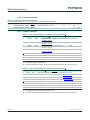
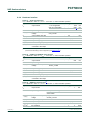
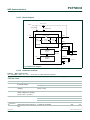
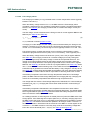
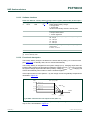
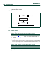
8.11.5 Software interface
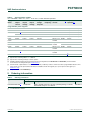
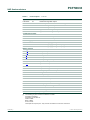
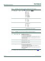
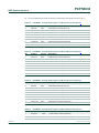
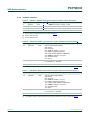
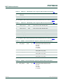
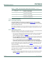
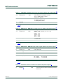
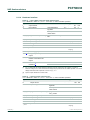
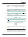
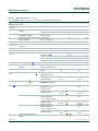
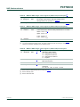
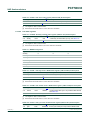
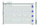
Table 76.
LDO1OUT - LDO1 output voltage select register (address 2Dh) bit description[1]
Bit
Symbol
Access
Description
4:0
ldo1_out
R/W
VO(prog) = 0.9 + ldo1_out × 0.1 V (max 3.6V); e.g.
00000
00001
11000
11011
11111
5
ldo1_swmod
7:6
reserved
[1]
R/W
: 0.9 V
: 1.0 V
: 3.3 V
: 3.6 V
: 3.6 V
0: linear regulator mode
1: switch mode
This register is reset at each transition to Standby state. Reset values are determined by the IC variant (see
Table 7).
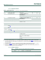
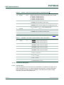
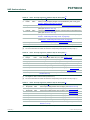
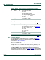
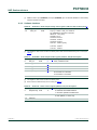
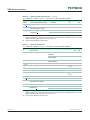
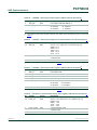
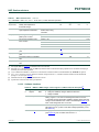
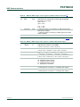
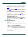
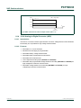
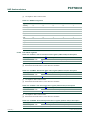
Table 77.
LDO1ENA - LDO1 output enable register (address 2Eh) bit description[1]
Bit
Symbol
Access
Description
0
ldo1_on
R/W
if set, LDO is ON
1
ldo1_p1c
R/W
if set, LDO is ON when GPIO1 = 1
2
ldo1_p2c
R/W
if set, LDO is ON when GPIO2 = 1
3
ldo1_p3c
R/W
if set, LDO is ON when GPIO3 = 1
5:4
ldo1_ena_act
R/W
selects activation phase:
00: ACTPH1
01: ACTPH2
10: ACTPH3
11: ACTPH4
7:6
reserved
[1]
This register is reset at each transition to Standby state. Reset values are determined by the IC variant (see
Table 7).
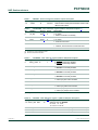
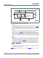
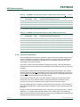
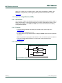
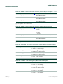
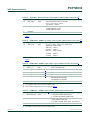
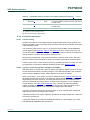
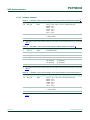
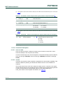
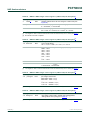
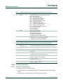
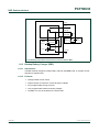
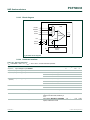
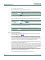
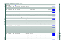
Table 78.
LDO2OUT - LDO2 output voltage select register (address 2Fh) bit description[1]
Bit
Symbol
Access
Description
4:0
ldo2_out
R/W
VO(prog) = 0.9 + ldo2_out × 0.1V (max 3.6 V); eg.
00000 : 0.9 V
00001 : 1.0 V
11000 : 3.3 V
11011 : 3.6 V
11111 : 3.6 V
5
ldo2_swmod
7:6
reserved
[1]
R/W
0: linear regulator mode
1: switch mode
This register is reset at each transition to Standby state. Reset values are determined by the IC variant (see
Table 7).
PCF50633UM_6
User manual
© NXP B.V. 2008. All rights reserved.
Rev. 06 — 05 March 2008
69 of 125