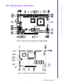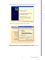
1
User Manual
PCI-6873
AMD GeodeTM LX800 PCI
Half-size SBC with VGA/LCD/
LVDS/LAN/SATA and SSD
Copyright
This document is copyrighted, © 2008. All rights are reserved. The original manufacturer reserves the right to make improvements to the products described in this manual at any time without notice.
No part of this manual may be reproduced, copied, translated or transmitted in any
form or by any means without the prior written permission of the original manufacturer. Information provided in this manual is intended to be accurate and reliable.
However, the original manufacturer assumes no responsibility for its use, nor for any
infringements upon the rights of third parties that may result from such use.
Acknowledgements
Award is a trademark of Award Software International, Inc.
VIA is a trademark of VIA Technologies, Inc.
IBM, PC/AT, PS/2 and VGA are trademarks of International Business Machines Corporation.
Intel and Pentium are trademarks of Intel Corporation.
Microsoft Windows® is a registered trademark of Microsoft Corp.
RTL is a trademark of Realtek Semi-Conductor Co., Ltd.
ESS is a trademark of ESS Technology, Inc.
UMC is a trademark of United Microelectronics Corporation.
SMI is a trademark of Silicon Motion, Inc.
Creative is a trademark of Creative Technology LTD.
All other product names or trademarks are properties of their respective owners.
For more information on this and other Advantech products, please visit our websites
at:
http://www.advantech.com
http://www.advantech.com/eplatform
For technical support and service, please visit our support website at:
http://www.advantech.com/support
This manual is for the PCI-6873.
PCI-6873 User Manual
Part No. 2002687300
Edition 1
Printed in China
November 2008
ii
Packing List
Before you begin installing your card, please make sure that the following materials
have been shipped:
! 1 x PCI-6873 half-size SBC
! 1 x Startup manual
! 1 x Utility CD
! 1 FDD cable
p/n:1701340705
! 1 IDE HDD cable(40P 60cm)
p/n:1701400607
! 1 Y Cable for PS/2 Keyboard, PS/2 Mouse
p/n:1700060202
! 1 Serial SATA HDD data cable
p/n:1700003194
! 1 Serial SATA HDD power cable
p/n:1703150102
! 1 Printer (2.54 mm pitch) +
RS-232 (2.0 mm pitch) cable w/ bracket
p/n:1700008891
! 1 USB cable with 4 ports (2.0 mm pitch)
p/n:1700008887
! 1 ATX feature cable
p/n:1700002343
! 1 Power cable
p/n:1700000265
! 1 Jumper pack
p/n:9689000002
Optional accessories:
!
!
!
!
!
Parallel port cable
IDE HDD cable(80P)
COM2 (RS-232/422/485) cable (2.0 mm pitch)
COM3 & 4 (RS-232) cable with bracket
(2.0 mm pitch)
Audio module with Line-in, Line-out, Mic
p/n:1701260301
p/n:1701400452
p/n: 1701140201
p/n: 1700001166
p/n: PCM-231A-00A1E
If any of these items are missing or damaged, contact your distributor or sales representative immediately.
PCI-6873 comparison table
Model
Memory
onboard
SATA TTL
LVDS LAN
COM
USB
PCI-6873L-L0
256 MB
0
1
0
1 x 8100C
4
4
PCI-6873F-L0
256 MB
2
1
1
1 x 8100C
4
4
PCI-6873PZ2-L0
no
2
1
1
1 x 8100C
4
4
iii
PCI-6873 User Manual
PCI-6873 memory compatibility table
Brand
Apacer
Kingston
MT
Size Speed Type
ECC Vendor PN
Advantech
Memory
PN
128 DDR2 DDR
N
MB 66
SODIMM
77.10920.110
AM1 22561615A7A
256 DDR3 DDR
N
MB 33
SODIMM
77.10634.190
Infineon
HYB25D256807B
T-5
128 DDR2 DDR
N
MB 66
SODIMM
KVR266X64SC
25/128
hynix 216A
HY5DU281622AT
-H
128 DDR3 DDR
N
MB 33
SODIMM
KVR333X64SC
25/128
ELPIDA SINGAPORE
DD2516AKTA-6BE
256 DDR2 DDR
N
MB 66
SODIMM
hynix 417A
HY5DU561622CT
-H
256 DDR3 DDR
N
MB 33
SODIMM
hynix 346AA
HY5DU561622CT
-J
512 DDR2 DDR
N
MB 66
SODIMM
KVR266X64SC
25/512
hynix 336AA
HY5DU121622AT
-H
512 DDR3 DDR
N
MB 33
SODIMM
KVR333X64SC
25/512
Infineon
HYB25D256800B
C-6
128 DDR2 DDR
N
MB 66
SODIMM
PC2100S2533-0-C1
MT 46V16M16
TG-75B
128 DDR3 DDR
N
MB 33
SODIMM
96SDSamsung 734
TS1DSG11800128M333NN K4H561638H6S
-TR
UCCC(16 x 16)
128 DDR2 DDR
N
MB 66
SODIMM
Infineon
HYB25D128800A
T-7
256 DDR3 DDR
N
MB 33
SODIMM
96SDINFINEON
TS3DSM11800
256M333NN HYB25DC512160
-6I
-TR
CE-5C(32 x 16)
512 DDR2 DDR
N
MB 66
SODIMM
96SDSamsung 719
TS6DSJ12202512M266NN K4H510838D7S
-TR2
UCCC(32 x 8)
512 DDR3 DDR
N
MB 33
SODIMM
96SDhynix 716A
TS6DSM11800
512M333NN HY5DU22CTP-6Y
-TR
D43
Transcend
1GB
PCI-6873 User Manual
DDR3 DDR
N
33
SODIMM
96SDTS2DSA187021G333NN6S
TR
iv
Samsung 719
K4H510838DZCCC(64 x 8)
Additional Information and Assistance
1.
2.
Visit the Advantech website at www.advantech.com where you can find the latest information about the product.
Contact your distributor, sales representative, or Advantech's customer service
center for technical support if you need additional assistance. Please have the
following information ready before you call:
!
Product name and serial number
!
Description of your peripheral attachments
!
Description of your software (operating system, version, application software, etc.)
!
A complete description of the problem
!
The exact wording of any error messages
Declaration of Conformity
FCC
This device complies with the requirements in part 15 of the FCC rules: Operation is
subject to the following two conditions:
1. This device may not cause harmful interference, and
2. This device must accept any interference received, including interference that
may cause undesired operation
This equipment has been tested and found to comply with the limits for a Class A digital device, pursuant to Part 15 of the FCC Rules. These limits are designed to provide reasonable protection against harmful interference when the equipment is
operated in a commercial environment. This equipment generates, uses, and can
radiate radio frequency energy and, if not installed and used in accordance with the
instruction manual, may cause harmful interference to radio communications. Operation of this device in a residential area is likely to cause harmful interference in which
case the user will be required to correct the interference at his/her own expense. The
user is advised that any equipment changes or modifications not expressly approved
by the party responsible for compliance would void the compliance to FCC regulations and therefore, the user's authority to operate the equipment.
Caution! There is a danger of a new battery exploding if it is incorrectly installed.
Do not attempt to recharge, force open, or heat the battery. Replace the
battery only with the same or equivalent type recommended by the manufacturer. Discard used batteries according to the manufacturer’s
instructions.
v
PCI-6873 User Manual
PCI-6873 User Manual
vi
Contents
Chapter
1
General Information ............................1
1.1
1.2
1.3
Introduction ............................................................................................... 2
Features .................................................................................................... 2
Specifications ............................................................................................ 3
1.3.1 PCI Half-size SBC Functions ........................................................ 3
1.3.2 VGA/LVDS Interface ..................................................................... 4
1.3.3 Ethernet Interface ......................................................................... 4
1.3.4 OS Support ................................................................................... 4
1.3.5 Mechanical and Environmental..................................................... 4
Board layout: dimensions.......................................................................... 5
Figure 1.1 Board Layout: Dimensions (Component Side) ........... 5
Figure 1.2 Board Layout: Dimensions (Solder Side) ................... 5
1.4
Chapter
2
Installation............................................7
2.1
Jumpers .................................................................................................... 8
Table 2.1: Jumpers...................................................................... 8
2.1.1 Clear CMOS (CN8) ....................................................................... 8
Table 2.2: Clear CMOS (CN8)..................................................... 8
2.1.2 LVDS Power select (CN14) .......................................................... 8
Table 2.3: LVDS Power select (CN14) ........................................ 8
2.1.3 COM2 Setting (CN19)................................................................... 9
Table 2.4: COM2 Setting (CN19) ................................................ 9
2.1.4 AT/ATX Selector (CN34)............................................................... 9
Table 2.5: AT/ATX Selector (CN34) ............................................ 9
Connectors.............................................................................................. 10
Table 2.6: Connectors ............................................................... 10
Locating Connectors ............................................................................... 11
Figure 2.1 Jumper & Connector Locations (component side) ... 11
Figure 2.2 Jumper & Connector Locations (solder side) ........... 11
Setting Jumpers ...................................................................................... 12
Installing SO-DIMM ................................................................................. 13
IDE, CDROM hard drive connector (CN4) .............................................. 14
2.6.1 Connecting the hard drive........................................................... 14
Solid State Disk....................................................................................... 14
2.7.1 CompactFlash (CN33) ................................................................ 14
Parallel port connector (CN2).................................................................. 14
Keyboard and PS/2 mouse connector (CN29)........................................ 14
Front Panel (CN1) ................................................................................... 15
2.10.1 HDD LED (Pin 1 & Pin 2) ............................................................ 15
2.10.2 POWER LED (Pin3 & Pin4) ........................................................ 15
2.10.3 Suspend led (PIN 5 & Pin 6) ....................................................... 15
2.10.4 Reset (Pin7&Pin8) ...................................................................... 15
2.10.5 Power Button (Pin9 & Pin10) ...................................................... 15
Power connectors ................................................................................... 15
2.11.1 Main power connector (CN15) .................................................... 15
2.11.2 ATX Feature connector (CN26) .................................................. 15
COM port connector (CN20, CN21, CN22)............................................. 16
2.12.1 Serial Port RS-422/485 (CN22, CN19) ....................................... 16
Table 2.7: Serial Port RS-422/485 (CN19) ................................ 16
VGA/LCD/LVDS interface connections ................................................... 16
2.13.1 CRT display connector (CN16) ................................................... 16
2.13.2 TTL TFT LCD connector (CN11) ................................................ 16
2.13.3 LVDS LCD panel connector (CN12) ........................................... 16
2.2
2.3
2.4
2.5
2.6
2.7
2.8
2.9
2.10
2.11
2.12
2.13
vii
PCI-6873 User Manual
2.15
2.16
2.17
2.18
2.19
2.20
2.21
2.22
2.23
2.13.4 LCD Inverter Connector (CN5) ................................................... 17
Ethernet configuration............................................................................. 17
2.14.1 100Base-T connector (CN18)..................................................... 17
2.14.2 Network boot (Depends on Ethernet Controller)......................... 17
Watchdog timer configuration ................................................................. 17
USB connectors (CN9, CN10) ................................................................ 17
GPIO (General Purpose Input Output) (CN17) ....................................... 17
Floppy Connector (CN2) ......................................................................... 17
SATA connector (CN6, CN7) .................................................................. 18
AC97 connector (CN23).......................................................................... 18
System FAN (CN24) ............................................................................... 18
External Keyboard Connector (CN28) .................................................... 18
PCI golden finger power (CN30)............................................................ 18
3
BIOS Operation ................................. 19
3.1
3.2
BIOS Introduction.................................................................................... 20
BIOS Setup ............................................................................................. 20
Table 3.1: Control Keys............................................................. 20
3.2.1 Main Menu .................................................................................. 21
3.2.2 Standard CMOS Features .......................................................... 22
3.2.3 Advanced BIOS Features ........................................................... 23
3.2.4 Advanced Chipset Features ....................................................... 25
3.2.5 Integrated Peripherals ................................................................ 27
3.2.6 Power Management Setup ......................................................... 29
3.2.7 PnP/PCI Configurations.............................................................. 30
3.2.8 PC Health Status ........................................................................ 31
3.2.9 Load Optimized Defaults ............................................................ 31
3.2.10 Set Password.............................................................................. 32
3.2.11 Save & Exit Setup....................................................................... 34
3.2.12 Quit Without Saving .................................................................... 34
2.14
Chapter
Chapter
4
4.1
4.4
Installation of chipset (AES) Driver ......................................................... 36
4.1.1 Windows XP driver setup............................................................ 36
PCI SVGA/LCD Introduction ................................................................... 39
4.2.1 Display type ................................................................................ 39
4.2.2 Dual Simultaneous Display......................................................... 39
4.2.3 CMOS setting for panel type....................................................... 39
4.2.4 Installation of VGA driver ............................................................ 39
SATA Introduction (Silicon Image Sil3512)............................................. 43
4.3.1 Update Sil 3512 driver on Windows XP (Non-RAID) .................. 43
4.3.2 Windows XP Fresh Installation (Non-RAID) ............................... 46
4.3.3 SATA RAID Mode Installation..................................................... 48
IDE Channel............................................................................................ 48
5
Audio Setup....................................... 53
5.1
5.2
Introduction ............................................................................................. 54
Driver installation .................................................................................... 54
5.2.1 Before you begin......................................................................... 54
5.2.2 Windows XP drivers.................................................................... 54
4.2
4.3
Chapter
Installation of Chipset, VGA and
SATA/IDE35
PCI-6873 User Manual
viii
Appendix A
Pin Assignments ...............................57
A.1
Front Panel (CN1) ................................................................................... 58
Table A.1: Front Panel (CN1) .................................................... 58
Printer Port Connector (CN2).................................................................. 58
Table A.2: Printer Port Connector (CN2) ................................... 58
Floppy Connector (CN3) ......................................................................... 59
Table A.3: Floppy Connector (CN3)........................................... 59
IDE Connector (CN4) .............................................................................. 60
Table A.4: IDE Connector (CN4) ............................................... 60
LCD Inverter Connector (CN5)................................................................ 60
Table A.5: LCD Inverter Connector (CN5) ................................. 60
SATA Connector (CN6,CN7) .................................................................. 60
Table A.6: SATA Connector (CN6, CN7)................................... 60
Clear CMOS (CN8) ................................................................................. 61
Table A.7: Clear CMOS (CN8)................................................... 61
USB connector (CN9,CN10) ................................................................... 61
Table A.8: USB connector (CN9, CN10).................................... 61
TFT LCD Connector (CN11) ................................................................... 61
Table A.9: TFT LCD Connector (CN11)..................................... 61
LVDS Connector (CN12)......................................................................... 62
Table A.10:LVDS Connector (CN12) .......................................... 62
LAN2 Connector (CN13) ......................................................................... 62
Table A.11:LAN2 Connector (CN13) .......................................... 62
LVDS Power select (CN14)..................................................................... 62
Table A.12:LVDS Power select (CN14) ...................................... 62
ATX Power connector (CN15)................................................................. 62
Table A.13:ATX Power connector (CN15) .................................. 62
VGA connector (CN16) ........................................................................... 63
Table A.14:VGA connector (CN16)............................................. 63
GPIO connector (CN17).......................................................................... 63
Table A.15:GPIO connector (CN17) ........................................... 63
LAN1 RJ45 connector (CN18) ................................................................ 63
Table A.16:LAN1 RJ45 connector (CN18).................................. 63
RS232/422/485 Select Jumper (CN19)................................................... 63
Table A.17:RS232/422/485 Select Jumper (CN19) .................... 63
COM3/COM4 Connector (CN20) ............................................................ 64
Table A.18:COM3/COM4 Connector (CN20).............................. 64
COM port1 (CN21) .................................................................................. 64
Table A.19:COM port1 RS232 (CN21) ....................................... 64
COM port2 (CN22) .................................................................................. 64
Table A.20:COM port2 RS232/422/485 (CN22) ......................... 64
AC97 Audio Connector (CN23)............................................................... 65
Table A.21:AC97 Audio Connector (CN23) ................................ 65
System FAN Connector (CN24).............................................................. 65
Table A.22:System FAN Connector (CN24) ............................... 65
Audio Connector (CN25)......................................................................... 65
Table A.23:Audio Connector (CN25) .......................................... 65
ATX Feature power connector (CN26).................................................... 65
Table A.24:ATX Feature power connector (CN26) ..................... 65
External Keyboard Connector (CN28) .................................................... 66
Table A.25:External Keyboard Connector (CN28)...................... 66
Keyboard/Mouse Connector (CN29)....................................................... 66
Table A.26:Keyboard/Mouse Connector (CN29) ........................ 66
PCI Golden finger Connector, -12 V (CN30)........................................... 66
Table A.27:PCI Golden finger Connector, -12 V (CN30) ............ 66
CD IN connector (CN32) ......................................................................... 66
Table A.28:CD IN connector (CN32) .......................................... 66
CF connector (CN33) .............................................................................. 66
AT/ATX Selector (CN34)......................................................................... 66
Table A.29:AT/ATX Selector (CN34) .......................................... 66
A.2
A.3
A.4
A.5
A.6
A.7
A.8
A.9
A.10
A.11
A.12
A.13
A.14
A.15
A.16
A.17
A.18
A.19
A.20
A.21
A.22
A.23
A.24
A.25
A.26
A.27
A.28
A.29
A.30
ix
PCI-6873 User Manual
Appendix B
System Assignments........................ 67
B.1
System I/O Ports..................................................................................... 68
Table B.1: System I/O ports....................................................... 68
1st MB memory map............................................................................... 68
Table B.2: 1st MB memory map ................................................ 68
DMA channel assignments ..................................................................... 69
Table B.3: DMA channel assignments....................................... 69
Interrupt Assignments ............................................................................. 69
Table B.4: Interrupt Assignments .............................................. 69
B.2
B.3
B.4
Appendix C
Mechanical Drawings ....................... 71
C.1
Mechanical Drawings.............................................................................. 72
Figure C.1 Dimensions of PCI-6873 (Component Side) ............ 72
Figure C.2 Dimensions of PCI-6873 (Solder Side) .................... 72
Appendix D
Watchdog Timer................................ 73
PCI-6873 User Manual
x
Chapter
1
1
General Information
This chapter gives background
information on the PCI-6873.
Sections include:
! Introduction
! Features
! Specifications
! Board layout and dimensions
1.1 Introduction
The PCI-6873 is a fanless, cost-effective, and reliable half-size SBC (Single board
computer) geared to satisfy the needs for various industrial computing equipment.
This product is ideal for the system manufacturers, integrators, or VARs that want to
provide performance, reliability, and quality at a reasonable price.
For those who want superior performance for various low-power embedded applications, PCI-6873 uses an AMD LX-800 processor clocked at 500 MHz, in conjunction
with flexible DDR333 system memory through one SODIMM socket supporting up to
1 GB, or through on-board DDR memory integrated up to 256 MB to achieve antivibration application. PCI-6873 also supports two SATA ports through PCI to SATA
bridge that allows the use of thin and long SATA cables for storage devices.
PCI-6873 supports integrated VGA shared with system memory up to 64MB, and
also provides flat panel support using digital displays with TTL or LVDS interfaces.
PCI-6873 supports AC97 audio with the addition of the optional PCM-231A-00A1E
audio module. The Ethernet interface supports 10/100M Base-T by Realtek 8100C.
Its dimension is follow standard PCI slot PC, this make it can match with all half-size
chassis and can operate in high vibration environment.
Other on-board features include 1 EIDE, 1 FDD, 1 LPT, 4 USB2.0s, 4 serial ports(3 x
RS-232 and 1 x RS-232/422/485), PS/2 KeyBoard/mouse. The SSD solution supports Type I/II CompactFlash cards.
1.2 Features
!
!
!
!
!
!
!
!
!
AMD low power LX800 500MHz Processor
Supports 333 MHz DDR SODIMM memory, up to 1 GB
On board 256 MB DDR SDRAM
Supports 24-bit TFT LCD interface (All skus of PCI-6873)
Supports 18-bit LVDS LCD display (PCI-6873F and PCI-6873PZ2)
Supports 100Base-T Fast Ethernet
Supports up to two Serial ATA devices
Supports Four USB 2.0 ports
Supports Four COM ports (3 RS-232/ 1 RS-232/422/485)
PCI-6873 User Manual
2
1.3.1 PCI Half-size SBC Functions
!
!
!
Warning! Limitation: PCI-6873 cannot install Windows XP on an IDE HDD DRIVE
when you boot from SATA CD/DVD-ROM. Please choose a configuration below to install new OS.
1. Install Windows XP on SATA HDD through SATA CD/DVD-ROM
first boot.
2. Install Windows XP on SATA HDD through IDE CD/DVD-ROM first
boot.
3. Install Windows XP on IDE HDD through IDE CD/DVD-ROM first
boot.
!
!
!
!
!
Serial ports: Four serial ports, 4 ports for RS-232 (COM1: DB9 connector on
the rear IO site, COM2, 3, 4: by box header), COM2 (CN22) can be selected to
RS-232/422/485 by CN19 RS232/422/485 select pin header
Parallel port: One parallel port, supports SPP/EPP/ECP mode
FDD interface: Supports up to two FDD devices
Keyboard/mouse connector: Supports one standard PC/AT keyboard and a
PS/2 mouse
Audio: Supports AC97 Audio with the addition of optional PCM-231A-00A1E
module (PCI-6873 also can support AC97 audio stereo sound without audio
module and support microphone in, line in, line out, and speaker out function on
board by customizing to add AC97 Audio codec on PCI-6873.)
Warning! Before using PCM-231A-00A1, please adjust BIOS setting "On board
Audio" to "Enable" from "Advanced chipset features".
!
USB: Four USB 2.0 compliant universal serial bus ports
3
PCI-6873 User Manual
General Information
!
!
!
!
!
!
!
!
CPU: AMD Geode® LX800 processor, up to 500 MHz
System Memory:
– 1 x SODIMM socket for PCI-6873PZ2, support Double Data Rate (DDR)
SDRAM, Max 1 GB, accept 128/256/512 MB and 1 GB DDR333 SDRAM;
– Onboard Memory for PCI-6873F and PCI-6873L, support DDR333 SDRAM
256 MB.
2nd Cache Memory: 128 KB on the processor
System Chipset: AMD Geode LX800
BIOS: AWARD 4 Mbit Flash BIOS
Watchdog timer: 255 levels timer interval
Expansion Interface: 32-bit PCI Slot
Battery: Lithium 3V/196 mAH
Power management: APM 1.2, ACPI supported
Enhanced IDE interface: One channel supports up to two EIDE devices. BIOS
auto-detect, PIO Mode 3 or Mode 4, supports UDMA 33/66 mode
Serial ATA Ports: 2 SATA ports through PCI to SATA controller, Silicon Image
Sil3512. Supports SATA RAID0,1.
Chapter 1
1.3 Specifications
!
Solid State Disk (SSD): Supports CompactFlash Card Type I/II,CFC card
shares IDE channel and occupies IDE master
Warning! If CF card is used as IDE master, please use 40pin IDE cable (Advantech’s P/N: 1701400607) to connect another IDE device as IDE slave.
!
GPIO: 8 bit general purpose Input/Output
1.3.2 VGA/LVDS Interface
!
!
!
!
!
!
Chipset: AMD Geode LX800
Memory Size: Optimized Shared Memory Architecture, support 64MB frame
buffer using system memory
Resolution: CRT resolution: up to 1600 x 1200 x 16 bpp at 100 Hz
TTL interface: Supports 24 bit TTL, resolution up to 1600 x 1200 x 32 bpp at 60
HZ for TFT LCD
LVDS Interface: Supports single channel 18-bit LVDS, by Hirose DF13, 20 pin
connector
Dual Simultaneous Display: CRT + TTL LCD, CRT + LVDS
Warning! LVDS and TTL cannot be used at the same time.
1.3.3 Ethernet Interface
!
!
!
!
!
Chipset supports: 10/100Mbps - Realtek RTL8100
Interface: 1 x RJ-45 connector
Connector: One RJ-45 connector
Standard IEEE 802.3u (100 BASE-T) protocol compatible
Built-in boot ROM (RTL8100)
1.3.4 OS Support
!
!
This board supports Win XP, Win CE and Win XPe.
For further information about OS support in your PCI-6873, visit the following
web resource Advantech: website: www.advantech.com or please contact technical support center
1.3.5 Mechanical and Environmental
!
!
!
!
!
!
Dimensions: 185 x 122 mm (7.3” x 4.8”)
Power Supply Type: AT/ATX
Power Requirement: +5 V ± 5%, +12 V ± 5% (Optional), +5 V standby for ATX
mode or support single +5 V power only (If using 5 V only power, LVDS can't
work due to no 12 V power supply)
Power Consumption:
(Geode LX800, 256 MB DDR333)
Max: +5 V @ 1.64 A, +12 V @ 0.07 A
Typical: +5 V @ 1.42 A, +12 V @ 0.07 A
Operating temperature: 0 ~ 60°C (32 ~ 140°F)
Operating Humidity: 10% ~ 90% relative humidity, non-condensing
PCI-6873 User Manual
4
Chapter 1
1.4 Board layout: dimensions
General Information
Figure 1.1 Board Layout: Dimensions (Component Side)
Figure 1.2 Board Layout: Dimensions (Solder Side)
5
PCI-6873 User Manual
PCI-6873 User Manual
6
Chapter
2
2
Installation
This chapter explains the setup
procedures of the PCI-6873 hardware, including instructions on
setting jumpers and connecting
peripherals, switches and indicators. Be sure to read all safety precautions before you begin the
installation procedure.
2.1 Jumpers
The PCI-6873 has a number of jumpers that allow you to configure your system to
suit your application. The table below lists the functions of the various jumpers.
Table 2.1: Jumpers
Label
Function
CN8
CMOS Setting
CN14
LVDS Power select
CN19
232/422/485 SEL
CN34
AT/ATX Selector
2.1.1 Clear CMOS (CN8)
Table 2.2: Clear CMOS (CN8)
Setting
Function
1-2*
BAT
2-3
Clear CMOS
*: default
Warning! To avoid damaging the computer, always turn off the power supply
before clearning CMOS. Before turning on the power supply, set the
jumper back to “3.0 V Battery On”.
This jumper is used to erase CMOS data and reset system BIOS information.
The procedure for clearing CMOS is:
1. Turn off the system.
2. Short pin 2 and pin 3.
3. Return jumper to pins 1 and 2.
4. Turn on the system. The BIOS is now reset to its default settings.
2.1.2 LVDS Power select (CN14)
Table 2.3: LVDS Power select (CN14)
Setting
Function
1-2*
3.3 V
2-3
5V
*: default
PCI-6873 User Manual
8
Chapter 2
2.1.3 COM2 Setting (CN19)
Table 2.4: COM2 Setting (CN19)
Setting
Function
1-2*
RS-232
3-4
RS-485
5-6
RS-422
Installation
*: default
2.1.4 AT/ATX Selector (CN34)
Table 2.5: AT/ATX Selector (CN34)
Setting
Function
1-2*
AT
None
ATX
*: default
9
PCI-6873 User Manual
2.2 Connectors
Onboard connectors can link the PCI-6873 to external devices such as hard disk
drives, a keyboard, or floppy drives. The table below lists the function of each connector.
Table 2.6: Connectors
Label
Function
CN1
Front Panel (HDD LED/Reset/suspend/Power Button)
CN2
Printer Port Connector
CN3
Floppy Connector
CN4
IDE
CN5
Inverter Power
CN6
SATA connector
CN7
SATA connector
CN9
USB0,1
CN10
USB2,3
CN11
TFT LCD connector (TTL)
CN12
LVDS
CN13
LAN2 connector (Customization)
CN15
ATX power connector
CN16
VGA
CN17
GPIO
CN18
LAN1 RJ45 connector
CN20
COM3/COM4 connector
CN21
COM1
CN22
COM2
CN23
AC97 connector
CN24
System FAN connector (optional)
CN25
Audio Connector (customization)
CN26
ATX suspend power connector
CN27
Audio Connector; left out & Center out (customization)
CN28
External KB
CN29
KB/MS
CN30
PCI golden finger power(-12 V)
CN31
PCI golden finger
CN32
CD-IN (customization)
CN33
CF connector
PCI-6873 User Manual
10
Chapter 2
2.3 Locating Connectors
Installation
Figure 2.1 Jumper & Connector Locations (component side)
Figure 2.2 Jumper & Connector Locations (solder side)
11
PCI-6873 User Manual
2.4 Setting Jumpers
You may configure your card to match the needs of your application by setting jumpers. A jumper is a metal bridge used to close an electric circuit. It consists of two
metal pins and a small metal clip (often protected by a plastic cover) that slides over
the pins to connect them. To “close” a jumper, you connect the pins with the clip. To
“open” a jumper, you remove the clip. Sometimes a jumper will have three pins,
labeled 1, 2 and 3. In this case you would connect either pins 1 and 2, or 2 and 3.
open
closed
closed 2-3
The jumper settings are schematically depicted in this manual as follows:.
1
open
closed
2
3
closed 2-3
A pair of needle-nose pliers may be helpful when working with jumpers. If you have
any doubts about the best hardware configuration for your application, contact your
local distributor or sales representative before you make any changes. Generally, you
simply need a standard cable to make most connections.
PCI-6873 User Manual
12
Chapter 2
2.5 Installing SO-DIMM
Module Key Aligned
With housing Key
2
Housing
Card Slot
PC Board
1
3
Module Latching
Ledge(TO Engage
Edge of Module)
The procedures for installing SODIMMs are described below. Please follow these
steps carefully. You can install SDRAM memory modules using 200-pin SODIMMs
(Small Outline Dual In-line Memory Modules).
1. Ensure that all power supplies to the system are switched off.
2. Tilt the SODIMM card approximately 25° above the board, and move it in the
direction of the housing card slot. Make sure that the key in the module and the
key in the housing are aligned.
3. Push the module into the socket until the module bottoms. There should be a
slight insertion force to engage the module into the contacts.
13
PCI-6873 User Manual
Installation
Module Tilted
Approximately 25
2.6 IDE, CDROM hard drive connector (CN4)
The board provides 1 IDE channels which you can attach up to two Enhanced Integrated Device Electronics hard disk drives or CDROM to the board's internal controller. Its IDE controller uses a PCI interface. This advanced IDE controller supports
faster data transfer, PIO mode 3, mode 4 and up to UDMA33.
2.6.1 Connecting the hard drive
Connecting drives is done in a daisy-chain fashion. This package includes One
40PIN IDE cable that can connect to IDE drives.
1. Connect one end of the cable to Hard Drive connector. Make sure that the red
(or blue) wire corresponds to pin 1 on the connector, which is labeled on the
board (on the right side).
2. Plug the other end of the cable into the Enhanced IDE hard drive, with pin 1 on
the cable corresponding to pin 1 on the hard drive. (See your hard drive's documentation for the location of the connector.)
Warning! If CF card is used as IDE master, please exactly use 40pin IDE cable
(Advantech’s P/N:1701400607) to connect another IDE device as IDE
slave.
2.7 Solid State Disk
The board provides a CompactFlashTM card type I socket and type II for optional kit.
2.7.1 CompactFlash (CN33)
The CompactFlash card shares a primary IDE channel and set it as the master.
2.8 Parallel port connector (CN2)
Normally, the parallel port is used to connect the card to a printer. The board includes
a multi-mode (SPP/EPP/ECP) parallel port accessed via CN2 and a 26-pin flat-cable
connector. You will need an adapter cable if you use a traditional DB-25 connector.
The adapter cable has a 26-pin connector on one end, and a DB-25 connector on the
other.
The parallel port is designated as LPT1, and can be disabled or changed to LPT2 or
LPT3 in the system BIOS setup.
The parallel port interrupt channel is designated as IRQ7.
You can select SPP/EPP/ECP DMA channel via BIOS setup.
2.9 Keyboard and PS/2 mouse connector (CN29)
The board provides a keyboard connector that supports both a keyboard and a PS/2
style mouse. In most cases, especially in embedded applications, a keyboard is not
used. If the keyboard is not present, the standard PC/AT BIOS will report an error or
fail during power-on self-test (POST) after a reset. The PCM board's BIOS standard
setup menu allows you to select "All, But Keyboard" under the "Halt On" selection.
This allows no-keyboard operation in embedded system applications, without the
system halting under POST.
PCI-6873 User Manual
14
Next, you may want to install external switches to monitor and control the PCI-6873.
These features are optional: install them only if you need them. CN1 is an 2 x 5 pin
header, 180 degree, male. It provides connections for reset and power & hard disk
indicator.
2.10.1 HDD LED (Pin 1 & Pin 2)
Chapter 2
2.10 Front Panel (CN1)
The HDD LED indicator for hard disk access is an active low signal (24 mA sink rate).
+5 V POWER LED indicator would light when the power is on.
2.10.3 Suspend led (PIN 5 & Pin 6)
Suspend led indicator would light when the computer is suspend.
2.10.4 Reset (Pin7&Pin8)
If you install a reset switch, it should be an open single pole switch. Momentarily
pressing the switch will activate a reset. The switch should be rated for 10 mA, 5 V.
2.10.5 Power Button (Pin9 & Pin10)
PCI-6873 also supports power on/off button.
2.11 Power connectors
2.11.1 Main power connector (CN15)
The PCI-6873 supports ATX power. CN15 supplies main power (+5 V, +12 V, 5 VSB),
and it is a 6 x 2 pins power connector, Nw/Fixed Lock 4200-WS-A1.
2.11.2 ATX Feature connector (CN26)
The PCI-6873 can support an advanced soft power switch function, if an ATX power
supply is used. To enable the soft power switch function:
PCI-6873 with backplane:
1. Select AT/ATX select connector (CN34) to ATX mode (No short PIN1&2 of
CN34).
2. Plug PCI-6873 onto PCI backplane, and plug in ATX power supply to backplane.
3. Get the specially designed ATX feature power cable (p/n:1700002343)
4. Connect the ATX feature power cable to CN26 on PCI-6873 (ATX feature connector) and CN1(PS-On) of backplane, such like ADVANTECH’s PCA-6105P5
CN1(PIN1:PS-On; PIN2: GND; PIN3:5VSB).
5. Connect the power on/off button to PCI-6873’s CN1 (PIN9 & 10).
PCI-6873 without backplane:
1. Select AT/ATX select connector (CN34) to ATX mode (No short PIN1&2 of
CN34).
2. Get the specially designed ATX-EBX power cable (p/n: 1700000265).
3. Connect the power on/off button to PCI-6873’s CN1 (PIN9 & 10).
15
PCI-6873 User Manual
Installation
2.10.2 POWER LED (Pin3 & Pin4)
Note!
The PIN2 of CN26 on PCI-6873 is Vcc.
Important! Make sure that the ATX power supply can take at least a 10 mA load on
the 5 V standby lead (5 VSB). If not, you may have difficulty powering on
your system.
2.12 COM port connector (CN20, CN21, CN22)
The PCI-6873 provides 4 COM ports (COM1: RS-232;COM2: RS-232/422/485;
COM3&4: RS-232). CN21 supports COM1,CN22 supports COM2, And CN19 is for
COM RS-232/422/485 selection, CN20 supports COM3 and COM4. It provides connections for serial devices (a mouse, etc.) or a communication network. You can find
the pin assignments for the COM port connector in Appendix A.
2.12.1 Serial Port RS-422/485 (CN22, CN19)
Serial port can be configured to operate in RS-422 and RS-485 mode. This is done
via using connector CN22 and setting jumper CN19.
Table 2.7: Serial Port RS-422/485 (CN19)
Setting
Function
1-2
RS-232
3-4
RS-485
5-6
RS-422
2.13 VGA/LCD/LVDS interface connections
The board’s PCI SVGA interface can drive conventional CRT displays and is capable
of driving a wide range of flat panel displays.
2.13.1 CRT display connector (CN16)
The CRT display connector is a 15-pin D-SUB connector used for conventional CRT
displays.
2.13.2 TTL TFT LCD connector (CN11)
For PCI-6873 series, CN11 consists of a 40-pin connector which can support up to
24-bit LCD panel. It is Hirose’s product no. DF13A-40DP-1.25 V.
2.13.3 LVDS LCD panel connector (CN12)
PCI-6873 supports 1 channel 18-bit LVDS LCD panel displays.
PCI-6873 User Manual
16
The LCD inverter is connected to CN5 via a 5-pin connector to provide +5 V/+12 V
power to the LCD display.
2.14 Ethernet configuration
The board is equipped with high performance 32-bit PCI-bus Ethernet interface
which are fully compliant with IEEE 802.3U 10/100 Mbps standards. They are supported by all major network operating systems.
100Base-T connection are made via one RJ-45 connector.
2.14.2 Network boot (Depends on Ethernet Controller)
The Network Boot feature can be utilized by incorporating the Boot ROM image files
for the appropriate network operating system. The Boot ROM BIOS files are included
in the system BIOS.
2.15 Watchdog timer configuration
An onboard watchdog timer reduces the chance of disruptions which EMP (electromagnetic pulse) interference can cause. This is an invaluable protective device for
standalone or unmanned applications. Setup involves one jumper and running the
control software (refer to Appendix D).
2.16 USB connectors (CN9, CN10)
The PCI-6873 board provides up to four USB (Universal Serial Bus) ports. This gives
complete Plug and Play, and hot attach/detach for up to 127 external devices. The
USB interfaces comply with USB specification Rev. 2.0, and are fuse protected. The
USB interface is accessed through the 5 x 2-pin flat-cable connector, CN9 (USB0, 1),
CN10 (USB2, 3). You will need an adapter cable if you use a standard USB connector. The adapter cable has a 5 x 2-pin connector on one end and a USB connector on
the other.
The USB interfaces can be disabled in the system BIOS setup.
2.17 GPIO (General Purpose Input Output) (CN17)
The board supports 8-bit GPIO through GPIO connector. The 8 digital inputs and outputs can be programmed to read or control devices, with each input or output
defined. The default setting is 8 bits input.
2.18 Floppy Connector (CN2)
You can attach up to two floppy drives to the PCI-6873 on-board controller. You can
use any combination of legacy 5.25” (360 KB and 1.2 MB) and/or 3.5” (720 KB, 1.44
MB, and 2.88 MB) drives. A 34-pin daisy-chain drive connector cable is required for a
dual-drive system. On one end of the cable is a 34-pin flat-cable connector. On the
other end are two sets of floppy disk drive connectors. Each set consists of a 34-pin
flat-cable connector (usually used for 3.5” drives) and a printed-circuit board connector (usually used for 5.25” drives).
17
PCI-6873 User Manual
Installation
2.14.1 100Base-T connector (CN18)
Chapter 2
2.13.4 LCD Inverter Connector (CN5)
2.19 SATA connector (CN6, CN7)
In addition to the EIDE interface (up to two devices), the PCI-6873 features a high
performance serial ATA interface which eases cabling to hard drives with thin and
long cables.
2.20 AC97 connector (CN23)
The Audio Interface link is a 10 pin connector, the PCI-6873 can support Audio with
the addition of optional PCM-231A-00A1. Detailed pin assignment refers to Appendix
A.
Note!
Before using PCM-231A-00A1, please adjust BIOS setting "On board
Audio" to "Enable" from "Advanced chipset features".
2.21 System FAN (CN24)
The PCI-6873 can be equipped with a 3-pin FAN connector providing +5 V FAN
POWER power for system FAN.
2.22 External Keyboard Connector (CN28)
In addition to the Mini keyboard connector on the PCI-6873’s rear plate, there is an
additional onboard external keyboard connector, allowing for greater flexibility in system design.
2.23 PCI golden finger power (CN30)
The PCI-6873 is equipped with a Negative Power Input connector providing -12 V
power if your applications happen to need it.
PCI-6873 User Manual
18
Chapter
3
BIOS Operation
3
3.1 BIOS Introduction
Advantech provides a full-featured AwardBIOS 6.0 which delivers the superior performance, compatibility, and functionality that manufacturers of Industrial PC and
embedded boards demand; its many options and extensions let you customize your
products to a wide range of applications and target markets.
Modular and adaptable, Award BIOS 6.0 supports the broadest range of third-party
peripherals. You can use Advantech utilities to select and install features to suit your
own designs.
3.2 BIOS Setup
The PCI-6873 Series system has built-in Award BIOS with a CMOS SETUP utility
that allows the user to configure required settings or to activate certain system features.
The CMOS SETUP saves the configuration in the CMOS RAM of the motherboard.
When the power is turned off, the battery on the board supplies the necessary power
to maintain CMOS RAM.
To access BIOS setup, press the <Del> button just after the power is turned on, during the BIOS POST (Power-On Self Test); this will take you to the CMOS SETUP
screen.
Table 3.1: Control Keys
<ϒ
⎫ >< ϒ
⎬ >< ϒ
⎦ >< ϒ
⎥ >
Move to select item
<Enter>
Select Item
<Esc>
Main Menu - Quit and not save changes into CMOS
Sub Menu - Exit current page and return to Main Menu
<Page Up/+>
Increase the numeric value or make changes
<Page Down/->
Decrease the numeric value or make changes
<F1>
General help, for Setup Sub Menu
<F2>
Item Help
<F5>
Load Previous Values
<F7>
Load Optimized Default
<F10>
Save all CMOS changes
PCI-6873 User Manual
20
Early in bootup, press <Del> to enter the AwardBIOS CMOS Setup Utility; the Main
Menu will appear on the screen. Use arrow keys to select among the items and press
<Enter> to accept, or to enter a sub-menu.
Chapter 3
3.2.1 Main Menu
BIOS Operation
!
!
!
!
!
!
!
!
!
!
!
Standard CMOS Features
This setup page includes all the items in the standard compatible BIOS.
Advanced BIOS Features
This setup page includes all the Award BIOS enhanced features.
Advanced Chipset Features
This setup page includes all the chipset configuration features.
Integrated Peripherals
This setup page includes all onboard peripheral devices.
Power Management Setup
This setup page includes all the Power Management features.
PnP/PCI Configurations
This setup page includes PnP OS and PCI device configuration.
PC Health Status
This page includes CPU overheat protection setting, and reports system temperature, CPU temperature, fan speeds, and system voltages.
Load Optimized Defaults
This option loads values that are optimized for stable, average performance.
Set Password
Establish, change, or disable password.
Save & Exit Setup
Save CMOS value settings to CMOS and exit BIOS setup.
Exit Without Saving
Abandon all CMOS value changes and exit BIOS setup.
21
PCI-6873 User Manual
3.2.2 Standard CMOS Features
!
!
!
!
!
Date
The date format is <Weekday>, <Month>, <Day>, <Year>.
Weekday
From Sun to Sat, determined and displayed by the BIOS only
Month
From Jan to Dec.
Day
From 1 to 31
Year
From 1999 through 2098
Time
The time format is in <hours> : <minutes> : <seconds>, based on 24-hour time.
IDE Primary Master/Slave
IDE HDD Auto-Detection. Press "Enter" for automatic device detection.
Drive A / Drive B
The Item identifies the types of floppy disk drives occupying A or drive B.
None
No floppy drive installed
360K, 5.25" 5.25 inch PC-type standard drive; 360K byte capacity
1.2M, 5.25"
5.25 inch AT-type high-density drive; 1.2M byte capacity
720K, 3.5"
3.5 inch double-sided drive; 720K byte capacity
1.44M, 3.5"
3.5 inch double-sided drive; 1.44M byte capacity
2.88M, 3.5"
3.5 inch double-sided drive; 2.88M byte capacity
Halt on
The item determines whether the computer will stop if an error is detected during power up.
No Errors
The system boot will not stop for any error.
All Errors
Whenever the BIOS detects a non-fatal error, the system will stop..
All, But Keyboard The system boot sequence will not stop for a keyboard error; it will
stop for all other errors. (Default value)
All, But Diskette
The system boot sequence will not stop for a disk error; it will stop
for all other errors.
All, But Disk/Key
The system boot will not stop for a keyboard or disk error; it will
stop for al other errors.
PCI-6873 User Manual
22
!
!
Base Memory
The BIOS POST displays the amount of base (or conventional) memory
installed in the system.
Extended Memory
The BIOS POST displays the amount of extended memory (above 1MB in the
CPU's memory address map) installed in the system.
Total Memory
This item displays the total system memory size.
!
!
BIOS Operation
3.2.3 Advanced BIOS Features
Chapter 3
!
Virus Warning [Disabled]
This item allows users to choose or disable the virus warning feature for IDE
Hard Disk boot sector protection.
CPU Internal Cache [Enabled]
This item allows user to enable CPU internal cache. (Disable is sometimes useful for troubleshooting.)
23
PCI-6873 User Manual
!
!
!
!
!
!
!
First / Second / Third / Other Boot Drive
Floppy
Assign this boot device priority to Floppy.
HDD 0/1
Assign this boot device priority to Hard Disk.
CDROM
Assign this boot device priority to CDROM.
SATA
Assign this boot device priority to SATA.
USB-FDD
Assign this boot device priority to USB-FDD.
USB-ZIP
Assign this boot device priority to USB-ZIP.
USB-CDROM Assign this boot device priority to USB-CDROM.
USB-HDD
Assign this boot device priority to USB-HDD.
LAN
Assign this boot device priority to LAN.
Disabled
Do not assign this boot priority.
Swap Floppy Drive [Disabled]
This item enables users to swap A and B floppy drive identities without changing hardware cable connections. “Enable” activates the swap.
Boot Up Floppy Seek [Enabled]
When enabled, the BIOS will try to detect and initialize a floppy drive, which can
add several seconds to bootup time.
Boot Up NumLock Status [On]
When enabled, the keyboard keypad boots up in number mode. When disabled, the keypad boots up in cursor control mode (arrow mode).
Gate A20 Option [Fast]
This item enables users to switch A20 control by port 92 or not.
Typematic Rate Setting [Disabled]
This item enables users to enable or disable typematic action. When enabled,
they can set the two typematic controls items, controlling the speeds of:
• Typematic Rate (Chars/Sec)
This item controls the speed at which the system registers repeated keystrokes.
The eight settings are 6, 8, 10, 12, 15, 20, 24 and 30 characters/second.
• Typematic Delay (Msec)
This item sets the keypress delay before typematic repetition kicks in. The four
delay options are 250, 500, 750 and 1000 milliseconds.
Note: These typematic settings apply to systems that communicate with the
keyboard via BIOS. For Windows systems, typematic settings are controlled by
keyboard driver settings in Windows Control Panel.
Security Option
System
System requires password both for bootup and for access to the
Setup page.
Setup
System requires password only for access to the Setup page,
not for bootup. (Default value)
Note!
!
[Setup]
To disable security, select PASSWORD SETTING in the main menu.
Then, you will be asked to enter a password. Simply press <Enter> to
disable security. When security is disabled, the system will boot and you
can enter Setup freely.
OS Select For DRAM > 64M [Non-OS2]
Select OS2 only if system is running OS/2 operation system with greater than
64 MB of RAM on the system.
PCI-6873 User Manual
24
!
3.2.4 Advanced Chipset Features
Note!
!
This Advanced Chipset Features screen controls the configuration of the
board’s chipset for fine-tuning system performance. Screen options
depend on the specific chipset. It is strongly recommended that only
technical users make changes to the default settings.
CPU Frequency [Auto]
This item enables users to set the CPU Host clock, either by system automatic
detection or manually.
25
PCI-6873 User Manual
BIOS Operation
!
Video BIOS Shadow [Enabled]
For copying of video BIOS to shadow RAM--sometimes improves performance.
C8000-CBFFF Shadow
[Disabled]
Control copying of this block to shadow RAM.
CC000-CFFFF Shadow
[Disabled]
Control copying of this block to shadow RAM.
D0000-D3FFF Shadow
[Disabled]
Control copying of this block to shadow RAM.
D4000-D7FFF Shadow
[Disabled]
Control copying of this block to shadow RAM.
D8000-DBFFF Shadow
[Disabled]
Control copying of this block to shadow RAM.
DC000-DFFFF Shadow
[Disabled]
Control copying of this block to shadow RAM.
Small Logo (EPA) Show [Disabled]
Show EPA logo during system post stage.
Cyrix 6X86/MII CPUID [Enabled]
This item allows user to control BIOS enabled or disabled CPUID for CPU
Cyrix/MII.
Chapter 3
!
!
Memory Frequency [Auto] (Show Only)
To adjust the frequency of memory. The choices are: "100 MHz”, "133 MHz,”
"166 MHz", “200 MHz” and "Auto”.
Note!
!
!
!
!
Video Memory Size [8 M]
This item allows user to adjust VGA shared memory size.
Output Display [CRT]
This item allows the user to choose screen display type: "Flat Panel", "CRT"
and "Panel & CRT". BIOS default value is set to "CRT".
Flat Panel Configuration [Press Enter] (Show Only)
This item provides flat panel adjustments.
Onboard Audio [Disabled]
This item enables or disables motherboard audio device.
Note!
!
!
!
!
!
!
CPU and Memory frequency settings have been carefully chosen. If
adjustments are needed, please first contact technical support.
Before using on board audio or PCM-231A-00A1 audio module, please
adjust BIOS setting “On board Audio" to “Enable” from “Advanced
chipset features”.
Onboard USB1.1 [Enabled]
This item enables or disables motherboard USB1.1 device.
Onboard USB2.0 [Enabled]
This item enables or disables motherboard USB2.0 device.
Onboard IDE [Enabled]
This item enables or disables motherboard IDE device.
Memory Hole
At 15 M-16 M [Disabled]
This item reserves 15 MB-16 MB memory address space to ISA expansion
cards that specifically require the setting. Memory from 15 MB-16 MB will be
unavailable to the system because only expansion cards can access memory in
this area.
Overcurrent Reporting
[Disabled]
This item enables or disables USB overcurrent reporting function. Suggest
leaving on default setting (Disabled).
Port 4 assignment [Host]
This item allows user to change mode of USB port 4. The selections are "Host",
"Device”, or “Not Used”.
PCI-6873 User Manual
26
Chapter 3
3.2.5 Integrated Peripherals
BIOS Operation
Note!
!
!
!
!
!
This "Integrated Peripherals" option controls the configuration of the
board's chipset, including IDE, ATA, SATA, and USB. Screen options
depend on the specific chipset.
On-Chip IDE Channel 1 [Enabled] [Show Only]
This item enables/disables IDE device 1. BIOS default setting is Enable.
Master Drive PIO Mode [Auto]
This item allows user to adjust master IDE mode. Suggest leaving on BIOS
default value: Auto.
Slave Drive PIO Mode [Auto]
This item allows user to adjust slave IDE mode. Suggest leaving on BIOS
default value: Auto.
IDE Primary Master UDMA [Auto]
This item allows user to adjust primary master IDE mode. Suggest leaving on
BIOS default value: Auto.
IDE Primary Slave UDMA [Auto]
This item allows user to adjust primary slave IDE mode. Suggest leaving on
BIOS default value: Auto.
27
PCI-6873 User Manual
!
!
!
!
!
!
!
!
!
!
!
!
!
!
!
!
IDE DMA transfer access [Enabled]
This item allows user to adjust IDE DMA mode. It increases IDE data transfer
speed. Suggest leaving on BIOS default value: Enabled.
SATA Mode [BASE(non-RAID)]
This item allows user to adjust SATA mode. BIOS default setting is “BASE(nonRAID)”. The selections are "BASE(non-RAID)", and "RAID”.
LAN1 Controller
[Enabled]
This item enables or disables onboard LAN1 controller. Suggest leaving on
BIOS default value: Enabled.
IDE HDD Block Mode [Enabled]
This item enables or disables IDE block data transfer mode. It speeds up HDD
data transfer efficiency. Suggest leaving on BIOS default value: Enabled.
On board FDC Controller [Enabled]
This item enables/disables the onboard floppy drive controller.
Onboard Serial Port 1 [3F8]
This item allows user to change COM 1 address. Suggest leaving on BIOS
default value: 3F8.
Onboard Serial Port 1 use [IRQ4]
This item allows user to change COM 1 IRQ. Suggest leaving on BIOS default
value: IRQ4.
Onboard Serial Port 2 [2F8]
This item allows user to change COM 2 address. Suggest leaving on BIOS
default value: 2F8.
Onboard Serial Port 2 use [IRQ3]
This item allows user to change COM 2 IRQ. Suggest leaving on BIOS default
value: IRQ3.
Onboard Serial Port 3 [3E8]
This item allows user to change COM 3 address. Suggest leaving on BIOS
default value: 3E8.
Onboard Serial Port 3 use [IRQ10]
This item allows user to change COM 3 IRQ. Suggest leaving on BIOS default
value: IRQ10.
Onboard Serial Port 4 [2E8]
This item allows user to change COM 4 address. Suggest leaving on BIOS
default value: 2E8.
Onboard Serial Port 4 use [IRQ5]
This item allows user to change COM 4 IRQ. Suggest leaving on BIOS default
value: IRQ5.
Onboard Parallel Port [378/IRQ7]
This item allows user to change parallel port address. Suggest leaving on BIOS
default value: 378/IRQ7.
Parallel Port Mode [Standard]
This item allows user to change parallel port mode. User can choose “Standard”, “SPP”, “EPP1.7”, “EPP1.9”, “ECP” and “ECP+EPP”. SPP (Standard Parallel Port). ECP (Extended Capabilities Port). EPP (Enhanced Parallel Port).
Suggest leaving on BIOS default value: Standard.
ECP Mode Use DMA [3]
This item allows user to change DMA channel for parallel port. Suggest leaving
on BIOS default value: 3.
PCI-6873 User Manual
28
!
!
!
!
!
!
!
!
Use the Power Management Setup screen to configure the system for
most effective energy savings still consistent with intended computer
use.
ACPI Function
[Enabled] (Show Only)
This item defines the ACPI (Advanced Configuration and Power Interface) feature that makes hardware status information available to the operating system,
and communicates PC and system device information to improve power management.
Power Management
[ACPI]
– Legacy: Opens two items: "Standby Mode" and "Suspend Mode".
– APM: (Advanced Power Management function).
– ACPI: (Advanced Configuration and Power Interface)
Standby Mode [Disabled]
This item allows user to select standby time. Range from 1 sec. to 120 mins.
Modem use IRQ [N/A]
This item allows user to determine which IRQ the MODEM uses.
Wake-Up System By Ring [Disabled]
Modem ring awakens system. The Choices: "Enabled", "Disabled".
Soft-Off by PWR-BTTN [Instant-Off]
This item allows user to define power button function.
Instant-Off
Press power button to power off instantly.
Delay 4 Sec Press power button 4 secs. to power off.
Power-On by Alarm [Disabled]
This item allows users to power on the system at a specified date and time.
Disabled
Disables this function.
Enabled
Enables alarm function to power on system
Day (of the month)
Alarm1-31
Time (HH:MM:SS)
Alarm(0-23) : (0-59) : 0-59)
IRQ Wakeup Events [Press Enter]
This item allows user to control wakeup from an IRQ event.
29
PCI-6873 User Manual
BIOS Operation
Note!
Chapter 3
3.2.6 Power Management Setup
!
!
PWRON After PWR-Fail [off]
This item allows control of response after a power failure.
WDT Time-out Value
[00]
This item determines delay count time for the watch dog timer.
3.2.7 PnP/PCI Configurations
Note!
!
!
!
!
!
Use this "PnP/PCI Configurations" for setting up the IRQ and DMA (both
PnP and PCI) bus assignments.
PNP OS Installed
[No]
Usually best set to No. Some rare cases may need to set to Yes.
Init Display First
[Onboard]
This item is setting for start up video output from onboard or PCI device.
Reset Configuration Data [Disabled]
This item allows user to clear any PnP configuration data stored in the BIOS.
Resources Controlled By [Auto (ESCD)]
– IRQ Resources
This item allows you respectively to assign interrup types for IRQ-3, 4, 5, 7, 9,
10, 11, 12, 14, and 15.
– Memory Resources
This item allows you respectively to assign memory blocks from N/A to DC00.
PCI VGA Palette Snoop [Disabled]
The item is designed to solve problems caused by some non-standard VGA
cards. A built-in VGA system does not need this function.
PCI-6873 User Manual
30
!
!
This "PC Health Status" option displays the thermal and voltage status
of the board. Screen options depend on the specific chipset.
Current System/CPU Temp [Show Only]
This item displays current system and CPU temperature.
3.3V / 5V / 12V [Show Only]
This item displays current CPU and system Voltage.
3.2.9 Load Optimized Defaults
Note!
Load Optimized Defaults loads the default system values directly from
ROM. If the stored record created by the Setup program should ever
become corrupted (and therefore unusable), these defaults will load
automatically when you turn the PCI-6873 series system on.
31
PCI-6873 User Manual
BIOS Operation
Note!
Chapter 3
3.2.8 PC Health Status
3.2.10 Set Password
Note!
To enable this feature, you should first go to the Advanced BIOS Features menu, choose the Security Option, and select either Setup or System, depending on what you want password protected. Setup requires
the password only to enter Setup. System requires the password every
time the system boots, and to enter Setup. A password may be at most
8 characters long.
PCI-6873 User Manual
32
To Establish Password
1. Choose Set Password from the CMOS Setup Utility main menu and press
<Enter>.
2. When you see “Enter Password”, enter the desired password and press
<Enter>.
3. At the "Confirm Password" prompt, retype the desired password, then press
<Enter>.
4. Select Save to CMOS and EXIT, type <Y>, then <Enter>.
Chapter 3
To Change Password
1. Choose Set Password from the CMOS Setup Utility main menu and press
<Enter>.
2. When you see "Enter Password", enter the existing password and press
<Enter>.
3. You will see "Confirm Password". Type it again, and press <Enter>.
4. Select Set Password again, and at the "Enter Password" prompt, enter the new
password and press <Enter>.
5. At the "Confirm Password" prompt, retype the new password, and press
<Enter>.
6. Select Save to CMOS and EXIT, type <Y>, then <Enter>.
BIOS Operation
To Disable Password
1. Choose Set Password from the CMOS Setup Utility main menu, and press
<Enter>.
2. When you see "Enter Password", enter the existing password and press
<Enter>.
3. You will see "Confirm Password". Type it again, and press <Enter>.
4. Select Set Password again, and at the "Enter Password" prompt, don't enter
anything; just press <Enter>.
5. At the "Confirm Password" prompt, again, don't type in anything; just press
<Enter>.
6. Select Save to CMOS and EXIT, type <Y>, then <Enter>.
33
PCI-6873 User Manual
3.2.11 Save & Exit Setup
Note!
Type “Y” to quit the BIOS Setup Utility and save user setup values to
CMOS.
Type ”N” to return to BIOS Setup Utility.
3.2.12 Quit Without Saving
Note!
Type "Y" to quit the BIOS Setup Utility without saving to CMOS.
Type "N" to return to the BIOS Setup Utility.
PCI-6873 User Manual
34
Chapter
4
4
Installation of
Chipset, VGA and
SATA/IDE
This chapter details the software
configuration information. It
shows you how to configure the
card to match your application
requirements. The AWARD System BIOS is covered in Chapter 4.
Sections include:
! Chipset installation setup- for
Window XP
! Installation of SVGA drivers
- for Window XP
! SATA installation setup
- for Window XP
! IDE Channel
4.1 Installation of chipset (AES) Driver
Complete the following steps to install the AES driver. Follow the procedures in the
flow chart that apply to the operating system that you are using within your board.
Note!
1.
2.
Chipset driver (AES) need to be installed first before other Driver
installation.
The windows illustrations in this chapter are intended as examples
only. Please follow the listed steps, and pay attention to the instructions which appear on your screen.
4.1.1 Windows XP driver setup
1.
Open device manager, right click on entertainment then, click on update driver.
PCI-6873 User Manual
36
3.
Click on browse and select target folder, then, click OK.
37
Installation of Chipset, VGA and SATA/IDE
Click on install from specific location and click on next.
Chapter 4
2.
PCI-6873 User Manual
4.
Click on next.
5.
Click on finish.
PCI-6873 User Manual
38
PCI-6873 has an onboard AMD Geode LX800 chipset for its SVGA controller. It supports TFT LCD displays and conventional analog CRT monitors with 64 MB frame
buffer shared with system memory. The VGA controller can drive CRT displays with
resolutions up to 1600 x 1200 x 16 bpp at 100 Hz and up to 1600x1200 x32 bpp at
60Hz for TFT LCD.
Chapter 4
4.2 PCI SVGA/LCD Introduction
4.2.1 Display type
4.2.2 Dual Simultaneous Display
The board uses an AMD LX800 controller that is capable of providing multiple views
and simultaneous display with mixed video and graphics on a flat panel and CRT.
The Dual display can be set up by CMOS setting.
4.2.3 CMOS setting for panel type
The board system BIOS is located in a 4 Mbit, Flash ROM device. A single Flash chip
holds the system BIOS, VGA BIOS and network Boot ROM image. The display can
be configured via CMOS settings, please choose "output display" from the
"Advanced Chipset Features" menu in the CMOS settings.
4.2.4 Installation of VGA driver
1.
Right click on Video controller, and click “Update Driver“.
39
PCI-6873 User Manual
Installation of Chipset, VGA and SATA/IDE
The board can be set in one of three configurations: on a CRT, on a flat panel display,
or dual simultaneous display. The system is initially set to CRT mode. If you want to
enable the flat panel display only, please choose "output display" from the "Advanced
Chipset Features" menu in the CMOS settings, and than choose the TTL, LVDS, or
auto from "Flat Panel configuration", or contact Advantech’s technical support center.
2.
Click on install from specific location and click on next.
3.
Click on browse and select target folder, then click OK.
PCI-6873 User Manual
40
Click on next, then click on finish.
5.
Please select the best match for your hardware from the list, and than click
"next".
Chapter 4
4.
PCI-6873 User Manual
Installation of Chipset, VGA and SATA/IDE
41
6.
Then click on continue anyway.
7.
Click on finish.
PCI-6873 User Manual
42
Please restart you system manually before using it.
Chapter 4
8.
PCI-6873 supports two SATA ports through PCI to SATA controller, Silicon Image
Sil3512 that allows the use of thin and long SATA cables for storage devices.
The Silicon Image SiI3512 is a single-chip solution for a PCI to Serial ATA controller.
It accepts host commands through the PCI bus, processes them and transfers data
between the host and Serial ATA devices. It can be used to control two independent
Serial ATA channels. Each channel has its own Serial ATA bus and will support one
Serial ATA device. The SiI3512 supports a 32-bit 66 MHz PCI bus and the Serial ATA
Generation 1 transfer rate of 1.5 Gb/s (150 MB/s).
4.3.1 Update Sil 3512 driver on Windows XP (Non-RAID)
You would like to use another SATA hard drive as storage on existing Windows XP
OS system.
Follow the instructions in this section to install the Silicon Image SiI 3512 SATALink
controller into a system already running Windows XP.
1. Right click on “My Computer” and select “Properties”. Under the “System Properties” section, click on “Hardware” tab, and then on “Device Manager” right
click “Mass Storage Controllers” and then select “Update Driver” from the context menu.
43
PCI-6873 User Manual
Installation of Chipset, VGA and SATA/IDE
4.3 SATA Introduction (Silicon Image Sil3512)
2.
Select “Install from a list or specific location (Advanced)” and click “Next”.
PCI-6873 User Manual
44
Click on browse and select target folder, then, click OK.
4.
Make sure “Search for the best driver in these locations” and “Search removable
media (floppy, CD-ROM...)” are both selected and then click “Next”.
PCI-6873 User Manual
Installation of Chipset, VGA and SATA/IDE
45
Chapter 4
3.
5.
6.
As the installation process begins you may be presented with a dialog warning
about a non-logo driver, click “Continue Anyway” to continue the installation.
Click on finish.
7.
Please restart you system.
4.3.2 Windows XP Fresh Installation (Non-RAID)
Follow the instructions in this section if you are performing a new installation of Windows XP, and you wish to boot from a device attached to the SiI 3512 SATALink controller.
1.
2.
Put your Windows XP CD into the CD/DVD-ROM drive.
Press F6 for third party SCSI or driver installation at the beginning of text mode
installation. Press “S” when setup asks if you want to specify an additional
device, and insert the diskette labeled “Silicon Image SiI 3512 SATALink Driver
Installation Disk” then press “Enter”. From the menu presented next, select the
controller installation process that corresponds to the version of Windows being
installed and press “Enter”.
PCI-6873 User Manual
46
Chapter 4
Installation of Chipset, VGA and SATA/IDE
PCI-6873 User Manual
47
3.
4.
5.
Press “Enter” again when prompted to continue on with text mode setup.
Follow the setup instructions to select your choice for partition and file system.
After setup examines your disks, it will copy files from the CD to the hard drive
selected above and restart the system. After restart the setup process will
resume to finish the installation.
4.3.3 SATA RAID Mode Installation
PCI-6873 supports SATA RAID Mode through Silicon Image Sil3512 controller.
Please refer to “readme.tx” in SATA folder of PCI-6873 Driver CD for detail installation.
Note!
Before installing SATA RAID, please adjust BIOS setting to "RAID” from
“Integrated Peripherals”-> “SATA Mode”.
4.4 IDE Channel
The board provides 1 IDE channel which you can attach up to two Enhanced Integrated Device Electronics hard disk drives or CDROM to the board internal controller.
Warning! If CF card is used as IDE master, please exactly use 40pin IDE cable
(Advantech’s P/N:1701400607) to connect another IDE device as IDE
slave.
After Windows XP installation of AES and VGA, there is a yellow “!” shown on “secondary IDE Channel” on “Device Manager”, because PCI-6873 just supports one IDE
channel. It doesn’t influence the system operation.
If you really concern about that, please follow below steps to eliminate yellow “!” on
“secondary IDE Channel”.
PCI-6873 User Manual
48
Right click on “My Computer” and select “Properties”. Under the "System Properties” section, click on “Hardware” tab, and then on “Device Manager” right
click “standard dual channel IDE controller” and then select “Update Driver”
from the context menu.
Note!
NOT right click "Secondary IDE channel" to "Update Driver".
Select “Install from a list or specific location (Advanced)” and click “Next”.
3.
Click “Don’t search, I will choose the driver to install”, and then click “Next”.
49
PCI-6873 User Manual
Installation of Chipset, VGA and SATA/IDE
2.
Chapter 4
1.
4.
Click “Have Disk”.
PCI-6873 User Manual
50
6.
Click “Ok”.
Installation of Chipset, VGA and SATA/IDE
Click on browse and select locate file “5536ide.inf” in “CS5536 IDE” folder, and
than click”Open”.
Chapter 4
5.
51
PCI-6873 User Manual
7.
8.
As the installation process begins, you may be presented with a dialog warning
“has not passed Windows logo testing....” Just click “Continue Anyway” to continue the installation.
Click on “Yes” to restart the system.
PCI-6873 User Manual
52
Chapter
5
5
Audio Setup
The board is equipped with an
audio interface that records and
plays back CD-quality audio. This
chapter provides instructions for
installing the software drivers
included on the audio driver disk.
5.1 Introduction
The PCI-6873 can support audio with the addition of optional PCM-231A-00A1. In
addition, the board also supports AC97 audio stereo sound without an audio module
and supports microphone in, line in, line out, and speaker out function on board by
custom addition of ALC650 audio controller on PCI-6873.
5.2 Driver installation
5.2.1 Before you begin
Please read the instructions in this chapter carefully before you attempt installation.
The audio drivers for the board are located on the audio driver CD. Run the supplied
SETUP program to install the drivers; don’t copy the files manually.
Note!
Before using PCM-231A-00A1, please “Enable” "On board Audio" in the
BIOS "Advanced chipset features".
Note!
The files on the software installation diskette are compressed. Do not
attempt to install the drivers by copying the files manually. You must use
the supplied SETUP program to install the drivers.
5.2.2 Windows XP drivers
1.
Right click on “My Computer” and select “Properties”. Under the “System Properties” section, click on “Hardware” tab, and then on “Device Manager” right
click “Multimedia Audio Controller” and then select “Update Driver” from the
context menu.
PCI-6873 User Manual
54
3.
Click on browse and select target folder, then, click OK.
4.
Make sure “Search for the best driver in these locations” and “Search removable
media (floppy, CD-ROM...)” are both selected and then click “Next”.
Audio Setup
Select “Install from a list or specific location (Advanced)” and click “Next”.
Chapter 5
2.
55
PCI-6873 User Manual
5.
6.
As the installation process begins you may be presented with a dialog warning
that something has not passed Windows logo testing; just click “Continue Anyway” to continue the installation.
Click on Finish.
7.
Please restart the system.
PCI-6873 User Manual
56
Appendix
A
A
Pin Assignments
This appendix contains information of a detailed or specialized
nature.
A.1 Front Panel (CN1)
Table A.1: Front Panel (CN1)
Pin
Function
Pin
Function
1
+5 V
2
HDD_LED
3
PWR_LED
4
GND
5
SUSPEND
6
5 VSB
7
RESET
8
GND
9
PWRBTN
10
GND
A.2 Printer Port Connector (CN2)
Table A.2: Printer Port Connector (CN2)
Pin
Function
Pin
Function
1
STB#
2
AFD#
3
D0
4
ERR#
5
D1
6
INIT#
7
D2
8
SLIN
9
D3
10
GND
11
D4
12
GND
13
D5
14
GND
15
D6
16
GND
17
D7
18
GND
19
ACK#
20
GND
21
BUSY
22
GND
23
PE
24
GND
25
SLCT
26
NC
PCI-6873 User Manual
58
Table A.3: Floppy Connector (CN3)
Pin
Function
Pin
Function
1
GND
2
RWC#
3
GND
4
NC
5
NC
6
NC
7
GND
8
INDEX#
9
GND
10
MOA#
11
GND
12
NC
13
GND
14
DSA#
15
GND
16
NC
17
GND
18
DIR#
19
GND
20
STEP#
21
GND
22
WD#
23
GND
24
WE#
25
GND
26
TRACK#
27
GND
28
WP#
29
GND
30
RDATA#
31
GND
32
HEAD#
33
GND
34
DSKCHG#
59
PCI-6873 User Manual
Appendix A Pin Assignments
A.3 Floppy Connector (CN3)
A.4 IDE Connector (CN4)
Table A.4: IDE Connector (CN4)
Pin
Function
Pin
Function
1
IDE Reset
2
GND
3
D7
4
D8
5
D6
6
D9
7
D5
8
D10
9
D4
10
D11
11
D3
12
D12
13
D2
14
D13
15
D1
16
D14
17
D0
18
D15
19
GND
20
NC
21
DRQ
22
GND
23
IOW
24
GND
25
IOR
26
GND
27
IORDY
28
Cable Select
29
DACK
30
GND
31
IRQ14
32
NC
33
A1
34
DIAG#
35
A0
36
A2
37
PCS0#
38
PCS1#
39
Active
40
GND
A.5 LCD Inverter Connector (CN5)
Table A.5: LCD Inverter Connector (CN5)
Pin
Function
Pin
Function
1
+12 V output
2
GND
3
Back-light enable signal output 4
5
+5 V output
Back-light VBR signal output
A.6 SATA Connector (CN6,CN7)
Table A.6: SATA Connector (CN6, CN7)
Pin
Function
Pin
Function
1
GND
2
SATA0_TX+
3
SATA0_TX-
4
GND
5
SATA0_RX-
6
SATA0_RX+
7
GND
PCI-6873 User Manual
60
Table A.7: Clear CMOS (CN8)
Pin
Function
Pin
Function
1-2
Normal
2-3
Clear CMOS
A.8 USB connector (CN9,CN10)
Table A.8: USB connector (CN9, CN10)
Pin
Function
Pin
Function
1
+5 V
2
+5 V
3
USB2-
4
USB3-
5
USB2+
6
USB3+
7
GND
8
GND
9
GND
10
NC
A.9 TFT LCD Connector (CN11)
Table A.9: TFT LCD Connector (CN11)
Pin
Signal
Pin
Signal
1
+5 V_LCD
2
+5 V_LCD
3
GND
4
GND
5
+3.3 V_LCD
6
+3.3 V_LCD
7
GND
8
GND
9
P0
10
P1
11
P2
12
P3
13
P4
14
P5
15
P6
16
P7
17
P8
18
P9
19
P10
20
P11
21
P12
22
P13
23
P14
24
P15
25
P16
26
P17
27
P18
28
P19
29
P20
30
P21
31
P22
32
P23
33
GND
34
GND
35
TFT_CLK
36
TFT_VSY
37
TFT_DE
38
TFT_HSY
39
TFT_CTRL
40
TFT_ENVEE
61
PCI-6873 User Manual
Appendix A Pin Assignments
A.7 Clear CMOS (CN8)
A.10 LVDS Connector (CN12)
Table A.10: LVDS Connector (CN12)
Pin
Signal
Pin
Signal
1
VCC_LVDS
2
VCC_LVDS
3
LVDS0_D0+
4
LVDS0_D0-
5
GND
6
GND
7
LVDS0_D1+
8
LVDS0_D1-
9
GND
10
11
LVDS0_D2+
12
LVDS0_D2-
13
GND
14
GND
LVDS0_CLK-
15
LVDS0_CLK+
16
17
GND
18
19
N/A
20
GND
GND
N/A
A.11 LAN2 Connector (CN13)
Table A.11: LAN2 Connector (CN13)
Pin
Function
Pin
Function
1
VCC_LAN
2
ACTLED
3
RX-
4
RX+
5
LinkLED
6
GND
7
NC
8
GND
9
TX-
10
TX+
A.12 LVDS Power select (CN14)
Table A.12: LVDS Power select (CN14)
Pin
Signal
Pin
Signal
1-2
3.3 V
2-3
5V
A.13 ATX Power connector (CN15)
Table A.13: ATX Power connector (CN15)
Pin
Function
Pin
Function
1
GND
2
+5 V
3
+5 V
4
GND
5
+5 V
6
+5 V
7
GND
8
GND
9
+5 VSB
10
PSON#
11
GND
12
+12 V
PCI-6873 User Manual
62
Table A.14: VGA connector (CN16)
Pin
Function
Pin
Function
1
R
2
G
3
B
4
NC
5, 6, 7, 8, 10, GND
16, 17
11
NC
12
VGA_DDAT
13
HSYNC
14
VSYNC
15
VGA_DCLK
11
+5 V_VGA
A.15 GPIO connector (CN17)
Table A.15: GPIO connector (CN17)
Pin
Signal
Pin
Signal
1
VCC
2
GPIO4
3
GPIO0
4
GPIO5
5
GPIO1
6
GPIO6
7
GPIO2
8
GPIO7
9
GPIO3
10
GND
A.16 LAN1 RJ45 connector (CN18)
Table A.16: LAN1 RJ45 connector (CN18)
Pin
Function
Pin
Function
1
TX+
2
TX-
3
RX+
4
RX-
5
TCT
6
RCT
7
NC
8
NC
9
NC
10
NC
11
ACTLED
12
VCC_LAN
13
LILED
14
VCC_LAN
A.17 RS232/422/485 Select Jumper (CN19)
Table A.17: RS232/422/485 Select Jumper (CN19)
Pin
Signal
Pin
Signal
1-2
RS-232
3-4
RS-485
5-6
RS-422
63
PCI-6873 User Manual
Appendix A Pin Assignments
A.14 VGA connector (CN16)
A.18 COM3/COM4 Connector (CN20)
Table A.18: COM3/COM4 Connector (CN20)
Pin
Function
Pin
Function
1
DCD3
2
DSR3
3
RX3
4
RTS3
5
TX3
6
CTS3
7
DTR3
8
RI3
9
GND
10
GND
11
DCD4
12
DSR4
13
RX4
14
RTS4
15
TX4
16
CTS4
17
DTR4
18
RI4
19
GND
20
GND
A.19 COM port1 (CN21)
Table A.19: COM port1 RS232 (CN21)
Pin
Function
Pin
Function
1
DCD#
2
RXD
3
TXD
4
DTR#
5
GND
6
DSR#
7
RTS#
8
CTS#
9
RI#
A.20 COM port2 (CN22)
Table A.20: COM port2 RS232/422/485 (CN22)
Pin
Function
Pin
Function
1
DCD
2
DSR
3
RXD
4
RTS
5
TXD
6
CTS
7
DTR
8
RI
9
GND
10
GND
11
TXD422_485+
12
TXD422_485-
13
RXD422+
14
RXD422-
PCI-6873 User Manual
64
Table A.21: AC97 Audio Connector (CN23)
Pin
Function
Pin
Function
1
+5 V
2
BitCLK
3
Data in
4
GND
5
GND
6
Sync
7
Data out
8
ACRST
9
+5 V
10
SPKR
A.22 System FAN Connector (CN24)
Table A.22: System FAN Connector (CN24)
Pin
Signal
Pin
Signal
1
GND
2
VCC
3
Speed
A.23 Audio Connector (CN25)
Table A.23: Audio Connector (CN25)
Pin
Signal
Pin
Signal
1
SPK_R+
2
SPK_R-
3
SPK_L+
4
SPK_L-
5
LOUT_R
6
LOUT_L
7
GND
8
GND
9
LIN_R
10
LIN_L
11
GND
12
GND
13
NC
14
MIC_2
15
MIC_1
16
GND
A.24 ATX Feature power connector (CN26)
Table A.24: ATX Feature power connector (CN26)
Pin
Signal
Pin
Signal
1
V5SB
2
VCC
3
PS_ON#
65
PCI-6873 User Manual
Appendix A Pin Assignments
A.21 AC97 Audio Connector (CN23)
A.25 External Keyboard Connector (CN28)
Table A.25: External Keyboard Connector (CN28)
Pin
Signal
Pin
Signal
1
KBCLK
2
KBDATA
3
NC
4
GND
5
+5 V
A.26 Keyboard/Mouse Connector (CN29)
Table A.26: Keyboard/Mouse Connector (CN29)
Pin
Signal
Pin
Signal
1
KBDATA
2
MSDATA
3
GND
4
+5 V
5
KBCLK
6
MSCLK
A.27 PCI Golden finger Connector, -12 V (CN30)
Table A.27: PCI Golden finger Connector, -12 V (CN30)
Pin
Signal
Pin
Signal
1
N/A
2
GND
3
-12V
A.28 CD IN connector (CN32)
Table A.28: CD IN connector (CN32)
Pin
Function
Pin
Function
1
CDINR
2
CDGND
3
CDGND
4
CDINL
A.29 CF connector (CN33)
A.30 AT/ATX Selector (CN34)
Table A.29: AT/ATX Selector (CN34)
Pin
Function
Pin
Function
1-2
AT
none
ATX
PCI-6873 User Manual
66
Appendix
B
B
System Assignments
This appendix contains information of a detailed nature. It
includes:
! System I/O ports
! 1st MB memory map
! DMA channel assignments
! Interrupt assignments
B.1 System I/O Ports
Table B.1: System I/O ports
Addr. range (Hex)
Device
000-01F
DMA controller
020-021
Interrupt controller 1, master
040-05F
8254 timer
060-06F
8042 (keyboard controller)
070-071
Real-time clock
81-8F
DMA page register
0A0-0A1
Interrupt controller 2
0C0-0DF
DMA controller
1F0-1F7
Fixed disk
278-27F
Reserved (Parallel port 2,LTP3)
2E8-2EF
Reserved (Series port 4)
2F8-2FF
Serial port 2
378-37F
Parallel printer port 1 (LPT 2)
3B0-3BF
Monochrome display and printer adapter (LPT1)
3D0-3DF
Color/graphics monitor adapter
3E8-3EF
Reserved (Series port 3)
3F0-3F7
Diskette controller
3F8-3FF
Serial port 1
B.2 1st MB memory map
Table B.2: 1st MB memory map
Addr. range (Hex)
Device
F0000h - FFFFFh
System ROM
*CC000h - EFFFFh
Unused (reserved for Ethernet ROM)
C0000h - CBFFFh
Expansion ROM (for VGA BIOS)
B8000h - BFFFFh
CGA/EGA/VGA text
B0000h - B7FFFh
Unused
A0000h - AFFFFh
EGA/VGA graphics
00000h - 9FFFFh
Base memory
* If Ethernet boot ROM is disabled (Ethernet ROM occupies about 16 KB)
* E0000 - EFFFF is reserved for BIOS POST
PCI-6873 User Manual
68
Appendix B System Assignments
B.3 DMA channel assignments
Table B.3: DMA channel assignments
Channel
Function
0
Available
1
Available (audio)
2
Floppy disk (8-bit transfer)
3
Available (parallel port)
4
Cascade for DMA controller 1
5
Available
6
Available
7
Available
* Audio DMA select 1, 3, or 5
** Parallel port DMA select 1 (LPT2) or 3 (LPT1)
B.4 Interrupt Assignments
Table B.4: Interrupt Assignments
Interrupt#
Interrupt source
IRQ 0
Interval timer
IRQ 1
Keyboard
IRQ 2
Interrupt from controller 2 (cascade)
IRQ 3
COM2
IRQ 4
COM1
IRQ 5
COM4
IRQ 6
FDD
IRQ 7
LPT1
IRQ 8
RTC
IRQ 9
Reserved (audio)
IRQ 10
COM3
IRQ 11
Reserved
IRQ 12
PS/2 mouse
IRQ 13
INT from co-processor
IRQ 14
Primary IDE
IRQ15
Reserved
69
PCI-6873 User Manual
PCI-6873 User Manual
70
Appendix
C
C
Mechanical Drawings
C.1 Mechanical Drawings
Figure C.1 Dimensions of PCI-6873 (Component Side)
Figure C.2 Dimensions of PCI-6873 (Solder Side)
PCI-6873 User Manual
72
Appendix
D
Watchdog Timer
D
;The SCH3114 Runtime base I/O address is 800h
;Setting WatchDog time value location at offset 66h
;If set value "0", it is mean disable WatchDog function.
Superio_GPIO_Port = 800h
mov dx,Superio_GPIO_Port + 66h
mov al,00h
out dx,al
.model small
.486p
.stack 256
.data
SCH3114_IO EQU 800h
.code
org 100h
.STARTup
;====================================================
;47H
;enable WDT function bit [3:2]=11
;====================================================
mov dx,SCH3114_IO + 47h
mov al,8EH
out dx,al
;====================================================
;65H
;bit [1:0]=Reserved
;bit [6:2]Reserve=00000
;bit [7] WDT time-out Value Units Select
;Minutes=0 (default) Seconds=1
;====================================================
mov dx,SCH3114_IO + 65h ;
mov al,080h
out dx,al
;====================================================
;66H
;WDT timer time-out value
;bit[7:0]=0~255
;====================================================
mov dx,SCH3114_IO + 66h
mov al,01h
out dx,al
;====================================================
;bit[0] status bit R/W
;WD timeout occurred =1
;WD timer counting = 0
;====================================================
PCI-6873 User Manual
74
Appendix D Watchdog Timer
mov dx,SCH3114_IO + 68h
mov al,01h
out dx,al
.exit
END
75
PCI-6873 User Manual
www.advantech.com
Please verify specifications before quoting. This guide is intended for reference
purposes only.
All product specifications are subject to change without notice.
No part of this publication may be reproduced in any form or by any means,
electronic, photocopying, recording or otherwise, without prior written permission of the publisher.
All brand and product names are trademarks or registered trademarks of their
respective companies.
© Advantech Co., Ltd. 2008