1
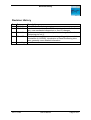
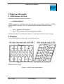
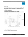
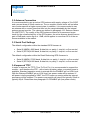
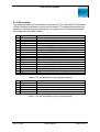
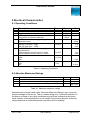
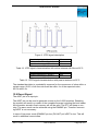
GPS Receiver A1030-A
A description of Tyco Electronics’
GPS module A1030-A
User’s Manual
Version 2.0
Hardware Revision 01
This page was intentionally left blank.
Revision History
Revision History
Rev. Date
1.0 06-22-04
1.1 17-09-04
1.2
18-11-04
2.0
07-14-05
Description
Initial Draft – Preliminary version
Introduced corrections from R&D, extensions towards functionality, new mechanical dimensions, a few I/O changes
Correct memory size, additional products, change in Dead
Reckoning pin out (!),
Detailed pin description, new orientation of layout (to match the
orientation of A1029-B), introduction of Dead Reckoning interface, generally more detailed information
mm-dd-yy
V2.0 - 07/05
User’s Manual
Page 3 of 37
Disclaimer
Disclaimer
THIS DOCUMENT CONTAINS PROPRIETARY INFORMATION OF TYCO ELECTRONICS CORPORATION/POWER SYSTEMS (TYCO ELECTRONICS). IT MAY
NOT BE COPIED OR TRANSMITTED BY ANY MEANS, PASSED TO OTHERS,
OR STORED IN ANY RETRIEVAL SYSTEM OR MEDIA, WITHOUT PRIOR
CONSENT OF TYCO ELECTRONICS OR ITS AUTHORIZED AGENTS.
THE INFORMATION IN THIS DOCUMENT IS, TO THE BEST OF OUR
KNOWLEDGE, ENTIRELY CORRECT. HOWEVER, TYCO ELECTRONICS CAN
NEITHER ACCEPT LIABILITY FOR ANY INACCURACIES, OR THE
CONSEQUENCES THEREOF, NOR FOR ANY LIABILITY ARISING FROM THE
USE OR APPLICATION OF ANY CIRCUIT, PRODUCT, OR EXAMPLE SHOWN IN
THE DOCUMENT.
THE PRODUCT (HARD- AND SOFTWARE) DESCRIBED IN THIS DOCUMENTATION IS NOT AUTHORIZED FOR USE IN LIFE SUPPORT DEVICES OR
SYSTEMS WITHOUT THE EXPRESS WRITTEN APPROVAL OF TYCO ELECTRONICS.
THIS DOCUMENT MAY PROVIDE LINKS TO OTHER WORLD WIDE WEB SITES
OR RESOURCES. BECAUSE TYCO ELECTRONICS HAS NO CONTROL OVER
SUCH SITES AND RESOURCES, TYCO ELECTRONICS SHALL NOT BE
RESPONSIBLE FOR THE AVAILABILITY OF SUCH EXTERNAL SITES OR
RESOURCES, AND DOES NOT ENDORSE AND IS NOT RESPONSIBLE OR
LIABLE FOR ANY CONTENT, ADVERTISING, PRODUCTS, OR OTHER
MATERIALS ON OR AVAILABLE FROM SUCH SITES OR RESOURCES. TYCO
ELECTRONICS SHALL NOT BE RESPONSIBLE OR LIABLE, DIRECTLY OR
INDIRECTLY, FOR ANY DAMAGE OR LOSS CAUSED OR ALLEGED TO BE
CAUSED BY OR IN CONNECTION WITH USE OF OR RELIANCE ON ANY SUCH
CONTENT, GOODS OR SERVICES AVAILABLE ON OR THROUGH ANY SUCH
SITE OR RESOURCE.
TYCO ELECTRONICS RESERVES THE RIGHT TO CHANGE, MODIFY, OR
IMPROVE THIS DOCUMENT OR THE PRODUCT DESCRIBED HEREIN, AS
SEEN FIT BY TYCO ELECTRONICS WITHOUT FURTHER NOTICE.
Page 4 of 37
User’s Manual
V2.0 - 07/05
Table of Contents
Table of Contents
1 Introduction ........................................................................................................ 7
1.1 Dead Reckoning................................................................................................ 7
1.2 Label ................................................................................................................. 8
1.3 Characteristics .................................................................................................. 8
1.4 Handling Precautions ........................................................................................ 8
2 Ordering Information ......................................................................................... 9
2.1 GPS Receiver A1030-A .................................................................................... 9
2.2 Packing ............................................................................................................. 9
2.3 Additional Equipment ...................................................................................... 10
2.3.1 Demonstration and Evaluation Kits .............................................................. 10
2.3.2 Development and Target Platforms.............................................................. 10
3 Quick Start........................................................................................................ 11
3.1 Minimum Configuration ................................................................................... 11
3.2 Antenna Connection........................................................................................ 12
3.3 Serial Port Settings ......................................................................................... 12
3.4 Improved TTFF ............................................................................................... 12
4 Mechanical Outline .......................................................................................... 13
4.1 Mechanical Overview ...................................................................................... 13
4.2 Connector ....................................................................................................... 13
5 Pin Out Information.......................................................................................... 14
5.1 Standard GPS and DR Firmware Configuration.............................................. 14
5.1.1 Layout .......................................................................................................... 14
5.1.2 Description ................................................................................................... 15
5.2 General Comments ......................................................................................... 16
5.3 Free Configuration .......................................................................................... 16
6 Dead Reckoning Interface ............................................................................... 19
6.1 Odometer and Reverse Signals ...................................................................... 19
6.2 Gyro and Gyro Signal...................................................................................... 20
6.3 Power Supply for Internal ADC ....................................................................... 21
7 Memory Map ..................................................................................................... 22
8 Electrical Characteristics ................................................................................ 23
8.1 Operating Conditions ...................................................................................... 23
8.2 Absolute Maximum Ratings ............................................................................ 23
9 Mounting........................................................................................................... 24
10 Use of Antenna............................................................................................... 25
10.1 Active Antenna .............................................................................................. 25
10.2 Passive Antenna ........................................................................................... 25
11 Quality and Reliability.................................................................................... 26
V2.0 - 07/05
User’s Manual
Page 5 of 37
Table of Contents
11.1 Environmental Conditions ............................................................................. 26
11.2 Product Qualification ..................................................................................... 26
11.3 Production Test ............................................................................................. 26
12 Applications and Hints .................................................................................. 27
12.1 Minimum Configuration ................................................................................. 27
12.2 Antenna Sensor Pin (ANTSTAT)................................................................... 27
12.3 Gain select pin (GS)...................................................................................... 27
12.4 VANT pin (antenna voltage input pin) ........................................................... 27
12.5 LOCK pin (position fix pin) ............................................................................ 28
12.6 ENABLE pin (low-power mode)..................................................................... 28
12.7 1PPS pin (1 pulse per second pin)................................................................ 28
12.8 Reset Signal.................................................................................................. 29
12.9 VBAT pin....................................................................................................... 30
12.10 Usage of additional interfaces ..................................................................... 30
12.10.1 I2C ........................................................................................................... 30
12.10.2 BSPI......................................................................................................... 30
12.10.3 HDLC ....................................................................................................... 31
12.10.4 CAN ......................................................................................................... 31
12.10.5 USB Slave Interface................................................................................. 31
13 Application Software ..................................................................................... 33
14 Demonstration and Evaluation Kit................................................................ 34
15 Related Information ....................................................................................... 35
15.1 Contact.......................................................................................................... 35
15.2 Related Documents....................................................................................... 35
16 List of Tables .................................................................................................. 37
17 List of Figures ................................................................................................ 37
Page 6 of 37
User’s Manual
V2.0 - 07/05
GPS Receiver A1030-A
1 Introduction
Tyco Electronics’ GPS module A1030-A is a highly integrated GPS receiver module. It is capable of receiving signals from up to 12 GPS satellites and transferring
them into position and timing information that can be read over a serial port. The
A1030 extends Tyco Electronics’ GPS receiver family based on the ST Microelectronics’ STA2051, already represented by the A1029-A and A1029-B. In addition to
these receivers, it offers additional Flash, SRAM and I/O and is therefore ideally
suited for customer applications. The A1030 basic firmware features high-end GPS
functionality at low power consumption. Major highlights of the module are:
•
•
•
•
•
•
•
•
•
•
4Mbit Flash and 2Mbit SRAM
Operable at 3.3V / 50mA @ 1fix per second
Antenna link cable with SMA connector
Antenna sensor pin with defined current sensing range (for antenna detection or antenna short circuit detection)
LNA Gain select pin (for adjustment to various RF signal conditions)
Current limiter (50mA) for active antennas
Hardware and software stand-by @ 500µA
Wait-for-IRQ @ 1mA
Battery back-up mode (RTC and SRAM supported)
Access to SPI, I2C, HDLC, CAN, USB, Smart Card interface with customer
software
This GPS receiver is available as an off-the-shelf component, 100% tested and
shipped in trays.
1.1 Dead Reckoning
The A1030 offers Dead Reckoning capability. The I/O connector allows connecting
to the necessary signals. This manual holds a detailed description on setting up a
Dead Reckoning solution.
V2.0 - 07/05
User’s Manual
Page 7 of 37
GPS Receiver A1030-A
1.2 Label
The A1030’s labels hold the following information:
Product code (A1030-A) with hardware version (01)
A1030-A-01
Firmware version (102-01), factory and date code
(week and year: 3105)
102-01 BZ/31/05
Figure 1: A1030 labels
1.3 Characteristics
The modules are characterized by the following parameters.
Channels
Frequency
Position Accuracy
Time To First Fix – TTFF
(theoretical minimum values; values in real world
may differ)
Mechanical dimensions
Stand alone
Differential
Obscuration recovery (1)
Hot start (2)
Warm (3)
Autonomous / cold (4) (6)
Power-off start (5) (6)
Length
Width
Height
Weight
12, parallel tracking
L1 (= 1575 MHz)
3m CEP (SA off)
< 2m CEP
1s
< 3s
< 32s
< 60s
Varying
39.37mm, 1.55”
35.56mm, 1.4”
6.7mm, 0.26”
11g, 0.4oz
Table 1: A1030-A characteristics
(1)
(2)
(3)
(4)
(5)
The calibrated clock of the receiver has not stopped, thus it knows precise time (to the µs level).
The receiver has estimates of time/date/position and valid almanac and ephemeris data.
The receiver has estimates of time/date/position and recent almanac.
The receiver has no estimate of time/date/position, and no recent almanac.
Receiver is powered off, clock stops. Start-up time depends on time passed since power-off and
power-on location.
(6) In order to improve TTFF, the receiver allows setting of time/date/position.
1.4 Handling Precautions
The GPS receiver A1030-A is a module that is sensitive to electrostatic discharge
(ESD). Please handle with appropriate care.
Page 8 of 37
User’s Manual
V2.0 - 07/05
GPS Receiver A1030-A
2 Ordering Information
2.1 GPS Receiver A1030-A
The order numbers are built as follows:
•
V23993A1030Axxx
V23993 stands for Tyco Electronics wireless and communication products, A1030A
for the A1030-A module. The “xxx” stands for the according firmware version.
Where
•
•
“1xx” is standard GPS software
“2xx” is GPS software with Dead Reckoning support
The functionality of both software versions is reflected in the according manuals.
2.2 Packing
The A1030-A comes in trays, with 12 modules per tray.
All dimensions in [mm]
Figure 2: A1030-A tray specifications
V2.0 - 07/05
User’s Manual
Page 9 of 37
GPS Receiver A1030-A
2.3 Additional Equipment
2.3.1 Demonstration and Evaluation Kits
V23993-DKS1030-A
V23993-DKS1030-B
V23993-DR1030-A
Demonstration and evaluation board (including one module
V23993-A1030-A) without LCD
Demonstration and evaluation board (including one module
V23993-A1030-A) with LCD
Dead Reckoning demonstration and evaluation system for testing
in vehicles; integrated gyro; external signals (odometer pulse,
forward/reverse) required.
Table 2: Demonstration and evaluation kits
2.3.2 Development and Target Platforms
V23993-DEV1030-A
V23993-DEV1030-B
V23993-DTK1030-A
Development platform incl. Rowley Toolset, hardware interface
adapter, demonstration and evaluation board without LCD, libraries, sample code, description.
Development platform incl. Rowley Toolset, hardware interface
adapter, demonstration and evaluation board with LCD, libraries,
sample code, description.
Development platform incl. Rowley Toolset, hardware interface
adapter, libraries, sample code, description.
Table 3: Development platforms
Detailed descriptions of the additional kits can be found in the according manuals.
Page 10 of 37
User’s Manual
V2.0 - 07/05
GPS Receiver A1030-A
3 Quick Start
In order to allow an easy and quick start with the GPS module A1030-A, this chapter provides a short overview on the most important steps to receive NMEA messages with position information on a serial port. For details please refer to the according chapters.
3.1 Minimum Configuration
The following picture shows a recommended minimum configuration for NMEA output and commands received and sent via an RS232 interface.
Figure 3: Recommended minimum configuration
Remarks:
•
•
Place C1 to C5 close to MAX3232. For capacity values see datasheet of actual component used.
Use 3.3V level shifter (MAX323 or equivalent).
V2.0 - 07/05
User’s Manual
Page 11 of 37
GPS Receiver A1030-A
3.2 Antenna Connection
It is recommended to use an active GPS antenna with supply voltage of 3 to 5VDC
and a current draw of 50mA maximum. The on-module current limiter will not allow
use of antennas with a higher current draw. In addition, it is recommended to use
an antenna with a current draw that falls into the range detectable by the internal
antenna current monitor. The values are defined in paragraph 12.2 Antenna Sensor
Pin (ANTSTAT). The quality of the GPS antenna chosen is of paramount importance for the overall sensitivity of the GPS system. An active antenna should have a
gain ≥ 20dB and a noise figure ≤ 1.5dB, which applies to more than 95% of the antennas available in the market.
3.3 Serial Port Settings
The default configuration within the standard GPS firmware is:
•
•
Serial 0 (NMEA) 4800 baud, 8 data bits, no parity, 1 stop bit, no flow control
Serial 2 (RTCM) 4800 baud, 8 data bits, no parity, 1 stop bit, no flow control
The default configuration within the Dead Reckoning GPS firmware is:
•
•
Serial 0 (NMEA) 57600 baud, 8 data bits, no parity, 1 stop bit, no flow control
Serial 2 (RTCM) 4800 baud, 8 data bits, no parity, 1 stop bit, no flow control
3.4 Improved TTFF
In order to improve the TTFF (Time To First Fix), it is recommended to support the
module – and therefore the RTC - with a back-up battery when no system power is
available. Standard operation mode is entered with the ENABLE pin on HIGH level.
With the Wakeup ENABLE pin on LOW level, low power mode will be entered. If
still power is being supplied to VBAT, the RTC keeps on running while the internal
processors will be stopped. The power consumption will drop from typically 50mA to
typically 30µA. Please see also paragraph 12.6 ENABLE pin (low-power mode).
Page 12 of 37
User’s Manual
V2.0 - 07/05
GPS Receiver A1030-A
4 Mechanical Outline
4.1 Mechanical Overview
All dimensions in [mm]
Figure 4: Mechanical outline (bottom view)
4.2 Connector
The power and I/O connector used on the A1030-A is a 1.27mm (0.05”) low profile,
double row socket with a height of 2.21mm (.087”) and a total of 50 contacts. Potential counterparts on the motherboard are e.g. Harwin 1.27mm (0.05”) micro strips
of the M50 series.
V2.0 - 07/05
User’s Manual
Page 13 of 37
GPS Receiver A1030-A
5 Pin Out Information
The functionality of the pins can be configured by software. This chapter describes
the pin out configuration with Tyco standard GPS firmware including the pin out for
a Dead Reckoning configuration and possible configurations with different interfaces.
5.1 Standard GPS and DR Firmware Configuration
5.1.1 Layout
Figure 5: Pin out information (bottom and top view)
Bottom view is showing the side of the module that will face the carrier board.
Page 14 of 37
User’s Manual
V2.0 - 07/05
GPS Receiver A1030-A
5.1.2 Description
This table describes the functionality of the pins with Tyco Standard GPS firmware
or Dead Reckoning firmware running on the module. The associated symbols are
explained. General-purpose pins that are not supported in the standard firmware
are explained further down below.
Pin
1
3
5
7
9
11
13
19
21
23
29
33
37
39
41
45
47
49
Symbol
GND
Vcc
VBAT
ENABLE
nRST
Rx0
Tx0
Rx2
Tx2
TEST0
Vgyro
LOCK
GS
ANTSTAT
VANT
Vcc3A
Odo
F/R
Description
Ground (power supply)
+3.3V (power supply)
Back-up battery supply pin (RTC and SRAM)
Enable pin – low power when low
Reset input
Serial input 0, NMEA in
Serial output 0, NMEA out
Serial input 2, RTCM input (DGPS)
Serial output 2
Reserved for test purposes
Input pin for gyro output voltage (required for DR)
Activated on LOCK (position fix)
Gain Select for LNA – leave open
Antenna sensor output
Power supply Antenna external
Analog voltage supply < +3.3V (required for DR)
Odometer input (required for DR)
Reverse signal input (required for DR)
Table 4: Pin out description (odd signal numbers)
Pin
2
10
46
48
50
Symbol
Res.
1PPS
Res.
Res.
Res.
Description
Reserved for future use – do not connect
1PPS (pulse per second) output
Reserved for future use – do not connect
Reserved for future use – do not connect
Reserved for future use – do not connect
Table 5: Pin out description (even signal numbers)
V2.0 - 07/05
User’s Manual
Page 15 of 37
GPS Receiver A1030-A
5.2 General Comments
The following comments should be considered for a design with and use of the
module:
•
•
•
•
Standard configuration of serial port (no DR software):
Serial 0 (NMEA) 4800 baud, 8 data bits, no parity, 1 stop bit, no flow control
Serial 2 (DGPS) 4800 baud, 8 data bits, no parity, 1 stop bit, no flow control
Standard configuration of serial port (with DR software):
Serial 0 (NMEA) 57600 baud, 8 data bits, no parity, 1 stop bit, no flow control
Serial 2 (DGPS) 4800 baud, 8 data bits, no parity, 1 stop bit, no flow control
Gain Select
Default setting is “open” (identical to logical low), which results in a high gain
(14dB). This setting is recommended.
nRST
Do not pull low when in low power mode
5.3 Free Configuration
For custom specific applications, all pins are more or less user definable. The final
function of a pin is determined by software running in the STA2051 (Vespucci).
Please refer also to chapter “12.10 Usage of additional interfaces” and for detailed
information to the STMicroelectronic STA2051 Vespucci User Manual.
The following tables describe the pin numbers “Pin”, the function of the pin as a
specific function of the A1030-A or as configured in the standard or Dead Reckoning firmware “Function”, the according pin on the STA2051 (Vespucci) “STA2051”,
the direction of the signal “Dir.”, and the description of the according functionality
”Description”.
Page 16 of 37
User’s Manual
V2.0 - 07/05
GPS Receiver A1030-A
Pin Function
STA2051
1
3
5
7
9
GND
Vcc33
VBAT
ENABLE
nRST
nRSTIN
11
Rx0
P0.8
13
Tx0
P0.9
I
V33
P0.10
17
P0.11
19
Rx2
P0.13
21
Tx2
P0.14
23
TEST0
BOOTEN
25
P1.4
27
P1.5
29
P1.0
31
P1.1
33
P1.2
35
P1.3
GS
ANTSTAT
VANT
43
I
Digital Supply Voltage for I/O circuitry (3.3 Volt)
I
A1030 specific: Battery back-up pin for RTC and SRAM
I
15
37
39
41
Dir. Description
I
I/O
I
O
I/O
I
O
I/O
I
O
I/O
I
O
I/O
I
O
I/O
I
O
I
I/O
I
I
I/O
I
O
I/O
O
AI
I/O
I
AI
I/O
O
AI
I/O
I
AI
I
O
P0.12
45
Vcc3A
VDD
47
Odo
P0.6
49
F/R
P0.7
I
I/O
O
I
I/O
I/O
I/O
I
Reset Input with Schmitt-Trigger characteristics and noise filter.
General Purpose I/O
U0.RX: UART 0 - Receive Data Input
U0.TX: UART 0 - Transmit Data Output
General Purpose I/O
BOOT.0 - Special BOOT configuration select
U0.TX: UART 0 - Transmit Data Output
General Purpose I/O
U1.RX: UART 1 - Receive Data Input
U1.TX: UART 1 - Transmit Data Output
General Purpose I/O
BOOT.1 - Special BOOT configuration select
U1.TX: UART 1 - Transmit Data Output
General Purpose I/O
U2.RX: UART 2 - Receive Data Input
T2.OCMPA: Extended Function Timer 2 - Output Compare A
General Purpose I/O
T2.ICAPA: Extended Function Timer 2 - Input Capture A
U2.TX: UART 2 - Transmit Data Output
Enables sampling of BOOT[1:0] pins on exit from external Reset
General Purpose I/O
T1.ICAPA: Ext. Funct. Timer 1 - Input Capture A or External Clock
HTXACT: HDLC - Transmit Buffer Active
General Purpose I/O
T1.ICAPB: Extended Function Timer 1 - Input Capture B
HOVSCLK: HDLC - oversampling Clock Out
General Purpose I/O
T3.OCMPB: Extended Function Timer 3 - Output Compare B
AIN0: ADC - Analog Data Input 0
General Purpose I/O
T3.ICAPA: Ext. Funct. Timer 3 - Input Capture A or External Clock
AIN1: ADC - Analog Data Input 1
General Purpose I/O
T3.OCMPA: Ext. Function Timer 3 - Output Compare A or PWM
AIN2: ADC - Analog Data Input 2
General Purpose I/O
T3.ICAPB: Extended Function Timer 3 - Input Capture B
AIN3: ADC - Analog Data Input 3
Gain select (open = default = high gain)
Antenna status
Antenna voltage supply
General Purpose I/O
SCCLK: Smart Card - Reference Clock Output
Analog Supply Voltage for the A/D Converter
General Purpose I/O
S0.SCLK: BSPI 1 - Serial Clock
General Purpose I/O
S1.SSN: BSPI 1 - Slave Select
Table 6: A1030 odd pins
V2.0 - 07/05
User’s Manual
Page 17 of 37
GPS Receiver A1030-A
Pin Function
2
Res.
STA2051
P0(2)
4
P0(3)
6
P1(6)
8
P1(7)
10
1PPS
P1(8)
12
P1(9)
14
P1(10)
16
P1(11)
18
P1(12)
20
P1(13)
22
P1(14)
24
P1(15)
26
P2(8)
28
P2(9)
30
P2(10)
32
P2(11)
34
36
38
40
42
44
P2(12)
P2(13)
P2(14)
P2(15)
USBDP
USBDN
46
Res.
P0(4)
48
Res.
P0(0)
50
Res.
P0(1)
Dir. Description
I/O
I/O
I/O
I/O
I/O
O
I/O
O
I/O
O
I/O
O
I/O
O
I/O
I
I/O
I
I/O
O
I/O
I/O
I
I/O
I/O
I
I/O
O
I/O
I
I/O
I
I/O
I
I/O
I
I/O
General Purpose I/O
S0.SCLK: BSPI 0 - Serial Clock
I1.SCL: I2C - Serial Clock
General Purpose I/O
I1.SDA: I2C - Serial Data
S0.SSN: BSPI 0 - Slave Select
General Purpose I/O
T1.OCMPB: Extended Function Timer 1- Output Compare B
General Purpose I/O
T1.OCMPA: Ext. Function Timer 1- Output Compare A or PWM
General Purpose I/O
PPS: GPS Pulse Per Second
General Purpose I/O
PRN: GPS Pseudo-Random Sequence generator (PRN11)
General Purpose I/O
USBCLK – 48Mhz clock for USB interface
General Purpose I/O
CANRX: CAN – Receive Data Input
General Purpose I/O
CANTX: CAN - Transmit Data Output
General Purpose I/O
I0.SCL: I2C – Serial Clock
HCLK – HDLC reference clock
General Purpose I/O
I1.SDA: I2C - Serial Data
HRXD - HDLC - Receive Data Input
General Purpose I/O
HTXD – HDLC – Transmit Data Output
General Purpose I/O
INT2: External Interrupt - Input Channel 2
General Purpose I/O
INT3: External Interrupt – Input Channel 3
General Purpose I/O
INT4: External Interrupt - Input Channel 4
General Purpose I/O
INT5: External Interrupt – Input Channel 5
General Purpose I/O
I/O
General Purpose I/O
I/O
General Purpose I/O
I/O
General Purpose I/O
I/O
USB Serial line – Positive
I/O
I/O
I/O
I/O
I/O
O
I/O
I/O
O
USB Serial line – Negative
General Purpose I/O
S1.MISO: BSPI 1 - Master Input / Slave Output
General Purpose I/O
S0.MISO: BSPI 0 – Master Input / Slave Output
U3.TX: UART 3 – Transmit Data Output
General Purpose I/O
S0.MOSI: BSPI 0 - Master Output / Slave Input
U3.RX: UART 3 - Receive Data Input
Table 7: A1030 even pins
Page 18 of 37
User’s Manual
V2.0 - 07/05
GPS Receiver A1030-A
6 Dead Reckoning Interface
Dead Reckoning (DR) functionality requires the correct firmware (“2xx”) and the
correct hardware set-up on the main board. Two digital signals (odometer and reverse), a gyro and according power supply for the internal ADC are necessary to
support this feature. This chapter shall provide all necessary information for designing an according main board. The recommendations here assume the availability of
a 5V (VCC5D) and 3.3V (VCC3D) digital power supply on this main board.
6.1 Odometer and Reverse Signals
Both signals are provided by the vehicle. In order to connect the signals in the correct way to the module, they should be optically isolated. The following schematic is
an example on how an implementation could look like.
Figure 6: Connecting an odometer signal
The same configuration can be used for the reverse signal.
V2.0 - 07/05
User’s Manual
Page 19 of 37
GPS Receiver A1030-A
6.2 Gyro and Gyro Signal
The gyro is of utmost importance for the performance of the DR system. The following data shall provide a guideline for selecting the right gyro:
Basic gyro data
• Supply voltage: 5V (more gyros available, also used in the example) or 3V
• Current draw: < 20mA
• Max. angular velocity: ± 80 deg / s
• Output at angular velocity 0: 1.5V (or 2.5V and according divider, as shown
in the example)
• Resolution: ~ 0.1 deg / s
• Scale factor: ~ 25mV / deg / s (smaller values possible, e.g. 12.5mV / deg / s
at supply voltage 3V)
Important for system performance as well:
• Temperature coefficient of scale factor: max. ± 10% at -30° to +80°C
• Linearity: ± 0.5% full scale
• Offset drift: e.g. for ENV-05G Murata: 9 deg / s (smaller values desirable)
• Response: max. 10Hz
• Noise level; max. 10mVp-p
In the example (also the DR1030A board), the Murata ENV-05G is used, a 5V gyro
with an output of 2.5V at 0°/s angular velocity. To allow the complete output range
to fit into the input range of the internal ADC, a 2:1 divider is used.
Figure 7: Connecting a gyro and the gyro signal
Page 20 of 37
User’s Manual
V2.0 - 07/05
GPS Receiver A1030-A
6.3 Power Supply for Internal ADC
The internal ADC requires a separate power supply on pin Vcc3A. The power
should be derived from the same source that is used for the gyro. This way, oscillations of the power source affect the gyro and the ADC and therefore minimize the
negative effects. It is also recommended that Vcc3A is slightly below the power
supplied to module (Vcc).
The following circuit shows an example on how to generate the power for the internal ADC from a 5V source.
Figure 8: Power supply for internal ADC (Vcc3A)
V2.0 - 07/05
User’s Manual
Page 21 of 37
GPS Receiver A1030-A
7 Memory Map
Beside the internal register, RAM and Flash access, the module offers – depending
on its version) additional external Flash and / or SRAM. The external memory is
addressed via a 16bit interface at the following addresses:
Memory type Address
Flash
SRAM
0x60000000
0x62000000
Table 8: External memory map
A theoretical total of a memory space of 224 bytes (corresponding to 16 Mbytes or
128 Mbit) of SRAM and Flash respectively can be addressed. Not existing memory
is simply mirrored. For example the Flash memory of a module equipped with 8Mbit
will be seen at address 0x60000000, 0x60100000, 0x60200000, and so on.
For information on the internal memory map, please refer to STMicroelectronics
Vespucci User Manual.
Page 22 of 37
User’s Manual
V2.0 - 07/05
GPS Receiver A1030-A
8 Electrical Characteristics
8.1 Operating Conditions
Pin
Description
Min
Typical
Max
3
Vcc
Current draw (without active Antenna)
Input current in standby mode
1 PPS (1 pulse per second), reference GPS
time (active and passive antenna)
VANT (active antenna supply voltage)
Antenna current
GS (gain select for LNA), input pin
GS high (Low gain – 4dB)
GS low (high gain – 14dB)
ANTSTAT (antenna sensor output) @ 1mA
current source
High at antenna current from 9 to 16mA
Low at antenna current <9mA or >16mA
Output pins
VOH
VOL
Input pins
VIH
VIL
3.0V
3.3V
50mA
30µA
+120ns
+90ns
3.6V
10
41
37
39
Vcc-0.5V
5.2V
50mA
Vcc-0.6V
Vcc
0.6V
Vcc-0.5V
0
Vcc
0.5V
Vcc-0.8V
0.4V
0.7Vcc
0.3Vcc
Table 9: Operating Conditions
8.2 Absolute Maximum Ratings
Pin
3
Description
Vcc
Current Antenna, external power supply
Applied voltage to all input pins excluding Vcc, VANT
Min
-0.3V
-0.3V
Max
3.6V
50mA
Vcc+0.3V
max. 3.6V
Table 10: Absolute maximum ratings
Stresses beyond those listed under “Absolute Maximum Ratings” may cause permanent damage to the device. This is a stress rating only. Functional operation of
the device at these or any other conditions beyond those indicated in the operational sections of this specification is not implied. Exposure to absolute maximum
rating conditions for extended periods may affect device reliability.
V2.0 - 07/05
User’s Manual
Page 23 of 37
GPS Receiver A1030-A
9 Mounting
This chapter covers the mounting of the A1030-A. The A1030-A offers a power and
I/O connector with a 1.27mm (0.05”) low profile, double row socket with a total of 50
contacts. Potential counterparts on the motherboard are Harwin 1.27mm (0.05”)
micro strips of the M50 series. For fixing the A1030-A on a motherboard appropriate
screws and bolts or clips (see also chapter 4.1 Mechanical Overview ff.) are recommended.
Page 24 of 37
User’s Manual
V2.0 - 07/05
GPS Receiver A1030-A
10 Use of Antenna
10.1 Active Antenna
General GPS active antenna specification:
Limitations:
•
•
Supply voltage according to voltage fed into VANT pin (5V max.)
Supply current 50mA (max.)
Recommendations:
•
•
Gain ≥ 20dB
Noise figure ≤ 1.5dB
The recommendations apply to the majority of active antennas that can be found in
the market. Anyhow, the quality of the GPS antenna chosen is of paramount importance for the overall sensitivity of the GPS system.
The system design needs to reflect the supply voltage of the antenna. If the supply
voltage is equal to Vcc, Vcc can be connected to VANT. If the antenna requires a
different supply voltage, the antenna bias can be provided through the VANT pin.
10.2 Passive Antenna
NOTE: Different passive antenna set-ups have been tested with positive results on
the performance of the A1030-A module. Anyhow, it is the responsibility of the system integrator to qualify the final configuration.
Please consider that it is crucial to keep the connection from the antenna to the
ANT pin as short as possible. Each bit of attenuation between the passive antenna
and the ANT pin will degrade GPS performance.
Recommendations:
•
•
Antenna gain: >2dBi
Antenna gain: < 2dBi / LNA close to the antenna recommended!
Please make sure that the antenna is properly tuned to its dielectric environment.
V2.0 - 07/05
User’s Manual
Page 25 of 37
GPS Receiver A1030-A
11 Quality and Reliability
11.1 Environmental Conditions
Operating temperature
Operating humidity
MSL JEDEC
(Moisture Sensitivity Level)
Storage
- 40 … + 85°C
Max. 85% r. H., non-condensing, at 85°C
3
6 months in original package.
Table 11: Environmental conditions
11.2 Product Qualification
Prior to product qualification the GPS receiver is preconditioned according to
EIA/JEDEC standard JESD22-A113-B / Level 3.
Basic qualification tests:
•
•
•
•
•
•
Temperature Cycling -40 … +85°C
Temperature Humidity Bias 85°C / 85% RH
High / Low Temperature Operating –40° / +85°C
High Temperature Operating Life +85°C
Vibration Variable Frequency
Mechanical Shock
Please contact Tyco Electronics for detailed information.
11.3 Production Test
Each module is electrically tested prior to packing and shipping to ensure state of
the art GPS receiver performance and accuracy.
Page 26 of 37
User’s Manual
V2.0 - 07/05
GPS Receiver A1030-A
12 Applications and Hints
12.1 Minimum Configuration
Please refer to chapter 3.1 Introduction for details. In addition, for optimized start-up
behavior it is strongly recommended to provide power at the VBAT pin when pulling
the ENABLE pin to LOW. This will improve start-up times after wake-up!
12.2 Antenna Sensor Pin (ANTSTAT)
The Antenna Sensor pin is an output pin. It provides correct status information for
an active GPS antenna with current consumption in the defined range! For an active antenna with a current consumption outside this range, an external circuit could
detect the connection or a disconnection or a short circuit.
•
•
•
Logic low when:
Logic high when:
Logic low when:
Iant < 9mA
9mA > Iant < 16mA
Iant > 16mA
Iant = DC current of GPS antenna (DC current through sensing resistor on GPS
module)
The Antenna Sensor pin can detect when an active antenna is connected. It can
also detect when the antenna is short-circuited or disconnected for some reason.
Please consider that the Antenna Sensor can provide no useful output when the
GPS antenna is fed externally, i.e. the VANT pin is not used (the sensing resistor
on the GPS module can not sense any DC current).
12.3 Gain select pin (GS)
The LNA Gain Select pin is an input pin.
•
•
Pin at GND (low) or open: LNA Gain 14dB (default)
Pin at Vcc (high): LNA Gain 4dB
It is recommended to leave the pin unconnected. This allows for amplification of
weaker signals and a firmware implementation of an automatic gain control (AGC)
function.
12.4 VANT pin (antenna voltage input pin)
The VANT pin is an input pin.
The supply voltage for an active GPS antenna has to be fed into the VANT pin.
The easiest way to do that is to connect Vcc to VANT. The maximum current is
50mA. A current limiter is integrated on the module.
V2.0 - 07/05
User’s Manual
Page 27 of 37
GPS Receiver A1030-A
12.5 LOCK pin (position fix pin)
The LOCK pin is an output pin.
When there is no valid position fix, the signal on the pin will be a continuous logic
low. During a valid position fix phase, the output signal will be a continuous logic
high.
This function is provided with the standard firmware only.
12.6 ENABLE pin (low-power mode)
The ENABLE pin is an input pin.
For enabling normal operation of the module, the pin has to be on HIGH level (e.g.
connected to Vcc). When the ENABLE pin is pulled down to GND, the module will
go to a low power mode where only the RTC will be supported (if a power source is
still connected to VBAT). I.e. date and time will be valid after wake-up. The current
draw will fall from typically 50mA to typically 30µA. Do not pull down low nRST at
the same time! This is not necessary and will result in additional current draw!
12.7 1PPS pin (1 pulse per second pin)
The 1PPS pin is an output pin.
In addition to precise positioning, GPS also allows for accurate timing due to the
synchronized atomic clocks in the GPS satellites. While the current date and time is
transmitted in NMEA sentences, an exact and accurate timing signal is provided via
the 1PPS pin of the A1030A module.
The 1PPS signal is valid only, whenever the GPS modules provide a valid position
fix. Therefore it is recommended to monitor the LOCK signal in parallel (or logically
AND the 1PPS and LOCK signals).
The rising edge of the signal is synchronized to GPS time and therefore also to
UTC. The 1PPS signal is characterized (a) by the delay “d” between the start of a
GPS second and the rising edge of the 1PPS and (b) by standard deviation of this
delay providing a measure for the stability or jitter of this signal. Additionally, the
duration “l” of the signal is outlined.
Page 28 of 37
User’s Manual
V2.0 - 07/05
GPS Receiver A1030-A
Figure 9: 1PPS signal description
Signal delay d (typical)
Standard deviation σd (typical)
Signal duration l (typical)
130ns
20ns
500ms
Table 12: 1PPS signal characterization with active antenna with filter at 22°C
Signal delay d (typical)
Standard deviation σd (typical)
Signal duration l (typical)
90ns
20ns
500ms
Table 13: 1PPS signal characterization with passive antenna at 22°C
The standard deviation is a probability measure for the occurrence of value within a
certain range. 68.3% of all new values will be within 1σ of the expected value,
95.5% within 2σ.
12.8 Reset Signal
The nRST pin is an input pin.
The nRST pin can be used to generate a reset on the A1029 modules. Resetting
the module will result in a restart of the complete firmware including the boot loader.
All information stored in flash memory will still be valid. The RTC will keep on running. The same result can be achieved using the ENABLE pin. Therefore connecting nRST is not necessary.
In case of low power mode (ENABLE pin low) DO NOT pull nRST to low. This will
result in additional current draw.
V2.0 - 07/05
User’s Manual
Page 29 of 37
GPS Receiver A1030-A
12.9 VBAT pin
The VBAT pin is an input pin.
The module will draw current from the VBAT pin whenever Vcc will be LOW. The
module will fall to stand-by mode and the RTC will keep on running. At the same
time, the external (only!) is backed.
12.10 Usage of additional interfaces
Additional interfaces can be used when writing specific software for the A1030. The
most commonly used interfaces for the module are I2C, BSPI, HDLC, CAN and
USB. Not all interfaces can be used simultaneously. Two I2C Interfaces are available. One of them is multiplexed with one BSPI interface, while the other is multiplexed with the HDLC; hence either one I2C + two BSPI, or two I2C + one BSPI, or
one I2C, one BSPI and the HDLC, or two BSPI and the HDLC are available at any
time. CAN and USB interfaces are independent of the other interfaces. For more
details please refer to according chapters in the STMicroelectronic Vespucci User
Manual.
12.10.1 I2C
The I2C Bus Interface serves as an interface between the microcontroller and the
external serial I2C bus. It provides both multi-master and slave functions, and controls all I2C bus-specific sequencing, protocol, arbitration and timing. It supports fast
I2C mode (400kHz).
A1030A: I2C interface one is realized via pin 02 (P0.2 – Serial Clock) and pin 04
(P0.3 - Serial Data), while interface two is realized via pin 20 (P1.13 – Serial Clock)
and pin 22 (P1.14 - Serial Data).
12.10.2 BSPI
The BSPI block is a standard 4-pin Serial Peripheral Interface for inter-IC control
communication. It interfaces on one side to the SPI bus and on the other has a
standard register data and interrupt interface.
The BSPI contains two 10-word x 16-bit FIFO’s one for receive and the other for
transmit. The BSPI can directly operate with words 8 and 16 bit long and generates
vectored interrupts separately for receive and transmit events.
A1030A: On the A1030, only one BSPI interface is completely available:
48: P0.0 - MISO
50: P0.1 - MOSI
02: P0.2 - SCLK
04: P0.3 - SSN
Page 30 of 37
User’s Manual
V2.0 - 07/05
GPS Receiver A1030-A
12.10.3 HDLC
The HDLC interface supports both the Telepass protocol and the European TC278
DSRC communication standard. It supports Full Duplex operating mode with independent baudrates for transmit/receive, including PLL for clock recovery. It features
NRZ, NRZI, Manchester encoding, automatic bit stuffing, FCS generation and CRC
check. Packets are stored in a local dual-port memory, for later retrieval by the
CPU; this buffer is sized to hold a full HDLC frame, to minimize CPU load during the
transaction.
A1030A: The HDLC interface pins are realized in the following way:
25: P1.4 - Transmit Buffer Active
27: P1.5 - Oversampling Clock Out
20: P1.13 - Reference Clock
22: P1.14 - Receiver Data Input
24: P1.15 - Transmit Data Output
12.10.4 CAN
The C-CAN consists of the components CAN Core, Message RAM, Message Handler, Control Registers, and Module Interface. The CAN Core performs communication according to the CAN protocol version 2.0 part A and B. The bit rate can be
programmed to values up to 1MBit/s. For the connection to the physical layer additional transceiver hardware is required. For communication on a CAN network, individual Message Objects are configured. The Message Objects and Identifier Masks
for acceptance filtering of received messages are stored in the Message RAM.
All functions concerning the handling of messages are implemented in the Message
Handler. Those functions are the acceptance filtering, the transfer of messages between the CAN Core and the Message RAM, and the handling of transmission requests as well as the generation of the module interrupt. The register set of the CCAN can be accessed directly by the CPU via the module interface. These registers
are used to control/configure the CAN Core and the Message Handler and to access the Message RAM.
A1030A: The CAN signals CAN-TX and CAN-RX are realized on pins 18 and 16,
respectively.
12.10.5 USB Slave Interface
The USB_IP Peripheral provides an USB compliant connection between the host
PC and the function implemented inside the ARM device. Data transfers between
host PC and system memory occur through a dedicated packet buffer memory accessed directly by the USB_IP peripheral. This dedicated buffer memory must be
sized according to the number of used endpoints and their related maximum packet
sizes. In this implementation the dedicated memory is sized to 512 Byte and up to 8
V2.0 - 07/05
User’s Manual
Page 31 of 37
GPS Receiver A1030-A
endpoints can be used. The USB_IP interfaces with the USB host and detects token packets, handles data transmission/reception, and processes handshake packets as required by the USB standard. Transaction formatting is performed by hardware, including CRC generation and checking.
Each endpoint is associated with a buffer description block indicating where the
endpoint related memory area is located, how large it is or how many bytes must be
transmitted. When a token for a valid function/endpoint pair is recognized by the
USB_IP, the related data transfer (if required and if the endpoint is configured)
takes place, with the USB_IP buffering data loaded in an internal 16 bit long register, and performing memory access to the dedicated buffer. When all data have
been transferred, if needed, the proper handshake packet over the USB is generated or expected, according to the direction of the transfer. At the end of the transaction, an endpoint specific interrupt is generated: reading status registers and/or
using different interrupt response routines, the microcontroller can determine which
endpoint has to be served, which type of transaction took place, if errors occurred
(bit stuffing, format, CRC, protocol, missing ACK, over/underrun, etc....). Special
support is offered to isochronous transfers and high throughput bulk transfers, implementing a double buffer usage which allows having always an available buffer
for the USB_IP while the microcontroller uses the other one.
The unit can be placed in low-power mode (SUSPEND mode), by writing in a control register whenever required. At this time, all static power dissipation is avoided,
and the macrocell clock can be slowed down or stopped. The detection of activity at
the USB inputs while in low-power mode wakes the device up asynchronously. A
special interrupt source can be connected directly to a wake-up line so as to allow
the system to immediately restart normal clock generation and/or support direct
clock start/stop.
A1030A: USBDN is available on pin 44 and USBDP on pin 42. The 48MHz USB
clock has to be provided on pin 14 (P1.10).
Page 32 of 37
User’s Manual
V2.0 - 07/05
GPS Receiver A1030-A
13 Application Software
Tyco Electronics provides Standard GPS Software that covers the following basic
functions of a GPS module:
-
Standard GPS functionality
Dead Reckoning capability
WAAS/EGNOS support
Data logging
For details, please refer to the GPS Firmware manuals.
V2.0 - 07/05
User’s Manual
Page 33 of 37
GPS Receiver A1030-A
14 Demonstration and Evaluation Kit
For demonstration and easy evaluation of GPS performance Tyco Electronics offers
a Demonstration and Evaluation Kit (including one GPS A1030-A module). It shows
two serial interfaces (NMEA and RTCM). The kit can be powered by an external 5
to 12V source. Accompanied by an antenna and serial cable it offers a ready-to-go
set.
This platform is also feasible as a target for custom specific developments. With its
standard JTAG interface, programming toolsets by ARM (RealView) or Rowley
(CrossWorks for ARM) can be used. It offers access to all I/O pins.
In addition, a Dead Reckoning test platform in a closed housing is available. This kit
allows a wide power input range (7V to 32V) and avoids problems in an electrically
dirty environment and makes the unit ideal for testing in vehicles.
For further information please contact Tyco Electronics.
Page 34 of 37
User’s Manual
V2.0 - 07/05
GPS Receiver A1030-A
15 Related Information
15.1 Contact
This manual was created with due diligence. We hope that it will be helpful to the
user to get the most out of the GPS module.
Anyway, inputs about errors or mistakable verbalizations and comments or proposals to TYCO Electronics, Power Systems in Munich, Germany, for further improvements are highly appreciated.
Hans Wiedemann
Product Marketing Manager
Positioning Products
Tel.: +49 89 6089 838
Fax: +49 89 6089 835
Tyco Electronics Corporation
Power Systems
Finsinger Feld 1
85521 Ottobrunn, Germany
Email to [email protected].
Please visit our website at www.tycoelectronics.com/gps.
15.2 Related Documents
•
•
•
•
•
Manual: T.E. GPS Firmware A1030 (TYCO)
Manual: T.E. GPS Firmware DR A1030 (TYCO)
Manual: T.E. GPS DemoKit DKS1030AB (TYCO)
Manual: T.E. GPS Dead Reckoning Kit DR1030A (TYCO)
Manual: STA2051 - Vespucci (STM)
V2.0 - 07/05
User’s Manual
Page 35 of 37
GPS Receiver A1030-A
This page was intentionally left blank.
Page 36 of 37
User’s Manual
V2.0 - 07/05
Lists of Tables
and Figures
16 List of Tables
Table 1: A1030-A characteristics ............................................................................. 8
Table 2: Demonstration and evaluation kits ........................................................... 10
Table 3: Development platforms ............................................................................ 10
Table 4: Pin out description (odd signal numbers) ................................................. 15
Table 5: Pin out description (even signal numbers) ............................................... 15
Table 6: A1030 odd pins ........................................................................................ 17
Table 7: A1030 even pins ...................................................................................... 18
Table 8: External memory map .............................................................................. 22
Table 9: Operating Conditions ............................................................................... 23
Table 10: Absolute maximum ratings ..................................................................... 23
Table 11: Environmental conditions ....................................................................... 26
Table 12: 1PPS signal characterization with active antenna with filter at 22°C...... 29
Table 13: 1PPS signal characterization with passive antenna at 22°C .................. 29
17 List of Figures
Figure 1: A1030 labels ............................................................................................. 8
Figure 2: A1030-A tray specifications....................................................................... 9
Figure 3: Recommended minimum configuration................................................... 11
Figure 4: Mechanical outline (bottom view)............................................................ 13
Figure 5: Pin out information (bottom and top view)............................................... 14
Figure 6: Connecting an odometer signal .............................................................. 19
Figure 7: Connecting a gyro and the gyro signal.................................................... 20
Figure 8: Power supply for internal ADC (Vcc3A) .................................................. 21
Figure 9: 1PPS signal description .......................................................................... 29
V2.0 - 07/05
User’s Manual
Page 37 of 37