1
ADSP-216x
ADSP-2165/ADSP-2166
CLOCK OR
CRYSTAL
CLKIN
XTAL
CLKOUT
3
4
VDD
GND
SERIAL
PORT 0
RESET
IRQ2
ADSP-216x
BR
SCLK
RFS
TFS
DT
DR
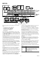
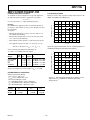
When MMAP = 0, on-chip program memory ROM occupies
12K words beginning at address 0x0000. Internal program
memory RAM occupies 1K words beginning at address 0x3000.
Off-chip program memory uses the 2K words beginning at
address 0x3800. The ADSP-2165/ADSP-2166 does not support
boot memory.
SERIAL
DEVICE
(OPTIONAL)
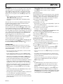
When MMAP = 1, 2K words of off-chip program memory begin
at address 0x0000. 10K words of on-chip program memory
ROM at 0x800 to 0x2FFF, and the remainder 2K words of
program memory ROM is at 0x3800 to 0x3FFF. Internal program memory RAM occupies 1K words at address 0x300 to
0x33FF.
SCLK
RFS OR IRQ0
BG
SERIAL
PORT 1
MMAP
PMS
RD RW ADDRESS DATA DMS BMS
14
TFS OR IRQ1
DT OR FO
SERIAL
DEVICE
(OPTIONAL)
DR OR FI
2K
EXTERNAL
D23-8
16
A D CS
OE
WE
PROGRAM
MEMORY
(OPTIONAL)
A
OE
D
0x0000
0x0000
24
0x07FF
0x0800
12K 3 24
INTERNAL
ROM
CS
10K 3 24
INTERNAL
ROM
WE
DATA
MEMORY
&
PERIPHERALS
0x2FFF
0x3000
0x2FFF
0x3000
1K 3 24 RAM
1K 3 24 RAM
0x33FF
0x3400
0x33FF
0x3400
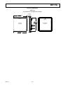
Figure 3. Basic System Configuration
RESERVED
RESERVED
Program Memory Interface
2K 3 24
EXTERNAL
The on-chip program memory address bus (PMA) and on-chip
program memory data bus (PMD) are multiplexed with the onchip data memory buses (DMA, DMD), creating a single external data bus and a single external address bus. The external
data bus is bidirectional and is 24 bits wide to allow instruction
fetches from external program memory. Program memory may
contain code and data.
0x37FF
0x3800
0x3FFF
MMAP = 0
2K 3 24
INTERNAL
ROM
0x37FF
0x3800
0x3FFF
MMAP = 1
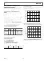
Figure 4. ADSP-2165/ADSP-2166 Program Memory Maps
ADSP-2161/ADSP-2162
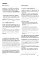
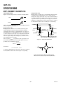
When MMAP = 0, on-chip program memory ROM occupies
8K words beginning at address 0x0000. Off-chip program
memory uses the remaining 8K words beginning at address
0x2000.
The external address bus is 14 bits wide. For the ADSP-216x,
these lines can directly address up to 16K words, of which 2K
are on-chip.
When MMAP = 1, 2K words of off-chip program memory begin
at address 0x0000. 6K words of on-chip program memory ROM
are at 0x0800 to 0x1FF0, and the remainder 2K words of program memory ROM is at 0x3800 to 0x3FFF. An additional 6K
of off-chip program memory is at 0x2000 to 0x37FF.
The data lines are bidirectional. The program memory select
(PMS) signal indicates accesses to program memory and can be
used as a chip select signal. The write (WR) signal indicates a
write operation and is used as a write strobe. The read (RD)
signal indicates a read operation and is used as a read strobe or
output enable signal.
0x0000
0x0000
2K
EXTERNAL
The ADSP-216x processors write data from their 16-bit registers to 24-bit program memory using the PX register to provide
the lower eight bits. When the processor reads 16-bit data from
24-bit program memory to a 16-bit data register, the lower eight
bits are placed in the PX register.
0x7FFF
0x0800
8K
INTERNAL
ROM
6K
INTERNAL
ROM
0x1FF0
0x1FF0
RESERVED
The program memory interface can generate 0 to 7 wait states for
external memory devices; default is to 7 wait states after RESET.
RESERVED
0x1FFF
0x2000
0x1FFF
0x2000
Program Memory Maps
6K
EXTERNAL
8K
EXTERNAL
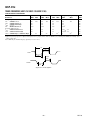
Program memory can be mapped in two ways, depending on the
state of the MMAP pin. Figure 4 shows the program memory
map for the ADSP-2165/ADSP-2166. Figures 5 and 6 show the
program memory maps for the ADSP-2161/ADSP-2162 and
ADSP-2163/ADSP-2164, respectively.
0x3FFF
MMAP = 0
2K
INTERNAL
ROM
0x37FF
0x3800
0x3FFF
MMAP = 1
Figure 5. ADSP-2161/ADSP-2162 Program Memory Maps
REV. 0
–7–