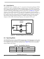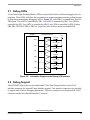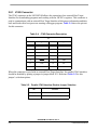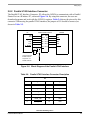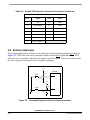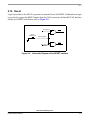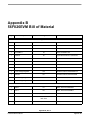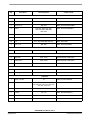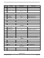
1
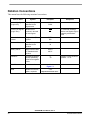
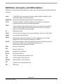
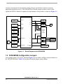
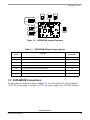
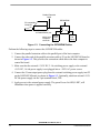
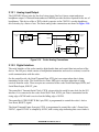
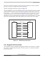
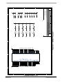
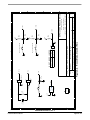
56F826
Evaluation Module User Manual
56F800
16-bit Digital Signal Controllers
DSP56F826EVMUM
Rev. 2
07/2005
freescale.com
TABLE OF CONTENTS
Preface vii
Audience . . . . . . . . . . . . . . . . . . . . . . . . . . . . . . . . . . . . . . . . . . . . . . . . . . . . . . . vii
Organization . . . . . . . . . . . . . . . . . . . . . . . . . . . . . . . . . . . . . . . . . . . . . . . . . . . . . vii
Suggested Reading . . . . . . . . . . . . . . . . . . . . . . . . . . . . . . . . . . . . . . . . . . . . . . . . vii
Notation Conventions . . . . . . . . . . . . . . . . . . . . . . . . . . . . . . . . . . . . . . . . . . . . . . viii
Definitions, Acronyms, and Abbreviations . . . . . . . . . . . . . . . . . . . . . . . . . . . . . . ix
References . . . . . . . . . . . . . . . . . . . . . . . . . . . . . . . . . . . . . . . . . . . . . . . . . . . . . . . x
Chapter 1
Introduction
1.1
1.2
1.3
56F826EVM Architecture. . . . . . . . . . . . . . . . . . . . . . . . . . . . . . . . . . . . . . . . . . . . . . . . 1-1
56F826EVM Configuration Jumpers . . . . . . . . . . . . . . . . . . . . . . . . . . . . . . . . . . . . . . . 1-2
56F826EVM Connections. . . . . . . . . . . . . . . . . . . . . . . . . . . . . . . . . . . . . . . . . . . . . . . . 1-3
Chapter 2
Technical Summary
2.1
56F826. . . . . . . . . . . . . . . . . . . . . . . . . . . . . . . . . . . . . . . . . . . . . . . . . . . . . . . . . . . . . . . 2-2
2.2
Program and Data Memory . . . . . . . . . . . . . . . . . . . . . . . . . . . . . . . . . . . . . . . . . . . . . . . 2-3
2.3
SPI EEPROM Memory . . . . . . . . . . . . . . . . . . . . . . . . . . . . . . . . . . . . . . . . . . . . . . . . . . 2-4
2.4
RS-232 Serial Communications . . . . . . . . . . . . . . . . . . . . . . . . . . . . . . . . . . . . . . . . . . . 2-5
2.5
Clock Source . . . . . . . . . . . . . . . . . . . . . . . . . . . . . . . . . . . . . . . . . . . . . . . . . . . . . . . . . . 2-6
2.6
Operating Mode . . . . . . . . . . . . . . . . . . . . . . . . . . . . . . . . . . . . . . . . . . . . . . . . . . . . . . . 2-6
2.7
Debug LEDs . . . . . . . . . . . . . . . . . . . . . . . . . . . . . . . . . . . . . . . . . . . . . . . . . . . . . . . . . . 2-7
2.8
Debug Support . . . . . . . . . . . . . . . . . . . . . . . . . . . . . . . . . . . . . . . . . . . . . . . . . . . . . . . . 2-7
2.8.1
JTAG Connector . . . . . . . . . . . . . . . . . . . . . . . . . . . . . . . . . . . . . . . . . . . . . . . . . . . . 2-8
2.8.2
Parallel JTAG Interface Connector . . . . . . . . . . . . . . . . . . . . . . . . . . . . . . . . . . . . . . 2-9
2.9
External Interrupts. . . . . . . . . . . . . . . . . . . . . . . . . . . . . . . . . . . . . . . . . . . . . . . . . . . . . 2-10
2.10 Reset . . . . . . . . . . . . . . . . . . . . . . . . . . . . . . . . . . . . . . . . . . . . . . . . . . . . . . . . . . . . . . . 2-11
2.11 Power Supply . . . . . . . . . . . . . . . . . . . . . . . . . . . . . . . . . . . . . . . . . . . . . . . . . . . . . . . . 2-12
2.12 Stereo Codec . . . . . . . . . . . . . . . . . . . . . . . . . . . . . . . . . . . . . . . . . . . . . . . . . . . . . . . . . 2-13
2.12.1
Analog Input/Output . . . . . . . . . . . . . . . . . . . . . . . . . . . . . . . . . . . . . . . . . . . . . . . . 2-14
2.12.2
Digital Interface . . . . . . . . . . . . . . . . . . . . . . . . . . . . . . . . . . . . . . . . . . . . . . . . . . . . 2-14
2.13 Daughter Card Connectors . . . . . . . . . . . . . . . . . . . . . . . . . . . . . . . . . . . . . . . . . . . . . . 2-15
2.13.1
Memory Daughter Card Expansion Connector . . . . . . . . . . . . . . . . . . . . . . . . . . . . 2-16
2.13.2
Peripheral Daughter Card Expansion Connector. . . . . . . . . . . . . . . . . . . . . . . . . . . 2-17
2.14 Test Points. . . . . . . . . . . . . . . . . . . . . . . . . . . . . . . . . . . . . . . . . . . . . . . . . . . . . . . . . . . 2-18
Table of Contents, Rev. 2
Freescale Semiconductor
i
Appendix A
56F826EVM Schematics
Appendix B
56F826EVM Bill of Material
56F826EVM User Manual, Rev. 2
ii
Freescale Semiconductor
LIST OF FIGURES
1-1
Block Diagram of the 56F826EVM . . . . . . . . . . . . . . . . . . . . . . . . . . . . . . . . . . . . . 1-2
1-2
56F826EVM Jumper Reference . . . . . . . . . . . . . . . . . . . . . . . . . . . . . . . . . . . . . . . . 1-3
1-3
Connecting the 56F826EVM Cables . . . . . . . . . . . . . . . . . . . . . . . . . . . . . . . . . . . . . 1-4
2-1
Schematic Diagram of the External Memory Interface. . . . . . . . . . . . . . . . . . . . . . . 2-3
2-2
SPI EEPROM Memory Block Diagram . . . . . . . . . . . . . . . . . . . . . . . . . . . . . . . . . . 2-4
2-3
Schematic Diagram of the RS-232 Interface . . . . . . . . . . . . . . . . . . . . . . . . . . . . . . . 2-5
2-4
Schematic Diagram of the Clock Interface . . . . . . . . . . . . . . . . . . . . . . . . . . . . . . . . 2-6
2-5
Schematic Diagram of the Debug LED Interface . . . . . . . . . . . . . . . . . . . . . . . . . . . 2-7
2-6
Block Diagram of the Parallel JTAG Interface . . . . . . . . . . . . . . . . . . . . . . . . . . . . . 2-9
2-7
Schematic Diagram of the User Interrupt Interface. . . . . . . . . . . . . . . . . . . . . . . . . 2-10
2-8
Schematic Diagram of the RESET Interface . . . . . . . . . . . . . . . . . . . . . . . . . . . . . . 2-11
2-9
Schematic Diagram of the Power Supply . . . . . . . . . . . . . . . . . . . . . . . . . . . . . . . . 2-12
2-10
Codec Analog Connections . . . . . . . . . . . . . . . . . . . . . . . . . . . . . . . . . . . . . . . . . . . 2-14
2-11
CS4218 Stereo Audio Codec. . . . . . . . . . . . . . . . . . . . . . . . . . . . . . . . . . . . . . . . . . 2-15
A-1
56F826 Processor . . . . . . . . . . . . . . . . . . . . . . . . . . . . . . . . . . . . . . . . . . . . . . . . . A-2
A-2
RESET, MODE, CLOCK & IRQS . . . . . . . . . . . . . . . . . . . . . . . . . . . . . . . . . . . A-3
A-3
PROGRAM & DATA SRAM MEMORY . . . . . . . . . . . . . . . . . . . . . . . . . . . . . A-4
A-4
SPI Serial 1M-bit Serial EEPROM Memory . . . . . . . . . . . . . . . . . . . . . . . . . . . . A-5
A-5
SCI PORT, RS-232 and Connector . . . . . . . . . . . . . . . . . . . . . . . . . . . . . . . . . . . A-6
A-6
SSI 16-bit Stereo Codec . . . . . . . . . . . . . . . . . . . . . . . . . . . . . . . . . . . . . . . . . . . . A-7
A-7
Parallel JTAG Host Target Interface and JTAG Connector . . . . . . . . . . . . . . . . A-8
A-8
Daughter Card Expansion Connectors . . . . . . . . . . . . . . . . . . . . . . . . . . . . . . . . . A-9
A-9
Power Supplies. . . . . . . . . . . . . . . . . . . . . . . . . . . . . . . . . . . . . . . . . . . . . . . . . . A-10
A-10
Bypass Caps . . . . . . . . . . . . . . . . . . . . . . . . . . . . . . . . . . . . . . . . . . . . . . . . . . . . A-11
List of Figures, Rev. 2
Freescale Semiconductor
iii
56F826EVM User Manual, Rev. 2
iv
Freescale Semiconductor
LIST OF TABLES
1-1
56F826EVM Default Jumper Options . . . . . . . . . . . . . . . . . . . . . . . . . . . . . . . . . 1-3
2-1
SPI Port Connector Description . . . . . . . . . . . . . . . . . . . . . . . . . . . . . . . . . . . . . . 2-4
2-2
RS-232 Serial Connector Description . . . . . . . . . . . . . . . . . . . . . . . . . . . . . . . . . 2-5
2-3
Operating Mode Selection . . . . . . . . . . . . . . . . . . . . . . . . . . . . . . . . . . . . . . . . . . 2-6
2-4
JTAG Connector Description. . . . . . . . . . . . . . . . . . . . . . . . . . . . . . . . . . . . . . . . 2-8
2-5
Parallel JTAG Interface Disable Jumper Selection . . . . . . . . . . . . . . . . . . . . . . . 2-8
2-6
Parallel JTAG Interface Connector Description . . . . . . . . . . . . . . . . . . . . . . . . . 2-9
2-7
Codec Sample Rate Selector . . . . . . . . . . . . . . . . . . . . . . . . . . . . . . . . . . . . . . . 2-13
2-8
Memory Daughter Card Connector Description . . . . . . . . . . . . . . . . . . . . . . . . 2-16
2-9
Peripheral Daughter Card Connector Description . . . . . . . . . . . . . . . . . . . . . . . 2-17
List of Tables, Rev. 2
Freescale Semiconductor
v
56F826EVM User Manual, Rev. 2
vi
Freescale Semiconductor
Preface
This reference manual describes in detail the hardware on the 56F826 Evaluation Module.
Audience
This document is intended for application developers who are creating software for
devices using the Freescale 56F826 part.
Organization
This manual is organized into two chapters and two appendixes.
•
Chapter 1, Introduction - provides an overview of the 56F826EVM and its features.
•
Chapter 2, Technical Summary - describes the 56F826EVM hardware in detail.
•
Appendix A, 56F826EVM Schematics - contains the schematics of the
56F826EVM.
•
Appendix B, 56F826EVM Bill of Material - provides a list of the materials used on the
56F826EVM board.
Suggested Reading
More documentation on the 56F826 and the 56F826EVM kit may be found at URL:
http://www.freescale.com
Preface, Rev. 2
Freescale Semiconductor
vii
Notation Conventions
This manual uses the following notational conventions:
Term or Value
Symbol
Examples
Active High Signals
(Logic One)
No special symbol
attached to the signal name
A0
CLKO
Active Low Signals
(Logic Zero)
Noted with an
overbar in text and
in most figures
WE
OE
Hexadecimal Values
Begin with a “$” symbol
$0FF0
$80
Decimal Values
No special symbol
attached to the
number
10
34
Binary Values
Begin with the letter
“b” attached to the
number
b1010
b0011
Numbers
Considered positive
unless specifically
noted as a negative
value
5
-10
Blue Text
Linkable on-line
Bold
Reference sources,
paths, emphasis
Exceptions
In schematic drawings,
Active Low Signals may be
noted by a backslash:
/WE
Voltage is often shown as
positive: +3.3V
...refer to
Figure 1-1
...see:
http://www.freescale.com/...
56F826EVM User Manual, Rev. 2
viii
Freescale Semiconductor
Definitions, Acronyms, and Abbreviations
Definitions, acronyms and abbreviations for terms used in this document are defined below for
reference:
codec
COder/DECoder, a part used to convert analog signals to digital (Coder)
and digital signals to analog (Decoder)
EEPROM
Electrically Erasable Programmable Read-Only Memory
EVM
Evaluation Module, a hardware platform which allows a customer to
evaluate the silicon and develop their application
GPIO
General Purpose Input and Output Port; does not share pin functionality
with any other peripheral on the chip and can only be set as an input,
output or level-sensitive interrupt input
IC
Integrated Circuit
JTAG
Joint Test Action Group, a bus protocol/interface used for test and debug
LQFP
Low-profile Quad Flat Pack
MPIO
Multi-Purpose Input and Output Port; shares package pins with other
peripherals on the chip and can function as a GPIO
OnCETM
On-Chip Emulation, a debug bus and port created by Freescale to enable
designers to create a low-cost hardware interface for a
professional-quality debug environment
PCB
Printed Circuit Board
PLL
Phase Locked Loop
RAM
Random Access Memory
ROM
Read-Only Memory
SCI
Serial Communications Interface Port
SPI
Serial Peripheral Interface Port
SRAM
Static Random Access Memory
SSI
Synchronous Serial Interface Port
WS
Wait State
Preface, Rev. 2
Freescale Semiconductor
ix
References
The following sources were used to produce this manual:
[1] DSP56800 Family Manual, , DSP56800FM, Freescale Semiconductor
[2] 56F826/827 User’s Manual, DSP56F826-827UM, Freescale Semiconductor
[3] 56F826 Technical Data, DSP56F826, Freescale Semiconductor
56F826EVM User Manual, Rev. 2
x
Freescale Semiconductor
Chapter 1
Introduction
The 56F826EVM is used to demonstrate the abilities of the 56F826 and to provide a hardware
tool allowing the development of applications that use the 56F826.
The 56F826EVM is an evaluation module board that includes a 56F826 part, 16-bit stereo codec,
external memory and a daughter card expansion interface. The daughter card expansion
connectors are for signal monitoring and user feature expandability.
The 56F826EVM is designed for the following purposes:
•
Allowing new users to become familiar with the features of the 56800 architecture. The
tools and examples provided with the 56F826EVM facilitate evaluation of the feature set
and the benefits of the family.
•
Serving as a platform for real-time software development. The tool suite enables the user
to develop and simulate routines, download the software to on-chip or on-board RAM, run
it, and debug it using a debugger via the JTAG/OnCETM port. The breakpoint features of
the OnCE port enable the user to easily specify complex break conditions and to execute
user-developed software at full-speed, until the break conditions are satisfied. The ability
to examine and modify all user accessible registers, memory and peripherals through the
OnCE port greatly facilitates the task of the developer.
•
Serving as a platform for hardware development. The hardware platform enables the user
to connect external hardware peripherals. The on-board peripherals can be disabled,
allowing the user to reassign any and all of the hybrid controller's peripherals. The OnCE
port's unobtrusive design means that all of the memory on the board and on the chip are
available to the user.
1.1 56F826EVM Architecture
The 56F826EVM facilitates the evaluation of various features present in the 56F826 part. The
56F826EVM can be used to develop real-time software and hardware products based on the
56F826. The 56F826EVM provides the features necessary for a user to write and debug
Introduction, Rev. 2
Freescale Semiconductor
1-1
software, demonstrate the functionality of that software and interface with the customer's
application-specific device(s). The 56F826EVM is flexible enough to allow a user to fully
exploit the 56F826's features to optimize the performance of his product, as shown in Figure 1-1.
56F826
RESET
LOGIC
MODE
LOGIC
Program Memory
64Kx16-bit
SRAM
RESET
MODE
SPI
SPI EEPROM
1M-bit
IRQ
IRQ Interface
SCI
RS-232
Interface
DSub
9-Pin
Address,
Data &
Control
Peripheral
Daughter
Card
Connector
Data Memory
64Kx16-bit
SRAM
Memory
Daughter Card
Connector
JTAG
Connector
DSub
25-Pin
JTAG/OnCE
Parallel
JTAG
Interface
4.00MHz
Crystal
SSI
GPIO
XTAL/EXTAL
+2.5V, +3.3V
& GND
Stereo Line In
Stereo 16-bit
Codec
Stereo Line Out
Amp
Headphone Jack
Debug LEDs
Power Supply
+2.5V, +3.3V & +5.0V
Figure 1-1. Block Diagram of the 56F826EVM
1.2 56F826EVM Configuration Jumpers
Seven jumper groups, (JG1-JG7), shown in Figure 1-2, are used to configure various features on
the 56F826EVM board. Table 1-1 describes the default jumper group settings.
56F826EVM User Manual, Rev. 2
1-2
Freescale Semiconductor 56F826EVM Connections
JG1
JG2
2
8
1
7
JG3
JG7
TB1
JG2
P3
P2
S1
JG1
JG5
JG5
Y1
JG3
JG4
J2
1
1
J3
S/N
3
P1
JTAG
RESET
JG7
JG6
U1
3
S2
U2
HEADPHONE
IRQA
S3
DSP56F826EVM
JG6
P6
J1
LEDS
IRQB
JG4
U5
P4
S4
U7
LINE
IN
P5
LINE
OUT
Figure 1-2. 56F826EVM Jumper Reference
Table 1-1. 56F826EVM Default Jumper Options
Jumper
Group
Comment
Jumpers
Connections
JG1
Enable on-board Parallel JTAG Host/Target Interface
NC
JG2
Enable RS-232 output
NC
JG3
Enable on-board SRAM
1–2
JG4
Use on-board EXTAL crystal input for oscillator
2–3
JG5
Use on-board XTAL crystal input for oscillator
1–2
JG6
Selects device’s Mode 0 operation upon exit from reset
1-2
JG7
Enable SPI EEPROM
1–2, 3–4, 5–6 & 7–8
1.3 56F826EVM Connections
An interconnection diagram is shown in Figure 1-3 for connecting the PC and the external
+12.0V DC power supply or external +5.0V DC lab power supply to the 56F826EVM board.
Introduction, Rev. 2
Freescale Semiconductor
1-3
Parallel Extension
Cable
56F826EVM
PC-compatible
Computer
P1
Connect cable
to Parallel/Printer port
P2
External
with 2.1mm, +12.0V
receptacle
Power
connector
TB1
+5.0V
Lab
Supply
Figure 1-3. Connecting the 56F826EVM Cables
Perform the following steps to connect the 56F826EVM cables:
1. Connect the parallel extension cable to the parallel port of the host computer
2. Connect the other end of the parallel extension cable to P1 on the 56F826EVM board as
shown in Figure 1-3. This provides the connection which allows the host computer to
control the board.
3. Make sure that the external +12.0V DC, 2.1A switching power supply or the external
+5.0V DC, 1A lab power supply is not plugged into a +120V AC power source
4. Connect the 2.1mm output power plug from the external switching power supply into P2
on the 56F826EVM board, as shown in Figure 1-3. Optionally, attach an external +5.0V
DC lab power supply via the 2-pin terminal block, TB1.
5. Apply power to the external power supply. The green Power-On LED, LED7, will
illuminate when power is applied correctly.
56F826EVM User Manual, Rev. 2
1-4
Freescale Semiconductor Chapter 2
Technical Summary
The 56F826EVM is designed as a versatile controller development card for developing
real-time software and hardware products to support a new generation of applications in
digital and wireless messaging, digital answering machines, feature phones, modems, and
digital cameras. The power of the 16-bit 56F826 device, combined with the on-board
64K u16-bit external program static RAM (SRAM), 64K u16-bit external data SRAM,
RS-232 interface, stereo 16-bit codec interface, Daughter Card Expansion interface and
parallel JTAG interface, makes the 56F826EVM ideal for developing and implementing
many audio and voice algorithms, as well as for learning the architecture and instruction
set of the 56F826 processor.
The main features of the 56F826EVM, with board and schematic reference designators,
include:
•
56F826EVM 16-bit +2.5V/+3.3V controller operating at 80MHz [U1]
•
External fast static RAM (FSRAM) memory [U2], configured as:
— 64Ku16 bits of Program memory with 0 wait states at 70MHz
— 64Ku16 bits of Data memory with 0 wait states at 70MHz
•
1Mbit Serial EEPROM [U4]
•
4.00MHz crystal oscillator for device frequency generation [Y1]
•
Optional external oscillator frequency input connector [JG4 and JG5]
•
Joint Test Action Group (JTAG) port interface connector for an external debug
Host Target Interface [J3]
•
On-board Parallel JTAG Host Target Interface, with a connector for a PC printer
port cable [P2]
•
RS-232 interface for easy connection to a host processor [U3 and P3]
•
16-bit stereo codec interface [U5, P4 and P5]
•
Stereo headphone interface [U6 and P6]
Technical Summary, Rev. 2
Freescale Semiconductor
2-1
•
Codec sample rate selector [S4]
•
Peripheral Daughter Card Expansion Connector, to allow the user to connect his own SCI,
SSI, SPI or GPIO-compatible peripheral to the controller[J2]
•
Memory Daughter Card Expansion Connector, to allow the user to connect his own
memory or memory device to the controller[J1]
•
On-board power regulation from an external +12V DC-supplied power input [P1]
•
On-board power regulation from an optional +5V DC-supplied power input [TB1]
•
Light Emitting Diode (LED) power indicator [LED7]
•
Six on-board real-time user debugging LEDs [LED1-6]
•
Manual RESET push-button [S1]
•
Manual interrupt push-button for IRQA [S2]
•
Manual interrupt push-button for IRQB [S3]
2.1 56F826
The 56F826EVM uses a Freescale DSP56F826BU80 part, designated as U1 on the board and in
the schematics. This part will operate at a maximum speed of 80MHz. A full description of the
56F826, including functionality and user information, is provided in these documents:
•
56F826 Preliminary Technical Data Sheet, (DSP56F826-827 UM): Provides features list
and specifications including signal descriptions, DC power requirements, AC timing
requirements and available packaging.
•
56F826/827 16-Bit Digital Signal Processor User’s Manual, (56F826UM): Provides an
overview description of the and detailed information about the on-chip components
including the memory and I/O maps, peripheral functionality, and control/status register
descriptions for each subsystem.
•
DSP56F800Family Manual, (DSP56F800FM): Provides a detailed description of the core
processor, including internal status and control registers and a detailed description of the
family instruction set.
Refer to these documents for detailed information about chip functionality and operation. They
can be found on this URL:
http://www.freescale.com
56F826EVM User Manual, Rev. 2
2-2
Freescale Semiconductor Program and Data Memory
2.2 Program and Data Memory
The 56F826EVM uses one bank of 128Ku16-bit Fast Static RAM (GSI GS72116, labeled U2)
for external memory expansion; see the FSRAM schematic diagram in Figure 2-1. This physical
memory bank is split into two logical memory banks of 64Kx16-bits: one for Program memory
and the other for Data memory. By using the controller’s program strobe, PS, signal line along
with the memory chip’s A0 signal line, half of the memory chip is selected when program
memory accesses are requested and the other half of the memory chip is selected when data
memory access are requested. This memory bank will operate with zero wait state accesses while
the 56F826 is running at 70MHz. However, when running at 80MHz, the memory bank operates
with four wait state accesses. This memory bank can be disabled by removing the jumper at JG3.
GS72116
56F826
A0-A15
A1-A16
A0
PS
D0-D15
DQ0-DQ15
RD
OE
WR
WE
+3.3V
Jumper Removed:
Disable SRAM
JG3
1
2
Jumper Pin 1-2:
Enable SRAM
CE
Figure 2-1. Schematic Diagram of the External Memory Interface
Technical Summary, Rev. 2
Freescale Semiconductor
2-3
2.3 SPI EEPROM Memory
A 1Mbit, +3.3V, SPI, serial EEPROM Memory, Atmel AT45DB011-SC, is provided on the
56F826EVM; reference Figure 2-2. This memory connects directly to the SPI Port through a
header on the 56F826. It can be used to load program code and data into the 56F826’s internal or
external memory spaces. A jumper block, JG7, is provided, which allows the user to disconnect
the on-board SPI EEPROM from the SPI port and to connect his own SPI port peripheral. The
header details are shown in Table 2-1.
EEPROM Enable
JG7
56F826
Serial EEPROM
MOSI
SDI
MISO
SDO
SCLK
SCK
GPIOF7
CS
(SPI Port Connector)
Figure 2-2. SPI EEPROM Memory Block Diagram
Table 2-1. SPI Port Connector Description
JG7
Pin #
Signal
Pin #
Signal
1
SS/GPIO7
2
CS
3
MISO
4
SDO
5
MOSI
6
SDI
7
SCLK
8
SCK
56F826EVM User Manual, Rev. 2
2-4
Freescale Semiconductor RS-232 Serial Communications
2.4 RS-232 Serial Communications
The 56F826EVM provides an RS-232 interface by the use of an RS-232 level converter, (Maxim
MAX3245EEAI, designated as U3). Refer to the RS-232 schematic diagram in Figure 2-3. The
RS-232 level converter transitions the SCI UART’s +3.3V signal levels to RS-232 compatible
signal levels and connects to the host’s serial port via connector P3. Flow control is not provided,
but could be implemented using uncommitted GPIO signals. The pinout of connector P3 is listed
in Table 2-2. The RS-232 level converter/transceiver can be disabled by placing a jumper at JG2.
RS-232
Level Converter
Interface
56F826
P3
TXDO
T1in
RXDO
R1out
T1out
R1in
+3.3V
x
FORCEOFF
Jumper Removed:
Enable RS-232
Jumper Pin 1-2:
Disable RS-232
1
6
2
7
3
8
4
9
5
JG2
1
2
Figure 2-3. Schematic Diagram of the RS-232 Interface
Table 2-2. RS-232 Serial Connector Description
P3
Pin #
Signal
Pin #
Signal
1
Jumper to 6 & 4
6
Jumper to 1 & 4
2
TXD
7
Jumper to 8
3
RXD
8
Jumper to 7
4
Jumper to 1 & 6
9
N/C
5
GND
Technical Summary, Rev. 2
Freescale Semiconductor
2-5
2.5 Clock Source
The 56F826EVM uses a 4.00MHz crystal, Y1, connected to its External Crystal Inputs, EXTAL
and XTAL. To achieve its 80MHz maximum operating frequency, the 56F826 uses its internal
PLL to multiply the input frequency by 20. An external oscillator source can be connected to the
controller by using the oscillator bypass connectors, JG4 and JG5; see Figure 2-4. If the input
frequency is above 4MHz, then the EXTAL input should be jumpered to ground by adding a
jumper between JG4 pins 2 and 3. The input frequency would then be injected on JG5’s pin 2. If
the controller needs to be synchronized to the codec’s sample frequency, then the controller’s
input frequency should be jumpered using the 12.2280MHz codec frequency. If the input
frequency is below 4MHz, then the input frequency can be injected on JG4’s pin 2.
EXTERNAL
OSCILLATOR
HEADERS
56F826
JG4
3
2
EXTAL
1
4.00MHz
10M
JG5
1
2
12.2880MHz
3
XTAL
Figure 2-4. Schematic Diagram of the Clock Interface
2.6 Operating Mode
The 56F826EVM provides a boot-up MODE selection jumper, JG6. This jumper is used to select
the operating mode of the controller as it exits RESET. Refer to the DSP56F826 User’s Manual
for a complete description of the chip’s operating modes. Table 2-3 shows the two operating
modes available on the 56F826.
Table 2-3. Operating Mode Selection
Operating Mode
JG6
Comment
0
1–2
Bootstrap from internal memory
3
No Jumper
Bootstrap from external memory
56F826EVM User Manual, Rev. 2
2-6
Freescale Semiconductor Debug Support
2.7 Debug LEDs
Six on-board Light-Emitting Diodes (LEDs) are provided to allow real-time debugging for user
programs. These LEDs will allow the programmer to monitor program execution without having
to stop the program during debugging; refer to Figure 2-5. User LED1 is controlled by Port B’s
PB0 signal. User LED2 is controlled by PB1. User LED3 is controlled by PB2. User LED4 is
controlled by PB3. User LED5 is controlled by PB4. User LED6 is controlled by PB5. Setting
PB0, PB1, PB2, PB3, PB4 or PB5 to a Logic One value will turn on the associated LED.
56F826
INVERTING BUFFER
+3.3V
RED LED
PB0
YELLOW LED
PB1
GREEN LED
PB2
RED LED
PB3
YELLOW LED
PB4
GREEN LED
PB5
Figure 2-5. Schematic Diagram of the Debug LED Interface
2.8 Debug Support
The 56F826EVM provides an on-board Parallel JTAG Host Target Interface and a JTAG
interface connector for external Target Interface support. Two interface connectors are provided
to support each of these debugging approaches. These two connectors are designated the JTAG
connector and the Host Parallel Interface Connector.
Technical Summary, Rev. 2
Freescale Semiconductor
2-7
2.8.1 JTAG Connector
The JTAG connector on the 56F826EVM allows the connection of an external Host Target
Interface for downloading programs and working with the 56F826’s registers. This connector is
used to communicate with an external Host Target Interface which passes information and data
back and forth with a host processor running a debugger program. Table 2-4 shows the pin-out
for this connector.
Table 2-4. JTAG Connector Description
J3
Pin #
Signal
Pin #
Signal
1
TDI
2
GND
3
TDO
4
GND
5
TCK
6
GND
7
NC
8
KEY
9
RESET
10
TMS
11
+3.3V
12
NC
13
NC
14
TRST
When this connector is used with an external Host Target Interface, the parallel JTAG interface
should be disabled by placing a jumper in jumper block JG1. Reference Table 2-5 for this
jumper’s selection options.
Table 2-5. Parallel JTAG Interface Disable Jumper Selection
JG1
Comment
No jumpers
On-board Parallel JTAG Interface Enabled
1–2
Disable on-board Parallel JTAG Interface
56F826EVM User Manual, Rev. 2
2-8
Freescale Semiconductor Debug Support
2.8.2 Parallel JTAG Interface Connector
The Parallel JTAG Interface Connector, P2, allows the 56F826 to communicate with a Parallel
Printer Port on a Windows PC; reference Figure 2-6. By using this connector, the user can
download programs and work with the 56F826’s registers. Table 2-6 shows the pin-out for this
connector. When using the parallel JTAG interface, the jumper at JG1 should be removed, as
shown in Table 2-5.
Parallel JTAG Interface
P2
IN OUT
OUT IN
TDI
TDO
P_TRST
OUT
TDI
TDO
TRST
IN
OUT
TMS
IN
OUT
TCK
OUT
RESET
IN
TMS
TCK
IN
P_RESET
+3.3V
JG1
DB-25 Connector
56F826
EN
1
2
Jumper Removed:
Enable JTAG I/F
Jumper Pin 1-2:
Disable JTAG I/F
Figure 2-6. Block Diagram of the Parallel JTAG Interface
Table 2-6. Parallel JTAG Interface Connector Description
P2
Pin #
Signal
Pin #
Signal
1
NC
14
NC
2
PORT_RESET
15
PORT_IDENT
3
PORT_TMS
16
NC
4
PORT_TCK
17
NC
5
PORT_TDI
18
GND
6
PORT_TRST
19
GND
Technical Summary, Rev. 2
Freescale Semiconductor
2-9
Table 2-6. Parallel JTAG Interface Connector Description (Continued)
P2
Pin #
Signal
Pin #
Signal
7
NC
20
GND
8
PORT_IDENT
21
GND
9
PORT_VCC
22
GND
10
NC
23
GND
11
PORT_TDO
24
GND
12
NC
25
GND
13
PORT_CONNECT
2.9 External Interrupts
Two on-board push-button switches are provided for external interrupt generation, as shown in
Figure 2-7. SW2 allows the user to generate a hardware interrupt for signal line IRQA. SW3
allows the user to generate a hardware interrupt for signal line IRQB. These two switches allow
the user to generate interrupts for his user-specific programs.
+3.3V
56F826
10K
SW2
IRQA
0.1µF
+3.3V
10K
SW3
IRQB
0.1µF
Figure 2-7. Schematic Diagram of the User Interrupt Interface
56F826EVM User Manual, Rev. 2
2-10
Freescale Semiconductor Reset
2.10 Reset
Logic is provided on the 56F826 to generate an internal Power-On RESET. Additional reset logic
is provided to support the RESET signals from the JTAG connector, the Parallel JTAG Interface
and the user RESET push-button; refer to Figure 2-8.
JTAG_RESET
RESET
RESET
PUSHBUTTON
MANUAL RESET
TRST
JTAG_TAP_RESET
Figure 2-8. Schematic Diagram of the RESET Interface
Technical Summary, Rev. 2
Freescale Semiconductor
2-11
2.11 Power Supply
The main power input, +12.0V DC, to the 56F826EVM is through a 2.1mm coax power jack. An
optional +5.0V DC power supply input is available through a 2-pin terminal block, TB1. A 1.2A
power supply is provided with the 56F826EVM; however, less than 500mA is required by the
EVM. The remaining current is available for the user’s custom daughter card application, when
connected to the daughter card interface. The power regulation on the 56F826EVM provides
+5.0V DC voltage regulation for the codec’s analog circuits and to the additonal voltage
regulation logic on the EVM. The additional voltage regulation logic provides +2.5V DC voltage
regulation for the controller’s core and +3.3V DC voltage regulation for the controller’s I/O,
memory, parallel JTAG interface and supporting logic; refer to Figure 2-9. Power applied to the
56F826EVM is indicated with a Power-On LED, referenced as LED7.
P1
+5.0V
Regulator
+12.0V DC
Power
Condition
+5.0V DC
Analog
+3.3V
Regulator
+3.3 VDC
CODEC
TB1
+5.0V DC
56F826
GND
56F826EVM
PARTS
+2.5V
Regulator
+2.5V DC
56F826
CORE
Figure 2-9. Schematic Diagram of the Power Supply
56F826EVM User Manual, Rev. 2
2-12
Freescale Semiconductor Stereo Codec
2.12 Stereo Codec
A 16-bit audio quality stereo codec, Crystal Semiconductor CS4218, is connected to the
56F826’s SSI port to support audio, voice and signal analysis applications. The codec is clocked
with a 12.288MHz oscillator, allowing the codec to operate between a sample frequency of 8kHz
and 48kHz. The sample rate can be manually set using the appropriate switch positions on dip
switch S4. This three position dip switch makes the sample rate selections detailed in Table 2-7
possible. The codec supports +3.3V digital levels, eliminating the need for voltage level
translation circuitry. Additionally, a set of zero ohm resistors are provided on the EVM to allow a
user to disconnect the on-board codec from the SSI port and to connect his own codec to the SSI
port; see Figure 2-11. The on-board codec has analog signal-conditioning logic, allowing direct
connection to its line level input and line level output signals through two 1/8” stereo jacks;
reference Figure 2-10.
Table 2-7. Codec Sample Rate Selector
SW 4
Position 3
(MF6)
SW 4
Position 2
(MF7)
SW 4
Position 3
(MF8)
Sample Rate
ON
ON
ON
48.00kHz
ON
ON
OFF
32.00kHz
ON
OFF
ON
24.00kHz
ON
OFF
OFF
19.20kHz
OFF
ON
ON
16.00kHz
OFF
ON
OFF
12.00kHz
OFF
OFF
ON
9.60kHz
OFF
OFF
OFF
8.00kHz
Technical Summary, Rev. 2
Freescale Semiconductor
2-13
2.12.1 Analog Input/Output
The 56F826EVM uses jacks for line level stereo input, line level stereo output and stereo
headphone output. A National Semiconductor LM4880 provides the drive required for the use of
headphones. This device offers a THD, which is superior to the CS4218’s on-chip headphone
drive circuitry by a factor of two. The basic analog codec connections are shown in Figure 2-10.
CS4218
P5
P4
Line Level
Input
RIN1
LOUTL
LIN1
LOUTR
Line Level
Output
A
A
LM4880
P6
Headphone
Output
A
Figure 2-10. Codec Analog Connections
2.12.2 Digital Interface
The serial interface of the codec transfers digital audio data and control data into and out of the
device. The SSI port, which consists of independent transmitter and receiver sections, is used for
serial communication with the codec.
On the controller side, the Serial Transmit Data, STD, pin is an output when data is being
transmitted to the codec. The Serial Receive Data, SRD, pin is an input when data is being
received from the codec. These two pins are connected to the codec Serial Data Input, SDIN, and
Serial Data Output, SDOUT, pins.
The controller’s Transmit Serial Clock, STCK, pin provides the serial bit rate clock for the SSI
interface. It is connected to the codec Serial Port Clock, SCLK, pin. Data is transmitted on the
rising edge of SCLK and is received on the falling edge of SCLK.
The controller’s GPIO PORT D Bit 0 pin, PD0, is programmed to control the codec’s Active
Low Reset, RESET, signal.
The Serial Transmit Frame Sync pin, STFS, is programmed to control the codec’s Frame Sync,
FSYNC, signal. FSYNC is sampled by SCLK, with a rising edge indicating that a new frame is
56F826EVM User Manual, Rev. 2
2-14
Freescale Semiconductor Daughter Card Connectors
about to start. The FSYNC frequency is always the system’s sample rate. It may be an input to
the codec, or it may be an output from the codec in data mode.
The basic codec digital connections are shown in Figure 2-11.
The codec’s MODE is set by the three MODE selection resistors, R96-R98. In the factory default
setting of MODE 4, the codec is set to be the Master of the SPI bus with its data word set at 32
bits per frame; i.e., 16 bits, Left channel and 16 bits, Right channel. The sample rate is selected
on Sample Rate Selector switch S4; reference Table 2-7 for selection options. Codec control
information is sent over a separate serial port using: PD1 as the Control Chip Select, CCS, signal;
PD2 as the Control Data Input, CDIN, signal; and PD3 as the Control Clock, CCLK, signal.
56F826
CODEC Enable Logic
CS4218
STD
SDIN
SRD
SDOUT
STCK
SCLK
STFS
FSYNC
PD0
RESET
PD1
CCS
PD2
CDIN
PD3
CCLK
Figure 2-11. CS4218 Stereo Audio Codec
2.13 Daughter Card Connectors
The EVM board contains two daughter card expansion connectors. One connector, J1, contains
the controller’s external memory bus signals. The other connector, J2, contains the controller’s
peripheral port signals.
Technical Summary, Rev. 2
Freescale Semiconductor
2-15
2.13.1 Memory Daughter Card Expansion Connector
The controller’s external memory bus signals are connected to the Memory Daughter Card
Expansion connector, J1. Table 2-8 shows the port signal to pin assignments.
Table 2-8. Memory Daughter Card Connector Description
J1
Pin #
Signal
Pin #
Signal
1
A10
2
A11
3
A9
4
DS
5
A8
6
A15
7
A7
8
A14
9
GND
10
GND
11
WR
12
A13
13
D0
14
A12
15
D1
16
D8
17
D2
18
D9
19
GND
20
GND
21
D3
22
D10
23
D4
24
D11
25
D5
26
D12
27
D6
28
D13
29
GND
30
GND
31
D7
32
D14
33
PS
34
D15
35
A0
36
RD
37
A1
38
A6
39
GND
40
GND
41
A2
42
A5
56F826EVM User Manual, Rev. 2
2-16
Freescale Semiconductor Daughter Card Connectors
Table 2-8. Memory Daughter Card Connector Description (Continued)
J1
Pin #
Signal
Pin #
Signal
43
A3
44
A4
45
GND
46
GND
47
+3.3V
48
+3.3V
49
GND
50
GND
51
GND
2.13.2 Peripheral Daughter Card Expansion Connector
The controller’s peripheral port signals are connected to the Peripheral Daughter Card Expansion
connector, J2. Table 2-9 shows the port signal to pin assignments.
Table 2-9. Peripheral Daughter Card Connector Description
J2
Pin #
Signal
Pin #
Signal
1
PB0
2
PB1
3
CLKO
4
PB2
5
TA0
6
TA1
7
PB3
8
PB4
9
TA2
10
TA3
11
PB5
12
PB6
13
GND
14
GND
15
SRD
16
PB7
17
SRFS
18
PD0
19
SCLK
20
PD1
21
GND
22
GND
23
MOSI
24
PD2
Technical Summary, Rev. 2
Freescale Semiconductor
2-17
Table 2-9. Peripheral Daughter Card Connector Description (Continued)
J2
Pin #
Signal
Pin #
Signal
25
MISO
26
PD3
27
GND
28
GND
29
SS
30
PD4
31
SRCK
32
PD5
33
STFS
34
PD6
35
RESET
36
PD7
37
GND
38
GND
39
STD
40
RXD1
41
STCK
42
TXD1
43
IRQB
44
RXD0
45
IRQA
46
TXD0
47
+3.3V
48
+3.3V
49
GND
50
GND
51
GND
2.14 Test Points
The 56F826EVM board has a total of seven test points. Three digital GND test points are located
in corners of the board. The +5.0VA and AGND test points are located in the analog corner of the
board. The +2.5V and +3.3V test points are located in the power supply section of the board.
56F826EVM User Manual, Rev. 2
2-18
Freescale Semiconductor Appendix A
56F826EVM Schematics
56F826EVM Schematics, Rev. 2
Freescale Semiconductor
Appendix A-1
56F826EVM User Manual, Rev. 2
Appendix A-2
Freescale Semiconductor 1
2
3
4
TXD1
RXD1
TXD0
RXD0
MISO
MOSI
SCLK
/SS
A
TDI
TDO
TCK
TMS
/TRST
/DE
TCS
TA0
TA1
TA2
TA3
XBOOT
/RESET
SRD
STD
STFS
SRFS
STCK
SRCK
D[0..15]
A
D0
D1
D2
D3
D4
D5
D6
D7
D8
D9
D10
D11
D12
D13
D14
D15
63
31
58
19
95
81
6
2
3
100
1
4
98
99
91
90
89
88
25
45
51
54
55
52
56
53
93
92
97
96
86
85
84
87
34
35
36
37
38
39
40
41
42
43
44
46
47
48
49
50
U1
GND1
GND2
GND3
GND4
GND5
GND6
GND7
TDI
TDO
TCK
TMS
TRST
DE
TCS
TA0/PF0
TA1/PF1
TA2/PF2
TA3/PF3
XBOOT
RESET
DSP56F826BU80
SRD/PC0
STD/PC3
STFS/PC4
SRFS/PC1
STCK/PC5
SRCK/PC2
TXD1/MISO0
RXD1/SS0
TXD0/SCLK0
RXD0/MOSI0
MISO/PF6
MOSI/PF5
SCLK/PF4
SS/PF7
D0
D1
D2
D3
D4
D5
D6
D7
D8
D9
D10
D11
D12
D13
D14
D15
B
VDD1
VDD2
VDD3
VDD4
VDDC1
VDDC2
VDDC3
VDDA
VSSA
IRQA
IRQB
CLKO
EXTAL
XTAL
WR
RD
PS
DS
PD0
PD1
PD2
PD3
PD4
PD5
PD6
PD7
PB0
PB1
PB2
PB3
PB4
PB5
PB6
PB7
A0/PE0
A1/PE1
A2/PE2
A3/PE3
A4/PE4
A5/PE5
A6/PE6
A7/PE7
A8/PA0
A9/PA1
A10/PA2
A11/PA3
A12/PA4
A13/PA5
A14/PA6
A15/PA7
B
5
30
57
80
94
64
20
59
60
32
33
65
61
62
27
26
29
28
74
75
76
77
78
79
82
83
66
67
68
69
70
71
72
73
24
23
22
21
18
17
16
15
14
13
12
11
10
9
8
7
A0
A1
A2
A3
A4
A5
A6
A7
A8
A9
A10
A11
A12
A13
A14
A15
C
PB5
PB4
PB3
PB2
PB1
PB0
B
Size
Title
13
11
9
5
3
1
2
4
6
8
10
12
GREEN LED
LED6
YELLOW LED
LED5
RED LED
LED4
GREEN LED
LED3
YELLOW LED
LED2
RED LED
LED1
D
270
R14
270
R13
270
R11
270
R9
270
R6
270
R3
+3.3V
DSP56F826EVM.DSN
D
Date: Sunday, April 08, 2001
Document
Number
47K
R12
47K
R10
47K
R8
47K
R7
47K
R5
47K
R4
R81
R80
R93
R92
R79
E
+3.3V
DNP
10K
DNP
10K
10K
10K
DNP
10K
E
of
10
1.2
Rev.
FAX: (480) 413-2510
Sheet 1
(480) 413-5090
2100 East Elliot Road
Tempe, Arizona 85284
DSP Standard Products Division
PB5
PB4
PB3
PB2
PB1
PB0
TDI
TCK
TCS
/DE
TMS
Designer: DSPD Design
DSP56F826 Processor and DEBUG LEDS
MC74AC04AD
U11F
MC74AC04AD
U11E
MC74AC04AD
U11D
MC74AC04AD
U11C
MC74AC04AD
U11B
MC74AC04AD
U11A
Figure A-1. 56F826 Processor
+2.5V
+3.3V
+2.5V
/IRQA
/IRQB
CLKO
EXTAL
XTAL
/WR
/RD
/PS
/DS
PD0
PD1
PD2
PD3
PD4
PD5
PD6
PD7
PB0
PB1
PB2
PB3
PB4
PB5
PB6
PB7
A[0..15]
C
1
2
3
4
56F826EVM Schematics, Rev. 2
Freescale Semiconductor
Appendix A-3
1
2
3
4
Y1
4.00MHz
A
A
S1
12.288MHZ
+3.3V
3
2
3
2
DS1818
1
RST
DS1818
DNP
GND
Vcc
U12
1
3
1
2
JG5
/POR
B
A
Size
Title
/POR
XTAL
EXTAL
DSP56F826EVM.DSN
C
Date: Sunday, April 08, 2001
Document
Number
RESET, CLOCK, BOOT MODE & IRQS
2
1
JG6
S3
D
D
XBOOT
/IRQB
/IRQA
E
E
of
10
1.2
Rev.
FAX: (480) 413-2510
S h eet 2
(480) 413-5090
2100 East Elliot Road
Tempe, Arizona 85284
DSP Standard Products Division
R72
10K
+2.5V
C31
0.1uF
R71
10K
+3.3V
C30
0.1uF
R70
10K
+3.3V
Designer: D S P D D e s i g n
IRQB PUSHBUTTON
S2
IRQA PUSHBUTTON
BOOT MODE JUMPER
EXT BOOT
NC
INT BOOT
1 - 2
C
Figure A-2. Reset, Mode, Clock & IRQs
C32
0.1uF
EXT OSC
>8MHZ
RESET PUSHBUTTON
10M
R1
2
OSC BYPASS
1
3
JG4
B
1
2
3
4
56F826EVM User Manual, Rev. 2
Appendix A-4
Freescale Semiconductor 1
2
3
4
NC
SRAM DISABLE
A
1-2
SRAM ENABLE
SRAM ENABLE JUMPER
OPTION
JG3
A
D
1
2
JG3
A
Size
Title
R68
1K
/RD
/WR
A0
A1
A2
A3
A4
A5
A6
A12
A13
A14
A15
A10
A9
A8
A7
A11
R69
1K
41
17
6
39
40
5
4
3
2
1
44
43
42
27
26
25
24
21
20
19
18
22
U2
VSS
VSS
VDD
VDD
DQ1
DQ2
DQ3
DQ4
DQ5
DQ6
DQ7
DQ8
DQ9
DQ10
DQ11
DQ12
DQ13
DQ14
DQ15
DQ16
G S 7 2 1 1 6 TP-12
OE
WE
CE
LB
UB
A0
A1
A2
A3
A4
A5
A6
A7
A8
A9
A10
A11
A12
A13
A14
A15
A16
DSP56F826EVM.DSN
C
Date: Sunday, April 08, 2001
Document
Number
P R O G R A M and DATA SRAM MEMORY
R67
10K
+3.3V
A[0..15]
/PS
D7
D6
D5
D4
D3
D2
D1
D0
D8
D9
D10
D11
D12
D13
D14
D15
+3.3V
D
E
E
of
10
1.2
Rev.
FAX: (480) 413-2510
S h eet 3
(480) 413-5090
2100 East Elliot Road
Tempe, Arizona 85284
DSP Standard Products Division
D[0..15]
Designer: D S P D D e s i g n
12
34
11
33
7
8
9
10
13
14
15
16
29
30
31
32
35
36
37
38
64Kx16-bit Program and 64Kx16-bit Data Memory
C
Figure A-3. Program & Data SRAM Memory
B
B
1
2
3
4
56F826EVM Schematics, Rev. 2
Freescale Semiconductor
Appendix A-5
1
2
3
4
A
A
5
MOSI
JG7
8
6
4
2
4
8
1
2
/EE_CS
EE_SO
EE_SI
EE_SCK
GND
WP
RESET
VCC
AT45DB011-SC
SCK
SI
SO
CS
U4
DSP56F826EVM.DSN
C
Date: Sunday, April 08, 2001
Document
Number
SPI Serial 1M-Bit EEPROM MEMO R Y
C
/WP
/RES
D
/WP
/RES
R91
R90
10K
10K
+3.3V
E
E
of
10
1.2
Rev.
FAX: (480) 413-2510
S h eet 4
(480) 413-5090
2100 East Elliot Road
Tempe, Arizona 85284
DSP Standard Products Division
Designer: D S P D D e s i g n
7
5
3
6
+3.3V
D
Figure A-4. SPI Serial 1M-bit Serial EEPROM Memory
A
Size
Title
EEPROM Enable
7
3
MISO
SCLK
1
/SS
B
B
1
2
3
4
56F826EVM User Manual, Rev. 2
Appendix A-6
Freescale Semiconductor 1
2
3
4
1 - 2
RS-232 DISABLE
A
N/C
RXD0
TXD0
RS-232 ENABLE
RS-232 ENABLE
A
1
2
JG2
R89
R88
A
Size
Title
/EN
1
1
1
1
1
T2IN
T3IN
22
23
20
19
18
17
16
15
14
13
12
2
24
1
28
U3
GND
V+
V-
VCC
INVALID
R1IN
R2IN
R3IN
R4IN
R5IN
T1OUT
T2OUT
T3OUT
21
4
5
6
7
8
9
10
11
1
T15
R2IN
R3IN
R4IN
R5IN
T8
T9
C28
1.0uF
27
25
C27
1.0uF
1
1
+3.3V
3
26
DSP56F826EVM.DSN
C
Date: Sunday, April 08, 2001
Document
Number
SCI PORT, RS-232 AND CONNECTOR
M A X 3 2 4 5EEAI
FORCEOFF
FORCEON
R2OUTB
R1OUT
R2OUT
R3OUT
R4OUT
R5OUT
T1IN
T2IN
T3IN
C2-
C1C2+
C1+
C
P3
DCD
DSR
TXD
CTS
RXD
RTS
DTR
RI
GND
D
R5IN
R4IN
R3IN
R2IN
T3IN
T2IN
/EN
E
R62
R61
R60
R59
R58
R56
R55
1K
1K
1K
1K
1K
1K
1K
+3.3V
E
of
10
1.2
Rev.
FAX: (480) 413-2510
S h eet 5
(480) 413-5090
2100 East Elliot Road
Tempe, Arizona 85284
DSP Standard Products Division
SCI
RS-232
CONNECTOR
1
6
2
7
3
8
4
9
5
Designer: D S P D D e s i g n
D
Figure A-5. SCI Port, RS-232 and Connector
B
T11
T12
T13
T14
T10
C29
1.0uF
C26
1.0uF
R57
1K
+3.3V
0 Ohm
0 Ohm
B
1
2
3
4
56F826EVM Schematics, Rev. 2
1
2
3
4
Line-Input
Stereo Jack
1/8"
P4
PD3
PD2
PD1
PD0
STFS
STCK
SRD
STD
3
11
10
2
1
R49
A
0 Ohm
R54
0 Ohm
R53
0 Ohm
R52
0 Ohm
R48
0 Ohm
R51
0 Ohm
R47
0 Ohm
R50
0 Ohm
+3.3V
TIP_IN
RING_IN
A
/CODEC_RESET
CODEC_FSYNC
CODEC_SCLK
CODEC_SDOUT
CCLK
CDIN
/CCS
GND
EN O U T
VCC
U7
5
12.288MHZ OSC
4
1
CODEC_SDIN
1K
R41
8
R32
5.62K
1%
R31
5.62K
1%
+3.3V
5.62K
1%
R33
5.62K
1%
R30
1K
R86
12.288MHZ
C12
470pF
C10
470pF
C14
0.33uF
C8
0.33uF
B
8.00
9.60
0
1
12.00
16.00
19.20
24.00
32.00
48.00
1
0
1
0
1
0
MF8
FS (KHZ)
5
3
1
R96
MODE3
MODE2
MODE1
GND
VDD
REFGND
REFBY
43
42
16
15
35
26
23
28
25
24
32
30
29
33
34
10
9
C9
0.1uF
C
LOUT
ROUT
+3.3V
MODE3
MODE2
MODE1
MF6
MF7
MF8
MF5
/CCS
CCLK
CDIN
MF1
LOUT
ROUT
C
+
1uF
25V
C19
1uF
25V
C20
C7
47uF
10VDC
C15
0.0022uF
C25
1uF
25V
20.0K
1%
R38
20.0K
1%
R39
B
Size
Title
5
3
2
6
GND
VDD
OUT_A
OUT_B
LM4880M
SHUTDN
BYPASS
IN_A
IN_B
U6
20.0K 1 %
R46
20.0K 1 %
R40
R34
39.2K
1%
D
4
8
1
7
+5.0VA
R35
39.2K
1%
TIP_OUT
RING_OUT
3
11
10
2
1
DSP56F826EVM.DSN
D
Date: Sunday, April 08, 2001
Document
Number
SSI 16-BIT STEREO CODEC
SHUTDN
BYPASS
C16
0.0022uF
C13
1uF
25V
C11
1uF
25V
Figure A-6. SSI 16-bit Stereo Codec
0 Ohm
DNP
R98
0 Ohm
R97
0 Ohm
WF6
WF7
WF8
MF5
MF4
MF3
MF2
MF1
LOUT
ROUT
SWODE3
SWODE2
SWODE1
CS4218-KQ
GNDA
VDDA
CLKIN
RESET
PDN
SSYNC
SCLK
SDOUT
SDIN
REFBUF
LIN2
RIN2
LIN1
RIN1
U5
SERIAL MODE 4 SELECTED
MASTER, 32BITS PER FRAME
1
1
1
0
1
1
0
0
S4
17
18
Sample Select
6
4
2
MF7
MF6
MF7
MF8
0
1
14
C21
0.47uF
+5.0VA
1
1
0
0
0
0
22
C18
0.47uF
41
40
7
39
38
37
36
20
21
19
C17
0.47uF
12.288MHZ
/CODEC_RESET
/PDN
CODEC_FSYNC
CODEC_SCLK
CODEC_SDOUT
CODEC_SDIN
MF6
B
+
+
Freescale Semiconductor
Appendix A-7
TIP_PHN
RING_PHN
1/8"
Headphone Out
Stereo Jack
P6
10K
10K
R37
10K
R36
10K
R45
10K
R44
10K
R43
10K
R85
10K
R84
10K
R83
MF1
10K
R42
10K
SHUTDN R87
MF5
/CCS
MF8
MF7
MF6
MODE3
MODE2
MODE1
/PDN
R82
+3.3V
E
of
10
1.2
Rev.
FAX: (480) 413-2510
Sheet 6
(480) 413-5090
2100 East Elliot Road
Tempe, Arizona 85284
DSP Standard Products Division
3
11
10
2
1
Designer: DSPD Design
C23
47uF
10VDC
C24
47uF
10VDC
1/8"
Line Out
Stereo Jack
P5
E
1
2
3
4
56F826EVM User Manual, Rev. 2
1
2
3
4
A
A
P_RESET
5.1K
R25
DB25M
13
12
11
10
9
8
7
6
5
4
3
2
1
B
Q1
2N2222A
/J_RESET
R24
5.1K
+3.3V
PORT_CONNECT
PORT_TDO
PORT_VCC
PORT_DE
/PORT_TRST
PORT_TDI
PORT_TCK
PORT_TMS
PORT_RESET
/J_TRST
TDO
/POR
47K
R29
47K
R28
47K
R27
+3.3V
/J_TRST
/POR
/J_RESET
5
4
2
1
74AC00
U9B
74AC00
U9A
51 Ohm
R22
51 Ohm
R21
270
R19
270
R18
270
R17
270
R16
270
R15
C
6
3
JG1
+3.3V
13
12
10
9
74AC00
U9D
74AC00
U9C
B
Size
Title
11
8
T7
R23
5.1K
/TRST
/RESET
1
20
1
19
3
5
7
11
8
6
4
2
GND
2A4
2A3
2A2
2Y1
1Y4
1Y3
1Y2
1Y1
13
11
9
7
5
3
1
J3
5.1K
R20
14
12
10
8
6
4
2
KEY
/J_TRST
TMS
E
(480) 413-5090
DSP56F826EVM.DSN
D
Date: Sunday, April 08, 2001
Document
Number
Designer: DSPD Design
E
Sheet 7
of
10
1.2
Rev.
FAX: (480) 413-2510
2100 East Elliot Road
Tempe, Arizona 85284
DSP Standard Products Division
JTAG Connector
+3.3V
+3.3V
TDO
/J_TRST
TDI
TCK
TMS
P_RESET
/J_RESET
10
17
15
13
9
12
14
16
18
TCK
TDO
TDI
MC74LCX244DW
VCC
1G
2G
2Y4
2Y3
2Y2
2A1
1A4
1A3
1A2
1A1
U8
D
PARALLEL JTAG HOST TARGET INTERFACE AND JTAG CONNECTOR
On-Board
Host Target Interface
Disable
Parallel JTAG Interface
C
Figure A-7. Parallel JTAG Host Target Interface and JTAG Connector
R26
47K
25
24
23
22
21
20
19
18
17
16
15
14
P2
PORT_IDENT
B
2
1
Appendix A-8
Freescale Semiconductor 1
2
3
4
56F826EVM Schematics, Rev. 2
Freescale Semiconductor
Appendix A-9
1
2
3
4
/CS0
A
GND
A
A2
A3
D7
/PS
A0
A1
D3
D4
D5
D6
/WR
D0
D1
D2
A10
A9
A8
A7
2
4
6
8
10
12
14
16
18
20
22
24
26
28
30
32
34
36
38
40
42
44
46
48
50
GND
GND
GND
GND
GND
GND
/CS2
+3.3V
A17
A19
/CS1
STD
STCK
/IRQB
/IRQA
/SS
SRCK
STFS
/RESET
MOSI
MISO
SRD
SRFS
SCLK
PB0
CLKO
TA0
PB3
TA2
PB5
GND
GND
GND
GND
GND
DSP56F826EVM.DSN
C
Date: Sunday, April 08, 2001
Document
Number
J2
1
3
5
7
9
11
13
15
17
19
21
23
25
27
29
31
33
35
37
39
41
43
45
47
49
51
2
4
6
8
10
12
14
16
18
20
22
24
26
28
30
32
34
36
38
40
42
44
46
48
50
GND
GND
GND
GND
GND
+3.3V
S h eet 8
E
of
10
1.2
Rev.
FAX: (480) 413-2510
2100 East Elliot Road
Tempe, Arizona 85284
(480) 413-5090
Designer: D S P D D e s i g n
D
RXD1
TXD1
RXD0
TXD0
PD4
PD5
PD6
PD7
PD2
PD3
PB7
PD0
PD1
PB1
PB2
TA1
PB4
TA3
PB6
E
DSP Standard Products Division
Daughter Peripheral Port Connector
+3.3V
D
GND
DAUGHTER CARD EXPANSION CONNECTORS
A5
A4
D14
D15
/RD
A6
D10
D11
D12
D13
A13
A12
D8
D9
A11
/DS
A15
A14
C
Figure A-8. Daughter Card Expansion Connectors
B
A
Size
Title
Daughter Address/Data Connector
GND
/CS3 G N D
+3.3V
GND
A16 G N D
A18
GND
GND
A20 G N D
J1
1
3
5
7
9
11
13
15
17
19
21
23
25
27
29
31
33
35
37
39
41
43
45
47
49
51
B
1
2
3
4
56F826EVM User Manual, Rev. 2
1
2
3
4
3
L2
D4
A
+5.0V
+ 1
FERRITE BEAD
L3
FERRITE BEAD
1
2
TB1
LED7
R2
470
+3.3V
+
-
4 -
1
POWER GOOD LED
+5.0V
+5VDC
INPUT
2
P1
EXTERNAL POWER INPUT
7-12VDC/AC
A
5
8
Appendix A-10
Freescale Semiconductor +5.0VA
1
3
2
3
MC33269
1
4
B
5.0V, 3.3V
& Adj
REGULATOR
C6
0.1uF
+ C3
470uF
16VDC
B
VOUT
VOUT
2
A
C4
0.1uF
+
3
3
C
VOUT
VOUT
Rhigh
MC33269DT-ADJ
GND
VIN
U13
FM4001
D2
DSP56F826EVM.DSN
1
VOUT
VOUT
MC33269DT-3.3
GND
VIN
Date: Sunday, April 08, 2001
Document
Number
P O W E R S UPPLIES
C57
47uF
10VDC
C55
0.1uF
1
Figure A-9. Power Supplies
Size
Title
4
U10
FM4001
FM4001
+5.0V
D1
D3
M C 3 3 2 6 9 D T-5
GND
VIN
U14
C
R95
243
1%
R94
243
1%
FERRITE BEAD
D
L4
+
+
VCC
C56
47uF
10VDC
C5
47uF
10VDC
E
+2.5V
+3.3V
E
of
10
1.2
Rev.
FAX: (480) 413-2510
S h eet 9
(480) 413-5090
2100 East Elliot Road
Tempe, Arizona 85284
DSP Standard Products Division
Rhigh = 107 1% for 1.8V
Rhigh = 243 1% for 2.5V
Vout = 1.25( 1 + (Rhigh/Rlow))
Rlow
L1
FERRITE BEAD
Designer: D S P D D e s i g n
4
2
4
2
D
1
2
3
4
56F826EVM Schematics, Rev. 2
1
2
3
4
C43
0.01uF
+3.3V
+3.3V
A
C52
0.01uF
+3.3V
CS4218
+3.3V
GS72116
C33
0.01uF
+3.3V
C53
0.1uF
C44
0.1uF
C34
0.1uF
C35
0.01uF
+2.5V
+3.3V
OSC
+3.3V
C54
0.01uF
C45
0.01uF
AT45DB011
+2.5V
B
C36
0.1uF
C37
0.01uF
+5.0VA
C46
0.1uF
A
C48
0.1uF
+3.3V
C49
0.01uF
DNP
C
+3.3V
C41
0.01uF
C50
0.1uF
1
1
1
DSP56F826EVM.DSN
TP5
TP4
TP3
C42
0.1uF
D
C51
0.1uF
D
+2.5V
TEST POINT
TP7
+2.5V
E
E
of
10
1.2
Rev.
FAX: (480) 413-2510
S h eet 1 0
(480) 413-5090
2100 East Elliot Road
Tempe, Arizona 85284
DSP Standard Products Division
+3.3V
TEST POINT
TP6
+3.3V
C22
0.1uF
+5.0VA
LM4880
Designer: D S P D D e s i g n
+3.3V
74LCX244
+3.3V
GROUND
TEST POINTS
+3.3V
MAX3245
C40
0.1uF
Date: Sunday, April 08, 2001
Document
Number
BYPASS CAPS
TP2
ANALOG GROUND
TEST POINT
+3.3V
C39
0.01uF
+3.3V
DS1818
+3.3V
C
Figure A-10. Bypass Caps
Size
Title
C38
0.1uF
74AC00
+2.5V
+5.0VA
TEST POINT
TP1
+3.3V
74AC04
+2.5V
1
+2.5V
DSP56F826
1
B
1
A
1
Freescale Semiconductor
Appendix A-11
1
2
3
4
56F826EVM User Manual, Rev. 2
Appendix A-12
Freescale Semiconductor Appendix B
56F826EVM Bill of Material
Qty.
Description
Ref. Designators
Vendor Part #s
Integrated Circuits
1
DSP56F826BU80
U1
Freescale, DSP56F826BU80
1
GS72116
U2
GSI, GS72116TP-12
1
MAX3245
U3
Maxim, MAX3245EEAI
1
AT45DB011
U4
Atmel, AT45DB011-SC
1
CS4218
U5
Crystal Semiconductor, CS4218-KQ
1
LM4880
U6
National Semiconductor, LM4880M
1
12.288MHZ OSC
U7
Epson, SG-531P-12.288MC
1
74LCX244
U8
ON Semiconductor, MC74LCX244ADW
1
74AC00
U9
Fairchild, 74AC00SC
1
+3.3V Voltage Regulator
U10
ON Semiconductor, MC33269DT-3.3
1
74AC04
U11
ON Semiconductor, MC74AC04AD
1
+2.5V Voltage Regulator
U13
ON Semiconductor, MC33269DT-ADJ
1
+5.0V Voltage Regulator
U14
ON Semiconductor, MC33269DT-5
Resistors
1
10M :
R1
SMEC, RC73L2A10MOHMJT
1
470 :
R2
SMEC, RC73L2A470OHMJT
11
270 :
R3, R6, R9, R11, R13—R19
SMEC, RC73L2A270OHMJT
10
47K :
R4, R5, R7, R8, R10, R12,
R26—R29
SMEC, RC73L2A47KOHMJT
4
5.1K :
R20, R23—R25
SMEC, RC73L2A5.1KOHMJT
Appendix B, Rev. 2
Freescale Semiconductor
Appendix B-1
Qty.
Description
Ref. Designators
Vendor Part #s
Resistors (Continued)
2
51 :
R21, R22
SMEC, RC73L2A51OHMJT
4
5.62K :1%
R30—R33
SMEC, RC73L2A5.62KOHMFT
2
39.2K :1%
R34, R35
SMEC, RC73L2A39.2KOHMFT
19
10K :
4
20.0K :1%
12
R36, R37, R42—R45, R67,
R70—R72, R82—R85, R87,
R90—R93
SMEC, RC73L2A10KOHMJT
R38—R40, R46
SMEC, RC73L20.0KOHMFT
1K :
R41, R55—R62, R68, R69, R86
SMEC, RC73L2A1KOHMJT
12
0:
R47—R54, R88, R89, R96, R97
SMEC, RC73JP2A
2
243 : 1%
R94, R95
SMEC, RC73L243OHMFT
Inductors
4
1.0mH FERRITE BEAD
L1, L2, L3, L4
Panasonic, EXC-ELSA35V
LEDs
2
Red LED
LED1, LED4
Hewlett-Packard, HSMS-C650
2
Yellow LED
LED2, LED5
Hewlett-Packard, HSMY-C650
3
Green LED
LED3, LED6, LED7
Hewlett-Packard, HSMG-C650
Diodes
2
S2B-FM401
1
1A Bridge Rectifier
D1, D2, D3
D4
Vishay, DL4001DICT
General Semiconductor, DF02S
Capacitors
1
470PF, 16V DC
C3
ELMA, RV-16V471MH10R
19
0.1PF
C4, C6, C9, C22, C30—C32, C34,
C36, C38, C40, C42, C44, C46, C48,
C50, C51, C53, C55
SMEC, MCCE104K2NR-T1
6
47PF, 16V DC
2
0.33PF
C8, C14
SMEC, MCCE334K3NR-T1
2
470pF
C10, C12
SMEC, MCCE471J2NO-T1
9
1.0PF, 25V DC
C11, C13, C19, C20, C25—C29
SMEC, MCCE105K3NR-T1
C5, C7, C23, C24, C56, C57
ELMA, RV2-16V470M-R
56F826EVM User Manual, Rev. 2
Appendix B-2
Freescale Semiconductor Qty.
Description
2
0.0022PF
3
9
Ref. Designators
Vendor Part #s
C15, C16
SMEC, MCCE222K2NR-T1
0.47PF
C17, C18, C21
SMEC, MCCE474K3NR-T1
0.01PF
C33, C35, C37, C39, C41, C43, C45,
C52, C54
SMEC, MCCE103K2NR-T1
Jumpers
4
1 u 2 Bergstick
JG1, JG2, JG3, JG6
SAMTEC, TSW-102-07-S-S
2
3 u 1 Bergstick
JG4, JG5
SAMTEC, TSW-103-07-S-S
1
4 u 2 Bergstick
JG7
SAMTEC, TSW-104-07-S-D
Test Points
7
1 u 1 Bergstick
TP1—TP7
Samtec, TSW-101-07-S-S
Crystals
1
4.00MHz Crystal
Y1
CTS, ATS04ASM-T
Connectors
1
2.1mm coax
Power Connector
P1
Switchcraft, RAPC-722
1
DB25M Connector
P2
AMPHENOL, 617-C025P-AJ121
1
DE9S Connector
P3
AMPHENOL, 617-C009S-AJ120
3
1/8” Stereo Jack
P4—P6
2
51-Pin HD Connector
1
7 x 2 Bergstick
1
2-Pin Terminal Block
J1, J2
J3
TB1
Switchcraft, 35RAPC4BHN2
BERG, 91930-21151
SAMTEC, TSW-107-07-S-D
On-Shore Technology, ED500/2DS
Switches
3
SPST Pushbutton
S1—S3
1
3-Position DIP SW
S4
Panasonic, EVQ-PAD05R
CTS, 209-3LPST
Transistors
1
2N2222A
Q1
ZETEX, FMMT2222ACT
Miscellaneous
8
Shunt
SH1–SH8
Samtec, SNT-100-BL-T
4
Rubber Feet
RF1–RF4
3M, SJ5018BLKC
Appendix B, Rev. 2
Freescale Semiconductor
Appendix B-3
56F826EVM User Manual, Rev. 2
Appendix B-4
Freescale Semiconductor INDEX
Numerics
1.2A Power Supply 2-12
16-bit +2.5V/+3.3V hybrid processor 2-1
16-bit Stereo Codec Interface 2-1
1Mbit Serial EEPROM 2-1
4.00MHz Crystal Oscillator 2-1
56F826 Technical Data Preface-x
56F826/827 User’s Manual Preface-x
64Kx16 bits of Data Memory 2-1
64Kx16 bits of Program Memory 2-1
C
codec Preface-ix
Coder/Decoder
codec Preface-ix
Connectors
Peripheral Expansion 2-16
D
Data Memory 2-3
Daughter Card Expansion Interface 2-1
Debugging 2-7
DSP56800 Family Manual Preface-x
E
EEPROM
EEPROM Preface-ix
Electrically Erasable Programmable Read-Only
Memory Preface-ix
Evaluation Module
Preface-ix
EVM
EVM Preface-ix
GPIO Preface-ix
H
Host Parallel Interface Connector 2-7
Host Target Interface 2-7
I
IC
IC Preface-ix
Integrated Circuit
Preface-ix
J
JG1 1-3
Joint Test Action Group Preface-ix
JTAG 1-1, 2-1
Connector 2-8
JTAG Preface-ix
JTAG Port Interface 2-1
Jumper Group 1-3
JG2 1-3
JG3 1-3
JG4 1-3
JG5 1-3
JG6 1-3
JG7 1-3
L
Low-Profile Quad Flat Pack Preface-ix
LQFP
LQFP Preface-ix
M
FSRAM 2-1, 2-3
MPIO
MPIO Preface-ix
Multi-Purpose Input and Output port Preface-ix
G
O
General Purpose Input and Output Preface-ix
GPIO 2-2
On-Board Power Regulation 2-2
OnCE
F
Index, Rev. 2
Freescale Semiconductor
Index-i
OnCE Preface-ix
OnCE(TM) 1-1
On-Chip Emulation Preface-ix
Operating Mode 2-6
Optional External Oscillator Frequency Input 2-1
P
Synchronous Serial Interface Preface-ix
W
Wait State Preface-ix
WS
WS Preface-ix
Parallel JTAG Host Target Interface 2-1
PCB
PCB Preface-ix
Peripheral Connectors 2-15
Phase Locked Loop Preface-ix
PLL
PLL Preface-ix
Printed Circuit Board Preface-ix
Program Memory 2-3
R
RAM
RAM Preface-ix
Random Access Memory Preface-ix
Read-Only Memory Preface-ix
Real-Time Debugging 2-7
ROM
ROM Preface-ix
RS-232
Interface 2-5
Level Converter 2-5
Schematic Diagram 2-5
RS-232 Interface 2-1
RS-232 Serial Communications 2-5
S
SCI 2-2
SCI Preface-ix
Serial Communications Interface Preface-ix
Serial Peripheral Interface Preface-ix
SPI 2-2
SPI Preface-ix
SRAM
External Data 2-1
External Program 2-1
SRAM Preface-ix
SSI 2-2
SSI Preface-ix
Static Random Access Memory Preface-ix
Stereo 16-bit Codec Interface 2-1
Stereo Headphone Interface 2-1
56F826EVM User Manual, Rev. 2
Index-ii
Freescale Semiconductor
Index, Rev. 2
Freescale Semiconductor
Index-iii
56F826EVM User Manual, Rev. 2
Index-iv
Freescale Semiconductor
How to Reach Us:
Home Page:
www.freescale.com
E-mail:
[email protected]
USA/Europe or Locations Not Listed:
Freescale Semiconductor
Technical Information Center, CH370
1300 N. Alma School Road
Chandler, Arizona 85224
+1-800-521-6274 or +1-480-768-2130
[email protected]
Europe, Middle East, and Africa:
Freescale Halbleiter Deutschland GmbH
Technical Information Center
Schatzbogen 7
81829 Muenchen, Germany
+44 1296 380 456 (English)
+46 8 52200080 (English)
+49 89 92103 559 (German)
+33 1 69 35 48 48 (French)
[email protected]
Japan:
Freescale Semiconductor Japan Ltd.
Headquarters
ARCO Tower 15F
1-8-1, Shimo-Meguro, Meguro-ku,
Tokyo 153-0064, Japan
0120 191014 or +81 3 5437 9125
[email protected]
Asia/Pacific:
Freescale Semiconductor Hong Kong Ltd.
Technical Information Center
2 Dai King Street
Tai Po Industrial Estate
Tai Po, N.T., Hong Kong
+800 2666 8080
[email protected]
For Literature Requests Only:
Freescale Semiconductor Literature Distribution Center
P.O. Box 5405
Denver, Colorado 80217
1-800-441-2447 or 303-675-2140
Fax: 303-675-2150
[email protected]
Information in this document is provided solely to enable system and
software implementers to use Freescale Semiconductor products. There are
no express or implied copyright licenses granted hereunder to design or
fabricate any integrated circuits or integrated circuits based on the
information in this document.
Freescale Semiconductor reserves the right to make changes without further
notice to any products herein. Freescale Semiconductor makes no warranty,
representation or guarantee regarding the suitability of its products for any
particular purpose, nor does Freescale Semiconductor assume any liability
arising out of the application or use of any product or circuit, and specifically
disclaims any and all liability, including without limitation consequential or
incidental damages. “Typical” parameters that may be provided in Freescale
Semiconductor data sheets and/or specifications can and do vary in different
applications and actual performance may vary over time. All operating
parameters, including “Typicals”, must be validated for each customer
application by customer’s technical experts. Freescale Semiconductor does
not convey any license under its patent rights nor the rights of others.
Freescale Semiconductor products are not designed, intended, or authorized
for use as components in systems intended for surgical implant into the body,
or other applications intended to support or sustain life, or for any other
application in which the failure of the Freescale Semiconductor product could
create a situation where personal injury or death may occur. Should Buyer
purchase or use Freescale Semiconductor products for any such unintended
or unauthorized application, Buyer shall indemnify and hold Freescale
Semiconductor and its officers, employees, subsidiaries, affiliates, and
distributors harmless against all claims, costs, damages, and expenses, and
reasonable attorney fees arising out of, directly or indirectly, any claim of
personal injury or death associated with such unintended or unauthorized
use, even if such claim alleges that Freescale Semiconductor was negligent
regarding the design or manufacture of the part.
Freescale™ and the Freescale logo are trademarks of Freescale Semiconductor,
Inc. All other product or service names are the property of their respective owners.
This product incorporates SuperFlash® technology licensed from SST.
© Freescale Semiconductor, Inc. 2005. All rights reserved.
DSP56F826EVMUM
Rev. 2
07/2005