1
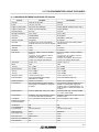
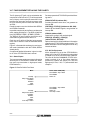
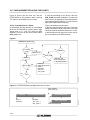
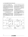
APPLICATION NOTE V.17 FAX EQUIPMENT REPLACING THE R144EFX WITH THE ST75C52/520 By Laurent CLARAMOND and Joël HULOUX SUMMARY Page I PRELIMINARY . . . . . . . . . . . . . . . . . . . . . . . . . . . . . . . . . . . . . . . . . . . . . . . . . . . . . . . . 2 II II.1 II.2 II.3 INTRODUCTION. . . . . . . . . . . . . . . . . . . . . . . . . . . . . . . . . . . . . . . . . . . . . . . . . . . . . . . OVERALL . . . . . . . . . . . . . . . . . . . . . . . . . . . . . . . . . . . . . . . . . . . . . . . . . . . . . . . . . . . . A FEW MODIDIFICATIONS IN THE SOFTWARE . . . . . . . . . . . . . . . . . . . . . . . . . . . . . HARDWARE EVOLUTIONS . . . . . . . . . . . . . . . . . . . . . . . . . . . . . . . . . . . . . . . . . . . . . . 2 2 2 2 III COMPARISON BETWEEN R144EFX AND ST75C52/520 . . . . . . . . . . . . . . . . . . . . . . 3 IV FEATURES REQUIRED FOR FAX COMMUNICATIONS . . . . . . . . . . . . . . . . . . . . . . . 4 V DATA SHEET AND USER’S MANUAL GUIDE LINE . . . . . . . . . . . . . . . . . . . . . . . . . . 4 VI SOFTWARE GUIDE LINE . . . . . . . . . . . . . . . . . . . . . . . . . . . . . . . . . . . . . . . . . . . . . . . 4 VI.1 VI.2 VI.3 VI.4 VI.5 USER INTERFACE. . . . . . . . . . . . . . . . . . . . . . . . . . . . . . . . . . . . . . . . . . . . . . . . . . . . . INTERRUPTIONS. . . . . . . . . . . . . . . . . . . . . . . . . . . . . . . . . . . . . . . . . . . . . . . . . . . . . . PARALLEL EXCHANGE IN SYNCHRONOUS AND IN HDLC MODE . . . . . . . . . . . . . . STATUS REPORT . . . . . . . . . . . . . . . . . . . . . . . . . . . . . . . . . . . . . . . . . . . . . . . . . . . . . G3 FAX EQUIPMENT . . . . . . . . . . . . . . . . . . . . . . . . . . . . . . . . . . . . . . . . . . . . . . . . . . . 5 5 7 8 8 VII FLAG DETECTION. . . . . . . . . . . . . . . . . . . . . . . . . . . . . . . . . . . . . . . . . . . . . . . . . . . . . 9 VII.1 VII.2 VII.3 VII.3.1 VII.3.2 V.21 CHANNEL 2 FLAG 7E DETECTION . . . . . . . . . . . . . . . . . . . . . . . . . . . . . . . . . . . FLAG DETECTION IN V.21 CHANNEL 2 MODE . . . . . . . . . . . . . . . . . . . . . . . . . . . . . . FLAG DETECTION IN HIGH SPEED MODE . . . . . . . . . . . . . . . . . . . . . . . . . . . . . . . . . Flag Detection at the Beginning of C Phase or TCF Reception . . . . . . . . . . . . . . . . . . . Flag Detection in C Phase . . . . . . . . . . . . . . . . . . . . . . . . . . . . . . . . . . . . . . . . . . . . . . . 9 9 9 9 10 VIII EQUALIZER AT RECEPTION SIDE . . . . . . . . . . . . . . . . . . . . . . . . . . . . . . . . . . . . . . . 11 IX HOW TO ADJUST THE TRANSMIT LEVEL . . . . . . . . . . . . . . . . . . . . . . . . . . . . . . . . . 12 X HARDWARE GUIDE LINE . . . . . . . . . . . . . . . . . . . . . . . . . . . . . . . . . . . . . . . . . . . . . . . 12 AN814/0695 1/13 V.17 FAX EQUIPMENT REPLACING THE R144EFX I - PRELIMINARY The ST75C52/520 are a monolithic complete V.17 fax modem which is a superset of the R144EFX. All functions found in the R144EFX can be found in the ST75C52/520, plus a few additional ones (class detection, 16 tone detectors, analog DAC for eyediagram, etc) as you will see in the chapter III table. Although similar, the ST75C52/520 are not a plugin replacement for R144EFX. You will need a few software and hardware adjustments, and with our help, it will cost you less than two man-months to do it. A small effort, compared to your benefits. If you are thinking about integrating the ST75C52/520 with your prefered MCU and ASIC, call us immediately. II - INTRODUCTION II.1 - Overall This application note describes the way to replace the ROCKWELL R144EFX by the SGS-THOMSON ST75C52/520 in a V.17 FAX equipment system. This application note uses information detailed in the ST75C52/520 Data Sheet and User’s Manual. First, you will find comparison on the features of the ST75C52/520 and the R144EFX. Second, will be listed the features required to implement FAX communications. Third, will be presented to the user the different chapters in the ST75C52/520 and User’s manual where information was detailed. At the end of this application note is presented a software and hardware user’s guide. II.2 - A Few Modidifications in the Software The user’s fax software can be divided in two parts. The first part which is the main and the biggest is completly independent of the modem chip and is in charge of the following task : - User interface (keyboard, screen, printer). 2/13 - ECM, T30, T4. Real time kernel. Control. ... Layers 2 and 3 are in this part of the software. This software can be reused in the final application without any modification and any perturbation when running in V.17 fax equipment including a ST75C52/520 modem chip. The second part (which is the smallest) is dependent of the modem chip and includes the driver routines needed to provide a complete list of services to the layer 2 and 3. We mainly find the following drivers : - Interrupts driver. - Modem configuration. - Data transfer (emission/reception). - Tone detection/generation. All the modifications will be easily done since : - the ST75C52/520’s software interface is based on COMMAND SET using friendly mnemonics, - interrupts use dedicated registers clearly identified, - data transfer will use FIFO principle to save CPU time. II.3 - Hardware Evolutions Performances and low cost are the two key parameters that have been followed by SGSTHOMSON. The user can to remove the negative power supply (-5V) since the ST75C52/520 needs only one power supply of +5V. The differential analog output and input will increase performances at low level even on a two-layer printed circuit board. EMI problems can be reduced usin g a cr ys tal o f 29 .4912MHz instead 38.00053MHz. V.17 FAX EQUIPMENT REPLACING THE R144EFX III - COMPARISON BETWEEN R144EFX AND ST75C52/520 Features R144EFX ST75C52/520 Package QUIP 64 and PLCC68 PQFP64 Power +5V ±5%, -5V ±5% +5V ±5% Supply Current at 25°C 97mA and 14mA (555mW) 100mA (500mW, 5mW low power mode ) Supply Current at 0°C 105mA and 16mA (605mW) 130mA (650mW) Operating Range 0 to 70°C 0 to 70°C Storage Temperature -55 to 125°C -45° to 125°C Frequency 38.000530MHz 29.4912MHz MCU Bus 65XX/80XX bus MOTOROLA, INTEL bus Interface with DSP 32 registers 60 registers Interrupts 2 interrupts, one can be activated with a selectif mask from one of the 32 registers One interrupt. Six sources with possible individual mask Serial Interface YES YES TX Buffer 1 byte 2 x 8 bytes RX Buffer 1 byte 2 x 8 bytes FAX Group 3 V.33 (14.4, 12kbps, 17000 and 1800Hz) idem V.17 V.17 (14.4, 12, 9.6, 7.2kbps, 1700 and 1800Hz) with short train V.29 (9.6, 7.2, 4.8kbps), no short train V.27ter (4.8, 2.4kbps) with short train V.33 (14.4, 12kbps, 17000 and 1800Hz) idem V.17 V.17 (14.4, 12, 9.6, 7.2kbps, 1700 and 1800Hz) with short train V.29 (9.6, 7.2, 4.8kbps), with short train V.27ter (4.8, 2.4kbps) withshort train Short Train V.27ter, V.17 V.27ter, V.29, V.17 HDLC YES YES TX Level 0 to -15dBm 0 to -48dBm Dynamic Range 0 to -43dBm 0 to -43dBm Turn On -10 to -47dBm -10 to -51dBm Turn Off -10 to -52dBm -15 to -55dBm Reception Timing ±0.01% frequency error ±0.01% frequency error Tone Generator 2 from 0 to 4800Hz (step 0.15Hz), attenuation if f > 300Hz 4 from 0 to 3600Hz (step 1Hz) DTMF Generation Uses the 2 generators Uses 2 of the 4 generators Tone Detector FR1, FR2 and FR3 from 400 to 3000Hz (FR1 and FR2 not available in high speed reception) 2 to 16 detectors programmable from 0 to 3600Hz : 2 if training FAX high speed reception, else 8, 4 if DTMF detection, 16 if tone reception or audio transmission and reception DTMF Detection Gives the DTMF digit. Twist (-8 to +4dB) Gives the DTMF digit. Threshold -35dBm. Ton > 40ms, Twist (±8dB) Flag Detection Available in high speed reception except in V.27 ter short train and tone detection Available in high speed reception, and tone detection mode Voice Mode 7.2, 8 and 9.6kHz on 8 bits till 10 to 16 bits 7.2, 8 and 9.6kHz. A law on 8 bits Equalizers (Transmission and Reception) 4 4 Input/Output NO NO V.23 (Full Duplex) NO YES Eye Monitoring Yes with serial link Yes with analog output Analog Interface Mono Differential Max Output Level ±3.3V ±2.5V Max Input Level 0dBm at RXA ±2.5V Bell 103-V.21 Full Duplex NO YES Class Detection NO YES 3/13 V.17 FAX EQUIPMENT REPLACING THE R144EFX IV - FEATURES REQUIRED FOR FAX COMMUNICATIONS In phase A (T.30 protocol) the modem chip must provide all features to establish or to answer a call. The user will use Tone Detectors for network tones detection (dialtone, busy tone, ring back tone), for answer tone detection (CED 2100Hz tone) and for flag detection. In the calling unit, tone generators will be used to send DTMF digit, and the calling tone (CNG tone at 1100Hz). When on-hook, the modem chip can help the host make incoming call detection. In phase B, D and E (T.30 protocol) the modem chip must be able to send or receive : - In V.21 ch2, - HDLC frame over V.21 ch2 modulation, - TCF frame in high speed mode (only in phase B). In phase C the chip must be able to send or receive in high speed mode (V.27ter, V.29, V.17), and to detect V.21 flag (HDLC fanion) while in high speed mode reception. The user must be able to adjust level in transmission (carrier, tone). Complete HDLC (transmit and receive) function must also be available in high speed mode to allow ECM (Error Correcting Mode). Some others features such as DTMF detection, voice mode may be required in the final application. To use all the above features the user will initialize registers in the DSP and must read status. So, the chip must provide a friendly interface to a host microprocessor. All the above features included in the R144EFX can be easily used with the ST75C52/520. V - DATA SHEET AND USER’S MANUAL GUIDE LINE Firstly the user has to read carefully the ST75C52/520 Data Sheet and User’s Manual. Secondly the user can use the following list which identifies the main chapters in the ST75C52/520 documentation. These chapters detail the features introduced in the previous chapter. 4/13 Digital Interface : - Data Sheet Chapter III - User’s Manual Chapter II.2 User Interface : - Data Sheet Chapter V Analog Interface : - Data Sheet Chapter XII - User’s Manual Chapter VIII Tone Generator : - Data Sheet Chapter IV.2.4 - Data Sheet Chapter VI : • DEFT, Tone, TGEN commands Tone Detector : - Data Sheet Chapter VIII - User’s Manual Chapter V Interruptions : - Data Sheet Chapter V.I.2 Configuration for G3 FAX : - Data Sheet Chapter VI : • HSHK, SYNC, CONF, MODC commands - Data Sheet Chapter VII - User’s Manual Chapter VII HDLC Function : - Data Sheet Chapter VI • FORM, SERIAL commands - Data Sheet Chapter IX - User’s Manual Chapter IV Control in Transmit Mode : - User’s Manual Chapter VI Control in Receive Mode : - User’s Manual Chapter VII PCB Guide Line : - User’s Manual Chapter IX VI - SOFTWARE GUIDE LINE As the main differencesbetween the R144EFX and the ST75C52/520 are found in the software management, we suggest to the user the following steps to understand the ST75C52/520 software interface : 1.Study the User interface, the Command set, the Command Acknowledge. 2.Study the interruptions features. 3.Study the Parallel exchange in synchronous and in HDLC mode. 4.Study the status report. 5.Study the flow scharts for G3 FAX configuration. V.17 FAX EQUIPMENT REPLACING THE R144EFX VI.1 - User Interface The host processor will be connected to the ST75C52/520 using a dual port ram with dedicated memory addresses for : - Command and Parameters, - Command Acknowledge, - Data Tx buffer (transmission), - Data Rx buffer (reception), - Status information, - Interrupt registers. The address space within the host RAM mapping is a 128 byte block requiring 7 address lines instead 5 for the RFX144EFX. The host processor will use commands (with or without parameters) to initialized the modem chip and to start/stop a specific task such as : send a tone, a carrier or detect a tone, a DTMF, a carrier, ... Hereafter is described the syntax for each command : Opcode : Hexadecimal Value X X X X X X X X Parameters : Field Byte Pos Value Definition Name X a..b XX* Explanation of the parameter Field : Byte : Pos : Value : Name of the addressed bit field. Index of the parameter byte (1 to 4). Bit field position inside the parameter byte. Possible values for the bit (resp. bit field). A value followed by a star means a default value. Each command will be acknowledge by the DSP. The host processormust not send a new command without waiting for the acknowledge of the previous command. Figure 1 is summarized the command acknowledge. VI.2 - Interruptions Six sources of interruptions can be used by the software handler routine : Error Tx Buffer : IT0, if errors have occured : IT2, the ST75C52/520 frees one of the 2 Tx buffers Rx Buffer : IT3, the ST75C52/520 has filled one of the 2 Rx buffers Status byte : IT4 to signify that the modem status has changed Low power mode : IT5 when the ST75C52/520 has been awakened Command : IT6, th e ST75C52/ 520 is acknowledge ready for a new command One 8 bit source register ITSRCR located at address $50 in the dual port ram memory identifies the source : D0 = 1 IT0 pending D1 Not used D2 = 1 IT2 pending D3 = 1 IT3 pending D4 = 1 IT4 pending D5 = 1 IT5 pending D6 = 1 IT6 pending Figure 1 MCU DUAL PORT RAM Parameters Write Parameters (Optional) COMPAR[0..3] Command Write Command COMSYS COMREP[0..1] (Optional) Must Wait Acknowledge Before Sending a New Command (Optional) AN814-01.EPS COMACK Raises Interrupt 5/13 V.17 FAX EQUIPMENT REPLACING THE R144EFX The interrupt source will be reset and acknowledge by writing a $00 at one of the memory location $40 to $46 (Reset Interrupt registers ITREST[0..6]) in the dual port ram memory. ITREST[0] at address $40 is dedicated to IT0. ITREST[2] at address $42 is dedicated to IT2. ... ITREST[6] at address $46 is dedicated to IT6. Figure 2 is an example for IT2. All sources of interrupt can be masked individually or globaly with the interrupt mask register ITMASK located at the address $4F in the dual port ram memory. ITMASK register definition : D7 = 0 All interrupts are masked (global mask) D6 = D7 = 1 IT6 enable D5 = D7 = 1 IT5 enable D4 = D7 = 1 IT4 enable D3 = D7 = 1 IT3 enable D2 = D7 = 1 IT2 enable D1 Not used must be equal to 0 D0 = D7 = 1 IT0 enable Even if an interrupt is masked, the DSP will always set the corresponding bit in the source register (ITSRCR) to allow polling by the host processor. Figure 3 illustrates for IT2 and IT3 the interruption principle, the user could easily transpose this principle to the other interrupts : - IT2 and IT3 are set by the DSP, - IT2 and IT3 are cleared and acknowledged by the host processor, - ITSRCR is only read by the host processor, - ITMASK is read or write by the host processor. Figure 2 MCU Interrupt DUAL PORT RAM (DSP) Raises IT2 Read ITSRCR Gives Source Register Value Acknowledge IT2, Writing 00 into ITRST[2] AN814-02.EPS Execute Tx Interrupt Routine Clear IT2 Figure 3 ITRES2 (Write Only) R Q S (Tx Buffer Emptied) ITRES3 (Write Only) R Q S From ST75C52 Buffer (Rx Buffer Filled) ITSRCR (Read Only) 6 5 4 3 2 1 0 ITMASK (Read Write) 7 6 5 4 3 2 1 0 6/13 AN814-03.EPS SINTR V.17 FAX EQUIPMENT REPLACING THE R144EFX VI.3 - Parallel Exchange in Synchronous and in HDLC Mode Data Tx Buffer : The R144EFX uses only one TX buffer of one byte in parallel transmission. This architecture is very simple since the DSP has to write succesive bytes at the same address. The drawback is that the R144EFX will raise an interrupt every sent byte. To save MCU (host processor) time the principle is quite different with a ST75C52/520. Two Tx buffers will be used in parallel transfer, TX_BUFFER_0 called DTTBF0 and TX_BUFFER_1 called DTTBF1. Each Tx buffer contains 8 bytes. The host processor can write one to eight bytes in the same buffer. The Tx interrupt (IT2) will only be raised when the complet TX buffer will be empty (e.g for TX buffers filled with 8 bytes the IT2 will be activated every 8 bytes). As this principle save MCU time between two interrupts, the host processor could be more efficiency used for other main tasks such as Error Correcting Mode (ECM), ... One status byte DTTBS0 is dedicated to DTTBF0 and another DTTBS1 is associated with DTTBF1. Parallel transmission must be initialized with SERIAL, FORM and XMIT commands. In parallel transmission the two buffers must be used, always starting with buffer 0. The host processor must send data alternatively into DTTBF0, DTTBF1, DTTBF0, DTTBF1, DTTBF0, ... The host processorwrites data into a Tx buffer then writes the number of bytes into the dedicated status. The DSP reads the Tx buffer and clears the dedicated status, then raises IT2. Figure 4 is illustrated the exchange in transmit parallel mode (initialization with the FORM, SERIAL and XMIT was already done). Complet and detailed information is given in chapter IV of the ST75C52/520 User’s Manual. Data Rx Buffers : The R144EFX uses only one RX buffer of one byte in parallel reception. This architecture is very simple since the DSP has to read succesive bytes at the same address. The drawback is that the R144EFX will raise an interrupt every received byte. To save MCU (host processor) time the principle is quite different with a ST75C52/520. Two RX buffers will be used in parallel transfer, RX_BUFFER_0 called DTRBF0 and RX_BUFFER_1 called DTRBF1. Each Rx buffer contains 8 bytes. The host processor will generaly read eight bytes in the same buffer except if the modem chip detects a loss of carrier. One status byte DTRBS0 is dedicated to DTRBF0, and another DTRBS1 is dedicated to DTRBF1. Figure 4 : Data Tx Buffer Flow Chart MCU Step-1-MCU Fill DTTBF0 Write DTTBS0 Interrupt DUAL PORT RAM (DSP) Step-1-DSP Reads DTTBS0 Reads DTTBF0 Clears DTTBS0 Raises IT2 Step-2-MCU Fill DTTBF1 Interrupt Goto Step-1-MCU Step-2-DSP Reads DTTBS1 Reads DTTBF1 Clears DTTBS1 AN814-04.EPS Write DTTBS1 Raises IT2 Goto Step-1-DSP 7/13 V.17 FAX EQUIPMENT REPLACING THE R144EFX The Rx interrupt (IT3) will only be raised when the complet RX buffer will be full (IT3 will be activated every 8 bytes). As this principle saves MCU time between two interrupts, the host processor could be more efficiency used for other main tasks such as ECM, ... Parallel reception must be initialized with SERIAL and FORM commands. In parallel reception the two buffers must always be used, starting with buffer 0. The DSP will alternatively fill DTRBF0, DTRBF1, DTRBF0, DTRBF1, ... The DSP will fill one Rx buffer, then fill the dedicated status register and then raises IT3. Each time an Rx buffer is filled the host processor must read it and then clear the dedicated status register. Figure 5 is illustrated the exchange in receive parallel mode (initialization with the FORM, SERIAL already done). Complet and detailed information is given in chapter IV of the ST75C52/520 User’s manual. VI.4 - Status Report The host processor needs some status information writen by the ST75C52/520 to folllow tone detection result, synchronisation in high speed mode, DTMF detection, ... For that purposethe ST75C52/520 provides following status : ERROR STATUS (address $08) : Provides information about error, can generate an interrupt IT0. STATUS[0], STATUS[1] (addresses $09, $0A) : Contain all the Modem signals, can generate an interrupt IT4. STAQUA (address $0B) : Contains the quality of the received signal. STAOP[0], STAOP[1], STAOP[2] (addresses $0C, $0D, $0E) : Optional status that contain additional information regarding the ST75C52/520 operating mode. This default information can be changed to monitor any internal variables. VI.5 - G3 Fax Equipment All the information to set up the ST75C52/520 in phase A,B,C,D and E (T.30 protocol)are described in chapter III of the ST75C52/520 User’s Manual. The user will find the COMMAND, STATUS information required. A lot of flow charts detail the procedure to initialize low speed (V.21 ch2) and high speed (V.27ter, V.29 , V.17) transmission and reception. Figure 5 : Data Rx Buffer Flow Chart Interrupt Step-1-MCU Read DTRBS0 DTRBF0 Clear DTRBS0 Interrupt Step-2-MCU Read DTRBS1 DTRBF1 Clear DTRBS1 Goto Step-1-MCU 8/13 DUAL PORT RAM (DSP) Fill DTRBF0 Step-1-DSP Fill DTRBS0 Raise IT3 Fill DTRBF1 Step-2-DSP Fill DTRBS1 Raise IT3 Goto Step-1-DSP AN814-05.EPS MCU V.17 FAX EQUIPMENT REPLACING THE R144EFX VII - FLAG DETECTION Figure 6 This chapter describes the way to use the flag_detection provided by the ST75C52/520 status report which will be used by a Host micro-controller. V.21 Channel 2 CONF 0F 0D 00 00 SYNC 1 The ST75C52/520 provides in the STATUS1 (address $0A in the host interface) the STA_FLAG bit. STATUS1 is an 8 bit register that can be read (only) by the host. Bit position 7 corresponds to the MSB and bit position 0 corresponds of the LSB. I n this register bit 6 (position 6) is called STA_FLAG (valid only in FAX modem and tone mode). STA_FLAG equal to 1 means that a V.21 ch2 flag is detected. Carrier Detect ? STA_109 Flag Detected ? STA_FLAG Three flags are necessary to validate V.21 flag. So minimum timing for V.21 flag detection is : AN814-06.EPS VII.1 - V.21 Chanel 2 Flag 7E Detection Flag Detected 3.3ms x 8 x 3 = 79.2ms. At this optimum timing you have to add the response time for the filters and the time for synchronisation of state machine at the beginning of the flag. The overall detection of V.21 ch2 flag is between 92 and 98ms. The overall time for loss of V.21 ch2 flag is between 17 and 25ms. VII.2 - Flag Detection in V.21 Channel 2 Mode If the ST75C52/520 is set to receive in V.21 channel 2 mode, the V.21 flag detector is always available. The following flow chart shows how the host must used the ST75C52/520 to detect V.21 ch2 flag while receiving in low speed mode (See Figure 6). VII.3 - Flag Detection in High Speed Mode VII.3.1 - Flag Detection at the Beginning of C Phase or TCF Reception In such a case the ST75C52/520 is setting up to receive in V.27, V.29 or V.17. When the host starts the synchronisation of the reception sending the SYNC 1 command to the ST75C52/520, the internal DSP executes two tasks in which the V.21 ch2 flag detection is activated : - looking for V.21 ch2 signal, - looking for training in high speed mode. The V.21 ch2 flag detection is not available when the ST75C52/520 is in data mode (the training is completed, the carrier detect signal and the STA_109 are true indicating a received high speed modulation). Figure 7 shows when the flag detection is available. Figure 7 : ST75C52/520 High Speed Received Sequence Flag Detection Available CONF SYNC 1 Data in High Speed Mode Flag Detection Disabled AN814-07.EPS Training STA_109 Carrier Detect 9/13 V.17 FAX EQUIPMENT REPLACING THE R144EFX Figure 8 shows how the host can use the ST75C52/520 for flag detection when receiving TCF frame or at the beginning of C phase. It could be interesting for the host to have the STA_FLAG information available in C phase just after a loss of the high speed carrier because the next received signal could be a V.21 ch2 instead a high speed carrier without a training. Figure 9 summarizes the two cases. In the first case the transmit unit has cut the high speed transmission (which causes the loss of the carrier) and start to send HDLC frames in V.21 ch2. In the second case the loss of the carrier may be due to a problem on the PSTN network. VII.3.2 - Flag Detection in C Phase As said above the flag detection is not available while the ST75C52/520 is receiving data in high speed mode (V.17, V.29, V.27) since the DSP disables it as soon as the carrier detect status (STA_109) is true. Figure 8 CONF (V.27, V.29, V.17) V.17 Short Train Yes No No No STA_FLAG SYNC 1 Yes STA_FLAG No Yes Wait STA_109 then Receive Data in High Speed Mode SYNC 00 CONF 0F 0D 00 00 SYNC 1 WAITING : STA_109 STA_FLAG P2s AN814-08.EPS No PNDETS MODC 40 00 Figure 9 : ST75C52/520 Received Signal with Loos of Carrier Loss of Carrier (STA_109F = 0) Training Data in High Speed Mode V.21 Channel 2 Flag Start of Reception 10/13 Reception STA_109 = 1 STA_109F = 1 Data in High Speed New Received Signal AN814-09.EPS or V.17 FAX EQUIPMENT REPLACING THE R144EFX Figure 10 gives to the user the way to be able to detect V.21 ch2 flag just after a loss of high speed carrier. To enable and disable the flag detection the host will performe a Memory Write (MW) command (see Table 1 for addresses and parameters). As the short train is only used in C phase while receiving in V.17 mode the host can avoid to send the Enb short sequence to the ST75C52/520 in V.29 and V.27. This flow chart (Figure 10) could be used in phase B but take care that the Enb short sequence must only be sent in C phase. In Fax application the coefficients are firstly computed when receiving the TCF frame (continuous 0 during 1.5s) in phase B of the T.30 protocol. As the DSP rev 1.0 software takes more than 1.5s when in data mode to compute the coefficients of the equalizer the host must reduce these time sending to the DSP two memory write (MW) command. The two MW must be sent just after STA_109 equals 1 indicating a high speed modulation signal : VIII - EQUALIZER AT RECEPTION SIDE The DSP provides an equalizer function in the reception section. It computes the coefficients of this equalizer firstly during the training and secondly during the first seconds of the data mode (carrier detect signal and STA_109 are true). The DSP will take now 1.2s after the beginning of the data mode (STA_109 = 1) to compute the coefficients of the equalizer. First MW MW E3 16 01 00 Second MW MW E3 16 B0 04 For DSP rev 1.1 software the problem is solved and the two MW need not be sent by the host. Figure 10 CONF (V.17, V.29, V.27) Enb Short SYNC 1 Yes SYNC 0 CONF 0F 0D 00 00 No No STA_109 No STA_109 Yes V.21 Ch2 Disable Flag Yes Enable Flag (1) Yes Yes No STAQUA ≥ 3F Yes STA_109F STA_109F No No AN814-10.EPS STA_FLAG Enable Flag (2) Table 1 V.17 CONF 0F 09 00 04 MW 15 10 14 00 MW 15 10 14 00 MW 15 10 04 00 MODC 40 00 V.29 CONF 0F 08 00 01 MW 15 10 12 00 MW 15 10 10 00 MW 15 10 00 00 MODC 00 00 V.27 CONF 0F 07 40 00 MW 15 10 12 00 MW 15 10 10 00 MW 15 10 00 00 MODC 00 00 AN814-01.TBL CONF HIGH SPEED Enbl Flag (1) Enbl Flag (2) Disable Flag Enb Short 11/13 V.17 FAX EQUIPMENT REPLACING THE R144EFX IX - HOW ADJUST THE TRANSMIT LEVEL As explained in the ST75C52/520 User’s Manual in chapter VI.3 the user can adjust the level on the line using the SETGN command. Like that the user chooses an attenuation in the transmit section (no attenuation means a 0dB value for the parameter of the SETGN command). There is no limitation for the attenuation values. You can use different attenuationvalues with a step less than 1dB between each value. The USER’S MANUAL gives as example the value for attenuation between 0dB and -14dB with a step of 1dB. How to compute the value of the parameter for the SETGN command ? As the attenuation is provided by a gain in the transmit section you must know the value of the next gain which gives the wanted attenuation.0dB attenuationmeans a unit gain (Gt = 1). For 0dB the value of the SETGN parameter is 7FFF (hexa decimal value) or 32768 (decimal value). Suppose you would like a -10dB attenuation, in such a case your attenuation gain will have a value of Gt = 0.6065. The value of the SETGN parameter will be equal to 32768 x 0.6065 (decimale value) or 287A (hexadecimal value). Now the host has only to send SETNG 287A (command and parameter) to the DSP to set up the attenuation gain at the wanted value. X - HARDWARE GUIDE LINE The ST75C52/520 can be connected to a host processor using INTEL or MOTOROLA bus. A synchronisation between the ST75C52/520 and the host is provided with SDTACK (for data acknowledge) and SINTR (for interrupts) signals which are both open drain. The analog interface is detailed in chapter VI, VII, VII of the ST75C52/520 User’s Manual. Here, we briefly cover the basic schematics and hybrid interface tuning (See Figure 11). Figure 11 22kΩ 220pF R’ TXA1 4 11 22kΩ 1.2kΩ 3 RXA2 1 2 2 1 3 U1A MC33174 11 R R3 4 U1A MC33174 R1 2.2nF V/2 VCM VCM R2 680pF 4 13.2kΩ 22kΩ U1B MC33174 -V/2 R 7 2 1 3 11 R’ 22kΩ R1 11 6 TXA2 2.2nF R3 5 4 220pF RXA1 1.2kΩ U1A MC33174 TIP VT In this example the MC33174 is powered between 0VA and +5VA 12/13 TRANSFORMER RING AN814-11.EPS 13.2kΩ V.17 FAX EQUIPMENT REPLACING THE R144EFX Components : All resistors are 1% tolerance Operational Amplifier SGS-THOMSON : MC33174 Tuning : Return Loss : R0 R3 = 2 Where R0 is the value for the best return loss v ersu s the re ferenc e in peda nce Z0. An d Z0 = 600Ω or Complex Impedance Duplexor : Z0 ⋅ V VT = (Z0 + R0) VT Z0 Coef = = V Z0 + R0 Z0 = 600Ω, R0 = 440Ω Coef = 0.577 R = 23.08kΩ and R’ = 40kΩ Transmit Gain : Tx_Gain = 22kΩ/13.2kΩ Today tuned to have -9dBm on the line. To transmit at 0dBm you must : - Replace the two 13.2kΩ 1% by two 4.64kΩ 1%. - Replace the two 220pF by 47pF. - Power supply of the Amplifier : +V and -V. To have the best rejection : R’ = Example 1: Z0 = 600Ω, R0 = 600Ω Coef = 0.5 R = 20kΩ and R’ = 40kΩ Example 2 : R Coef Receive Gain : Rx_Gain = 1 + R1 R2 2 Typical values R1 = 15kΩ, R2 = 82kΩ Information furnished is believed to be accurate and reliable. However, SGS-THOMSON Microelectronics assumes no responsibility for the consequences of use of such information nor for any infringement of patents or other rights of third parties which may result from its use. No licence is granted by implication or otherwise under any patent or patent rights of SGS-THOMSON Microelectronics. Specifications mentioned in this publication are subject to change without noti ce. This publication supersedes and replaces all information previously supplied. SGS-THOMSON Microelectronics products are not authorized for use as critical components in life support devices or systems without express written approval of SGS-THOMSON Microelectronics. 1995 SGS-THOMSON Microelectronics - All Rights Reserved Purchase of I2C Components of SGS-THOMSON Microelectronics, conveys a license under the Philips I2C Patent. Rights to use these components in a I2C system, is granted provided that the system confo rms to the I2C Standard Specifications as defined by Philips. SGS-THOMSON Microelectronics GROUP OF COMPANIES Australia - Brazil - China - France - Germany - Hong Kong - Italy - Japan - Korea - Malaysia - Malta - Morocco The Netherlands - Singapore - Spain - Sweden - Switzerland - Taiwan - Thailand - United Kingdom - U.S.A. 13/13