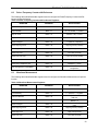
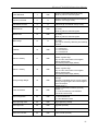
1
 8B SLX300
Data Acquisition System
Software User Manual
8B isoLynx® SLX300 Software User Manual
®
8B isoLynx SLX300 Software User Manual
MA1032 Rev. A – July 2010
© 2010 Dataforth Corporation. All Rights Reserved.
The information in this manual has been checked carefully and is believed to be accurate; however,
Dataforth assumes no responsibility for possible inaccuracies or omissions. Specifications are subject to
change without notice.
The information, tables, diagrams, and photographs contained herein are the property of Dataforth
Corporation. No part of this manual may be reproduced or distributed by any means, electronic,
mechanical, or otherwise, for any purpose other than the purchaser’s personal use, without the express
written consent of Dataforth Corporation.
isoLynx® is a registered trademark of Dataforth Corporation.
Windows® is a registered trademark of Microsoft Corporation.
LabVIEW™ is a trademark of National Instruments Corporation.
Modbus® is a registered trademark of the Modbus Organization, Inc.
ii
8B isoLynx® SLX300 Software User Manual
Table of Contents
1.0 Introduction ...................................................................................................................................... 1 1.1 Related Documents ....................................................................................................................... 1 1.2 Document Conventions ................................................................................................................. 1 2.0 Device Operation ............................................................................................................................. 2 2.1 Device Configuration ..................................................................................................................... 2 2.2 2.2.1 Reading Analog Data ........................................................................................................ 3 2.2.2 Writing Analog Data .......................................................................................................... 4 2.2.3 Cold Junction Compensation (CJC) .................................................................................. 5 2.2.4 Alarms ............................................................................................................................... 5 2.3 3.0 Analog Data............................................................................................................................... 2 Digital Data ................................................................................................................................ 5 2.3.1 Reading Digital Data ......................................................................................................... 5 2.3.2 Writing Digital Data............................................................................................................ 5 2.3.3 Digital I/O Special Functions ............................................................................................. 5 8B isoLynx® SLX300 Communication Interface Configuration ........................................................ 8 3.1 Modbus Protocol ........................................................................................................................... 8 3.1.1 Modbus RTU ..................................................................................................................... 8 3.1.2 Modbus TCP ..................................................................................................................... 8 3.1.3 Modbus Function Codes ................................................................................................... 8 3.1.4 Modbus Addresses............................................................................................................ 8 3.1.5 Modbus Exceptions ........................................................................................................... 9 3.2 Changing the Communication Protocol Settings .......................................................................... 9 3.3 Resetting Communication Parameters to Factory Default Values ............................................ 9 3.4 Modbus Slave ID ....................................................................................................................... 9 3.5 Modbus RTU Parameters ............................................................................................................. 9 3.5.1 Modbus RTU Parameter Registers ................................................................................. 10 3.6 Modbus TCP Parameters ............................................................................................................ 10 3.6.1 4.0 Modbus TCP Parameter Registers ................................................................................. 10 Analog (ADC / DAC) Channel Configuration ................................................................................. 12 4.1 Analog (ADC / DAC) Channel States ...................................................................................... 12 4.2 Analog ADC Channel Average Weights ................................................................................. 13 4.2.1 4.3 Analog DAC Channel Default Outputs .................................................................................... 13 4.3.1 4.4 Analog Channel Average Weight Registers .................................................................... 13 Analog Channel Default Output Registers ...................................................................... 13 Cold Junction Compensation (CJC) ........................................................................................ 14 4.4.1 CJC Channel Control Registers ...................................................................................... 14 4.4.2 CJC Type Registers ........................................................................................................ 14 iii
8B isoLynx® SLX300 Software User Manual
4.4.3 4.5 Alarms ..................................................................................................................................... 15 4.5.1 Alarm Channel Control Registers.................................................................................... 15 4.5.2 Alarm Limit Registers ...................................................................................................... 17 4.5.3 Alarm Status Registers ................................................................................................... 17 4.6 5.0 Save Analog Channel Parameters to EEPROM ..................................................................... 17 Digital I/O Channel Configuration .................................................................................................. 19 5.1 Digital I/O Channel States ....................................................................................................... 19 5.1.1 5.2 5.3 7.0 Digital Channel Default Output Registers ....................................................................... 20 Save Digital I/O Setting to EEPROM ...................................................................................... 20 Digital I/O Special Function Configuration ..................................................................................... 21 6.1 Pulse / Frequency Counter ..................................................................................................... 22 6.2 Pulse / Frequency Counter with De-bounce ........................................................................... 23 6.3 Waveform Measurement ......................................................................................................... 23 6.4 Time Between Events ............................................................................................................. 24 6.5 Frequency Generator .............................................................................................................. 24 6.6 PWM Generator ...................................................................................................................... 25 6.7 One-Shot Pulse Generator...................................................................................................... 25 Analog Input Scan Configuration ................................................................................................... 26 7.1 Scan Mode .............................................................................................................................. 26 7.1.1 7.2 Scan Mode Register ........................................................................................................ 26 User-Defined Scan Parameters .............................................................................................. 27 7.2.1 8.0 Digital I/O Channel State Registers ................................................................................ 19 Digital Output Default Outputs ................................................................................................ 19 5.2.1 6.0 CJC Lower and Upper Range Registers ......................................................................... 14 User-Defined Scan Parameter Registers ........................................................................ 28 Reading Analog Data ..................................................................................................................... 29 8.1 Continuous Scan Data ............................................................................................................ 29 8.1.1 Continuous Scan Data Registers .................................................................................... 29 8.2 User-Defined Scan Data ............................................................................................................. 29 9.0 iv
8.2.1 Starting a User-Defined Scan ......................................................................................... 30 8.2.2 Polling the Scan Count Register ..................................................................................... 30 8.2.3 Reading Data from the Scan Data Register .................................................................... 30 8.2.4 User-Defined Scan Data Registers ................................................................................. 30 Writing Analog Output Data ........................................................................................................... 31 9.1 Write Analog Output Data Registers ....................................................................................... 31 9.2 Analog Output DAC User-Defined-Scan (Burst Mode) ........................................................... 31 9.2.1 4x16k Buffer Registers .................................................................................................... 31 9.2.2 DAC Interval Register ..................................................................................................... 32 9.2.3 DAC Burst Control Register ............................................................................................ 32 8B isoLynx® SLX300 Software User Manual
10.0 Digital Data and I/O Special Functions .......................................................................................... 33 10.1 Digital Data Read and Write.................................................................................................... 33 10.2 Digital I/O Special Functions ................................................................................................... 33 11.0 10.2.1 Pulse / Frequency Counter Function............................................................................... 33 10.2.2 Pulse / Frequency Counter with De-bounce Function ................................................ 34 10.2.3 Waveform Measurement Function .............................................................................. 34 10.2.4 Time Between Events Function .................................................................................. 35 10.2.5 Frequency Generator Function ....................................................................................... 36 10.2.6 PWM Generator Function ........................................................................................... 36 10.2.7 One-Shot Pulse Generator Function ............................................................................... 37 User Data ....................................................................................................................................... 38 11.1 12.0 Device Information ......................................................................................................................... 39 12.1 13.0 User Data Registers ................................................................................................................ 38 Device Information Registers .................................................................................................. 39 Miscellaneous Function and Control .............................................................................................. 40 13.1 Temperature Sensor ............................................................................................................... 40 13.1.1 13.2 Temperature Sensor Register ..................................................................................... 40 Firmware Resets ..................................................................................................................... 40 13.2.1 Reset Registers ........................................................................................................... 41 14.0 Appendix A: 8B isoLynx® SLX300 Modbus Address Map ............................................................. 42 15.0 Appendix B: 8B isoLynx® SLX300 Throughput .............................................................................. 54 B.1 Test Networks and Test Setup ................................................................................................ 54 B.2 Throughput Descriptors ........................................................................................................... 54 B.3 Command Times ..................................................................................................................... 55 B.4 Command Rates ..................................................................................................................... 55 B.5 Throughput .............................................................................................................................. 56 v
8B isoLynx® SLX300 Software User Manual
About Dataforth Corporation
“Our passion at Dataforth Corporation is designing, manufacturing, and marketing the best possible signal
conditioning, data acquisition, and data communication products. Our mission is to set new standards of
product quality, performance, and customer service.” Dataforth Corporation, with more than a quarter
century of experience, is the worldwide leader in Instrument Class® Industrial Electronics—rugged, high
performance signal conditioning, data acquisition, and data communication products that play a vital role
in maintaining the integrity of industrial automation, data acquisition, and quality assurance systems. Our
products directly connect to most industrial sensors and protect valuable measurement and control
signals and equipment from the dangerous and degrading effects of noise, transient power surges,
internal ground loops, and other hazards present in industrial environments.
Dataforth spans the globe with more than 50 International Distributors and US Representative
Companies. Our customers benefit from a team of over 130 sales people highly trained in the application
of precision products for industrial markets. In addition, we have a team of application engineers in our
Tucson factory ready to solve any in-depth application questions. Upon receipt of a quote or order, our
Customer Service Department provides fast one-day delivery information turnaround. We maintain an
ample inventory that allows small quantity orders to be shipped from stock.
Contacting Dataforth Corporation
Contact Method
E-Mail:
Technical Support
Website:
Phone:
Fax:
Mail:
Contact Information
[email protected]
www.dataforth.com
520-741-1404 and toll free 800-444-7644
520-741-0762
Dataforth Corporation
3331 E. Hemisphere Loop
Tucson, AZ 85706
Errata Sheets
Refer to the Technical Support area of Dataforth’s website (www.dataforth.com) for any errata information
on this product.
vi
8B isoLynx® SLX300 Software User Manual
1.0
Introduction
The 8B isoLynx® SLX300 is a fast, intelligent, fully isolated data acquisition system providing superior
reliability, accuracy, and isolation for a wide range of rugged industrial applications. The flexible, modular
design combines eight SCMD digital I/O channels, four 8B analog output channels and twelve 8B analog
input channels into one single board.
The 8B isoLynx® implements the industry standard Modbus RTU and TCP protocols, thereby enabling
communication with a wide variety of existing third-party software drivers and HMI/SCADA packages.
Dataforth offers a Windows based, free Configuration Software Tool which makes it easy to make a few
basic system connections and quickly start taking measurements.
The 8B isoLynx® is factory configured to communicate to a host PC using RS-232, RS-485, or USB serial
links or Ethernet as its physical layer. Up to 16 systems can be multi-dropped on the RS-485 serial link.
1.1
Related Documents
The following documents are available from Dataforth Corporation:
•
MA1029 SLX300 Configuration Software Tool User Manual
•
MA1030 SLX300 Quick Start Guide
•
MA1031 SLX300 Hardware User Manual
•
MA1033 SLX300 LabVIEW VI Examples User Manual
The following documents are available from the Modbus Organization (www.modbus.org):
1.2
•
Modbus Application Protocol Specification, V1.1a, June 2004
•
Modbus over Serial Line Specification & Implementation Guide, V1.0, November 2004
•
Modbus Messaging on TCP/IP Implementation Guide, V1.0a, June 2004
Document Conventions
This document follows the following conventions:
•
Hexadecimal numbers are preceded by the ‘0x’ suffix (e.g., 0xFA02).
•
Binary numbers are preceded by ‘b’ (e.g., b1011).
•
If a given number is not preceded by a suffix, it is a decimal value (e.g., 123).
1
8B isoLynx® SLX300 Software User Manual
2.0
Device Operation
2.1
Device Configuration
An 8B isoLynx® SLX300 system must be configured before use. Configuration is best described in two
steps: communication interface configuration and channel configuration.
The system ships with factory default communication parameter settings. These parameters and their
factory defaults are described in Section 3.0 8B isoLynx® SLX300 Communication Interface
Configuration. If the factory default settings are appropriate, communication interface configuration can
be skipped.
Channel configuration cannot be skipped. The analog channel may need to be configured for cold
junction compensation (CJC) if an 8B thermocouple input module is used or for alarm if the alarm function
is used, etc. At a minimum, digital I/O channel states must be configured to enable read or write access
to them. Each digital I/O channel can be configured in one of several states: vacant, input, output, or
alarm. The factory default state for all digital I/O channels is vacant.
An analog channel refers to the physical slot on the system board where an 8B module can be installed.
®
There are a total of 12 analog input and 4 analog output channels on the 8B isoLynx SLX300. The 12
analog ADC channels are fixed as inputs and the 4 analog DAC channels are fixed as outputs; they do
not need to be configured as inputs or outputs.
A digital channel refers to the physical slot on the system board where an SCMD module can be installed.
There are a total of 8 digital channels on the 8B isoLynx® SLX300. A digital channel should be configured
as an input if an SCMD digital input module is installed at that location. Doing so enables read access to
the channel. Similarly, a digital channel should be configured as an output if an SCMD digital output
module is installed at that location to enable write access to the channel.
Other channel parameters can be configured, such as input average weights for analog channels, analog
and digital default output values, and digital I/O special function(s), but it is not absolutely necessary to do
so. Analog channel parameters and their configuration are described in Section 4.0 Analog (ADC/DAC)
Channel Configuration. Digital channel parameters and their configuration are described in Section 5.0
Digital I/O Channel Configuration. Digital I/O special function parameters and their configuration are
described in Section 6.0 Digital I/O Special Function Configuration. Analog and digital channel
configurations can be reset to factory default settings by issuing reset commands to the appropriate
registers (see Section 13.2 Firmware Resets).
2.2
Analog Data
Analog data is read from analog input channels and written to analog output channels.
Analog input data values are 12-bit unsigned numbers that represent voltages in the 0 to +5V range.
0x0000 represents 0V, and 0x0FFF represents +5V. Each increment or count in the data value
represents a 1.22mV step in voltage.
Analog output data values are 12-bit unsigned numbers that represent voltages in the 0 to +5V range.
0x0000 represents 0V, and 0x0FFF represents +5V. Each increment or count in the data value
represents a 1.22mV step in voltage.
Analog data always represents a voltage. How this value maps to actual engineering units depends on
the 8B module from which the data is read or to which the data is written.
2
8B isoLynx® SLX300 Software User Manual
Example 1: Data from an 8B37J thermocouple input module is read. This module has a -100°C to
+760°C input range and a 0 to +5V output range. A data value of 0x0000 (0V) corresponds
to an input of -100°C, and a data value of 0x0FFF (+5V) corresponds to an input of +760°C.
Example 2: Data is written to an 8B39-01 current output module. This module has a 0 to +5V input range
and a 4 to 20mA output range. A data value of 0x0000 (0V) corresponds to an output of
4mA, and a data value of 0x0FFF (+5V) corresponds to an output of 20mA.
Only 8B input modules with a unipolar 0 to 5V output can be used in the 8B isoLynx® SLX300 system.
The system has over-range clamps and protection but the use of a module with output range beyond this
limit may damage the system after prolonged operation.
2.2.1
Reading Analog Data
Analog data can be read from analog input and analog output channels. Reading data from an analog
output channel simply returns the last value written. How data is read from analog input channels
depends on the selected scan mode. The 8B isoLynx® SLX300 supports two scan modes which are
described below. For further details, see Section 8.0 Reading Analog Data.
2.2.1.1 Continuous Scan Mode
In this mode, the system continuously scans all 12 analog input channels, converting the installed 8B
module output voltages to digital data values at a fixed scan rate of 6000 samples per second (1 sample
every 160µs). The 12 analog input channels are sampled one at a time in sequential order. Once all
analog inputs have been sampled, the scan restarts at the first analog input.
Since the scan rate is fixed and all analog input channels are scanned, the rate at which a given input
channel is sampled is dependent on the number of analog inputs. The formula for the single channel
sample rate is given below:
Sample Rate = 1 / (166.7µs x 12) = 500 samples / second
Analog data values are stored in a circular SRAM buffer. Only one conversion result per channel is
stored at a time. New conversion results overwrite a channel’s previous conversion result. The most
recent conversion results may be retrieved at any time with a Modbus Read Registers command.
In addition, a running average is calculated for each analog input every time a channel is sampled. The
weight used in the running average calculation is configurable on a per-channel basis (see Section 4.0
Analog (ADC/DAC) Channel Configuration). Running average results are stored in a circular SRAM
buffer and can be accessed with a Modbus Read Registers command. The running average formula is:
Average = Average + ((Sampled Value - Average) ÷ Average Weight)
Maximum and minimum values are also maintained for each analog input and stored in circular SRAM
buffers. The maximum and minimum values can be read at any time with a Modbus Read Registers
command to the appropriate address. The average value, maximum value or minimum value can be
reset at any time with a Modbus Write Registers command.
NOTE: Due to the circular buffer architecture of Continuous Scan Mode, if data from a contiguous group
of analog input channels is read, it cannot be determined which channel’s data is the most recent. The
scan could be processing any one of the current analog inputs when the request is received; therefore,
any one of the analog data values might be the most recent.
3
8B isoLynx® SLX300 Software User Manual
2.2.1.2 User-Defined Scan Mode (Burst Scan Mode)
In User-Defined Scan Mode (Burst Scan Mode), analog input channels are not continuously scanned.
Instead, the scan is started and stopped at the direction of the host application. Analog conversion
results are stored in a 192k-word FIFO buffer and can be read either after the scan completes or as data
becomes available. The maximum sample rate is 100k samples / second. This will decrease if additional
signal processing is enabled. Reference Section 7.2 User-Defined Scan Parameters for further details.
Before a User-Defined Scan can be started, a scan list must be configured. This is a list containing up to
48 entries of the 12 analog input channels. Each channel can be listed more than once and channels can
be listed in any order.
A scan interval of as little as10µs and scan buffer memory size up to 192k words can also be configured;
this defines how often the entries in the scan list are scanned and how much of the buffer’s memory is
used. When the defined buffer memory becomes full, the scan is stopped. In addition, a scan count can
be read. The scan counter indicates how many samples are in the scan buffer memory.
A scan is started with a Modbus Write Registers command to a Scan Mode register. The scan continues
until one of the following occurs: 1) the scan-defined buffer memory becomes full, or 2) the scan is
aborted by the user. Due to the FIFO buffer architecture used by the User-Defined Scan Mode,
conversion data is never overwritten. This allows an application to reconstruct a highly-accurate, timecorrelated representation of the signals being measured. More details are given in Section 7.0 Analog
Input Scan Configuration and Section 8.0 Reading Analog Data.
2.2.1.3 Deciding which Scan Mode to Use
For most general purpose signal monitoring applications, Continuous Scan Mode is more than adequate.
Reading the most recent conversion results is like taking a snapshot in time of one or more analog input
signals. Average, maximum, and minimum values give an indication of what the signals are doing over
time. Continuous Scan Mode is also easy to use: just configure the channels and start reading data. The
drawbacks to Continuous Scan Mode are: 1) due to the circular buffer architecture, when a block of
channels is read, there is no way to determine which channel’s data is the most recent, and 2) timing
between scans is fixed.
Applications that require better time-correlation and a fast sampling rate are advised to use the UserDefined Scan Mode. Although average, maximum, and minimum values are not calculated in this mode,
the user can construct a highly accurate representation of the signals in the time-domain. Post
processing of the data can then be performed to derive FFTs, averages, maximums, minimums, etc.
2.2.2
Writing Analog Data
Analog data can be written to analog output channels at any time, regardless of the currently configured
analog input scan mode. See Section 9.0 Writing Analog Output Data for details.
2.2.2.1 DAC Continuous Scan Mode
Once a value is written to an analog output register, an output will stay at the given value until a new
value is written to the register or until the system is reset or power cycled. If reset or power cycle occurs,
the channel will revert to its default output value. Default output values are configurable on a per-channel
basis (see Section 4.0 Analog (ADC/DAC) Channel Configuration). There is no need to refresh analog
®
output channels. A process internal to the 8B isoLynx periodically refreshes all output channels with the
value that was last written.
4
8B isoLynx® SLX300 Software User Manual
2.2.2.2 DAC User-Defined Scan Mode (Burst Scan Mode)
In User-Defined Scan Mode (Burst Scan Mode), analog output data can be preloaded in the 64k buffer
memory. 16k values per channel are allowed. The scan interval is also configurable and can be as small
as 1ms. A scan is started with a Modbus Write Registers command to a Scan Control register.
2.2.3
Cold Junction Compensation (CJC)
The CJC registers must be configured when an 8B37 or 8B47 thermocouple input module is installed in
an analog input channel to allow calculation of the cold junction compensation factors (see Section 4.4
Cold Junction Compensation for details). All standard product 8B thermocouple input modules 8B37x
and 8B47x-xx are supported.
2.2.4
Alarms
The 8B isoLynx® SLX300 allows alarms to be enabled individually on any analog input channel. Input
samples are compared with pre-configured high- and low-level alarm limits or high-high and low-low alarm
limits, and if the limits are exceeded, an alarm condition occurs. When an alarm condition is asserted, the
system will do the following: 1) turn on the System Alarm LED, 2) set appropriate bits in the channel’s
Alarm Status register, and, 3) if enabled, set the corresponding alarm output to the pre-configured analog
or digital alarm output value. No asynchronous communication with the host occurs as this violates the
Modbus protocol..
Tracking and Latched alarm modes are supported on each input channel. In Tracking Mode, the system
will de-assert the alarm condition when the input returns within limits, taking into account the deadband
parameter. When used with an alarm output, this mode allows the user to implement a simple on/off
controller.
In Latched Mode, the alarm condition remains asserted even if the input returns within limits. It is cleared
by an appropriate command sent from the host or upon a system reset.
2.3
Digital Data
Digital data is read from digital input channels and written to digital output channels. Digital data values
are either 1 or 0. See Section 10.0 Digital Data and I/O Special Functions for more details.
2.3.1
Reading Digital Data
Digital data can be read from digital input channels at any time. The interpretation of the data depends
on the specific SCMD module installed at that channel. Digital data can also be read from digital output
channels. This action will return the last value written.
2.3.2
Writing Digital Data
Digital data can be written to digital output channels at any time. The effect of writing a data value to a
channel depends on the function of the specific SCMD module installed at that channel.
2.3.3
Digital I/O Special Functions
®
The 8B isoLynx SLX300 has two independent 32-bit counter/timers which are used to perform seven
special functions. Each timer is associated with two digital I/O channels and will use one or both,
depending on the selected special function. Unused channels can be used for regular digital I/O. The
special functions are described in the following sections.
5
8B isoLynx® SLX300 Software User Manual
2.3.3.1 Pulse / Frequency Counter
The pulse counter can count up to 10,000,000 pulses from an external source. Input frequency can be up
to 11kHz with a standard SCMD isolated module inserted in the channel or up to 80kHz if the SCMD-PT
pass-through module is used. An optional hardware or software gate input can be used to enable or
disable counting. This requires a second digital I/O channel. Pulse count can be reset to zero in
software, and the edge to be counted is configurable as rising or falling. Pulse count can be displayed as
RPM if the user specifies pulses per revolution.
The frequency counter counts pulses per second from an external source. Frequency limits are the same
as those listed above.
2.3.3.2 Pulse / Frequency Counter with De-bounce
The Pulse / Frequency Counter with De-bounce function is the same as described above in Section
2.3.3.1 except that a timer is used to provide configurable stay-on (high) and stay-off (low) times, avoiding
false triggering from noisy signals. Pulse polarity is also configurable. This function provides the debounced signal on the adjacent digital output. It is typically used for signals up to several hundred Hertz.
2.3.3.3 Waveform Measurement
Several types of waveform measurement can be performed with this function. Pulse width, period and
duty cycle have an upper limit of 10,000,000 counts and frequency input is 15kHz max.
6
•
Single pulse width measurement: Measures the duration of a pulse on a gated input, using a
known timebase. To perform this measurement, wait until the gate is closed; when the gate
opens, counting of timebase source pulses begins. When the gate closes, counting stops
and the counter is disarmed. Capture registers are used for high precision. Source pulses
are internal with timebase selectable in multiples of 10 from 1ns to 1sec. Pulse polarity is
also selectable.
•
Continuous pulse width measurement, with running average: This function operates the same
as the single pulse width measurement, but instead of disarming the counter when the gate
closes, the count is recorded and the system waits for the next pulse. This function
computes a moving weighted average and reports the last measurement or average when
queried.
•
Single period measurement: Measures the period of the gated input. This function waits until
the gate is closed then begins counting of timebase source pulses when the gate opens.
When the gate opens a second time, counting stops and the counter is disarmed. Source
pulses are internal.
•
Continuous period measurement, with running average: This function operates the same as
the single period measurement, but instead of disarming the counter when the gate opens,
the count is recorded and the system continues timing the new period. This function
computes the moving weighted average of the period and reports the last measurement or
average when queried.
•
Duty cycle measurement of a single period: This function measures pulse high time and
pulse low time and is equivalent to PWM decoding. It uses two capture registers to record
time high and time low. This function waits until the gated input is closed to arm and then
disarms after the second gated input opens.
•
Continuous duty cycle measurement, with running average: This function operates the same
as the duty cycle measurement of a single period, but instead of disarming the counter it
8B isoLynx® SLX300 Software User Manual
records and resets the count values. This function computes the running average and
reports the last or current measurement when queried.
2.3.3.4 Time Between Events
This function measures the time between events on two separate channels. It waits until both gates are
closed, then when gate A opens it begins counting internal timebase source pulses, and when gate B
opens it stops counting and disarms the timer.
2.3.3.5 Frequency Generator
This function generates a square wave with frequency up to 100kHz.
2.3.3.6 PWM Generator
This function takes a user specified period and duty cycle and generates a PWM signal on a digital output
channel. A typical application would be ramping for servo control or light dimming by starting at one duty
cycle and moving to another duty cycle over a given amount of time.
2.3.3.7 One-Shot Pulse Generator
This function provides a one-shot pulse which can be retriggered and which has configurable pulse width
and optional delay before and after the pulse. The pulse can be triggered by software or an external
pulse edge and the polarity of the pulse is selectable. Minimum pulse width, minimum delay before the
pulse and minimum delay after the pulse are all 20µs.
7
8B isoLynx® SLX300 Software User Manual
3.0
8B isoLynx® SLX300 Communication Interface Configuration
See the 8B isoLynx® SLX300 Hardware User Manual for communication port and cable wiring diagrams.
3.1
Modbus Protocol
The system is shipped pre-configured for use with one of the following Modbus protocols. The protocol
choice is made when the system is ordered.
3.1.1
Modbus RTU
Modbus RTU is supported over RS-232, USB, and RS-485 2- or 4-wire serial links. Data rates up to
921.6kbps with even, odd, and no parity are supported.
3.1.2
Modbus TCP
Up to four simultaneous socket connections are supported. If all available sockets are currently used,
new socket open requests will be denied. In such cases, a new socket can be opened only if one of the
current sockets is closed by the client that opened the socket.
In addition to the four simultaneous socket connections, each socket can process up to four simultaneous
Modbus TCP transactions. Trying to process more will result in a Server Busy Modbus exception
response.
3.1.3
Modbus Function Codes
®
The 8B isoLynx SLX300 supports the following Modbus function codes (commands):
3.1.4
•
3, Read Holding Registers
•
4, Read Input Registers
•
6, Write Single Register
•
16, Write Multiple Registers
•
23, Read/Write Multiple Registers
Modbus Addresses
The 8B isoLynx® SLX300 makes no distinction between Modbus Input registers and Modbus Holding
registers. Read Input Registers will return the same data as Read Holding Registers as long as both
commands use the same address and quantity.
Modbus addresses described in this manual are 0-based. In other words, the first address is
0x0000 (0) and the last is 0xFFFF (65535). Using this convention, address values map directly to
address fields of all Modbus commands. Although only a small percentage of available Modbus
addresses are mapped to data and/or control functions, the 8B isoLynx® SLX300 allows access to the
entire range of all Modbus address spaces. If a Read command accesses an address that the 8B
isoLynx® does not map, 0x0000 will be returned for registers. If a Write command accesses an address
that the 8B isoLynx® SLX300 does not map, the write will have no effect.
Appendix A of this manual describes all Modbus addresses that the 8B isoLynx® SLX300 maps. The
same information is also distributed throughout this document in the appropriate sections.
8
8B isoLynx® SLX300 Software User Manual
3.1.5
Modbus Exceptions
The 8B isoLynx® SLX300 will return the following Modbus exception codes under the given conditions:
3.2
•
1, Illegal Function: The received function code is unknown or not supported.
•
2, Illegal Address: The received address and quantity would access data beyond address
0xFFFF.
•
3, Illegal Data: The number of bytes in the request does not match that expected or one or
more fields of the command contain an invalid value (i.e., a quantity field is zero or too large,
a byte count field is zero or does not agree with the quantity field, etc.).
•
6, Server Busy: This exception only occurs with Modbus TCP and indicates that the 8B
isoLynx® SLX300 is already processing its maximum number of simultaneous transactions
and cannot accept more. Try the request again after a response is received from one of the
four active transactions.
Changing the Communication Protocol Settings
Refer to the 8B isoLynx® SLX300 Hardware User Manual for details on this process.
3.3
Resetting Communication Parameters to Factory Default Values
Communication parameters can be reset to the factory default settings by installing the Reset jumper and
cycling power to the board. See the 8B isoLynx® SLX300 Hardware User Manual for the location of this
jumper. Use this procedure only when there is a need to return communication parameters to a known
state.
3.4
Modbus Slave ID
The Modbus Slave ID is configurable. The factory default settings must be used for the initial connection.
Table 3.1 Configurable Interface and ID RTU Parameters
PARAMETER
Slave ID
VALID SETTINGS
DEFAULT SETTING
16 – 31 (0x10-0x1F)
16 (0x10)
The upper four bits of the Slave ID are stored in non-volatile memory on the system board and will persist
across power cycles, resets, and brownouts. The Slave ID can be changed by writing the appropriate
Modbus register.
The lower 4 bits of the Slave ID are configured by the address jumpers on the system board (see the 8B
isoLynx® SLX300 Hardware User Manual for jumper locations). If a jumper is open or removed, the
corresponding bit is read as a 1, and if it is closed or installed, the bit reads as a 0.
3.5
Modbus RTU Parameters
Baud rate and parity are configurable. When using the SLX300-20x with RS-485 serial link, 4-wire halfduplex or 2-wire half duplex may be selected.
9
8B isoLynx® SLX300 Software User Manual
3.5.1
Modbus RTU Parameter Registers
The following table describes Modbus addresses and data values used to configure Modbus RTU
parameters. If a value other than one specified below is written to a register, that value is ignored and the
parameter remains unchanged.
Table 3.2 Modbus RTU Parameter Registers
REGISTER
ADDRESS
RS-485 2- or 4-Wire
33403 (0x827B)
RS-485 Enable (termination
resistors)
33404 (0x827C)
Baud Rate
33401 (0x8279)
Parity
33402 (0x827A)
3.6
DATA VALUES
0 = 2-wire
1 = 4-wire (default)
0 = Disable(default)
1 = Enable
1 = 2400
2 = 4800
3 = 9600
4 = 19200
5 = 38400
6 = 57600
7 = 115200 (default)
8 = 230400
9 = 460800
10 = 921600
0 = None
1 = Odd
2 = Even (default)
Modbus TCP Parameters
The following Modbus TCP parameters are configurable. Factory default settings must be used for initial
configuration.
Table 3.3 Configurable Modbus TCP Parameters
PARAMETER
IP Address
Subnet Mask
VALID SETTINGS
DEFAULT SETTING
Any valid IP Address
192.168.128.100
Any valid Subnet Mask
255.255.0.0
IP Address: This parameter specifies the device IP address. The IP address should be configured such
that it is compatible with the network on which the device will be installed.
Subnet Mask: This parameter specifies the network’s subnet mask. This parameter needs to be
configured to match the subnet mask of the network on which the device will be installed.
3.6.1
Modbus TCP Parameter Registers
The following table identifies the Modbus register addresses and data values used to configure Modbus
TCP parameters.
10
8B isoLynx® SLX300 Software User Manual
Table 3.4 Modbus TCP Parameter Registers
REGISTER
ADDRESS
DEFAULT VALUES
IP Address
33405 – 33408 (0x827D-0x8280)
192.168.128.100
Subnet Mask
33409 – 33412 (0x8281-0x8284)
255.255.0.0
These parameters are stored in non-volatile memory on the system board and will persist across power
cycles, resets, and brownouts. Changes will take effect on the next system power cycle.
11
8B isoLynx® SLX300 Software User Manual
4.0
Analog (ADC / DAC) Channel Configuration
Analog channels have the following configurable parameters:
Table 4.1 Configurable Analog (ADC / DAC) Channel Parameters
ANALOG INPUT CHANNEL
VALID SETTINGS
PARAMETER (12 CHANNELS)
Analog ADC Data
DEFAULT SETTING
Input
No need to be configured
1 to 32768
4 (0x0004)
0 or 1
0 (0=disable, 1=enable)
Type number
11
-100 to +1750C
-100 to +760C
0 or 1
0 (0=disable, 1=enable)
Alarm Upper Limit
0 – 4095
4095
Alarm Lower Limit
0 – 4095
0
Alarm Upper Deadband
0 – 4095
0
Alarm Lower Deadband
0 – 4095
0
0 or 1
0 (0=disable, 1=enable)
Alarm HHLL Upper Limit
0 – 4095
4095
Alarm HHLL Lower Limit
0 – 4095
0
Alarm HHLL Upper Deadband
0 – 4095
0
Alarm HHLL Lower Deadband
0 – 4095
0
VALID SETTINGS
DEFAULT SETTING
Output
No need to be configured
0 – 4095
0 (0x00)
ADC Average Weight
CJC Control
CJC Type
CJC Temperature Range
Alarm Control
Alarm HHLL Control
ANALOG OUTPUT CHANNEL
PARAMETER (4 CHANNELS)
Analog DAC Data
DAC Default Output
Analog channel parameters are stored in non-volatile memory and will persist across power cycles,
resets, and brownouts. They can be changed by writing the appropriate Modbus registers. Analog
channel parameters can be reset back to factory default values by writing the Reset Register with the
appropriate value (see Section 13.2 Firmware Resets).
4.1
Analog (ADC / DAC) Channel States
•
12
Input: Input channels are enabled for Read operations. An 8B input module must be installed
in the corresponding channel and the system configured accordingly. Input channels are
8B isoLynx® SLX300 Software User Manual
automatically included in the input conversion list if the system is in Continuous Scan Mode.
In User-Defined Scan Mode, input channels are available for inclusion in the user-defined
scan list.
•
4.2
Output: Output channels are enabled for Write operations. An 8B output module must be
installed in the corresponding channel and the system configured accordingly. Output
channels are automatically included in the refresh scan list.
Analog ADC Channel Average Weights
The average weight parameter is configurable on a per-channel basis and has a default setting of 4
(0x0004).
When the system is in Continuous Scan Mode, a running average is calculated for each analog input
channel each time it is sampled. The running average formula is:
Average = Average + ((Sampled Value - Average) ÷ Average Weight)
When in Continuous Scan Mode, analog input channels are sampled every 160µs (6000 samples per
second). Therefore, the sample rate for a given input channel is dependent on the number of channels
configured as inputs. The per-channel sample rate is given by the following formula:
Sample Rate (samples / second) = 1 ÷ (160µs x 12)
4.2.1
Analog Channel Average Weight Registers
The following table identifies the Modbus register addresses and data values used to configure average
weight parameters. If a value other than one specified below is written to a register, it will be interpreted
as the next smallest valid average weight.
Table 4.2 Analog ADC Channel Average Weight Registers
4.3
REGISTER
ADDRESS
DATA VALUES
Channel Average Weight
48 – 59 (0x0030-0x003B)
Integers1 to 32768
Default = 4
Analog DAC Channel Default Outputs
The default output is configurable on a per-channel basis and has a default setting of 0 (0x00).
At power-up all analog output channels are set to the configured default value.
4.3.1
Analog Channel Default Output Registers
The following table identifies the Modbus register addresses and data values used to configure analog
default output parameters.
Table 4.3 Analog DAC Channel Default Output Registers
REGISTER
ADDRESS
DATA VALUES
Channel Default Output
4368 – 4371 (0x1110-0x1113)
Integers 0 to 4095
Default = 0 (0x00)
13
8B isoLynx® SLX300 Software User Manual
4.4
Cold Junction Compensation (CJC)
The CJC registers must be configured when an 8B37x or 8B47x-xx thermocouple input module is
installed in an analog input channel. CJC is configurable on a per-channel basis. There are 4x12 CJC
parameter registers including 12 channel control registers, 12 thermocouple type registers, 12 lower
temperature range registers, and 12 upper temperature range registers.
4.4.1
CJC Channel Control Registers
The following table identifies the Modbus register addresses and data values used to configure CJC
control parameters. The CJC calculation starts when the scan mode is initiated.
Table 4.4 CJC Channel Control Registers
4.4.2
REGISTER
ADDRESS
DATA VALUES
12 Control Registers
5888 – 5899 (0x1700-0x170B)
1 = Enable, 0 = Disable
Default = 0
CJC Type Registers
The following table identifies the Modbus register addresses and data values used to configure CJC type
parameters. The CJC type register must be configured to match the type of the 8B thermocouple input
module that is installed in the analog input channel slot. The value is determined by whether the module
is an 8B37x or 8B47x-xx module and the input thermocouple type.
Table 4.5 CJC Type Registers
REGISTER
12 Type Registers
4.4.3
ADDRESS
DATA VALUES
5904 – 5917 (0x1710-0x171B)
8B37J = 11 (default)
8B37K = 12
8B37R = 13
8B37S = 14
8B37T = 15
8B47J-01 = 21
8B47J-02 = 21
8B47J-03 = 21
8B47J-12 = 21
8B47K-04 = 22
8B47K-05 = 22
8B47K-13 = 22
8B47K-14 = 22
8B47T-06 = 25
8B47T-07 = 25
CJC Lower and Upper Range Registers
The following table identifies the Modbus register addresses and data values used to configure CJC lower
and upper temperature ranges. The CJC range registers must be configured to match the input
temperature limits of the 8B37x or 8B47x-xx thermocouple input module that is installed in the analog
input channel.
14
8B isoLynx® SLX300 Software User Manual
Following are the temperature ranges for standard Dataforth 8B thermocouple input modules:
Non-Linearized thermocouple input modules:
8B37J: -100°C to +760°C
8B37K: -100°C to +1350°C
8B37R: -100°C to +400°C
8B37S: 0°C to +1750°C
8B37T: 0°C to +1750°C
Linearized J type thermocouple input modules:
8B47J-01: 0°C to +760°C
8B47J-02: -100°C to +300°C
8B47J-03: 0°C to +500°C
8B47J-12: -100°C to +760°C
Linearized K type thermocouple input modules:
8B47K-04: 0°C to +1000°C
8B47K-05: 0°C to +500°C
8B47K-13: -100°C to +1350°C
8B47K-14: 0°C to +1200°C
Linearized T type thermocouple input modules:
8B47T-06: -100°C to +400°C
8B47T-07: 0°C to +200°C
Table 4.6 CJC Lower and Upper Range Registers
4.5
REGISTER
ADDRESS
DATA VALUES
Lower Range Registers
5920 – 5931 (0x1720-0x172B)
-100 to 0C
Default = -100C
Upper Range Registers
5932 – 5943 (0x172C-0x1737)
200 to 1750C
Default = 760C
Alarms
Alarm processing and control can be enabled on any analog input channel and can be configured on a
per-channel basis. The alarm parameter register must be configured before the alarm can be enabled.
4.5.1
Alarm Channel Control Registers
The following table identifies the Modbus register addresses and data values used to configure the alarm
control parameters. See Section 2.2.4 Alarms for a discussion on how alarms work.
Table 4.7 Alarm Channel Control Registers
REGISTER
ADDRESS
High-Low
Alarm Control Registers
8192 – 8203 (0x2000-0x200B)
High-High Low-Low
Alarm Control Registers
8704 – 8715 (0x2200-0x220B)
DATA VALUES
High-Low
Alarm Control Code
Default = 0
High-High Low-Low
Alarm Control Code
Default = 0
15
8B isoLynx® SLX300 Software User Manual
Alarm control codes for High and Low Limit alarms are as follows:
H-L Alarm Control =
H-L Control Mode + H-L Control Limit + H-L Control Output Active + H-L Control Output Channel
H-L Control Mode:
10000 = Tracking Mode
20000 = Latched Mode
H-L Control Limit:
1000 = Upper Limit
2000 = Lower Limit
3000 = Both Limits
H-L Control Output Active:
100 = Active High
200 = Active Low
300 = Not Active
H-L Control Output Channel:
00 = DIO channel 0
01 = DIO channel 1
02 = DIO channel 2
03 = DIO channel 3
04 = DIO channel 4
05 = DIO channel 5
06 = DIO channel 6
07 = DIO channel 7
08 = Analog Output channel 0
09 = Analog Output channel 1
10 = Analog Output channel 2
11 = Analog Output channel 3
Example 1: Set up an alarm on analog input channel 0 for latched mode, lower limit, output active high
and output to analog output channel 0.
Write to register address 8192 a data value of 20000+2000+100+8 = 22108.
Alarm control codes for High-High and Low-Low Limit alarms are the same as those above although the
resulting value is written to a separate set of registers:
HH-LL Alarm Control = HH-LL Output Active + HH-LL Output Channel
HH-LL Output Active:
100 = Active High
200 = Active Low
300 = Not Active
HH-LL Output Channel:
00 = DIO channel 0
01 = DIO channel 1
02 = DIO channel 2
03 = DIO channel 3
04 = DIO channel 4
05 = DIO channel 5
06 = DIO channel 6
07 = DIO channel 7
08 = Analog Output channel 0
16
8B isoLynx® SLX300 Software User Manual
09 = Analog Output channel 1
10 = Analog Output channel 2
11 = Analog Output channel 3
Example 2: Add a High-High Low-Low alarm to Example 1 which is active low and has output set to DIO
channel 6.
Write to register address 8704 a data value of 200+6 = 206.
4.5.2
Alarm Limit Registers
For alarm control and processing there are 8 different limit parameter registers for each of the 12 analog
input channels. These registers are: upper limit, lower limit, high-high limit, low-low limit, upper
deadband, lower deadband, high-high deadband, and low-low deadband.
Table 4.8 Alarm Limit Registers
REGISTER
ADDRESS
DATA VALUES
Upper Limit Registers
8208 – 8219 (0x2010-0x201B)
0 – 4095, Default = 4095
Lower Limit Registers
8224 – 8235 (0x2020-0x202B)
0 – 4095, Default = 0
Upper Deadband Registers
8256 – 8267 (0x2040-0x204B)
0 – 4095, Default = 0
Lower Deadband Registers
8272 – 8283 (0x2050-0x205B)
0 – 4095, Default = 0
High-High Limit Registers
8720 – 8731 (0x2210-0x221B)
0 – 4095, Default = 4095
Low-Low Limit Registers
8736 – 8747 (0x2220-0x222B)
0 – 4095, Default = 0
High-High Deadband Registers
8768 – 8779 (0x2240-0x224B)
0 – 4095, Default = 0
Low-Low Deadband Registers
8784 – 8795 (0x2250-0x225B)
0 – 4095, Default = 0
4.5.3
Alarm Status Registers
The high-low alarm and high-high low-low alarm processing will set the appropriate bits of the Alarm
Status Register. There are two alarm status registers: one for high-low alarm and the other for high-high
low-low alarm. Writing 0 to the status register will clear all latched mode alarms.
Table 4.9 Alarm Status Registers
4.6
REGISTER
ADDRESS
DATA VALUES
Status Registers
8240 (0x2030)
Set alarm bit by alarm processing.
Write 0 to clear all latched alarms.
High-High Low-Low
Status Registers
8752 (0x2230)
Set alarm bit by alarm processing.
Write 0 to clear all latched alarms.
Save Analog Channel Parameters to EEPROM
Analog channel parameters can be saved to EEPROM by writing a data value of 0-4 to register address
8448 (0 = save all parameters, 1 = save ADC parameters, 2 = save DAC parameters, 3 = save CJC
parameters, and 4 = save alarm parameters). The saved parameters will take effect immediately and will
replace the default settings upon power cycle or firmware reset.
17
8B isoLynx® SLX300 Software User Manual
Table 4.10 Save Analog Channel Parameters to EEPROM Registers
REGISTER
Save to EEPROM
18
ADDRESS
DATA VALUES
8448 (0x2100)
0 = All
1 = ADC
2 = DAC
3 = CJC
4 = Alarm
8B isoLynx® SLX300 Software User Manual
5.0
Digital I/O Channel Configuration
Digital I/O channels have the following configurable parameters.
Table 5.1 Configurable Digital Channel Parameters
DIGITAL CHANNEL
VALID SETTINGS
PARAMETER
DEFAULT SETTING
Channel State
Vacant, Input, Output, Alarm
Vacant
Default Output
(Output Channels Only)
0 or 1
0
Digital I/O channel parameters are stored in non-volatile memory on the 8B isoLynx® SLX300 and can be
configured by writing the appropriate Modbus registers. The above parameters persist across power
cycles, resets, and brownouts. Digital I/O channel parameters can be reset back to factory default values
by writing the Reset Register.
5.1
Digital I/O Channel States
Digital I/O channels must be in one of the following states:
5.1.1
•
Vacant: Vacant channels are not enabled for read or write operations. This is the factory
default state for all channels.
•
Input: Input channels are enabled for read operations. An SCMD input module must be
physically installed in the corresponding channel.
•
Output: Output channels are enabled for write operations. An SCMD output module must be
physically installed in the corresponding channel.
•
Alarm: Alarm channels are enabled for alarm output. An SCMD output module must be
physically installed in the corresponding channel.
Digital I/O Channel State Registers
The following table identifies the Modbus register addresses and data values used to configure the digital
I/O channel states. If a value other than one specified below is written to one of the following registers,
the value will be interpreted as vacant by 8B isoLynx® SLX300 firmware.
Table 5.2 Digital Channel State Registers
5.2
REGISTER
ADDRESS
DATA VALUES
8 DIO States
32810 – 32817 (0x802A-0x8031)
Vacant = 0, Input = 1,
Output = 2, Alarm = 3
Digital Output Default Outputs
The default output parameter is configurable for each digital I/O channel configured as an output. Default
outputs are the initial values output channels are set to on power-up and firmware reset.
19
8B isoLynx® SLX300 Software User Manual
5.2.1
Digital Channel Default Output Registers
The following table identifies the Modbus register addresses and data values used to configure digital
output channel default output parameters.
Table 5.3 Digital Output Channel Default Output Registers
5.3
REGISTER
ADDRESS
DATA VALUES
DIO Default Output
32820 – 32827 (0x8034-803B)
0 or 1
Save Digital I/O Setting to EEPROM
The system provides a save I/O setting to EEPROM function for channel states and default output. To
save the parameter setting, write any value to Modbus register address 32890. The saved parameter will
replace the default setting upon power cycle or firmware reset.
Table 5.4 Save Digital I/O Setting to EEPROM Registers
20
REGISTER
ADDRESS
DATA VALUES
Save I/O Setting to EEPROM
32890 (0x807A)
Write any value
8B isoLynx® SLX300 Software User Manual
6.0
Digital I/O Special Function Configuration
The DIO channels are grouped into two banks: Channels 0-3 are Bank 0 and Channels 4-7 are Bank 1.
Each of the two banks can run any one of seven special functions at any given time. The system has two
timers associated with these banks. Timer1 controls Bank 0 functions and Timer 2 controls Bank 1
functions. Each digital I/O special function uses one or two specific DIO channels. These channels must
be configured as input or output before a special function can be used. The following tables identify the
digital I/O channel(s) associated with each of the seven special functions and the state that needs to be
configured for each timer.
Table 6.1 Bank 0 (Timer1) Special Function Digital I/O Channel
SPECIAL FUNCTION
DIGITAL I/O CHANNEL
STATE / FUNCTION
Pulse / Frequency Counter
I/O Channel 0
I/O Channel 1
Input / Main Signal
Input / Main Trigger
Pulse / Frequency Counter with
De-bounce
I/O Channel 0
I/O Channel 2
Input / Main Signal
Output / De-bounced Version of
Input Signal
Waveform Measurement
I/O Channel 0
Input / Main Signal
Time Between Events
I/O Channel 0
I/O Channel 1
Input / Event 1 (Trigger)
Input / Event 2
Frequency Generator
I/O Channel 2
Output / Output Signal
PWM Generator
I/O Channel 2
I/O Channel 3
Output / Output Signal 1
Output / Output Signal 2
One-Shot Pulse Generator
I/O Channel 2
I/O Channel 1
Output / One-Shot Signal
Input / Trigger Signal
Table 6.2 Bank 1 (Timer2) Special Function Digital I/O Channel
SPECIAL FUNCTION
DIGITAL I/O CHANNEL
STATE / FUNCTION
Pulse / Frequency Counter
I/O Channel 4
I/O Channel 5
Input / Main Signal
Input / Main Trigger
Pulse / Frequency Counter with
De-bounce
I/O Channel 4
I/O Channel 6
Input / Main Signal
Output / De-bounced Version of
Input Signal
Waveform Measurement
I/O Channel 4
Input / Main Signal
Time Between Events
I/O Channel 4
I/O Channel 5
Input / Event 1 (Trigger)
Input / Event 2
Frequency Generator
I/O Channel 6
Output / Output Signal
PWM Generator
I/O Channel 6
I/O Channel 7
Output / Output Signal 1
Output / Output Signal 2
21
8B isoLynx® SLX300 Software User Manual
One-Shot Pulse Generator
I/O Channel 6
I/O Channel 5
Output / One-Shot Signal
Input / Trigger Signal
The Modbus register base addresses for Timer1 and Timer2 are shown below. To configure a special
function, write a data value of 1-7 to the appropriate register. For example, writing a 1 to address 32900
or 33000 sets the function to Pulse/Frequency Counter; then the remainder of the parameter registers
start from base address 32900 or 33000.
The following table identifies Modbus register base addresses for the I/O special functions.
Table 6.3 Digital I/O Special Function Base Address Registers
REGISTER
6.1
BASE ADDRESS
Timer1
32900 (0x8084)
Timer2
33000 (0x80E0)
DATA VALUES
1 = Pulse/Frequency Counter
2 = Pulse/Frequency Counter
with De-bounce
3 = Waveform Measurement
4 = Time Between Events
5 = Frequency Generator
6 = PWM Generator
7 = One-Shot Pulse Generator
0 = Disable Special Function
default setting
Pulse / Frequency Counter
The following table identifies Modbus registers used to configure the Pulse/Frequency Counter I/O special
function.
Table 6.4 Pulse / Frequency Counter Registers
REGISTER
ADDRESS
DATA VALUES
Ticks per Revolution
Base + 9
1-0xFFFF, Default = 1
Input 0 Polarity
Base + 10
0 = rising, 1 = falling, 2 = both
Timer Gate
Base + 11
0 = user, 1 = positive, 2 = negative
Alarm Configure
Base + 35
1 = pulse, 2 = frequency, 3 = RPM
Alarm High-High Limit
Base + 36
High-High Limit (2 words)
Alarm High Limit
Base + 38
High Limit (2 words)
Alarm Low Limit
Base + 40
Low Limit (2 words)
Alarm Low-Low Limit
Base + 42
Low-Low Limit (2 words)
Alarm HL Deadband Limit
Base + 44
Deadband (1 word)
Alarm HHLL Deadband Limit
Base + 45
Deadband (1 word)
Save Configuration to EEPROM
Base + 90
Write any value to save the current
configuration
22
8B isoLynx® SLX300 Software User Manual
6.2
Pulse / Frequency Counter with De-bounce
The following table identifies Modbus registers used to configure the Pulse/Frequency Counter with Debounce I/O special function.
Table 6.5 Pulse / Frequency Counter with De-bounce Registers
REGISTER
ADDRESS
DATA VALUES
Input 0 Polarity
Base + 8
0 = positive, 1 = negative
Output Enable
Base + 9
0 = not enable, 1 = enable
Stay-On Time
Base + 10
Default = 100, or 10ms
Stay-Off Time
Base + 11
Default = 100, or 10ms
Alarm Configure
Base + 35
1 = pulse, 2 = frequency
Alarm High-High Limit
Base + 36
High-High Limit (2 words)
Alarm High Limit
Base + 38
High Limit (2 words)
Alarm Low Limit
Base + 40
Low Limit (2 words)
Alarm Low-Low Limit
Base + 42
Low-Low Limit (2 words)
Alarm HL Deadband Limit
Base + 44
Deadband (1 word)
Alarm HHLL Deadband Limit
Base + 45
Deadband (1 word)
Save Configuration to EEPROM
Base + 90
Write any value to save the current
configuration
6.3
Waveform Measurement
The following table identifies Modbus registers used to configure the Waveform Measurement I/O special
function.
Table 6.6 Waveform Measurement Registers
REGISTER
ADDRESS
DATA VALUES
Timebase
Base + 30
Timebase
Input 0 Polarity
Base + 31
0 = positive, 1 = negative
Events to Measure
Base + 32
Average Weight
Base + 34
Alarm Configure
Base + 35
Alarm High-High Limit
Base + 36
High-High Limit (2 words)
Alarm High Limit
Base + 38
High Limit (2 words)
Alarm Low Limit
Base + 40
Low Limit (2 words)
Number of periods to measure
10M max
Integers1 to 32768
Default = 4
1 = pulse, 2 = frequency, 3 = duty
cycle
23
8B isoLynx® SLX300 Software User Manual
Alarm Low-Low Limit
Base + 42
Low-Low Limit (2 words)
Alarm HL Deadband Limit
Base + 44
Deadband (1 word)
Alarm HHLL Deadband Limit
Base + 45
Deadband (1 word)
Save Configuration to EEPROM
Base + 90
Write any value to save the current
configuration
6.4
Time Between Events
The following table identifies Modbus registers used to configure the Time Between Events I/O special
function.
Table 6.7 Time Between Events Registers
REGISTER
ADDRESS
DATA VALUES
Timebase
Base + 16
Timebase
Channel 0 Polarity
Base + 17
0 = positive, 1 = negative
Channel 1 Polarity
Base + 18
0 = positive, 1 = negative
Average Weight
Base + 19
Integers1 to 32768
Default = 4
Events to Measure
Base + 20
Number of intervals to measure
Alarm Configure
Base + 35
1 = pulse, 2 = frequency, 3 = duty
cycle
Alarm High-High Limit
Base + 36
High-High Limit (2 words)
Alarm High Limit
Base + 38
High Limit (2 words)
Alarm Low Limit
Base + 40
Low Limit (2 words)
Alarm Low-Low Limit
Base + 42
Low-Low Limit (2 words)
Alarm HL Deadband Limit
Base + 44
Deadband (1 word)
Alarm HHLL Deadband Limit
Base + 45
Deadband (1 word)
Save Configuration to EEPROM
Base + 90
Write any value to save the current
configuration
6.5
Frequency Generator
The following table identifies Modbus registers used to configure the Frequency Generator I/O special
function.
Table 6.8 Frequency Generator Registers
REGISTER
Desired Frequency
24
ADDRESS
DATA VALUES
Base + 4
Desired frequency in Hz
Default = 10Hz
100kHz max
8B isoLynx® SLX300 Software User Manual
Save Configuration to EEPROM
6.6
Base + 90
Write any value to save the current
configuration
PWM Generator
The following table identifies Modbus registers used to configure the PWM Generator I/O special function.
Table 6.9 PWM Generator Registers
REGISTER
ADDRESS
DATA VALUES
Timebase
Base + 3
Timebase
Output1 Enable
Base + 4
0 = disable, 1 = enable
PWM Period
Base + 6
Length of period in timebase
(2 words)
Output0 Low Time
Base + 8
Length of period in timebase
Default = 100
Output1 Low Time
Base + 10
Length of period in timebase
Default = 100
Save Configuration to EEPROM
Base + 90
Write any value to save the current
configuration
6.7
One-Shot Pulse Generator
The following table identifies Modbus registers used to configure the One-Shot Pulse Generator I/O
special function.
Table 6.10 One-Shot Pulse Generator Registers
REGISTER
ADDRESS
DATA VALUES
Timebase
Base + 3
Timebase
Pulse Count
Base + 4
Number of pulses generated
Pulse Count Limit
Base + 6
Number of pulses generated
before disarming timer
Output Polarity
Base + 8
0 = positive, 1 = negative
Gate Trigger Select
Base + 9
0 = user, 1 = positive, 2 = negative
Pulse Length
Base + 10
Length of pulse in timebase
Default = 100
Pre-delay Length
Base + 12
Length of pre-delay in timebase
Default = 100
Post-delay Length
Base + 14
Length of post-delay in timebase
Default = 100
Save Configuration to EEPROM
Base + 90
Write any value to save the current
configuration
25
8B isoLynx® SLX300 Software User Manual
7.0
Analog Input Scan Configuration
The following scan parameters are configurable.
Table 7.1 Analog Input Scan Parameters
SCAN PARAMETERS
VALID SETTINGS
DEFAULT SETTING
Idle, Continuous, or User-Defined
Idle
Any analog input channel
ID (0-11) or the end-of-list indicator
0, 1, 2, 3, 4, 5, 6, 7,
8, 9, 10, 11 and 255
Scan Interval
0 – 65535
1044 (40k sample rate)
Scan Buffer Size
2 – 1920
200 (20k words buffer memory)
Scan Mode
Scan List
Scan parameters are stored in non-volatile memory and can be configured by writing the appropriate
Modbus registers. They will persist across power cycles, resets, and brownouts. Scan parameters can
be reset back to factory default values by writing the Reset Register with the appropriate value (see
Section 13.2 Firmware Resets).
7.1
Scan Mode
The Scan Mode must be one of the following:
7.1.1
•
Idle: The system is in idle condition for configuration and analog inputs are not scanned. The
continuous and user-defined scans must be started from idle mode.
•
Continuous: All analog inputs are scanned continuously, in sequential order, at a fixed 6000
samples per second scan rate. Channel data is placed in a circular buffer in Processor Board
SRAM. Only the most recent conversion is kept for each analog input. A running average,
maximum, and minimum value is maintained for each analog input. Channel data is
accessed by reading the appropriate Modbus registers.
•
User-Defined: The user defines parameters such as the scan list, scan interval, and scan
buffer size. The scan process is started by writing the appropriate value to the Scan Control
Register. The scan process samples each entry in the scan list in the sequence specified
and inserts the conversion results into a first-in first-out (FIFO) queue. Channel data is read
from the FIFO queue by reading the appropriate Modbus registers.
Scan Mode Register
The following table identifies the Modbus register address and data values used to configure the analog
input scan mode. If a value other than the one specified below is written, that value is ignored and the
analog scan mode remains unchanged. The scan will start from idle mode. Set the mode back to idle
before changing to another scan mode.
Table 7.2 Analog Input Scan Mode Register
26
REGISTER
ADDRESS
DATA VALUES
Scan Mode
4612 (x1204)
0 = Idle
1 = Continuous
2 = User-Defined
8B isoLynx® SLX300 Software User Manual
7.2
User-Defined Scan Parameters
The following parameters are only valid in User-Defined Scan Mode.
Scan List
The scan list is a list of up to 48 analog input channel numbers (0-11) terminated by an end-of-list
indicator (255). The scan list defines the channels that are scanned and the order in which they are
scanned. Channels can be listed in any order and may be duplicated, but they must be one of the 12
analog input channels. There is an end-of-list indicator in position 4912 that cannot be erased. If the
user leaves out the end-of-list indicator (255), scan entries between the last programmed channel and
entry 48 will be set to 0 and the scan will cover 48 channels.
Scan Interval
The scan interval defines the scan time between two channels. The formula for the interval value is given
below:
Interval Value = 41780000 / Sample Rate
Example:
For a 10k sample rate, Interval Value = 41780000 / 10000 = 4178.
The maximum sample rate is 100k samples / second. This will decrease if additional signal processing is
enabled.
Maximum Sample Rate
100kS/s
Conditions
All input modules except 8B37, 8B47
Averaging disabled
Alarms disabled
60kS/s
All input modules except 8B37, 8B47
Averaging enabled
Alarms enabled
40kS/s
8B37, 8B47 input module
Averaging disabled
Alarms disabled
20kS/s
8B37, 8B47 input module
Averaging enabled
Alarms enabled
It is possible for the user to specify a scan interval that is too fast for the system to realize. In such a
situation, the scan will fail when the scan start is attempted.
Scan Buffer Size
The scan buffer size defines the amount of memory used to store data from the scan list entries. If the
scan fills the buffer that is defined, the scan will end immediately. The maximum scan buffer size is 192k
words and the minimum scan buffer size is 2 words. Configure the scan buffer size by writing the register
value to the appropriate address.
Buffer Size Register Value = Buffer Size (words) / 100.
27
8B isoLynx® SLX300 Software User Manual
7.2.1
User-Defined Scan Parameter Registers
The following table identifies the Modbus register addresses and data values used to configure userdefined scan parameters.
Table 7.3 User-Defined Scan Parameter Registers
REGISTER
Scan List
ADDRESS
4864 – 4912 (0x1300-0x1330)
DATA VALUES
12 Channel IDs (0-11)
End-of-list Indicator = 255(0x00FF)
Scan Interval
4913 (0x1331)
41780000 / Sample Rate
Scan Buffer Size
4914 (0x1332)
2-1920 (Buffer size in words/100)
28
8B isoLynx® SLX300 Software User Manual
8.0
Reading Analog Data
In order to acquire data, an 8B input module must be installed in one or more of the analog input
channels. The method in which data is read from analog input channels depends on the configured scan
mode (see Section 7.1 Scan Mode). This section describes how to read data using Continuous and
User-Defined Scan Modes.
8.1
Continuous Scan Data
To start a continuous scan, write a 1 to the Scan Mode Register when the system is in idle mode. The
continuous scan LED will turn on to indicate the continuous scan is in progress. To stop a continuous
scan, write a 0 to the Scan Mode Register; the system will then return to idle mode. Four types of data
can be read from analog input channels while in Continuous Scan Mode.
8.1.1
•
Recent: A channel’s most recent conversion result.
•
Average: A channel’s running average. The weight used in the average calculation is a
configurable parameter (see Section 4.0 Analog (ADC/DAC) Channel Configuration).
•
Maximum: A channel’s largest conversion result since the maximum was last reset.
•
Minimum: A channel’s smallest conversion result since the minimum was last reset.
Continuous Scan Data Registers
The following table identifies the Modbus register addresses used to read continuous scan analog data.
Registers that correspond to analog input channels will return current analog data when read, if the scan
mode is continuous. If the scan mode is user-defined, registers that correspond to analog input ADC
channels will return 0x0000. Registers that correspond to analog output DAC channels will return the last
value written when read, regardless of the configured scan mode.
To reset minimum, maximum, and average, write a 0 to the relevant register.
Table 8.1 Continuous Scan Data Registers
REGISTER
ADDRESS
DATA VALUES
0 – 11 (0x0000-0x000B)
0 – 4095 (0x0000-0x0FFF)
0=0V, 4095=5V
Minimum Counts
12 – 23 (0x000C-0x0017)
0 – 4095 (0x0000-0x0FFF)
Write 0 to reset
Maximum Counts
24 – 35 (0x0018-0x0023)
0 – 4095 (0x0000-0x0FFF)
Write 0 to reset
Average Counts
36 – 47 (0x0024-0x0029)
0 – 4095 (0x0000-0x0FFF)
Write 0 to reset
Recent Counts
8.2
User-Defined Scan Data
Before reading data from a user-defined scan, scan parameters must be set up as described in Section
7.2 User-Defined Scan Parameters. After a scan is started, the Scan Counter Register can be polled for
scan completion. Data can be read from the Scan Data Register when the scan completes, or as data
becomes available.
29
8B isoLynx® SLX300 Software User Manual
8.2.1
Starting a User-Defined Scan
To start a user-defined scan, write a 2 to the Scan Mode Register when in idle mode. If the scan
parameters described in Section 7.2 User-Defined Scan Parameters were configured correctly, the scan
will start. The SCN LED will turn on to indicate the user-defined scan is in progress and will stay on until
the scan completes.
8.2.2
Polling the Scan Count Register
Once the command to start the scan is issued, the Scan Count Register can be periodically polled to
determine if the scan is still in progress and the number of data words currently available in the scan data
buffer. A scan can be aborted by writing a 0 to the Scan Mode Register.
8.2.3
Reading Data from the Scan Data Register
The Scan Data Buffer is a 192k FIFO (first-in, first-out) buffer used to store conversion results from a
user-defined scan. Conversion results are inserted into the buffer by the scan process as entries in the
scan list are converted. A user-defined scan will stop if the scan data buffer becomes full.
The Scan Data Register is the host application’s interface to the scan data buffer. Reads from this
register extract data from the scan data buffer. Multiple words (up to 125) can be read with a single
command, provided they are available (see Section 8.2.2 Polling the Scan Count Register). The Scan
Data Register can be read any time that data is available, either while a scan is in progress or after one is
complete. If more words than are available are read from the scan data buffer, 0 will be returned for the
data values that are not yet available. Starting a new scan will clear the contents of the scan data buffer.
After data is read from the buffer, it is no longer available.
8.2.4
User-Defined Scan Data Registers
The following table identifies the Modbus register addresses and data values used to read analog data
resulting from the user-defined scan.
Table 8.2 User-Defined Scan Control/Data Registers
30
REGISTER
ADDRESS
DATA VALUES
Scan Data FIFO
256 – 381 (0x0100-0x017D)
0 – 4095 (0x0000-0x0FFF)
8B isoLynx® SLX300 Software User Manual
9.0
Writing Analog Output Data
In order to write analog data, an 8B39 or 8B49 output module must be installed in one or more of the
analog output channels. Writing data to an analog output channel results in the voltage represented by
the data value being placed at the input of the 8B39 or 8B49 output module. The 8B isoLynx® SLX300
stores the last value written to each channel.
9.1
Write Analog Output Data Registers
The following table identifies the Modbus register addresses and data values used to write data to analog
output channels.
Table 9.1 Write Analog Data Registers
REGISTER
ADDRESS
DATA VALUES
4 Channel DAC Output
4352 – 4355 (0x1100-0x1103)
0 – 4095 (0x0000-0x0FFF)
0 = 0V, 4095 = 5V
9.2
Analog Output DAC User-Defined-Scan (Burst Mode)
In DAC User-Defined Scan Mode (Burst Mode), the analog output data can be preloaded in the 64k buffer
memory (16k per channel). A scan interval needs to be configured, and then a scan is started with a
Modbus Write Registers command to the Scan Control register.
The DAC User-Defined Scan Mode (Burst Mode) has the following configurable parameters:
Table 9.2 Configurable DAC Burst Mode Parameters
DAC BURST MODE
VALID SETTINGS
PARAMETER
Burst Scan Control
Interval
4x16k Buffer
9.2.1
DEFAULT SETTING
0 = Stop, 1 = Run
Write a 0 to reset buffer memory
pointers
0
1 – 65535ms
10ms
Data 0-4095
0 = 0V
4095 = +5V
-1 = Stop
4096 = Loop Back
0
4x16k Buffer Registers
Valid data has a range of 0 to 4095 which represents a 0-5 volt output signal from the DAC to the input of
an 8B39 or 8B49 module. A data value of -1 (0xFFFF) will cause the scan to stop and a data value of
4096 (0x1000) will cause the scan to loop back to the beginning and restart.
Ten Modbus register addresses are used to read and write data from or to the 16k segment of buffer
memory associated with each output channel. A read or write to the bottom address in each segment
allows the user to transfer 10 data values at a time from or to the memory. After each read or write
operation, the buffer memory pointer is incremented such that subsequent read or write operations to the
same bottom address will advance to the next 10 value block of the 16k memory. Read and write
operations occur sequentially starting at the beginning of the memory segment. Data cannot be read
31
8B isoLynx® SLX300 Software User Manual
from or written to specific locations in the middle of the memory segment. If a read or write operation
exceeds the 16k segment boundary, the operation wraps around to the beginning of the segment. The
buffer memory is volatile. Data stored here will be lost upon power cycle, reset or brownout.
The following table identifies the Modbus register addresses and data values used to configure a 4x16k
words buffer memory.
Table 9.3 4x16k Buffer Registers
REGISTER
ADDRESS
DATA VALUES
Channel 0 16k Buffer
4432 – 4442 (0x1150-0x115A)
Data = 108 – 4084 (0-5V)
Channel 1 16k Buffer
4448 – 4458 (0x1160-0x116A)
0 = Stop, 4095 = Loop Back
Channel 2 16k Buffer
4464 – 4474 (0x1170-0x117A)
Channel 3 16k Buffer
4480 – 4490 (0x1180-0x118A)
9.2.2
DAC Interval Register
The following table identifies the Modbus register address and data values used to configure the DAC
interval parameters.
Table 9.4 DAC Interval Register
9.2.3
REGISTER
ADDRESS
DATA VALUES
DAC Interval
4416 (0x1140)
1 – 65535, Default = 10ms
DAC Burst Control Register
The following table identifies the Modbus register address and data values used to configure the DAC
burst control parameters.
Table 9.5 DAC Burst Control Registers
REGISTER
ADDRESS
DATA VALUES
Burst Scan Control
4608 (0x1200)
0 = Stop, 1 = Run
Writing a 0 to the Burst Control Register will also reset all channel buffer memory read and write pointers
to 0.
32
8B isoLynx® SLX300 Software User Manual
10.0 Digital Data and I/O Special Functions
In order to read or write digital data, an SCMD input or output module must be installed in one or more of
the digital I/O channels.
The 8B isoLynx® SLX300 has seven digital I/O special functions: Pulse/Frequency Counter,
Pulse/Frequency Counter with De-bounce, Waveform Measurement, Time Between Events, Frequency
Generator, PWM Generator, and One-Shot Pulse Generator.
10.1
Digital Data Read and Write
Digital input and output channels can be read by issuing the Modbus Read command to the appropriate
addresses. Reading a digital input and/or output returns the current digital state of that channel. Reading
a vacant channel returns a 1.
Digital output channels can be written by issuing the Modbus Write command to the appropriate
addresses. Writing a digital input or vacant channel will have no effect.
The following table identifies the Modbus addresses and data values used to read data from and write
data to digital data channel registers.
Table 10.1 Digital Data Channel Registers
REGISTER
8 DIO Data
ADDRESS
DATA VALUES
32800 – 32807 (0x8020-0x8027)
0 or 1
32829 (0x803D)
0x0000 – 0x00FF
DIO Data Combined
10.2
Digital I/O Special Functions
There are two 32-bit timers. Each timer is independent of the other and can perform seven special
functions. Each timer also has two digital I/O channels on the system board that are associated with it
and can use one or both, depending on the selected special function. To start a special function, first
configure the associated I/O channel(s) to input or output, then write the special function code into the
timer base address (see Section 6.0 Digital I/O Special Function Configuration).
The Modbus base address of Timer1 is 32900 (0x8084) and of Timer2 is 33000 (0x80E0).
10.2.1 Pulse / Frequency Counter Function
To use the pulse/frequency counter function, write a 1 to the base address of one of the timers and
configure the counters as described in Section 6.1 Pulse/Frequency Counter.
To start the counter, write a 1 to the Arm/Disarm register, and to stop the counter, write a 0 to the
Arm/Disarm register.
The following table identifies the Modbus addresses, access and data values used to operate the
counters.
33
8B isoLynx® SLX300 Software User Manual
Table 10.2 Pulse / Frequency Counter Registers
REGISTER
ADDRESS
ACCESS
DATA VALUES
Arm/Disarm
Base+1
R/W
0 = Disarm, 1 = Arm
Status
Base+2
R/
Status
Alarm Status
Base+3
R/
Alarm status
Pulse Count
Base+4-5
R/W
Frequency Count
Base+6-7
R/
RPM
Base+8
R/
Hardware Gate Status
Base+12
R/
Pulse count
10M max
Write any value to reset counter
Frequency count
11kHz max w/ SCMD isolated
modules
80kHz max w/ SCMD-PT nonisolated module
Revolutions per minute
65536 max
0 = not selected
1 = open
2 = closed
10.2.2 Pulse / Frequency Counter with De-bounce Function
To use the pulse/frequency counter with de-bounce function, write a 2 to the base address of one of the
timers and configure the counters as described in Section 6.2 Pulse/Frequency Counter with De-bounce.
To start the counter, write a 1 to the Arm/Disarm register, and to stop the counter, write a 0 to the
Arm/Disarm register.
The following table identifies the Modbus addresses, access and data values used to operate the
counters.
Table 10.3 Pulse / Frequency Counter with De-bounce Registers
REGISTER
ADDRESS
ACCESS
DATA VALUES
Arm/Disarm
Base+1
R/W
0 = Disarm, 1 = Arm
Status
Base+2
R/
Status
Alarm Status
Base+3
R/
Alarm status
Pulse Count
Base+4-5
R/W
Frequency Count
Base+6-7
R/
Pulse count
10M max
Write any value to reset counter
Frequency count
11kHz max w/ SCMD isolated
modules
80kHz max w/ SCMD-PT nonisolated module
10.2.3 Waveform Measurement Function
To use the waveform measurement function, write a 3 to the base address of one of the timers and
configure the timer as described in Section 6.3 Waveform Measurement.
34
8B isoLynx® SLX300 Software User Manual
To start the measurement, write a 1 to the Arm/Disarm register, and to stop the measurement, write a 0 to
the Arm/Disarm register.
The following table identifies the Modbus addresses, access and data values used to operate the
waveform measurement function.
Table 10.4 Pulse Waveform Measurement Registers
REGISTER
ADDRESS
ACCESS
DATA VALUES
Arm/Disarm
Base+1
R/W
0 = Disarm, 1 = Arm
Status
Base+2
R/
Status
Alarm Status
Base+3
R/
Alarm status
Events Measured
Base+4-5
R/W
Frequency Count
Base+6-7
R/
Duty Cycle Combined
Base+8-9
R/
Duty cycles
(8-bit integer, 8-bit fraction)
Period
Base+10-11
R/
Period of waveform
Open Time
Base+12-13
R/
Time open (positive pulse width)
Close Time
Base+14-15
R/
Time close (negative pulse width)
Average Open Time
Base+16-17
R/
Average open time
Average Close Time
Base+18-19
R/
Average close time
Max Open Time
Base+20-21
R/W
Max time open,
Write any value to reset to zero
Min Open Time
Base+22-23
R/W
Min time open,
Write any value to reset to zero
Max Close Time
Base+24-25
R/W
Max time close,
Write any value to reset to zero
Min Close Time
Base+26-27
R/W
Min time close,
Write any value to reset to zero
Duty Cycle Integer
Base+28
R/
Duty cycle (integer portion, 0-100)
Duty Cycle Fractional
Base+29
R/
Duty cycle (fraction portion)
Number of cycles,
Write any value to reset events
10M max
Frequency count
15kHz max
10.2.4 Time Between Events Function
To use the time between events function, write a 4 to the base address of one of the timers and configure
the function as described in Section 6.4 Time Between Events.
To start measuring, write a 1 to the Arm/Disarm register, and to stop measuring, write a 0 to the
Arm/Disarm register.
35
8B isoLynx® SLX300 Software User Manual
The following table identifies the Modbus addresses, access and data values used to operate the time
between events function.
Table 10.5 Time Between Events Registers
REGISTER
ADDRESS
ACCESS
DATA VALUES
Arm/Disarm
Base+1
R/W
0 = Disarm, 1 = Arm
Status
Base+2
R/
Status
Alarm Status
Base+3
R/
Alarm status
Events Measured
Base+4-5
R/W
Number of intervals,
Write any value to reset to zero
Frequency of Events
Base+6-7
R/
Event frequency
Time Between Events
Base+8-9
R/
Interval length
TBE Max
Base+10-11
R/W
TBE Min
Base+12-13
R/W
TBE Average
Base+14-15
R/
Maximum
Write any value to reset to zero
Minimum
Write any value to reset to zero
Average
10.2.5 Frequency Generator Function
To use the frequency generator function, write a 5 to the base address of one of the timers and configure
the generator as described in Section 6.5 Frequency Generator.
To start the generator, write a 1 to the Arm/Disarm register, and to stop the generator, write a 0 to the
Arm/Disarm register.
The following table identifies the Modbus addresses, access and data values used to operate the
frequency generator function.
Table 10.6 Frequency Generator Registers
REGISTER
ADDRESS
ACCESS
DATA VALUES
Arm/Disarm
Base+1
R/W
0 = Disarm, 1 = Arm
Status
Base+2
R/
Status
10.2.6 PWM Generator Function
To use the PWM generator function, write a 6 to the base address of one of the timers and configure the
generator as described in Section 6.6 PWM Generator.
To start the generator, write a 1 to the Arm/Disarm register, and to stop the generator, write a 0 to the
Arm/Disarm register.
The following table identifies the Modbus addresses, access and data values used to operate the PWM
generator function.
36
8B isoLynx® SLX300 Software User Manual
Table 10.7 PWM Generator Registers
REGISTER
ADDRESS
ACCESS
DATA VALUES
Arm/Disarm
Base+1
R/W
0 = Disarm, 1 = Arm
Status
Base+2
R/
Status
10.2.7 One-Shot Pulse Generator Function
To use the one-shot pulse generator function, write a 7 to the base address of one of the timers and
configure the generator as described in Section 6.7 One-Shot Pulse Generator.
To start the generator, write a 1 to the Arm/Disarm register, and to stop the generator, write a 0 to the
Arm/Disarm register.
The following table identifies the Modbus addresses, access and data values used to operate the oneshot pulse generator function.
Table 10.8 One-Shot Pulse Generator Registers
REGISTER
ADDRESS
ACCESS
DATA VALUES
Arm/Disarm
Base+1
R/W
0 = Disarm, 1 = Arm
Status
Base+2
R/
Status
Base+4-5
R/W
Pulse count
Write any value to reset to zero
Pulse Count
37
8B isoLynx® SLX300 Software User Manual
11.0 User Data
Two hundred fifty-six (256) 16-bit words of memory are reserved for general purpose user data. Users
are free to make use of this memory as they see fit. Any data value can be written and later retrieved by
issuing standard Modbus register Read/Write commands. Eight locations are stored in non-volatile
memory and data values written to these locations persist across power cycles, resets, and brownouts.
11.1
User Data Registers
The following table identifies the Modbus register addresses used to read and write user data.
Table 11.1 User Data Registers
38
REGISTER
ADDRESS
DATA VALUES
User Data Registers
0x2400 – 0x24FF
0x0000 – 0xFFFF
8B isoLynx® SLX300 Software User Manual
12.0 Device Information
The following information can be obtained for the system board:
12.1
•
Company Logo
•
Date Code
•
Serial Number
•
AIO Firmware Revision
•
DIO Firmware Revision
•
Ethernet Firmware Revision
Device Information Registers
The following table identifies the Modbus register addresses used to read device information.
Table 12.1 Device Information Registers
REGISTER
ADDRESS
Company Logo
33300 – 33331
Date Code
33332 – 33336
Serial Number
33337 – 33347
AIO Firmware Revision
33348 – 33352
DIO Firmware Revision
33353 – 33357
Ethernet Firmware Revision
33358 – 33362
DATA VALUES
ASCII Codes
0x0000 – 0x007F
39
8B isoLynx® SLX300 Software User Manual
13.0 Miscellaneous Function and Control
13.1
Temperature Sensor
The 8B isoLynx® SLX300 has one onboard temperature sensor which is used for Cold Junction
Compensation when 8B37x or 8B47x-xx thermocouple modules are installed. This sensor can be read
by issuing the Modbus Read command to the appropriate address.
13.1.1 Temperature Sensor Register
The following table identifies the Modbus register address used to read the onboard temperature sensor
information.
Table 13.1 Temperature Sensor Register
REGISTER
Temperature
13.2
ADDRESS
DATA VALUES
5633 (0x1601)
0 – 4095 (16 count / Degrees C)
Firmware Resets
Two types of firmware reset are supported on the 8B isoLynx® SLX300.
Standard Reset: This reset is used to bring the system back to a known user-defined state. It resets
analog and digital output channels to configured default output values, resets analog input average, max
and min values, resets the scan sample and mode registers, the CJC control register and the alarm
control and status register. Communications parameters are not affected.
Reset-to-Default: This reset is used to bring the system back to the settings established at the factory
during manufacture. It performs the standard reset actions plus resets most non-volatile parameters to
default settings. Communication parameters are not affected by a reset-to-default. Refer to the tables
below for further details.
Table 13.2 Analog I/O Parameters Affected by Reset Commands
RESET TYPE
PARAMETERS
•
Analog output channels (to configured
default output settings)
•
Analog input channels: average,
maximum, and minimum values
•
Scan sample and mode register
•
CJC control register
•
Alarm control and status register
•
User data (except non-volatile)
•
All parameters listed under Standard
Reset, plus:
•
ADC: average weight, scan list, scan
interval, buffer size, gain coefficient and
offset coefficient register
•
DAC: default output, slope, intercept and
Standard Reset
Reset-to-Default
40
8B isoLynx® SLX300 Software User Manual
scan interval register
•
CJC: type and temperature coefficient
register
•
Alarm: upper limit, lower limit, HH limit,
LL limit, and deadband register
Table 13.3 Digital I/O Parameters Affected by Reset Commands
RESET TYPE
PARAMETERS
Standard Reset
Reset-to-Default
•
Digital output channels (to configured
default output settings)
•
All parameters listed under Standard
Reset, plus:
•
Channel states
•
Default outputs
13.2.1 Reset Registers
Writing a reset register with an appropriate data value will cause the system to undergo a firmware reset.
The data value written determines the type of reset.
NOTE: The 8B isoLynx® SLX300 sends a response to the reset register write before carrying out the
reset. This means the system will be unresponsive to the host immediately after the host receives the
reset response. The host should delay for 3 seconds to allow the 8B isoLynx® SLX300 time to start up
before attempting communication again.
The following table identifies the Modbus register addresses and data values used to perform firmware
resets. Reading a reset register has no effect and will return a data value of 0x0000.
Table 13.4 Reset Registers
REGISTER
ADDRESS
DATA VALUES
AIO Reset
8960 (0x2300)
0 = Standard Reset
255 = Reset-to-Default
DIO Reset
32769 (0x8001)
0 = Standard Reset
255 = Reset-to-Default
41
8B isoLynx® SLX300 Software User Manual
14.0 Appendix A: 8B isoLynx® SLX300 Modbus Address Map
Board Information
Read
Address
33300
Access
0 – 31
R
"Dataforth Corp - isoLynx 8B"
Date Code
32 – 36
R
"D0123"
Serial Number
37 – 47
R
"S1234567-89"
AIO Firmware
48 – 52
R
"Ax.xx"
DIO Firmware
53 – 57
R
"Lx.xx"
Ethernet Firmware
58 – 62
R
"Ex.xx"
Description
Company Logo
Values
Communication Settings
Description
Device Type
Address
33400
Access
0
R
Values
1 = Serial, 2 = Ethernet
Baud Rate
1
R/W
10 = 921600
9 = 460800
8 = 230400
7 = 115200 (default)
6 = 57600
5 = 38400
4 = 19200
3 = 9600
2 = 4800
1 = 2400
Parity
2
R/W
0 = None, 1 = Odd, 2 = Even
RS-485 2- or 4-Wire
3
R/W
1 = 4-Wire, 0 = 2-Wire
RS-485 Termination Enable
4
R/W
0 = Disabled, 1 = Enabled
Ethernet IP Address
5–8
R/W
MSB = 5, LSB = 8 (192.168.128.100)
Ethernet Subnet Mask
9 – 12
R/W
MSB = 9, LSB = 12 (255.255.0.0)
13
R/W
20 to 100 percent
Modbus Timeout Percentage
42
8B isoLynx® SLX300 Software User Manual
Analog I/O
Description
Address
Access
12 Channels Current Data
0 – 11
R
12 Channels Minimum Data
12 – 23
R/W
12 Channels Maximum Data
24 – 35
RW
12 Channels Average Data
36 – 47
RW
12 Channels Average Weight
48 – 59
R/W
Values
ADC Continuous Scan
Mode
0 – 4095 (0x0000-0x0FFF)
0 = 0V, 4095 = 5V
0 – 4095 (0x0000-0x0FFF)
Write a 0 to reset
0 – 4095 (0x0000-0x0FFF)
Write a 0 to reset
0 – 4095 (0x0000-0x0FFF)
Write a 0 to reset
Average = Average + ((Sampled Value Average) / Average Weight)
Default Average Weight = 4
ADC User-Defined Scan
Data
0 – 4095 (0x0000-0x0FFF)
0 = 0V, 4095 = 5V
Multiple reads up to 125 with one read
command
Total 48 entry scan list
12 analog channel IDs(0-11)
End-of-list indicator is 255(0x00FF)
Default = 0, 1, 2, 3, 4, 5, 6, 7, 8, 9, 10, 11, or
255
256 - 381
R
4864 4912
R/W
Scan Interval
4913
R/W
Scan Buffer Size
4914
R/W
Scan Samples Counter
4915
R
Scan Mode Command
4612
W
4 Channels Output
4352 4355
R/W
0 – 4095 (0x0000-0x0FFF)
0 = 0V, 4095 = 5V
4 Channels Default Output
4368 4371
R/W
0 – 4095 (0x0000-0x0FFF)
0 = 0V, 4095 = 5V
Default = 0 (0V)
Scan List
Scan interval value = 41780000 / sample rate
Default = 1044 (40k sample rate)
Scan buffer size register value = Scan buffer
size /100
Valid setting is 2 – 1920 (200-1920000)
Default = 200 (20k words buffer memory)
0 – 65535 (0x0000-0xFFFF)
If the counter is over 0xFFFF, counter =
0xFFFF
0 = Idle, 1 = Continuous, 2 = User-Defined
To change from continuous mode to userdefined mode, set to idle mode first
DAC Continuous Scan
Mode
43
8B isoLynx® SLX300 Software User Manual
DAC User-Defined Scan
Data Value = 0 – 4095 (0-5V)
-1 = stop scan
4096 = loop back scan
Multiple read/write up to 10 data entries with
one read/write command
To reset the read/write pointer, write a 0 to the
scan control register at Modbus address 4608
Data Value = 0 – 4095 (0-5V)
-1 = stop scan
4096 = loop back scan
Multiple read/write up to 10 data entries with
one read/write command
To reset the read/write pointer, write a 0 to the
scan control register at Modbus address 4608
Data Value = 0 – 4095 (0-5V)
-1 = stop scan
4096 = loop back scan
Multiple read/write up to 10 data entries with
one read/write command
To reset the read/write pointer, write a 0 to the
scan control register at Modbus address 4608
Data Value = 0 – 4095 (0-5V)
-1 = stop scan
4096 = loop back scan
Multiple read/write up to 10 data entries with
one read/write command
To reset the read/write pointer, write a 0 to the
scan control register at Modbus address 4608
Channel 0 16k Memory
4432 4442
R/W
Channel 1 16k Memory
4448 4458
R/W
Channel 2 16k Memory
4464 4474
R/W
Channel 3 16k Memory
4480 4490
R/W
Interval
4416
R/W
Scan Control
4608
W
0 = stop and reset read/write pointer, 1 = run
Temperature
5633
R
0 – 4095 (16 count / Degrees C)
Used for CJC
1 – 65536ms, Default = 10ms
Alarm
12 Channels Control
12 Upper Limit
12 Lower Limit
12 Upper Deadband
12 Lower Deadband
Alarm Status
12 HHLL Control
12 HHLL Upper Limit
44
8192 8203
8208 8219
8224 8235
8256 8267
8272 8283
8240
8704 8715
8720 8731
R/W
R/W
R/W
R/W
R/W
R/W
R/W
R/W
Alarm control code
Default = 0 (Disable)
0 – 4095
Default = 4095
0 – 4095
Default = 0
0 – 4095
Default = 0
0 – 4095
Default = 0
Set channel bit to 1 for alarm
LSB = analog channel 0
Write a 0 to clear latched mode alarm
HHLL alarm control code
Default = 0 (Disable)
0 – 4095
Default = 4095
8B isoLynx® SLX300 Software User Manual
12 HHLL Lower Limit
12 HHLL Upper Deadband
12 HHLL Lower Deadband
HHLL Alarm Status
8736 8747
8768 8779
8784 8795
R/W
R/W
R/W
0 – 4095
Default = 0
0 – 4095
Default = 0
0 – 4095
Default = 0
Set channel bit to 1 for alarm
LSB = analog channel 0
Write a 0 to clear latched mode alarm
8752
R/W
5888 5899
R/W
1 = Enable CJC, 0 = Disable CJC
R/W
Type code:
8B37J = 11 (default)
8B37K = 12
8B37R = 13
8B37S = 14
8B37T = 15
8B47J-01 = 21
8B47J-02 = 21
8B47J-03 = 21
8B47J-12 = 21
8B47K-04 = 22
8B47K-05 = 22
8B47K-13 = 22
8B47K-14 = 22
8B47T-06 = 25
8B47T-07 = 25
R/W
Lower range temperature
R/W
Upper range temperature
Cold Junction
Compensation
12 Channels Control
12 Channels Type
12 Lower Range
12 Upper Range
5904 5915
5920 5931
5932 5943
Save to EEPROM Command
8448
W
0 = Save all, 1 = Save ADC, 2 = Save DAC,
3 = Save CJC, 4 = Save Alarm
Reset (Standard/Default)
8960
W
0 = Standard Reset, 255 = Reset-to-Default
Digital I/O
Description
Address
32800
Access
Values
Digital Channel Data
0–7
R/W
Each address in this range corresponds to a
single channel. Valid values are 0 and 1 (8
words). Values written to input channels are
accepted, but will not appear on output unless
the channel state is changed to output. A value
written to a channel reserved as a timer output
returns an error.
Digital Error Register
9
R/W
Indicates errors
Writing any value to this register sets it to zero
45
8B isoLynx® SLX300 Software User Manual
Each address in this range corresponds to the
state of a single digital channel (8 words)
Digital Channel States
10 – 17
R/W
Valid channel states are
Vacant (0x0000)(Default)
Input (0x0001)
Output (0x0002)
Alarm (0x0003)
Each address in this range corresponds to the
default output for a single digital output channel
(8 words)
Digital Panel Default Outputs
20 – 27
R/W
The default output is the value a digital output
channel is set to upon power cycle or reset
Factory default = 0
Store Digital Channel
Settings
Digital Channel Data
Combined
90
29
W
R/W
A write to this register will store the current
settings of the digital I/O channels (i.e., input or
output) and their default settings in EEPROM.
These values are read upon power cycle or
reset.
The lower 8 bits of this word control all 8
channels. Values written to input channels,
vacant channels, or channels configured as
timer outputs are ignored.
Reset Register
Description
Reset (Standard/Default)
Address
Access
32769
W
Values
0 = Standard Reset, 255 = Reset-to-Default
Channels 0 to 3 (Counter 0) - Special Function Base Address = 32900
Channels 4 to 7 (Counter 1) - Special Function Base Address = 33000
Counter-Timer Function 1: Pulse / Frequency Counter
Description
Address
Access
Timer Function
0
R/W
Timer Arm/Disarm
1
R/W
Timer Status
46
2
R
Values
0x0001 pulse counter
0x0000 disarmed/disarm
0x0001 armed/arm
0 = Timer OK
11 = Invalid Channel Configuration
12 = Timer arm attempted with no function
selected
17 = Pulse rate or frequency exceeds max
8B isoLynx® SLX300 Software User Manual
Alarm Status
3
R
Contains alarm status
Pulse count (2 words)
10M max
Writing any value to either of these words
resets the counter to zero
Frequency of input signal (2 words)
11kHz max w/ SCMD isolated modules
80kHz max w/ SCMD-PT non-isolated module
Pulse Count
4
R/W
Frequency
6
R
RPM
8
R
Ticks per Revolution
9
R/W
Ticks per revolution for RPM measurement
Default = 1
Input 0 Polarity
10
R/W
0x0000 positive (rising)
0x0001 negative (falling)
Revolutions per minute
65536 max
0x0000 user command
Timer Gate
11
R/W
0x0001 hardware, positive polarity
0x0002 hardware, negative polarity
0x0000 hardware gate not selected
0x0001 hardware gate currently open
Hardware Gate Status
12
R
0x0002 hardware gate currently closed
This register shows what the current gate
status is and can be used to check whether
polarity is correct.
Timer Rollover (future)
13
R
Pulse count (2 words)
Alarm Configuration
35
R/W
Valid alarms for this function are:
1 = Pulse Count, 2 = Frequency, 3 = RPM
Alarm High-High Limit
36
R/W
High-High limit (2 words)
Alarm High Limit
38
R/W
High limit (2 words)
Alarm Low Limit
40
R/W
Low limit (2 words)
Alarm Low-Low Limit
42
R/W
Low-Low limit (2 words)
Alarm HL Deadband
44
R/W
High-Low Deadband (1 word)
Alarm HHLL Deadband
45
R/W
High-High Low-Low Deadband (1 word)
Timer Save Function
Configuration
90
W
Write any value to save the current
configuration for this function
47
8B isoLynx® SLX300 Software User Manual
Counter-Timer Function 2: Pulse / Frequency Counter with De-bounce
Description
Address
Access
Timer Function
0
R/W
Timer Arm/Disarm
1
R/W
Values
0x0002 pulse counter with de-bounce
0x0000 disarmed/disarm
0x0001 armed/arm
Timer Status
2
R
0 = Timer OK
11 = Invalid Channel Configuration
12 = Timer arm attempted with no function
selected
17 = Pulse rate or frequency exceeds max
Alarm Status
3
R
Contains alarm status
Pulse Count
4
R/W
Frequency
6
R
Input 0 Polarity
8
R/W
Pulse count (2 words)
10M max
Writing any value to either of these words
resets the counter to zero
Frequency of input signal (2 words)
11kHz max w/ SCMD isolated modules
80kHz max w/ SCMD-PT non-isolated module
0x0000 positive (default)
0x0001 negative
0x0000 not enabled (default)
De-bounce Output Enable
9
R/W
0x0001 enabled (“cleaned” output appears on
Output0)
Length of time, in ten-thousandths of a second,
that the input pin must stay high (low) to count
as a valid pulse
Default = 100, or 10ms
Length of time, in ten-thousandths of a second,
that the input pin must stay low (high) to count
as a valid interval between pulses
Default = 100, or 10ms
Stay-On Time
10
R/W
Stay-Off Time
11
R/W
Alarm Configuration
35
R/W
Valid alarms for this function are:
1 = Pulse Count, 2 = Frequency
Alarm High-High Limit
36
R/W
High-High limit (2 words)
Alarm High Limit
38
R/W
High limit (2 words)
Alarm Low Limit
40
R/W
Low limit (2 words)
Alarm Low-Low Limit
42
R/W
Low-Low limit (2 words)
Alarm HL Deadband
44
R/W
High-Low Deadband (1 word)
Alarm HHLL Deadband
45
R/W
High-High Low-Low Deadband (1 word)
Timer Save Function
Configuration
90
W
48
Write any value to save the current
configuration for this function
8B isoLynx® SLX300 Software User Manual
Counter-Timer Function 3: Waveform Measurement
Description
Address
Access
Timer Function
0
R/W
Timer Arm/Disarm
1
R/W
Values
0x0003 duty cycle measurement
0x0000 disarmed/disarm
0x0001 armed/arm
Timer Status
2
R
0 = Timer OK
11 = Invalid Channel Configuration
12 = Timer arm attempted with no function
selected
17 = Pulse rate or frequency exceeds max
Alarm Status
3
R
Contains alarm status
Number of cycles measured
10M max
Writing any value to this register resets it to
zero
Events Measured
4
R/W
Frequency
6
R
Frequency of waveform
Duty Cycle Combined
8
R
Duty cycle, fixed-point (8-bit integer, 8-bit
fraction)
Use to read duty cycle with one Modbus query
Provides fractional precision
Period
10
R
Period of waveform in timebase units (2 words)
Open Time
12
R
Time open in timebase units (2 words)
Positive Pulse Width
Closed Time
14
R
Time closed in timebase units (2 words)
Negative Pulse Width
Avg Open Time
16
R
Average time open in timebase units (2 words)
Avg Closed Time
18
R
Average time closed in timebase units
(2 words)
Max Open Time
20
R/W
Max time open in timebase units (2 words)
Writing any value to this register resets it to
zero
Min Open Time
22
R/W
Min time open in timebase units (2 words)
Writing any value to this register resets it to
high values
Max Closed Time
24
R/W
Max time closed in timebase units (2 words)
Writing any value to this register resets it to
zero
Min Closed Time
26
R/W
Min time closed in timebase units (2 words)
Writing any value to this register resets it to
high values
Duty Cycle Integer
28
R
Duty cycle (integer portion, 0 to 100)
Duty cycle = GateOpenTime / PeriodLength
49
8B isoLynx® SLX300 Software User Manual
Duty Cycle Fractional
29
R
Timebase
30
R/W
Input0 Polarity
31
R/W
Duty cycle (16-bit fractional portion)
The counter-timer may change this value at
any time. To be associated properly with the
integer portion, this register is latched when the
integer portion is read, and must be read by the
next Modbus command.
0 = 1 second
1 = 1 millisecond
2 = 1 microsecond
3 = 1 nanosecond
0x0000 positive polarity
0x0001 negative polarity
Number of periods to measure (2 words)
Default = 0
0 = continue measuring until a Modbus
command is sent to stop
Sample weight for prior moving average
calculations
Default = 4
Valid alarms for this function are:
1 = Pulse Count, 2 = Frequency, 3 = Duty
Cycle
Events to Measure
32
R/W
Average Weight
34
R/W
Alarm Configuration
35
R/W
Alarm High-High Limit
36
R/W
High-High limit (2 words)
Alarm High Limit
38
R/W
High limit (2 words)
Alarm Low Limit
40
R/W
Low limit (2 words)
Alarm Low-Low Limit
42
R/W
Low-Low limit (2 words)
Alarm HL Deadband
44
R/W
High-Low Deadband (1 word)
Alarm HHLL Deadband
45
R/W
High-High Low-Low Deadband (1 word)
Timer Save Function
Configuration
90
W
Write any value to save the current
configuration for this function
Counter-Timer Function 4: Time Between Events
Description
Address
Access
Timer Function
0
R/W
Timer Arm/Disarm
1
R/W
Values
0x0004 time between events
0x0000 disarmed/disarm
0x0001 armed/arm
Timer Status
2
R
0 = Timer OK
11 = Invalid Channel Configuration
12 = Timer arm attempted with no function
selected
17 = Pulse rate or frequency exceeds max
Alarm Status
3
R
Contains alarm status
50
8B isoLynx® SLX300 Software User Manual
Number of intervals measured (2 words)
Write any value to clear this register
Events Measured
4
R/W
Frequency of Events
6
R
Number of times per second the time-betweenevents is occurring (2 words)
Time Between Events
8
R
Interval length in timebase units (2 words)
TBE Maximum
10
R/W
TBE Minimum
12
R/W
TBE Average
14
R
Timebase
16
R/W
Maximum time between events
(2 words)
Write any value to clear this register
Minimum time between events
(2 words)
Write any value to clear this register
Average interval length in timebase units
(2 words)
Can only be cleared by disarming and rearming
the timer
0 = 1 second
1 = 1 millisecond
2 = 1 microsecond
3 = 1 nanosecond
0x0000 positive edge
Channel 0 Polarity
17
R/W
0x0001 negative edge
Any non-zero value written to this register
selects negative edge
Zero selects positive edge (default)
0x0000 positive edge
0x0001 negative edge
Channel 1 Polarity
18
R/W
Moving Average Weight
19
R/W
Events to Measure
20
R/W
Alarm Configuration
35
R/W
Alarm High-High Limit
36
R/W
High-High limit (2 words)
Alarm High Limit
38
R/W
High limit (2 words)
Alarm Low Limit
40
R/W
Low limit (2 words)
Alarm Low-Low Limit
42
R/W
Low-Low limit (2 words)
Any non-zero value written to this register
selects negative edge
Zero selects positive edge (default)
Number of samples to include in moving
average
Average is calculated as prior moving average
Moving average weight is the inverse weight of
each new sample
Default value = 4
Number of intervals to measure (2 words)
Default = 0
0 = continue measuring until a Modbus
command is sent to stop
Valid alarms for this function are
1 = Events Measured
2 = Time Between Events
51
8B isoLynx® SLX300 Software User Manual
Alarm HL Deadband
44
R/W
High-Low Deadband (1 word)
Alarm HHLL Deadband
45
R/W
High-High Low-Low Deadband (1 word)
Timer Save Function
Configuration
90
W
Write any value to save the current
configuration for this function
Counter-Timer Function 5: Frequency Generator
Description
Address
Access
Timer Function
0
R/W
Timer Arm/Disarm
1
R/W
Values
0x0005 frequency generation
0x0000 disarmed/disarm
0x0001 armed/arm
0 = Timer OK
11 = Invalid Channel Configuration
12 = Timer arm attempted with no function
selected
16 = Invalid frequency, exceeds max
Timer Status
3
R
Timer Desired Frequency
4
R/W
Desired frequency in Hz (2 words)
100kHz max
Timer Save Function
Configuration
90
W
Write any value to save the current
configuration for this function
Counter-Timer Function 6: PWM Generator
Description
Address
Access
Timer Function
0
R/W
Timer Arm/Disarm
1
R/W
Values
0x0006 PWM generation
0x0000 disarmed/disarm
0x0001 armed/arm
0 = Timer OK
11 = Invalid Channel Configuration
12 = Timer arm attempted with no function
selected
16 = Invalid frequency, exceeds max
0 = 1 second
1 = 1 millisecond
2 = 1 microsecond
3 = 1 nanosecond
Timer Status
2
R
Timer Timebase
3
R/W
Timer PWM Output 1 Enable
4
R/W
Timer PWM Period
6
R/W
Length of period in timebase units (2 words)
Timer PWM Output 0 Low
Time
8
R/W
Length of low time on output 0 in timebase
units
Default = 100
52
0x0000 Output 1 disabled (default value)
0x0001 Output 1 enabled
8B isoLynx® SLX300 Software User Manual
Timer PWM Output 1 Low
Time
10
R/W
Timer Save Function
Configuration
90
W
Length of low time on output 1 in timebase
units
Default = 100
Write any value to save the current
configuration for this function
Counter-Timer Function 7: One-Shot Pulse Generator
Description
Address
Access
Timer Function
0
R/W
Timer Arm/Disarm
1
R/W
Timer Status
2
R
Timer Timebase
3
R/W
Timer Pulse Count (events
measured register)
4
R/W
Timer Pulse Count Limit
(events to measure register)
6
R/W
Timer Output Pulse Polarity
8
R/W
Values
0x0007 triggered pulse generation
0x0000 disarmed/disarm
0x0001 armed/arm
0 = Timer OK
11 = Invalid Channel Configuration
12 = Timer arm attempted with no function
selected
16 =Invalid frequency, exceeds max
0 = 1 second
1 = 1 millisecond
2 = 1 microsecond
3 = 1 nanosecond
Number of pulses generated (2 words)
10M max
Writing any value to this register resets it to 0
Number of pulses to generate before disarming
timer (2 words)
10M max
Zero (default value) means no limit
0x0000 positive
0x0001 negative
0x0000 user command
Timer Gate (trigger select)
9
R/W
0x0001 hardware, positive edge triggered
0x0002 hardware, negative edge triggered
Timer Pulse Length
10
R/W
Length of pulse using timebase (2 words)
Default = 100
Minimum value = 20
Timer Pre-delay Length
12
R/W
Length of pre-delay using timebase (2 words)
Default = 0
Timer Post-delay Length
14
R/W
Length of post-delay using timebase (2 words)
Default = 0
Timer Software Trigger
20
W
Generate pulse
A pulse is triggered by a Modbus write to this
address
Timer Save Function
Configuration
90
W
Write any value to save the current
configuration for this function
53
8B isoLynx® SLX300 Software User Manual
15.0 Appendix B: 8B isoLynx® SLX300 Throughput
This section outlines 8B isoLynx® SLX300 calculated throughput values based on command processing
times and compares them against actual measured performance. All data presented represents system
performance in Continuous Scan Mode. Short-term throughput is significantly higher if the system is
operated in Burst Scan Mode.
B.1
Test Networks and Test Setup
Modbus RTU throughput was measured using a point-to-point RS-232 connection or point-to-point USB
connection between an 8B isoLynx® SLX300 and a host computer. Serial communication was performed
at 921.6kbps, with 8 data bits, 1 stop bit and even parity.
Modbus TCP throughput was measured using an Ethernet switch with 10/100 Base T connection
between an 8B isoLynx® SLX300 and a host computer.
Calculated data is based on command processing time in the system firmware and Modbus
communication requirements.
Measured performance was determined by executing the appropriate command 100,000 times and
averaging the command execution time every 10,000 transactions. Commands were looped using a
Windows application.
Observation of the data reveals that measured performance is slower than calculated performance for
some commands. The specific computer hardware and operating system used can affect realized
performance and should be carefully evaluated in applications where throughput is critical.
The system used for measuring performance is as follows:
Computer:
Operating System:
RS-232 Interface:
USB Interface:
Ethernet Interface:
B.2
Systemax
Windows XP, SP3
SIIG CyberPro PCI 8S
CP210x XP driver to communicate with the SLX300 USB to Serial Bridge
Realtek RTL8139/810x Fast Ethernet Card
Throughput Descriptors
8B isoLynx® SLX300 throughput can be described in several ways. The following descriptors are useful
when discussing throughput.
54
•
Command Time: Minimum time required to fully process a command. This value includes
both 8B isoLynx® SLX300 command processing time and communication overhead. See
Table B.1 for 8B isoLynx® SLX300 calculated and measured command times.
•
Command Rate: Maximum rate at which a command can be sent to an 8B isoLynx® SLX300
system expressed in commands per second (Hz). This value is the inverse of the Command
Time. See Table B.2 for 8B isoLynx® SLX300 calculated and measured command rates.
•
Throughput: The maximum number of channel reads or writes per second (Hz) that can be
achieved using a multiple channel command at its Command Rate. This value is dependent
on the number of channels processed by the command and is calculated by multiplying the
Command Rate by the number of channels processed by the command. See Table B.3 for
8B isoLynx® SLX300 calculated and measured throughput.
8B isoLynx® SLX300 Software User Manual
B.3
Command Times
TABLE B.1 COMMAND TIMES (ms)
CALCULATED
Number of Channels Processed
1
4
8
12
Modbus RTU (RS-232)
Read Analog Data(1)
Write Analog Data(2)
Read Digital Data(1)
Write Digital Data(2)
1.2
1.3
2.0
2.0
Modbus RTU (USB)
Read Analog Data(1)
Write Analog Data(2)
Read Digital Data(1)
Write Digital Data(2)
1.2
1.3
2.0
2.0
Modbus TCP
Read Analog Data(1)
Write Analog Data(2)
Read Digital Data(1)
2.8
2.9
3.5
Write Digital Data(2)
1.6
1.5
2.2
3.3
1.6
1.5
2.2
3.3
3.3
3.0
3.0
3.0
3.0
6.9
7.0
6.7
6.7
3.8
3.1
3.1
3.0
3.9
3.0
3.1
3.6
MEASURED
Number of Channels Processed
1
4
8
12
3.5
3.0
3.0
2.8
7.1
7.1
7.0
7.0
3.5
3.4
3.3
3.3
(1) Read Single Registers and Read Multiple Registers use Modbus Command 0x03.
(2) Write Single Register uses Modbus command 0x06. Write Multiple Registers uses Modbus
command 0x10.
B.4
Command Rates
TABLE B.2 COMMAND RATES (Hz)
CALCULATED
Number of Channels Processed
1
4
8
12
Modbus RTU (RS-232)
Read Analog Data(1)
Write Analog Data(2)
Read Digital Data(1)
Write Digital Data(2)
833
769
500
500
Modbus RTU (USB)
Read Analog Data(1)
Write Analog Data(2)
833
769
Read Digital Data(1)
Write Digital Data(2)
500
500
625
667
455
303
625
667
455
303
MEASURED
Number of Channels Processed
1
4
8
12
338
337
338
338
145
144
149
148
286
333
333
357
141
141
142
142
55
8B isoLynx® SLX300 Software User Manual
Modbus TCP
Read Analog Data(1)
Write Analog Data(2)
Read Digital Data(1)
Write Digital Data
(2)
357
345
286
303
263
322
318
331
256
329
323
278
286
295
305
300
(1) Read Single Registers and Read Multiple Registers use Modbus Command 0x03.
(2) Write Single Register uses Modbus command 0x06. Write Multiple Registers uses Modbus
command 0x10.
B.5
Throughput
TABLE B.3 THROUGHPUT (Ch/s)
CALCULATED
Number of Channels Processed
1
4
8
12
MEASURED
Number of Channels Processed
1
4
8
12
Modbus RTU (RS-232)
Read Analog Data(1)
Write Analog Data(2)
Read Digital Data(1)
Write Digital Data(2)
833
769
500
500
338
337
338
338
Modbus RTU (USB)
Read Analog Data(1)
Write Analog Data(2)
Read Digital Data(1)
Write Digital Data(2)
833
769
500
500
Modbus TCP
Read Analog Data(1)
Write Analog Data(2)
Read Digital Data(1)
357
345
286
Write Digital Data
(2)
278
7500
2667
3636
2424
7500
2667
3636
2424
3636
145
144
149
148
2105
322
318
331
2051
329
1290
3429
1333
2667
2857
1690
563
1140
1138
3429
1180
2439
2402
(1) Read Single Registers and Read Multiple Registers use Modbus Command 0x03.
(2) Write Single Register uses Modbus command 0x06. Write Multiple Registers uses Modbus
command 0x10.
56
8B isoLynx® SLX300 Software User Manual
DATAFORTH WARRANTY
Applying to Products Sold by Dataforth Corporation
a. General. Dataforth Corporation (“Dataforth”)
warrants that its products furnished under this
Agreement will, at the time of delivery, be free from
defects in material and workmanship and will conform
to Dataforth's applicable specifications or, if
appropriate, to buyer's specifications accepted in
writing by Dataforth. DATAFORTH'S OBLIGATION
OR LIABILITY TO BUYER FOR PRODUCTS WHICH
DO NOT CONFORM TO THE ABOVE STATED
WARRANTY SHALL BE LIMITED TO DATAFORTH,
AT DATAFORTH'S SOLE DISCRETION, EITHER
REPAIRING, REPLACING, OR REFUNDING THE
PURCHASE
PRICE
OF
THE
DEFECTIVE
PRODUCT(S) PROVIDED THAT WRITTEN NOTICE
OF SAID DEFECT IS RECEIVED BY DATAFORTH
WITHIN THE TIME PERIODS SET FORTH BELOW:
i. for all software products including licensed
programs, thirty (30) days from date of initial delivery;
government, or governmental agency of any country
resulting directly or indirectly (i) from any acts not
authorized by Dataforth in writing or any statements
regarding the products inconsistent with Dataforth's
product documentation or standard warranty, or (ii)
from any breach or threatened breach by buyer, or by
any of its employees or agents, of any term, condition
or provision of this Warranty or (iii) from any warranty,
representation, covenant or obligation given by buyer
to any third party and not expressly provided for in
this Warranty or (iv) for any non-compliance (in any
form) of the products with any necessary or
mandatory applicable laws, regulations, procedures,
government or industry policies or requirements
related to the use, sale or importation of the products.
Such indemnification shall include the payment of all
reasonable attorneys' fees and other costs incurred
by Dataforth in defending such claim.
c.
ii. for all hardware products including complete
systems, one (1) year from date of initial delivery;
iii. for all special products, sixty (60) days from
date of initial delivery; and
further, all products warranted hereunder for which
Dataforth
has
received
timely
notice
of
nonconformance must be returned FOB to Dataforth's
plant in Tucson, Arizona USA within thirty (30) days
after the expiration of the warranty periods set forth
above.
The foregoing warranties shall not apply to any
products which Dataforth determines have, by buyer
or otherwise, been subjected to operating and/or
environmental conditions in excess of the maximum
value established therefor in the applicable
specifications, or any products that have been the
subject of mishandling, misuse, misapplication,
neglect, improper testing, repair, alteration or
damage. THE PROVISIONS OF THE FOREGOING
WARRANTIES EXTEND TO BUYER ONLY AND
NOT TO BUYER'S CUSTOMERS OR USERS OF
BUYER'S
PRODUCTS.
THE
DATAFORTH
STANDARD WARRANTY IS IN LIEU OF ALL
WARRANTIES OF MERCHANTABILITY AND
FITNESS FOR A PARTICULAR PURPOSE OR USE
AND ALL OTHER WARRANTIES WHETHER
EXPRESS, IMPLIED OR STATUTORY, EXCEPT AS
TO TITLE. THE DATAFORTH STANDARD
WARRANTY MAY BE CHANGED BY DATAFORTH
WITHOUT NOTICE.
b. Buyer Indemnity. Buyer agrees to indemnify and
hold Dataforth harmless from and against any and all
claims, damages and liabilities whatsoever asserted
by any person, entity, industry organization,
Limitation on Damages.
(1) IN NO EVENT SHALL DATAFORTH, ITS
SUPPLIERS, LICENSORS, SERVICE PROVIDERS,
EMPLOYEES,
AGENTS,
OFFICERS,
AND
DIRECTORS BE LIABLE FOR INDIRECT, SPECIAL,
INCIDENTAL, COVER, ECONOMIC, PUNITIVE,
ACTUAL, EXEMPLARY, CONSEQUENTIAL OR
OTHER DAMAGES OF ANY NATURE INCLUDING,
WITHOUT LIMITATION, LOST PROFITS OR
REVENUES,
COSTS
OF
REPLACEMENT
PRODUCTS, LOSS OR DAMAGE TO DATA
ARISING OUT OF THE USE OR INABILITY TO USE
ANY DATAFORTH PRODUCT.
(2) IN NO EVENT SHALL DATAFORTH BE LIABLE
FOR DIRECT, SPECIAL, INDIRECT, INCIDENTAL
OR CONSEQUENTIAL DAMAGES OF ANY
NATURE
RESULTING
FROM
BUYER’S
NONCOMPLIANCE (IN ANY FORM) WITH ALL
NECESSARY OR MANDATORY APPLICABLE
LAWS,
REGULATIONS,
PROCEDURES,
GOVERNMENT POLICIES OR REQUIREMENTS
RELATED TO THE USE, SALE OR IMPORTATION
OF PRODUCTS.
(3) IN NO EVENT WILL THE COLLECTIVE
LIABILITY OF DATAFORTH AND ITS SUPPLIERS,
LICENSORS, SERVICE PROVIDERS, EMPLOYEES,
AGENTS, OFFICERS, AND DIRECTORS TO ANY
PARTY (REGARDLESS OF THE FORM OF ACTION,
WHETHER
BASED
UPON
WARRANTY,
CONTRACT, TORT, OR OTHERWISE) EXCEED
THE GREATER OF EITHER US$1000.00 (ONE
THOUSAND DOLLARS U.S.A. CURRENCY) OR
THE AMOUNT PAID TO DATAFORTH FOR THE
APPLICABLE PRODUCT OR SERVICE OUT OF
WHICH LIABILITY AROSE.
57
8B isoLynx® SLX300 Software User Manual
(4) DATAFORTH’S LIABILITY ARISING OUT OF
THE PRODUCTION, SALE OR SUPPLY OF
PRODUCTS OR THEIR USE OR DISPOSITION,
WHETHER
BASED
UPON
WARRANTY,
CONTRACT, TORT OR OTHERWISE, SHALL NOT
EXCEED THE GREATER OF EITHER US$1000.00
(ONE THOUSAND DOLLARS U.S.A. CURRENCY)
OR THE ACTUAL PURCHASE PRICE PAID BY
BUYER
FOR
DATAFORTH'S
PRODUCTS.
DATAFORTH'S LIABILITY FOR ANY CLAIM OF ANY
KIND SHALL IN NO CASE EXCEED THE
OBLIGATION OR LIABILITY SPECIFIED IN THIS
WARRANTY.
d. Technical Assistance. Dataforth 's Warranty as
hereinabove set forth shall not be enlarged,
diminished or affected by, and no obligation or liability
shall arise or grow out of, Dataforth's rendering of
technical advice, facilities or service in connection
with buyer's order of the products furnished
hereunder.
e. Warranty Procedures. Buyer shall notify
Dataforth of any products which it believes to be
defective during the applicable warranty period and
which are covered by the Warranty set forth above.
Buyer shall not return any products for any reason
without the prior authorization of Dataforth and
issuance of a Return Material Authorization ("RMA")
number. After issuance of a RMA number, such
products shall be promptly returned by buyer (and in
no event later than thirty (30) days after the Warranty
expiration date), transportation and insurance
prepaid, to Dataforth's designated facility for
examination and testing. Dataforth shall either repair
or replace any such products found to be so defective
and promptly return such products to buyer,
transportation and insurance prepaid. Should
Dataforth's examination and testing not disclose any
defect covered by the foregoing Warranty, Dataforth
shall so advise buyer and dispose of or return the
products in accordance with buyer's instructions and
at buyer's sole expense, and buyer shall reimburse
Dataforth for testing expenses incurred at Dataforth's
then current repair rates.
f. Repair Warranty. Dataforth warrants its repair
work and/or replacement parts for a period of ninety
(90) days from receipt by buyer of the repaired or
replaced products or for the remainder of the warranty
period for the initial delivery of such order as set forth
in paragraph a above, whichever is greater.
g. Critical Applications. Certain applications using
Dataforth's products may involve potential risks of
death, personal injury, or severe property or
environmental damage ("Critical Applications").
DATAFORTH'S PRODUCTS ARE NOT DESIGNED,
INTENDED, AUTHORIZED, OR WARRANTED TO
BE SUITABLE FOR USE IN LIFE-SUPPORT
DEVICES OR SYSTEMS, SAFETY EQUIPMENT,
NUCLEAR FACILITY APPLICATIONS OR OTHER
CRITICAL APPLICATIONS WHERE MALFUNCTION
OF THE PRODUCT CAN BE EXPECTED TO
RESULT IN PERSONAL INJURY, DEATH OR
SEVERE PROPERTY DAMAGE. BUYER USES OR
SELLS SUCH PRODUCTS FOR USE IN SUCH
CRITICAL APPLICATIONS AT BUYER'S OWN RISK
AND AGREES TO DEFEND, INDEMNIFY AND
HOLD HARMLESS DATAFORTH FROM ANY AND
ALL DAMAGES, CLAIMS, PROCEEDINGS, SUITS
OR EXPENSE RESULTING FROM SUCH USE.
h. Static Sensitive. Dataforth ships all product in
anti-static packages. Dataforth's Warranty as
hereinabove set forth shall not cover warranty repair,
replacement, or refund on product or devices
damaged by static due to buyer's failure to properly
ground.
_____________________________________________________________________________________________
Application Support
Dataforth provides timely, high-quality product support. Call 1-800-444-7644 TOLL-FREE.
Returns/Repair Policy
All warranty and repair requests should be directed to the Dataforth Customer Service Department at
(520) 741-1404. If a product return is required, request a Return Material Authorization (RMA) number. You
should be ready to provide the following information:
1.
2.
3.
4.
5.
58
Complete product model number.
Product serial number.
Name, address, and telephone number of person returning product.
Special repair instructions.
Purchase order number for out-of-warranty repairs.
8B isoLynx® SLX300 Software User Manual
The product should be carefully packaged, making sure the RMA number appears on the outside of the
package, and ship prepaid to:
Dataforth Corporation
3331 E. Hemisphere Loop
Tucson, AZ 85706 USA
The information provided herein is believed to be reliable; however, DATAFORTH assumes no responsibility for
inaccuracies or omissions. DATAFORTH assumes no responsibility for the use of this information, and all use of such
information shall be entirely at the user's own risk. Application information is intended as suggestions for possible use
of the products and not as explicit performance in a specific application. Prices and specifications are subject to
change without notice. No patent rights or licenses to any of the circuits described herein are implied or granted to
any third party. DATAFORTH does not authorize or warrant any DATAFORTH product for use in life support devices
and/or systems.
59
8B isoLynx® SLX300 Software User Manual
®
8B isoLynx SLX300 Software User Manual
MA1032 Rev. A – July 2010
© 2010 Dataforth Corporation. All Rights Reserved.