1
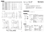
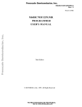
M68HC705BPGMR/D
October 1995
M68HC705BPGMR
PROGRAMMER
USER'S MANUAL
First Edition
© MOTOROLA Ltd., 1995; All Rights Reserved
Motorola reserves the right to make changes without further notice to any products herein to
improve reliability, function, or design. Motorola does not assume any liability arising out of
the application or use of any product or circuit described herein; neither does it convey any
license under its patent rights nor the rights of others. Motorola products are not designed,
intended, or authorized for use as components in systems intended for surgical implant into
the body, or other application in which the failure of the Motorola product could create a
situation where personal injury or death may occur. Should Buyer purchase or use Motorola
products for any such unintended or unauthorized application, Buyer shall indemnify and
hold Motorola and its officers, employees, subsidiaries, affiliates, and distributors harmless
against all claims, costs, damages, and expenses, and reasonable attorney fees arising out of,
directly or indirectly, any claim of personal injury or death associated with such unintended
or unauthorized use, even if such claim alleges that Motorola was negligent regarding the
design or manufacture of the part.
Motorola and the Motorola logo are registered trademarks of Motorola Inc.
Motorola Inc. is an Equal Opportunity/Affirmative Action Employer.
CONTENTS
TABLE OF CONTENTS
1. INTRODUCTION . . . . . . . . . . . . . . . . . . . . . . . . . . . . . . . . . . . . . . . . . . . . . . . . . . . . . . . . . . . . . . . . . . . . . . . . . . . . . . . . . . . . . . 1-1
1.1 BOARD LAYOUT AND DESCRIPTION ................................................................................... 1-2
1.2 PROGRAMMING MODES ...................................................................................................... 1-2
2. PARALLEL MODE . . . . . . . . . . . . . . . . . . . . . . . . . . . . . . . . . . . . . . . . . . . . . . . . . . . . . . . . . . . . . . . . . . . . . . . . . . . . . . . . . . . . 2-1
2.1 68HC805B6 PARALLEL PROGRAMMING MODE .................................................................... 2-1
2.1.1 Programming Procedure.................................................................................................... 2-1
2.1.2 Notes on the Programming Operation................................................................................... 2-1
2.2 68HC705B5 PARALLEL PROGRAMMING MODE .................................................................... 2-2
2.2.1 Programming Procedure.................................................................................................... 2-2
2.2.2 Notes on the Programming Operation................................................................................... 2-2
2.3 68HC705B16 PARALLEL PROGRAMMING MODE................................................................... 2-3
2.3.1 Programming Procedure.................................................................................................... 2-3
2.3.2 Notes on the Programming Operation................................................................................... 2-3
2.4 MCU BLANK CHECK (705B5/705B16 ONLY) .......................................................................... 2-4
2.4.1 Check Procedure .............................................................................................................. 2-4
2.4.2 Notes on the Blank Check Operation..................................................................................... 2-4
2.5 68HC705B32 PARALLEL PROGRAMMING MODE................................................................... 2-5
2.5.1 Programming Procedure.................................................................................................... 2-5
2.5.2 Notes on the Programming Operation................................................................................... 2-5
3. SERIAL MODE . . . . . . . . . . . . . . . . . . . . . . . . . . . . . . . . . . . . . . . . . . . . . . . . . . . . . . . . . . . . . . . . . . . . . . . . . . . . . . . . . . . . . . . . 3-1
3.1 MC68HC805B6 SERIAL PROGRAMMING MODE..................................................................... 3-1
3.1.1 Programming Procedure.................................................................................................... 3-1
3.1.2 Notes on the Serial Operation.............................................................................................. 3-1
3.2 MC68HC705B5 SERIAL PROGRAMMING MODE..................................................................... 3-2
3.2.1 Programming Procedure.................................................................................................... 3-2
3.2.2 Notes on the Serial Operation.............................................................................................. 3-2
3.3 XC68HC705B16 SERIAL PROGRAMMING MODE.................................................................... 3-4
3.3.1 Software Requirements ...................................................................................................... 3-4
3.3.2 Hardware Requirements..................................................................................................... 3-4
3.3.3 Programming Procedure.................................................................................................... 3-4
3.3.4 Notes on the Programming Operation................................................................................... 3-5
3.4 MC68HC705B32 SERIAL PROGRAMMING MODE................................................................... 3-6
3.4.1 Software Requirements ...................................................................................................... 3-6
3.4.2 Hardware Requirements..................................................................................................... 3-6
3.4.3 Programming Procedure.................................................................................................... 3-6
4. ADDITIONAL INFORMATION. . . . . . . . . . . . . . . . . . . . . . . . . . . . . . . . . . . . . . . . . . . . . . . . . . . . . . . . . . . . . . . . . . . . . . . 4-1
4.1 SERIAL PROGRAMMING CABLE .......................................................................................... 4-1
M68HC705BPGMR/D
iii
MOTOROLA
CONTENTS
This page intentionally left blank
M68HC705BPGMR/D
iv
MOTOROLA
INTRODUCTION
CHAPTER
1. INTRODUCTION
This user manual describes the procedure used to program and verify an
MC68HC705B5/16/32 or MC68HC805B6 MCU on the M68HC705BPGMR (PGMR). All
that is required to program an MCU is the PGMR and a +5 volt and a VPP dc power supply.
The PGMR provides programming for either a 56 pin shrink dual-in-line package (SDIP), or
52 pin plastic leaded chip carrier (PLCC) MCU device programming.
S1 controls power
to the MCU
Install power
leads at P1
S2 controls the
MCU RESET
P1
Jumper Headers
configure the PGMR
JP3
S1
S2
JP1 JP2
JP4
JP5
JP7
JP6
P2
SKT3
SKT1
SKT2
Connect serial
cable at P2
Install the 52PLCC
MCU in SKT2
OR
SKT1 contains
the program EPROM
Install the 56SDIP
MCU in SKT3
Figure 1.1 M68HC705BPGMR Layout
M68HC705BPGMR/D
1-1
MOTOROLA
INTRODUCTION
1.1 BOARD LAYOUT AND DESCRIPTION
Figure 1.1 shows the layout of the PGMR. As shown in the figure there are various controls,
connectors and sockets that provide the ability to configure the board to specific MCU
programming requirements.
There are two connectors on the board. For the board to function correctly you must supply
the required power to the board at connector P1. +5V dc @ 100mA and ground lines are
required. In addition a VPP power supply is needed to perform the programming. The value
of this supply may vary between MCUs, please refer to this manual and the device data book
for further information.
Connector P2 provides a serial programming capability. When using this mode, you must
connect a serial cable between P2 and your host computer. In this case you do not require to
install an EPROM in SKT1.
Switches S1 and S2 control the activity of the PGMR. S1 is a simple on/off switch that
applies power to the MCU device when on. Never remove or install an MCU when the S1
switch is in the ON position. S2 control the MCU reset line. Neither parallel or serial
programming can take place while the part is in reset mode.
Seven jumper headers (JP1 to JP7) configure the PGMR for the particular MCU and fucntion
in use. They select between different MCUs, programming modes (serial vs. parallel),
EPROM sizes, and modes. The following sections describe how to configure these jumpers
for your programming requirements.
Lastly, sockets SKT2 to SKT3 allow for the installation of the MCUs and, if required, the
master EPROM. SKT2 provides support for a 52 pin PLCC package and SKT32 for a 56 pin
SDIP package. Not all of the MCUs supported by this board may be available in each
package. The SKT2 socket requires that the MCU is installed in a top-down or dead-bug
fashion.
IMPORTANT NOTE
You must never install more than one MCU on this board at any time. That is
there must never be an MCU installed in SKT2 and another installed in SKT3
simultaneously. Such a configuration may damage either of the MCUs and
the board itself.
SKT1 provides a socket for the master EPROM used in parallel programming. You do not
require to install this EPROM when the serial mode is used.
Always ensure that the devices are orientated correctly into their respective sockets.
1.2 PROGRAMMING MODES
The PGMR supports two modes of programming. In parallel mode the user programs the
MCU by copying the contents of an EPROM in SKT1. See chapter 2 for instructions. In
serial mode the user communicates directly with the MCU via a serial cable and connector
P2. See Chapter 3 for instructions.
M68HC705BPGMR/D
1-2
MOTOROLA
PARALLEL MODE
CHAPTER
2. PARALLEL MODE
This programming mode copies a user program contained in an external EPROM, into the
internal PROM (OTPROM/EPROM) of the MC68HC705B MCU device (or EEPROM in the
case of the 805B6).
The following sections describe the procedure taken to program each MCU type.
2.1 68HC805B6 PARALLEL PROGRAMMING MODE
Settings required:
JP1
JP3
JP5
JP7
S2
805B6
MODE B
27C64/27C128
PARALLEL
IN
JP2
JP4
JP6
S1
SKT1
805B6
EPROM
27C64
OFF
27C64 EPROM Installed
2.1.1 Programming Procedure
a) Apply power to the PGMR board.
b) Insert the 805B6 MCU device into the PGMR.
c) Set S1 to ON.
d) Set S2 to OUT. The selected programming routine is then executed.
e) Once the programming is complete (see section 2.1.2), set S2 to IN and S1 to OFF. You
may now remove the MCU from the socket.
2.1.2 Notes on the Programming Operation
EEPROM6 is first erased then checked. If a non $FF byte is detected, the RED LED D3 will
be turned on, and erase will be performed a second time, and so on until total erasure. Before
proceeding to erase the EEPROM1 the RED LED D3 is turned off, then erasure of
EEPROM1 takes place in a similar fashion to the EEPROM6, thus clearing the security bit if
needed.
Next both EEPROMs are programmed in turn, in increasing address order from the external
EPROM. A ‘fast’ algorithm is used that skips over $FF bytes, thus speeding up the loading
process. During programming, the GREEN LED D2 will flash at about 3Hz (much faster if
DATA = $FF).
Upon completion of the programming operation, the EEPROM’s content will be checked
against the external EPROM. If the device verifies correctly, the GREEN LED D2 will stay
ON, else if an error is detected the RED LED D3 will turn ON (GREEN LED off).
M68HC705BPGMR/D
2-1
MOTOROLA
PARALLEL MODE
2.2 68HC705B5 PARALLEL PROGRAMMING MODE
Settings required:
JP1
JP3
JP5
JP7
S2
705B5/B16
MODE A
27C64/27C128
PARALLEL
IN
JP2
JP4
JP6
S1
SKT1
705B5/B16
EPROM
27C64
OFF
27C64 EPROM Installed
2.2.1 Programming Procedure
a) Apply power to the PGMR board.
b) Insert the 705B5 MCU device into the PGMR.
c) Set S1 to ON.
d) Set S2 to OUT. The selected programming routine is then executed.
e) Once the programming is complete (see section 2.2.2), set S2 to IN and S1 to OFF. You
may now remove the MCU from the socket.
2.2.2 Notes on the Programming Operation
During programming, the GREEN LED D2 will flash at about 3 Hz.
Upon completion of the programming operation, the internal EPROM content will be
checked against the external EPROM. If the device verifies correctly, the GREEN LED D2
will stay ON, else if an error is detected the RED LED D3 will turn ON (GREEN LED off).
M68HC705BPGMR/D
2-2
MOTOROLA
PARALLEL MODE
2.3 68HC705B16 PARALLEL PROGRAMMING MODE
Settings required:
JP1
JP3
JP5
JP7
S2
705B5/B16
MODE A
27C64/27C128
PARALLEL
IN
JP2
JP4
JP6
S1
SKT1
705B5/B16
EPROM
27C128
OFF
27C128 EPROM Installed
2.3.1 Programming Procedure
a) Apply power to the PGMR board.
b) Insert the 705B16 MCU device into the PGMR.
c) Set S1 to ON.
d) Set S2 to OUT. The selected programming routine is then executed.
e) Once the programming is complete (see section 2.3.2), set S2 to IN and S1 to OFF. You
may now remove the MCU from the socket.
2.3.2 Notes on the Programming Operation
The EPROM will first be verified as being blank. At the first byte not erased to $00, the RED
LED D3 will turned ON and the routine will stay in a loop. When the whole EPROM content
is checked as erased, the GREEN LED D2 will be turned ON.
The contents of EEPROM1 will then be erased. If a non $FF byte is detected, the RED LED
will be turned on, and erase will be performed a second time, and so on until total erasure.
After both the EPROM and the EEPROM1 are checked as erased and the security bit is
cleared. The programming operation can be performed.
All EPROM and EEPROM1 locations will be loaded, in increasing address order. Segments
containing no EPROM or EEPROM will be skipped by the loader.
During programming, the GREEN LED D3 will flash at about 3 Hz.
Upon completion of the program operation, the EPROM and EEPROM1 content will be
checked against the external EPROM. If the device verifies correctly, the GREEN LED D2
will stay ON, else if an error is detected the RED LED D3 will turn ON (GREEN LED off).
NOTE
Firmware errors in the silicon mask set C97K, prevent correct operation of the parallel mode.
If you are using this mask set then please use the serial mode instead.
M68HC705BPGMR/D
2-3
MOTOROLA
PARALLEL MODE
2.4 MCU BLANK CHECK (705B5/705B16 ONLY)
Settings required:
JP1
JP3
JP5
JP7
S2
705B5/705B16
MODEB
27C64/27C128
PARALLEL
IN
JP2
JP4
JP6
S1
SKT1
705B5/705B16
EPROM
27C64
OFF
EPROM NOT Installed
2.4.1 Check Procedure
a) Apply power to the PGMR board.
b) Insert the 705B5/16 MCU device into the PGMR.
c) Set S1 to ON.
d) Set S2 to OUT. The selected blank check routine is then executed.
e) Once the blank check is complete (see section 2.3.2), set S2 to IN and S1 to OFF. You
may now remove the MCU from the socket.
2.4.2 Notes on the Blank Check Operation
If the device is in the erased state the green LED will light, if the part is non blank the red
LED will light. An EPROM with $00 programmed into all locations may also be installed in
SKT1.
M68HC705BPGMR/D
2-4
MOTOROLA
PARALLEL MODE
2.5 68HC705B32 PARALLEL PROGRAMMING MODE
Settingrequired:
JP1
JP3
JP5
JP7
S1
SKT1
705B5/B16
MODE A
NC
PARALLEL
OFF
EPROM Installed
JP2
JP4
JP6
LK1
S2
705B5/B16
EPROM
27C128
connect to LK2
IN
2.5.1 Programming Procedure
a) Apply power to the PGMR board.
b) Insert the 705B32 MCU device into the PGMR.
c) Set S1 to ON.
d) Set S2 to OUT. The selected programming routine is then executed.
e) Once the programming is complete (see section 2.3.2), set S2 to IN and S1 to OFF. You
may now remove the MCU from the socket.
2.5.2 Notes on the Programming Operation
GREEN LED flashes signifying that programming is taking place.
M68HC705BPGMR/D
2-5
MOTOROLA
PARALLEL MODE
This page intentionally left blank
M68HC705BPGMR/D
2-6
MOTOROLA
SERIAL MODE
CHAPTER
3. SERIAL MODE
This programming mode allows the user to download an S-record format file directly into the MCU
by using an external computer system. The following sections describe the procedure taken to
program each MCU type.
3.1 MC68HC805B6 SERIAL PROGRAMMING MODE
Settings required:
JP1
JP3
JP5
JP7
S2
P2
805B6
MODE A
27C64/27C128
SERIAL
IN
Serial cable to PC
JP2
JP4
JP6
S1
SKT1
805B6
EPROM
27C64
OFF
EPROM NOT Installed
3.1.1 Programming Procedure
a) Apply power to the PGMR board.
b) Insert the 805B6 MCU device into the PGMR.
c) Set S1 to ON.
d) Set S2 to OUT. The selected serial routine is then executed.
3.1.2 Notes on the Serial Operation
The serial operation consists of two steps. Firstly, the EEPROM6 will first be erased then checked
for complete erasure; if a non $FF byte is detected, the RED LED D3 will be turned on, and erase
will be performed a second time, and so on until total erasure. Before proceeding to erase the
EEPROM1, the RED LED D3 is turned off, then erasure of EEPROM1 takes place in a similar
fashion, thus clearing the security bit if needed.
Secondly, control is given to the serial routine. The serial routine communicates through the SCI to
an external host, typically a PC, by means of an RS232 link at 9600 baud, 8 bit, no parity, full
duplex.
M68HC705BPGMR/D
3-1
MOTOROLA
SERIAL MODE
ATTENTION:
DATA format is not ASCII, but 8-bit binary, so a complementary program must be
run by the host to supply the required format. Such a program is available for the IBM
PC from MOTOROLA. The format accepted by the serial loader is as follows:
<address high> <address low> <data>
These three bytes must be sent by the host for each address to be programmed.
The protocol is as follows:
3.1.3 The MC68HC805B6 sends the last byte programmed to the host as a prompt (the first time,this
data is undermined), this allows verification by the host of proper programming.
3.1.4 In response to this prompt, the host sends the 3 bytes as outlined above.
3.1.5 If the data if different from $FF, it is programmed to the address provided, be it PORT, RAM
($50-$7C used by the loader - not available) or EEPROM.
3.1.6 Loop to 1.
If the data sent is $FF, programming does not take place (EEPROMs only), and the content of the
accessed location is actually returned as a prompt.
See 805B6 specification for further information.
3.2 MC68HC705B5 SERIAL PROGRAMMING MODE
Jumper settings required:
JP1
JP3
JP5
JP7
S2
P2
705B5/B16
MODE A
27C64/27C128
SERIAL
IN
Serial cable to PC
JP2
JP4
JP6
S1
SKT1
705B5/B16
RAM
27C64
OFF
EPROM NOT Installed
3.2.1 Programming Procedure
a) Apply power to the PGMR board.
b) Insert the 705B5 MCU device into the PGMR.
c) Set S1 to ON.
d) Set S2 to OUT. The selected serial routine is then executed.
3.2.2 Notes on the Serial Operation
The serial operation consists of two steps. Firstly, the EEPROM1 will first be erased then checked
for complete erasure; if a non $FF byte is detected, the RED LED D3 will be turned on, and erase
will be performed a second time, and so on until total erasure, thus clearing the security bit if needed.
M68HC705BPGMR/D
3-2
MOTOROLA
SERIAL MODE
Secondly, control is given to the serial routine. The serial routine communicates through the SCI to
an external host, typically a PC, by means of an RS232 link at 9600 baud, 8 bit, no parity, full
duplex.
ATTENTION:
DATA format is not ASCII, but 8-bit binary, so a complementary program must be
run by the host to supply the required format. Such a program is available for the IBM
PC from MOTOROLA. The format accepted by the serial loader is as follows:
<address high> <address low> <data0> <data1> <data2> <data3>
These six bytes must be sent by the host for each group of four address to be
programmed.
The protocol is as follows:
3.2.3 The MC68HC705B5 sends the last two bytes programmed to the host as a prompt, this allows
for verification by the host of proper programming. NOTE: After reset the MC68HC705B5 serial
bootstrap routine will first echo two blocks of 4 bytes at $00, as no data is programmed yet.
3.2.4 In response to the first byte prompt, the host sends the first address byte.
3.3.5 After receiving the first address byte, the MC68HC705B5 sends the next byte programmed.
3.3.6 The exchange of data continues until the MC68HC705B5 has sent the four data bytes, and the
host has sent 2 address bytes and 4 data bytes.
3.3.7 If the data is different from $00, it is programmed, at the address provided, while the next
address and bytes are received and the previous data is echoed.
3.3.8 Loop to 1.
If the data sent in is $00, no programming in the EPROM takes place, and the content of the accessed
location is returned as a prompt. The entire EPROM memory can be read in this fashion. The RED
LED D3 will be on is the data read is not $00.
During programming, the GREEN LED D2 will flash.
M68HC705BPGMR/D
3-3
MOTOROLA
SERIAL MODE
3.3 XC68HC705B16 SERIAL PROGRAMMING MODE
Settings required:
JP1
JP3
JP5
JP7
S2
P2
705B5/B16
MODE A
27C64/27C128
SERIAL
IN
Serial cable to PC
JP2
JP4
JP6
S1
SKT1
705B5/B16
RAM
27C128
OFF
EPROM NOT Installed
3.3.1 Software Requirements
EPB16.EXE Revision C.0.
NOTE:
EPB16 programs only allows for the programming and verification of 705B16 (and
705X16) parts - it cannot be used on 705B5 or 805B6 parts.
3.3.2 Hardware Requirements
The hardware requirements to run the EPB16 program are as follows:
1 x IBM® PC Compatible Personal Computer
1 x Serial Port (must be communication port 1 - COM1)
1 x Connecting Cable
3.3.3 Programming Procedure
a) Apply power to the PGMR board.
b) Insert the 70B16 MCU device into the PGMR.
c) Set S1 to ON.
d) Set S2 to OUT.
e) Execute the EPB16 program as follows:
EPB16 [-xxx] [program.ext] <return>
-xxx is a special delay modifier that allows the program to operate correctly on fast computers. Use 2 for a 386 @ 25Mhz.
program.ext is the full name of the file containing the S-record data to program the EPROM and
EEPROM. The S-record file must contain data only at EPROM or EEPROM locations.
Downloading data into registers or into RAM will disturb the correct serial operation.
f) If a file name was not specified when invoking EPB16 program, the "F" command must be
executed.
g) Enter "D" to download the file data to the MCU. As the data is downloaded the EPROM and/or
EEPROM of the MCU is programmed. The "D" command only operates when an S-record file is
loaded.
M68HC705BPGMR/D
3-4
MOTOROLA
SERIAL MODE
NOTE
The download process is automatically followed by a verification process which
compares the bytes sent to the MCU with those echoed by the MCU. Differences, if
any, are reported in the following format: Addr Sent Recv; where Addr is the
location which was sent the value Sent, and Recv is the value which was echoed. The
three values are in hexadecimal.
h) Enter “V” to verify the MCU memory contents. The "S" command is used to show the MCU
memory contents.
i) Once the programming is complete, set S2 to IN and S1 to OFF. You may now remove the MCU
from the socket.
j) Quit EPB16 using either the "X" or "Q" command.
3.3.4 Notes on the Programming Operation
The serial bootstrap routine communicates through the SCI to an external host, typically a PC, by
means of an RS232 link at 9600 baud, 8 bit, no parity, full duplex.
M68HC705BPGMR/D
3-5
MOTOROLA
SERIAL MODE
3.4 MC68HC705B32 SERIAL PROGRAMMING MODE
Settings required:
JP1
JP3
JP5
JP7
S1
SKT1
705B5/B16
MODE A
NC x
SERIAL
OFF
EPROM NOT Installed
JP2
JP4
JP6
LK1
S2
P2
705B5/B16
RAM
27C128
connect to LK2.
IN
Serial cable to PC
3.4.1 Software Requirements
EPBX32.EXE Revision 0.3.
3.4.2 Hardware Requirements
The hardware requirements to run the EPBX32 program are as follows:
1 x IBM® PC Compatible Personal Computer
1 x Serial Port (COM1 or COM2)
1 x Connecting Cable (see diagrams at end of errata)
3.4.3 Programming Procedure
a) Apply power to the PGMR board.
b) Insert the 70B32 MCU device into the PGMR.
c) Set S1 to ON.
d) Set S2 to OUT.
e) Execute the EPBX32 program as follows:
EPBX32 [com] <return>
comm is an optional comms port setting. The default is COM1.
f) Follow the instructions on the PC screen.
NOTE
The download S-record file must be in Motorola EXORCISOR format. The S-record
file must only contain data at EPROM or EEPROM locations. Downloading data into
registers or into RAM can disturb the correct serial operation.
g) Once the programming is complete, set S2 to IN and S1 to OFF. You may now remove the MCU
from the socket.
j) Quit EPBX32 using either the "X" or "Q" command.
M68HC705BPGMR/D
3-6
MOTOROLA
ADDITIONAL INFORMATION
CHAPTER
4. ADDITIONAL INFORMATION
4.1 SERIAL PROGRAMMING CABLE
Figure 4-1. shows a PGMR/Host Computer Cable Assembly Diagram. If a nine way
connector is used the signals must be mapped correctly.
20 OR 25 CONDUCTOR
FLAT RIBBON
CABLE
3M #3365-20
OR
3M #3365-25
25 "D" SUBMINIATURE
MALE(PIN)
CONNECTORPART #'S:
25 "D" SUBMINIATURE
FEMALE(SOCKET)
CONNECTORPART #'S:
1. CIRCUIT ASSEMBLY CORP
#CA•25•SMD•P
1. CIRCUIT ASSEMBLY CORP
#CA•25•SMD•S
2. ITT CANNON #DBSP-B25P
2. ITT CANNON #DBSP-B25S
3. ANSLEY #609•25P
3. ANSLEY #609•25S
4. WINCHESTER #49•1125P
4. WINCHESTER #49•1125S
25 PIN "D" SUBMINIATURE CONNECTOR
1
2
14
3
15
4
16
5
17
6
18
7
19
8
20
9
10
21
22
11
23
12
24
13
25
1
2
14
3
15
4
16
5
17
6
18
7
19
DCD
NOT CONNECTED
DTR
SIGNAL GND
DSR
CTS
RTS
RXD
GND
TXD
RED WIRE
8
20
9
21
10
22
11
23
12
24
13
25
25 PIN "D" SUBMINIATURE CONNECTOR
M68HC705BPGMR/D
4-1
MOTOROLA
ADDITIONAL INFORMATION
A Hayes compatible modem cable, purchased from a local computer store, can be used to
connect the PGMR to the host computer.
The PGMR is wired as data communication equipment (DCE) whereas a terminal and most
serial modem ports on host computers are wired as data terminal equipment (DTE). This lets
a straight-through cable be used for most setups.
If a different type of cable is used to connect the PGMR to the host computer, a null modem
adapter (shown below) may be required to match the cable to the EVS terminal port
connector.
A null modem adapter reverses the roles of various data and control signals to make a DTE
device appear as a DCE device, or vice versa.
DB-25S
DB-25P
GND
1
1
GND
TXD
2
2
TXD
RXD
3
3
RXD
RTS
4
4
RTS
CTS
5
5
CTS
DSR
6
6
DSR
SIG-GND
7
7
SIG-GND
DCD
8
8
DCD
DTR
20
20
DTR
FIGURE 4-2 Null Modem Adapter
M68HC705BPGMR/D
4-2
MOTOROLA