1
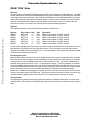
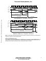
Freescale Semiconductor
Order this document by
MC68322UMAD/AD
MC68322
Addendum to
Freescale Semiconductor, Inc...
MC68322 Integrated Printer Processor
User’s Manual (Rev. 1.0)
This addendum to the initial release of the MC68322 UM/AD User’s Manual provides additional information
not included in the original text. This document and other information on this product is maintained on the
AESOP BBS, which can be reached at (800) 843-3451 (from the U.S. and Canada) or (512) 891-3650.
Configure modem for up to 14.4 Kbaud, 8 bits, 1 stop bit, and no parity. Terminal software should support
VT100 emulation. Internet access is provided by telneting to pirs.aus.sps.mot.com [129.38.233.1] or through
the World Wide Web at http://pirs.aus.sps.mot.com.
Mask Set G59B
Enhanced Functionality
Mask Set G59B of the MC68322 integrated printer processor provides a greater level of enabling technology
for the development of low-cost printing solutions. To eliminate some of the external circuitry normally
required on a printer controller board, Mask Set G59B lets users reprogram some of the least frequently used
pins as I/O pins. Additionally, to reduce the overall DRAM requirements of a printer controller, a new timing
mode is available in the MC68322 DRAM controller that will allow font ROMs to easily attach to any of the
DRAM channels. These enhancements have supplemented the high level of functionality provided by the
original MC68322 in a nonintrusive manner. Because the pinout and default behavior is identical to that of
the original MC68322, G59B devices can be used in controller boards designed for the original MC68322
without any hardware modifications. If the enhanced functionality is not required, existing MC68322 software
will not require modification, provided that it was written so that a zero is always assigned to any unused
control register bits (refer to Appendix C of the MC68322 User’s Manual).
Alternate Pin Functions
Overview
This is a description of the MC68322 alternate pin functions available in Mask Set G59B. In small systems
where many of the pins are not used, these pins may be individually programmed as general-purpose inputs
and outputs, thereby providing as many as 4 I/O pins, 12 output pins, and 2 interrupt/input pins.
Pins
The following 18 pins have alternate functions. Each of these pins powers up with their normal function.
Software written for previous revisions of the MC68322 will operate identically on Mask Set G59B provided
users write zeroes to all unused register bits, as defined by Appendix C of the MC68322 User's Manual. To
alternately define these pins, software may program the ALTPIN SEL register to assign an alternate function
to each pin. The following table shows the pins and the pin type when the ALTPIN SEL register bit is set.
Note that three of the alternate bus master output signals share a register bit.
© Freescale Semiconductor, Inc., 2004. All rights reserved.
1996 Motorola, Inc. All Rights Reserved.
Freescale Semiconductor, Inc...
Freescale Semiconductor, Inc.
PIN
PIN TYPE
ALTPIN SEL =1
A (22)
A (23)
A(24)
A(25)
A (21)
CS* (4)
CS* (5)
CS* (6)
CS* (7)
RAS* (4)
RAS* (5)
WRU*
DACK*
AS*
DTACK*
BG*
BR*
DREQ*
Input / Output
Input / Output
Input / Output
Input / Output
Output
Output
Output
Output
Output
Output
Output
Output
Output
Output
Output
Output / Buzzer
Input / Interrupt
Input / Interrupt
00FFF910
ALTPIN SEL
Register Bit
0
1
2
3
4
5
6
7
8
9
10
11
12
13
13
13
14
15
00FFF912
ALTPIN DIR
Register Bit
0
1
2
3
-
00FFF914
ALTPIN IN
Register Bit
0
1
2
3
-
00FFF916
ALTPIN OUT
Register Bit
0
1
2
3
4
5
6
7
8
9
10
11
12
13
14
-
State During Reset
The output pins are in the normal de-asserted state during reset and the first bus cycles, except for A(21:25),
AS*, and RAS*(4:5). Pins A(22:25) may be used as inputs on systems that require 4 Mbyte or less of ROM
by using the Input Pin mode as described below.
Registers
The following new registers control the alternate pin function:
Register
ALTPIN SEL
ALTPIN DIR
ALTPIN IN
ALTPIN OUT
Reg. Address
00FFF910
00FFF912
00FFF914
00FFF916
Bits
16
4
4
15
R/W
R/W
R/W
R
R/W
Description
Select alternate function for each pin
Direction control for A(22:25), 0=in, 1=out
Input status for A(22:25)
Output control for output bits
The following bits have been added to the existing external interrupt registers: The DREQ* (EXIR2) bits are
added to the EXIR0 registers; the BR* (EXIR3) bits are added to the EXIR1 registers. The new bits are located
immediately adjacent to the bits already contained in those registers. For example, the EXIR0 enable bit is bit
0 in the EXIR0 ENB register and the EXIR2 enable bit will be bit 1. Similarly, the EXIR0 status and request
bits are bit 1 and bit 0 of the EXIR0 EVENT register, respectively, and the EXIR2 status and request bits will
be bit 3 and bit 2, respectively. EXIR0 and EXIR2 will share the same interrupt level as will EXIR1 and EXIR3.
If BR* or DREQ* are to be used as simple inputs rather than interrupts, then software should keep the
interrupts disabled. Users can check the input pin status by reading the status bit for the corresponding pin
in the appropriate external interrupt event register. In a similar way, the IRQ0 and IRQ1 pins have always
been available as input pins.
2
MC68322 USER MANUAL ADDENDUM
For More Information On This Product,
Go to: www.freescale.com
Freescale Semiconductor, Inc.
Register
EXIR0 ENB
EXIR0 EVENT
EXIR0 MODE
EXIR0 SEN
EXIR1 ENB
EXIR1 EVENT
EXIR1 MODE
EXIR1 SEN
Reg. Address
00FFF770
00FFF772
00FFF776
00FFF778
00FFF780
00FFF782
00FFF786
00FFF788
Bits
1
2
2
1
1
2
2
1
R/W
R/W
R/W
R/W
R/W
R/W
R/W
R/W
R/W
Description
Interrupt EXIR2 Enable
Interrupt EXIR2 Request and Status
Interrupt EXIR2 Mode
Interrupt EXIR2 Software Enable Bit
Interrupt EXIR3 Enable
Interrupt EXIR3 Request and Status
Interrupt EXIR3 Mode
Interrupt EXIR3 Software Enable Bit
The following registers have been added for buzzer control:
Freescale Semiconductor, Inc...
Register
Reg. Address Bits
BUZZER INT 00FFF608
8
BUZZER ENB 00FFF60A
1
R/W
R/W
R/W
Description
Buzzer Interval
Buzzer Enable
Input Pin Mode
For A(22:25) to be programmed as input pins, they must be three-stated on power-up to prevent the processor
from driving them during the initial bus cycles, which could cause bus contention on these lines. To
accommodate this condition, A(22:25) will power-up in a three-state mode when a special state of the HIZ*
and TEST pins exists. The normal functions for BR* and DREQ* will also be disabled in Input Pin mode (note
ALTPIN SEL register bits 14,15 are set). The list below shows the modes for these pins.
HIZ*
0
0
TEST
0
1
1
0
1
1
Function
Three-state all outputs
Input Pin mode, A(22:25) tri-stated
ALTPIN SEL Register bits 0-3,14,15 = 1
Normal mode, A(22:25) enabled
ALTPIN SEL Register bits 0-15 = 0
Special test mode (do not use)
Buzzer
The BG* output pin now has a buzzer control function, which consists of an 8-bit interval control register, a 1bit enable register, and a 16-bit free-running counter. The 8 bits in the BUZZER INT register control the value
to be loaded into the upper byte of the 16-bit counter after it reaches a count of zero. The lower byte will
always be loaded with $FF. The enable bit in the BUZZER ENB register causes the output from the BG* pin
to toggle every time the counter reaches zero. The buzzer function drives a buzzer on the board or front panel.
On products that need this feature, the buzzer control function saves a 555 chip with its resistors and
capacitors.
In-Circuit Emulation (ICE)
If the alternate pin function is to be used in a system, then an in-circuit emulator (ICE) cannot be used for
system development. This feature of the G59B Mask Set is not available in an ICE version. If the alternate
pin function will not be used in the system, then the original ICE version of the MC68322 can be used with an
in-circuit emulator.
Operational Example
If the alternate pin functions will not be used or if none of them will be be used as inputs, then HIZ* should be
connected to Vcc, and TEST (pin 159 of the PQFP package) should be connected to ground. If some of the
input pins will be used, then the Input Pin mode should be selected by connecting HIZ* to ground, and TEST
to Vcc. This connection powers up the A(22:25) pins to function as input pins and disables the normal BR*
and DREQ* input pin functions. Software would (1) load the ALTPIN OUT register with the initial values, (2)
load the ALTPIN DIR register to control the configuration of the A(22:25) pins, and then (3) load the ALTPIN
SEL register to control the pin configurations.
MC68322 USER’S MANUAL ADDENDUM
For More Information On This Product,
Go to: www.freescale.com
3
Freescale Semiconductor, Inc.
DRAM ‘‘ROM’’ Mode
Overview
This description is of the MC68322 DRAM controller ‘‘ROM mode’’ available in the G59B Mask Set. The ROM
mode of operation will cause the selected DRAM channel to run with extended cycle times while the remainder
of the channels operate at full speed. This will place font ROMs on one of the DRAM channels with only an
external latch required to demultiplex the address signals. By placing the font ROMs on one of the DRAM
channels, the MC68322 RISC graphics processor (RGP) will have direct access to font data, which will
eliminate the need for a font cache, thus reducing overall system DRAM requirements.
Freescale Semiconductor, Inc...
Registers
The registers listed below contain the bits used to activate the ROM mode.
Register
DRAM0
DRAM1
DRAM2
DRAM3
DRAM4
DRAM5
Reg. Address
00FFF100
00FFF110
00FFF120
00FFF130
00FFF140
00FFF150
Bits
12
12
12
12
12
12
R/W
R/W
R/W
R/W
R/W
R/W
R/W
Description
DRAM control register for RAS0* channel
DRAM control register for RAS1* channel
DRAM control register for RAS2* channel
DRAM control register for RAS3* channel
DRAM control register for RAS4* channel
DRAM control register for RAS5* channel
In each of these registers, bits 0-10 existed in the original version of the MC68322 and controlled the size and
base address of the DRAM block for the specified channel. The functionality of these bits has not been
changed in the G59B version of the MC68322. Bit 11 has been added to each register and activates the ROM
mode for the specified channel when set.
Functional Description
When the ROM mode is selected for one of the DRAM channels, the accesses to that channel are extended.
Each initial access and each burst access is extended by one CLK1 period (two CLK2 periods). For example,
in timing mode 1 the normal DRAM access time in CLK1s would be 4:2:2:2...; but when the ROM mode is
selected, the access time becomes 5:3:3:3... for that particular channel. This timing relaxation in the ROM
mode allows ROMs (which typically have longer access times than DRAM) to operate effectively on one (or
more) of the DRAM channels. At the same time, the other channels in the normal mode will run at full speed,
thereby achieving maximum use of the available bandwidth in the DRAMs and maximizing system
performance. In addition to extending the accesses, one CLK1 of idle time is inserted at the end of the entire
access to the channel when in the ROM mode. This idle clock allows the data bus to return to a state of high
impedance because ROMs can drive the data bus for an extended period of time after an access.
Timing Example
The following timing diagrams illustrate the difference between the DRAM accesses when in normal mode
and ROM mode. This example is for DRAM timing mode1 but similar behavior is exhibited in timing modes 0
and 2.
4
MC68322 USER MANUAL ADDENDUM
For More Information On This Product,
Go to: www.freescale.com
Freescale Semiconductor, Inc.
CLK2
MA10-0
ROW
COLUMN
COLUMN
ROW
COLUMN
RAS5-0
CAS1-0
DATA
MD15-0
SINGLE CYCLE
DATA
FAST PAGE CYCLE
Freescale Semiconductor, Inc...
INITIAL ACCESS
NEXT ACCESS...
Normal DRAM Access - Timing Mode 1 (Read Cycle)
CLK2
MA10-0
ROW
COLUMN
COLUMN
RAS5-0
CAS1-0
DATA
MD15-0
SINGLE CYCLE
DATA
FAST PAGE CYCLE
INITIAL ACCESS
IDLE
NEXT...
‘‘ROM Mode’’ DRAM Access - Timing Mode 1 (Read Cycle)
Note: The IDLE state shown here will also occur at the end of a refresh cycle whenever the ROM mode is
selected for at least one of the DRAM channels.
Address Demultiplexing Circuit
The MC68322 multiplexes the addresses on the DRAM bus as is required by standard DRAM devices. To
connect ROM to one of the DRAM channels, a simple address demultiplexing circuit must be used. The
following circuit provides an example of how to implement this logic in a system.
MC68322 USER’S MANUAL ADDENDUM
For More Information On This Product,
Go to: www.freescale.com
5
Freescale Semiconductor, Inc.
2 MBYTE DRAM --> ROM CIRCUIT
TO SECOND ROM
512K X 16
(OPTIONAL)
CE1*
RAS5*
74F00
LMA(9)
CE0*
LATCH
MA(9:0)
LMA(8:0)
68322
MD(15:0)
74ALS821
Freescale Semiconductor, Inc...
MA(9:0)
ROM 512K X 16
THE CIRCUIT FOR THE 74F00 SHOULD BE AS FOLLOWS:
SIGNALS
MA(9)
LMA(8:0)
MA(8:0)
ROM ADDRESS PINS
A(18)
A(17:9)
A(8:0)
LATCH
RAS5*
CE1*
LMA(9)
CE0*
Operational Example
A typical MC68322-based system might be a 16 MHz design that uses 70 ns DRAMs. To achieve maximum
system performance in this case, select DRAM timing mode 2. This system might also include 120 ns font
ROMs that could be attached to one of the DRAM channels using a circuit such as the one illustrated above.
Such an arrangement would minimize system cost by reducing the overall DRAM requirements. If the ROM
mode was not used, the system would need to be slowed to timing mode 0 to accommodate these font ROMs.
This slowdown would still produce a functional system but overall performance would be hindered because
this setup would not fully utilize the available bandwidth in the DRAMs. Instead, users should select timing
mode 2 for this system and should activate the ROM mode for the DRAM channel supporting the font ROMs.
These actions will optimize system performance as well as support the DRAM- based font ROMs that help
reduce system costs.
Chip–Select Timing
Pages 14-4 and 14-5 of the MC68322 User’s Manual timing diagrams show EC000 core reads and writes.
The timing diagrams that follow are provided for clarification. Figures 1 through 3 illustrate combinations of
chip-select parameters that produce zero wait-state reads on the EC000 bus. Figure 1 is similar to Figure 143 on page 14-4 of the user's manual. Figures 4 through 8 illustrate combinations of chip-select parameters
that produce one wait-state reads on the EC000 bus. Figure 9 illustrates the only combination of chip-select
parameters that produce zero wait-state writes on the EC000 bus. Figures 10 through 12 illustrate
combinations of chip-select parameters that produce one wait-state writes on the EC000 bus. The access
times for each timing diagram are shown in parentheses in CLK2s. The numbers within the parentheses are
defined as follows:
6
MC68322 USER MANUAL ADDENDUM
For More Information On This Product,
Go to: www.freescale.com
Freescale Semiconductor, Inc.
(SETUP:ACCESS:HOLD:RECOVER)
Freescale Semiconductor, Inc...
The SETUP value indicates the number of CLK2s between the assertion of the chip-select and the assertion
of RD or WR(U,L). The ACCESS value indicates the number of CLK2s that the RD or WR(U,L) signal will
remain asserted. The HOLD value indicates the number of CLK2s between the negation of RD or WR(U,L)
and the negation of the chip-select. Note that some of the access times are flagged with an asterisk (*)
because the access has a hold time of -1 CLK2s. This situation occurs whenever the "hold" value in one of
the chip-select registers is set to zero. In this case, the chip-select actually negates one CLK2 before the RD
or WR(U,L). This is important because for reads in such cases, the data must be set up to the negation of the
chip-select rather than the negation of the RD signal. The RECOVER value indicates the number of CLK2s
between the negation and reassertion of the chip-select (chip-select high time.) These timing diagrams are all
shown without extra recovery clocks (see page 6-3 of the user's manual), so the recovery time for each of the
cycles will be 3 CLK2s. To calculate the total cycle time, add the values in the parentheses. For example, the
first timing diagram (Fig. 1) shows an access time of (2:2:1:3). The total cycle time for this setup will be 8
CLK2s or 4 CLK1s, which is a zero wait-state access for the EC000 core.
S0
S1
S2
S3
S4
S5
S6
S7
S0
S1
S2
S3
CLK2
8
9
A25-1
9
14
14
CS7-0
16
16
RD
13
D15-0
12
WAIT
18
17
18
AS
18
R/W
EC000 Core Read Cycle AC Timing
Zero Wait State Access
RSET=0; RACC=0; RHLD=1
Figure 1. Read Access (2:2:1:3)
MC68322 USER’S MANUAL ADDENDUM
For More Information On This Product,
Go to: www.freescale.com
7
Freescale Semiconductor, Inc.
S0
S1
S2
S3
S4
S5
S6
S7
S0
S1
S2
S3
CLK2
8
9
A25-1
14
9
14
CS7-0
16
16
RD
13a
D15-0
12
WAIT
Freescale Semiconductor, Inc...
18
17
18
AS
18
R/W
EC000 Core Read Cycle AC Timing
Zero Wait State Access
RSET=0; RACC=1; RHLD=0
Figure 2. Read Access (2:4:-1:3)*
S0
S1
S2
S3
S4
S5
S6
S7
S0
S1
CLK2
8
9
A25-1
9
14
14
CS7-0
16
16
RD
13a
D15-0
12
WAIT
18
17
18
AS
18
R/W
EC000 Core Read Cycle AC Timing
Zero Wait State Access
RSET=1; RACC=0; RHLD=0
Figure 3. Read Access (4:2:-1:3)*
* hold time of -1 CLK2s (i.e. the chip select negates before the RD)
8
MC68322 USER MANUAL ADDENDUM
For More Information On This Product,
Go to: www.freescale.com
S2
S3
Freescale Semiconductor, Inc.
S0
S1
S2
S3
S4
W
W
S5
S6
S7
S0
S1
S0
S1
CLK2
8
9
A25-1
14
9
14
CS7-0
16
16
RD
D15-0
12
WAIT
Freescale Semiconductor, Inc...
18
17
18
AS
18
R/W
EC000 Core Read Cycle AC13Timing
One Wait State Access
RSET=0; RACC=0; RHLD=2
Figure 4. Read Access (2:2:3:3)
S0
S1
S2
S3
S4
W
W
S5
S6
S7
CLK2
8
9
A25-1
9
14
14
CS7-0
16
16
RD
13
D15-0
12
WAIT
18
17
18
AS
18
R/W
EC000 Core Read Cycle AC Timing
One Wait State Access
RSET=0; RACC=1; RHLD=1
Figure 5. Read Access (2:4:1:3)
MC68322 USER’S MANUAL ADDENDUM
For More Information On This Product,
Go to: www.freescale.com
9
Freescale Semiconductor, Inc.
S0
S1
S2
S3
S4
W
W
S5
S6
S7
S0
S1
CLK2
8
9
A25-1
14
9
14
CS7-0
16
16
RD
13
D15-0
12
WAIT
Freescale Semiconductor, Inc...
18
17
18
AS
18
R/W
EC000 Core Read Cycle AC Timing
One Wait State Access
RSET=1; RACC=0; RHLD=1
Figure 6. Read Access (4:2:1:3)
S0
S1
S2
S3
S4
W
W
S5
S6
S7
S0
CLK2
8
9
A25-1
9
14
14
CS7-0
16
16
RD
13a
D15-0
12
WAIT
18
17
18
AS
18
R/W
EC000 Core Read Cycle AC Timing
One Wait State Access
RSET=0; RACC=2; RHLD=0
Figure 7. Read Access (2:6:-1:3)*
* hold time of -1 CLK2s (i.e. the chip select negates before the RD)
10
MC68322 USER MANUAL ADDENDUM
For More Information On This Product,
Go to: www.freescale.com
S1
Freescale Semiconductor, Inc.
S0
S1
S2
S3
S4
W
W
S5
S6
S7
S0
S1
CLK2
8
9
A25-1
14
9
14
CS7-0
16
16
RD
13a
D15-0
12
Freescale Semiconductor, Inc...
WAIT
18
17
18
AS
18
R/W
EC000 Core Read Cycle AC Timing
One Wait State Access
RSET=1; RACC=1; RHLD=0
Figure 8. Read Access (4:4:-1:3)*
S0
S1
S2
S3
S4
W
W
S5
S6
S7
S0
S1
CLK2
8
9
A25-1
9
14
14
CS7-0
16
16
RD
13a
D15-0
12
WAIT
18
17
18
AS
18
R/W
EC000 Core Read Cycle AC Timing
One Wait State Access
RSET=2; RACC=0; RHLD=0
Figure 9. Read Access (6:2:-1:3)*
* hold time of -1 CLK2s (i.e. the chip select negates before the RD)
MC68322 USER’S MANUAL ADDENDUM
For More Information On This Product,
Go to: www.freescale.com
11
Freescale Semiconductor, Inc.
S0
S1
S2
S3
S4
S5
S6
S7
S0
S1
S2
S3
CLK2
8
9
A25-1
14
9
14
CS7-0
16
16
WR[U,L]
10
11
D15-0
WAIT
Freescale Semiconductor, Inc...
18
17
18
AS
18
R/W
EC000 Core Write Cycle AC Timing
Zero Wait State Access
WSET=1; WACC=0; WHLD=0
Figure 10. Write Access (4:2:-1:3)*
S0
S1
S2
S3
S4
W
W
S5
S6
S7
S0
CLK2
8
9
A25-1
9
14
14
CS7-0
16
16
WR[U,L]
10
11
D15-0
WAIT
18
17
18
AS
18
R/W
EC000 Core Write Cycle AC Timing
One Wait State Access
WSET=1; WACC=0; WHLD=1
Figure 11. Write Access (4:2:1:3)
* hold time of -1 CLK2s (i.e. the chip select negates before the RD or WR[U,L])
12
MC68322 USER MANUAL ADDENDUM
For More Information On This Product,
Go to: www.freescale.com
S1
Freescale Semiconductor, Inc.
S0
S1
S2
S3
S4
W
W
S5
S6
S7
S0
S1
CLK2
8
9
A25-1
9
14
14
CS7-0
16
16
WR[U,L]
10
11
D15-0
Freescale Semiconductor, Inc...
WAIT
18
17
18
AS
18
R/W
EC000 Core Write Cycle AC Timing
One Wait State Access
WSET=1; WACC=1; WHLD=0
Figure 12. Write Access (4:4:-1:3)*
* hold time of -1 CLK2s (i.e. the chip select negates before the WR[U,L])
MC68322 USER’S MANUAL ADDENDUM
For More Information On This Product,
Go to: www.freescale.com
13
Freescale Semiconductor, Inc.
S0
S1
S2
S3
S4
W
W
S5
S6
S7
S0
CLK2
8
9
A25-1
9
14
14
CS7-0
16
16
WR[U,L]
10
11
D15-0
Freescale Semiconductor, Inc...
WAIT
18
17
18
AS
18
R/W
EC000 Core Write Cycle AC Timing
One Wait State Access
WSET=2; WACC=0; WHLD=0
Figure 13. Write Access (6:2:-1:3)*
* hold time of -1 CLK2s (i.e. the chip select negates before the WR[U,L])
Information in this document is provided solely to enable system and software
implementers to use Freescale Semiconductor products. There are no express or
implied copyright licenses granted hereunder to design or fabricate any integrated
circuits or integrated circuits based on the information in this document.
Freescale Semiconductor reserves the right to make changes without further notice to
any products herein. Freescale Semiconductor makes no warranty, representation or
guarantee regarding the suitability of its products for any particular purpose, nor does
Freescale Semiconductor assume any liability arising out of the application or use of
any product or circuit, and specifically disclaims any and all liability, including without
limitation consequential or incidental damages. “Typical” parameters which may be
provided in Freescale Semiconductor data sheets and/or specifications can and do
vary in different applications and actual performance may vary over time. All operating
parameters, including “Typicals” must be validated for each customer application by
customer’s technical experts. Freescale Semiconductor does not convey any license
under its patent rights nor the rights of others. Freescale Semiconductor products are
not designed, intended, or authorized for use as components in systems intended for
surgical implant into the body, or other applications intended to support or sustain life,
or for any other application in which the failure of the Freescale Semiconductor product
could create a situation where personal injury or death may occur. Should Buyer
purchase or use Freescale Semiconductor products for any such unintended or
unauthorized application, Buyer shall indemnify and hold Freescale Semiconductor
and its officers, employees, subsidiaries, affiliates, and distributors harmless against all
claims, costs, damages, and expenses, and reasonable attorney fees arising out of,
directly or indirectly, any claim of personal injury or death associated with such
unintended or unauthorized use, even if such claim alleges that Freescale
Semiconductor was negligent regarding the design or manufacture of the part.
S1