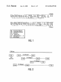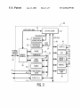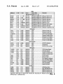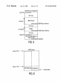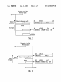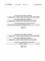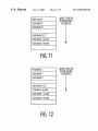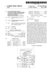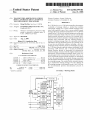
1
US006510479B1
(12) United States Patent
(10) Patent N0.:
(45) Date of Patent:
Ha0
US 6,510,479 B1
Jan. 21, 2003
Primary Examiner—Sumati LefkoWitZ
Assistant Examiner—Christopher E. Lee
(54) TRANSMIT PRE-ARBITRATION SCHEME
FOR A CAN DEVICE AND A CAN DEVICE
THAT IMPLEMENTS THIS SCHEME
(57)
ABSTRACT
(75) Inventor: Hong Bin Hao, San Jose, CA (US)
In a CAN device, e.g., a CAN microcontroller, that supports
a plurality of message objects, a method that includes
(73) Assignee: Koninklijke Philips Electronics N.V.,
Eindhoven (NL)
(*)
Notice:
concurrently staging tWo or more transmit messages asso
ciated With respective ones of tWo or more enabled transmit
Subject to any disclaimer, the term of this
patent is extended or adjusted under 35
message objects for attempted transmission over a CAN bus
coupled to the CAN device, and performing a pre-arbitration
USC 154(b) by 255 days.
process to determine Which of the tWo or more concurrently
staged transmit messages has priority. The message deter
(21) Appl. No.: 09/630,642
(22) Filed:
Aug. 1, 2000
mined to have priority is deemed a Winning message and the
message object associated With the Winning message is
deemed a Winning message object. In a presently preferred
Related US. Application Data
(60)
embodiment, the pre-arbitration process is a selected one of
at least tWo pre-arbitration schemes, including a ?rst pre
Provisional application No. 60/154,022, ?led on Sep. 15,
1999.
(51)
Int. Cl.7 .............................................. .. G06F 13/14
(52)
(58)
US. Cl. ...................... .. 710/240; 710/116; 710/305
Field of Search ....................... .. 709/229; 713/502;
arbitration scheme Whereby priority is determined according
to a CAN bus arbitration priority scheme established by the
governing CAN protocol, and a second pre-arbitration
scheme Whereby priority is determined by selecting the
370/300; 700/1, 23; 710/240, 116, 305
(56)
transmit message associated With the highest-numbered (or,
alternatively, lowest-numbered) message object as the Win
References Cited
ning message. In the event that more than one of the tWo or
U.S. PATENT DOCUMENTS
5,179,708 A
5,323,385 A
5’506’966 A
*
more concurrently staged transmit messages are determined
1/1993 Gyllstfom et a1~ ~~~~~~~~ ~~ 395/725
6/1994 Jurewlcz et a1‘ "
370/300
to have the same priority, the transmit message associated
With the highest-numbered message object is designated as
4/1996 Ban """""" "
the Winnin messa e The method further includes attem t
'
6,304,908 B1 * 10/2001
.
395/250
Kalajan
.. 709/229
.
_
6,357,014 B1 * 3/2002 Correia ..................... .. 713/502
FOREIGN PATENT DOCUMENTS
.
g
_
g '_
.
_
.
p
mg 1? trénsmlt the W1_nn1ng message Over the CAN bus~ If
the Wmmng message is not granted access to the CAN bus,
the pre-arbitration priority determination process is
EP
WO
0378195 A2
WO8806317
7/1990
........... .. G06F/5/06
8/1988
........... .. G06F/9/46
repeated.
* cited by examiner
35 Claims, 7 Drawing Sheets
f
l-
_
_
'
_
_
'
_
'
-
'
T
-
'
_
-
-
-
-
_
-
_
E
‘
_
_
_
'
_
_
_
'
-
_
-
-
_
-
-
_
-
-
_
-
_
_
-
20
-
-
-
--'
:
24x 32K BYTES
:
22
x43
DAT
26M 1024 BYTES
DATA RAM
‘V
EXTERNAL
I I
XRAM
2 BUS
f
27
DATABUS MEMORY ‘
MMR BUS
‘7"’. INTERFACE ‘r- _________
H
<1;
DMA
;
ENGINE
E
30 40 die
|
|
1
I
I
MMRS
l
51
4+
(
V
.
i
:
H
:
r‘ H"
UARTU I‘
4+
36
s2 :
5
41
x28
ADDRESS/
:
:
SF“ Bus
ROM/EPHOM
l
5
T
CORE DATA Bus PROGRAM
2 > BUSXA CPUM CORE
M
[
E
-
34
5E:
:
l
:
_
: 38
I
SP|
0 TIMERO
T’
:53
,
~
TIMER1 <1—
1 '
A54
:
=3 =
TIMERZ <:—
0
<»—j
I
I
|
l
RX—l——I->
I
1
I 205 CAN/DLL ‘'
|
‘
">1
Tx<-l-_-____-42_‘1_f
CORE ‘IL '
i
— _________ n" \‘77
<~:——--> PORTS 0-3
‘T__
=
WATCHDOG
I
TIM'EH
55
E
=
‘z _________ -fitf. ____________________ _.N _
j
;
_
5
U.S. Patent
Jan. 21, 2003
Sheet 3 0f 7
US 6,510,479 B1
MMRs
MMR name
I R/W? I Reset
I_Aeeess
lAddressDtfset
[Description
Message Object Registers (n = 0 - 31)
MnMIDH
MnMlDL
RAN
RAN
x....x00b
xxxxh
Word only
Word only
MnMSKH
R/W
x....x000b Word only
DDDn4n3ngn1ng0i0DhM4h) MessagenMask High
MnMSKL
R/W
xxxxh
0D0n4n3n2n1ngDt1Db (n6h) Message n Mask Low
MnCTL
R/W
O0000xxxh Byte/Word
000n4n3n2n1ngl0UUh(n8h) MessagenControi
MTiBLH
MnBSZ
R/W
R/W
XXXXh
Word only
DDDDDxxxh Byte/Word
UUUR4R3R2H1 not 01 0b (nAh) Message n Butter Location
000n4n3n2n1n0ii0DhlnCh) MessagenButter Size
MnFCR
R/W
Otixxxxxxh Byte/Word
DDDrungngnrngiiiDhMEh) MessagenFragmentation Count
CIC Registers
MCPLL
R/C
ODDOh
Byte/Word
224h
Message Complete Low
MCPLH
CANINTFLG
MClR
R/C
R/C
R0
0000h
0000h
000Oh
Byte/Word
Byte/Word
Byte/Word
226h
228h
229h
Message Complete High
CAN Interrupt Flag Register
Message Complete Into Reg.
MEIR
FESTR
FEENR
RO
R/C
R/W
DODOh
DODDh
DDOOh
Byte/Word
Byte/Word
Byte/Word
22Ah
22Ch
22Eh
Message Error into Register
Frame Error Status Register
Frame Error Enable Register
SCP/SPl Con?guration
SCP/SPI Data
SCP/SPI Control and Status
Word only
DU0n4n3n2n1ng00DDh(n0h) MessagenMatch ID High
DDDn4n3n2n1ng00i0h(n2h) MessagenMatohlDLow
SPiCFG
SPI DATA
R/W
R/W
DDDDh
00h
SCP/SPI Registers
Byte/Word
26Dh
Byte/Word
262h
SPICS
R/W
00h
Byte/Word
263h
CANCMR
CANSTR
CANBTR
W
R/D
R/W
0th
00h
00h
008 Registers
Byte/Word
2Tl1h
Byte/Word
27th
Byte/Word
2T2h
TXERC
RXERC
R/W
R/W*
R/W*
00h
00h
00h
Byte/Word
Byte/Word
Byte/Word
EWLR
ECCR
R/W
R0
96h
0000h
Byte/Word
Byte/Word
ALCR
RTXDTM
GCTL
R0
W0
R/W
0000h
DDDDh
Ulitidh
Byte/Word
Byte/Word
Byte/Word
XRAMB
R/W
FEh
MBXSR
MlFBTRL
MIFBTRH
R/W
R/W
FEh
EFh
R/W
EFh
2T3h
274h
275h
276h
2T8h
27Ah
27Ch
27Eh
MIF Registers
Byte/Word
290h
Byte/Word
29th
Byte/Word
292h
?ne/Word
293h
CAN Command Register
CAN Status Register
CAN Bus Timing Reg. (low)
CAN Bus Timing Reg. (high)
Tx Error Counter
Rx Error Counter
Error Warning Limit Register
Error Code Capture Register
Arbitration Lost Capture Reg.
RTX Data Test Mode
Global Control Byte
XRAM Base Address
Msg. Butt/XRAM Beg. Reg.
MIF Bus Timing Reg. Low
MIF Bus Timim Reg High
Legend: R/W = Read it Write, R0 = Read Only, WD = Wri teOnly, R/C=Read&Clear, W*=Writah|eoniy during
CAN Reset mode, x = undefined atter reset.
4
U.S. Patent
Jan. 21, 2003
Sheet 4 0f 7
US 6,510,479 B1
Data Memory Segment 0
OOFFFFh _|_|_|_u_l_u
0tt—Chip
4K Bytes
MMR Space
HTITHT MMR Base Address
Off-Chip
512 BytesT
XRAMI‘I'I'ITI'FI' XRAM Base Address
Ott-Chip
0003FFh _J_I_L_L.LI_LJ
Ott-Chip Data Memory
(Scratch Pad)
ITI'I'ITIT OOOOOOh
MMR Space
Offset FFFh ——>
Ottset tFFh —->
512 Bytes Object Registers
|———— <—— O?set OOOh
U.S. Patent
Jan. 21, 2003
Sheet 5 0f 7
US 6,510,479 B1
Segment xy in Data
Memory Space
xyFFFFh __________I
object HT Object n Message Buffer
323
316 315
30
XRAM
512 Bytes
a23
a16 at5
a8 a7
at)
t— <— MBXSRtYzU] XRAMB[7:1]0
000
I
xyOOOOh
Segment xy in Data
Memory Space
xyFFFFh __________l
2123
2116 605
<—— MBXSR[7:0]
a0
MnBLR
Obiect HT Object n Message Butter
XRAM
512 Bytes
Butter size
|
XRAM
a23
a16 a15
a8 a7
[_____<_ MBXSRUzO] XRAMB[7:1]0" 00h
l
xy0000h
at]
U.S. Patent
Jan. 21,2003
Sheet 6 of7
US 6,510,479 B1
Object n Match ID Field (MnMlDH and MnMlDL)
Mid28~Mid18
Mid17—Mid10
Mid9-Mid2
Mldl
MidO
MIDE
Object n Mask Field (MnMSKH and MnMSKL)
MSk28 — MSk18
Msk17 — MSklO
MSk9 — MSk2
Mskl
MskO
Screener ID Field (assembled from incoming bit-stream)
CAN |D.28 — CAN lD.18 Data Byte 1 [7:0] Data Byte 2 [7:0]
x
IDE
MidO
MIDE
x
FIG. 9
Object n Match ID Field (MnMlDH and MnMIDL)
Mid28-Mid18
Mid17—Mid10
Mid9-Mid2
Midi
Object n Mask Field (MnMSKH and MnMSKL)
Msk28 — Mskl8
MSk17 — MsklO
MSk9 — MSk2
MSk1
MSkO
Screener ID Field (assembled from incoming bit-stream)
CAN ID.28 — CAN |D.0
FIG. 10
IDE
U.S. Patent
Jan. 21, 2003
Sheet 7 0f 7
US 6,510,479 B1
Been
ttt‘étét‘é'tN‘éF
Data Byte 2
Data Byte 3
ADDRESS
Data Byte DLC
Data Byte 2 (next)
Data Byte 3 (next)
FIG. 11
Frame'mo
Data Byte 1
Data Byte 2
Data Byte DLC
Framelnto (next)
Data Byte 1 (next)
Data Byte 2 (next)
FIG. 12
DIRECTION OF
INCREASING
ADDRESS
US 6,510,479 B1
1
2
TRANSMIT PRE-ARBITRATION SCHEME
FOR A CAN DEVICE AND A CAN DEVICE
THAT IMPLEMENTS THIS SCHEME
is believed that the XA-C3 is the ?rst chip that features
hardWare CAL support.
This application claims the full bene?t and priority of
The XA-C3 is a CMOS 16-bit CAL/CAN 2.0B micro
5
US. Provisional Application Ser. No. 60/154,022, ?led on
controller that incorporates a number of different inventions,
including the present invention. These inventions include
Sep. 15, 1999, the disclosure of Which is fully incorporated
novel techniques and hardWare for ?ltering, buffering,
handling, and processing CAL/CAN messages, including
herein for all purposes.
the automatic assembly of multi-frame fragmented mes
sages With minimal CPU intervention, as Well as for man
BACKGROUND OF THE INVENTION
aging the storage and retrieval of the message data, and the
memory resources utiliZed therefor.
The present invention relates generally to the ?eld of data
communications, and more particularly, to the ?eld of serial
communications bus controllers and microcontrollers that
incorporate the same.
CAN (Control Area Network) is an industry-standard,
The present invention relates to a CAN microcontroller
that supports a plurality (e.g., 32) of message objects, each
one of Which is assigned a respective message buffer Within
15
automotive and industrial control applications, as Well as in
the user (programmer) by simple programming of memory
mapped registers provided for this purpose. The message
medical devices, avionics, office automation equipment,
consumer appliances, and many other products and appli
buffers are used to store incoming (receive) messages and to
cations. CAN controllers are currently available either as
stand-alone devices adapted to interface With a microcon
troller or as circuitry integrated into or modules embedded
in a microcontroller chip. Since 1986, CAN users (softWare
programmers) have developed numerous high-level CAN
Application Layers (CALs) Which eXtend the capabilities of
an on-chip and/or off-chip portion of the overall data
memory space of the CAN microcontroller. The location and
siZe of each of the message buffers can be recon?gured by
tWo-Wire serial communications bus that is Widely used in
25
the CAN While employing the CAN physical layer and the
CAN frame format, and adhering to the CAN speci?cation.
CALs have heretofore been implemented primarily in
softWare, With very little hardWare CAL support.
Consequently, CALs have heretofore required a great deal of
stage outgoing (transmit) messages. With the XA-C3 micro
controller that constitutes a presently preferred implemen
tation of the present invention, Direct Memory Access
(DMA) is employed to enable the XA-C3 CAN module to
directly access any of the 32 message buffers Without
interrupting the processor core. This message storage
scheme provides a great deal of ?exibility to the user, as the
user is free to use as much or as little message storage area
host CPU intervention, thereby increasing the processing
as an application requires, and is also free to position the
message buffers Wherever it is most convenient.
This message storage scheme is a key element of the
overhead and diminishing the performance of the host CPU.
unique “message management” capabilities of the XA-C3
CAN microcontroller, as this scheme enables the XA-C3
Thus, there is a need in the art for a CAN hardWare
implementation of CAL functions normally implemented in
35
CAN/CAL module to concurrently assemble many (up to
softWare in order to offload these tasks from the host CPU
32) incoming, fragmented messages of varying lengths, and,
to the CAN hardWare, thereby enabling a great savings in
at the same time, stage multiple outgoing messages for
transmission. Since incoming message assembly is handled
entirely in hardWare, the processor is free to perform other
tasks, typically until a complete message is received and
host CPU processing resources and a commensurate
improvement in host CPU performance. One of the most
demanding and CPU resource-intensive CAL functions is
message management, Which entails the handling, storage,
ready for processing.
and processing of incoming CAL/CAN messages received
SUMMARY OF THE INVENTION
over the CAN serial communications bus and/or outgoing
CAL/CAN messages transmitted over the CAN serial com
munications bus. CAL protocols, such as DeviceNet,
The present invention encompasses, in one of its aspects,
45
CANopen, and OSEK, deliver long messages distributed
a method implemented in a CAN device, e.g., a CAN
microcontroller, that supports a plurality of message objects,
over many CAN frames, Which methodology is sometimes
referred to as “fragmented” or “segmented” messaging. The
process of assembling such fragmented, multi-frame mes
sages has heretofore required a great deal of host CPU
intervention. In particular, CAL softWare running on the host
that includes concurrently staging tWo or more transmit
messages associated With respective ones of tWo or more
enabled transmit message objects for attempted transmission
over a CAN bus coupled to the CAN device, and performing
a pre-arbitration process to determine Which of the tWo or
CPU actively monitors and manages the buffering and
processing of the message data, in order to facilitate the
more concurrently staged transmit messages has priority.
assembly of the message fragments or segments into com
Winning message and the message object associated With the
Winning message is deemed a Winning message object.
In a presently preferred embodiment, the pre-arbitration
plete messages.
Based on the above and foregoing, it can be appreciated
that there presently eXists a need in the art for a hardWare
The message determined to have priority is deemed a
55
process is a selected one of at least tWo pre-arbitration
implementation of CAL functions normally implemented in
schemes, including a ?rst pre-arbitration scheme Whereby
softWare in order to offload these tasks from the host CPU,
priority is determined according to a CAN bus arbitration
thereby enabling a great savings in host CPU processing
priority scheme established by the governing CAN protocol,
resources and a commensurate improvement in host CPU
and a second pre-arbitration scheme Whereby priority is
determined by selecting the transmit message associated
performance.
The assignee of the present invention has recently devel
oped a neW microcontroller product, designated “XA-C3”,
that ful?lls this need in the art. The XA-C3 is the neWest
member of the Philips XA (extended Architecture) family
of high performance 16-bit single-chip microcontrollers. It
With the highest-numbered (or, alternatively, loWest
numbered) message object as the Winning message. In the
65 event that more than one of the tWo or more concurrently
staged transmit messages are determined to have the same
priority, the transmit message associated With the highest
US 6,510,479 B1
4
3
numbered message object is designated as the Winning
message. The method further includes attempting to transmit
the Winning message over the CAN bus. If the Winning
XA-C3 microcontroller;
FIG. 4 is a table listing all of the Memory Mapped
message is not granted access to the CAN bus, the pre
Registers (MMRs) provided by the XA-C3 microcontroller;
FIG. 3 is a high-level, functional block diagram of the
arbitration priority determination process is repeated.
FIG. 5 is a diagram illustrating the mapping of the overall
data memory space of the XA-C3 microcontroller;
FIG. 6 is a diagram illustrating the MMR space contained
Within the overall data memory space of the XA-C3 micro
In another of its aspects, the present invention encom
passes a CAN device, e.g., a CAN microcontroller, that
implements the above-described method of the present
invention. In a presently preferred embodiment, the CAN
microcontroller includes a plurality of message buffers asso
ciated With respective ones of the message objects, a pro
cessor core for running CAN applications, a CAN/CAL
module for processing transmit and receive messages, at
10
controller;
a DMA engine that enables the CAN/CAL module to
directly access the message buffers Without interrupting the
FIG. 7 is a diagram illustrating formation of the base
address of the on-chip XRAM of the XA-C3
microcontroller, With an object n message buffer mapped
into off-chip data memory;
FIG. 8 is a diagram illustrating formation of the base
address of the on-chip XRAM of the XA-C3
microcontroller, With an object n message buffer mapped
processor core.
into the on-chip XRAM;
least one object-speci?c control register associated With
each message object, at least one global control register, and
15
FIG. 9 is a diagram illustrating the Screener ID Field for
The at least one object-speci?c control register associated
With each message object is programmable for the purpose
of enabling or disabling the associated message object as a
transmit or receive message object, thereby providing a user
With the capability to concurrently stage tWo or more
a Standard CAN Frame;
FIG. 10 is a diagram illustrating the Screener ID Field for
an Extended CAN Frame;
transmit messages for attempted transmission over a CAN
bus coupled to the CAN microcontroller, according to a
25
governing CAN protocol.
FIG. 11 is a diagram illustrating the message storage
format for fragmented CAL messages; and,
FIG. 12 is a diagram illustrating the message storage
format for fragmented CAN messages.
The CAN/CAL module includes a transmit pre-arbitration
DETAILED DESCRIPTION OF THE
PREFERRED EMBODIMENT
engine that determines Which of the tWo or more transmit
messages concurrently staged for attempted transmission
The present invention is described beloW in the context of
over the CAN bus has priority. Preferably, each of the
a particular implementation thereof, i.e., in the context of the
XA-C3 microcontroller manufactured by Philips Semicon
ductors. Of course, it should be clearly understood that the
present invention is not limited to this particular
message buffers has a siZe and a location that are program
mable. In this regard, the CAN microcontroller preferably
further includes a plurality of individual message object
registers associated With each of the message objects that
contain ?elds of command/control information that facilitate
con?guration and setup of the associated message object,
35 implementation, as any one or more of the various aspects
and features of the present invention disclosed herein can be
utiliZed either individually or any combination thereof, and
in any desired application, e.g., in a stand-alone CAN
including at least one buffer siZe register that contains a
message buffer siZe ?eld that enables the siZe of the message
buffer associated With the associated message object to be
programmed, and at least one buffer location register that
contains a message buffer location ?eld that enables the
location of the message buffer associated With the associated
controller device or as part of any other microcontroller or
system.
The folloWing terms used herein in the context of describ
ing the preferred embodiment of the present invention (i.e.,
message object to be programmed.
Preferably, the CAN/CAL module further includes a
transmit engine that invokes the DMA engine to retrieve the
Winning message from the message buffer associated With
the XA-C3 microcontroller) are de?ned as folloWs:
Standard CAN Frame: The format of a Standard CAN Frame
45
is depicted in FIG. 1.
Extended CAN Frame: The format of an Extended CAN
Frame is also depicted in FIG. 1.
Acceptance Filtering: The process a CAN device imple
the Winning message object, and then attempts to transmit
the Winning message over the CAN bus according to the
CAN bus arbitration priority scheme established by the
governing CAN protocol. If the Winning message is not
ments in order to determine if a CAN frame should be
granted access to the CAN bus according to the CAN bus
a pre-assigned Message Object.
Message Object: A Receive RAM buffer of pre-speci?ed
siZe (up to 256 bytes for CAL messages) and associated
accepted or ignored and, if accepted, to store that frame in
arbitration priority scheme, the transmit pre-arbitration
engine is reset to repeat the pre-arbitration priority determi
nation process. The global control register is programmable
for the purpose of permitting a user to select one of the at 55
least tWo pre-arbitration schemes.
With a particular Acceptance Filter or, a Transmit RAM
buffer Which the User preloads With all necessary data to
transmit a complete CAN Data Frame. A Message Object
can be considered to be a communication channel over
Which a complete message, or a succession of messages,
can be transmitted.
BRIEF DESCRIPTION OF THE DRAWINGS
These and various other aspects, features, and advantages
of the present invention Will be readily understood With
reference to the folloWing detailed description of the inven
tion read in conjunction With the accompanying draWings, in
Which:
CAN Arbitration ID: An 11-bit (Standard CAN 2.0 Frame)
or 29-bit (Extended CAN 2.0B Frame) identi?er ?eld
FIG. 1 is a diagram illustrating the format of a Standard
CAN Frame and the format of an Extended CAN Frame;
Acceptance Filtering for CAN Frame reception and
FIG. 2 is a diagram illustrating the interleaving of CAN
Data Frames of different, unrelated messages;
placed in the CAN Frame Header. This ID ?eld is used to
arbitrate Frame access to the CAN bus. Also used in
65
Transmit Pre-Arbitration.
Screener ID: A 30-bit ?eld extracted from the incoming
message Which is then used in Acceptance Filtering. The
US 6,510,479 B1
6
5
Screener ID includes the CAN Arbitration ID and the IDE
bit, and can include up to 2 Data Bytes. These 30 extracted
a program or code memory 24 that is currently imple
mented as a 32K ROM/EPROM, and that is
bits are the information quali?ed by Acceptance Filtering.
bi-directionally coupled to the XA CPU Core 22 via an
internal Program bus 25. A map of the code memory
Match ID: A 30-bit ?eld pre-speci?ed by the user to Which
the incoming Screener ID is compared. Individual Match
IDs for each of 32 Message Objects are programmed by
the user into designated Memory Mapped Registers
(MMRs).
Mask: A 29-bit ?eld pre-speci?ed by the user Which can
override (Mask) a Match ID comparison at any particular
bit (or, combination of bits) in an Acceptance Filter.
10
an on-chip message buffer RAM or XRAM 28 that is
Individual Masks, one for each Message Object, are
currently implemented as a 512 Byte portion of the
programmed by the user in designated MMRs. Individual
overall XA-C3 data memory space Which may contain
part or all of the CAN/CAL (Transmit & Receive
Mask patterns assure that single Receive Objects can
Screen for multiple acknoWledged CAL/ CAN Frames and
15
thus minimiZe the number of Receive Objects that must
be dedicated to such loWer priority Frames. This ability to
Mask individual Message Objects is an important neW
CAL feature.
CAL: CAN Application layer. A generic term for any
high-level protocol Which extends the capabilities of CAN
While employing the CAN physical layer and the CAN
frame format, and Which adheres to the CAN speci?ca
tion. Among other things, CALs permit transmission of
Messages Which exceed the 8 byte data limit inherent to
CAN Frames. This is accomplished by dividing each
space is depicted in FIG. 4;
a Data RAM 26 (internal or scratch pad data memory) that
is currently implemented as a 1024 Byte portion of the
overall XA-C3 data memory space, and that is
bi-directionally coupled to the XA CPU Core 22 via an
internal DATA bus 27;
Object) message buffers;
a Memory Interface (MIF) unit 30 that provides interfaces
to generic memory devices such as SRAM, DRAM,
20
?ash, ROM, and EPROM memory devices via an
external address/data bus 32, via an internal Core Data
bus 34, and via an internal MMR bus 36;
a DMA engine 38 that provides 32 CAL DMA Channels;
a plurality of on-chip Memory Mapped Registers
25
(MMRs) 40 that are mapped to the overall XA-C3 data
memory space—a 4K Byte portion of the overall
XA-C3 data memory space is reserved for MMRs.
message into multiple packets, With each packet being
These MMRs include 32 (Message) Object or Address
transmitted as a single CAN Frame consisting of a maxi
mum of 8 data bytes. Such messages are commonly
referred to as “segmented” or “fragmented” messages.
Pointers and 32 ID Screeners or Match IDs, corre
The individual CAN Frames constituting a complete
sponding to the 32 CAL Message Objects. A complete
listing of all MMRs is provided in the Table depicted in
FIG. 5;
fragmented message are not typically transmitted in a
a 2.0 B CAN/DLL Core 42 that is the CAN Controller
contiguous fashion, but rather, the individual CAN
Core from the Philips SJA1000 CAN (2.0A/B) Data
Link Layer (CDLL) device (hereinafter referred to as
30
Frames of different, unrelated messages are interleaved on
the CAN bus, as is illustrated in FIG. 2
35
the “CAN Core Block” (CCB)); and,
Fragmented Message: A lengthy message (in excess of 8
bytes) divided into data packets and transmitted using a
an array of standard microcontroller peripherals that are
sequence of individual CAN Frames. The speci?c Ways
that sequences of CAN Frames construct these lengthy
messages is de?ned Within the context of a speci?c CAL.
The XA-C3 microcontroller automatically re-assembles
§pecial Function Register (SFR) bus 43. These stan
dard microcontroller peripherals include Universal
Asynchronous Receiver Transmitter (UART) 49, an
SPI serial interface (port) 51, three standard timers/
counters With toggle output capability, namely, Timer 0
bi-directionally coupled to the XA CPU Core 22 via a
40
these packets into the original, lengthy message in hard
Ware and reports (via an interrupt) When the completed
(re-assembled) message is available as an associated
Receive Message Object.
45
Message Buffer: A block of locations in XA Data memory
Where incoming (received) messages are stored or Where
outgoing (transmit) messages are staged.
MMR: Memory Mapped Register. An on-chip command/
control/status register Whose address is mapped into XA
con?gurations.
50
Data memory space and is accessed as Data memory by
the XAprocessor. With the XA-C3 microcontroller, a set
of eight dedicated MMRs are associated With each Mes
sage Object. Additionally, there are several MMRs Whose
bits control global parameters that apply to all Message
& Timer 1 included in Timer block 53, and Timer 2
included in Timer block 54, a Watchdog Timer 55, and
four 8-bit I/O ports, namely, Ports 0—3 included in
block 61, each of Which has 4 programmable output
The DMA engine 38, the MMRs 40, and the CCB 42 can
collectively be considered to constitute a CAN/ CAL module
77, and Will be referred to as such at various times through
out the folloWing description. Further, the particular logic
elements Within the CAN/CAL module 77 that perform
“message management” and “message handling” functions
Will sometimes be referred to as the “message management
Objects.
engine” and the “message handler”, respectively, at various
times throughout the folloWing description. Other nomen
With reference noW to FIG. 3, there can be seen a
clature Will be de?ned as it introduced throughout the
55
high-level block diagram of the XA-C3 microcontroller 20.
The XA-C3 microcontroller 20 includes the folloWing func
tional blocks that are fabricated on a single integrated circuit
folloWing description.
60
(IC) chip packaged in a 44-pin PLCC or a 44-pin LQFP
package:
As previously mentioned, the XA-C3 microcontroller 20
automatically implements, in hardWare, many message man
agement and other functions that Were previously only
implemented in softWare running on the host CPU (or not
an XA CPU Core 22, that is currently implemented as a
implemented at all), including transparent, automatic
16-bit fully static CPU With 24-bit program and data
address range, that is upWardly compatible With the
80C51 architecture, and that has an operating fre
quency of up to 30 MHZ;
re-assembly of up to 32 concurrent, interleaved, multi
frame, fragmented CAL messages. For each application that
65
is installed to run on the host CPU (i.e., the XA CPU Core
22), the user (softWare programmer) must set-up the hard
US 6,510,479 B1
7
8
Ware for performing these functions by programming certain
memory space (up to 256 Bytes), Which is referred to as that
Message Object’s message buffer. As Will be seen, both the
ones of the MMRs.and SFRs in the manner set forth in the
siZe and the base address of each Message Object’s message
buffer is programmable.
As previously mentioned, each Message Object is asso
XA-C3 Functional Speci?cation and XA-C3 CAN Transport
Layer Controller User Manual. The register programming
procedures that are most relevant to an understanding of the
present invention are described beloW, folloWed by a
description of the various message management and other
functions that are automatically performed by the CAL/
CAN module 77 during operation of the XA-C3 microcon
troller 20 after it has been properly set-up by the user.
FolloWing these sections, a more detailed description of the
particular invention to Which this application is directed is
ciated With a set of eight MMRs 40 dedicated to that
Message Object. Some of these registers function differently
for TX Message Objects than they do for RX Message
Objects. These eight MMRs 40 are designated “Message
10
Object Registers” (see FIG. 4).
The names of these eight MMRs 40 are:
provided.
Set-up/Programming Procedures
15
As an initial matter, the user must map the overall XA-C3
data memory space, as illustrated in FIG. 5. In particular,
subject to certain constraints, the user must specify the
starting or base address of the XRAM 28 and the starting or
base address of the MMRs 40. The base address of the
MMRs 40 can be speci?ed by appropriately programming
Special Function Registers (SFRs) MRBL and MRBH. The
MnMIDH
Message n Match ID High
MnMIDL
Message n Match ID LoW
3.
MnMSKH
Message n Mask High
4.
5.
MnMSKL
MnCTL
6.
MnBLR
7.
MnBSZ
Message
Message
Message
Message
n
n
n
n
Mask LoW
Control
Buffer Location Register
Buffer Size
8.
MnFCR
Message n Fragment Count Register
Where n ranges from 0 to 31 (i.e., corresponding to 32
independent Message Objects).
base address of the XRAM 28 can be speci?ed by appro
priately programming the MMRs designated MBXSR and
XRAMB (see FIG. 4).
1.
2.
In general, the user de?nes or sets up a Message Object
25
by con?guring (programming) some or all of the eight
MMRs dedicated to that Message Object, as Will be
described beloW. Additionally, as Will be described beloW,
The user can place the 4 KByte space reserved for MMRs
40 anyWhere Within the entire 16 Mbyte data memory space
supported by the XA architecture, other than at the very
bottom of the memory space (i.e., the ?rst 1 KByte portion,
starting address of 000000h), Where it Would con?ict With
the user must con?gure (program) the global GCTL register,
Whose bits control global parameters that apply to all
the on-chip Data RAM 26 that serves as the internal or
each Message Object to be compared against the Screener
IDs extracted from incoming CAN Frames for Acceptance
Message Objects.
In particular, the user can specify the Match ID value for
scratch-pad memory. The 4 KBytes of MMR space Will
alWays start at a 4K boundary. The reset values for MRBH
and MRBL are OFh and FOh, respectively. Therefore, after a
reset, the MMR space is mapped to the uppermost 4K Bytes
35
With that Message Object n. The user can mask any Screener
ID bits Which are not intended to be used in Acceptance
of Data Segment OFh, but access to the MMRs 40 is
disabled. The ?rst 512 Bytes (offset 000h—1FFh) of MMR
space are the Message Object Registers (eight per Message
Filtering, on an object-by-object basis, by Writing a logic ‘1’
in the desired (to-be-masked) bit position(s) in the appro
priate MnMSKH and/or MNMSKL registers associated With
each particular Message Object n. The user is responsible,
Object) for objects n=0—31, as is shoWn in FIG. 6.
The base address of the XRAM 28 is determined by the
contents of the MMRs designated MBXSR and XRAMB, as
is shoWn in FIGS. 7 and 8. As previously mentioned; the 512
Byte XRAM 28 is Where some (or all) of the 32 (RX/TX)
message buffers (corresponding to Message Objects
on set-up, for assigning a unique message buffer location for
each Message Object n. In particular, the user can specify the
least signi?cant 16 bits of the base address of the message
45
n=0—31) reside. The message buffers can be eXtended off
buffer for each particular Message Object n by programming
the MnBLR register associated With that Message Object n.
The upper 8 bits of the 24-bit address, for all Message
Objects, are speci?ed by the contents of the MBXSR
register, as previously discussed, so that the message buffers
for all Message Objects reside Within the same 64 KByte
chip to a maXimum of 8 KBytes. This off-chip expansion
capability can accommodate up to thirty-tWo, 256-Byte
message buffers. Since the uppermost 8 bits of all message
buffer addresses are formed by the contents of the MBXSR
register, the XRAM 28 and all 32 message buffers must
reside in the same 64K Byte data memory segment. Since
memory segment. The user is also responsible, on set-up, for
specifying the siZe of the message buffer for each Message
the XA-C3 microcontroller 20 only provides address lines
A0—A19 for accessing eXternal memory, all eXternal
memory addresses must be Within the loWest 1 MByte of
address space. Therefore, if there is eXternal memory in the
system into Which any of the 32 message buffers Will be
mapped, then all 32 message buffers and the XRAM 28 must
Filtering. The Match ID value for each Message Object n is
speci?ed in the MnMIDH and MnMIDL registers associated
Object n. In particular, the user can specify the siZe of the
55
message buffer for each particular Message Object n by
programming the MnBSZ register associated With that Mes
sage Object n. The top location of the message buffer for
each Message Object.n is determined by the siZe of that
message buffer as speci?ed in the corresponding MnBSZ
also be mapped entirely into that same 64K Byte segment,
register.
Which must be beloW the 1 MByte address limit.
The user can con?gure (program) the MnCTL register
associated With each particular Message Object n in order to
enable or disable that Message Object n, in order to de?ne
After the memory space has been mapped, the user can
set-up or de?ne up to 32 separate Message Objects, each of
Which can be either a Transmit (TX) or a Receive (RX)
Message Object. A RX Message Object can be associated
or designate that Message Object n as a TX or RX Message
Object; in order to enable or disable automatic hardWare
either With a unique CAN ID, or With a set of CAN IDs 65
assembly of fragmented RX messages (i.e., automatic frag
Which share certain ID bit ?elds. As previously mentioned,
each Message Object has its oWn reserved block of data
mented message handling) for that Message Object n; in
order to enable or disable automatic generation of a
US 6,510,479 B1
10
Message-Complete Interrupt for that Message Object n; and,
Byte(s). The IDE bit is not maskable. As is illustrated in
FIG. 10, the Screener ID ?eld for an EXtended CAN
Frame is 30 bits, consisting of 29 CAN ID bits eXtracted
from the header of the incoming CAN Frame+the IDE bit.
Again, the IDE bit is not maskable.
(2) The assembled Screener ID ?eld of the received CAN
in order to enable or not enable that Message Object n for
Remote Transmit Request (RTR) handling. In CANopen and
OSEK systems, the user must also initialize the MnFCR
register associated With each Message Object n.
As previously mentioned, on set-up, the user must con
?gure (program) the global GCTL register, Whose bits
control global parameters that apply to all Message Objects.
Frame is then sequentially compared to the corresponding
Match ID values speci?ed in the MnMIDH and MnMIDL
registers for all currently enabled Receive Message
In particular, the user can con?gure (program) the GCTL
register in order to specify the high-level CAL protocol (if
any) being used (e.g., DeviceNet, CANopen, or OSEK); in
10
order to enable or disable automatic:acknoWledgment of
CANopen Frames (CANopen auto-acknoWledge); and, in
order to specify Which of tWo transmit (TX) pre-arbitration
schemes/policies is to be utiliZed (i.e., either TX pre
arbitration based on CAN ID, With the object number being
15
Objects. Of course, any bits in the Screener ID ?eld that
are masked by a particular Message Object are not
included in the comparison. That is, if there is a ‘1’ in a
bit position of the Mask ?eld speci?ed in the MnMSKH
and MnMSKL registers for a particular Message Object,
then the corresponding bit position in the Match ID ?eld
for that particular Message Object becomes a “don’t
used as a secondary tie-breaker, or TX pre-arbitration based
care”, i.e., alWays yields a match With the corresponding
on object number only).
bit of the Screener ID of the received CAN Frame.
(3) If the above comparison process yields a match With
Receive Message Objects and the Receive Process
more than one Message Object, then the received CAN
Frame Will be deemed to have matched the Message
During reception (i.e., When an incoming CAN Frame is
being received by the XA-C3 microcontroller 20), the CAN/
Object having the loWest object number
CAL module 77 Will store the incoming CAN Frame in a
temporary (13-Byte) buffer, and determine Whether a
complete, error-free CAN frame has been successfully
Message Storage
25
received. If it is determined that a complete, error-free CAN
Frame has been successfully received, then the CAN/CAL
module 77 Will initiate Acceptance Filtering in order to
Object that particular CAN Frame Was found to have
matched. In an eXemplary implementation, the message
buffers for all Message Objects are contained in the XRAM
28.
determine Whether to accept and store that CAN Frame, or
to ignore/discard that CAN Frame.
Acceptance Filtering
In general, because the XA-C3 microcontroller 20 pro
vides the user With the ability to program separate Match ID
and Mask ?elds for each of the 32 independent Message
Each incoming (received) CAN Frame that passes Accep
tance Filtering, Will be automatically stored, via the DMA
engine 38, into the message buffer for the Receive Message
Message Assembly
35
In general, the DMA engine 38 Will transfer each accepted
CAN Frame from the 13-byte pre-buffer to the appropriate
message buffer (e.g., in the XRAM 28), one Word at a time,
starting from the address pointed to by the contents of the
Objects, on an object-by-object basis, as described
previously, the Acceptance Filtering process performed by
the XA-C3 microcontroller 20 can be characteriZed as a
MBXSR and MnBLR registers. Every time the DMA engine
“match and mask” technique. The basic objective of this
38 transfers a byte or a Word, it has to request the bus. In this
regard, the MIF unit 30 arbitrates betWeen accesses from the
Acceptance Filtering process is to determine Whether a
Screener ID ?eld of the received CAN Frame (eXcluding the
“don’t care” bits masked by the Mask ?eld for each Message
Object) matches the Match ID of any enabled one of the 32
Message Objects that has been designated a Receive Mes
XA CPU Core 22 and from the DMA engine 38. In general,
bus arbitration is done on an “alternate” policy. After a DMA
45
sage Object. If there is a match betWeen the received CAN
Frame and more than one Message Object, then the received
CAN Frame Will be deemed to have matched the Message
38 Will be granted bus access, if requested. (HoWever, a
burst access by the XA CPU Core 22 cannot be interrupted
by a DMA bus access).
Once bus access is granted by the MIF unit 30, the DMA
engine 38 Will Write data from the 13-byte pre-buffer to the
appropriate message buffer location. The DMA engine 38
Object With the loWest object number
Acceptance Filtering is performed as folloWs by the
XA-C3 microcontroller 20:
Will keep requesting the bus, Writing message data sequen
(1) A Screener ID ?eld is eXtracted from the incoming
(received) CAN Frame. In this regard, the Screener ID
?eld that is assembled from the incoming bit stream is
different for Standard and EXtended CAN Frames. In
particular, as is illustrated in FIG. 9, the Screener ID ?eld
for a Standard CAN Frame is 28 bits, consisting of 11
CAN ID bits eXtracted from the header of the received
CAN Frame+2><8 (16) bits from the ?rst and second data
bus access, the XA CPU Core 22 Will be granted bus access,
if requested. After an XA CPU bus access, the DMA engine
55
bytes (Data Byte I and Data Byte 2) of the received CAN
Frame+the IDE bit. Thus, the user is required to set the
tially to the appropriate message buffer location until the
Whole accepted CAN Frame is transferred. After the DMA
engine 38 has successfully transferred an accepted CAN
Frame to the appropriate message buffer location, the con
tents of the message buffer Will depend upon Whether the
message that the CAN Frame belongs to is a non-fragmented
(single frame) message or a fragmented message. Each case
is described beloW:
Non-Fragmented Message Assembly
Msk1 and Msk0 bits in the Mask Field (MnMSKL
register) for Standard CAN Frame Message Objects, i.e.,
For Message Objects that have been set up With automatic
to “don’t care”. In addition, in many applications based on
fragmented message handling disabled (not enabled—i.e.,
Standard CAN Frames, either Data Byte 1, Data Byte 2,
or both do not participate in Acceptance Filtering. In those
applications, the user must also mask out the unused Data
65
the FRAG bit in the MnCTL register for that Message
Object is set to ‘0’), the complete CAN ID of the accepted
CAN Frame (Which is either 11 or 29 bits, depending on
US 6,510,479 B1
11
12
Whether the accepted CAN Frame is a Standard or Extended
address of that message buffer (as speci?ed in the MnBLR
CAN Frame) is Written into the MnMIDH and MnMIDL
register associated With that Message Object n). Since the
registers associated With the Message Object that has been
siZe of that message buffer is speci?ed in the MNBSZ
deemed to constitute a match, once the DMA engine 38 has
register associated With that Message Object n, the DMA
successfully transferred the accepted CAN Frame to the
message buffer associated With that Message Object. This
engine 38 can determine When it has reached the top location
of that message buffer. If the DMA engine 38 determines
that it has reached the top location of that message buffer,
and that the message being Written into that message buffer
has not been completely transferred yet, the DMA engine 38
Will permit the user application to see the eXact CAN ID
Which resulted in the match, even if a portion of the CAN ID
Was masked for Acceptance Filtering. As a result of this
mechanism, the contents of the MnMIDH and MnMIDL
10
Will Wrap around by generating addresses starting from the
registers can change every time an incoming CAN Frame is
accepted. Since the incoming CAN Frame must pass
base address of that message buffer again. Some time before
this happens, a Warning interrupt Will be generated so that
through the Acceptance Filter before it can be accepted, only
change as a result of the contents of the MnMIDH and
the user application can take the necessary action to prevent
data loss.
The message handler Will keep track of the current
address location of the message buffer being Written to by
MnMIDL registers being changed in response to an accepted
incoming CAN Frame being transferred to the appropriate
the DMA engine 38, and the number of bytes of each CAL
message as it is being assembled in the designated message
message buffer.
buffer. After an “End of Message” for a CAL message is
the bits that are masked out Will change. Therefore, the
criteria for match and mask Acceptance Filtering Will not
15
decoded, the message handler Will ?nish moving the com
Fragmented Message Assembly
plete CAL message and the Byte Count into the designated
message buffer via the DMA engine 38, and then generate an
interrupt to the XA CPU Core 22 indicating that a complete
For Message Objects that have been set up With automatic
fagmented message handling enabled (i.e., With the FRAG
bit in the MnCTL register for that Message Object set to ‘1’),
masking of the 11/29 bit CAN ID ?eld is disalloWed. As
such, the CAN ID of the accepted CAN Frame is knoWn
unambiguously, and is contained in the MnMIDH and
25
MnMIDL registers associated With the Message Object that
the entire message has been stored, the designated message
buffer Will contain all of the actual informational data bytes
has been deemed to constitute a match. Therefore, there is no
need to Write the CAN ID of the accepted CAN Frame into
the MnMIDH and MnMIDL registers associated With the
Message Object that has been deemed to constitute a match.
As subsequent CAN Frames of a fragmented message are
received, the neW data bytes are appended to the end of the
previously received and stored data bytes. This process
received (exclusive of fragmentation information bytes) plus
the Byte Count at location 00 Which Will contain the total
number of informational data bytes stored.
It is noted that there are several speci?c user set-up/
35
CANopen messages. These and other particulars can be
found in the XA-C3 CAN Transport Layer Controller User
Manual that is part of the parent Provisional Application
Serial No. 60/154,022, the disclosure of Which has been
fully incorporated herein for all purposes.
Under CAL protocols DeviceNet, CANopen, and OSEK,
if a Message Object is an enabled Receive Message Object,
and its associated MnCTL register has its FRAG bit set to ‘1’
Transmit Message Objects and the Transmit
Process
45
to encode fragmentation information only, and thus, Will not
be stored in the message buffer for that particular Receive
In order to transmit a message, the XA application pro
gram must ?rst assemble the complete message and store it
in the designated message buffer for the appropriate Trans
mit Message Object n. The message header (CAN ID and
Frame Information) must be Written into the MnMIDH,
MnMIDL, and MnMSKH registers associated With that
Transmit Message Object n. After these steps are completed,
the XA application is ready to transmit the message. To
initiate a transmission, the object enable bit (OBJ EN bit) of
the MnCTL register associated With that Transmit Message
Message Object. Thus, message storage for such “FRAG
enabled” Receive Message Objects Will start With the second
data byte (Data Byte 2) and proceed in the previously
described manner until a complete multi-frame message has
been received and stored in the appropriate message buffer.
This message storage format is illustrated in FIG. 11. The
message handler hardWare Will use the fragmentation infor
mation contained in Data Byte 1 of each CAN Frame to
facilitate this process.
Under the CAN protocol, if a Message Object is an
enabled Receive Message Object, and its associated MnCTL
register has its FRAG bit set to ‘1’ (i.e., automatic frag
mented message assembly is enabled for that particular
Receive Message Object), then the CAN Frames that match
programming procedures that must be folloWed When invok
ing automatic hardWare assembly of fragmented OSEK and
continues until a complete multi-frame message has been
received and stored in the appropriate message buffer.
(i.e., automatic fragmented message assembly is enabled for
that particular Receive Message Object), then the ?rst data
byte (Data Byte 1) of each received CAN Frame that
matches that particular Receive Message Object Will be used
message has been received.
Since Data Byte 1 of each CAN Frame contains the
fragmentation information, it Will never be stored in the
designated message buffer for that CAN Frame. Thus, up to
seven data bytes of each CAN Frame Will be stored. After
55
Object n must be set, eXcept When transmitting an Auto
AcknoWledge Frame in CANopen. This Will alloW this
ready-to-transmit message to participate in the pre
arbitration process. In this connection, if more than one
message is ready to be transmitted (i.e., if more than one
Transmit Message Object is enabled), a TX Pre-Arbitration
process Will be performed to determine Which enabled
that particular Receive Message Object Will be stored
sequentially in the message buffer for that particular Receive
Message Object using the format shoWn in FIG. 12.
Transmit Message Object Will be selected for transmission.
There are tWo TX Pre-Arbitration policies Which the user can
choose betWeen by setting or clearing the PreiArb bit in the
ciated With a Message Object n, the DMA engine 38 Will
GCTL register.
After a TX Message Complete interrupt is generated in
generate addresses automatically starting from the base
response to a determination being made by the message
When Writing message data into a message buffer asso
65
US 6,510,479 B1
13
14
handler that a completed message has been successfully
transmitted, the TX Pre-Arbitration process is “reset”, and
message gets transmitted. For the third case above, the
transmit message Will not be transmitted. Instead, a transmit
begins again. Also, if the “Winning” Transmit Message
message With neW content Will enter TX Pre-Arbitration.
Object subsequently loses arbitration on the CAN bus, the
TX Pre-Arbitration process gets reset and begins again. If
there is only one Transmit Message Object Whose OBJiEN
bit is set, it Will be selected regardless of the TX Pre
Arbitration policy selected.
Once an enabled Transmit Message Object has been
selected for transmission, the DMA engine 38 Will begin
retrieving the transmit message data from the message buffer
associated With that Transmit Message Object, and Will
begin transferring the retrieved transmit message data to the
There is an additional mechanism that prevents corruption
of a message that is being transmitted. In particular, if a
transmission is ongoing for a Transmit Message Object, the
user Will be prevented from clearing the OBJiEN bit in the
MnCTL register associated With that particular Transmit
Message Object.
10
CAN/ CAL Related Interrupts
The CAN/CAL module 77 of the XA-C3 microcontroller
20 is presently con?gured to generate; the folloWing ?ve
CCB 42 for transmission. The same DMA engine and
address pointer logic is used for message retrieval of trans
15
mit messages as is used for message storage of receive
messages, as described previously. Further, message buffer
location and siZe information is speci?ed in the same Way,
as described previously. In short, When a transmit message
is retrieved, it Will be Written by the DMA engine 38 to the
CCB 42 sequentially. During this process, the DMA engine
38 Will keep requesting the bus; When bus access is granted,
the DMA engine 38 Will sequentially read the transmit
4. Message Error
20
25
30
buffer, since the Transmit (TX) logic Will retrieve this
information directly from the appropriate MnMIDH,
MNMIDL, and MnMSKH registers.
MnCTL register associated With each Message Object n.
35
Message Objects. When a Message Complete (TX or RX)
40
mented transmit message is successfully transmitted.
HoWever, by using multiple Transmit Message Objects
45
and enabled, and then transmitted in order.
To avoid data corruption When transmitting messages,
there are three possible approaches:
1 . If the TX Message Complete interrupt is enabled for the
transmit message, the user application Would Write the
neXt transmit message to the designated transmit message
is set for that particular Message Object (in its associated
MnCTL register), or Whether Message Complete Status
Flags have already been set for any other Message Objects.
In addition to these 32 Message Complete Status Flags,
there is a TX Message Complete Interrupt Flag and an RX
Message Complete Interrupt Flag, corresponding to bits [1]
rupt: requests to the XA CPU Core 22. When an End-of
Message condition occurs, at the same moment that the
Message Complete Status Flag is set, the appropriate TX or
RX Message Complete Interrupt ?ip-?op Will be set pro
vided that INTiEN=1 for the associated Message Object,
and provided that the interrupt is not already set and pend
buffer upon receipt of the TX Message Complete interrupt.
55
mg.
Further details regarding the generation of interrupts and
the associated registers can be found in the XA-C3 Func
ted.
2. Wait until the OBJiEN bit of the MnCTL register of the
tional Speci?cation and in the XA-C3 CAN Transport Layer
Controller User Manual, both of Which are part of the parent
associated Transmit Message Object clears before Writing
60
accomplished by polling the OBJiEN bit of the MnCTL
register of the associated Transmit Message Object.
3. Clear the OBJiEN bit of the MnCTL register of the
associated Transmit Message Object While that Transmit
Message Object is still in TX Pre-Arbitration.
In the ?rst tWo cases above, the pending transmit message
Will be transmitted completely before the neXt transmit
set. This Will occur regardless of Whether the INTiEN bit
and [0], respectively, of an MMR 40 designated
CANINTFLG, Which Will generate the actual Event inter
Frames of a fragmented transmit message can be queued up
to the associated transmit message buffer. This can be
There are tWo 16-bit MMRs 40, MCPLH and MCPLL,
Which contain the Message Complete Status Flags for all 32
condition is detected for a particular Message Object, the
corresponding bit in the MCPLH or MCPLL register Will be
Frames one at a time until the Whole multi-frame, frag
Once the interrupt ?ag is set, it is knoWn for certain that
the pending transmit message has already been transmit
handle fragmentation for transmit messages, the TX Message
Complete condition Will alWays be generated at the end of
each successfully transmitted frame.
As previously mentioned, there is a control bit associated
With each Message Object indicating Whether a Message
Complete condition should generate an interrupt, or just set
a “Message Complete Status Flag” (for polling) Without
ciated Transmit Message Object for transmission, and Wait
Whose object numbers increase sequentially, and Whose
CAN IDs have been con?gured identically, several CAN
occurs after the last frame is received and stored. Since the
XA-C3 microcontroller 20 hardWare does not recogniZe or
generating an interrupt. This is the INTiEN bit in the
The XA-C3 microcontroller 20 does not handle the trans
for a completion before Writing the neXt CAN Frame of that
fragmented message to the appropriate message buffer. The
user application must therefore transmit multiple CAN
For single-frame messages, the “Message Complete” con
(fragmented) messages, the “Message Complete” condition
message data to the CCB 42. It is noted that When preparing
mission of fragmented messages in hardWare. It is the user’s
responsibility to Write each CAN Frame of a fragmented
message to the appropriate message buffer, enable the asso
5. Frame Error
dition occurs at the end of the single frame. For multi-frame
engine 38 Will sequentially Write the retrieved transmit
a message for transmission, the user application must not
include the CAN ID and Frame Information ?elds in the
transmit message data Written into the designated message
1. RX Message Complete
2. TX Message Complete
3. RX Buffer Full
message data from the location in the message buffer cur
rently pointed to by the address pointer logic; and, the DMA
different Event interrupts to the XA CPU Core 22:
Provisional Application Serial No. 60/154,022, the disclo
sure of Which has been fully incorporated herein for all
purposes.
Message Buffers
65
As Was previously described in detail hereinabove, the
XA-C3 microcontroller 20 supports up to 32 separate and
independent Message Objects, each of Which is set-up or
US 6,510,479 B1
15
16
de?ned by virtue of the user (programmer) con?guring
ciated With that message buffer. These 16-bit address values
(programming) some or all of the eight MMRs 40 dedicated
initially speci?ed by the user/programmer constitute the
to that Message Object. In the XA-C3 microcontroller 20,
each of the 32 Message Objects is assigned its oWn block of
base addresses of the 32 respective message buffers Within
the 64 Kbyte memory page speci?ed in the MBXSR register
address space in data memory, Which serves as its message
for all message buffers. It should be noted that the message
buffer for data storage. The siZe and location of each
buffers can be placed apart from one another, as there is no
requirement that the message buffer space be continuous
message buffer is programmable, and thus, recon?gurable
“on the ?y” by the user/programmer. The message buffers
(i.e., that the message buffers reside in physically contiguous
locations Within the data memory space). Further, it should
can be positioned in any desired location Within the overall
data memory space addressable by the XA-C3 microcon
troller 20, Which is presently con?gured to be a 16 Mbyte
also be noted that some or all of the message buffers can be
placed in off-chip memory, and others in the on-chip XRAM
28. In the XA-C3 microcontroller 20, it is required that each
overall memory space. These message buffers can be located
message buffer start at a binary boundary for its siZe (i.e., the
in the XRAM 28 and/or in any off-chip portion of the overall
data memory space.
The location of the message buffer associated With each
15
Message Object n is established by programming the MMR
40 designated MnBLR associated With that Message Object,
i.e., by programming the Message n Buffer Location Reg
ister. The siZe of the message buffer associated With each
Message Object is established by programming the MMR 40
designated MnBSZ associated With that Message Object,
i.e., by programming the Message n Buffer SiZe Register. In
the XA-C3 microcontroller 20, alloWable buffer siZes are 2,
4, 8, 16, 32, 64, 128, or 256 bytes. Users can select the siZe
of each message buffer based on the anticipated length of the
initially programmed by the user into the MnBLR register
for that message buffer is the address of the ?rst (bottom)
25
neXt location in that message buffer. At the end of the neW
receive message (or When a buffer-full condition is
erately specifying smaller buffers at the expense of increased
processor intervention to handle more frequent buffer-full
detected), the CAN/CAL module 77 hardWare computes the
total number of bytes actually stored in that message buffer,
conditions. In the XA-C3 microcontroller 20, Direct
Memory Access (DMA) (i.e., the DMA engine 38) is used
and Writes this value into the bottom location of that
message buffer. The processor (i.e., the XA CPU Core 22)
can then read this value and determine precisely hoW many
additional bytes must be read and processed.
35
a message buffer, the DMA engine 38 reads the MnBLR
register for that message buffer in order to retrieve the
Object n. For Receive Message Objects, this ?eld is also
used by logic in the XA-C3 CAN/CAL module 77 to
calculate the total number of bytes that have actually been
stored in the message buffers, and to identify When a
current address pointer for the associated Message Object.
The DMA engine 38 concatenates the 8 MSBs stored in the
global Message Buffer Segment Register.(i.e., the MBXSR
buffer-full condition is reached. Each time a byte of data is
stored in a message buffer associated With a Message Object
n, the XA-C3 CAN/CAL module 77 concurrently accesses
the MnBSZ and MNBLR registers associated With that
register) and the 16 LSBs stored in the MnBLR register for
that message buffer to form a complete 24-bit message
buffer address. The DMA engine 38 then passes this address
45
Kbytes=16 Mbytes). Programming the locations of the mes
sage buffers is accomplished in tWo steps.
memory. As soon as the current set of XA-C3 processor
memory accesses are completed, the MIF unit 30 Will
initiate a memory read or Write to the address provided by
the DMA engine 38, and then permit the DMA engine 38 to
perform the required data transfer to/from the desired mes
sage buffer. DMA accesses are typically done tWo bytes at
55
The ?rst step is to program the page number in Which all
of the message buffers reside into the MMR 40 designated
as the MBXSR register, Which is one of the CCB Registers
depicted in FIG. 4. As Was previously described, the con
tents of this register are subsequently used as the eight MSBs
for each individual message buffer into the MnBLR asso
a time (i.e., as a 16-bit operation). HoWever, 8-bit operations
are employed When there is only a single byte to be
transferred.
As soon as the requested DMA operation is completed,
the DMA engine 38 increments the 16-bit address value
stored in the MNBLR register associated With that message
buffer (by one or tWo, depending upon Whether a one byte
or tWo byte access Was performed), and Writes this value
of address for all DMA accesses to any of the message
buffers. This register also establishes the memory page in
Which the XRAM 28 resides.
The second step is to program the base address (16 bits)
to the Memory Interface (MIF) unit 30, along With a ?ag
indicating that the DMA engine 38 requires access to the
CAN/CAL module 77 decodes the buffer siZe for that
Message Object and compares the decoded buffer siZe to the
address pointer to determine current byte count and avail
able space left in that Message Object’s message buffer.
The present implementation of the XA-C3 microcontrol
ler 20 requires that all of the 32 message buffers reside
Within the same 64 Kbyte memory segment (or “page”). The
user may position the message buffers Within any of the 256
pages in the overall XA-C3 data memory space (i.e., 256x64
Each time a neW byte of data must be Written to (for
receive messages) or retrieve from (for transmit messages)
designated number of bytes of storage for each Message
Message Object. Logic incorporated Within the XA-C3
location of that message buffer. When the ?rst frame of a
neW receive message arrives, the CAN/CAL module 77
hardWare Writes a semaphore code into this bottom location
before beginning to store actual data bytes, starting at the
incoming message, or they can conserve memory by delib
to enable the XA-C3 CAN/CAL module 77 to directly
access the 32 message buffers Without interrupting the
XA-C3 processor (CPU) core 22.
The XA-C3 CAN/CAL module 77 uses the values pro
grammed into the buffer siZe registers MnBSZ to reserve the
8 LSBs must be Zero for a 256-byte message buffer, the 7
LSBs must be Zero for a 128-byte message buffer, etc.).
DMA access to each of the message buffers is achieved by
using the 8 bits stored in the MBXSR,register as the 8 MSBs
of the address of that message buffer, and the 16 bits stored
in the MnBLR register for that message buffer as the 16
LSBs of the address of that message buffer. The base address
65
back into the MnBLR register for that message buffer. Thus,
the MnBLR registers, along With the associated increment
logic Within the DMA engine 38, effectively function as a set
of 32 binary “counters”. Thus, at any given time, each
MnBLR register contains the address Which Will be used for
the neXt data access to the message buffer associated With
the Message Object n. In this manner, the MnBLR register
US 6,510,479 B1
17
18
for each message buffer serves as an address-pointer. These
With the ability to select betWeen tWo different transmit
address-pointer ?elds are also readable at any time by the
processor under software control.
The above-described approach to message storage also
pre-arbitration schemes or policies by setting or clearing the
PreiArb bit in the GCTL register.
It Will be appreciated that once priority is determined, the
DMA engine 38 Will then retrieve the message stored in the
message buffer associated With the Transmit Message Object
that has been determined to have the highest priority accord
provides an extremely quick and ef?cient means of freeing
up a message buffer When a message completes or When a
message buffer is ?ll. The softWare can respond to a
ing to the selected transmit pre-arbitration scheme (i.e., the
“Winning” Transmit Message Object), and Will then transfer
message-complete interrupt or a buffer-full interrupt by
simply repositioning the message-buffer space for that par
ticular Message Object to someWhere else in the message
buffer memory space. This is accomplished by performing a
single Write operation to modify the buffer base-address
the retrieved transmit message data to the CCB 42 for
transmission over the CAN bus. Obviously, each transmit
message (frame) selected for transmission over the CAN bus
must compete With all other transmitting devices on the
netWork for access to the CAN bus at any given time. It Will
speci?ed in the appropriate MnBLR register (i.e., “address
pointer”). This is essentially the eXtent of a very short
interrupt handling routine. These interrupts must be handled
quickly because the message buffer must be freed-up for
15
subsequent message reception. Interrupt response is particu
previously described, if the Winning Transmit Message
larly critical if many completed messages are stacked up and
need to be dealt With at once. Once this buffer repositioning
Object loses arbitration on the CAN bus, the transmit
pre-arbitration process is gets reset and starts over. This
ensures that the XA CAN/CAL module 77 transmit pre
is accomplished, the hardWare is immediately ready to
receive a neW message over that Message Object “channel”
(or, the continuation of the current message, in the case of a
buffer-full interrupt). The memory space that Was previously
designated as the message buffer for that Message Object n
still contains the previously-received message data, but this
space noW becomes just part of the long-term data memory
space. The message information stored in this long-term data
memory space can then be processed by the softWare at its
leisure.
This same buffer repositioning technique can be
arbitration is alWays based on up-to-date information. Thus,
if the softWare (e.g., CAN application) running on the XA
CPU Core 22 enables neW messages for transmission, or
25
pre-arbitration engine Will detect this change prior to initi
has the unique capability of alloWing transmit pre-arbitration
of pending transmit messages and input acceptance ?ltering
of receive messages to be handled concurrently using the
same logic module and the same state-machine Within the
Unlike the receive case, the XA-C3 CAN/CAL Module 77
CAN/CAL module 77. This capability improves system
does not automatically assemble fragmented outgoing mes
performance and minimiZes the required die area.
sages. It is incumbent upon the softWare to “load” a neW
35
The tWo different transmit pre-arbitration schemes or
policies that are supported as options by the XA CAN/CAL
module 77 are as folloWs. The ?rst optional scheme per
scheme, hoWever, the softWare can construct an entire
forms transmit pre-arbitration based upon the same priority
fragmented message prior to enabling transmission. As each
frame is transmitted, the processor (XA CPU Core 22) only
needs to reposition the buffer (again, using a single Write
scheme that is used to determine access to the actual CAN
bus. More particularly, in accordance With this ?rst optional
scheme, priority is determined by examining the bit pattern
operation) to point to the location of the neXt frame. This is
in the CAN arbitration ?eld contained in the header portion
of each of the multiple transmit messages that are pending
much faster than competing devices, Which require the
processor to move up to 13 bytes of data from memory to a
dedicated transmit buffer.
It Will be appreciated that With the above-described mes
sage buffer scheme of the present invention, each message
disables a previously pending transmit message, the transmit
ating a neW transmitzcycle.
It Will be appreciated that the XA CAN/CAL module 77
employed for Transmit Messages to facilitate fragmentation.
message frame each time the previous frame is transmitted.
Using the XA-C3 microcontroller 20 message storage
be appreciated that access onto the CAN bus is governed by
the arbitration process inherent in the governing CAN
protocol, and thus, need not be described herein. As Was also
45
(staged) for transmission, and then selecting the transmit
message having the highest assigned priority as de?ned by
the governing CAN protocol. It Will be appreciated that the
CAN arbitration ID is an 11 or 29 bit ?eld contained in the
buffer can be regarded as a separate FIFO having an inde
header portion of each transmit message. In the event that
pendently programmable buffer length, Which provides a
revolutionary approach to storing sequential messages of
varying lengths Without any CPU intervention.
tWo or more pending transmit messages share the identical
CAN arbitration ID, the Message Object number (1 to 32) is
used as a secondary “tie-breaker”, e.g., the “co-Winner”
transmit message associated With the enabled Transmit
The Present Invention
Message Object having the loWest (or highest) object num
ber Will be deemed the “Winner”. By using this ?rst optional
As Was described in detail hereinabove, the XA CAN/
CAL module 77 provides the user (programmer) With the
55 scheme, the user can ensure that the XA CAN/CAL module
unique ability to enable multiple (up to 32) ones of the
77 Will attempt to transmit the message Which has the
Message Objects as Transmit Message Objects, thereby
enabling multiple (up to 32) messages to be staged for
highest likelihood of ultimately Winning access onto the
CAN bus self. The second optional scheme performs trans
transmit at once. In accordance With the present invention,
mit pre-arbitration based upon the Message Object number
the XA CAN/CAL module 77 includes logic (“transmit
alone. This option provides the user or softWare With a
pre-arbitration engine”) for automatically determining
mechanism for overriding the inherent priority encoded into
the messages themselves, Which effectively dictates the
Which of multiple pending Transmit Message Objects has
the highest priority prior to an attempt to transmit any of the
messages over the CAN bus. The scheme employed for
making this determination is termed a “transmit pre
arbitration scheme”. As Was described previously, the
XA-C3 microcontroller 20 provides the user (programmer)
order in Which transmit messages Will attempt to gain access
to the CAN bus.
65
Although the persent invention has been described in
detail hereinabove in the conteXt of a speci?c perferred
embodiment/implementation, it should be clearly under
US 6,510,479 B1
19
20
stood that many variation, modi?cation, and/or alternative
8. The CAN device as set forth in claim 7, Wherein the
embodiments/implementations of the basic inventive con
cepts taught herein Which may appear to those skilled in the
pertinent art Will still fall Within the spirit and scope of the
present invention, as de?ned in the appended claims.
What is claimed is:
1. A CAN device that supports a plurality of message
CAN bus arbitration priority scheme comprises examining a
selecting the transmit message having a highest assigned
priority according to the governing CAN protocol as the
objects, comprising:
Winning message.
CAN arbitration ?eld contained in a header portion of each
of the tWo or more transmit messages concurrently staged
for attempted transmission over the CAN bus, and then
9. The CAN device as set forth in claim 1, Wherein:
at least one object-speci?c control register associated With
each message object, Wherein the at least one object
the message objects are uniquely numbered; and,
speci?c control register associated With each message
object is programmable for the purpose of enabling or
in the event that more than one of the tWo or more transmit
disabling the associated message object as a transmit or
sion over the CAN bus are determined to have the same
receive message object, thereby providing a user With
priority, the transmit pre-arbitration engine designates
the capability to concurrently stage tWo or more trans
mit messages for attempted transmission over a CAN
the transmit message associated With the loWest
numbered message object as the Winning message.
messages concurrently staged for attempted transmis
bus coupled to the CAN device, according to a gov
10. The CAN device as set forth in claim 1, Wherein:
erning CAN protocol; and,
the message objects are uniquely numbered; and,
a CAN/CAL module that processes both receive and
transmit messages, the CAN/CAL module including a
20
messages concurrently staged for attempted transmis
transmit pre-arbitration engine that determines Which
sion over the CAN bus are determined to have the same
of tWo or more transmit messages concurrently staged
for attempted transmission over the CAN bus has
priority, Wherein the message determined to have pri
ority comprises a Winning message and the message
in the event that more than one of the tWo or more transmit
priority, the transmit pre-arbitration engine designates
25
the transmit message associated With the highest
numbered message object as the Winning message.
11. The CAN device as set forth in claim 8, Wherein:
object associated With the Winning message comprises
the message objects are uniquely numbered; and,
a Winning message object.
2. The CAN device as set forth in claim 1, further
in the event that more than one of the tWo or more transmit
comprising a plurality of message buffers associated With
respective ones of the message objects for storage of trans
sion over the CAN bus are determined to have the same
messages concurrently staged for attempted transmis
assigned priority, the transmit pre-arbitration engine
mit or receive messages associated With the respective ones
designates the transmit message associated With the
lowest-numbered message object as the Winning mes
of the message objects.
3. The CAN device as set forth in claim 2, Wherein each
of the message buffers has a siZe and a location that are
programmable.
35
sage.
12. The CAN device as set forth in claim 8, Wherein:
the message objects are uniquely numbered; and,
4. The CAN device as set forth in claim 2, further
comprising a plurality of individual message object registers
in the event that more than one of the tWo or more transmit
associated With each of the message objects that contain
messages concurrently staged for attempted transmis
?elds of command/control information that facilitate con
sion over the CAN bus are determined to have the same
?guration and setup of the associated message object, the
plurality of individual message object registers associated
With each message object including:
designates the transmit message associated With the
highest-numbered message object as the Winning mes
assigned priority, the transmit pre-arbitration engine
sage.
13. The CAN device as set forth in claim 1, Wherein:
at least one buffer siZe register that contains a message
buffer siZe ?eld that enables the siZe of the message
buffer associated With the associated message object to
45
be programmed; and,
at least one buffer location register that contains a mes
betWeen the tWo or more transmit messages concur
rently staged for attempted transmission over the CAN
bus by selecting the transmit message associated With
the loWest-numbered message object as the Winning
sage buffer location ?eld that enables the location of the
message buffer associated With the associated message
object to be programmed.
5. The CAN device as set forth in claim 2, further
message.
14. The CAN device as set forth in claim 1, Wherein:
comprising a DMA engine that enables the CAN/CAL
module to directly access the message buffers.
6. The CAN device as set forth in claim 5, Wherein the
55
DMA engine is contained Within the CAN/CAL module.
rently staged for attempted transmission over the CAN
bus by selecting the transmit message associated With
the highest-numbered message object as the Winning
message.
15. The CAN device as set forth in claim 1, Wherein the
scheme established by the governing CAN protocol;
and,
transmit pre-arbitration engine determines priority betWeen
the transmit pre-arbitration engine determines priority
betWeen the tWo or more transmit messages concur
scheme established by the governing CAN protocol.
the message objects are uniquely numbered; and,
the transmit pre-arbitration engine determines priority
betWeen the tWo or more transmit messages concur
7. The CAN device as set forth in claim 1, Wherein:
the CAN/CAL module further includes a transmit engine
that attempts to transmit the Winning message over the
CAN bus according to a CAN bus arbitration priority
rently staged for attempted transmission over the CAN
bus according to the CAN bus arbitration priority
the message objects are uniquely numbered; and,
the transmit pre-arbitration engine determines priority
65
the tWo or more transmit messages concurrently staged for
attempted transmission over the CAN bus according to a
selected one of at least tWo pre-arbitration schemes.
16. The CAN device as set forth in claim 15, Wherein the
tWo or more pre-arbitration schemes include:
US 6,510,479 B1
21
22
a ?rst pre-arbitration scheme whereby the transmit pre
arbitration engine determines priority betWeen the tWo
or more transmit messages concurrently staged for
attempted transmission over the CAN bus according to
a CAN bus arbitration priority scheme established by
module to directly access the message buffers Without
interrupting the processor core.
25. The CAN device as set forth in claim 1, Wherein the
CAN/CAL module performs transmit pre-arbitration of
pending transmit messages and input acceptance ?ltering of
receive messages concurrently.
the governing CAN protocol; and,
a second pre-arbitration scheme Whereby the transmit
26. In a CAN device that supports a plurality of message
pre-arbitration engine determines priority betWeen the
objects, a method comprising:
tWo or more transmit messages concurrently staged for
enabling tWo or more message objects as transmit mes
attempted transmission over the CAN bus by selecting
the transmit message associated With a highest
numbered message object as the Winning message,
Wherein the message objects are uniquely numbered.
17. The CAN device as set forth in claim 15, Wherein the
sage objects;
concurrently staging tWo or more transmit messages asso
ciated With respective ones of the tWo or more enabled
15
tWo or more pre-arbitration schemes include:
over a CAN bus coupled to the CAN device; and,
performing a pre-arbitration process to determine Which
a ?rst pre-arbitration scheme Whereby the transmit pre
arbitration engine determines priority betWeen the tWo
or more transmit messages concurrently staged for
attempted transmission over the CAN bus according to
a CAN bus arbitration priority scheme established by
of the tWo or more concurrently staged transmit mes
sages has priority, Wherein the message determined to
have priority comprises a Winning message and the
message object associated With the Winning message
comprises a Winning message object.
the governing CAN protocol; and,
a ?rst pre-arbitration scheme Whereby the transmit pre
arbitration engine determines priority betWeen the tWo
or more transmit messages concurrently staged for
attempted transmission over the CAN bus by selecting
27. The method as set forth in claim 26, Wherein the
pre-arbitration process is a selected one of at least tWo
pre-arbitration schemes.
the transmit message associated With a loWest
28. The method as set forth in claim 27, Wherein the tWo
or more pre-arbitration schemes include:
numbered message object as the Winning message,
Wherein the message objects are uniquely numbered.
a ?rst pre-arbitration scheme Whereby priority is deter
18. The CAN device as set forth in claim 1, Wherein:
the CAN/CAL module further includes a transmit engine
that attempts to transmit the Winning message over the
CAN bus according to a CAN bus arbitration priority
scheme established by the governing CAN protocol;
mined according to a CAN bus arbitration priority
scheme established by the governing CAN protocol;
and,
35
and,
if the Winning message is not granted access to the CAN
bus according to the CAN bus arbitration priority
scheme, the transmit pre-arbitration engine is reset to
cess.
19. The CAN device as set forth in claim 5, Wherein the
CAN/CAL module further includes a transmit engine that
a ?rst pre-arbitration scheme Whereby priority is deter
45
mined according to a CAN bus arbitration priority
scheme established by the governing CAN protocol;
and,
a second pre-arbitration scheme Whereby priority is deter
mined by selecting the transmit message associated
message over the CAN bus according to a CAN bus arbi
tration priority scheme established by the governing CAN
protocol.
20. The CAN device as set forth in claim 19, Wherein, if
the Winning message is not granted access to the CAN bus
according to the CAN bus arbitration priority scheme, the
transmit pre-arbitration engine is reset to repeat the pre
arbitration priority determination process.
a second pre-arbitration scheme Whereby priority is deter
mined by selecting the transmit message associated
With a highest-numbered message object as the Winning
message, Wherein the message objects are uniquely
numbered.
29. The method as set forth in claim 27, Wherein the tWo
or more pre-arbitration schemes include:
repeat the pre-arbitration priority determination pro
invokes the DMA engine to retrieve the Winning message
from the message buffer associated With the Winning mes
sage object, and then attempts to transmit the Winning
transmit message objects for attempted transmission
55
With a loWest-numbered message object as the Winning
message, Wherein the message objects are uniquely
numbered.
30. The method as set forth in claim 26, Wherein priority
is determined according to a CAN bus arbitration priority
scheme established by the governing CAN protocol.
21. The CAN device as set forth in claim 15, further
31. The method as set forth in claim 26, Wherein priority
comprising a global control register that is programmable
is determined by selecting the transmit message associated
for the purpose of permitting a user to select one of the at
With a loWest-numbered message object as the Winning
message, Wherein the message objects are uniquely num
bered.
32. The method as set forth in claim 26, Wherein priority
least tWo pre-arbitration schemes.
22. The CAN device as set forth in claim 2, Wherein the
CAN device comprises a CAN microcontroller.
23. The CAN device as set forth in claim 22, further
comprising a processor core that runs CAN applications.
24. The CAN device as set forth in claim 23, further
comprising a DMA engine that enables the CAN/CAL
65
is determined by selecting the transmit message associated
With a highest-numbered message object as the Winning
message, Wherein the message objects are uniquely num
bered.
US 6,510,479 B1
23
24
33. The method as set forth in claim 26, wherein:
message associated With the 1oWest-numbered message
the message objects are uniquely numbered; and,
in the event that more than one of the tWo or more
concurrently staged transmit messages are determined
to have the same
priority,
designating
the transmit 5
.
.
.
message associated With the highest-numbered mes.
.
object as the Winning message.
35. The method as set forth in claim 26, further compris
ing;
attem tin
p
.
sage ob]ect as the Winning message.
g
to transmit the Winnin
g
messa eover the CAN
g
bus; and,
.
.
.
.
34_ The method as Set forth in Claim 26, wherein:
if the Winning message is not granted access to the CAN
the message objects are uniquely numbered; and,
bus, repeating the pre-arbitration priority determination
in the event that more than one of the tWo or more
Process
concurrently staged transmit messages are determined 10
to have the same priority, designating the transmit
*
*
*
*
*