1
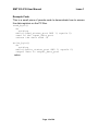
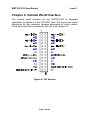
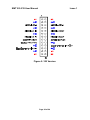
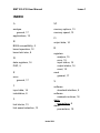
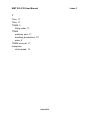
SMT103-ICG
User Manual
Version 1.0
Provisional Draft
Document:
Product Name:
Author:
SMT103-ICG User Guide.doc
User Manual
Mark Ainsworth
Issue : 01
Revision Date:
Original Date:
Rev.: 1.11
9 September 1998
3 April 1997
Disclaimer
Every effort has been made to ensure the accuracy of this
document, however the manufacturer cannot accept
responsibility for any loss or damage caused as a result of
using this document.
Notice of any mistakes, inconsistencies or comments
relating to this document would be gratefully received by
fax or email to Sundance.
Fax No. +44 (0)1494 726363
email [email protected]
Technical Support
Technical support is available by the following methods:
Telephone
Fax
email
+44 (0)1494 431203
+44 (0) 1494 726363
[email protected]
For UK users a local call line is available:
Telephone
01345 626791
Sundance now operate a World Wide Web page, and information is
posted on a regular basis to provide our customers with the most up
to date information concerning our products.
http://www.sundance.com/
Page 1 of 24
SMT103 USER MANUAL
ISSUE 1
Table of Contents
Table of Contents ......................................................................... 2
Table of Figures............................................................................ 3
Table of Tables ............................................................................. 4
Chapter 1 General Introduction ................................................... 5
The Manual ............................................................................. 6
Chapter 2 Installation ................................................................... 8
Prepare the Host PC and insert the board ............................... 8
Chapter 3. Fitting the TRAMs..................................................... 10
Handling Precautions ............................................................ 10
Which slot(s) to use............................................................... 10
How to fit a TRAM ................................................................. 11
Chapter 4 Using the SMT103-ICG .............................................. 12
Chapter 5 Switches..................................................................... 13
Version Selection .................................................................. 13
Transputer and TRAM Link Speed Selection ......................... 13
Transputer Clock Speed Selection......................................... 13
Transputer Memory Speed Selection..................................... 13
The Internal Reset, Analyse and Error lines........................... 13
Chapter 6. Programmable Registers.......................................... 14
Input data registers, Output data registers...................... 14
Input Status registers, Output Status registers................ 14
Error Register ................................................................ 15
Reset Register ............................................................... 15
Analyse Register............................................................ 15
Example Code ...................................................................... 16
Chapter 7. What are Reset, Analyse and Error?........................ 17
Chapter 8. Outside World Interface ........................................... 19
Bibliography ............................................................................. XXI
INDEX ....................................................................................... XXII
Page 2 of 24
SMT103 USER MANUAL
ISSUE 1
Table of Figures
TRAM slot positions................................................................... 10
Transnputer speed selection ..................................................... 13
Page 3 of 24
SMT103 USER MANUAL
ISSUE 1
Table of Tables
Jumper colour allocation ........................................................... 13
PC Port IO Map ........................................................................... 14
Input [output] Status Register ................................................... 15
Error Register ............................................................................. 15
Reset Register............................................................................. 15
Page 4 of 24
SMT103-ICG User Manual
Issue 1
Chapter 1 General Introduction
The INMOS pioneered, Parallel Processing standard is built around
that of the TRAM (TRAnsputer Module) concept, which consists of a
variety of module sizes. These vary from the smallest size 1
(3.66''x1.05'") to the largest size 8 (3.66'' x 8.40''). TRAMs may
contain a transputer, some memory and other various I/O functions.
These may include Analog to Digital converters; IEEE interfaces;
SCSI controllers, and high resolution graphics devices.
The TRAM format has also been used by many manufacturers to
integrate sequential processors like Intel's i860 Vector processor,
Motorola's 56000/96000 DSP, Zoran's Vector DSPs and AT&T's
DSPs into transputer networks. The only other truly parallel
processing processor, Texas Instruments TMS32C40 pDSP, has
also been incorporated into a TRAM format using a size 4 board.
The front-end computer host system for transputers and TRAMs
span from minimum PC/XTs to high-end SUN and VAX
workstations. They all have a basic common interface protocol, the
INMOS AFServer, with different hardware implementations. This
protocol was introduced by INMOS with their first product for the PC,
the INMOS B004 PC plug-in board. The INMOS B004 standard was
extended with the arrival of the TRAM concept and the INMOS B008
10-slot TRAM motherboard for the PC.
The SMT103-ICG is a cost-effective TRAM motherboard, and
integrated transputer system. It can take up to four size 1 TRAMs, in
addition to the onboard transputer and memory system. This
onboard system can support up to 16 MBytes of dynamic memory
with a 25MHz transputer. Compatibility with the INMOS B004
industry standard provide the user with maximum flexibility.
Highly integrated component usage on the PC interface, and
extensive use of surface mount technology has enabled the
SMT103-ICG to be condensed onto a board no bigger than a
standard 8-bit interface card. This form factor will allow the SMT103ICG to be used in most old PC/XTs desktop computers and current
generation laptop and notebook computers. It is also possible to use
Page 5 of 24
SMT103-ICG User Manual
Issue 1
other processor types from other manufactures if their interface
matches that of TRAMs.
The SMT103-ICG is manufactured by Sundance Multiprocessor
Technology Limited, a high quality manufacturer of parallel
processing products. It is covered by a one Year, return to factory,
warranty from the date of purchase.
The Manual
All the sections in this manual should be read before any attempt is
made to install the board. It outlines the differences between the two
different configurations for this board.
Figures 1and 2 show the configurations of the TRAMs and the host
transputer for the two versions of the board. Both of these
configurations are achieved using the same product, simply
changing a PCB link achieves the changes required.
1
Slot 1
2
0
2
3
1
Host
2
0
Slot 0
3
3
1
Slot 2
2
0
0
3
1
Slot 3
0
notReset, notAnalyse
and notError signals
PC
Figure 1: 355 Version
Page 6 of 24
SMT103-ICG User Manual
3
1
Host
2
Issue 1
2
3
0
Slot 0
0
notReset, notAnalyse
and notError signals
PC
Figure 2: 330 Version
Page 7 of 24
SMT103-ICG User Manual
Issue 1
Chapter 2 Installation
Unpack the SMT103-ICG from its container and inspect it visually. If
there is any sign of damage to the board or components then go no
further, but inform the carrier and Sundance.
Turn off and disconnect the power from your IBM PC-XT, AT, or
clone. Consult the manual supplied with your PC for instructions on
how to insert add-in circuit boards. Insert the SMT103-ICG into any
convenient 8-bit card slot. Replace the PC cover or casing and
reconnect the power and turn on.
Observe normal anti-static handling precautions when working
with all electronic circuits. If one is available, use a wrist-strap
grounding system. If not, then always touch a properly grounded
bare metal surface BEFORE handling any circuit. Also avoid all
contact with connector pins on plug in cards and components.
TRAMs can easily sustain mechanical damage, the connector pins
are easily bent by misalignment with their sockets on insertion, or by
dropping them. The pins are expensive to replace, and on some
boards they are impossible to remove. Many TRAMs that can be
purchased use surface mount technology. These types of
components are fragile. They can easily be ripped off the surface of
the PCB by very rough handling.
Prepare the board by inserting your choice of transputer modules,
connecting the links and checking the jumper settings.
Prepare the Host PC and insert the board
1. Turn off the power to your PC and remove the system unit cover
following the instructions supplied with your system. If in doubt,
consult your dealer.
2. Select a slot in your PC. Remember that you only need to use
an 8-bit slot. When you are deciding which slot to use please
note that some TRAMs have a very high profile. You may not be
able to place your board in a slot next to another slot that
already has a board in it. Take care to ensure that the TRAMs
do not foul on the underside of any existing boards.
Page 8 of 24
SMT103-ICG User Manual
Issue 1
3. Remove the metal blanking plate from the aperture in the
system box that will hold the SMT103-ICG connector.
4. Insert the SMT103-ICG into the PC, holding it true both
vertically and horizontally to avoid catching any adjacent cards.
5. Push the SMT103-ICG firmly into the PC connector. Apply
careful but firm pressure to the top centre of the card. Do not
press on the modules or components.
6. Replace the PC cover and reconnect the system to the power.
Page 9 of 24
SMT103-ICG User Manual
Issue 1
Chapter 3. Fitting the TRAMs
Handling Precautions
Observe normal anti-static handling precautions when working
with all electronic circuits. If one is available, use a wrist-strap
grounding system. If not, then always touch a properly grounded
bare metal surface BEFORE handling any circuit. Also avoid all
contact with connector pins on plug in cards and components.
TRAMs can easily sustain mechanical damage, The gold connector
pins are easily bent by misalignment with their sockets on insertion,
or by dropping them. The pins are expensive to replace, and on
some boards they are impossible to remove. Many TRAMs that can
be purchased use surface mount technology. These types of
components are fragile. They can easily be ripped off the surface of
the PCB by very rough handling.
Slot 0
Slot 2
Slot 1
Slot 3
Figure 3. TRAM slot positions
Which slot(s) to use
Please refer to figure 3 for a map of the positions, orientation and
numbering of the TRAM slots. For a 355 version board then TRAMs
Page 10 of 24
SMT103-ICG User Manual
Issue 1
are fitted in all 4 slots. For a version 330 then only one TRAM is
fitted, and this is put into slot 0.
How to fit a TRAM
1. TRAMs should have a white or yellow triangle marked on the
printed circuit board in the corner by pin 1. Match this up with
the pin 1 triangle on the SMT103-ICG. If there is no triangle
marked on the TRAM then please consult the manufacturer's
manual or the board supplier. The effort may well save you
damaging the TRAM.
2. Most TRAMs are supplied with extension pins fitted to the strip
sockets to protect them in transit. Remove them with a small
pair of pliers or tweezers and store them safely. You will need to
use them if the TRAM ever has to be returned for repair. Take
great care not to bend the pins soldered to the TRAM. If you are
stacking one TRAM on top of another then keep the extenders in
place.
3. Line up all the TRAM pins visually before inserting them in the
motherboard sockets. When you are quite sure that the pins are
aligned and partially inserted, the TRAM will push home with
gentle but firm pressure.
Removal is the reverse of fitting. The TRAMs will have to be gently
levered out using a small screwdriver. Be careful not to bend the
TRAM pins.
Page 11 of 24
SMT103-ICG User Manual
Issue 1
Chapter 4 Using the SMT103-ICG
The SMT103-ICG is designed specifically for ICG Ltd, as so any use
options are specific to this company.
Any queries regarding the configuration and operation of this board
within an ICG should be dealt with by ICG Ltd. Directly.
Page 12 of 24
SMT103-ICG User Manual
Issue 1
Chapter 5 Switches
The SMT103-ICG has only a single link which is used to change the
operation of the board. This changes the internal link configuration
from that of a 355 to a 330 machine.
Version Selection
To switch between the two versions of the board you have to change
the settings of J4. Connecting pins 1 to 2 will select a 355 variant.
Connecting pins 2 to 3 will select a 330 variant. Do not change this
link while the board is in a system with the power applied.
The pin allocations on the connector for the ADC board will change
so make sure you have the right cable fitted to the board if you
change this setting.
Transputer and TRAM Link Speed Selection
The transputer fitted on the SMT103-ICG has four links that may be
connected to other Inmos Link interfaces. The transmission speed of
these four links, as well as the bus interface C011 and the TRAMs is
fixed at 20 Mbits/sec
Transputer Clock Speed Selection
The transputer clock speed is fixed at 25MHz.
Transputer Memory Speed Selection
The memory speed is set at 3 cycles. This is the maximum speed
allowable for DRAM.
The Internal Reset, Analyse and Error lines
The Reset, Analyse and Error lines connected to the onboard
transputer and the TRAM sites are controlled from the PC bus
interface. There is no option to change this configuration.
Page 13 of 24
SMT103-ICG User Manual
Issue 1
Chapter 6. Programmable Registers
On the SMT103-ICG there is a set of software controllable registers.
These registers are only accessible from the PC host and are used
to control the operation of the board and are mapped as IO ports.
They perform various control functions required for link
communication, as well as allowing the user to control the status of
external transputer networks
Address
#300
#301
#302
#303
#310
#310
#311
Register
Input Data Register ( ro )
Output Data Register ( wo )
Input Status Register ( rw )
Output Status Register ( rw)
Error Register ( ro )
Reset Register ( wo )
Analyse Register( wo )
Table 1. PC Port IO Map
Input data registers, Output data registers
These two registers are located inside the C011 chip. The functions
of the input data register and output data register are fairly obvious.
When the status registers indicate that they are either ready to
receive valid data, or they contain valid data then the data is written
to or read from these registers.
Input Status registers, Output Status registers
These registers are contained in the C011 chips, one set per device
and indicate the status of the input and output data registers. See
table 2 for further information.
Page 14 of 24
SMT103-ICG User Manual
rd
Bit 0
Issue 1
"0" no input data [output not ready]
"1" valid input data [output ready]
wr
Bit 1
"0" disable input [output] interrupt
"1" enable input [output] interrupt
Table 2. Input [output] Status Register
Error Register
This is a software readable port that indicates the Error status of the
transputer network connected to the PCNotError line. This is a wire
or of the main onboard transputer and any fitted TRAMS
rd
Bit 0
"0" Error false
"1" Error true
Table 3. Error Register
Reset Register
This register can be written to control the state of the PCNotReset
line. This can then be used to control an external transputer network,
as well as the onboard transputer and any fitted TRAMs.
wr
Bit 0
"0" Reset [Analyse] false
"1" Reset [Analyse] true
Table 4. Reset and Analyse Register
Analyse Register
This register can be written to control the state of the PCNotAnalyse
line of the onboard transputer and any fitted TRAMs and external
transputer network.
Page 15 of 24
SMT103-ICG User Manual
Issue 1
Example Code
This is a small piece of pseudo-code to demonstrate how to access
the data registers on the PC Bus.
read_byte()
do
nothing
while((read_status_port AND 1) equals 0)
read in the input_data_port
return the data read in
write_byte()
do
nothing
while((write_status_port AND 1) equals 0)
output data to output_data_port
return
Page 16 of 24
SMT103-ICG User Manual
Issue 1
Chapter 7. What are Reset, Analyse and
Error?
These three signals are used to control the operation of the
transputer. Their names pretty well describe their functions in the
system. The Reset line does exactly what it suggests. It is used to
Reset transputers. When the signal is true, whatever transputers are
connected to the
signal are put into the reset state. They
immediately stop processing and go into an idle state. When this
signal is taken not true, how the transputer behaves will depend on
the state of the Analyse line. If this line is also Not True then the
transputer will initiate the boot process and then go into either the
idle state and wait for a message on one of its links, or boot code
from EPROM space. If the Analyse signal is true when the Reset
line is taken Not True then the transputer will not perform any of the
memory configuration read cycles, or any initial DRAM refresh
cycles, but will enter a halted state. It will then remain in the halted
state until it is told to do otherwise. For more detailed information
read the Inmos T425/T805 etc. technical data sheets.
The Analyse line can be used to debug transputers whilst they are
operating. If the Analyse line is taken True without the Reset line
being taken True as well then the transputer will try to enter a halt
state. It will enter the halt state at the next descheduling point. From
Analyse being taken True the transputer will halt within 3 time slice
periods plus the time taken for any high priority process to complete.
As much of the transputer state is saved to allow remote transputers
to debug the internal state of the transputer when it was halted. After
Analysing a transputer it must be Reset otherwise its state is
undefined. For more detailed information read the Inmos
T425/T805 etc. technical data sheets.
The Error line indicates the error status of any transputer. This
output from the transputer can be set either directly from software
control, or as a result from performing instructions that generate
error conditions. For a complete list of instructions, and how they
Page 17 of 24
SMT103-ICG User Manual
Issue 1
may cause error conditions refer to the Inmos T425/T805 etc.
technical data sheets.
Page 18 of 24
SMT103-ICG User Manual
Issue 1
Chapter 8. Outside World Interface
The outside world interface for the SMT103-ICG is designed
specifically to interface to the ICG ADC card. The layout and signal
allocations for this connector changes depending on which version
of the board has been selected by the use of link jumper J4
Figure 4: 355 Version
Page 19 of 24
SMT103-ICG User Manual
Issue 1
Figure 5: 330 Version
Page 20 of 24
SMT103-ICG User Manual
Issue 1
Bibliography
[1]
Trevor Watson and Michel Rygol, INMOS
Technical Note 18; Connecting INMOS Links.
INMOS, 1987
[2]
Stephen Ghee, INMOS Technical Note 11; IMS
B004 IBM PC add-in board, INMOS, 1987
Bibliography XXI
SMT103-ICG User Manual
Issue 1
INDEX
A
M
analyse
general, 17
applications, 12
memory options, 13
memory speed, 13
O
B
B004 compatibility, 5
board operation, 12
board slot size, 8
D
data registers, 14
DSP, 5
E
error
general, 17
I
input data, 14
installation, 8
L
link blocks, 13
link speed selection, 13
output data, 14
R
registers
analyse, 15
error, 15
input status, 14
output status, 14
reset, 15
reset
general, 17
S
software
standard interface, 5
software
example routines, 16
static
precautions, 8
static
precautions, 10
Index XXII
SMT103-ICG User Manual
Issue 1
T
T4xx, 17
T8xx, 17
TRAM, 5
fitting order, 11
TRAM
extender pins, 11
handling precautions, 10
sizes, 5
TRAM removal, 11
transputer
clock speed, 13
Index XXIII