1
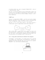
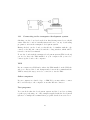
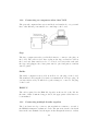
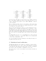
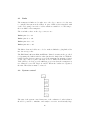
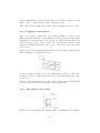
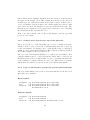
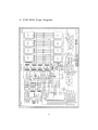
IMS B001
evaluation board
User Manual
INMOS Limited
September 1985
72-BRD-009-01
You may not:
1. Modify the Materials or use them for any commercial purpose, or any public
display, performance, sale or rental;
2. Remove any copyright or other proprietary notices from the Materials;
This document is distributed in the hope that it will be useful, but WITHOUT
ANY WARRANTY; without even the implied warranty of MERCHANTABILITY
or FITNESS FOR A PARTICULAR PURPOSE.
INMOS, IMS, OCCAM are trademarks of INMOS Limited.
INMOS Limited is a member of the SGS-THOMSON Microelectronics Group.
2
Contents
Preface
5
1 Getting started with IMS B001
1.1 Opening the bag . . . . . . . . . . . . . . . . . . .
1.2 Mounting the board for use . . . . . . . . . . . . .
1.3 Power supply . . . . . . . . . . . . . . . . . . . . .
1.4 Connecting up to the power supply . . . . . . . . .
1.5 Checking the setting of the coding switches . . . .
1.6 Resetting the board . . . . . . . . . . . . . . . . .
1.7 Connecting to a terminal . . . . . . . . . . . . . .
1.8 Autobaud . . . . . . . . . . . . . . . . . . . . . . .
1.9 Testing the board . . . . . . . . . . . . . . . . . . .
1.10 Using the board between terminal and computer .
1.11 Connecting to the transputer development system
1.12 Connecting to computers other than VAX . . . . .
1.13 Connecting multiple boards together . . . . . . . .
.
.
.
.
.
.
.
.
.
.
.
.
.
.
.
.
.
.
.
.
.
.
.
.
.
.
.
.
.
.
.
.
.
.
.
.
.
.
.
.
.
.
.
.
.
.
.
.
.
.
.
.
.
.
.
.
.
.
.
.
.
.
.
.
.
.
.
.
.
.
.
.
.
.
.
.
.
.
6
6
6
7
8
8
9
10
10
11
12
13
14
14
2 Evaluation board architecture
15
2.1 Links . . . . . . . . . . . . . . . . . . . . . . . . . . . . . . . . 16
2.2 System control . . . . . . . . . . . . . . . . . . . . . . . . . . 16
2.2.1 Plugging boards together . . . . . . . . . . . . . . . . 17
2.2.2 The signals on the sockets . . . . . . . . . . . . . . . . 17
2.2.3 Control of the board at the top of the hierarchy . . . . 18
2.2.4 Logic on the board to provide the system control functions . . . . . . . . . . . . . . . . . . . . . . . . . . . . 18
2.3 Edge connector pinout . . . . . . . . . . . . . . . . . . . . . . 19
3 IMS B001 T414 evaluation board Software
3.1 Using the board . . . . . . . . . . . . . . . .
3.2 EPROM monitor . . . . . . . . . . . . . . .
3.2.1 Transparent . . . . . . . . . . . . . .
3.2.2 Active . . . . . . . . . . . . . . . . .
3.3 Self test . . . . . . . . . . . . . . . . . . . .
3.4 Example programs . . . . . . . . . . . . . .
3.4.1 Terminal driver . . . . . . . . . . . .
3.4.2 Multi-board echo test . . . . . . . .
.
.
.
.
.
.
.
.
.
.
.
.
.
.
.
.
.
.
.
.
.
.
.
.
.
.
.
.
.
.
.
.
.
.
.
.
.
.
.
.
.
.
.
.
.
.
.
.
.
.
.
.
.
.
.
.
.
.
.
.
.
.
.
.
.
.
.
.
.
.
.
.
.
.
.
.
.
.
.
.
21
21
21
22
23
24
26
26
27
4 Memory map and peripherals
27
4.1 Memory map . . . . . . . . . . . . . . . . . . . . . . . . . . . 27
4.2 Peripherals . . . . . . . . . . . . . . . . . . . . . . . . . . . . 28
5 IMS B001 Evaluation board accessories
3
30
6 IMS B001 D cables
30
7 IMS B001 Component layout
31
8 IMS B001 Logic diagram
32
4
Preface
The IMS B001 evaluation board enables users to evaluate and demonstrate
the use of transputers. The board is the first of a family of compatible
evaluation boards. It provides standard buffered INMOS link connections
and external control of the transputer’s Reset and Analyse functions. This
allows it to control a subsystem consisting of other compatible boards, or to
be a component of such a subsystem.
This manual details the product specific aspects of the IMS B001, and contains all the data necessary to power up, test and program the board.
Other information relevant to all transputer products is contained in the
occam programming manual (supplied with INMOS software products and
available as a separate publication), and the transputer reference manual
(supplied with this board). This board is designed to be used in conjunction
with a transputer development system, and reference should be made to the
transputer development system user manual (supplied with the development
system), for details of how to compile and load programs for a network of
boards.
Disclaimer
Every effort has been made to test this product and its operation with the transputer development system. Note, however, that the board contains a ’prequal’
version of the transputer on which engineering characterization and life tests have
not been performed.
INMOS reserves the right to make changes in specifications at any time and without
notice. The information furnished by INMOS in this publication is believed to be
accurate, but no responsibility is assumed for its use, nor for any infringements of
patents or other rights of third parties resulting from its use. No licence is granted
under any patents, trademarks or other rights of the INMOS Group of Companies.
Copyright 1985 INMOS Limited. This document may not be copied, in whole or
in part, without prior written consent of INMOS Limited.
5
1
Getting started with IMS B001
1.1
Opening the bag
When you open the bag you will find a red plastic case which contains the
board, a bunch of cables plugged into a 64 way edge connector socket, two
RS 232 cables labelled C and D, and some documentation including this
user manual.
1.2
Mounting the board for use
The red plastic case which holds the board also acts as a mounting rack for
up to six boards. The board itself is mounted on a frame, which slides into
the top of the case.
To remove the board and mount it on the top of the case:
1. Place the red case on a table so the white arrows are facing towards
you. You should also be able to see the Anti-Static warning facing you
on the frame.
2. With your thumbs, gently push apart the clips on either side of the
frame so that the frame is released.
3. Tilt the case so that the frame slides out.
4. Without touching the circuit board, withdraw the frame from the case.
6
5. When you do touch the board, touch it first at either end of the 64
way edge connector; the pins at both ends are GND.
6. Turn the frame so the Anti-Static warning faces down and the component side of the board faces you.
7. Place the frame over the white arrows on the case. Gently slide the
frame towards you into the slots either side of the case, as shown in
the white painted picture on the case.
8. When you come to plug the cables into the board, do so carefully.
Up to six frames can be mounted onto the case.
1.3
Power supply
Find a Lab power supply capable of delivering 3A at 5V, and set it to 5V,
current limiting between 2.5 and 3.0 Amps.
Voltage setup:
Current setup:
7
1.4
Connecting up to the power supply
Switch the power supply off.
Leave the bunch of cables plugged into the 64 way edge connector socket
and plug this socket onto the board.
Among the cables you will find a red banana plug and a black banana plug.
The black banana plug connects to 0V of a power supply and the red banana
plug connects to +5V of the power supply. Check you have connected the
power the right way round and switch on.
The green LED should light, indicating that the board is supplied with
power. The board should be taking about 1.6A.
WARNING:
The IMS B001 edge connector is not compatible with the edge connector of
the IMS B000. The board, possibly including the transputer, will be
damaged if a B001 is plugged into a B000 socket.
1.5
Checking the setting of the coding switches
Check the coding switches on the board. There are two sets, one of eight
switches and one of four switches. All of the four switches should be ON.
For a board containing an IMS T404, all of the eight switches should be set
8
to OFF; for a board containing an IMS T414, switch 8 should be ON and
all the others OFF.
1.6
Resetting the board
Press the push button to reset the board. The middle (red) LED should
glow brightly while the reset button is pressed, go off for a short while when
the reset button is released, and then come on a little less brightly than
while the button was pressed. In this state the board is polling the UART
to see if a terminal or host computer is connected.
9
The red LED is driven by address bit 14, which indicates something about
the activity of the program. The yellow LED should be OFF, because it
indicates Error, and the ROM program does not cause the Error flag to
become set. The green LED should stay ON to indicate that power is
supplied to the board.
1.7
Connecting to a terminal
You should be able to connect most varieties of terminal to the 25 way
socket on the board. The RS232 cables (provided with the board connect
directly to a VT100 or VT220, so you may find it easiest to use one of these
terminals. Otherwise you may need a gender changer, as shown below, to
connect to a different terminal.
Set the terminal to 8 bit characters without parity. Connect it to the socket
on the board and press the reset button. When the button is released a
message should appear on the terminal.
IMSB001 monitor. Copyright INMOS Limited 1985.
If it does not, or garbage appears on the screen, don’t worry.
1.8
Autobaud
The program in the ROM assumes the terminal is set to 9600 bit/s and
outputs the message at this speed; if the terminal is set to a different speed
the message will either not come out or will appear as garbage. The ROM
program also contains code to recognize the baud rate (see section 3.2).
10
Type A for autobaud detection. Note that typing S at this point causes the
program to enter self-test mode (see section 3.3).
The transputer recognizes the baud rate and the character and outputs the
message again at the new baud rate. It also asks if you wish to change the
load escape sequence (you don’t):
IMSB001 monitor. Copyright INMOS Limited 1985.
New load escape sequence (Y/N)?
Type N (upper or lower case) to say that you don’t want to change it, and
the terminal will say:
Transparent...
In this state, the 25 way D type plug on the board behaves just like the plug
on the back of the terminal.
1.9
Testing the board
Reset the board again. This time type S for Self Test. The transputer will
autobaud again and will prompt:
Test : M)emory, L)inks, U)art echo ?
which offers a selection of tests you can run on the board.
Memory test
Start with a memory test, by typing M (upper or lower case). The program
gives you a count of the number of successful tests, or else reports failures.
If the test fails to run or reports failures, check that the power supply, is
correctly set so that the board is receiving 5.0V and that the power supply
is not current limiting.
The memory test is described more fully in section 3.3.
Link test
Check that the link cables are properly attached to the edge connector. (The
link cables are short lengths of pairs of twisted pairs, with five way sockets
11
at each end.) As the edge connector is supplied, Link0 should be connected
to Link1 and Link2 to Link3.
Reset the board and run the link test. The most likely failure is that it locks
up and reports no successful test. If this happens, recheck that the cables
are properly connected. If the test runs successfully, it will give a count of
the successful tests.
UART test
You have been using half the UART to control the tests via the terminal.
Much the easiest way to test the other half is to use the board transparently
between a terminal and computer, as described on the next page.
Otherwise you need a gender changer which not only turns the plug into a
socket but also crosses over pins 2 and 3 of the 25 way connectors.
After you have built or acquired such a gender changer, reset the board,
type S and then U to run the U)art echo test. Unplug the terminal from
the socket on the board and plug the terminal into the gender changer. The
screen should now echo any character typed on the keyboard.
1.10
Using the board between terminal and computer
You may like to connect the plug to your computer as if you were connecting
your terminal to the computer. The board is transparent to all characters,
including break, X-On, and X-Off. The board does not, however, pass the
DTR/CTS or any other hardware handshake signals.
12
1.11
Connecting to the transputer development system
Checking out the board as described in this Getting started note should
ensure that the board is basically functional before you try downloading
programs to it from the transputer development system.
Having checked out the board you should also be familiar with the edge
connector, the RS 232 connectors and the coding switches, which will be
referred to in the User manual.
To use the board with the transputer development system (TDS for short)
you need to have the TDS installed on your computer and you need to
connect up the board to the computer.
VAX
If your computer is a VAX and you have the TDS installed on the VAX, the
way you connected the board transparently between the terminal and the
VAX is exactly the way you need to connect it to use the TDS.
Other computers
If your computer is a Stride, Sage, or IBM PC, you may wish to connect
the board directly to the computer on another RS 232 connector.
Test programs
You can check that the development system and the board are working
together properly using one of the examples supplied with the development
system, for example the terminal driver program described in section 3.4.
13
1.12
Connecting to computers other than VAX
The personal computers have screen and keyboard attached to one port and
have other RS-232 ports suitable for connecting to the board.
Sage
The Sage computer uses the port labelled Aux 1 to connect to the plug on
the board. The cable needs to have a plug at the Sage end and a socket at
the board end. Pins 2 and 3 need to be crossed over between the ends, and
the Sage end (plug) needs to have pin 4 wired to pin 5 and pins 6, 8 and 20
wired together.
Stride
The Stride computer needs a cable from Port 2 to the plug on the board.
The standard cable supplied by Stride is terminated in a D type plug. If
you have such a cable you will need a gender changer to connect to the plug
on the board.
IBM PC
The cable required for the IBM PC depends on the model of the PC. At
the time of this document being produced, the appropriate cables have not
been finalized.
1.13
Connecting multiple boards together
The board uses an edge connector pinout which is common to several of
the INMOS transputer evaluation boards. The pinout is described in detail
later in the user manual, but the figure in the margin shows most of what
14
you need to know. The pins are grouped in sets of five, suitable for the five
way sockets which terminate the various cables which plug into the edge
connector. Each five way socket is coded to make it difficult to connect it
to the wrong pins.
The power supply and link sockets are self explanatory. The banana plugs
allow several boards to use the same power supply, which should be capable
of providing the total current required.
The Up, Down, and Subsystem sockets are concerned with system control initialization and error handling. The simplest way to use them is to connect
the Subsystem socket of the board connected to the TDS to the Up socket
of the next board, and then daisy chain Down of one board to Up of the
next board, as shown below. This connection means that when you reset
the board connected to the TDS, all the other boards are reset at the same
time.
One further thing you need to do to boards which are not connected directly
to the TDS is to set them to boot from link. This is done by setting switch
7 of the 8 way coding switch to ON.
You can check that the system is running properly using the simple echo
program described in section 3.4.
2
Evaluation board architecture
The IMS B001, B002 and other evaluation boards share a common architecture which includes the edge connector pinout, link buffering, and system
control functions. The architecture is independent of the type of transputer
used, its speed, and of the number of transputers on the board.
The memory map of each board is different, and is included elsewhere in
this manual.
15
2.1
Links
The transputer’s links are brought out to the edge connector, for the user
to configure his system as he wishes. A pair of link cables is supplied with
each board, giving four ends of cables which are suitable for connecting to
the four links of the transputer.
The four link sockets on the edge connector are:
Link0 pins c7 to c11
Link1 pins a7 to a11
Link2 pins c13 to c17
Link3 pins a13 to a17
The link sockets and cables are coded to make it difficult to plug link cables
into the wrong socket.
The IMS B001 buffers its links with F244s. Printed circuitry is also provided
for bypassing the buffers with low value (such as 22 ohm) resistors. With the
buffers bypassed it is necessary to protect the transputer from static voltages
on the edge connector pins. Schottky diodes to GND in the F244s and to
VCC (discrete diodes) provide sufficient protection that the transputer is
not damaged by several ’Zaps’ at 2.0 kV. When the buffers are bypassed,
the 100 ohm resistors must be removed.
2.2
System control
The aim of the system control functions of the evaluation boards is that it
should be possible to initialize, and analyse errors in, an arbitrarily large
16
system built with the boards. In particular, one board in a cabinet or a rack
must be able to control all the other boards in the rack.
This control is necessarily independent of the serial links between boards.
2.2.1
Plugging boards together
One board controls a subsystem of an arbitrary number of other boards.
This is achieved with three sockets which we call Up, Down and Subsystem.
The figure on the left shows a board at the top with its Subsystem socket
wired to the Up socket of the board below. Subsequent boards are daisy
chained by wiring the Down socket of one board to the Up socket of the
board below.
Each of the boards in a subsystem can itself control a further subsystem, as
in the hierarchy of boards shown below.
A cable is supplied with each board which may be used to connect the
board’s Up socket to either the Down socket or the Subsystem socket of the
board above.
The Up socket is implemented as edge connector pins c28-32, and the Down
socket as pins a28-32, the subsystem socket as pins a22-26.
2.2.2
The signals on the sockets
Each of the sockets includes the signals notReset, notAnalyse and notError.
17
The notReset and notAnalyse signals flow in the direction of the arrows in
the figure in the margin, the notError signal flows in the reverse direction
from Down to Up, and indicates that an error has occurred on this board or
on a board further down from this board. All the inputs are biased so that
if a socket is not used, the signals it receives are in their inactive state. The
Subsystem error signal is not propagated up because the board controlling
the subsystem should deal with the error.
Each board has a switch each for Reset and Analyse, and an (optional)
power-on reset circuit.
2.2.3
Control of the board at the top of the hierarchy
The board at the top of the hierarchy can be reset or analysed from the
switches on the board, or from remote switches which drive the board’s Up
socket (via suitable debouncing logic). Such switches may be integrated
within a control panel which includes an Error indicator which is lit when
the notError signal on the Up socket is low.
The top board of the hierarchy is likely to be connected to a terminal or host
computer which is used to control the system. These will be connected via
the RS232 ports.- It is obviously useful to be able to determine the Baud rate
of the terminal or computer attached to the ports. This is done by software
which times the pulses it receives from the ports’ RS232 data signals.
2.2.4
Logic on the board to provide the system control functions
The logic relationships between the sockets and switches are shown below
(ignoring logic polarities).
Reset signals
Transputer = Up OR
Down
= Up OR
Subsystem = Up OR
OR
DebouncedSwitch OR LocalPowerOn
DebouncedSwitch OR LocalPowerOn
DebouncedSwitch OR LocalPowerOn
Addressable Latch
Analyse signals
Transputer = Up OR DebouncedSwitch
Down
= Up OR DebouncedSwitch
Subsystem = Up OR DebouncedSwitch OR Addressable Latch
18
Error signals
Up
= Transputer OR Down
LED
= Up
Addressable input = Subsystem
Subsystem latches
The addressable latches for subsystem reset and subsystem analyse are initialized at power-on to be inactive, ie not resetting and not analysing the
subsystem.
2.3
Edge connector pinout
The boards use a two part edge connector conforming to DIN 41612, the
same sort of connector as is used on VME boards and Multibus II boards.
IMS B001 and B002 boards use the 64 way version of this connector, with
the pinout shown.
The GND pins c31,32 on the board are convenient for scope earth leads.
19
Pin
1
2
3
4
5
c
GND
VCC
(cut short)
VCC
GND
b
a
GND
VCC
(cut short)
VCC
GND
6
7
8
9
10
11
(sleeved)
GND
(cut short)
LinkOut[0]
LinkIn[0]
GND
(sleeved)
GND
(cut short)
LinkOut[1]
LinkIn[1]
GND
12
13
14
15
16
17
(sleeved)
GND
(cut short)
LinkOut[2]
LinkIn[2]
GND
(sleeved)
GND
(cut short)
LinkOut[3]
LinkIn[3]
GND
18
19
20
21
22
23
24
25
26
(sleeved)
PIO0*
PIO1*
PIO2*
PIO3*
PIO4*
PIO5*
PIO6*
PIO7*
(sleeved)
NC
notBootFromROM*
(sleeved)
SubsystemNotReset
SubsystemNotAnalyse
SubsystemNotError
GND(cut short)
(cut short)
27
28
29
30
31
32
(sleeved)
UpNotReset
UpNotAnalyse
UpNotError
GND
GND(cut short)
(sleeved)
DownNotReset
DownNotAnalyse
DownNotError
GND(cut short)
GND(cut short)
* The B001 board does not implement the PIO pins, nor the notBootFromROM pin.
20
3
IMS B001 T414 evaluation board Software
The IMS B001 transputer evaluation board contains a monitor in EPROM
which allows the user some flexibility in the use of the board. This document describes the software in the EPROMS. The terminal driver software
supplied with the transputer development utilities is also described.
3.1
Using the board
The monitor on the board has been designed so that the board can be used
as a peripheral to a workstation such as a Stride or transparently between
a terminal and a host system such as when used with a VAX. A description
of how to connect the board to a host computer system can be found in the
Getting started section of this manual.
3.2
EPROM monitor
On power-up or reset both RS232 lines are initialised to 9600 baud and the
message
IMS B001 monitor. Copyright INMOS Limited 1985.
is output to the terminal. The monitor then polls both serial lines waiting
for an incoming character. If the first character is received from the host,
the monitor enters an active mode ready to load a transputer program.
If the first character is received from the terminal, the monitor enters an
interactive mode to set up various options. If the first character typed is the
letter a (or A), the options to be set up are prior to becoming transparent.
If the first character typed is the letter s (or S), the options available are
for selecting from a set of self-test functions.
The first character received, whether from host or terminal, is used by the
monitor to determine the baud rate of that line. If the first character is received is from the host, the baud rate of the host line is set to the determined
baud rate. If the first character received is an a from the terminal then the
baud rates of both the terminal and the host lines are set to the determined
baud rate. If the first character received is an s from the terminal, then
the baud rate of the terminal line is set to the determined baud rate. The
baud rate is calculated by timing the length of the start bit of the incoming
character, consequently only characters which change state after the start
bit, will enable correct baud rate detection. The valid characters are those
with odd ASCII values, e.g. A, C, E, ... All such characters other than s
21
and S will be treated as a. Note that Space is not a valid character for the
autobaud program.
If the first character received is from the terminal and the baud rate is not
9600, the above message will be repeated at the new baud rate. If an invalid
character for baud rate detection was typed, the message may appear as a
sequence of spurious characters. In this case, reset the board and type one
of the correct characters given above.
3.2.1
Transparent
If the first character received is from the terminal, and the character is
not s or S. the monitor prepares for the board to be used transparently.
When the board is transparent, all characters received from the host are
retransmitted to the terminal and all characters received from the terminal
are retransmitted to the host. Break is transmitted from the terminal to
the host in a manner which duplicates the action of the terminal. Break is
not transmitted from the host to the terminal.
Transparent mode is terminated on receipt of a defined character sequence
from the terminal. The monitor then enters active mode. The character
sequence which terminates the transparent mode is redefinable after board
reset. Prior to becoming transparent the monitor displays the following
message
New load escape sequence (N/Y)?
This interaction allows the user to change the load escape character sequence which will terminate transparent mode and enter active mode. The
default load escape sequence is ESC ESC ESC (three characters with the
hexadecimal values 1B). The response Y will cause the message
Type new sequence, followed by return
to appear. The required escape sequence should then be typed up to a
maximum of eight characters. The new sequence is terminated by typing
carriage return or if eight characters have been typed. The carriage return
is not included as part of the sequence. The typed characters are not echoed
to the screen.
After entering the new escape sequence (or not) the message
Transparent...
22
appears. The board will remain in transparent mode until the specified
load escape sequence is typed on the terminal. The load escape sequence
should only be typed in response to the prompt received after activating the
network loading utility on the host. The prompt character is
?
When the load escape sequence has been typed the board enters active mode.
3.2.2
Active
If the first character received was from the host, or if the load escape sequence has been typed to terminate transparent mode, the monitor enters
active mode ready for the startup handshake sequence prior to loading. The
message
Active...
is displayed. The next two messages received from the host determine the
communication mode, whether BINARY or HEX, and the function. The
only valid function is load. If a correct startup handshake sequence has
occurred the message
Loading...
is displayed. The board monitor is now ready to receive loading and distribution data packets. Each code packet successfully received by the monitor
will cause the character . (period) to be sent to the terminal line. The only
way to return to transparent operation after active mode has been entered
is by reseting the board.
Error messages
If the monitor detects an error during loading one of the following messages
will be displayed on the terminal. In all cases the error LED on the board
will be switched on and the monitor will STOP. The loading errors all have
the format
ERROR during load : error.message
All messages with exactly this format will have been generated by the monitor software on the board. The messages are:
23
Invalid board function The board function received was not load.
Invalid character received This message occurs only when the board is
being loaded using encoded hex. The message indicates that a character received was not a character from the set used in this communication mode.
Invalid checksum The checksum character received did not match that
calculated.
Invalid command A message protocol failure has occurred. This message
should not normally appear.
Invalid communication mode The communication mode character received was neither B nor H. This condition arises when the baud
rates are not consistent at both ends of the board to host line, when
a board has not been reset prior to loading or when a board has been
reset after receipt of the wakeup character.
3.3
Self test
If the initial character received by the EPROM monitor was an s or S from
the terminal, the monitor displays the following message
Test: M)emory, L)inks, U)art echo
RAM test
If the character m or M is typed the following message appears
Testing RAM...
The monitor the cycles through the on board RAM reading and writing in
various different combinations. After each complete cycle the message
Tests so far = number. Failures so far = number
will be printed so that it overwrites the current cursor position. If a failure
occurs, the message
Failure at address : number C)ontinue, S)uppress
messages and continue or R)etry ?
24
will appear. If the character c or C is typed, the RAM test continues
at the next address. This will normally generate another failure message
immediately. If the character s or S is typed the RAM test continues but
only prints out the message produced at the end of the complete cycle.
Normally the Failures so far count will increase rapidly because the value
is incremented for each test that fails. If the character r or R is typed
the monitor continues with the current action on the failing address. If
C)ontinue is typed the failure messages will move down the screen partially
overwriting the C)ontinue prompt.
To enter any other test or to restart the RAM test, the board must be reset
and s typed at the terminal.
Link test
If the character l or L is typed the following message appears
Testing links...
Links may be connected in any fashion.
Errors on link no.
0
1
2
3
Test
Number
The link test performs an 8K-byte block transfer to all four output links
and inputs from all four input links in parallel. The received data is then
checked for validity. The link test requires that all the links are connected,
though it does not matter in which order. If a link is not working at all, the
test will fail and not print any information at all. If a link is transferring
incorrect information the error count for that link will be incremented.
Uart echo test
If the character u or U is typed the following message appears
Host uart echo test...
This test is a simple program which echos all characters received on the host
line. It is assumed that the terminal line is working in order to get this far in
the test sequence. The terminal should be disconnected from the terminal
connection on the board and reconnected on the host connection (this will
require a gender changer with pins 2 and 3 crossed over). All characters
typed should then be echoed to the screen.
25
3.4
Example programs
Some example programs are provided with the transputer development utilities software. The purpose of these is to help familiarise the user with the
use of the boards and to act as a check that the boards are working. The
terminal driver program is described below, the other examples supplied will
include instructions on how to use them.
3.4.1
Terminal driver
To speed porting programs to run on the board, a separately compiled process called terminal.driver is supplied. This handles I/O via the RS232
interfaces and provides a pair of channels through which the users program
can access a terminal. Most occam programs will have been written using channels to access the computer’s keyboard and screen and, in these
cases it will only be necessary to run terminal.driver in parallel with the
users process to execute the program on the transputer. For example, to
communicate with a 9600 baud device connected to the terminal port:
CHAN keyboard, screen :
DEF terminal =
0 :
DEF baud.rate = 9600 :
PAR
terminal.driver (keyboard, screen, terminal, baud.rate)
user.process
(keyboard, screen)
Terminal driver parameters
The process has two channel parameters for input and output (screen and
keyboard above) and two value parameters. These determine which RS232
port is to be used and the baud rate.
The first parameter selects the terminal or host port:
DEF terminal = 0 :
DEF host
= 1 :
The second parameter selects the desired baud rate. Valid settings are:
38400 19200
4800 2400
9600
2000
7200
1800
26
1200
200
75
1050
150
50
600
134
300
110
If an invalid setting is selected the terminal driver defaults to 38400.
Note that the terminal driver provides all eight bits of character information
it receives. If the terminal has been set to generate even parity characters,
then it will be necessary to remove the parity bit by software before comparing character values.
3.4.2
Multi-board echo test
A simple program is provided with the TDS which can be run on one board
or as many boards as you have. All the program does is to echo characters
typed on the keyboard, but the characters are sent down all the boards in
the system, and then back again. You will need to change the DEF for the
number of boards (the constant identified as processors in the program),
and wire the links up as instructed by the Wiring Diagram produced by the
TDS when you configure the program for multiple boards.
4
4.1
Memory map and peripherals
Memory map
The memory on the board includes 64 kbytes of RAM, 128 kbytes of ROM,
and peripherals. Transputer addresses are signed integers, so the address
map is as follows:
27
7FFFFFFF
........
7FFE0000
EPROM
80058000
80050000
80048000
80040000
Unused peripheral
Readable switches and RS232 data
Subsystem latches in PAL
DUART registers
8000FFFF
........
80000800
Top of RAM
800007FF
........
80000000
Top of on-chip RAM for T414
EPROM
Bottom of external RAM with T414
Bottom of on-chip RAM
The addresses are not fully decoded, so the memory map is repeated throughout the address space.
4.2
Peripherals
There are three peripherals, the DUART, the readable switches and RS232
data, and the Subsystem latches in the PAL.
DUART
The DUART, for the two RS232 ports, is mapped into the bottom of the
peripheral area and has 16 registers within it. These are decoded to be on
word boundaries. The A side of the DUART is connected to the D type
socket, which is normally used to connect to a terminal; the B side of the
DUART is connected to the D type plug, which is normally used to connect
to a host computer. For further details consult the 2681 data sheet.
D type socket (for terminal)
The D type socket has serial data transmitted on pin 3 and received on
pin 2. This means that for most terminals a straight cable is required, with
pin 2 connected to pin 2 and pin 3 connected to pin 3.
28
D type plug (for host computer)
The D type plug has serial data transmitted on pin 2 and received on pin 3.
This means that for most terminals a straight cable is required, with pin 2
connected to pin 2 and pin 3 connected to pin 3.
Both RS232 cables provided (cables C and D) have straight connections,
between a plug at one end and a socket at the other end.
Subsystem latches
Subsystem Reset is written to at data bit 0 of address 80048000.
Subsystem Analyse is written to at data bit 0 of address 80048004.
Subsystem Error is read from data bit 0 of address 80048004.
Readable switches and RS232 data
The four way coding switch is readable by program, as is received data from
the RS232 ports for baud rate recognition. They are all readable at address
80050000, with bit pattern as follows:
D7
D6
D5
D4
D3
D2
D1
D0
=
=
=
=
=
=
=
=
Readable switch numbered 1 (OFF means 1, ON means
Readable switch numbered 2 (OFF means 1, ON means
Readable switch numbered 3 (OFF means 1, ON means
Readable switch numbered 4 (OFF means 1, ON means
not used
not used
Received data from D type plug (host computer)
Received data from D type socket (terminal)
29
0)
0)
0)
0)
5
IMS B001 Evaluation board accessories
Edge connector
Link cables (2 off per board)
Power supply cable
Reset cable
6
IMS B001 D cables
30
7
IMS B001 Component layout
31
8
IMS B001 Logic diagram
32