1
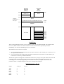
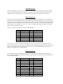
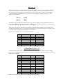
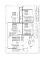
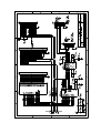
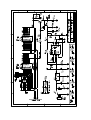
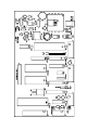
DIY Electronics
Southern Cross II
8031 Single Board Computer
Hardware Manual
DIY Electronics (HK) Ltd
PO Box 88458
Sham Shui Po
Hong Kong
Fax: (852) 2304 2250
Voice: (852) 2729 1400
Email: [email protected]
http://www.kitsrus.com
May, 2002.
Introduction
The Southern Cross II single board computer is based around the 8032/52 8-bit microcontroller. Adding a
power supply and connecting to any PC capable of running an 8051 cross-assembler enables the user to
implement an 8031 software development system. Programming in BASIC is also possible using one of the
8052-BASIC chips currently available. If your board is fitted with one of these BASIC chips then switching
from one software environment to the other is simply a matter of inserting or removing a link.
The Southern Cross II, when used in conjunction with the MVS-31 debugging monitor, implements a
complete 8031-based assembly language software development system. The extra resources provided by an
8032/52 over an 8031,(extra timer and an additional 128 bytes of internal RAM memory), together with an
independent external UART allows the user complete access to all the 8031's internal ports and timers.
Software debugging tools such as breakpoints, watchpoints and single stepping are provided by the MVS-31
monitor program. Refer to the "MVS-31 User's manual" for further details.
Getting Started
Running in 8031 mode
Insert the MVS-31 monitor EPROM into socket IC4 and ensure that jumper JP2 is set to the correct EPROM
type. An 8032/52 microcontroller chip must be used in position IC1.
1.
2.
3.
4.
5.
6.
Insert a link on jumper JP1.
Move switch SW2 to the OFF position.
Connect a 9 - 12 volt DC plug pack via power connector J7.
Connect the supplied serial cable to connector J5 ("HOST" port). Connect a terminal or PC (running
terminal emulation software) to the D25 connector on the cable. Configure the terminal or PC serial port
to 8 data bits, 1 stop bit and no parity. The baud rate should be set to 1200, 2400, 4800, 9600 or 19200
bps.
Turn on the power via switch SW3. LED D2 should light.
Press the Carriage Return ( Enter↵ ) key to trigger the MVS-31 automatic baud rate detection. A sign on
banner will appear followed by a " > " prompt. Commands may now be entered.
Running in BASIC mode
This mode requires an 8052-BASIC microcontroller chip in position IC1. A 27256 EPROM is also necessary
in position IC4 if BASIC programs are to be saved into EPROM. Ensure that jumper JP2 is set to the correct
EPROM type.
1.
2.
3.
4.
5.
6.
Remove the link from jumper JP1.
Move switch SW2 to the OFF position.
Connect a 9 - 12 volt DC plug pack via power connector J7.
Connect the supplied serial cable to connector J6 ("USER" port). Connect a terminal or PC (running
terminal emulation software) to the D25 connector on the cable. Configure the terminal or PC serial port
to 8 data bits, 1 stop bit and no parity. The baud rate should be set to 1200, 2400, 4800, 9600 or 19200
bps.
Turn on the power via switch SW3. LED D2 should light.
Press the space bar to trigger the BASIC-52 automatic baud rate detection. A sign on message will
appear followed by a "READY" prompt. Commands may now be entered.
Please read the section on "BASIC-52 Programming" before attempting to save any programs into EPROM.
EPROM types
The Southern Cross II can use three different EPROM types, 8K (2764), 16K (27128) and 32K (27256). The
EPROM type is selected by setting jumper JP2 to the correct position as marked on the circuit board.
Note that in order to save BASIC programs in EPROM, a 27256 EPROM must be used.
Southern Cross II Memory Map
This manual does not aim to provide a detailed explanation of the architecture of the 8051 family of
microcontrollers. However a short description is necessary so that the memory decoding scheme can be
explained and understood.
The 8051 family of microcontrollers implement the Harvard memory architecture. This means that these
devices have separate address spaces for Program and Data memory, each up to 64K in size. Internal
circuitry in the microcontroller accesses the correct memory based on the instruction being executed.
As well as having separate Program and Data spaces, these microcontrollers also have internal and external
Program and Data memory. The 8051/52 series of microcontrollers can have up to 8K of internal program
memory. Thus any program address in the range 0000h to 1FFFh is directed to internal Program memory.
Any other program address is directed externally. It is possible to direct all program access externally by
disabling internal program memory. This is done by connecting the /EA pin to ground. The 8031/32 series
have no internal program memory so all program access must be directed externally. The microcontrollers
running BASIC are 8052 series chips with the BASIC interpreter stored in internal program memory.
Program memory can only be read, not written to, The /PSEN signal is used as a read strobe for any external
program memory. Data memory occupies a separate address space from Program memory. The /RD and /WR
signals are used to access external Data memory as needed. Only Data memory can be written to and
programs can only run from Program memory!
It is possible to combine all or part of the Program and Data memory into one address space. This is done by
logically ORing the /PSEN and /RD signals with the decoded memory range required and using the resultant
output as a read strobe. Combining Program and Data memory is necessary on the Southern Cross II so that
users can download and run programs.
The Southern Cross II provides 16K of RAM memory that is accessible as both Program and Data memory.
This is the area of memory where user programs are downloaded into and executed from. The other 16K of
RAM is accessible as Data memory only.
The EPROM can be an 8K, 16K or 32K type. The EPROM address space is split, with 16K located at 0000h
and the other 16K located at 8000h. The 16K block at 8000h is used to store BASIC programs when the
Southern Cross II is used as a BASIC computer! Refer to the "BASIC-52 Programming" reference manuals
for more information.
All external I/O devices such as the SPI and PPI chips are located in external data memory. Remember that
only data memory can be written to!
Figure 1 gives an overall picture of the Southern Cross II memory map.
Memory and I/O decoding is provided via two programmable logic devices (GALs). Using GALs for address
mapping adds great flexibility to the circuit design as well as significantly reducing chip count. Other memory
and I/O address mapping schemes are possible by re-programming the GALs.
Contact DIY Electronics for further information.
0000h
2000h
4000h
Common
program and ⇒
data space
External
Program
Memory
External
Data
Memory
EPROM
( MVS-31 )
EPROM
RAM
0000h
RAM
OPTIONAL CLOCK/CALENDAR( See text )
8000h
7FFFh
8000h
EPROM
C000h
SPI
PPI
I/O EXPANSION
BIT PORT 1
BIT PORT 2
BIT PORT 3
BIT PORT 4
VACANT
F000h
F400h
F800h
FC00h
FD00h
FE00h
FF00h
Fig 1
Serial Ports
These are implemented as simple "3-wire" interfaces, using just TxD, RxD and GND. The modem control
lines "CTS, DSR and DCD" are held at the RS-232 "ON" level and do not provide any hardware
handshaking. No software handshaking protocol is used either.
The Southern Cross II has two serial ports.
1.
2.
Uses the internal serial port of the 8032/52 chip and is referred to as the "USER" port. Connection is via
the 10-pin header labelled J6.
Uses an external SC2691 UART chip from Philips Components and is referred to as the "HOST" port.
Connection is via the 10-pin header labelled J5
The RS-232 signals are brought out to standard D9 connectors by using a 10-way flat ribbon cable. One end
is terminated with a 10-pin IDC plug and the other end with a crimp-style female D9 connector. By
connecting pin 1 on the 10-pin plug with pin 1 on the D9 connectors, the signals will be in the correct
positions to allow a "straight-through" connection to a D9-type PC COM port.
RS-232 Interface - J5, J6
Signal
J5, J6 pin
D9 pin
TxD
RxD
CTS
DSR
GND
DCD
3
5
6
2
9
1
2
3
8
6
5
1
Parallel I/O Ports
A number of parallel I/O ports are provided. Some are "static" in operation, meaning that any data written to
the port is latched. The other ports are "dynamic" in nature. These ports do not latch data written to them.
Output data is only valid while the port is being addressed. These ports are referred to as "bit ports".
8031 I/O ports - J1
The 8051 family of microcontrollers have four inbuilt 8-bit parallel ports, labelled P0-3. Two of these ports,
P0 and P2, are used as address/data busses when external program and data memory access is required. This
is the mode in which the Southern Cross II operates. Port bits P3.6 and P3.7 are used as /RD and /WR signals
and therefore are not available for use as I/O lines. This leaves 13 I/O lines available for use, all of port 1 and
bits 0-5 of port 3. Note that port bits P3.0 - P3.5 all have secondary functions eg. P3.0 and P3.1 are the Rx
and Tx lines for the 8031 serial port.
These 13 I/O lines are brought out to a 16-pin header labelled J1.
J1 pin
1
3
5
7
9
11
13
15
Signal
P1.0
P1.2
P1.4
P1.6
P3.0 / RxD
P3.2 / INT0
P3.4 / T0
GND
J1 pin
2
4
6
8
10
12
14
16
Signal
P1.1
P1.3
P1.5
P1.7
P3.1 / TxD
P3.3 / INT1
P3.5 / T1
GND
Port bits P1.3, P1.4 ans P1.5 also have a secondary function. They are connected via switch SW2 to the
memory decoder GAL, IC9, and used by the 8052-BASIC chips as EPROM programming control pins. These
pins are only needed by BASIC-52 when programs are to be saved into EPROM. Refer to the section on
"BASIC-52 Programming" for further details.
8255 I/O Ports - J2
Three 8-bit parallel ports are implemented using the 8255 Programmable Peripheral Interface (PPI) chip
(IC6). This chip is mapped in external data memory at address F400h. These 24 I/O lines are brought out to a
26-pin header labelled J2.
J2 pin
1
3
5
7
9
11
13
15
17
19
21
23
25
Signal
PA0
PA2
PA4
PA6
PB0
PB2
PB4
PB6
PC0
PC2
PC4
PC6
GND
J2 pin
2
4
6
8
10
12
14
16
18
20
22
24
26
Signal
PA1
PA3
PA5
PA7
PB1
PB3
PB5
PB7
PC1
PC3
PC5
PC7
GND
Bit Ports - J4
As mentioned previously, these are "dynamic" not static ports. With referrence to sheet 2 of the schematic
diagram, the 8 I/O lines are actually driven by the data bus (BAD0 - 7). The ports are formed by decoding a
256 byte memory block and using the resulting output as an active low strobe, similar to the chip enable
signals for the EPROM and RAM chips. These 4 bit ports are mapped in external data memory at the
following address locations:
Bit port 1
Bit port 2
Bit port 3
Bit port 4
FC00h
FD00h
FE00h
FF00h
Although each port is mapped into a 256 byte block, it is only one address "wide". Therefore bit port 1 can
be accessed at address FC00h, FC01h, FC02h ... etc right through to FCFFh. These ports are both input and
output ports, depending on the instruction used to access them.
These ports are pin for pin compatible to the CN1 port on the Z80 based "Southern Cross" computer, also
available from DIY Electronics. It is provided on the Southern Cross II to take advantage of a number of addon boards already available for the "Southern Cross" computer.
The bit ports are brought out to a 16-pin header labelled J4.
J4 pin
1
3
5
7
9
11
13
15
Signal
+5V
/BIT PORT 1
/BIT PORT 3
GND
BAD4
BAD5
BAD6
BAD7
J4 pin
2
4
6
8
10
12
14
16
Signal
/RESET
/BIT PORT 2
/BIT PORT 4
GND
BAD3
BAD2
BAD1
BAD0
I/O Expansion Interface - J3
A maximum of 256 bytes of I/O expansion is available via connector J3. This interface allows for further
devices to be connected to the microcontroller. The interface is mapped in external data memory beginning at
address location F800h.
J3 pin
1
3
5
7
9
11
13
15
17
19
21
23
25
Signal
A0
A2
A4
A6
AD0
AD2
AD4
AD6
/RD
RESET
/IOEXP
+5V
GND
J3 pin
2
4
6
8
10
12
14
16
18
20
22
24
26
Signal
A1
A3
A5
A7
AD1
AD3
AD5
AD7
/WR
ALE
+5V
GND
Signals preceeded by " / " are active low, all other signals are active high.
The signal " /IOEXP " is the block decode signal for the expansion interface and should be used in
conjunction with address lines A0-A7 to provide further address decoding.
Address lines A0-A7 have already been de-mulitplexed on the Southern Cross II board ie. they are actually
address lines. This allows devices with separate address and data lines to be connected to the expansion
interface directly. For those devices with a multiplexed address/data bus use signals AD0-AD7 and ALE.
Clock/Calendar
An optional clock/calendar device is available for the Southern Cross II, a Dallas Semiconductor DS1216C
Intelligent Socket. Access to this clock/calendar is provided in the MVS-31 debugging monitor.
The DS1216C contains an internal lithium battery. This keeps the clock going during power down and also
makes the CMOS RAM non-volatile ie. no loss of data when power to the Southern Cross II is removed.
Battery life is over 10 years. No circuit modifications are necessary to use the DS1216C, just plug it in
between the RAM chip and the IC socket (or solder directly to the PCB if purchased with the Southern Cross
II kit).
BASIC-52 Programming
As mentioned, the Southern Cross II board is capable of being programmed in BASIC. A number of
suppliers, such as Intel and Micromint Inc., have available an 8052 microcontroller with a BASIC interpreter
programmed into the chip's internal EPROM. The Southern Cross II needs one of these chips installed as IC1
in order run the BASIC-52 language.
BASIC-52 has the ability to store its programs into an external memory device such as EPROM.
Programming EPROMs requires a voltage level of between 12.5 and 25 volts ( depending on the EPROM ).
The Southern Cross II generates this programming voltage using a DC-DC converter chip, IC12.
The Southern Cross II is designed to use a 27256 EPROM for storing BASIC programs. These EPROMs
require a programming voltage of 12.5 volts. Before attempting to save any programs in EPROM, the
programming voltage must be set to this level. This is done by measuring the voltage on test pin TP1 and
adjusting trimpot VR1 for 12.5 volts. This procedure is only required once. However it is worth checking this
voltage periodically or whenever any problems occur with saving programs to EPROM.
The Southern Cross II only uses 27256 EPROMs for saving BASIC programs. Remove the MVS-31 monitor
EPROM and install a 27256 type in its place. The MVS-31 monitor can reside on the same 27256 EPROM
used to save BASIC programs. The monitor would reside in the bottom 8K starting at address 0000h whereas
BASIC programs are saved at address locations 8000h upwards, which is in the upper 16K of the EPROM.
The memory decoder GAL, IC9, splits the EPROM into two halves, with one half starting at 0000h and the
other half starting at 8000h. Remember to set jumper JP2 to the correct EPROM type. A number of BASIC52 programming and startup options are also available. Refer to the BASIC-52 reference manual for further
details.
BASIC-52 uses port bits P1.3, P1,4 and P1.5 as EPROM programming control lines. The function of these
lines is:
P1.3
ALE Disable
P1.4
Program pulse width
P1.5
Enable program voltage
These signals are not connected directly to the EPROM or associated programming circuitry. Instead they are
connected via switch SW2 and the memory decoder GAL, IC9. When the GAL detects a low on its pin 5, it
uses these port bits to control the output signals " /ROM_CE, SYS_ALE and /VPP_CONT ". Moving SW2 to
the " ON " position connects the port bits to the GAL and pulls pin 5 low, ready for EPROM programming.
These port bits can also be used as general purpose I/O lines and are brought out on connector J1. These pins
MUST be isolated from any external voltage levels. This would be the case if any of these pins were inputs
being "driven" from a device connected to J1. Therefore, it is advisable before saving programs to EPROM to
disconnect any device from J1.
To summarize, the following steps must be carried out before issuing a BASIC-52 programming command.
1.
2.
Disconnect any device attached to connector J1.
Move switch SW2 to the " ON " position.
Whilst the MVS-31 monitor program and BASIC programs can be stored on the same 27256 EPROM it is
advisable to use two separate EPROMs. If you wish to keep them together then make a copy of the MVS-31
EPROM and use the copy instead. The MVS-31 binary file is on the disk supplied with the Southern Cross II
computer.
References
The hardware & software for the Southern Cross 2 were developed by Frank Crivelli for DIY Electronics.
Frank can be contacted at [email protected]
The following web sites contain 80xx code & material
http://www.lvr.com
http://livewire.ee.latrobe.edu/~sjm
http://cera2.com/gatox805.htm
http://www.atmel.com