1
APPLICATION NOTE
Renesas USB MCU
USB Peripheral Mass Storage Class Driver (PMSC)
R01AN2632EJ0100
Rev.1.00
Aug 21, 2015
Introduction
This application note describes the USB peripheral mass storage class driver. This module operates in combination with
the USB basic firmware (USB-BASIC-FW). After a while calls this sample software PMSC.
The sample program of this application note is created based on "RZ/T1 group Initial Settings Rev.1.00". Please refer to
"RZ/T1 group Initial Settings application note (R01AN2554EJ0100)" about operating environment.
Target Device
RZ/T1 Group
When using this application note with other Renesas MCUs, careful evaluation is recommended after making
modifications to comply with the alternate MCU.
Related Documents
1. USB Revision 2.0 Specification
2. USB Mass Storage Class Specification Overview Revision 1.1
3. USB Mass Storage Class Bulk-Only Transport Revision 1.0, “BOT” protocol
http://www.usb.org/developers/docs/
4. RZ/T1 Group User’s Manual: Hardware (Document No.R01UH0483)
5. RZ/T1 Group Initial Settings (Document No.R01AN2554)
6. USB Peripheral Basic Firmware (Document No.R01AN2630)
Renesas Electronics Website
http://www.renesas.com/
USB Devices Page
http://www.renesas.com/prod/usb/
Content
Overview ...........................................................................................................................................2
Software Configuration .....................................................................................................................3
Peripheral Mass Storage Class Driver (PMSC) ................................................................................4
Sample Application .........................................................................................................................15
R01AN2632EJ0100 Rev.1.00
Aug 21, 2015
Page 1 of 19
Renesas USB MCU
USB Peripheral Mass Storage Class Driver (PMSC)
Overview
The PMSC comprises the BOT protocol in USB Mass Storage Class. When combined with USB-BASIC-FW, it enables
communication with a USB host as a BOT-compatible storage device.
This module supports the following functions.
・ Response to mass storage device class requests from a USB host
・ Response to storage commands which are encapsulated in the BOT protocol
Limitations
HMSC is subject to the following limitations.
The structures contain members of different types. (Depending on the compiler, this may cause address
misalignment of structure members.)
Terms and Abbreviations
APL
BOT
CBW
CSW
PCD
PMSC
USB-BASIC-FW
:
:
:
:
:
:
:
Application program
Mass storage class Bulk Only Transport.
Command Block Wrapper
Command Status Wrapper
Peripheral control driver of USB-BASIC-FW
Peripheral mass storage USB class driver
USB basic firmware for Renesas USB device
R01AN2632EJ0100 Rev.1.00
Aug 21, 2015
Page 2 of 19
Renesas USB MCU
USB Peripheral Mass Storage Class Driver (PMSC)
Software Configuration
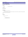
Figure 2-1 shows the configuration of PMSC, and Table 2-1 lists the modules.
User Application (APL)
Peripheral Mass Storage Class Driver (PMSC)
USB Peripheral Control Driver (PCD)
Media
USB Peripheral H/W
Figure 2-1 Software Configuration Diagram
Table 2-1 Module Function Overview
Module
APL
PMSC
PCD
Description
User application program (Please prepare for your system)
Peripheral Mass Storage Class Driver
・ respond class request
・ control BOT protocol
・ receive and analyze CBW
・ processes storage commands
・ create and send CSW
・ accesses the media
USB Peripheral H/W Control driver (USB-BASIC-FW)
R01AN2632EJ0100 Rev.1.00
Aug 21, 2015
Page 3 of 19
Renesas USB MCU
USB Peripheral Mass Storage Class Driver (PMSC)
Peripheral Mass Storage Class Driver (PMSC)
3.1
Basic Functions
The functions of PMSC are as follows:
1. Respond to mass storage class requests from USB host.
2. Respond to USB host storage commands which are encapsulated in the BOT protocol.
3.2
Class Request
Table 3-1 lists the class requests supported by the PMSC.
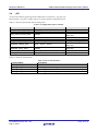
Table 3-1 Supported MSC Class Requests
Request
bRequest
Description
Mass Storage Reset
Get Max Lun
0xFF
0xFE
Resets the connection interface to the mass storage device.
Y
Reports the logical numbers supported by the device.
Y
Y:Implemented N:Not implemented(Stall response)
3.3
Supported
BOT Protocol Overview
The BOT is a transfer protocol that, encapsulates command, data, and status (results of commands) using only two
endpoints (one bulk in and one bulk out).
The storage commands and the response status are embedded in the CBW and the CSW.
Figure 3-1 shows an overview of how the BOT protocol progresses with command and status data flowing between
USB host and peripheral.
Ready
Command Block Wrapper
Command Transfer
(Host→Device)
Data-Out
(Host→Device)
Data-In
(Device→Host)
Command Status Wrapper
Status transfer
(Device→Host)
CBW transfer stage
(Command packet)
Data transfer stage
(Data packet)
CSW transfer stage
(Status packet)
Figure 3-1 BOT protocol Overview
R01AN2632EJ0100 Rev.1.00
Aug 21, 2015
Page 4 of 19
Renesas USB MCU
USB Peripheral Mass Storage Class Driver (PMSC)
3.3.1
CBW processing
When PMSC receives a CBW from the host, it first verifies the validity of the CBW. If the CBW is valid, PMSC
analysis the storage command contained in the CBW (CBWCB). PMSC finally performs processing based on the
analysis (command validity, data transfer direction and size).
When the transfer data size exceeds USB_ATAPI_BLOCK_UNIT, the data is divided into smaller units and transferred.
Data transmission commands except READ10 is created from the response data table which prepared by PMSC.
The response data table follows storage command set.
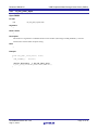
Table 3-2 lists the storage commands supported by the PMSC.
Table 3-2 Supported Storage Commands
Command
Code
TEST_UNIT_READY
0x00
REQUEST_SENSE
0x03
FORMAT_UNIT
0x04
INQUIRY
0x12
MODE_SELECT6
MODE_SENSE6
0x15
0x1A
START_STOP_UNIT
PREVENT_ALLOW
READ_FORMAT_CAPACITY
0x1B
0x1E
0x23
READ_CAPACITY
0x25
READ10
WRITE10
0x28
0x2A
SEEK
WRITE_AND_VERIFY
VERIFY10
0x2B
0x2E
0x2F
MODE_SELECT10
MODE_SENSE10
0x55
0x5A
R01AN2632EJ0100 Rev.1.00
Aug 21, 2015
Description
Type
Supported
Checks the state of the peripheral
No Data
Y
device.
Gets the state of the peripheral device.
IN
Y
Formats the logical unit.
OUT
N
Gets the parameter information of the
IN
Y
logical unit.
Specifies parameters.
OUT
N
Gets the parameters of the logical unit.
IN
N
Enables/disabled logical unit access.
No Data
N
Enables/disabled media removal.
No Data
Y
Gets the format table capacity.
IN
Y
Gets the capacity information of the
IN
Y
logical unit.
Reads data.
IN
Y
Writes data.
OUT
Y
Moves to a logical block address.
No Data
N
Writes data with verification.
OUT
N
Verifies data.
No Data
N
Specifies parameters.
OUT
Y
Gets the parameters of the logical unit.
IN
Y
Y:Implemented N:Not implemented(Stall response)
Page 5 of 19
Renesas USB MCU
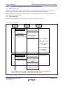
3.3.2
(a).
USB Peripheral Mass Storage Class Driver (PMSC)
Sequence of storage commands for no data transmit/receive
CBW transfer stage
PMSC issues a CBW receive request to PCD. When PCD receives the CBW, it executes a callback function which
starts the CBW transfer stage. PMSC verifies the validity of the CBW and analyzes the CBWCB.
PMSC confirms that the command is no data, compares the storage command analysis results and the information in
CBW, execute the storage command.
(b).
CSW transfer stage
PMSC creates a CSW based on the execution result and transmits it to the host via PCD.
Figure 3-2 shows the sequence.
Host
PCD
PMSC
CBW transfer state
CBW receive request
CBW receive
TEST_UNIT_READY
Transfer end interrupt
CBW receive end
callback
( CBW data )
Verify CBW validity
Verify CBW meaning
Analyze storage
command
13-case identification *
Execute storage
command
CSW transfer stage
CSW transmit resuest
CSW transmit
Transfer end interrupt
Create CSW
(CSW information)
CSW transmit end
callbak
( transfer status )
CBW receive request
* Error checking to classify 13 types of data transfer state between the host and peripherals.
Please refer to the 6.7 The Thirteen Cases of BOT specification details.
Figure 3-2 Sequence of storage commands for no data Transmit/Receive
R01AN2632EJ0100 Rev.1.00
Aug 21, 2015
Page 6 of 19
Renesas USB MCU
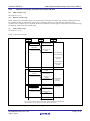
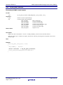
3.3.3
(a).
USB Peripheral Mass Storage Class Driver (PMSC)
Sequence of storage commands for transmit (IN) data
CBW transfer stage
The same as 3.3.2 (a).
(b).
Data IN transfer stage
PMSC notifies PCD of the data storage area and data size based on the execution result, and data communication with
the USB host. PMSC the transmission completion is notified by the PCD, to verify that the transmission of the
requested size is complete. If not completed, the DATA transmission request again to continue the DATA transfer stage.
If completed, shifts to the CSW transfer stage.
(c).
CSW transfer stage
The same as 3.3.2 (b).
Figure 3-3 shows the sequence.
Host
PCD
PMSC
CBW transfer state
CBW receive request
CBW receive
READ10
Transfer end interrupt
CBW receive end
callback
( CBW data )
Verify CBW validity
Verify CBW meaning
Analyze storage
command
13-case identification *
Execute storage
command
Data(IN) transfer stage
IN Data
Transfer end interrupt
DATA Transfer
request
( transmit Information
& transmit data)
Transfer end
callback
( transmit status )
CSW transfer stage
CSW transmit resuest
CSW transmit
Transfer end interrupt
Execute storage
command
( Final data )
Create CSW
(CSW information)
CSW transmit end
callbak
( transfer status )
CBW receive request
* Error checking to classify 13 types of data transfer state between the host and peripherals.
Please refer to the 6.7 The Thirteen Cases of BOT specification details.
Figure 3-3 Sequence of Storage Commands for Transmit (IN) Data
R01AN2632EJ0100 Rev.1.00
Aug 21, 2015
Page 7 of 19
Renesas USB MCU
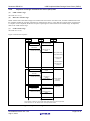
3.3.4
(a).
USB Peripheral Mass Storage Class Driver (PMSC)
Sequence of storage commands for receive (OUT) data
CBW transfer stage
The same as 3.3.2 (a).
(b).
Data OUT transfer stage
PMSC notifies PCD of the data storage area and data size based on the execution result, and data communication with
the USB host. PMSC the reception completion is notified by the PCD, to verify that the reception of the requested size
is complete. If not completed, the DATA reception request again to continue the DATA transfer stage. If completed,
shifts to the CSW transfer stage.
(c).
CSW transfer stage
The same as 3.3.2 (b).
Figure 3-4 shows the sequence.
Host
PCD
PMSC
CBW transfer state
CBW receive request
CBW receive
WRITE10
Transfer end interrupt
CBW receive end
callback
( CBW data )
Verify CBW validity
Verify CBW meaning
Analyze storage
command
13-case identification *
Execute storage
command
Data(OUT) transfer stage
DATA Transfer
request
( receive Information )
OUT data
Transfer end interrupt
Transfer end
callback
( receive status &
receive data )
CSW transfer stage
CSW transmit resuest
CSW transmit
Transfer end interrupt
Execute storage
command
( Final data )
Create CSW
(CSW information)
CSW transmit end
callbak
( transfer status )
CBW receive request
* Error checking to classify 13 types of data transfer state between the host and peripherals.
Please refer to the 6.7 The Thirteen Cases of BOT specification details.
Figure 3-4 Sequence of Storage Command for Receive (OUT) Data
R01AN2632EJ0100 Rev.1.00
Aug 21, 2015
Page 8 of 19
Renesas USB MCU
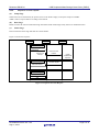
3.3.5
(a).
USB Peripheral Mass Storage Class Driver (PMSC)
Sequence of class request
Setup Stage
When PCD receives the SETUP, the process moves to the SETUP stage, to notify the reception in PMSC.
PMSC create a response data in according to the SETUP.
(b).
Data Stage
PMSC executes the control transfer data stage and notifies PCD of data stage end by means of a callback function.
(c).
Status Stage
PCD executes the status stage and ends the control transfer.
Figure 3-5 shows the sequence.
Host
PCD
PMSC
SETUP stage
Class request
GetMaxLUN
Transfer end
interrupt
Control transfer
callback
Create
GetMaxLUN
response
DATA stage
Transmit request
MaxLUN transmit
STAUS stage
OUT
ACK
Figure 3-5 Sequence for Class Request
R01AN2632EJ0100 Rev.1.00
Aug 21, 2015
Page 9 of 19
Renesas USB MCU
3.4
USB Peripheral Mass Storage Class Driver (PMSC)
API
All API calls and their supporting interface definitions are located in r_usb_pmsc_if.h.
Please modify r_usb_pmsc_config.h when User sets the module configuration option.
Table 3-3 shows the option name and the setting value.
Table 3-3 Configuration options of PMSC
Define name
USB_PMSC_USE_PIPE_IN
USB_PMSC_USE_PIPE_OUT
Default value
USB_PIPE1
USB_PIPE2
USB_ATAPI_BLOCK_UNIT
0x200ul
USB_RAM_PP
USB_SDRAM_PP
USB_MEDIA_TYPE_PP
0
1
USB_SDRAM_PP
RAMDISK_MEDIA_SIZE
(64ul * 1024ul * 1024ul)
RAMDISK_SECT_SIZE
0x200ul
RAMDISK_TOTALSECT
MEDIA_ADDRESS
(RAMDISK_MEDIASIZE / RAMDISK_SECTSIZE)
0x68000000
Description
Pipe number of IN transfer
Pipe number of OUT transfer
ATAPI block size
(byte unit)
Definition of RAM disk type
Definition of RAM disk type
Setting of Media type
Size of RAM disk type
(byte unit)
Sector size of RAM disk
(byte unit)
number of RAM disk sector
Header address of Media
Table 3-4 shows list API functions.
Table 3-4 List of API Functions
Function Name
R_usb_pmsc_Open
R_usb_pmsc_SetInterface
R_usb_pmsc_CtrlTrans
R_usb_pmsc_poll
R01AN2632EJ0100 Rev.1.00
Aug 21, 2015
Description
Open PMSC
Processing of PMSC SET_INTERFACE
Processing of PMSC control transfer
Processing of PMSC polling
Page 10 of 19
Renesas USB MCU
3.4.1
USB Peripheral Mass Storage Class Driver (PMSC)
R_usb_pmsc_Open
Open PMSC
Format
void
R_usb_pmsc_Open(void)
Argument
-
Return Value
-
Description
This function is registered as a callback function to the member (devconfig) of USB_PCDREG_t structure.
This function sets the CBW reception setting.
Note
-
Example
void usb_pmsc_task_start( void )
{
USB_PCDREG_t
driver;
driver.devconfig = &R_usb_pmsc_Open;
R_usb_pstd_DriverRegistration(&driver);
}
R01AN2632EJ0100 Rev.1.00
Aug 21, 2015
Page 11 of 19
Renesas USB MCU
3.4.2
USB Peripheral Mass Storage Class Driver (PMSC)
R_usb_pmsc_Registration
Processing of PMSC SET_INTERFACE
Format
void
R_usb_pmsc_SetInterface(uin16_t data1)
Arguments
data1
Alternate number
Return Values
-
Description
This function is registered as a callback function to the member(interface) of USB_PCDREG_t
structure.
This function sets the CBW reception setting.
Notes
-
Example
void usb_pmsc_task_start( void )
{
USB_PCDREG_t
driver;
driver.interface = &R_usb_pmsc_SetInterface;
R_usb_pstd_DriverRegistration(&driver);
}
R01AN2632EJ0100 Rev.1.00
Aug 21, 2015
Page 12 of 19
Renesas USB MCU
3.4.3
USB Peripheral Mass Storage Class Driver (PMSC)
R_usb_pmsc_CtrlTrans
Processing for MSC control transfer
Format
void
Argument
*preq
ctsq
R_usb_pmsc_CtrlTrans (USB_REQUEST_t *preq, uint16_t ctsq)
Pointer to a class request message
Control transfer stage information
USB_CS_IDST
USB_CS_RDDS
USB_CS_WRDS
USB_CS_WRND
USB_CS_RDSS
USB_CS_WRSS
USB_CS_SQER
Idle or setup stage
Control read data stage
Control write data stage
Control write no data status stage
Control read status stage
Control write status stage
Sequence error
Return Value
-
Description
Register this API to the member “ctrltrans” in USB_PCDREG_t structure as the call-back function.
When the request type is a MSC class request, this function calls the processing that corresponds to the control
transmit stage.
Note
-
Example
void usb_pmsc_task_start( void )
{
USB_PCDREG_t
driver;
driver.ctrltrans = &R_usb_pmsc_CtrlTrans;
R_usb_pstd_DriverRegistration(&driver);
}
R01AN2632EJ0100 Rev.1.00
Aug 21, 2015
Page 13 of 19
Renesas USB MCU
3.4.4
USB Peripheral Mass Storage Class Driver (PMSC)
R_usb_pmsc_poll
Processing of PMSC polling
Format
void
R_usb_pmsc_poll(void)
Argument
-
Return Value
-
Description
Call this function in the main loop.
It is determined whether or not the transfer is complete, the case of the transfer is complete, and proceed with the
BOT protocol processing sequence.
Note
-
Example
void usb_apl(void)
{
while( 1 )
{
R_usb_pstd_poll();
R_usb_pmsc_poll();
}
}
R01AN2632EJ0100 Rev.1.00
Aug 21, 2015
Page 14 of 19
Renesas USB MCU
USB Peripheral Mass Storage Class Driver (PMSC)
Sample Application
This section describes the initial settings necessary for using the PMSC and USB-BASIC-F/W in combination as a USB
driver and presents an example of data transfer by means of processing by the main routine and the use of API functions.
4.1
Operating environment
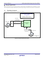
Figure 4-1 shows an example operating environment for the PMSC.
Periphral Mass Storage Class
Driver (PMSC)
+
USB Basic Peripheral Driver
USB Cable
Enumeration
(Control Transfer)
USB Host PC
USB
PORT
Bulk Data Communication
(Bulk Transfer)
USB
PORT
Evaluation
Board
User
Cable
Emulator
Emulator Cable
Emulator Host
PC
Figure 4-1 Example Operating Environment
R01AN2632EJ0100 Rev.1.00
Aug 21, 2015
Page 15 of 19
Renesas USB MCU
4.2
USB Peripheral Mass Storage Class Driver (PMSC)
Specifications
The sample application comprises two parts: initial settings and main loop.
The PMSC to process file write and file read to the storage area or the like to the request from the USB host. Therefore,
the sample application performs no processing on data transferred from the host and only periodically call the USB
driver.
Figure 4 2 shows a process flowchart of the sample application.
PMSC APL
(usbf_main)
Initial settings
(pmsc_registration)
(R_USB_Open)
(msc_init)
Main loop
(R_usb_pstd_poll)
(R_usb_pmsc_poll)
Figure 4-2 Flowchart
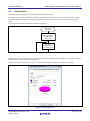
Sample application will be recognized as a removable disk when connected with the USB host. It is possible to perform
the data transfer, such as file reading and writing.
Figure 4-3 shows the operating screen of a PC connection.an example operating environment for the PMSC.
Figure 4-3 Operating screen
R01AN2632EJ0100 Rev.1.00
Aug 21, 2015
Page 16 of 19
Renesas USB MCU
4.3
USB Peripheral Mass Storage Class Driver (PMSC)
Initial settings
Sample settings are shown below.
void usbf_main(void)
{
/* Initial setting of USB driver (Refer to “4.3.1”) */
pmsc_registration();
/* Startup USB module (Refer to “4.3.2”) */
R_USB_Open();
/* Initial setting of Application (Refer to “4.3.3”) */
msc_init();
/* main loop */
while(1)
{
R_usb_pstd_poll();
R_usb_pmsc_poll();
}
}
4.3.1
Initial setting of USB driver
After specifying the necessary information in the members of the class driver registration structure (USB_PCDREG_t),
call R_usb_pstd_DriverRegistration() to register the class driver information for the USB-BASIC-F/W.
Pipe information table and descriptor information is described in r_usb_pmsc_descriptor.c.
Create each descriptor based on USB specification.
A sample of information specified in the structure declared by USB_PCDREG_t is shown below.
void pmsc_registration(void)
{
USB_PCDREG_t driver;
/* Structure for the class driver registration */
/* Pipe information table setting */
driver.pipetbl
= &usb_gpmsc_EpTbl[0];
/* Set the Device Descriptor table */
driver.devicetbl
= (uint8_t*)&usb_gpmsc_DeviceDescriptor;
/* Set the Qualifier Descriptor table */
driver.qualitbl
= (uint8_t*)&usb_gpmsc_QualifierDescriptor;
/* Set the Configuration Descriptor table */
driver.configtbl
= (uint8_t**)&usb_gpmsc_ConPtr;
// Note1
/* Set the Other Configuration Descriptor */
driver.othertbl
= (uint8_t**)&usb_gpmsc_ConPtrOther;
// Note1
/* Set the String Descriptor */
driver.stringtbl
= (uint8_t**)&usb_gpmsc_StrPtr;
// Note1
/* Set the function which is called when changing to the default state */
driver.devdefault = &msc_default;
/* Set the function which is called when completing the enumeration */
driver.devconfig
= &msc_configured;
/* Set the function which is called when disconnecting USB device */
driver.devdetach
= &msc_detach;
/* Set the function which is called when changing the suspend state */
driver.devsuspend = &msc_suspended;
/* Set the function which is called when resuming from the suspend state */
driver.devresume
= &msc_resume;
R01AN2632EJ0100 Rev.1.00
Aug 21, 2015
Page 17 of 19
Renesas USB MCU
USB Peripheral Mass Storage Class Driver (PMSC)
/* Set the function which is called when changing the interface */
driver.interface
= &R_usb_pmsc_SetInterface;
/* Set the function which is called when processing the control transfer
other than the standard request */
driver.ctrltrans
= &R_usb_pmsc_CtrlTrans;
/* Register the class driver information to PCD */
R_usb_pstd_DriverRegistration(&driver);
}
[Note]
1.
Set the start address of array which is set the descriptor start address in this member.
[Example]
uint8_t *usb_gpmsc_StrPtr[] =
{
usb_gpmsc_StringDescriptor0,
usb_gpmsc_StringDescriptor1,
usb_gpmsc_StringDescriptor2,
}
4.3.2
Startup USB module
Call the R_USB_Open() (API function of USB-BASIC-FW), set the USB module according to the initial setting
sequence of the hardware manual, the USB interrupt handler registration and USB interrupt enable setting.
4.3.3
Initial setting of application
The sample application uses the SDRAM area in the media area of the removable disk.
It is implemented by assigning a global variable(g_ramdisk_mem[RAMDISK_MEDIASIZE]) in the
file(r_ram_disk_format_data.c) to SDRAM area. If you want to change the media area, the memory arrangement in
accordance with the operating environment, please change the defined values MEDIA_ADDRESS (see Table 3-3).
The SDRAM area cleared to zero at software startup. Then it is FAT16 file system formatted by writing a global
variable(ram_disk_boot_sector[RAMDISK_SECTSIZE]) in file(r_ram_disk_format_data.c) to the top of the SDRAM
area.
R01AN2632EJ0100 Rev.1.00
Aug 21, 2015
Page 18 of 19
Renesas USB MCU
USB Peripheral Mass Storage Class Driver (PMSC)
Website and Support
Renesas Electronics Website
http://www.renesas.com/
Inquiries
http://www.renesas.com/contact/
All trademarks and registered trademarks are the property of their respective owners.
R01AN2632EJ0100 Rev.1.00
Aug 21, 2015
Page 19 of 19
Revision History
Rev.
1.00
Date
Aug 21, 2015
Description
Page
Summary
—
First edition issued
A-20
General Precautions in the Handling of Microprocessing Unit and Microcontroller Unit Products
The following usage notes are applicable to all Microprocessing unit and Microcontroller unit products from Renesas.
For detailed usage notes on the products covered by this document, refer to the relevant sections of the document as
well as any technical updates that have been issued for the products.
1. Handling of Unused Pins
Handle unused pins in accordance with the directions given under Handling of Unused Pins in the
manual.
The input pins of CMOS products are generally in the high-impedance state. In operation with an
unused pin in the open-circuit state, extra electromagnetic noise is induced in the vicinity of LSI, an
associated shoot-through current flows internally, and malfunctions occur due to the false
recognition of the pin state as an input signal become possible. Unused pins should be handled as
described under Handling of Unused Pins in the manual.
2. Processing at Power-on
The state of the product is undefined at the moment when power is supplied.
The states of internal circuits in the LSI are indeterminate and the states of register settings and
pins are undefined at the moment when power is supplied.
In a finished product where the reset signal is applied to the external reset pin, the states of pins
are not guaranteed from the moment when power is supplied until the reset process is completed.
In a similar way, the states of pins in a product that is reset by an on-chip power-on reset function
are not guaranteed from the moment when power is supplied until the power reaches the level at
which resetting has been specified.
3. Prohibition of Access to Reserved Addresses
Access to reserved addresses is prohibited.
The reserved addresses are provided for the possible future expansion of functions. Do not access
these addresses; the correct operation of LSI is not guaranteed if they are accessed.
4. Clock Signals
After applying a reset, only release the reset line after the operating clock signal has become stable.
When switching the clock signal during program execution, wait until the target clock signal has
stabilized.
When the clock signal is generated with an external resonator (or from an external oscillator)
during a reset, ensure that the reset line is only released after full stabilization of the clock signal.
Moreover, when switching to a clock signal produced with an external resonator (or by an external
oscillator) while program execution is in progress, wait until the target clock signal is stable.
5. Differences between Products
Before changing from one product to another, i.e. to a product with a different part number, confirm
that the change will not lead to problems.
The characteristics of Microprocessing unit or Microcontroller unit products in the same group but
having a different part number may differ in terms of the internal memory capacity, layout pattern,
and other factors, which can affect the ranges of electrical characteristics, such as characteristic
values, operating margins, immunity to noise, and amount of radiated noise. When changing to a
product with a different part number, implement a system-evaluation test for the given product.
Notice
1.
Descriptions of circuits, software and other related information in this document are provided only to illustrate the operation of semiconductor products and application examples. You are fully responsible for
the incorporation of these circuits, software, and information in the design of your equipment. Renesas Electronics assumes no responsibility for any losses incurred by you or third parties arising from the
use of these circuits, software, or information.
2.
Renesas Electronics has used reasonable care in preparing the information included in this document, but Renesas Electronics does not warrant that such information is error free. Renesas Electronics
3.
Renesas Electronics does not assume any liability for infringement of patents, copyrights, or other intellectual property rights of third parties by or arising from the use of Renesas Electronics products or
assumes no liability whatsoever for any damages incurred by you resulting from errors in or omissions from the information included herein.
technical information described in this document. No license, express, implied or otherwise, is granted hereby under any patents, copyrights or other intellectual property rights of Renesas Electronics or
others.
4.
You should not alter, modify, copy, or otherwise misappropriate any Renesas Electronics product, whether in whole or in part. Renesas Electronics assumes no responsibility for any losses incurred by you or
5.
Renesas Electronics products are classified according to the following two quality grades: "Standard" and "High Quality". The recommended applications for each Renesas Electronics product depends on
third parties arising from such alteration, modification, copy or otherwise misappropriation of Renesas Electronics product.
the product's quality grade, as indicated below.
"Standard": Computers; office equipment; communications equipment; test and measurement equipment; audio and visual equipment; home electronic appliances; machine tools; personal electronic
equipment; and industrial robots etc.
"High Quality": Transportation equipment (automobiles, trains, ships, etc.); traffic control systems; anti-disaster systems; anti-crime systems; and safety equipment etc.
Renesas Electronics products are neither intended nor authorized for use in products or systems that may pose a direct threat to human life or bodily injury (artificial life support devices or systems, surgical
implantations etc.), or may cause serious property damages (nuclear reactor control systems, military equipment etc.). You must check the quality grade of each Renesas Electronics product before using it
in a particular application. You may not use any Renesas Electronics product for any application for which it is not intended. Renesas Electronics shall not be in any way liable for any damages or losses
incurred by you or third parties arising from the use of any Renesas Electronics product for which the product is not intended by Renesas Electronics.
6.
You should use the Renesas Electronics products described in this document within the range specified by Renesas Electronics, especially with respect to the maximum rating, operating supply voltage
range, movement power voltage range, heat radiation characteristics, installation and other product characteristics. Renesas Electronics shall have no liability for malfunctions or damages arising out of the
use of Renesas Electronics products beyond such specified ranges.
7.
Although Renesas Electronics endeavors to improve the quality and reliability of its products, semiconductor products have specific characteristics such as the occurrence of failure at a certain rate and
malfunctions under certain use conditions. Further, Renesas Electronics products are not subject to radiation resistance design. Please be sure to implement safety measures to guard them against the
possibility of physical injury, and injury or damage caused by fire in the event of the failure of a Renesas Electronics product, such as safety design for hardware and software including but not limited to
redundancy, fire control and malfunction prevention, appropriate treatment for aging degradation or any other appropriate measures. Because the evaluation of microcomputer software alone is very difficult,
please evaluate the safety of the final products or systems manufactured by you.
8.
Please contact a Renesas Electronics sales office for details as to environmental matters such as the environmental compatibility of each Renesas Electronics product. Please use Renesas Electronics
products in compliance with all applicable laws and regulations that regulate the inclusion or use of controlled substances, including without limitation, the EU RoHS Directive. Renesas Electronics assumes
no liability for damages or losses occurring as a result of your noncompliance with applicable laws and regulations.
9.
Renesas Electronics products and technology may not be used for or incorporated into any products or systems whose manufacture, use, or sale is prohibited under any applicable domestic or foreign laws or
regulations. You should not use Renesas Electronics products or technology described in this document for any purpose relating to military applications or use by the military, including but not limited to the
development of weapons of mass destruction. When exporting the Renesas Electronics products or technology described in this document, you should comply with the applicable export control laws and
regulations and follow the procedures required by such laws and regulations.
10. It is the responsibility of the buyer or distributor of Renesas Electronics products, who distributes, disposes of, or otherwise places the product with a third party, to notify such third party in advance of the
contents and conditions set forth in this document, Renesas Electronics assumes no responsibility for any losses incurred by you or third parties as a result of unauthorized use of Renesas Electronics
products.
11. This document may not be reproduced or duplicated in any form, in whole or in part, without prior written consent of Renesas Electronics.
12. Please contact a Renesas Electronics sales office if you have any questions regarding the information contained in this document or Renesas Electronics products, or if you have any other inquiries.
(Note 1)
"Renesas Electronics" as used in this document means Renesas Electronics Corporation and also includes its majority-owned subsidiaries.
(Note 2)
"Renesas Electronics product(s)" means any product developed or manufactured by or for Renesas Electronics.
http://www.renesas.com
SALES OFFICES
Refer to "http://www.renesas.com/" for the latest and detailed information.
Renesas Electronics America Inc.
2801 Scott Boulevard Santa Clara, CA 95050-2549, U.S.A.
Tel: +1-408-588-6000, Fax: +1-408-588-6130
Renesas Electronics Canada Limited
9251 Yonge Street, Suite 8309 Richmond Hill, Ontario Canada L4C 9T3
Tel: +1-905-237-2004
Renesas Electronics Europe Limited
Dukes Meadow, Millboard Road, Bourne End, Buckinghamshire, SL8 5FH, U.K
Tel: +44-1628-585-100, Fax: +44-1628-585-900
Renesas Electronics Europe GmbH
Arcadiastrasse 10, 40472 Düsseldorf, Germany
Tel: +49-211-6503-0, Fax: +49-211-6503-1327
Renesas Electronics (China) Co., Ltd.
Room 1709, Quantum Plaza, No.27 ZhiChunLu Haidian District, Beijing 100191, P.R.China
Tel: +86-10-8235-1155, Fax: +86-10-8235-7679
Renesas Electronics (Shanghai) Co., Ltd.
Unit 301, Tower A, Central Towers, 555 Langao Road, Putuo District, Shanghai, P. R. China 200333
Tel: +86-21-2226-0888, Fax: +86-21-2226-0999
Renesas Electronics Hong Kong Limited
Unit 1601-1611, 16/F., Tower 2, Grand Century Place, 193 Prince Edward Road West, Mongkok, Kowloon, Hong Kong
Tel: +852-2265-6688, Fax: +852 2886-9022
Renesas Electronics Taiwan Co., Ltd.
13F, No. 363, Fu Shing North Road, Taipei 10543, Taiwan
Tel: +886-2-8175-9600, Fax: +886 2-8175-9670
Renesas Electronics Singapore Pte. Ltd.
80 Bendemeer Road, Unit #06-02 Hyflux Innovation Centre, Singapore 339949
Tel: +65-6213-0200, Fax: +65-6213-0300
Renesas Electronics Malaysia Sdn.Bhd.
Unit 1207, Block B, Menara Amcorp, Amcorp Trade Centre, No. 18, Jln Persiaran Barat, 46050 Petaling Jaya, Selangor Darul Ehsan, Malaysia
Tel: +60-3-7955-9390, Fax: +60-3-7955-9510
Renesas Electronics India Pvt. Ltd.
No.777C, 100 Feet Road, HALII Stage, Indiranagar, Bangalore, India
Tel: +91-80-67208700, Fax: +91-80-67208777
Renesas Electronics Korea Co., Ltd.
12F., 234 Teheran-ro, Gangnam-Gu, Seoul, 135-080, Korea
Tel: +82-2-558-3737, Fax: +82-2-558-5141
© 2015 Renesas Electronics Corporation. All rights reserved.
Colophon 5.0