1
US006496222B1
(12) United States Patent
(10) Patent N0.:
(45) Date of Patent:
Roberts et al.
(54)
DIGITAL CAMERA WITH MEMORY
FORMAT INITIALIZATION
US 6,496,222 B1
*Dec. 17, 2002
9/1979 Dischert et al.
4,167,022 A
4,385,361 A
5/1983 Moates
(List continued on neXt page.)
(75) Inventors: Marc K. Roberts, Burke, VA (US);
Matthew A. Chikosky, Spring?eld, VA
FOREIGN PATENT DOCUMENTS
(US); Jerry A. Speasl, Vienna, VA
DE
EP
EP
EP
EP
(Us)
(73) Assignee: St. Clair Intellectual Property
Consultants, Inc., Grosse Pointe, MI
(Us)
3809677
0105213
903030765
0371961
0218291
A1
A2
A2
B1
3/1988
4/1984
3/1990
6/1990
3/1991
(List continued on neXt page.)
Notice:
Subject to any disclaimer, the term of this
patent is extended or adjusted under 35
U.S.C. 154(b) by 0 days.
OTHER PUBLICATIONS
Izawa et al.*
This patent is subject to a terminal dis
claimer.
(21) Appl. No.: 09/724,375
Nov. 27, 2000
(22) Filed:
EIKONIX (Sep. 29, 1988).*
“Camera Stores Images On Chips”, Laser Focus World, Apr.
1990, pp. 72, 74 and 75.
“Should I Sell Now? Follow the Trends”, CompuServe
Magazine, at 30 (Nov. 1991), Robert Cullen.
“Apple Planning to Announce 68030 Version of MacII”,
Info World, vol. 10, No. 38 (Sep. 5, 1988), Laurie Flynn, et
al.
Related U.S. Application Data
“Digital Card Camera”, ITEJ Technical Report, vol. 14, No.
(63)
Continuation of application No. 09/253,831, ?led on Feb.
19, 1999, now Pat. No. 6,233,010, which is a continuation
of application No. 08/712,493, ?led on Sep. 11, 1996, which
5, at 7 (Jan. 1990), Fujimori et al. (no translation).
“Graphics Formats”, Byte, at 305 (Sep. 1989), Gerald L.
Graef.
is a continuation of application No. 08/098,787, ?led on Jul.
29, 1993, now Pat. No. 5,576,757, which is a continuation
“Directory Assistance”, Byte, at 327 (Jun. 1989), Rick
of application No. 07/878,603, ?led on May 5, 1992, now
Grehan.
abandoned, which is a continuation of application No.
07/615,848, ?led on Nov. 20, 1990, now Pat. No. 5,138,459.
(51)
(52)
(58)
(List continued on neXt page.)
Int. Cl.7 ................................................ .. H04N 5/76
Primary Examiner—Tuan Ho
U.S. Cl. ...................... .. 348/231; 348/220; 348/207
Field of Search ............................... .. 348/207, 220,
(74) Attorney, Agent, or Firm—Harness, Dickey & Pierce,
348/221, 222, 231, 232, 233, 373; 386/117,
118; H04N 5/225
U.S. PATENT DOCUMENTS
4,074,324 A
4,118,687 A
4,131,919 A
(57)
ABSTRACT
Adigital camera includes a digital memory system having a
control unit for checking for proper format initialization of
a removable digital memory element and for performing
format initialization of the memory element when necessary.
References Cited
(56)
P.L.C.
2/1978 Barrett
10/1978 McWaters et al.
12 Claims, 11 Drawing Sheets
12/1978 Lloyd et al.
SPEED
15
16
F25 F1000
FLASH
+v
2
,1
/ 19
+V
ENABLE &
FORMAT
IBM APPLE
/
22
I
+v HALF
FRAME
+V
LOW COLOR
COUNTER
& STATUS
INDICATOR
HIGH
I
MED
SELF
\
:
‘
2°
LINES
+V FULL
TEST
CPU
ADDRESS &
CONTROL
RANGE
CONTROL
FAILURE
1y
& ADDRESS
DECODER
FOCUS &
1,
LINES
FUNCTION
DATA LINES
\— +v
21
1'0-13
DATA
EXPOSURE
CONTROL
17
78a
/
‘T SHUTTER é.
SHOOT
T0
9
___
2a
1
DISK
\
FORMAT =7:
ERROR
RESOLUTION
SWITCH
+V
BLACK 81
WHITE
\ 14B
MODE
SWITCH
US 6,496,222 B1
Page 2
US. PATENT DOCUMENTS
4,420,773
4,453,268
4,456,931
4,541,021
4,571,638
4,577,239
4,587,633
4,614,977
4,641,203
4,656,524
4,656,525
4,682,248
4,689,696
4,691,253
4,701,805
4,706,126
4,714,962
4,730,222
4,739,400
4,758,883
4,760,606
A
A
A
A
A
A
A
A
A
A
A
A
A
A
A
A
A
A
A
A
A
12/1983
6/1984
6/1984
9/1985
2/1986
3/1986
5/1986
9/1986
2/1987
4/1987
4/1987
7/1987
8/1987
9/1987
10/1987
11/1987
12/1987
3/1988
4/1988
7/1988
7/1988
8/1988
8/1988
9/1988
9/1988
11/1988
4,763,204 A
4,768,110 A
4,772,956 A
4,774,600 A
4,782,399 A
4,803,554 A
4,817,050
4,821,121
4,827,347
4,829,383
4,837,628
4,847,677
4,855,779
4,858,032
4,872,054
4,876,590
4,887,161
4,897,732
4,903,132
4,905,092
4,907,231
4,914,746
4,935,821
4,943,850
4,947,271
4,963,986
4,967,297
4,972,266
4,974,197
4,982,291
4,992,886
4,994,912
4,999,715
5,006,937
2/1989 Pane
A
A
A
A
A
A
A
A
A
A
A
A
A
A
A
A
A
A
A
A
A
A
A
A
A
A
A
A
5,016,107 A
3/1989
4/1989
5/1989
5/1989
6/1989
7/1989
8/1989
8/1989
10/1989
10/1989
12/1989
1/1990
2/1990
2/1990
3/1990
4/1990
6/1990
7/1990
8/1990
10/1990
10/1990
11/1990
11/1990
1/1991
2/1991
2/1991
3/1991
4/1991
*
2 *
,
,
5,027,214 A
Toyoda et al.
Britt
Toyoda et al.
Konishi et al.
Schneider et al.
$911899
Wang et 91Kawahara et al.
Miller
Norris et al.
Norris
Schwartz
Plummer
Silver
Maeshima
Kondo
Levine
Schauffele
Veitch
Kawahara et al.
Lesnick et al.
Kinoshita et al.
Dunlap et al.
Roche et al.
Baumeister
Sato
5,065,246
5,067,029
5,068,744
5,077,612
5,091,747
5,097,344
5,099,846
5,105,284
5,111,283
5,111,288
5,119,081
5,130,813
5,153,730
5,164,831
5,170,262
5,212,770
5,214,781
A
A
A
A
A
A
A
A
A
A
A
A
A
A
A
A
A
11/1991
11/1991
11/1991
12/1991
2/1992
3/1992
3/1992
4/1992
5/1992
5/1992
6/1992
7/1992
10/1992
11/1992
12/1992
5/1993
5/1993
Takemoto et al.
Takahashi
Ito
Megrgardt et a1.
Tsai
Aoki et a1_
Hardy
Sakata et a1.
Nagasawa et a1.
Blackshear
Ikehira
Oie et aL
Nagasaki et a1.
Kuchta et a1.
Kinoshita et a1.
Smith et a1.
Miki et aL
5,218,455
5,227,863
5,231,501
5,231,549
5,241,659
5280397
5287266
5301262
5,321,831
5,379,376
5,454,067
A
A
A
A
A
A
A
A
A
A
A
6/1993
7/1993
7/1993
7/1993
8/1993
1/1994
2/1994
4/1994
6/1994
1/1995
9/1995
Kristy
Bilbrey et a1.
Sakai
Morehouse et a1.
Parulski et a1_
Rhodes
Malec et aL
Kashiwagi
Hirose
Bednowitz
Tsai
5,454,096 A
Komatsu et al.
Beaulier
Bell
Hams? er 91Sasakl
Music er 91Ishikawa er 91Okada et a1.
Gray et al.
Parulski
Watanabe et al.
Kinoshita et al.
Yamawaki
Koshiishi et al.
Watanabe et al.
Nishi et al.
Sano et al.
Asaida
Nakayama et al.
Fukyuama et al.
Okita et al.
Tani
Blount et al.
Kurahashi et al.
Klappert
Lumelsky et al.
Porcellio et al.
Nonoshita et a1.
5,475,539
5,661,823
5,724,101
5,764,286
5,822,082
6,020,982
2001/0033734
A
A
A
A
A
A
A1
*
9/1995 Otsuka et a1. ............ .. 395/401
12/1995
8/1997
3/1998
6/1998
10/1998
2/2000
10/2001
Orii
Yamauchi et a1.
Haskin
Kawamura et a1.
Sato et a1.
Yamauchi et a1.
Hoda et a1.
FOREIGN PATENT DOCUMENTS
EP
EP
JP
JP
JP
JP
JP
JP
JP
JP
JP
JP
JP
JP
0156923 B1
0390421 B1
61-269565
62-237341
63-45760
63-284987
A 64-060071
2-125572
2-172382
2-183675
A 02-186882
2-202782
A02-211780
2-222385
12/1993
7/1994
11/1986
10/1987
2/1988
11/1988
3/1989
5/1990
7/1990
7/1990
7/1990
8/1990
8/1990
9/1990
JP
WO
2-257780
90/09717
10/1990
8/1990
OTHER PUBLICATIONS
5/1991 Sasson et al.
sssiiki it ali 1
a ana
6/1991 Fujimori
e e
a .
“Picture Recording and Electric Power Consumption”,
~
~
~
~
-
Shashrrn Kogyo, at 94 (Apr. 1988), Surnihisa Hashiguchi.
5,027,221 A
6/1991 Hisatake et al.
“Possibilities of the Digital Electronic Still Carnera”,
5,029,115 A
7/1991 Geraci
Shashin Kogaku, at 110 (Feb. 1988), Surnihisa Hashiguchi.
,
,
2
5,032,930 A
Z1991
Ota et al'
/1991 Watanabe et al.
“MacDOSsier,
Tearing Down The Walls. Between
Macs and
,,
.
7/1991 Suetaka et a1_
PCs , MacWorld, at 165 (Jul. 1990), Jun Herd.
5,034,804 A * 7/ 1991 Susaki et al5JO35J633 A
7/1991 Kobayashi et a1~
5938392 A
8/1991 Moms ,et a1‘
5,040,068 A
“Swallowing Planets; Today’s Feeding Frenzy of Data Cap
ture”, Journal of Electronic Defense, vol. 12, No. 10, at 109
(Oct. 1989), Sheldon B. HerskovitZ.
8/ 1991 Parulski et al.
5,058,185 A
10/1991 Morris et a1_
“Desktop Video On The Arniga”, Electronic Learning, vol.
5,060,069 A
10/1991 Aoki
8, No. 2, at 54 (Oct. 1988), Lanny HertZberg.
US 6,496,222 B1
Page 3
“ImagingAVampire; SofWare Review‘ Evaluation Of Three
“Photos Go Electronic: NeW Standard Pulls Images Into
MSDOS—Based Image Processing Software Packages, ESD;
Computer Age”, High Technology Business, vol. 8, No. 2; at
15 (Feb. 1988), Robert Wood.
“AGA Thermovision Digital Image Processing System”, by
AGA Infrared Systems AB (1982).
The Electronic System Design Magazine, vol. 19, No. 10, at
63 (Oct. 1989), Steven J. Hollinger.
“Marketing through Innovation, Photonics at Work”, Pho
tonics Spectra, vol. 23, No. 7, at 66 (Jul. 1989), Herbert
Kaplan.
Photoshop and Color Sudio: Mac Image Manipulation
Tools, InfoWorld, at 118 (Jan. 29, 1990), Michael Miller.
“Digital Still Video Camera Using Semiconductor Memory
Card”, IEEE 1989, at 184 (1989), IZaWa, et al.
“Logitech Debuts Digital Camera”, Government Computer
NeWs, vol. 10, No. 19 (Sep. 16, 1991), Cynthia Morgan.
“TIFF File Format”, The C GaZette, vol. 5, No. 2, at 27
“AGA Thermovision OSCAR —Pericolor System —Product
Information”, by AGA Infrared Systems AB (Copyright
1980).
“Agema Product Speci?cation —TIC—8000 With CATS, A
Complete HardWare/SoftWare Package For Thermal Analy
sis”, by Agema Infrared Systems (1986).
Apple SuperDrive: User Guide, http://docs.info.apple.com/
article.html?artnum—4545
http://docs.info.apple.com/ar
ticle.html?artnum—4546 http://docs.info.apple.com/article
(Winter 1990—1991), James Murray.
.html?artnum—4547 (Aug. 2, 1989), Apple Computer, Inc.
“Solid—State Electronic Still Camera Memory Card Sys
tem”, ITEJ 1989, at 193—194, NakagaWa, et al. (no transla
Canon XapShot RC250 Manual (1988).
Canvas 2.0 softWare.
tion).
Canvas 2.0 Upgrade Manual, at v. (1988), Levy et al,
Deneba Systems, Inc.
CompuServe Financial Services User’s Guide, at 4—10 (Jul.
13, No. 22,.at 11 (Mar. 1989), Ochi, et al. (no translation).
CompuServe Information Manager User Guide, at 115, 121,
“Digital Still Camera System”, ITEJ Technical Report, vol.
14, No. 5, at 13 (Jan. 1990), Nishi, et al. (no translation).
“Card Camera ‘FUJIX DS—IP’”, ITEJ Technical Report, vol.
1988), CompuServe Incorporated.
“State Of The Art For The 90’s Office”, Appliance Manu
172, 182, 183 (Nov. 1989), CompuServe Incorporated.
facturer, vol. 37, No. 1, at 76 (Jan. 1989), Norman Remich.
“Highlights From Digital 90 Trade ShoW”, Editor & Pub
lisher, vol. 123, No. 7, at 42P (Feb. 24, 1990), Jim Rosen
CompuServe Information Service, VIDTEX 4.0 Standards
for Terminal Emulator Programs (Apr. 1985), CompuServe
Incorporated.
berg.
“Curtis Inc. Announces NeW Prices And NeW ROMDISK
“Dycam Model I the ‘?rst portable digital still camera’”,
MacWEEK, vol. 4, No. 35, at 34 (Oct. 16, 1990), Carolyn
Models”, NeW Release (Jan. 4, 1988), Curtis, Inc.
Said.
No. 4 (Apr. 1990).
“Camera Uses E2 PROM Film”, Electronic Engineering
“Digital Back For Medium—Format Rollei Cameras”, Editor
& Publisher, vol. 124, No. 8, at 23P (Feb. 23, 1991).
“Digital Camera —The Path To The Present”, by Japan
Times, at 45 (Apr. 10, 1989), Miyoko Sakurai.
“Picture Coding For Digital Still Camera”, Toshiba RevieW,
DataviZ “MacLink Plus” Advertisement, MacWorld, vol. 7,
vol. 45, No. 8, at 635 and 638 (1990), Sasaki (no transla
Camera Museum (Oct. 24, 2000) (no translation).
tion).
DRAW, a Hi—Res DraWing Program by Micro—Labs, Inc.
“Dycam premiers still—video camera”, MacWEEK, Vol. 4,
No. 11, at 27 (Mar. 20, 1990), Carolyn Said.
“Camera Uses E2 PROM Film”, Electronic Engineering
Times, at 45 (Apr. 10, 1989), Miyoko Sakurai.
“Picture Coding For Digital Still Camera”, Toshiba RevieW,
vol. 45, No. 8, at 635 and 638 (1990), Sasaki (no transla
tion).
Digital Electronic Still Camera System, ITEJ Technical
Report, vol. 13, No. 22, at 17 (Mar. 1989), Sasaki, et al. (no
(1984).
“Fuji?lm Brings The Digital Camera Ds—7 With Convenient
SmartMedia Storage To The Consumer Market”, http://
WWW.fuji?lm.co.jp/eng/salon/pkna/digi—l.html (Sep. 18,
1996).
FujiX Digital Still Video Camera DS—IP, Fuji Photo Film
Co., Ltd (1988).
FUJIX DS—X user’s manual (1991).
Graphics Interchange Format (GIF) Speci?cation, pp. 1—18,
translation).
CompuServe (Jun. 15, 1987).
“NoW And Future Of Electronic Still Camera”, 1990 Joint
Convention Record of Institutes of Electrical and Informa
puServe (Jul. 31, 1990).
tion Engineers, Japan (Aug. 28—30, 1990) Sasaki et al. (no
Heat Made Visible —The World of Infrared, by Agema
translation).
“Graphics PoWer For The Rest Of Us”, PC World, at 164
Graphics Interchange Format, Version 89a, pp. 1—42, Com
Infrared Systems (1989).
HMI Protocol De?nition Document, Remote Terminal Inter
(Nov. 1990), Mike Smith—Heimer, et al.
rogation Sequence 1.10.2, at 1.
“Digital Still Camera For Business Use”, Electronics Life, at
IBM Disk Operating System Version 3.3 User’s Guide and
84 (Apr. 1990), Someya (no translation).
Reference, First Edition (Apr. 1987).
“Photoshop is Picture—Perfect”, Byte, at 103 (Apr. 1990),
Tom Thompson.
Dempa Daily NeWspaper Technical Report (Mar. 30, 1989).
“IC Card Camera System —Toshiba & Fuji Photo Film”,
“Freelance Masters OS/2”, PC World, at 85 (Nov. 1990),
Inside Macintosh Volume V by Apple Computer, at V—85 to
John Walkenbach.
V—115 (Jan. 1988).
“OvervieW Of The Jpeg (ISO/CCITT) Still Image Compres
sion Standard”, SPIE, vol. 1244 Image Processing Algo
Macintosh MacPaint Manual, Apple Computer, Inc. (1983).
Macintosh Manual (1984).
“Maintenance Technology —Infrared Thermography”Agema
rithms and Techniques, at 220 (1990), Gregory Wallace.
“A Bit Rate Controlled Dci Compression Algorithm For
Digital Still Camera”, Proc. of SPIE —The International
Society for Optical Engineering, vol. 1244 at 234 (Feb.
12—14, 1990), Watanabe, et al.
Infrared Systems (Nov. 1989).
Microsoft MS—DOS User’s Guide Version 3.3, Microsoft
Corporation (1987).
MS—DOS 4.0.
US 6,496,222 B1
Page 4
“Palmtop Computer Sales Soar”, The Atari Report, vol. 3,
No. 1, at 5 (of printout), Atari Corporation (Spring 1990).
Thermovision 470 Technical Speci?cation, Thermovision
400 Series Operating Manual, AGEMA Infrared Systems
PhotoMac, User Manual, at 105—106, Avalon Development
Group, (1988), EWart et al.
Prototype Announcement, FujiX DS—IP digital still camera,
AB (1989).
Fuji Photo Film Co., Ltd., Fuji News (Sep. 20, 1988).
Macintosh IIX OWner’s Guide (1988).
“Reviews: Adome Photoshop 1.0”, MacWorld, vol. 7, No. 6,
at 186 (Jun. 1990).
Macintosh SE With FDHD (SuperDrive).
SLIDESHOW, a RAPIDOS Software by Rapidynamic Soft
Ware, Inc., licensed to Micro—Labs (1984).
(Jun. 1993), Samuel D. Holland, et al.
“Still Videos, Anyone?”, IEEE Spectrum, at 41 (Feb. 1990).
“The Atari Portfolio Palmtop”, http://WWW.atari—history
.com/computers/pccomputers/portfolio.html (1989).
NASA Tech Briefs, Digital Electronic Still Camera, at 30
“Still Video —Still Here?”, Electronics World & Wireless
World, at 873 (Oct. 1990), George Cole.
Thermovision 400 Series Operating Manual, by Agema
Macintosh System SoftWare User’s Guide Version 6.0
Infrared Systems (1991).
(1988).
“Thermovision 470 Information —Thermovision 470 Sys
tem”, by Agema Infrared Systems (1989).
Thermovision 800 Series Burst Recording Unit —Burst
Recording Unit, by Agema Infrared Systems (1989).
Personal Vision Live Video/Frame Grabber for Macintosh II
(1989).
TIC—8000 With CATS E The Complete HardWare/SoftWare
“StuffIt”, Macuser, at 77 (Dec. 1988).
Apple II System Utilities Manual, Apple Computer, Inc.
Package For Thermal Analysis, by Agema Infrared Systems
(1985).
TIC—8000 With CATS E —Thermovision 800 Series
(1988).
BountyQuest Digital camera With PC—compatible output
format Bounty, http://WWW.bountyquest.com/bounties/dis
playBounty.php?bounty Name=1121, Bounty Quest Corp.,
Inc. (2002—02).
Apple IIGS System SoftWare User’s Guide, Version 5.0,
Chapter 2 and Chapter 6.
* cited by examiner
U.S. Patent
Dec. 17, 2002
Sheet 1 0f 11
US 6,496,222 B1
1a/'\
SIGNAL
1MAGE§—>
TEMPORARY
‘IPROCESSOR
I/O
sTORAGE ’
I CCD
i OPTICs
‘_
v
SHUTTER,
4
EXPOSURE,
‘
& FOCUS
i
_
CONTROL
'
MASS MEMORY
CIRCLIITRY
r23
'
v
CONTROL
DEVICE
L—-—
\
3a\_7———'
I
5a
48
CONTROL PANEL
'
PRIOR ART
POWER
FIG,1
"‘_
_'
SUPPLY
\
PIXEL FRAME COMPRESSION
BUFFER BUFFER PROCESSOR
f
1
>—>L
IMAGE
P7
a
I
‘L
To
K
4‘
11-)
—>-
12 7
[13
J
—>
<
CCO
PIxEL
A/O
OPTIcs MULTIPLEXER CONVERTERS
L.
I
‘
f‘ 2
V
DISK I/O
f9
INTERFACE
‘
v
I
CONTROL
_I
5
DIGITAL CONTROL
PANEL
UNIT
L--\
A
14
4
If
\
[17
DISK DRIVE
POWER
-<--
SUPPLY
ASSEMBLY
——>
*I
OPERATOR VARIABLE
CONTROL SWITCHES
FIG. 2
U.S. Patent
Dec. 17, 2002
Sheet 2 0f 11
US 6,496,222 B1
567
/AUDIO F125 INFO DATA
\
l
K I 23
I
(
w
\
1
!
__
AUDIO DATA
_
_
(CNEXT FILE)
53\
@TAGE FILE INFO DATA
,
I 2!
‘
ll
z
‘
l
* i T
w
\
,
IBM =o1j/ coLoR=1jJ
KoTHER=10
52b
‘
55
B & w=0
TRACKS 51a 53
NEXT
i— IMAGE DATA?CIMAGE
a a “ a
57/ 54
FORMAT
APPLE=00\5
A
//
PM
U.S. Patent
Dec. 17, 2002
POWER-ON SENSOR
Sheet 3 0f 11
US 6,496,222 B1
(AID
ACTIVE
.
. DISK SNSERT
RESET
NITIATE SELF TEST
DiSPLAY C/ P
DlAGNOSTECS
DIAGNOSTlCS
CHECK
Y
CHECK D [SK
SPACE
ABNORMAL
NORMAL
POWER
F RESET FRAME COUNTER I
SUPPLY
OUTPUT
ABNORMAL
CHECK DISK
'
NORMAL
{READ SWITCH SETTINGS]
DRIVE
ARM FLASH a‘ EXPOSURE
CHCUITS
ABNORMAL
PERFORM CPU
NORMAL
DIAGNOSTICS
L
.
ACTIVATE BACKGROUND
DiAGNOSTICS
CHECK
NORMAL
ABNORMAL [
pé?fllf
@
ABNORMAL
PERFORM 1/0
olAsNosTics
SYSTEM READY
Di
= NoRMAL
@)
LOOK-UP ERROR
CODE & DiSPLAY
l
WAIT FOR
RESET
NORMAL
@
FIG. 3
l
U.S. Patent
Dec. 17, 2002
Sheet 4 0f 11
US 6,496,222 B1
PIXEL
FIG. 5 A
r7
1B
PIXEL
SE
82
s/H
_
“AADj/z
1
féo p:
S/H
/
I
AID
_ 8
7/2:
l:
‘2
-
.
so
FIST
I
CE
ADDRESS &
coNTRoL LINEs
cc
RST
PB
RsT
FBI
FIST
I Y
AO-A32 DO-D18
TO ocu
9
780 was
.1
A".
D ,3,
Q
Z
CE
1k 22.":
If 24
PIXEL SELECT 7?
SE -n__-—-II
SAMPLE ENABLEv
'
A10 coNvERT
ENABLE
cc __I_I___
3.;
;
;. _5
5 480 PIxELs
I;;
;1
coNvERT
‘
vERTIcAL ADDRESS
,,
1)?
COMPLETE
so
I I
7y
PIXEL BUFFER
" HORIZONTAL ADDRESS
& coNTRoL LINEs
SAMPLE CLEAR-e8
P8
6‘ CONTROL LINES
ENABLE
HST
I I
I
PB ___J1j,2
FRAME BUFFER
ENABLE
HR 58
sIoN
PRocEssoR
‘
PC
I
coM Tos
PRE
A5”?
..~_-—,s‘1
;$E
-
,
:">.MULTl- 78E cco ARRAY
FRAME
BUFFER BUFFER
10A
11\
.FUU'LFUULILI
CLOCK
U.S. Patent
Dec. 17,2002
SPEED
FLASH
+v
15
f SH
FLA
f?
H
19
CONTROL
+v
ENABLE 8‘
FUNCTION 3;;
FRAME
cOuNTER
& sTATus
23
1
SELF
\
DISK
\
TEsT
?
a
CCEQTEQOL
20
+V
LOW COLOR
HIGH
INDICATOR
g,
+V
BLACK &
'
MED 1 14A
FORMAT ?
FAILURE
ADDRESS & _/
-—~
21
CPU
OEcOOER "7:
22
I
\\
& AOOREss
/
RANGE
LINES
/
DATA L'NES
+v HALF
10-13
DATA
ExPOsuRE
+v FULL
7 , Taoat
/9
EC: sHuTTER & ———4
CONTROL
US 6,496,222 B1
16
F25 F1000
I
Sheet 5 0f 11
ERROR
WHITE
l
'\14s
RESOLUTION
MODE
SWITCH
:swlTcH
FIG. 6
512-BYTE
HEAOER
60a
‘14A
plcSlZE
LOW
pIcFRAME
-_5_
+\/
MED
'
_\
ss
OPCODE
-—O
HIGH
PICTURE OATA
-;i—
60b
_
}_
OPCODE
'
FIG. 6A
PICTURE OATA
FIG.6B
END OF PICTURE
U.S. Patent
Dec. 17, 2002
Sheet 6 6f 11
F
'SHOOT' 6
h J
2
5
33
i
31
US 6,496,222 B1
REMOTE
_.
REMOTE
\
CAMERA JACK
FIxED DELAY
+V
J
v
+
COMMAND !
'
. S . q .
|
L
FUL
+v HALF
. ..
'
RELAY
30 —/l?
+V
SWITCH
32
+V
CAMERA BODY /
TO/FROM
FIG' 6C
COMPRESSION 12
PROCESSOR
‘‘
‘YO/FROM
FRAME
A‘
“:mm’“
f9
I
ENABLE &
=
CONTROL LINES
-
7
RAM’
;
BUFFER —
11
‘
ROM
MEMORY
/ 24
A
FUNCTION & /‘9
ADDRESS
4
Bo
DECODER
TO/FROM
___|
/
I
CONTROL
PANEL
ADDRESS
2
& DATA
LINES
2o
,CPU
p AUXILIARY I/O
TO
»
2s
INTERFACE
‘ V
DISI< l/O lNTERFACE-\.13
A
TO/FROM Y s
DIsI< DRIVE ASSEMBLY
FIG. 7
U.S. Patent
Dec. 17, 2002
US 6,496,222 B1
Sheet 7 of 11
FRAME BUFFER
INPUT IMAGE FRAME
Y
RG8 TO
FROM 10
PIXEL BUFFER
CHROMINANCE/LUMINANCE
CONVERSION
r8112“
--—>/:7\
:7
Y
MOST RECENT
IMAGE FRAME
PERFORM DISCRETE
COSINE TRANSFORM
(DCTI
(LAST)
I
FIRST IMAGE
FORMAT OUTPUT
COEFFICIENTS
:
C:
IMAGE
g "‘? FRAMES
i!
I
FRAME
- '->TO 12
COMPRESSION
I
——-_—>
PROCESSOR
RAM MEMORY
PERFORM HUFFMAN
CODING
FIG. 13
Y
PERFORM OUTPUT
FORMATTING
I
OUTPUT COMPRESSED
IMAGE TO MEMORY
FIG. 8
-» E
E5
Commercial Video Diskette Video Format
Still Video (Analog format)
Camera
Diskette
Translator (Digital format)
FIG. 10
PC
U.S. Patent
Dec. 17, 2002
Sheet 9 0f 11
US 6,496,222 B1
INITIALIZE I/O & READ DISK
CHECK DISK
BOOT SECTOR
FORMATTED
NOT
FORMATTED
I
READ DISK SIZE AND TYPE
Y
DISPLAY NOT FORMATTED
CODE
POLL CONTROL PANEL
FORMAT SETTINGS
I
V
HANG UNTIL FORMAT
MODE SELECT
I
POLL CONTROL PANEL
FORMAT SETTINGS
Y
LOOK-UP APPROPRIATE
DOES DISK
FORMAT AGREE
NO
DISPLAY
WITH C/P
ERROR
SETTING?
CODE
d)
é) YES
1
FORMAT UTILITY AND OS I DISPLAY ‘ FORMAT CODE
Y
PERFORM FORMAT
INITIALIZATION
@
Y
DISPLAY FRAME
STORAGE CAPACITY
I
[HANG UNTIL MODE CHANGE]
OPERA TOR
RESET
FIG. ‘I2
TO Q3) OF FIG. 3
U.S. Patent
Dec. 17, 2002
Sheet 10 0f 11
US 6,496,222 B1
600 20-2 :><Y
,
17\ APPLE v1iI
+V_
/ <20-2
=
IBM v2 = _@
20
57
,1
._..._-. ...___
OTHER
CPU
_
PC V3
é-
10
2-
VIDEO
SIGNAL
1
TJ
50d
11
/
12
COMPRESSION
PROCESSOR
r13
DISK l/O INTERFACE
51
OIS‘K ORlvE
FIG. 14A
ASSEMBLY
9
/
U.S. Patent
Dec. 17, 2002
US 6,496,222 B1
Sheet 11 0f 11
FULL FRAME BUFFER
SIGNAL DETECTED
V
TRANSFER FRAME BUFFER
CONTENTS TO MEMORY
BLOCK IN I/O CHANNEL 13
,____Ih
l
READ SWITCH 17
POSITION
DETERMINE
PC FORMAT
ACCESS IBM
FORMAT MEMORY
I
ACCESS APPLE
FORMAT MEMORY
LOCATION
Y
DETERMINE
IMAGE DATA FILE
SIZE
T
ACCESS OTHER PC
FORMAT MEMORY
LOCATION
y
LOCATION
I
DETERMINE
DETERMINE
IMAGE DATA FILE
IMAGE DATA FILE
SIZE
SIZE
v
READ
1
y
COMPRESSION.
READ
READ
MODE, AND
COMPRESSION,
COMPRESSION,
FORMAT SWITCH
MODE, AND
CODES FROM CPU
20
Y
WRITE SWITCH
CODES AND OTHER
FILE INFO TO HEADER
MODE, AND
FORMAT SWITCH
FORMAT SWITCH
CODES FROM CPU
CODES IFROM CPU
20
v20
WRITE SWITCH
WRITE SWITCH
CODES AND OTHER
‘I
CODES AND OTHER
FILE INFO TO HEADER
FILE INFO TO HEADER
PACK IMAGE DATA
H“
I
I
PACK IMAGE DATA
BYTES INTO APPLE
PACK IMAGE DATA
BYTES INTO OTHER
PC FORMAT WITH
OPCODE AS SHOWN
FORMAT WITH OPCODE
OPCODE AS SHOWN
IN FIG. 68
AS SHOWN IN FIG. 88
BYTES INTO IBM
FORMAT WITH
I!
I.
DONE?
NO
YES
IN FIG. 88
< DONE?
II
TRANSFER FORMATTED
FILE TO DISKETTE 5O
FIG. 14B
II‘
g'READY FOR NEXT IMAcE
WIRESETI
NO
YES
US 6,496,222 B1
1
2
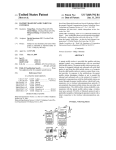
DIGITAL CAMERA WITH MEMORY
FORMAT INITIALIZATION
grabber” (a digital circuit board installed into PCs that
convert video images into PC compatible formats) of the
This is a continuation of US. patent application Ser. No.
09/253,831, ?led Feb. 19, 1999, now US. Pat. No. 6,233,
010 Which is a continuation of Ser. No. 08/712,493, ?led
Sep. 11, 1996, pending Which is a continuation of Ser. No.
08/098,787, ?led Jul. 29, 1993, now US. Pat. No. 5,576,
757, Which is a continuation of Ser. No. 07/878,603, ?led
May 5, 1992, noW abandoned, Which is a continuation of
Ser. No. 07/615,848, ?led Nov. 20, 1990, now US. Pat. No.
Micro, RasterOps, and others or convert the image to a
type sold commercially by Aapps Corporation, Orange
hard-copy print (a photograph) and utiliZe an electronic
“scanner”, a piece of equipment that connects to a PC, Which
converts an image into a digital format. The later technique
is employed extensively Within the desktop publishing
industry.
It is the object of this invention to provide an improved
5,138,459.
electronic still camera With operator selectable picture com
pression in one of a plurality of operator selectable digital
BACKGROUND OF THE INVENTION
1. Field of the Invention
This invention generally relates to an electronic still video
camera and in particular to an improved electronic still
15
camera Which converts a still picture of an object or scene
programs on PCs.
Personal Computer (PC) compatible format retaining the
images’ color information, and stored on a PC compatible
memory diskette. For example, the diskette can be a three 25
and a half (31/2) inch digital diskette. The digital diskette is
removeable from the electronic camera for direct insertion
30
35
a conventional prior art electronic still camera system, in
Which a CCD image sensor element 1a converts a still image
signal processing subsystem 3a Where the signal is con
more ef?cient electronic still camera that can take a still
40
standard Phase Alternating Line-PAL) and logged in analog
analog video ?oppy disk, Electrically Erasable Program
mable Read Only Memory (EEPROM), analog audio
(IR), and Ultra Violet (UV) Which can be directly or
remotely controlled by analog, digital, or radio frequency
(RF) control signals.
A further object of this invention is to provide a program
cassette, bubble memory, or other storage device 5a. PoWer
mable video picture translator device for ef?ciently convert
is supplied by a rechargeable/removeable battery system 4a.
ing electronic still images in analog composite video format
50
tronic image signals and transferred to a memory storage
device is disclosed in the following US. Pat. Nos. 4,131,
into digital data format readable by a PC. This translator
device also provides additional video inputs and outputs for
capturing video images, monitoring video images on moni
919; 4,456,931; 4,758,883; 4,803,554; and 4,837,628.
tors and displays, and can transmit either compressed or
Conventional prior art electronic still cameras, for
unprocessed digital image data through a variety of output
55
I/O channels in various formats such as serial, parallel, etc.
Also, this invention can incorporate sound/voice With
images thru additional interface circuitry and audio digitiZ
vision System Committee (NTSC) or similar on magnetic or
electronic storage media for either permanent or temporary
storage to facilitate vieWing on a television or video monitor.
picture With operator selectable high, medium, or loW reso
lution in either color or black and White by electronic shutter
and exposure control by utiliZing a variety of electro-optical
sensors including Charge Coupled Devices (CCD), Infrared
format onto a mass memory storage device such-as an 45
example of the types disclosed in the aforementioned
references, produce an electronic signal corresponding to a
desired image in analog format such as the National Tele
series of images automatically as Well as singularly. Also,
this camera provides multiple outputs in both video format
for monitor and display of images and digital formats to
facilitate data transmission, additional processing, or storage
to a variety of storage media.
It is still another object of this invention is to provide a
verted to National Television System Committee (NTSC) or
other composite video formats (such as the European video
An electronic camera that converts an image into elec
With each image frame.
electronic still camera device that can rapidly capture a
applications.
of an object into an analog color video signal When the
shutter control circuitry 2a is activated. The output color
video signal of the image sensor element is then routed to the
storage of a large number of images With the signal ?ag
indicating the degree of compression selected by the opera
An additional object of this invention to provide an
processing, desk top publishing, data base, and multi-media
2. Description of the Prior Art
FIG. 1 is a schematic block diagram shoWing structure of
It is another object of this invention is to provide an
improved electronic still camera that, under user selection,
can record and store still images selectively compressed in
a directly insertable digital memory storage device into a PC
in either color or black and White formats thus facilitating
tor as Well as the color/black and White mode selection being
stored as digital values on the digital memory storage device
into a PC Which contains the previously loaded correspond
a format compatible for immediate use With Word
data formats recordable on a standard removeable magnetic
diskette common to personal computers.
It is a further object of this invention to provide an
improved electronic still camera that provides digital image
?les for immediate and direct incorporation into popular
Word processing, desktop publishing, and other softWare
into an operator selectable compressed digital signal format
for storage utiliZing a compression/decompression
algorithm, such as the Joint Photographic Experts Group
(JPEG) algorithm standard for example, formatted into
ing decompression algorithm Whereby the digital image is in
SUMMARY OF THE INVENTION
10
ers.
60
With the current state of the art, it is expensive and time
consuming to convert the analog image equivalent to a
digital format for direct utiliZation With PC softWare appli
Finally, it is the object of this invention to provide an
electronic still camera that is ef?cient in design and permits
extended periods of portable operation and Which provides
the user With operational status through the use of continu
ous internal self-test softWare routines and operator displays.
cations. Currently, to convert an image captured on an
electronic still camera to a PC compatible format one must 65
convert the signal back to either a composite-NTSC or ROB
video signal and use a conversion device such as a “frame
BRIEF DESCRIPTION OF THE DRAWINGS
FIG. 1 is a schematic block diagram of a conventional
prior art electronic still camera.
US 6,496,222 B1
3
4
FIG. 2 is a schematic block diagram of the of the overall
structure of an electronic still camera embodying the present
invention.
initiated by the operator via control panel 2. When taking a
picture, focusing and shutter speed are controlled by a lens
system and shutter speed selection mechanism under control
of the digital control unit 9. The camera, like other still video
FIG. 2A is an illustration shoWing one embodiment of an
cameras, employs an electronic shutter system that controls
a charge storage time in a CCD array onto Which an image
of an object is focused through the lens system.
audio data ?le, data format ?ag, compression level, and
color/black and White mode selection values stored on a
digital memory diskette storage device.
When the “shoot” control 6 is half depressed (see FIG. 6),
a poWer supply voltage is supplied from the rechargeable
FIG. 3 is a ?oWchart shoWing the poWer-up and continu
ous self-test sequence in accordance With one aspect of the
present invention.
10
9, control panel 2, and the disk drive assembly 5. The
exposure control circuitry not shoWn generates appropriate
FIG. 4 is an example of a 1/2“ CCD array utiliZable in
accordance With one aspect of the present invention.
horiZontal and vertical transfer pulses as Well as ?eld shift
pulses under control of the reference clock timing and
FIG. 5A is a schematic block diagram shoWing the image
signal to digital signal conversion logic in accordance With
15
one aspect of the present invention.
FIG. 5B is a logic and timing diagram for the image signal
to digital signal conversion logic in accordance With one
aspect of the present invention.
FIG. 6 is an example of the control panel logic in
accordance With one aspect of the present invention.
FIG. 6A is an example of one embodiment of sWitch logic
of the control panel sWitches and controls utiliZable in
accordance With one aspect of the present invention.
FIG. 6B is an example of the PICT image ?le format
25
based upon the published standard provided by Apple
Computer, Inc.
design may be of any type Well knoWn in the art for example
those cited in US. Pat Nos. 4,131,919 and 4,456,931 and
any similar designs Well knoWn in the prior art.
An-alternate embodiment of the present invention that
provides remote operation of the camera is shoWn in FIG.
6C. When remote “Shoot” control 30 is activated by any
means for example manually, or by radiant, or electronic
energy, a control signal is generated and routed through the
external jack 31, located on the external camera body. The
external control 30 is electrically connected to the external
familiar to those skilled in the art Upon receipt of the
externally generated “shoot” command, the relay sWitch 32
tion embodying remote operation.
is activated and provides internal sWitch closure. This clo
sure of sWitch 32 then initiates the process previously
described and provides the half V+ voltage previously
described. The full V+ is provided via the ?xed delay 33, the
value chosen to alloW the diskette drive assembly 5 (FIG. 2)
35
and associated control circuitry to initialiZe prior to receiv
ing image data.
FIG. 9 is a block diagram of a video format translator
device in accordance With one aspect of the present inven
tion.
FIG. 10 is a block diagram illustrating the operation of a
translator device in accordance With one aspect of the
When the “shoot” control is fully depressed in either
embodiment, the shutter controller 15 (FIG. 6) generates a
shutter pulse that generates control signals for the A/D
converters 8 alloWing the image/picture data signal in the
sample and hold circuitry of the pixel multiplexer 7 to be
present invention.
FIG. 11 is an alternative embodiment of the video format
translator in accordance With another aspect of the present
invention shoWing additional video inputs and data outputs.
control signals provided by the digital control unit 9 type for
driving the CCD device and pre-processing circuitry. This
jack 31 by a tWisted-pair conductive cable assembly that is
FIG. 6C is an alternate embodiment of the current inven
FIG. 7 is a simpli?ed block diagram of the digital control
unit in accordance With one aspect of the present invention.
FIG. 8 is a ?owchart shoWing the steps of the image
compression algorithm in accordance With one aspect of the
present invention.
batteries 4 to the electronic circuits and digital control unit
45
converted into a digital signal. Control and address instruc
tions of the type Well knoWn in the art are generated from the
digital control unit 9 to facilitate the storage of the digital
image data Within the pixel buffer 10 and frame buffer 11.
Upon completion of image conversion, the contents of the
FIG. 12 is an alternate embodiment of the invention
shoWing an optional diskette format utility ?oWchart.
frame buffer are transferred to the compression processor 12
FIG. 13 is an alternate embodiment of a frame buffer
Which for example may be of the many versions currently
utiliZable in accordance With another aspect of the present
invention shoWing a frame buffer stack permitting multiple
shot mode.
four chip Application Speci?c Integrated Circuit (ASIC) set.
offered commercially such as C-Cube’s (San Jose, Calif.)
In the compression processor 12, the Joint Photographic
Experts Group (JPEG), a part of the International Standards
OrganiZation (ISO) Which is a subset of the International
FIG. 14A is a block diagram of an embodiment of the
format select logic in accordance With one aspect of the
present invention.
FIG. 14B is a How diagram illustrating the steps of the
55
Telegraph and Telephone Committee (CCITT), image com
pression algorithm fully described in Report #JTC1/SC2/
WG8 dated 1985 is performed under control of the digital
control unit 9 to compress the siZe of the image. Avariable
selectable compression ratio of up to 50:1 is performed on
the digital image frame. Other compression ratios are opera
tor selectable via the control panel 2 sWitches 14A and 14B
format selection logic operations.
DESCRIPTION OF THE PREFERRED
EMBODIMENT
(FIG. 6). The compressed digital frame is then formatted
FIG. 2 is a schematic block diagram of the preferred
embodiment of an electronic still camera in accordance With
into either an IBM PC/Clone (such as GIFF) or Apple
the principals of the invention. Referring to FIG. 2, an image
optical pick-up element 1, Which for example could be a
Macintosh (such as PICT II) image ?le format depending on
the setting selected by the operator for a user sWitch 17 (FIG.
6) position on the control panel 2. After formatting, the ?le
Charge Coupled Device (CCD) (or an Infrared (IR) or
65
Ultraviolet (UV) sensor), converts a still image of an object
is Written into a temporary memory buffer Within the disk
into an electric signal When a picture “shoot” command is
input output (I/O) interface circuit 13 Which, under the
US 6,496,222 B1
5
6
command of the digital control unit 9, controls the high
embodiment Would be appropriately marked or tagged With
density (1.4 Mbyte storage capacity) disk drive unit 5.
the corresponding digitiZed audio ?le 56 (FIG. 2A). Upon
Following ?le transfer to the diskette e.g., the frame counter
playback on a sound con?gured PC, both the image and the
corresponding audio Would then be vieWed and heard simul
display 22 on the control panel 2 is updated by appropriate
control signals and the camera is ready to undergo the same
procedure for the neXt image. PoWer to the electronic
circuits and disk drive system is terminated folloWing
release of the “shoot” control sWitch 6.
In accordance With the preferred embodiment of this
invention, it is permissible for the user to select various
taneously.
It should be noted that a major advantage a camera in
accordance With the present invention has over conventional
still video cameras is that a camera according to this
invention is capable of storing multiple digital images in
10
resolution quality image recording levels With the higher
semiconductor memory temporarily at a rapid rate While,
simultaneously, the image compression processor 12, ?le
levels being at the eXpense of memory diskette storage
formatter softWare algorithm, and disk I/O interface 13 that
capacity. The position of sWitches 14A and 14B for eXample
stores formatted ?les continue to function in concert
could represent a unique digital mark or Word that denotes
the respective sWitch position and is sensed during initial
15
poWer application and periodically during operation. FIG.
together at a sloWer rate. This efficient design coupled With
VLSI loW poWer, high speed semiconductor memory
devices (10 & 11 FIG. 5A and 24 FIG. 7) alloWs this
operational capability.
6A illustrates typical logic AND gate circuits 60a and 60b
utiliZable in conjunction With sWitches 14A and 14B or
Like most other still video and conventional ?lm cameras,
sWitch 17 to generate appropriate signals to designate
When the “shoot” control 6 (FIG. 6) is fully depressed, a
control signal is generated from the digital control unit 9 that
respective sWitch positions and generate appropriate control
signals from. The sWitch positioned in the High position for
generates a trigger signal on the control panel 2 to cause a
high resolution alloWs only four to ?ve images to be stored,
While Med, sWitch position for medium resolution alloWs
approximately tWenty ?ve images to be stored, and LoW for
?ash unit 16 (FIG. 6) to irradiate a ?ash of light onto the
loW resolution alloWs up to ?fty images to be stored on a
25 diskette such as a standard three and a half inch or similar
single diskette. Also, by selecting black and White mode
storage medium. Various memory diskette siZes and formats
are suitable for the invention. HoWever, for the preferred
subject image.
During initial camera operation, the user ?rst inserts a
instead of color via sWitch 14B, the operator may select
additional storage capacity since storage is increased by a
factor greater than three (one element per piXel versus three
for color). Various image resolution combinations are per
embodiment either a double-density (800 Kbytes of storage)
or a high-density (1.4 Mbytes of storage) diskette in a three
and a half inch format Which are readily available from
various commercial sources such as Sony, MaXell, and
Verbatim. The user must then select the desired PC format
missible because the operator can select a different resolu
tion and mode setting for each image prior to image signal
capture. This is accomplished by marking or “tagging” each
(IBM PC/Clone or Apple Macintosh, etc.) via sWitch 17
image frame data information signal With the resolution and
mode of each image as it is Written onto the memory diskette
in any suitable manner, for eXample as shoWn in FIG. 2A.
With reference to FIG. 2A, diskette 50 has tracks 51a,
(FIG. 6) on the control panel 2. As shoWn in FIG. 3.; after
35
circuitry, battery, disk drive unit, and control panel. Should
any failures be detected, an appropriate error indicator is
illuminated on the control panel. During the poWer-one
sequence (see FIG. 3 and FIG. 12), the inserted diskette 50
52b, . . . 5211. With reference to track 52b there is shoWn a
representative portion of segment 53 depicting a typical
image ?le information format having digital bit 54 depicting
color mode, and digital bits 55 representing compression
resolution level markings or tags. With reference to color
mode tag 54 it can be seen that if sWitch 14B is in the color
position tag 54 is recorded as a logical “one” or true
conversely if bit 54 is recorded as a logical “Zero” it
turning on the poWer sWitch or inserting a diskette 50, the
digital control unit 9 performs a self test of all internal
is automatically checked for formatting consistencies in
45
accordance With the format selected by the format sWitch 17
on the control panel 2 (IBM/Apple/etc.) and for available
storage space by checking the boot block on the diskette, a
technique that Will be familiar to those skilled in the art.
corresponds to the black and White position of sWitch 14B.
Should any inconsistencies be detected, an error indicator is
Similarly as shoWn sWitch 14A Would record in memory
position 55 a binary “Zero” for loW resolution, a binary
“one” for medium resolution and a binary “tWo” for high
illuminated on the control panel (ie, disk full, unformatted,
etc.). The operator frame counter display 22 (FIG. 6) is then
updated to shoW the maXimum number of pictures available
based upon indicated operator selections (color/black and
resolution selections by the operator. By incorporating this
“tagging” approach, it is possible for the decompression
White), diskette type (double versus high density), and
capacity (partially full versus empty diskette). During
algorithm, loaded into any PC prior to use or Written onto the
memory storage diskette along With the image data, to
automatically determine the appropriate level of compres
sion associated With image ?le and eXecute decompression
operation, the operator can selectively erase a frame and
record over it if desired by selecting the erase mode of
55
operation from the control panel and toggling the forWard/
ef?ciently.
reverse control.
Still another alternate embodiment in accordance With this
invention incorporates an acoustic digitiZer circuit Which
The optics for the preferred embodiment of the invention
is a commercially available one-half inch (l/z“) color CCD
device having a piXel grid array of 780x488 as pictorially
depicted in FIG. 4. This results in 380,640 piXel elements
Which results in a commercially acceptable quality resolu
tion image as Will be understood by those skilled in the art.
digitiZes sound. There are several digitiZers commercially
available such as the Apple Computer Inc. Musical Instru
ment Data Interface (MDI) adaptor. The output of this
digitiZer may be selectively connected to the CPU 20 (FIG.
7) via an additional I/O interface similar to the auXiliary I/O
interface 80. The sound or audio associated With each image
can be recorded, digitiZed, and stored on the diskette device
In a color imaging device (CCD array) photoelectric
elements, such as photodiodes, are arranged in a tWo dimen
on available tracks in an identical manner previously
sional array With optical ?lters for R (red), G (green), and B
(blue). Various arrangements of optical ?lters are Well
described (FIG. 2A). An image ?le in accordance With this
knoWn and the arrangement of optical ?lters is not limited to
65
US 6,496,222 B1
7
8
a particular one With this invention. During operation each
pixel stores a charge corresponding to the amount of incident
light. The RGB components of each pixel’s charge is
iaturiZed packaging techniques such as surface mount
devices (SMD) and ASIC technology make it feasible to
incorporate these devices in a parallel design in order to
sequentially read out via a horiZontal/vertical addressing
realiZe a substantial increase in conversion speed With no
scheme that Will be familiar to those skilled in the art.
appreciable increase in poWer consumption. Therefore, this
As shoWn in FIG. 5A; each charge, When addressed, is
ampli?ed and processed in a sample and hold (S/H) circuit
18. The analog voltage in each S/H circuit is digitiZed by an
associated analog to digital
converter 8. The digital
design approach provides signi?cant conversion throughput
values are routed and collected in the pixel buffer 10.
10
FolloWing completion of discrete pixel element conversion
and subsequent formatting in the pixel buffer Which is under
Control Processor Unit (CPU) 20 softWare control, the
output of the full pixel buffer is routed to the frame buffer 11
by digital control unit 9. This process continues until a
complete frame is collected Within the frame buffer. The
present invention (FIG 5A) requires approximately 380,
640x150 nsec. or 38 milliseconds (msec.). Additional time
15
general digital logic and timing and control signals for this
circuitry is shoWn in FIG. 5B. The timing is provided by a
master clock that is an integral part of the CPU micropro
cessor. For example, the MOTOROLA 68040 microproces
sor has a clock speed of approximately 40 MegahertZ (MZ
Which results in a clock period of 25 nanoseconds (nsec.).
This clock pulse is used by the function and address decoder
19 (FIG. 6) to generate the address and control signals
shoWn in FIG. 5B as Would be understood by those skilled
in the art. The circuit of the present invention may be
designed by one skilled in the art to function With a variety
of microprocessor architectures and is not limited to any one
in particular. One can see from the timing chart that the S/H
circuit is alloWed (via the SE command) to charge to a
signal latency. Thus, total conversion time for a complete
image frame prior to compression processing and logging to
second period. By adding additional RAM 11A (FIG. 13) or
20
other forms of commercially available random access
memory to the frame buffer 11, image frames could be
“pushed” onto a semiconductor memory stack for temporary
storage alloWing the compression processor and data inter
25
face circuitry to perform their respective functions at a
sloWer rate. As shoWn in FIG. 13, each unprocessed image
frame Would be recorded or “pulled” from the stack on a
“First-In, First-Out” (FIFO) manner until all images in the
stack queue Were processed and Written to the storage
30
diskette via the disk I/O circuitry 13.
As shoWn in FIG. 6, control panel settings are monitored
by the CPU 20, a microprocessor, thus alloWing the appro
35
properly. The microprocessor 20 may be of the type 68040
manufactured by MOTOROLA, Intel’s 80386 series, or
equivalent microprocessors Which speci?cations are com
mercially available and are incorporated herein by reference.
The microprocessor utiliZation of this invention, Which is in
priate timing, control, and signal processing to be effected
upon the pixel element (via the PS command). After a ?xed
time period, the A/D converters are enabled(via the CE
command) to begin conversion of the analog voltage value
completion signal (CC) is generated by the A/D and routed
back to the S/H circuit (via the SC command Which is
generated by the function and address controller 19) to
discharge the stored analog voltage in anticipation of the
next pixel element conversion process. Next, the output of
the A/D converter 8 is clocked into the pixel buffer 10 (via
the PB command). When the pixel buffer 10 is full, the
(approximately 5 msec.) is required for timing and control
the memory storage diskette 50 is less than ?fty msec. This
alloWs for approximately 20 images to be captured in a one
voltage level indicative of the analog voltage impinging
on the S/H. Upon completion of conversion a conversion
increases over previous designs.
The extremely high conversion speed in accordance With
another concept of the present invention makes multiple
high-speed camera operation possible in an alternate
embodiment. For example, total conversion time required
for the aforementioned CCD array utiliZing the circuit of the
the digital control unit 9, transmits commands and status to
speci?c controls, functions, and displays in the control panel
40
as Well as receiving both circuit status/control data and
operator commands through polling the operator sWitch
settings 14A, 14B, and 17 via the bidirectional function and
output is clocked out to the frame buffer 11 (via the FB
address decoder 19. This approach alloWs the user to knoW
command) and the pixel multiplexer address circuitry selects
immediately hoW much storage capacity remains in the
the next pixel for conversion. Reset signals (RST) are sent
45
to all circuit elements to alloW these devices to reset prior to
displays 21, 22, and 23 and ongoing softWare self-tests
running in the background as depicted in FIG. 3. An example
of this Would be a loW battery situation. First, the digital
receiving the next analog value.
Another novel concept of the present invention as illus
trated in FIGS. 5A and 5B utiliZes a technique of paralleling
the S/H and A/D devices for each pixel element thus
image storage diskette 50 as Well as the camera’s overall
operational and functional status through the use of status
50
control unit 9 Would detect a failure in the self-test mode.
accelerating the image signal analog-to-digital conversion
Next, the self-test light emitting diode 21 (FIG. 6) Would be
process. This is accomplished by eliminating the serial S/H
and A/D path typical of prior art still video camera designs.
In addition, high-speed, loW-poWer devices available from
Sony, Burr-BroWn, Datel, Analog Devices, and others facili
illuminated and an appropriate error display Would be illu
minated in the status display 22 thus providing the user With
an exact indication of the error. Another example illustrating
55
tate the increased conversion throughput of the S/H and AID
circuits With pixel conversion times of less than 150 nano
seconds (nsec.). For example, Sony’s video A/D converter
Device part number CXA 1016P/K performs up to 50
million samples per second or 20 nsec. per conversion. This
device, or similar, may be used in the preferred embodiment
of the present invention. As explained previously, prior art
still video camera designs multiplex each signal component
into a common/singular A/D path to reduce the number of
components and poWer consumption. HoWever, in accor
dance With another aspect of the present invention compo
nents such as CMOS and ECL devices coupled With min
60
the operation of this embedded microprocessor type of
control approach is the format sWitch 17 (FIG. 6). The
position of the format sWitch 17 is sensed upon poWer
application. FolloWing diskette insertion, the boot block on
the diskette is compared With the format sWitch 17 setting
(IBM/clone or Apple) and if the format does not match or if
the disk 50 is unformatted, the disk format status light
emitting diode 23 Would be illuminated and an appropriate
error display Would be illuminated in the status display 22
thus prompting the user to take appropriate corrective mea
65 sures.
An alternate embodiment of the present invention
involves adding an auxiliary I/O interface circuit or port to
US 6,496,222 B1
9
10
the digital control unit 9. As shown if FIG. 7, the auxiliary
feasible for this invention include the Fast Fourier Trans
I/O port 80 connects in a manner similar to the Disk I/O
form (FFT), Discrete Cosine Transform (DCT), and Discrete
Sine Transform (DST). The DCT Was adopted by the JPEG
as the preferred algorithm due to computational simplicity
interface 13. This additional I/O channel provides for exter
nal control and monitor of all timing and control signals
internal to the camera. In addition, it alloWs for the image
data to be routed past or around the compression processor
and performance.
It should be noted that the Joint Photographic Experts
Group (JPEG) (composed of experts from many companies
including IBM, AT&T, Digital Equipment Corp, and
out to any additional internal or external device such as an
optical disk storage device, digital analyZer, or other data
processors that might be desired.
FIG. 7 shoWs the digital control unit 9. The microproces
10
sor 20 architecture here is typical to one familiar With the art.
The frame buffet 11 (FIG. 5A) receives and stores the
outputs of the pixel buffer 10 until a complete frame of
image data is received. Then, the CPU 20, under softWare
control, issues a control signal to the optics logic in the
standard provides image compression effectively up to 75
15
shutter and control circuitry 15 (FIG. 6) thus resetting those
functions for future image recording. The full frame buffer
11, upon command from the CPU 20, transfers it’s data into
the compression processor 12 (FIG. 2) Which performs
thousands of levels of parallel pipeline processing on the
image data. The compressed image frame is then Written out
to the mass memory RAM (Random Access Memory) 24
Where it is temporarily stored until transferred to the disk
drive assembly 5 via the disk I/O interface circuitry 13.
Referring to FIG. 8, a ?oWchart shoWs the steps involved
20
25
times or greater depending on the visual ?delity desired. The
J PEG standard is Widely used in industry as an alternative to
proprietary algorithms such as Intel’s oWn proprietary stan
dard called DVI Which Was initially developed by RCA
before being sold to INTEL, the integrated Circuit manu
facturer. INTEL offers it’s oWn ?rmWare compression pro
cessor incorporating their DVI standard delivering compres
sion ratios in excessive of 100:1. HoWever, a neW
international standard called MPEG is due to be announced
in the 1991 time frame from the JPEG and should offer
compression ratios of 275:1 and greater. In the preferred
embodiment of the present invention, the JPEG standard is
the preferred algorithm chosen With the incorporation of the
the MPEG standard or other similar standard in the future
in the image compression process performed by the image
compression processor 12 (FIG. 2) in accordance With the
preferred embodiment of the present invention. The output
of the frame buffer 11 is transferred into the input of the
image compression processor 12 under the control of the
digital control unit 9. As previously described, the setting of
sWitch 14A (FIG. 6) is read by the CPU 20 (FIG. 7) to
INTEL) compression/decompression standard Was devel
oped in 1985 in response to the lack of interoperability
betWeen image and processing equipment due to numerous
proprietary standards held by each manufacturer. The JPEG
When available commercially. An alternate embodiment of
the present invention Would be the incorporation of various
proprietary compression algorithm standards such as DVI.
30
The compression/decompression algorithm ?rmWare
implementation of the JPEG algorithm is available commer
cially from various sources including C-Cube, Electronics
determine the image resolution quality desired. Depending
for Imaging, Storm Technology, Burr-BroWn, Spectral Inno
on the operator selected setting of sWitch 14A, the unique
vations Inc., INTEL, and others. The implementation of this
algorithm for the present invention may incorporate the
integrated circuit set commercially available from C-Cube.
Their four chip ASIC JPEG algorithm implementation is
performed in three basic steps: ?rst, the image is divided into
8-by-8 pixel squares and applies a discrete cosine transform
(DCT) to each square resulting in 64 frequency values;
second, these frequencies are put through a quantiZation
digital Word generated by the AND gate 60a—b (FIG. 6A)
35
Which is activated by the selected position of sWitch 14A is
routed to image compression processor 12 via CPU 20 (FIG.
7) Which selects for example a predetermined digital
memory location containing the appropriate corresponding
compression ratio parameters under program control. The
40
compression processor uses this command value for
example to establish the siZe of the covariance matrix and a
threshold for acceptance for the variances produced by the
Discrete Cosine Transformation (DCT) transform coeffi
cients. Next, the digital image signals are converted from the
RGB format previously discussed in connection With FIGS.
2, 5, and 6 into luminance and chrominance signals. The
luminance and chrominance signals subsequently undergo a
DCT. The cosine transformed signals are then quantized and
are then processed for Huffman coding. The Huffman coded
algorithm to eliminate unimportant frequencies; third, the
remaining values are run through a Huffman coding scheme
45
to encode the most frequently occurring values using the
feWest bits. A compatible softWare implementation of the
JPEG algorithm is available commercially from Aladdin
Systems, Radius Inc., Kodak, and others.
Those skilled in the art Will be familiar With the process
and the commercially available softWare and ?rmWare
50
chipsets that are currently available on the market. The
image signals are then formatted into a form that facilitates
present invention incorporates both available ?rmWare
format processing into various PC compatible formats
(GIFF, PICT2, etc.). For a more complete understanding of
the image compression process reference may be made to
I.E.E.E. Catalog No. EH0231-1, Library of Congress No.
85-60384 published by the I.E.E.E. Society dated 1985 and
chipsets in the camera and softWare for use in the PC for
decompression. The decompression algorithm can be Writ
55
incorporated herein by reference.
image ?le selected by the user is automatically decom
Of the tWo traditional classes of image compression
pressed transparent to the user. The algorithm can be Written
techniques, spatial coding and transform coding, transform
coding techniques lend themselves Well for this application
due to computational simplicity. Transform coding tech
niques that provide good visual ?delity include: Karhunen
Loeve transform (KLT), Fourier, cosine, sine, and Had
amard. The KLT algorithm offers the best visual ?delity but
suffers from serious computational complications due to
ten onto the camera’s diskette 50 prior to any image data
recording. This alloWs the PC user to take the diskette 50 to
a PC and directly incorporate the image data because the
onto an unused track 52 or sector combination on the
60
diskette as shoWn on FIG. 2A. Alternatively, the decom
pression algorithm can be loaded onto a PC before inserting
a diskette 50 containing compressed image data. In the latter
embodiment the resolution and mode values 54 and 55 (FIG.
2A.) for each representative image Would be read from
65
diskette 50 in order to appropriately control the selection and
extremely large matrix siZe. Several alternate algorithms
activation of the appropriate corresponding decompression
that offer reasonable visual ?delity that are computationally
algorithm.