1
Reference
Guide
2002
Real World Signal Processing
Printed in U.S.A., November 2002
SDS
SPRU161D
2002
Reference
Guide
TMS320F/C240 DSP Controllers
Reference Guide
Peripheral Library and Specific Devices
Literature Number: SPRU161D
November 2002
Printed on Recycled Paper
IMPORTANT NOTICE
Texas Instruments Incorporated and its subsidiaries (TI) reserve the right to make corrections,
modifications, enhancements, improvements, and other changes to its products and services at
any time and to discontinue any product or service without notice. Customers should obtain the
latest relevant information before placing orders and should verify that such information is current
and complete. All products are sold subject to TI’s terms and conditions of sale supplied at the
time of order acknowledgment.
TI warrants performance of its hardware products to the specifications applicable at the time of
sale in accordance with TI’s standard warranty. Testing and other quality control techniques are
used to the extent TI deems necessary to support this warranty. Except where mandated by
government requirements, testing of all parameters of each product is not necessarily performed.
TI assumes no liability for applications assistance or customer product design. Customers are
responsible for their products and applications using TI components. To minimize the risks
associated with customer products and applications, customers should provide adequate design
and operating safeguards.
TI does not warrant or represent that any license, either express or implied, is granted under any
TI patent right, copyright, mask work right, or other TI intellectual property right relating to any
combination, machine, or process in which TI products or services are used. Information
published by TI regarding third party products or services does not constitute a license from TI
to use such products or services or a warranty or endorsement thereof. Use of such information
may require a license from a third party under the patents or other intellectual property of that third
party, or a license from TI under the patents or other intellectual property of TI.
Reproduction of information in TI data books or data sheets is permissible only if reproduction
is without alteration and is accompanied by all associated warranties, conditions, limitations, and
notices. Reproduction of this information with alteration is an unfair and deceptive business
practice. TI is not responsible or liable for such altered documentation.
Resale of TI products or services with statements different from or beyond the parameters stated
by TI for that product or service voids all express and any implied warranties for the associated
TI product or service and is an unfair and deceptive business practice. TI is not responsible or
liable for any such statements.
Mailing Address:
Texas Instruments
Post Office Box 655303
Dallas, Texas 75265
Copyright 2002, Texas Instruments Incorporated
Preface
Read This First
About This Manual
The purpose of this user’s guide is to assist you, the hardware or software engineer, in developing applications using the TMS320C240/F240 digital signal
processors (DSPs).
Throughout this book, the TMS320C240 and the TMS320F240 (with on-chip
flash EEPROM) are generally referred to as the ’240.
For more information about the ’240 CPU and instruction set, see
TMS320F/C24x DSP Controllers CPU and Instruction Set Reference Guide
(literature number SPRU160).
For known exceptions to the functional and emulation specifications for the
’240, refer to TMS320F240 DSP Controller Silicon Errata (Silicon
Revisions 1.1, 2.0, 3.1, 3.2, and 3.4) (literature number SPRS066).
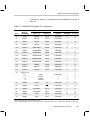
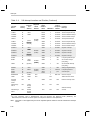
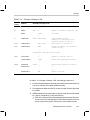
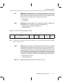
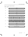
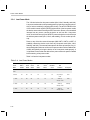
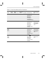
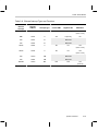
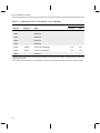
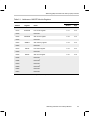
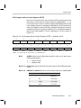
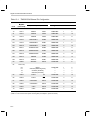
How to Use This Manual
The following table summarizes the ’240 information contained in this manual
(refer to the Table of Contents for a complete listing):
If you are looking for
information about
Turn to
Digital I/O ports
Chapter 12, Digital I/O Ports
Dual 10-bit A/D converter
Chapter 7, Dual 10-Bit Analog to Digital
Converter (ADC) Module
Event manager
Chapter 6, Event Manager Module
External memory interface
Chapter 11, External Memory Interface
PLL clock module
Chapter 4, PLL Clock Module
Serial communications interface
Chapter 8, Serial Communications
Interface (SCI) Module
Serial peripheral interface
Chapter 9, Serial Peripheral Interface
(SPI) Module
Watchdog and real-time interrupt
module
Chapter 5, Watchdog (WD) and
Real-Time Interrupt (RTI) Module
iii
Contents
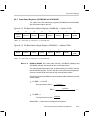
Notational Conventions / Information About Cautions
Notational Conventions
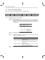
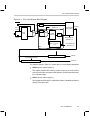
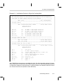
This document uses the following conventions:
- Program listings and program examples are shown in a special type-
face.
Here is a segment of a program listing:
OUTPUT LDP
BLDD
RET
#6
#300, 20h
;select data page 6
;move data at address 300h to 320h
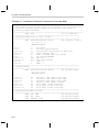
- Hexadecimal numbers are represented with a lowercase letter h following
the number. For example, 7400h or 743Fh.
- In syntax descriptions, the instruction is in a bold typeface and
parameters are in an italic typeface. Portions of a syntax in bold must be
entered as shown; portions of a syntax in italics describe the type of
information that you specify. Here is an example of an instruction syntax:
BLDD source, destination
BLDD is the instruction and has two parameters, source and destination.
When you use BLDD, the first parameter must be an actual data memory
source address and the second parameter must be a destination address.
A comma and a space (optional) must separate the two addresses.
- Square brackets, [ ], identify an optional parameter. If you use an optional
parameter, specify the information within the brackets; do not type the
brackets themselves. When you specify more than one optional parameter from a list, you separate them with a comma and a space. Here is a
sample syntax:
BLDD source, destination [, ARn]
BLDD is the instruction. The two required operands are source and
destination, and the optional operand is ARn. AR is bold and n is italic; if
you choose to use ARn, you must type the letters A and R and then supply
a chosen value for n (in this case, a value from 0 to 7). Here is an example:
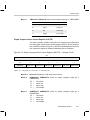
Information About Cautions
This book contains cautions.
This is an example of a caution statement.
A caution statement describes a situation that could potentially
damage your software or equipment.
iv
Related Documentation from Texas Instruments
Related Documentation from Texas Instruments
The following books describe the ’F/C240 and related support tools. To obtain
a copy of any of these TI documents, call the Texas Instruments Literature
Response Center at (800) 477–8924. When ordering, please identify the book
by its title and literature number. Many of these documents are located on the
internet at http://www.ti.com.
TMS320F/C24x DSP Controllers CPU and Instruction Set Reference
Guide (literature number SPRU160) describes the TMS320F/C24x
16-bit fixed-point digital signal processor controller. Covered are its
architecture, internal register structure, data and program addressing,
and instruction set. Also includes instruction set comparisons and design
considerations for using the XDS510 emulator.
TMS320F243/F241/C242 DSP Controllers System and Peripherals
Reference Guide (literature number SPRU276) describes the
architecture, system hardware, peripherals, and general operation of the
TMS320F243, ’F241, and ’C242 digital signal processor (DSP)
controllers.
TMS320F240 DSP Controller (literature number SPRS042) data sheet
contains the electrical and timing specifications for the TMS320F240
device, as well as signal descriptions and pinouts for all of the available
packages.
TMS320F20x/F24x DSP Embedded Flash Memory Technical Reference
(literature number SPRU282) describes the operation of the embedded
flash EEPROM module on the TMS320F20x/F24x digital signal
processor (DSP) and provides sample code that you can use to develop
your own software.
TMS320C1x/C2x/C2xx/C5x Code Generation Tools Getting Started
Guide (literature number SPRU121) describes how to install the
TMS320C1x, TMS320C2x, TMS320C2xx, and TMS320C5x assembly
language tools and the C compiler for the ’C1x, ’C2x, ’C2xx, and ’C5x devices. The installations for MS-DOS, OS/2, SunOS, and Solaris
systems are covered.
TMS320C1x/C2x/C2xx/C5x Assembly Language Tools User’s Guide (literature number SPRU018) describes the assembly language tools (assembler, linker, and other tools used to develop assembly language
code), assembler directives, macros, common object file format, and
symbolic debugging directives for the ’C1x, ’C2x, ’C2xx, and ’C5x generations of devices.
Read This First
v
Related Documentation from Texas Instruments
TMS320C2x/C2xx/C5x Optimizing C Compiler User’s Guide (literature
number SPRU024) describes the ’C2x/C2xx/C5x C compiler. This C
compiler accepts ANSI standard C source code and produces TMS320
assembly language source code for the ’C2x, ’C2xx, and ’C5x generations of devices.
XDS51x Emulator Installation Guide (literature number SPNU070)
describes the installation of the XDS510, XDS510PP, and
XDS510WS emulator controllers. The installation of the XDS511
emulator is also described.
XDS522/XDS522A Emulation System Installation Guide (literature number SPRU171) describes the installation of the emulation system.
Instructions include how to install the hardware and software for the
XDS522 and XDS522A.
XDS522A Emulation System User’s Guide (literature number SPRU169)
tells you how to use the XDS522A emulation system. This book describes the operation of the breakpoint, tracing, and timing functionality
in the XDS522A emulation system. This book also discusses BTT
software interface and includes a tutorial that uses step-by-step
instructions to demonstrate how to use the XDS522A emulation system.
XDS522A Emulation System Online Help (literature number SPRC002) is
an online help file that provides descriptions of the BTT software user interface, menus, and dialog boxes.
JTAG/MPSD Emulation Technical Reference (literature number SPDU079)
provides the design requirements of the XDS510 emulator controller,
discusses JTAG designs (based on the IEEE 1149.1 standard), and
modular port scan device (MPSD) designs.
vi
Related Technical Articles
Related Technical Articles
The following technical articles contain useful information regarding designs,
operations, and applications for signal-processing systems. These articles
supplement the material in this book.
“A Greener World Through DSP Controllers”, Panos Papamichalis, DSP &
Multimedia Technology, September 1994.
“A Single-Chip Multiprocessor DSP for Image Processing—TMS320C80”,
Dr. Ing. Dung Tu, Industrie Elektronik, Germany, March 1995.
“Application Guide with DSP Leading-Edge Technology”, Y. Nishikori,
M. Hattori, T. Fukuhara, R.Tanaka, M. Shimoda, I. Kudo, A.Yanagitani,
H. Miyaguchi, et al., Electronics Engineering, November 1995.
“Approaching the No-Power Barrier”, Jon Bradley and Gene Frantz, Electronic
Design, January 9, 1995.
“Beware of BAT: DSPs Add Brilliance to New Weapons Systems”, Panos
Papamichalis, DSP & Multimedia Technology, October 1994.
“Choose DSPs for PC Signal Processing”, Panos Papamichalis, DSP &
Multimedia Technology, January/February 1995.
“Developing Nations Take Shine to Wireless”, Russell MacDonald, Kara
Schmidt and Kim Higden, EE Times, October 2, 1995.
“Digital Signal Processing Solutions Target Vertical Application Markets”, Ron
Wages, ECN, September 1995.
“Digital Signal Processors Boost Drive Performance”, Tim Adcock, Data
Storage, September/October 1995.
“DSP and Speech Recognition, An Origin of the Species”, Panos
Papamichalis, DSP & Multimedia Technology, July 1994.
“DSP Design Takes Top-Down Approach”, Andy Fritsch and Kim Asal, DSP
Series Part III, EE Times, July 17, 1995.
“DSPs Advance Low-Cost ‘Green’ Control”, Gregg Bennett, DSP Series Part
II, EE Times, April 17, 1995.
“DSPs Do Best on Multimedia Applications”, Doug Rasor, Asian Computer
World, October 9–16, 1995.
“DSPs: Speech Recognition Technology Enablers”, Gene Frantz and Gregg
Bennett, I&CS, May 1995.
Read This First
vii
Related Technical Articles
“Easing JTAG Testing of Parallel-Processor Projects”, Tony Coomes, Andy
Fritsch, and Reid Tatge, Asian Electronics Engineer, Manila, Philippines,
November 1995.
“Fixed or Floating? A Pointed Question in DSPs”, Jim Larimer and Daniel
Chen, EDN, August 3, 1995.
“Function-Focused Chipsets: Up the DSP Integration Core”, Panos
Papamichalis, DSP & Multimedia Technology, March/April 1995.
“GSM: Standard, Strategien und Systemchips”, Edgar Auslander, Elektronik
Praxis, Germany, October 6, 1995.
“High Tech Copiers to Improve Images and Reduce Paperwork”, Karl Guttag,
Document Management, July/August 1995.
“Host-Enabled Multimedia: Brought to You by DSP Solutions”, Panos
Papamichalis, DSP & Multimedia Technology, September/October 1995.
“Integration Shrinks Digital Cellular Telephone Designs”, Fred Cohen and
Mike McMahan, Wireless System Design, November 1994.
“On-Chip Multiprocessing Melds DSPs”, Karl Guttag and Doug Deao, DSP
Series Part III, EE Times, July 18, 1994.
“Real-Time Control”, Gregg Bennett, Appliance Manufacturer, May 1995.
“Speech Recognition”, P.K. Rajasekaran and Mike McMahan, Wireless
Design & Development, May 1995.
“Telecom Future Driven by Reduced Milliwatts per DSP Function”, Panos
Papamichalis, DSP & Multimedia Technology, May/June 1995.
“The Digital Signal Processor Development Environment”, Greg Peake,
Embedded System Engineering, United Kingdom, February 1995.
“The Growing Spectrum of Custom DSPs”, Gene Frantz and Kun Lin, DSP
Series Part II, EE Times, April 18, 1994.
“The Wide World of DSPs, ” Jim Larimer, Design News, June 27, 1994.
“Third-Party Support Drives DSP Development for Uninitiated and Experts
Alike”, Panos Papamichalis, DSP & Multimedia Technology, December
1994/January 1995.
“Toward an Era of Economical DSPs”, John Cooper, DSP Series Part I, EE
Times, Jan. 23, 1995.
viii
Trademarks
Trademarks
320 Hotline On-line, XDS510, XDS510PP, XDS510WS, XDS511, XDS522,
XDS522A, and Real World Signal Processing are trademarks of Texas
Instruments.
HP-UX is a trademark of Hewlett-Packard Company.
MS-DOS and Windows are registered trademarks of Microsoft Corporation.
OS/2, PC, and PC-DOS are trademarks of International Business Machines
Corporation.
PAL is a registered trademark of Advanced Micro Devices, Inc.
Solaris and SunOS are trademarks of Sun Microsystems, Inc.
Other trademarks are the property of their respective owners.
Read This First
ix
x
Contents
Contents
1
Introduction . . . . . . . . . . . . . . . . . . . . . . . . . . . . . . . . . . . . . . . . . . . . . . . . . . . . . . . . . . . . . . . . . . . . . 1-1
Summarizes the TMS320 family of products. Introduces the TMS320C24x DSP controllers and
provides an overview of the ’240 device.
1.1
1.2
1.3
2
TMS320 Family Overview . . . . . . . . . . . . . . . . . . . . . . . . . . . . . . . . . . . . . . . . . . . . . . . . . . . 1-2
TMS320C24x Series of DSP Controllers . . . . . . . . . . . . . . . . . . . . . . . . . . . . . . . . . . . . . . . 1-4
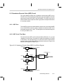
TMS320F/C240 Overview . . . . . . . . . . . . . . . . . . . . . . . . . . . . . . . . . . . . . . . . . . . . . . . . . . . 1-6
TMS320F/C240 DSP Controller . . . . . . . . . . . . . . . . . . . . . . . . . . . . . . . . . . . . . . . . . . . . . . . . . . . 2-1
Describes the TMS320F/C240 DSP Controller. Includes a device overview, pin-out diagram,
memory map, and a discussion on interrupts.
2.1
2.2
2.3
2.4
2.5
2.6
TMS320F/C240 DSP Controller Overview . . . . . . . . . . . . . . . . . . . . . . . . . . . . . . . . . . . . . 2-2
2.1.1 Architectural Overview . . . . . . . . . . . . . . . . . . . . . . . . . . . . . . . . . . . . . . . . . . . . . . 2-13
Memory Map . . . . . . . . . . . . . . . . . . . . . . . . . . . . . . . . . . . . . . . . . . . . . . . . . . . . . . . . . . . . . . 2-15
Peripheral Memory Map . . . . . . . . . . . . . . . . . . . . . . . . . . . . . . . . . . . . . . . . . . . . . . . . . . . . 2-17
Digital I/O and Shared Pin Functions . . . . . . . . . . . . . . . . . . . . . . . . . . . . . . . . . . . . . . . . . 2-19
2.4.1 Description of Group1 Shared I/O pins . . . . . . . . . . . . . . . . . . . . . . . . . . . . . . . . 2-19
2.4.2 Description of Group 2 Shared I/O Pins . . . . . . . . . . . . . . . . . . . . . . . . . . . . . . . 2-22
2.4.3 Digital I/O Control Registers . . . . . . . . . . . . . . . . . . . . . . . . . . . . . . . . . . . . . . . . . 2-22
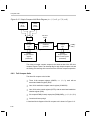
Interrupts . . . . . . . . . . . . . . . . . . . . . . . . . . . . . . . . . . . . . . . . . . . . . . . . . . . . . . . . . . . . . . . . . 2-28
2.5.1 Resets . . . . . . . . . . . . . . . . . . . . . . . . . . . . . . . . . . . . . . . . . . . . . . . . . . . . . . . . . . . . 2-32
2.5.2 Non-Maskable Interrupts (NMI) — Hardware and Software . . . . . . . . . . . . . . . 2-35
2.5.3 Interrupt Structure — Detailed Description . . . . . . . . . . . . . . . . . . . . . . . . . . . . . 2-37
2.5.4 Interrupt Structure — Priority and Ranking . . . . . . . . . . . . . . . . . . . . . . . . . . . . . 2-41
2.5.5 Interrupt Operation: Detailed Description . . . . . . . . . . . . . . . . . . . . . . . . . . . . . . 2-47
2.5.6 Interrupt Latency . . . . . . . . . . . . . . . . . . . . . . . . . . . . . . . . . . . . . . . . . . . . . . . . . . . 2-60
2.5.7 External Interrupts . . . . . . . . . . . . . . . . . . . . . . . . . . . . . . . . . . . . . . . . . . . . . . . . . . 2-62
2.5.8 Peripheral Interrupt Enable Sequence . . . . . . . . . . . . . . . . . . . . . . . . . . . . . . . . . 2-62
2.5.9 Summary of Interrupt Operation . . . . . . . . . . . . . . . . . . . . . . . . . . . . . . . . . . . . . . 2-63
CPU Interrupt Registers . . . . . . . . . . . . . . . . . . . . . . . . . . . . . . . . . . . . . . . . . . . . . . . . . . . . 2-65
2.6.1 External Interrupt Control Registers . . . . . . . . . . . . . . . . . . . . . . . . . . . . . . . . . . . 2-68
xi
Contents
3
System Functions . . . . . . . . . . . . . . . . . . . . . . . . . . . . . . . . . . . . . . . . . . . . . . . . . . . . . . . . . . . . . . . 3-1
Describes ’240 functions that are not specific to any peripheral.
3.1
3.2
3.3
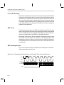
4
PLL Clock Module . . . . . . . . . . . . . . . . . . . . . . . . . . . . . . . . . . . . . . . . . . . . . . . . . . . . . . . . . . . . . . . 4-1
Describes the architecture, functions, and programming of the PLL Clock module.
4.1
4.2
4.3
5
PLL Clock Module Overview . . . . . . . . . . . . . . . . . . . . . . . . . . . . . . . . . . . . . . . . . . . . . . . . . 4-2
PLL Clock Operation . . . . . . . . . . . . . . . . . . . . . . . . . . . . . . . . . . . . . . . . . . . . . . . . . . . . . . . . 4-5
4.2.1 Pin Description . . . . . . . . . . . . . . . . . . . . . . . . . . . . . . . . . . . . . . . . . . . . . . . . . . . . . . 4-5
4.2.2 Oscillator Operation Modes . . . . . . . . . . . . . . . . . . . . . . . . . . . . . . . . . . . . . . . . . . . 4-6
4.2.3 PLL Operation Modes . . . . . . . . . . . . . . . . . . . . . . . . . . . . . . . . . . . . . . . . . . . . . . . . 4-6
4.2.4 CPU Clock (CPUCLK) Frequency Selection . . . . . . . . . . . . . . . . . . . . . . . . . . . . . 4-7
4.2.5 System Clock (SYSCLK) Frequency Selection . . . . . . . . . . . . . . . . . . . . . . . . . . 4-8
4.2.6 Watchdog Counter Clock (WDCLK) . . . . . . . . . . . . . . . . . . . . . . . . . . . . . . . . . . . . 4-9
4.2.7 PLL Startup . . . . . . . . . . . . . . . . . . . . . . . . . . . . . . . . . . . . . . . . . . . . . . . . . . . . . . . . . 4-9
4.2.8 Low-Power Modes . . . . . . . . . . . . . . . . . . . . . . . . . . . . . . . . . . . . . . . . . . . . . . . . . . 4-10
PLL Clock Control Registers . . . . . . . . . . . . . . . . . . . . . . . . . . . . . . . . . . . . . . . . . . . . . . . . 4-14
4.3.1 Clock Control Register 0 (CKCR0) . . . . . . . . . . . . . . . . . . . . . . . . . . . . . . . . . . . . 4-14
4.3.2 Clock Control Register 1 (CKCR1) . . . . . . . . . . . . . . . . . . . . . . . . . . . . . . . . . . . . 4-16
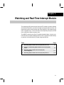
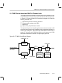
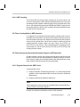
Watchdog and Real-Time Interrupt Module . . . . . . . . . . . . . . . . . . . . . . . . . . . . . . . . . . . . . . . 5-1
Describes the watchdog (WD) and real-time Interrupt (RTI) module. The WD provides interrupts at selected intervals (1 to 4096 interrupts per second), while the RTI is operable by polling
or interrupts. Covers the architecture of both functions as well as the registers used to set up
the functions.
5.1
5.2
xii
Peripheral Interface . . . . . . . . . . . . . . . . . . . . . . . . . . . . . . . . . . . . . . . . . . . . . . . . . . . . . . . . . 3-2
System Configuration Registers . . . . . . . . . . . . . . . . . . . . . . . . . . . . . . . . . . . . . . . . . . . . . . 3-4
3.2.1 System Control Register (SYSCR) . . . . . . . . . . . . . . . . . . . . . . . . . . . . . . . . . . . . . 3-6
3.2.2 System Status Register (SYSSR) . . . . . . . . . . . . . . . . . . . . . . . . . . . . . . . . . . . . . . 3-7
3.2.3 System Interrupt Vector Register (SYSIVR) . . . . . . . . . . . . . . . . . . . . . . . . . . . . . 3-9
Power -Down Modes . . . . . . . . . . . . . . . . . . . . . . . . . . . . . . . . . . . . . . . . . . . . . . . . . . . . . . . 3-10
3.3.1 Clock Generation . . . . . . . . . . . . . . . . . . . . . . . . . . . . . . . . . . . . . . . . . . . . . . . . . . . 3-10
3.3.2 Setting and Entering the Power-Down Modes . . . . . . . . . . . . . . . . . . . . . . . . . . 3-12
3.3.3 Exiting the Power-Down Modes . . . . . . . . . . . . . . . . . . . . . . . . . . . . . . . . . . . . . . 3-12
3.3.4 Low-Power Mode . . . . . . . . . . . . . . . . . . . . . . . . . . . . . . . . . . . . . . . . . . . . . . . . . . . 3-14
3.3.5 After Exiting Power-Down . . . . . . . . . . . . . . . . . . . . . . . . . . . . . . . . . . . . . . . . . . . 3-16
3.3.6 Summary of Power-Down Mode Operation . . . . . . . . . . . . . . . . . . . . . . . . . . . . 3-18
Watchdog (WD) and Real-Time Interrupt (RTI) Overview . . . . . . . . . . . . . . . . . . . . . . . . .
5.1.1 WD and RTI Components . . . . . . . . . . . . . . . . . . . . . . . . . . . . . . . . . . . . . . . . . . . .
5.1.2 Control Registers . . . . . . . . . . . . . . . . . . . . . . . . . . . . . . . . . . . . . . . . . . . . . . . . . . . .
Operation of Watchdog (WD) and Real-Time Interrupt (RTI) Timers . . . . . . . . . . . . . . .
5.2.1 WD Timer . . . . . . . . . . . . . . . . . . . . . . . . . . . . . . . . . . . . . . . . . . . . . . . . . . . . . . . . . .
5.2.2 RTI timer . . . . . . . . . . . . . . . . . . . . . . . . . . . . . . . . . . . . . . . . . . . . . . . . . . . . . . . . . . .
5-2
5-2
5-4
5-6
5-6
5-9
Contents
5.3
5.4
6
Watchdog (WD) and Real-Time Interrupt (RTI) Control Registers . . . . . . . . . . . . . . . .
5.3.1 Real-Time Interrupt Counter Register (RTICNTR) . . . . . . . . . . . . . . . . . . . . . . .
5.3.2 WD Counter Register (WDCNTR) . . . . . . . . . . . . . . . . . . . . . . . . . . . . . . . . . . . .
5.3.3 WD Reset Key Register (WDKEY) . . . . . . . . . . . . . . . . . . . . . . . . . . . . . . . . . . . .
5.3.4 RTI Control Register (RTICR) . . . . . . . . . . . . . . . . . . . . . . . . . . . . . . . . . . . . . . . .
5.3.5 WD Timer Control Register (WDCR) . . . . . . . . . . . . . . . . . . . . . . . . . . . . . . . . . .
Watchdog (WD) and Real-Time Interrupt (RTI) Routines . . . . . . . . . . . . . . . . . . . . . . . .
5-11
5-12
5-13
5-13
5-14
5-16
5-18
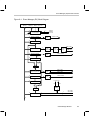
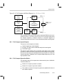
Event Manager Module . . . . . . . . . . . . . . . . . . . . . . . . . . . . . . . . . . . . . . . . . . . . . . . . . . . . . . . . . . . 6-1
Describes the event manager (EV) module. Includes descriptions of the general purpose timer,
compare units, pulse-width modulation waveform circuits, capture units, and quadrature encoder pulse circuits.
6.1
6.2
6.3
6.4
Event Manager (EV) Module Overview . . . . . . . . . . . . . . . . . . . . . . . . . . . . . . . . . . . . . . . . 6-2
6.1.1 EV Functional Blocks . . . . . . . . . . . . . . . . . . . . . . . . . . . . . . . . . . . . . . . . . . . . . . . . 6-2
6.1.2 EV Pins . . . . . . . . . . . . . . . . . . . . . . . . . . . . . . . . . . . . . . . . . . . . . . . . . . . . . . . . . . . . 6-4
6.1.3 Power-Drive Protection . . . . . . . . . . . . . . . . . . . . . . . . . . . . . . . . . . . . . . . . . . . . . . . 6-5
6.1.4 EV Registers . . . . . . . . . . . . . . . . . . . . . . . . . . . . . . . . . . . . . . . . . . . . . . . . . . . . . . . . 6-6
6.1.5 EV Interrupts . . . . . . . . . . . . . . . . . . . . . . . . . . . . . . . . . . . . . . . . . . . . . . . . . . . . . . . . 6-6
Event Manager (EV) Register Addresses . . . . . . . . . . . . . . . . . . . . . . . . . . . . . . . . . . . . . . 6-8
General-Purpose (GP) Timers . . . . . . . . . . . . . . . . . . . . . . . . . . . . . . . . . . . . . . . . . . . . . . . 6-11
6.3.1 GP Timer Functional Blocks . . . . . . . . . . . . . . . . . . . . . . . . . . . . . . . . . . . . . . . . . 6-11
6.3.2 GP Timer Inputs . . . . . . . . . . . . . . . . . . . . . . . . . . . . . . . . . . . . . . . . . . . . . . . . . . . . 6-12
6.3.3 GP Timer Outputs . . . . . . . . . . . . . . . . . . . . . . . . . . . . . . . . . . . . . . . . . . . . . . . . . . 6-13
6.3.4 Control of GP Timer Operation . . . . . . . . . . . . . . . . . . . . . . . . . . . . . . . . . . . . . . . 6-13
6.3.5 GP Timer Control Register (GPTCON) . . . . . . . . . . . . . . . . . . . . . . . . . . . . . . . . 6-13
6.3.6 GP Timer Compare Registers . . . . . . . . . . . . . . . . . . . . . . . . . . . . . . . . . . . . . . . . 6-13
6.3.7 GP Timer Period Register . . . . . . . . . . . . . . . . . . . . . . . . . . . . . . . . . . . . . . . . . . . 6-14
6.3.8 Double Buffering of GP Timer Compare and Period Registers . . . . . . . . . . . . 6-14
6.3.9 GP Timer Compare/PWM Output . . . . . . . . . . . . . . . . . . . . . . . . . . . . . . . . . . . . . 6-15
6.3.10 GP Timer Counting Direction . . . . . . . . . . . . . . . . . . . . . . . . . . . . . . . . . . . . . . . . . 6-15
6.3.11 GP Timer Clock . . . . . . . . . . . . . . . . . . . . . . . . . . . . . . . . . . . . . . . . . . . . . . . . . . . . 6-16
6.3.12 32-Bit Timer . . . . . . . . . . . . . . . . . . . . . . . . . . . . . . . . . . . . . . . . . . . . . . . . . . . . . . . 6-16
6.3.13 QEP-Based Clock Input . . . . . . . . . . . . . . . . . . . . . . . . . . . . . . . . . . . . . . . . . . . . . 6-17
6.3.14 GP Timer Synchronization . . . . . . . . . . . . . . . . . . . . . . . . . . . . . . . . . . . . . . . . . . . 6-17
6.3.15 ADC Start by GP Timer Event . . . . . . . . . . . . . . . . . . . . . . . . . . . . . . . . . . . . . . . . 6-17
6.3.16 GP Timer in Emulation Suspend . . . . . . . . . . . . . . . . . . . . . . . . . . . . . . . . . . . . . . 6-18
6.3.17 GP Timer Interrupts . . . . . . . . . . . . . . . . . . . . . . . . . . . . . . . . . . . . . . . . . . . . . . . . . 6-18
GP Timer Counting Operation . . . . . . . . . . . . . . . . . . . . . . . . . . . . . . . . . . . . . . . . . . . . . . . 6-19
6.4.1 Stop/Hold Mode . . . . . . . . . . . . . . . . . . . . . . . . . . . . . . . . . . . . . . . . . . . . . . . . . . . . 6-19
6.4.2 Single Up Counting Mode . . . . . . . . . . . . . . . . . . . . . . . . . . . . . . . . . . . . . . . . . . . 6-19
6.4.3 Continuous Up Counting Mode . . . . . . . . . . . . . . . . . . . . . . . . . . . . . . . . . . . . . . . 6-22
6.4.4 Directional Up/Down Counting Mode of GP Timers 1 and 3 . . . . . . . . . . . . . . 6-25
6.4.5 Directional Up/Down Counting Mode of GP Timer 2 . . . . . . . . . . . . . . . . . . . . . 6-26
Contents
xiii
Contents
6.5
6.6
6.7
6.8
6.9
6.10
xiv
6.4.6 Single Up/Down Counting Mode . . . . . . . . . . . . . . . . . . . . . . . . . . . . . . . . . . . . . .
6.4.7 Continuous Up/Down Counting Mode . . . . . . . . . . . . . . . . . . . . . . . . . . . . . . . . .
GP Timer Compare Operation . . . . . . . . . . . . . . . . . . . . . . . . . . . . . . . . . . . . . . . . . . . . . . .
6.5.1 Compare/PWM Transition . . . . . . . . . . . . . . . . . . . . . . . . . . . . . . . . . . . . . . . . . . .
6.5.2 Asymmetric/Symmetric Waveform Generator . . . . . . . . . . . . . . . . . . . . . . . . . . .
6.5.3 Asymmetric Waveform Generation . . . . . . . . . . . . . . . . . . . . . . . . . . . . . . . . . . . .
6.5.4 Symmetric Waveform Generation . . . . . . . . . . . . . . . . . . . . . . . . . . . . . . . . . . . . .
6.5.5 Output Logic . . . . . . . . . . . . . . . . . . . . . . . . . . . . . . . . . . . . . . . . . . . . . . . . . . . . . . .
6.5.6 Compare Output in Directional Up/Down Counting Mode . . . . . . . . . . . . . . . .
6.5.7 Active/Inactive Time Calculation . . . . . . . . . . . . . . . . . . . . . . . . . . . . . . . . . . . . . .
GP Timer Control Registers (TxCON and GPTCON) . . . . . . . . . . . . . . . . . . . . . . . . . . .
Generation of Compare and PWM Outputs Using GP Timers . . . . . . . . . . . . . . . . . . . .
6.7.1 Generation of Compare Output . . . . . . . . . . . . . . . . . . . . . . . . . . . . . . . . . . . . . . .
6.7.2 Generation of PWM Output . . . . . . . . . . . . . . . . . . . . . . . . . . . . . . . . . . . . . . . . . .
6.7.3 GP Timer Reset . . . . . . . . . . . . . . . . . . . . . . . . . . . . . . . . . . . . . . . . . . . . . . . . . . . .
Compare Units . . . . . . . . . . . . . . . . . . . . . . . . . . . . . . . . . . . . . . . . . . . . . . . . . . . . . . . . . . . .
6.8.1 Simple Compare Units . . . . . . . . . . . . . . . . . . . . . . . . . . . . . . . . . . . . . . . . . . . . . .
6.8.2 Full Compare Units . . . . . . . . . . . . . . . . . . . . . . . . . . . . . . . . . . . . . . . . . . . . . . . . .
6.8.3 Full Compare Inputs/Outputs . . . . . . . . . . . . . . . . . . . . . . . . . . . . . . . . . . . . . . . . .
6.8.4 Full Compare Operation Modes . . . . . . . . . . . . . . . . . . . . . . . . . . . . . . . . . . . . . .
6.8.5 Compare Mode . . . . . . . . . . . . . . . . . . . . . . . . . . . . . . . . . . . . . . . . . . . . . . . . . . . .
6.8.6 PWM Mode . . . . . . . . . . . . . . . . . . . . . . . . . . . . . . . . . . . . . . . . . . . . . . . . . . . . . . . .
6.8.7 Register Setup for Full Compare Operation . . . . . . . . . . . . . . . . . . . . . . . . . . . .
6.8.8 Compare Unit Registers . . . . . . . . . . . . . . . . . . . . . . . . . . . . . . . . . . . . . . . . . . . . .
6.8.9 Compare Unit Interrupts . . . . . . . . . . . . . . . . . . . . . . . . . . . . . . . . . . . . . . . . . . . . .
6.8.10 Compare Unit Reset . . . . . . . . . . . . . . . . . . . . . . . . . . . . . . . . . . . . . . . . . . . . . . . .
PWM Circuits Associated With Full Compare Units . . . . . . . . . . . . . . . . . . . . . . . . . . . . .
6.9.1 PWM Generation Capability . . . . . . . . . . . . . . . . . . . . . . . . . . . . . . . . . . . . . . . . . .
6.9.2 Programmable Dead-Band Unit . . . . . . . . . . . . . . . . . . . . . . . . . . . . . . . . . . . . . .
6.9.3 Inputs and Outputs of Dead-Band Unit . . . . . . . . . . . . . . . . . . . . . . . . . . . . . . . .
6.9.4 Dead-Band Generation . . . . . . . . . . . . . . . . . . . . . . . . . . . . . . . . . . . . . . . . . . . . . .
6.9.5 Other Important Features of Dead-Band Units . . . . . . . . . . . . . . . . . . . . . . . . . .
6.9.6 Output Logic . . . . . . . . . . . . . . . . . . . . . . . . . . . . . . . . . . . . . . . . . . . . . . . . . . . . . . .
PWM Waveform Generation With Compare Units and PWM Circuits . . . . . . . . . . . . .
6.10.1 PWM Signals . . . . . . . . . . . . . . . . . . . . . . . . . . . . . . . . . . . . . . . . . . . . . . . . . . . . . .
6.10.2 PWM Signal Generation . . . . . . . . . . . . . . . . . . . . . . . . . . . . . . . . . . . . . . . . . . . . .
6.10.3 Dead Band . . . . . . . . . . . . . . . . . . . . . . . . . . . . . . . . . . . . . . . . . . . . . . . . . . . . . . . .
6.10.4 Generation of PWM Outputs With Event Manager . . . . . . . . . . . . . . . . . . . . . .
6.10.5 Asymmetric and Symmetric PWM Generation . . . . . . . . . . . . . . . . . . . . . . . . . .
6.10.6 Register Setup for PWM Generation . . . . . . . . . . . . . . . . . . . . . . . . . . . . . . . . . .
6.10.7 Asymmetric PWM Waveform Generation . . . . . . . . . . . . . . . . . . . . . . . . . . . . . .
6.10.8 Symmetric PWM Waveform Generation . . . . . . . . . . . . . . . . . . . . . . . . . . . . . . .
6-28
6-31
6-34
6-34
6-34
6-35
6-36
6-37
6-38
6-39
6-40
6-45
6-45
6-45
6-46
6-47
6-47
6-48
6-49
6-49
6-50
6-50
6-50
6-51
6-58
6-58
6-59
6-60
6-61
6-62
6-62
6-65
6-67
6-69
6-69
6-69
6-70
6-70
6-70
6-71
6-72
6-73
Contents
6.11
6.12
6.13
6.14
7
Dual 10-Bit Analog-to-Digital Converter (ADC) Module . . . . . . . . . . . . . . . . . . . . . . . . . . . . . 7-1
Describes the Dual 10-Bit Analog-to-Digital Converter (ADC) module.
7.1
7.2
7.3
8
Space-Vector PWM . . . . . . . . . . . . . . . . . . . . . . . . . . . . . . . . . . . . . . . . . . . . . . . . . . . . . . . . 6-74
6.11.1 3-Phase Power Inverter . . . . . . . . . . . . . . . . . . . . . . . . . . . . . . . . . . . . . . . . . . . . . 6-74
6.11.2 Switching Patterns of a Power Inverter and Basic Space Vectors . . . . . . . . . 6-74
6.11.3 Approximation of Motor Voltage with Basic Space Vectors . . . . . . . . . . . . . . . 6-76
6.11.4 Space-Vector PWM Waveform Generation With EV . . . . . . . . . . . . . . . . . . . . . 6-77
6.11.5 Space-Vector PWM Waveforms . . . . . . . . . . . . . . . . . . . . . . . . . . . . . . . . . . . . . . 6-78
6.11.6 Unused Full Compare Register . . . . . . . . . . . . . . . . . . . . . . . . . . . . . . . . . . . . . . . 6-78
6.11.7 Space-Vector PWM Boundary Conditions . . . . . . . . . . . . . . . . . . . . . . . . . . . . . . 6-78
Capture Units . . . . . . . . . . . . . . . . . . . . . . . . . . . . . . . . . . . . . . . . . . . . . . . . . . . . . . . . . . . . . 6-80
6.12.1 Features . . . . . . . . . . . . . . . . . . . . . . . . . . . . . . . . . . . . . . . . . . . . . . . . . . . . . . . . . . 6-81
6.12.2 Operation of Capture Units . . . . . . . . . . . . . . . . . . . . . . . . . . . . . . . . . . . . . . . . . . 6-81
6.12.3 Capture Unit Registers . . . . . . . . . . . . . . . . . . . . . . . . . . . . . . . . . . . . . . . . . . . . . . 6-82
6.12.4 Capture Unit FIFO Stacks (CAPnFIFO, n = 1, 2, 3, 4) . . . . . . . . . . . . . . . . . . . 6-87
Quadrature Encoder Pulse (QEP) Circuit . . . . . . . . . . . . . . . . . . . . . . . . . . . . . . . . . . . . . 6-91
6.13.1 QEP Pins . . . . . . . . . . . . . . . . . . . . . . . . . . . . . . . . . . . . . . . . . . . . . . . . . . . . . . . . . . 6-91
6.13.2 QEP Circuit Time Base . . . . . . . . . . . . . . . . . . . . . . . . . . . . . . . . . . . . . . . . . . . . . . 6-91
6.13.3 QEP Decoding . . . . . . . . . . . . . . . . . . . . . . . . . . . . . . . . . . . . . . . . . . . . . . . . . . . . . 6-92
6.13.4 QEP Counting . . . . . . . . . . . . . . . . . . . . . . . . . . . . . . . . . . . . . . . . . . . . . . . . . . . . . 6-93
6.13.5 Register Setup for the QEP Circuit . . . . . . . . . . . . . . . . . . . . . . . . . . . . . . . . . . . . 6-93
Event Manager (EV) Interrupts . . . . . . . . . . . . . . . . . . . . . . . . . . . . . . . . . . . . . . . . . . . . . . 6-95
6.14.1 Organization of TMS320C240 Interrupts . . . . . . . . . . . . . . . . . . . . . . . . . . . . . . . 6-95
6.14.2 EV Interrupt Requests and Services . . . . . . . . . . . . . . . . . . . . . . . . . . . . . . . . . . 6-95
6.14.3 EV Interrupt Flag Registers . . . . . . . . . . . . . . . . . . . . . . . . . . . . . . . . . . . . . . . . . . 6-99
6.14.4 EV Interrupt Mask Registers . . . . . . . . . . . . . . . . . . . . . . . . . . . . . . . . . . . . . . . . 6-104
6.14.5 EV Interrupt Vector Registers . . . . . . . . . . . . . . . . . . . . . . . . . . . . . . . . . . . . . . . 6-108
Dual 10-Bit ADC Overview . . . . . . . . . . . . . . . . . . . . . . . . . . . . . . . . . . . . . . . . . . . . . . . . . . . 7-2
ADC Operation . . . . . . . . . . . . . . . . . . . . . . . . . . . . . . . . . . . . . . . . . . . . . . . . . . . . . . . . . . . . . 7-4
7.2.1 ADC Module Pin Description . . . . . . . . . . . . . . . . . . . . . . . . . . . . . . . . . . . . . . . . . . 7-4
7.2.2 ADC Module Operational Modes . . . . . . . . . . . . . . . . . . . . . . . . . . . . . . . . . . . . . . 7-4
7.2.3 Analog Signal Sampling/Conversion . . . . . . . . . . . . . . . . . . . . . . . . . . . . . . . . . . . 7-6
ADC Registers . . . . . . . . . . . . . . . . . . . . . . . . . . . . . . . . . . . . . . . . . . . . . . . . . . . . . . . . . . . . . 7-7
7.3.1 ADC Control Register 1 (ADCTRL1) . . . . . . . . . . . . . . . . . . . . . . . . . . . . . . . . . . . 7-7
7.3.2 ADC Control Register 2 (ADCTRL2) . . . . . . . . . . . . . . . . . . . . . . . . . . . . . . . . . . 7-10
7.3.3 ADC Digital Result Registers . . . . . . . . . . . . . . . . . . . . . . . . . . . . . . . . . . . . . . . . . 7-12
Serial Communications Interface (SCI) Module . . . . . . . . . . . . . . . . . . . . . . . . . . . . . . . . . . . 8-1
Describes the architecture, functions, and programming of the serial communications interface
(SCI) module.
8.1
SCI Overview . . . . . . . . . . . . . . . . . . . . . . . . . . . . . . . . . . . . . . . . . . . . . . . . . . . . . . . . . . . . . . 8-2
8.1.1 SCI Physical Description . . . . . . . . . . . . . . . . . . . . . . . . . . . . . . . . . . . . . . . . . . . . . 8-2
8.1.2 Architecture . . . . . . . . . . . . . . . . . . . . . . . . . . . . . . . . . . . . . . . . . . . . . . . . . . . . . . . . . 8-5
Contents
xv
Contents
8.2
8.3
8.4
8.5
8.6
8.7
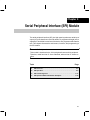
9
Serial Peripheral Interface (SPI) Module . . . . . . . . . . . . . . . . . . . . . . . . . . . . . . . . . . . . . . . . . . . 9-1
Describes the architecture, functions, and programming of the serial peripheral interface (SPI)
module.
9.1
9.2
9.3
xvi
8.1.3 SCI Control Registers . . . . . . . . . . . . . . . . . . . . . . . . . . . . . . . . . . . . . . . . . . . . . . . . 8-5
8.1.4 Multiprocessor and Asynchronous Communications Modes . . . . . . . . . . . . . . . 8-7
SCI Programmable Data Format . . . . . . . . . . . . . . . . . . . . . . . . . . . . . . . . . . . . . . . . . . . . . . 8-8
SCI Multiprocessor Communication . . . . . . . . . . . . . . . . . . . . . . . . . . . . . . . . . . . . . . . . . . . 8-9
8.3.1 Idle-Line Multiprocessor Mode . . . . . . . . . . . . . . . . . . . . . . . . . . . . . . . . . . . . . . . 8-10
8.3.2 Address-Bit Multiprocessor Mode . . . . . . . . . . . . . . . . . . . . . . . . . . . . . . . . . . . . . 8-12
SCI Communication Format . . . . . . . . . . . . . . . . . . . . . . . . . . . . . . . . . . . . . . . . . . . . . . . . . 8-14
8.4.1 Receiver Signals in Communications Modes . . . . . . . . . . . . . . . . . . . . . . . . . . . 8-15
8.4.2 Transmitter Signals in Communications Modes . . . . . . . . . . . . . . . . . . . . . . . . . 8-16
SCI Port Interrupts . . . . . . . . . . . . . . . . . . . . . . . . . . . . . . . . . . . . . . . . . . . . . . . . . . . . . . . . . 8-17
8.5.1 SCI Baud Rate Calculation . . . . . . . . . . . . . . . . . . . . . . . . . . . . . . . . . . . . . . . . . . 8-18
SCI Control Registers . . . . . . . . . . . . . . . . . . . . . . . . . . . . . . . . . . . . . . . . . . . . . . . . . . . . . . 8-19
8.6.1 SCI Communication Control Register (SCICCR) . . . . . . . . . . . . . . . . . . . . . . . . 8-20
8.6.2 SCI Control Register 1 (SCICTL1) . . . . . . . . . . . . . . . . . . . . . . . . . . . . . . . . . . . . 8-22
8.6.3 Baud-Select Registers (SCIHBAUD and SCILBAUD) . . . . . . . . . . . . . . . . . . . . 8-25
8.6.4 SCI Control Register 2 (SCICTL2) . . . . . . . . . . . . . . . . . . . . . . . . . . . . . . . . . . . . 8-26
8.6.5 Receiver Status Register (SCIRXST) . . . . . . . . . . . . . . . . . . . . . . . . . . . . . . . . . . 8-27
8.6.6 Receiver Data Buffer Registers . . . . . . . . . . . . . . . . . . . . . . . . . . . . . . . . . . . . . . . 8-29
8.6.7 Transmit Data Buffer Register (SCITXBUF) . . . . . . . . . . . . . . . . . . . . . . . . . . . . 8-30
8.6.8 Port Control Register 2 (SCIPC2) . . . . . . . . . . . . . . . . . . . . . . . . . . . . . . . . . . . . . 8-31
8.6.9 Priority Control Register (SCIPRI) . . . . . . . . . . . . . . . . . . . . . . . . . . . . . . . . . . . . 8-33
SCI Initialization Example . . . . . . . . . . . . . . . . . . . . . . . . . . . . . . . . . . . . . . . . . . . . . . . . . . . 8-34
SPI Overview . . . . . . . . . . . . . . . . . . . . . . . . . . . . . . . . . . . . . . . . . . . . . . . . . . . . . . . . . . . . . . 9-2
9.1.1 SPI Physical Description . . . . . . . . . . . . . . . . . . . . . . . . . . . . . . . . . . . . . . . . . . . . . 9-2
9.1.2 SPI Control Registers . . . . . . . . . . . . . . . . . . . . . . . . . . . . . . . . . . . . . . . . . . . . . . . . 9-4
SPI Operation . . . . . . . . . . . . . . . . . . . . . . . . . . . . . . . . . . . . . . . . . . . . . . . . . . . . . . . . . . . . . . 9-6
9.2.1 Introduction to Operation . . . . . . . . . . . . . . . . . . . . . . . . . . . . . . . . . . . . . . . . . . . . . 9-6
9.2.2 SPI Module Slave and Master Operation Modes . . . . . . . . . . . . . . . . . . . . . . . . . 9-7
9.2.3 SPI Interrupts . . . . . . . . . . . . . . . . . . . . . . . . . . . . . . . . . . . . . . . . . . . . . . . . . . . . . . . 9-8
9.2.4 Data Format . . . . . . . . . . . . . . . . . . . . . . . . . . . . . . . . . . . . . . . . . . . . . . . . . . . . . . . 9-10
9.2.5 Baud Rate and Clocking Schemes . . . . . . . . . . . . . . . . . . . . . . . . . . . . . . . . . . . . 9-11
9.2.6 Initialization Upon Reset . . . . . . . . . . . . . . . . . . . . . . . . . . . . . . . . . . . . . . . . . . . . . 9-14
9.2.7 Data Transfer Example . . . . . . . . . . . . . . . . . . . . . . . . . . . . . . . . . . . . . . . . . . . . . . 9-15
SPI Control Registers . . . . . . . . . . . . . . . . . . . . . . . . . . . . . . . . . . . . . . . . . . . . . . . . . . . . . . 9-17
9.3.1 SPI Configuration Control Register (SPICCR) . . . . . . . . . . . . . . . . . . . . . . . . . . 9-18
9.3.2 SPI Operation Control Register (SPICTL) . . . . . . . . . . . . . . . . . . . . . . . . . . . . . . 9-20
9.3.3 SPI Status Register (SPISTS) . . . . . . . . . . . . . . . . . . . . . . . . . . . . . . . . . . . . . . . . 9-23
9.3.4 SPI Baud Rate Register (SPIBRR) . . . . . . . . . . . . . . . . . . . . . . . . . . . . . . . . . . . . 9-24
9.3.5 SPI Emulation Buffer Register (SPIEMU) . . . . . . . . . . . . . . . . . . . . . . . . . . . . . . 9-26
9.3.6 SPI Serial Input Buffer Register (SPIBUF) . . . . . . . . . . . . . . . . . . . . . . . . . . . . . 9-27
Contents
9.4
9.3.7 SPI Serial Data Register (SPIDAT) . . . . . . . . . . . . . . . . . . . . . . . . . . . . . . . . . . . .
9.3.8 SPI Port Control Register 1 (SPIPC1) . . . . . . . . . . . . . . . . . . . . . . . . . . . . . . . . .
9.3.9 SPI Port Control Register 2 (SPIPC2) . . . . . . . . . . . . . . . . . . . . . . . . . . . . . . . . .
9.3.10 SPI Priority Control Register (SPIPRI) . . . . . . . . . . . . . . . . . . . . . . . . . . . . . . . . .
SPI Operation-Mode Initialization Examples . . . . . . . . . . . . . . . . . . . . . . . . . . . . . . . . . . .
9-28
9-29
9-31
9-33
9-34
10 Flash Memory Module . . . . . . . . . . . . . . . . . . . . . . . . . . . . . . . . . . . . . . . . . . . . . . . . . . . . . . . . . . 10-1
Describes how the flash EEPROM module is used and how to erase and program the flash
array.
10.1
10.2
10.3
Flash EEPROM Overview . . . . . . . . . . . . . . . . . . . . . . . . . . . . . . . . . . . . . . . . . . . . . . . . . . 10-2
Fundamental Concepts . . . . . . . . . . . . . . . . . . . . . . . . . . . . . . . . . . . . . . . . . . . . . . . . . . . . . 10-3
10.2.1 Erasing . . . . . . . . . . . . . . . . . . . . . . . . . . . . . . . . . . . . . . . . . . . . . . . . . . . . . . . . . . . 10-5
10.2.2 Writing . . . . . . . . . . . . . . . . . . . . . . . . . . . . . . . . . . . . . . . . . . . . . . . . . . . . . . . . . . . . 10-6
Flash Registers . . . . . . . . . . . . . . . . . . . . . . . . . . . . . . . . . . . . . . . . . . . . . . . . . . . . . . . . . . . 10-7
10.3.1 Flash Segment Control Register (SEG_CTR) . . . . . . . . . . . . . . . . . . . . . . . . . . 10-7
10.3.2 Flash Test Register (TST) . . . . . . . . . . . . . . . . . . . . . . . . . . . . . . . . . . . . . . . . . . 10-10
10.3.3 Write Address Register (WADRS) . . . . . . . . . . . . . . . . . . . . . . . . . . . . . . . . . . . 10-10
10.3.4 Write Data Register (WDATA) . . . . . . . . . . . . . . . . . . . . . . . . . . . . . . . . . . . . . . . 10-10
11 External Memory Interface . . . . . . . . . . . . . . . . . . . . . . . . . . . . . . . . . . . . . . . . . . . . . . . . . . . . . . 11-1
Describes the external memory interface, including interface to program memory, local data
memory, and I/O space. Describes the wait-state generator.
11.1
11.2
11.3
11.4
11.5
External Interface to Program Memory . . . . . . . . . . . . . . . . . . . . . . . . . . . . . . . . . . . . . . . 11-2
External Interface to Local Data Memory . . . . . . . . . . . . . . . . . . . . . . . . . . . . . . . . . . . . . . 11-5
Interface to I/O Space . . . . . . . . . . . . . . . . . . . . . . . . . . . . . . . . . . . . . . . . . . . . . . . . . . . . . . 11-8
Memory Interface Timing Diagrams . . . . . . . . . . . . . . . . . . . . . . . . . . . . . . . . . . . . . . . . . 11-10
Wait-State Generator . . . . . . . . . . . . . . . . . . . . . . . . . . . . . . . . . . . . . . . . . . . . . . . . . . . . . . 11-12
11.5.1 Generating Wait States With the READY Signal . . . . . . . . . . . . . . . . . . . . . . . 11-12
11.5.2 Generating Wait States With the Wait-State Generator . . . . . . . . . . . . . . . . . 11-12
12 Digital I/O Ports . . . . . . . . . . . . . . . . . . . . . . . . . . . . . . . . . . . . . . . . . . . . . . . . . . . . . . . . . . . . . . . . 12-1
Describes the digital I/O ports module.
12.1
12.2
12.3
A
Digital I/O Ports Overview . . . . . . . . . . . . . . . . . . . . . . . . . . . . . . . . . . . . . . . . . . . . . . . . . .
Digital I/O and Shared Pin Functions . . . . . . . . . . . . . . . . . . . . . . . . . . . . . . . . . . . . . . . . .
12.2.1 Description of Group1 Shared I/O Pins . . . . . . . . . . . . . . . . . . . . . . . . . . . . . . . .
12.2.2 Description of Group 2 Shared I/O Pins . . . . . . . . . . . . . . . . . . . . . . . . . . . . . . .
Digital I/O Control Registers . . . . . . . . . . . . . . . . . . . . . . . . . . . . . . . . . . . . . . . . . . . . . . . . .
12-2
12-2
12-2
12-5
12-6
Summary of Programmable Registers on the TMS320F/C240 . . . . . . . . . . . . . . . . . . . . . . . A-1
Provides a summary of all programmable registers and shows the individual register configurations.
A.1
A.2
A.3
CPU Registers . . . . . . . . . . . . . . . . . . . . . . . . . . . . . . . . . . . . . . . . . . . . . . . . . . . . . . . . . . . . . A-6
Watchdog (WD) and Real-time Interrupt (RTI) Registers . . . . . . . . . . . . . . . . . . . . . . . . . A-9
PLL Clock Registers . . . . . . . . . . . . . . . . . . . . . . . . . . . . . . . . . . . . . . . . . . . . . . . . . . . . . . . A-11
Contents
xvii
Contents
A.4
A.5
A.6
A.7
A.8
A.9
A.10
A.11
A.12
A.13
A.14
A.15
Dual 10-Bit Analog to Digital Converter (ADC) Registers . . . . . . . . . . . . . . . . . . . . . . . .
Serial Peripheral Interface (SPI) Registers . . . . . . . . . . . . . . . . . . . . . . . . . . . . . . . . . . . .
Serial Communications Interface (SCI) Registers . . . . . . . . . . . . . . . . . . . . . . . . . . . . . .
External Interrupt Control Registers . . . . . . . . . . . . . . . . . . . . . . . . . . . . . . . . . . . . . . . . . .
Digital I/O Control Registers . . . . . . . . . . . . . . . . . . . . . . . . . . . . . . . . . . . . . . . . . . . . . . . . .
General Purpose (GP) Timer Registers . . . . . . . . . . . . . . . . . . . . . . . . . . . . . . . . . . . . . . .
Compare Unit Registers . . . . . . . . . . . . . . . . . . . . . . . . . . . . . . . . . . . . . . . . . . . . . . . . . . . .
Capture Unit Registers . . . . . . . . . . . . . . . . . . . . . . . . . . . . . . . . . . . . . . . . . . . . . . . . . . . . .
Dead-Band Timer Control Register . . . . . . . . . . . . . . . . . . . . . . . . . . . . . . . . . . . . . . . . . . .
Event Manager (EV) Interrupt Registers . . . . . . . . . . . . . . . . . . . . . . . . . . . . . . . . . . . . . .
Flash Control Mode Register—Including Flash Segment Control Register . . . . . . . . .
Wait-State Generator Control Register . . . . . . . . . . . . . . . . . . . . . . . . . . . . . . . . . . . . . . . .
A-12
A-14
A-17
A-20
A-21
A-23
A-28
A-32
A-35
A-36
A-39
A-40
B
Glossary . . . . . . . . . . . . . . . . . . . . . . . . . . . . . . . . . . . . . . . . . . . . . . . . . . . . . . . . . . . . . . . . . . . . . . . . B-1
Explains terms, abbreviations, and acronyms used throughout this book. Glossary.
C
Summary of Updates in This Document . . . . . . . . . . . . . . . . . . . . . . . . . . . . . . . . . . . . . . . . . . . C-1
Provides a summary of the updates in this version of the document.
xviii
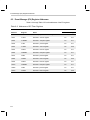
Figures
Figures
1–1
1–2
2–1
2–2
2–3
2–4
2–5
2–6
2–7
2–8
2–9
2–10
2–11
2–12
2–13
2–14
2–15
2–16
2–17
2–18
2–19
2–20
2–21
2–22
2–23
2–24
2–25
3–1
3–2
3–3
3–4
3–5
4–1
4–2
4–3
5–1
TMS320 Family . . . . . . . . . . . . . . . . . . . . . . . . . . . . . . . . . . . . . . . . . . . . . . . . . . . . . . . . . . . . . . . 1-3
TMS320 Device Nomenclature . . . . . . . . . . . . . . . . . . . . . . . . . . . . . . . . . . . . . . . . . . . . . . . . . . 1-3
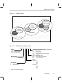
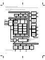
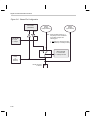
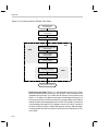
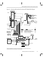
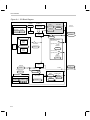
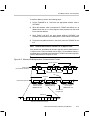
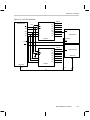
TMS320F/C240 Device Overview . . . . . . . . . . . . . . . . . . . . . . . . . . . . . . . . . . . . . . . . . . . . . . . 2-3
TMS320F/C240 Pin Out Assignment . . . . . . . . . . . . . . . . . . . . . . . . . . . . . . . . . . . . . . . . . . . . 2-4
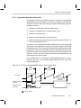
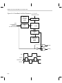
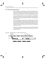
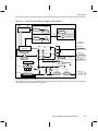
TMS320F/C240 Functional Block Diagram . . . . . . . . . . . . . . . . . . . . . . . . . . . . . . . . . . . . . . 2-14
TMS320F/C240 Memory Map . . . . . . . . . . . . . . . . . . . . . . . . . . . . . . . . . . . . . . . . . . . . . . . . . 2-16
’240 Peripheral Memory Map . . . . . . . . . . . . . . . . . . . . . . . . . . . . . . . . . . . . . . . . . . . . . . . . . . 2-18
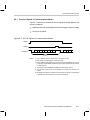
Shared Pin Configuration . . . . . . . . . . . . . . . . . . . . . . . . . . . . . . . . . . . . . . . . . . . . . . . . . . . . . 2-20
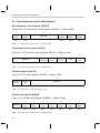
I/O MUX Control Register A (OCRA) — Address 7090h . . . . . . . . . . . . . . . . . . . . . . . . . . . 2-23
I/O MUX Control Register B (OCRB) — Address 7092h . . . . . . . . . . . . . . . . . . . . . . . . . . . 2-24
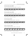
I/O Port A Data and Direction Register (PADATDIR) — Address 7098h . . . . . . . . . . . . . . 2-25
I/O Port B Data and Direction Register (PBDATDIR) — Address 709Ah . . . . . . . . . . . . . 2-26
I/O Port C Data and Direction Register (PCDATDIR) — Address 709Ch . . . . . . . . . . . . . 2-27
Reset Signals . . . . . . . . . . . . . . . . . . . . . . . . . . . . . . . . . . . . . . . . . . . . . . . . . . . . . . . . . . . . . . . 2-32
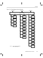
Maskable Interrupt Structure For CPU Interrupt Level 1 . . . . . . . . . . . . . . . . . . . . . . . . . . . 2-39
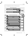
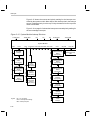
DSP Interrupt Structure . . . . . . . . . . . . . . . . . . . . . . . . . . . . . . . . . . . . . . . . . . . . . . . . . . . . . . . 2-41
System-Module Interrupt Structure . . . . . . . . . . . . . . . . . . . . . . . . . . . . . . . . . . . . . . . . . . . . . 2-42
Event Manager Interrupt Structure . . . . . . . . . . . . . . . . . . . . . . . . . . . . . . . . . . . . . . . . . . . . . . 2-43
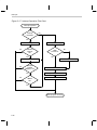
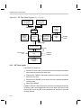
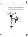
Interrupt Operation Flow Chart . . . . . . . . . . . . . . . . . . . . . . . . . . . . . . . . . . . . . . . . . . . . . . . . . 2-48
Interrupt Service Routine Flow Chart . . . . . . . . . . . . . . . . . . . . . . . . . . . . . . . . . . . . . . . . . . . 2-50
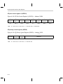
Interrupt Flag Register (IFR) — Address 0006h . . . . . . . . . . . . . . . . . . . . . . . . . . . . . . . . . . 2-66
Interrupt Mask Register (IMR) — Address 0004h . . . . . . . . . . . . . . . . . . . . . . . . . . . . . . . . . 2-68
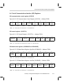
External Interrupt Control Registers . . . . . . . . . . . . . . . . . . . . . . . . . . . . . . . . . . . . . . . . . . . . 2-69
NMI Control Register . . . . . . . . . . . . . . . . . . . . . . . . . . . . . . . . . . . . . . . . . . . . . . . . . . . . . . . . . 2-70
XINT1 Control Register (7070h) . . . . . . . . . . . . . . . . . . . . . . . . . . . . . . . . . . . . . . . . . . . . . . . . 2-71
XINT2 Control Register (7078h) . . . . . . . . . . . . . . . . . . . . . . . . . . . . . . . . . . . . . . . . . . . . . . . . 2-72
XINT3 Control Register (707Ah) . . . . . . . . . . . . . . . . . . . . . . . . . . . . . . . . . . . . . . . . . . . . . . . 2-74
System Configuration Registers . . . . . . . . . . . . . . . . . . . . . . . . . . . . . . . . . . . . . . . . . . . . . . . . 3-5
System Control Register (SYSCR) — Address 7018h . . . . . . . . . . . . . . . . . . . . . . . . . . . . . . 3-6
System Status Register (SYSSR) — Address 701Ah . . . . . . . . . . . . . . . . . . . . . . . . . . . . . . 3-7
System Interrupt Vector Register (SYSIVR) — Address 701Eh . . . . . . . . . . . . . . . . . . . . . . 3-9
Waking Up the Device from Power Down . . . . . . . . . . . . . . . . . . . . . . . . . . . . . . . . . . . . . . . . 3-17
PLL Clock Module Block Diagram . . . . . . . . . . . . . . . . . . . . . . . . . . . . . . . . . . . . . . . . . . . . . . . 4-3
Clock Control Register 0 (CKCR0) — Address 702Bh . . . . . . . . . . . . . . . . . . . . . . . . . . . . . 4-14
Clock Control Register 1 (CKCR1) — Address 702Dh . . . . . . . . . . . . . . . . . . . . . . . . . . . . . 4-16
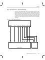
Watchdog (WD) and Real-Time Interrupt (RTI) Module Block Diagram . . . . . . . . . . . . . . . 5-3
Contents
xix
Figures
5–2
5–3
5–4
5–5
5–6
5–7
6–1
6–2
6–3
6–4
6–5
6–6
6–7
6–8
6–9
6–10
6–11
6–12
6–13
6–14
6–15
6–16
6–17
6–18
6–19
6–20
6–21
6–22
6–23
6–24
6–25
6–26
6–27
6–28
6–29
6–30
6–31
6–32
6–33
6–34
6–35
xx
WD/RTI Module Control Registers . . . . . . . . . . . . . . . . . . . . . . . . . . . . . . . . . . . . . . . . . . . . . . 5-11
Real–Time Interrupt Counter Register (RTICNTR) — Address 7021h . . . . . . . . . . . . . . . 5-12
WD Counter Register (WDCNTR) — Address 7023h . . . . . . . . . . . . . . . . . . . . . . . . . . . . . 5-13
WD Reset Key Register (WDKEY) — Address 7025h . . . . . . . . . . . . . . . . . . . . . . . . . . . . . 5-13
RTI Control Register (RTICR) — Address 7027h . . . . . . . . . . . . . . . . . . . . . . . . . . . . . . . . . 5-14
WD Timer Control Register (WDCR) — Address 7029h . . . . . . . . . . . . . . . . . . . . . . . . . . . 5-16
Event Manager (EV) Block Diagram . . . . . . . . . . . . . . . . . . . . . . . . . . . . . . . . . . . . . . . . . . . . . 6-3
GP Timer Block Diagram (x = 1, 2, or 3) . . . . . . . . . . . . . . . . . . . . . . . . . . . . . . . . . . . . . . . . . 6-12
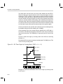
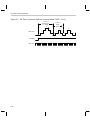
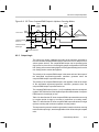
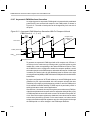
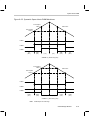
GP Timer Single Up Counting Mode (TxPR = 4 – 1 = 3) . . . . . . . . . . . . . . . . . . . . . . . . . . . 6-20
GP Timer Continuous Up Counting Mode (TxPR = 3 or 2) . . . . . . . . . . . . . . . . . . . . . . . . . 6-23
Directional Up/Down Counting Mode of GP Timers 1 and 3 With Prescale Factor 1
and TxPR = 3 . . . . . . . . . . . . . . . . . . . . . . . . . . . . . . . . . . . . . . . . . . . . . . . . . . . . . . . . . . . . . . . . 6-26
GP Timer Single Up/down Counting Mode (TxPR = 3) . . . . . . . . . . . . . . . . . . . . . . . . . . . . 6-29
GP Timer Continuous Up/Down Counting Mode (TxPR = 3 or 2) . . . . . . . . . . . . . . . . . . . 6-32
GP Timer Compare/PWM Output in Up Counting Mode . . . . . . . . . . . . . . . . . . . . . . . . . . . 6-35
GP Timer Compare/PWM Output in Up/down Counting Modes . . . . . . . . . . . . . . . . . . . . . 6-37
GP Timer Control Register (TxCON; x = 1, 2, and 3) — Addresses 7404h,
7408h, and 740Ch . . . . . . . . . . . . . . . . . . . . . . . . . . . . . . . . . . . . . . . . . . . . . . . . . . . . . . . . . . . 6-40
GP Timer Control Register (GPTCON) — Address 7400h . . . . . . . . . . . . . . . . . . . . . . . . . 6-42
Simple Compare Unit Block Diagram (x = 1, 2, or 3; y = 7, 8, or 9) . . . . . . . . . . . . . . . . . . 6-48
Full Compare Unit Block Diagram (x = 1, 2, 3; y = 1, 3, 5) . . . . . . . . . . . . . . . . . . . . . . . . . 6-49
Compare Control Register (COMCON) — Address 7411h . . . . . . . . . . . . . . . . . . . . . . . . . 6-51
Full Compare Action Control Register (ACTR) — Address 7413h . . . . . . . . . . . . . . . . . . . 6-55
Simple Compare Action Control Register (SACTR) — Address 7414h . . . . . . . . . . . . . . 6-57
PWM Circuits Block Diagram . . . . . . . . . . . . . . . . . . . . . . . . . . . . . . . . . . . . . . . . . . . . . . . . . . 6-59
Dead-Band Timer Control Register (DBTCON) — Address 7415h . . . . . . . . . . . . . . . . . . 6-61
Dead-Band Unit Block Diagram (x = 1, 2, or 3) . . . . . . . . . . . . . . . . . . . . . . . . . . . . . . . . . . . 6-64
Output Logic Block Diagram (x = 1, 2, or 3; y = 1, 2, 3, 4, 5, or 6) . . . . . . . . . . . . . . . . . . . 6-68
Asymmetric PWM Waveform Generation With Full Compare Unit and
PWM Circuits (x = 1, 3, or 5) . . . . . . . . . . . . . . . . . . . . . . . . . . . . . . . . . . . . . . . . . . . . . . . . . . . 6-72
Symmetric PWM Waveform Generation With Full Compare Units and
PWM Circuits (x = 1, 3, or 5) . . . . . . . . . . . . . . . . . . . . . . . . . . . . . . . . . . . . . . . . . . . . . . . . . . . 6-73
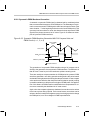
3-Phase Power Inverter Schematic Diagram . . . . . . . . . . . . . . . . . . . . . . . . . . . . . . . . . . . . . 6-74
Basic Space Vectors and Switching Patterns . . . . . . . . . . . . . . . . . . . . . . . . . . . . . . . . . . . . 6-76
Symmetric Space-Vector PWM Waveforms . . . . . . . . . . . . . . . . . . . . . . . . . . . . . . . . . . . . . . 6-79
Capture Units Block Diagram . . . . . . . . . . . . . . . . . . . . . . . . . . . . . . . . . . . . . . . . . . . . . . . . . . 6-80
Capture Control Register (CAPCON) — Address 7420h . . . . . . . . . . . . . . . . . . . . . . . . . . . 6-83
Capture FIFO Status Register (CAPFIFO) — Address 7422h . . . . . . . . . . . . . . . . . . . . . . 6-85
Quadrature Encoder Pulse (QEP) Circuit Block Diagram . . . . . . . . . . . . . . . . . . . . . . . . . . 6-91
Quadrature Encoded Pulses and Decoded Timer Clock and Direction . . . . . . . . . . . . . . . 6-92
EV Interrupt Flag Register A (EVIFRA) — Address 742Fh . . . . . . . . . . . . . . . . . . . . . . . . . 6-99
EV Interrupt Flag Register B (EVIFRB) — Address 7430h . . . . . . . . . . . . . . . . . . . . . . . . 6-101
EV Interrupt Flag Register C (EVIFRC) — Address 7431h . . . . . . . . . . . . . . . . . . . . . . . . 6-103
EV Interrupt Mask Register A (EVIMRA) — Address 742Ch . . . . . . . . . . . . . . . . . . . . . . 6-104
EV Interrupt Mask Register B — Address 742Dh . . . . . . . . . . . . . . . . . . . . . . . . . . . . . . . . 6-106
Figures
6–36
6–37
6–38
6–39
7–1
7–2
7–3
7–4
8–1
8–2
8–3
8–4
8–5
8–6
8–7
8–8
8–9
8–10
8–11
8–12
8–13
8–14
8–15
8–16
8–17
8–18
8–19
8–20
8–21
9–1
9–2
9–3
9–4
9–5
9–6
9–7
9–8
9–9
9–10
9–11
9–12
9–13
EV Interrupt Mask Register C — Address 742Eh . . . . . . . . . . . . . . . . . . . . . . . . . . . . . . . . 6-107
EV Interrupt Vector Register A (EVIVRA) — Address 7432h . . . . . . . . . . . . . . . . . . . . . . 6-108
EV Interrupt Vector Register B (EVIVRB) — Address 7433h . . . . . . . . . . . . . . . . . . . . . . 6-108
EV Interrupt Vector Register C (EVIVRC) — Address 7434h . . . . . . . . . . . . . . . . . . . . . . 6-109
ADC Module Block Diagram . . . . . . . . . . . . . . . . . . . . . . . . . . . . . . . . . . . . . . . . . . . . . . . . . . . . 7-3
ADC Control Register 1 (ADCTRL1) — Address 7032h . . . . . . . . . . . . . . . . . . . . . . . . . . . . 7-7
ADC Control Register 2 (ADCTRL2) — Address 7034h . . . . . . . . . . . . . . . . . . . . . . . . . . . 7-10
ADC Data Registers FIFO1 (ADCFIFO1) — Address 7036h and
FIFO2 (ADCFIFO2) — Address 7038h . . . . . . . . . . . . . . . . . . . . . . . . . . . . . . . . . . . . . . . . . . 7-12
SCI Block Diagram . . . . . . . . . . . . . . . . . . . . . . . . . . . . . . . . . . . . . . . . . . . . . . . . . . . . . . . . . . . 8-4
Typical SCI Data Frame Formats . . . . . . . . . . . . . . . . . . . . . . . . . . . . . . . . . . . . . . . . . . . . . . . . 8-8
Idle-Line Multiprocessor Communication Format . . . . . . . . . . . . . . . . . . . . . . . . . . . . . . . . . 8-10
Double-Buffered WUT and TXSHF . . . . . . . . . . . . . . . . . . . . . . . . . . . . . . . . . . . . . . . . . . . . . 8-11
Address-Bit Multiprocessor Communication Format . . . . . . . . . . . . . . . . . . . . . . . . . . . . . . 8-13
SCI Asynchronous Communications Format . . . . . . . . . . . . . . . . . . . . . . . . . . . . . . . . . . . . . 8-14
SCI RX Signals in Communication Modes . . . . . . . . . . . . . . . . . . . . . . . . . . . . . . . . . . . . . . . 8-15
SCI TX Signals in Communications Modes . . . . . . . . . . . . . . . . . . . . . . . . . . . . . . . . . . . . . . 8-16
SCI Control Registers . . . . . . . . . . . . . . . . . . . . . . . . . . . . . . . . . . . . . . . . . . . . . . . . . . . . . . . . 8-19
SCI Communication Control Register (SCICCR) — Address 7050h . . . . . . . . . . . . . . . . . 8-20
SCI Control Register 1 (SCICTL1) — Address 7051h . . . . . . . . . . . . . . . . . . . . . . . . . . . . . 8-22
SCI Baud-Select MSbyte Register (SCIHBAUD) — Address 7052h . . . . . . . . . . . . . . . . . 8-25
SCI Baud-Select LSbyte Register (SCILBAUD) — Address 7053h . . . . . . . . . . . . . . . . . . 8-25
SCI Control Register 2 (SCICTL2) — Address 7054h . . . . . . . . . . . . . . . . . . . . . . . . . . . . . 8-26
SCI Receiver Status Register (SCIRXST) — Address 7055h . . . . . . . . . . . . . . . . . . . . . . . 8-27
SCIRXST Bit Associations . . . . . . . . . . . . . . . . . . . . . . . . . . . . . . . . . . . . . . . . . . . . . . . . . . . . 8-29
SCI Emulation Data Buffer Register (SCIRXEMU) — Address 7056h . . . . . . . . . . . . . . . 8-30
SCI Receiver Data Buffer Register (SCIRXBUF) — Address 7057h . . . . . . . . . . . . . . . . . 8-30
SCI Transmit Data Buffer Register (SCITXBUF) — Address 7059h . . . . . . . . . . . . . . . . . 8-30
SCI Port Control Register 2 (SCIPC2) — Address 705Eh . . . . . . . . . . . . . . . . . . . . . . . . . . 8-31
SCI Priority Control Register (SCIPRI) — Address 705Fh . . . . . . . . . . . . . . . . . . . . . . . . . 8-33
4-Pin SPI Module Block Diagram (Slave Mode) . . . . . . . . . . . . . . . . . . . . . . . . . . . . . . . . . . . 9-3
SPI Master/Slave Connection (4-Pin Option) . . . . . . . . . . . . . . . . . . . . . . . . . . . . . . . . . . . . . . 9-7
SPICLK Signal Options . . . . . . . . . . . . . . . . . . . . . . . . . . . . . . . . . . . . . . . . . . . . . . . . . . . . . . . 9-13
SPI: SPICLK-SYSCLK Characteristic when (BRR + 1) is Odd, BRR > 3, and
CLOCK POLARITY = 1 . . . . . . . . . . . . . . . . . . . . . . . . . . . . . . . . . . . . . . . . . . . . . . . . . . . . . . . 9-14
Signals Connecting to Master Processor . . . . . . . . . . . . . . . . . . . . . . . . . . . . . . . . . . . . . . . . 9-15
Five Bits per Character . . . . . . . . . . . . . . . . . . . . . . . . . . . . . . . . . . . . . . . . . . . . . . . . . . . . . . . 9-16
SPI Control Registers . . . . . . . . . . . . . . . . . . . . . . . . . . . . . . . . . . . . . . . . . . . . . . . . . . . . . . . . . 9-17
SPI Configuration Control Register (SPICCR) — Address 7040h . . . . . . . . . . . . . . . . . . . 9-18
SPI Operation Control Register (SPICTL) — Address 7041h . . . . . . . . . . . . . . . . . . . . . . . 9-20
SPICLK Signal Options . . . . . . . . . . . . . . . . . . . . . . . . . . . . . . . . . . . . . . . . . . . . . . . . . . . . . . . 9-22
SPI Status Register (SPISTS) — Address 7042h . . . . . . . . . . . . . . . . . . . . . . . . . . . . . . . . . 9-23
SPI Baud Rate Register (SPIBRR) — Address 7044h . . . . . . . . . . . . . . . . . . . . . . . . . . . . . 9-24
SPI Emulation Buffer Register (SPIEMU) — Address 7046h . . . . . . . . . . . . . . . . . . . . . . . 9-26
Contents
xxi
Figures
9–14
9–15
9–16
9–17
9–18
10–1
10–2
11–1
11–2
11–3
11–4
11–5
11–6
12–1
12–2
12–3
12–4
12–5
12–6
A–1
A–2
A–3
A–4
A–5
A–6
A–7
A–8
A–9
A–10
A–11
A–12
A–13
A–14
A–15
A–16
A–17
A–18
A–19
A–20
A–21
A–22
A–23
A–24
A–25
xxii
SPI Serial Input Buffer Register (SPIBUF) — Address 7047h . . . . . . . . . . . . . . . . . . . . . . 9-27
SPI Serial Data Register (SPIDAT) — Address 7049h . . . . . . . . . . . . . . . . . . . . . . . . . . . . . 9-28
SPI Port Control Register 1 (SPIPC1) — Address 704Dh . . . . . . . . . . . . . . . . . . . . . . . . . . 9-29
SPI Port Control Register 2 (SPIPC2) — Address 704Eh . . . . . . . . . . . . . . . . . . . . . . . . . . 9-31
SPI Priority Control Register (SPIPRI) — Address 704Fh . . . . . . . . . . . . . . . . . . . . . . . . . . 9-33
Flash Bit Programming . . . . . . . . . . . . . . . . . . . . . . . . . . . . . . . . . . . . . . . . . . . . . . . . . . . . . . . 10-3
Segment Control Register (SEG_CTR) . . . . . . . . . . . . . . . . . . . . . . . . . . . . . . . . . . . . . . . . . 10-8
Interface to External Program Memory . . . . . . . . . . . . . . . . . . . . . . . . . . . . . . . . . . . . . . . . . . 11-3
Interface to External Data Memory . . . . . . . . . . . . . . . . . . . . . . . . . . . . . . . . . . . . . . . . . . . . . 11-7
I/O Port Interface . . . . . . . . . . . . . . . . . . . . . . . . . . . . . . . . . . . . . . . . . . . . . . . . . . . . . . . . . . . . . 11-9
Memory Interface Read Waveforms . . . . . . . . . . . . . . . . . . . . . . . . . . . . . . . . . . . . . . . . . . . 11-10
Memory Interface Write Waveforms . . . . . . . . . . . . . . . . . . . . . . . . . . . . . . . . . . . . . . . . . . . 11-11
Wait-State Generator Control Register (WSGR) . . . . . . . . . . . . . . . . . . . . . . . . . . . . . . . . . 11-12
Shared Pin Configuration . . . . . . . . . . . . . . . . . . . . . . . . . . . . . . . . . . . . . . . . . . . . . . . . . . . . . 12-3
I/O MUX Control Register A (OCRA) — Address 7090h . . . . . . . . . . . . . . . . . . . . . . . . . . . 12-6
I/O MUX Control Register B (OCRB) — Address 7092h . . . . . . . . . . . . . . . . . . . . . . . . . . . 12-7
I/O Port A Data and Direction Register (PADATDIR) — Address 7098h . . . . . . . . . . . . . . 12-8
I/O Port B Data and Direction Register (PBDATDIR) — Address 709Ah . . . . . . . . . . . . . 12-9
I/O Port C Data and Direction Register (PCDATDIR) — Address 709Ch . . . . . . . . . . . . 12-10
Status Register 0 (ST0) — Internal CPU Register . . . . . . . . . . . . . . . . . . . . . . . . . . . . . . . . . A-6
Status Register 1 (ST1) — Internal CPU Register . . . . . . . . . . . . . . . . . . . . . . . . . . . . . . . . . A-6
Interrupt Mask Register (IMR) — Address 0004h . . . . . . . . . . . . . . . . . . . . . . . . . . . . . . . . . . A-7
Global Memory Allocation Register (GREG) — Address 0005h . . . . . . . . . . . . . . . . . . . . . . A-7
Interrupt Flag Register (IFR) — Address 0006h . . . . . . . . . . . . . . . . . . . . . . . . . . . . . . . . . . . A-7
System Control Register (SYSCR) — Address 7018h . . . . . . . . . . . . . . . . . . . . . . . . . . . . . . A-7
System Status Register (SYSSR) — Address 701Ah . . . . . . . . . . . . . . . . . . . . . . . . . . . . . . A-8
System Interrupt Vector Register (SYSIVR) — Address 701Eh . . . . . . . . . . . . . . . . . . . . . . A-8
Real-Time Interrupt Counter Register (RTICNTR) — Address 7021h . . . . . . . . . . . . . . . . . A-9
Watchdog Counter Register (WDCNTR) — Address 7023h . . . . . . . . . . . . . . . . . . . . . . . . . A-9
Watchdog Reset Key Register (WDKEY) — Address 7025h . . . . . . . . . . . . . . . . . . . . . . . A-10
Real-Time Interrupt Control Register (RTICR) — Address 7027h . . . . . . . . . . . . . . . . . . . A-10
Watchdog Timer Control Register (WDCR) — Address 7029h . . . . . . . . . . . . . . . . . . . . . . A-10
Clock Control Register 0 (CKCR0) — Address 702Bh . . . . . . . . . . . . . . . . . . . . . . . . . . . . . A-11
Clock Control Register 1 (CKCR1) — Address 702Dh . . . . . . . . . . . . . . . . . . . . . . . . . . . . . A-11
ADC Control Register 1 (ADCTRL1) — Address 7032h . . . . . . . . . . . . . . . . . . . . . . . . . . . A-12
ADC Control Register 2 (ADCTRL2) — Address 7034h . . . . . . . . . . . . . . . . . . . . . . . . . . . A-12
ADC Data Register FIFO1 (ADCFIFO1) — Address 7036h . . . . . . . . . . . . . . . . . . . . . . . . A-13
ADC Data Register FIFO2 (ADCFIFO2) — Address 7038h . . . . . . . . . . . . . . . . . . . . . . . . A-13
SPI Configuration Control Register (SPICCR) — Address 7040h . . . . . . . . . . . . . . . . . . . A-14
SPI Operation Control Register (SPICTL) — Address 7041h . . . . . . . . . . . . . . . . . . . . . . . A-14
SPI Status Register (SPISTS) — Address 7042h . . . . . . . . . . . . . . . . . . . . . . . . . . . . . . . . . A-14
SPI Baud Rate Register (SPIBRR) — Address 7044h . . . . . . . . . . . . . . . . . . . . . . . . . . . . . A-14
SPI Emulation Buffer Register (SPIEMU) — Address 7046h . . . . . . . . . . . . . . . . . . . . . . . A-15
SPI Serial Input Buffer Register (SPIBUF) — Address 7047h . . . . . . . . . . . . . . . . . . . . . . A-15
Figures
A–26
A–27
A–28
A–29
A–30
A–31
A–32
A–33
A–34
A–35
A–36
A–37
A–38
A–39
A–40
A–41
A–42
A–43
A–44
A–45
A–46
A–47
A–48
A–49
A–50
A–51
A–52
A–53
A–54
A–55
A–56
A–57
A–58
A–59
A–60
A–61
A–62
A–63
A–64
A–65
A–66
A–67
A–68
A–69
SPI Serial Data Register (SPIDAT) — Address 7049h . . . . . . . . . . . . . . . . . . . . . . . . . . . . .
SPI Port Control Register 1 (SPIPC1) — Address 704Dh . . . . . . . . . . . . . . . . . . . . . . . . . .
SPI Port Control Register 2 (SPIPC2) — Address 704Eh . . . . . . . . . . . . . . . . . . . . . . . . . .
SPI Priority Control Register (SPIPRI) — Address 704Fh . . . . . . . . . . . . . . . . . . . . . . . . . .
SCI Communication Control Register (SCICCR) — Address 7050h . . . . . . . . . . . . . . . . .
SCI Control Register 1 (SCICTL1) — Address 7051h . . . . . . . . . . . . . . . . . . . . . . . . . . . . .
SCI Baud-Select Register, High Bits (SCIHBAUD) — Address 7052h . . . . . . . . . . . . . . .
SCI Baud-Select Register, Low Bits (SCILBAUD) — Address 7053h . . . . . . . . . . . . . . . .
SCI Control Register 2 (SCICTL2) — Address 7054h . . . . . . . . . . . . . . . . . . . . . . . . . . . . .
SCI Receiver Status Register (SCIRXST) — Address 7055h . . . . . . . . . . . . . . . . . . . . . . .
SCI Emulation Data Buffer Register (SCIRXEMU) — Address 7056h . . . . . . . . . . . . . . .
SCI Receiver Data Buffer Register (SCIRXBUF) — Address 7057h . . . . . . . . . . . . . . . . .
SCI Transmit Data Buffer Register (SCITXBUF) — Address 7059h . . . . . . . . . . . . . . . . .
SCI Port Control Register 2 (SCIPC2) — Address 705Eh . . . . . . . . . . . . . . . . . . . . . . . . . .
SCI Priority Control Register (SCIPRI) — Address 705Fh . . . . . . . . . . . . . . . . . . . . . . . . .
External Interrupt 1 Control Register (XINT1CR) — Address 7070h . . . . . . . . . . . . . . . . .
Nonmaskable Interrupt Control Register (NMICR) — Address 7072h . . . . . . . . . . . . . . .
External Interrupt 2 Control Register (XINT2CR) — Address 7078h . . . . . . . . . . . . . . . . .
External Interrupt 3 Control Register (XINT3CR) — Address 707Ah . . . . . . . . . . . . . . . .
I/O MUX Control Register A (OCRA) — Address 7090h . . . . . . . . . . . . . . . . . . . . . . . . . . .
I/O MUX Control Register B (OCRB) — Address 7092h . . . . . . . . . . . . . . . . . . . . . . . . . . .
I/O Port A Data and Direction Register (PADATDIR) — Address 7098h . . . . . . . . . . . . . .
I/O Port B Data and Direction Register (PBDATDIR) — Address 709Ah . . . . . . . . . . . . .
I/O Port C Data and Direction Register (PCDATDIR) — Address 709Ch . . . . . . . . . . . . .
GP Timer Control Register (GPTCON) — Address 7400h . . . . . . . . . . . . . . . . . . . . . . . . .
GP Timer 1 Counter Register (T1CNT) — Address 7401h . . . . . . . . . . . . . . . . . . . . . . . . .
GP Timer 1 Compare Register (T1CMPR) — Address 7402h . . . . . . . . . . . . . . . . . . . . . .
GP Timer 1 Period Register (T1PR) — Address 7403h . . . . . . . . . . . . . . . . . . . . . . . . . . . .
GP Timer 1 Control Register (T1CON) — Address 7404h . . . . . . . . . . . . . . . . . . . . . . . . .
GP Timer 2 Counter Register (T2CNT) — Address 7405h . . . . . . . . . . . . . . . . . . . . . . . . .
GP Timer 2 Compare Register (T2CMPR) — Address 7406h . . . . . . . . . . . . . . . . . . . . . .
GP Timer 2 Period Register (T2PR) — Address 7407h . . . . . . . . . . . . . . . . . . . . . . . . . . . .
GP Timer 2 Control Register (T2CON) — Address 7408h . . . . . . . . . . . . . . . . . . . . . . . . .
GP Timer 3 Counter Register (T3CNT) — Address 7409h . . . . . . . . . . . . . . . . . . . . . . . . .
GP Timer 3 Compare Register (T3CMPR) — Address 740Ah . . . . . . . . . . . . . . . . . . . . . .
GP Timer 3 Period Register (T3PR) — Address 740Bh . . . . . . . . . . . . . . . . . . . . . . . . . . .
GP Timer 3 Control Register (T3CON) — Address 740Ch . . . . . . . . . . . . . . . . . . . . . . . . .
Compare Control Register (COMCON) — Address 7411h . . . . . . . . . . . . . . . . . . . . . . . . .
Full-Compare Action Control Register (ACTR) — Address 7413h . . . . . . . . . . . . . . . . . . .
Full-Compare Unit Compare Register 1 (CMPR1) — Address 7417h . . . . . . . . . . . . . . . .
Full-Compare Unit Compare Register 2 (CMPR2) — Address 7418h . . . . . . . . . . . . . . . .
Full-Compare Unit Compare Register 3 (CMPR3) — Address 7419h . . . . . . . . . . . . . . . .
Simple-Compare Action Control Register (SACTR) — Address 7414h . . . . . . . . . . . . . .
Simple-Compare Unit Compare Register 1 (SCMPR1) — Address 741Ah . . . . . . . . . . .
Contents
A-15
A-15
A-16
A-16
A-17
A-17
A-17
A-17
A-18
A-18
A-18
A-18
A-19
A-19
A-19
A-20
A-20
A-20
A-20
A-21
A-21
A-22
A-22
A-22
A-23
A-23
A-24
A-24
A-24
A-25
A-25
A-25
A-26
A-26
A-26
A-27
A-27
A-28
A-28
A-29
A-29
A-29
A-30
A-30
xxiii
Figures
A–70
A–71
A–72
A–73
A–74
A–75
A–76
A–77
A–78
A–79
A–80
A–81
A–82
A–83
A–84
A–85
A–86
A–87
A–88
A–89
A–90
xxiv
Simple-Compare Unit Compare Register 2 (SCMPR2) — Address 741Bh . . . . . . . . . . .
Simple-Compare Unit Compare Register 3 (SCMPR3) — Address 741Ch . . . . . . . . . . .
Capture Control Register (CAPCON) — Address 7420h . . . . . . . . . . . . . . . . . . . . . . . . . . .
Capture FIFO Status Register (CAPFIFO) — Address 7422h . . . . . . . . . . . . . . . . . . . . . .
Capture 1 FIFO Stack Register (CAP1FIFO) — Address 7423h . . . . . . . . . . . . . . . . . . . .
Capture 2 FIFO Stack Register (CAP2FIFO) — Address 7424h . . . . . . . . . . . . . . . . . . . .
Capture 3 FIFO Stack Register (CAP3FIFO) — Address 7425h . . . . . . . . . . . . . . . . . . . .
Capture 4 FIFO Stack Register (CAP4FIFO) — Address 7426h . . . . . . . . . . . . . . . . . . . .
Dead-Band Timer Control Register (DBTCON) — Address 7415h . . . . . . . . . . . . . . . . . .
EV Interrupt Mask Register A (EVIMRA) — Address 742Ch . . . . . . . . . . . . . . . . . . . . . . .
EV Interrupt Mask Register B (EVIMRB) — Address 742Dh . . . . . . . . . . . . . . . . . . . . . . .
EV Interrupt Mask Register C (EVIMRC) — Address 742Eh . . . . . . . . . . . . . . . . . . . . . . .
EV Interrupt Flag Register A (EVIFRA) — Address 742Fh . . . . . . . . . . . . . . . . . . . . . . . . .
EV Interrupt Flag Register B (EVIFRB) — Address 7430h . . . . . . . . . . . . . . . . . . . . . . . . .
EV Interrupt Flag Register C (EVIFRC) — Address 7431h . . . . . . . . . . . . . . . . . . . . . . . . .
EV Interrupt Vector Register A (EVIVRA) — Address 7432h . . . . . . . . . . . . . . . . . . . . . . .
EV Interrupt Vector Register B (EVIVRB) — Address 7433h . . . . . . . . . . . . . . . . . . . . . . .
EV Interrupt Vector Register C (EVIVRC) — Address 7434h . . . . . . . . . . . . . . . . . . . . . . .
Flash Control Mode Register (FCMR) — I/O Space Address FF0Fh . . . . . . . . . . . . . . . .
Segment Control Register (SEG_CTR) — Program Space Address 0h . . . . . . . . . . . . . .
Wait-State Generator Control Register (WSGR) — I/O Space
Address FFFFh . . . . . . . . . . . . . . . . . . . . . . . . . . . . . . . . . . . . . . . . . . . . . . . . . . . . . . . . . . . . . .
A-30
A-31
A-32
A-32
A-33
A-33
A-33
A-34
A-35
A-36
A-36
A-36
A-37
A-37
A-37
A-38
A-38
A-38
A-39
A-39
A-40
Tables
Tables
2–1
2–2
2–3
2–4
2–5
2–6
2–7
2–8
2–9
2–10
2–11
2–12
2–13
2–14
2–15
2–16
3–1
3–2
3–3
3–4
3–5
3–6
4–1
4–2
4–3
4–4
4–5
4–6
4–7
4–8
4–9
5–1
5–2
5–3
5–4
6–1
Characteristics of the TMS320F/C240 DSP Controllers . . . . . . . . . . . . . . . . . . . . . . . . . . . . 2-2
TMS320F/C240 Pin Functions . . . . . . . . . . . . . . . . . . . . . . . . . . . . . . . . . . . . . . . . . . . . . . . . . 2-5
TMS320F/C240 Shared Pin Configuration . . . . . . . . . . . . . . . . . . . . . . . . . . . . . . . . . . . . . . . 2-21
Group 2 Shared Pins . . . . . . . . . . . . . . . . . . . . . . . . . . . . . . . . . . . . . . . . . . . . . . . . . . . . . . . . . 2-22
Addresses of Digital I/O Control Registers . . . . . . . . . . . . . . . . . . . . . . . . . . . . . . . . . . . . . . . 2-22
I/O MUX Control Register A (OCRA) Configuration . . . . . . . . . . . . . . . . . . . . . . . . . . . . . . . 2-23
I/O MUX Control Register B (OCRB) Configuration . . . . . . . . . . . . . . . . . . . . . . . . . . . . . . . 2-24
’240 DSP Core Interrupt Locations and Priorities . . . . . . . . . . . . . . . . . . . . . . . . . . . . . . . . . 2-30
Interrupt Priorities at the Level of the DSP Core . . . . . . . . . . . . . . . . . . . . . . . . . . . . . . . . . . 2-37
Interrupt Lines Controlled by the System Module and Event Manager . . . . . . . . . . . . . . . 2-38
’240 Interrupt Locations and Priorities . . . . . . . . . . . . . . . . . . . . . . . . . . . . . . . . . . . . . . . . . . 2-45
’240 Maskable Interrupt Vector Table . . . . . . . . . . . . . . . . . . . . . . . . . . . . . . . . . . . . . . . . . . . 2-51
Example of Method 1 ISR . . . . . . . . . . . . . . . . . . . . . . . . . . . . . . . . . . . . . . . . . . . . . . . . . . . . . 2-53
Example of Method 2 ISR . . . . . . . . . . . . . . . . . . . . . . . . . . . . . . . . . . . . . . . . . . . . . . . . . . . . . 2-55
Example of Method 3 ISR . . . . . . . . . . . . . . . . . . . . . . . . . . . . . . . . . . . . . . . . . . . . . . . . . . . . . 2-57
Implementation of an ISR for NMI . . . . . . . . . . . . . . . . . . . . . . . . . . . . . . . . . . . . . . . . . . . . . . 2-58
CPU Cycles to Complete Reads From and Writes to the Peripheral Bus . . . . . . . . . . . . . . 3-3
Power-Down Modes . . . . . . . . . . . . . . . . . . . . . . . . . . . . . . . . . . . . . . . . . . . . . . . . . . . . . . . . . . 3-12
Setting the Power-Down Mode With the PLLPM Bits . . . . . . . . . . . . . . . . . . . . . . . . . . . . . . 3-12
Low Power Modes . . . . . . . . . . . . . . . . . . . . . . . . . . . . . . . . . . . . . . . . . . . . . . . . . . . . . . . . . . . 3-14
Power-Down Modes and Their Terminations . . . . . . . . . . . . . . . . . . . . . . . . . . . . . . . . . . . . . 3-15
External Interrupt Types and Functions . . . . . . . . . . . . . . . . . . . . . . . . . . . . . . . . . . . . . . . . . 3-19
Addresses of PLL Clock Module Control Registers . . . . . . . . . . . . . . . . . . . . . . . . . . . . . . . . 4-4
Oscillator Operation Mode Selection . . . . . . . . . . . . . . . . . . . . . . . . . . . . . . . . . . . . . . . . . . . . . 4-6
Selectable CPU Clock Frequencies in MHz . . . . . . . . . . . . . . . . . . . . . . . . . . . . . . . . . . . . . . . 4-8
PLL Prescale Selection Options . . . . . . . . . . . . . . . . . . . . . . . . . . . . . . . . . . . . . . . . . . . . . . . . . 4-8
Watchdog Counter Clock Frequencies . . . . . . . . . . . . . . . . . . . . . . . . . . . . . . . . . . . . . . . . . . . 4-9
Low-Power Modes . . . . . . . . . . . . . . . . . . . . . . . . . . . . . . . . . . . . . . . . . . . . . . . . . . . . . . . . . . . 4-11
CLKMD(1:0) Bits vs. Clock Mode . . . . . . . . . . . . . . . . . . . . . . . . . . . . . . . . . . . . . . . . . . . . . . . 4-14
CKINF(3:0) Bits vs. Clock-In Frequency (Internal CPU Clock) . . . . . . . . . . . . . . . . . . . . . . 4-16
PLLFB(2:0) Bits vs. PLL Multiplication Ratio . . . . . . . . . . . . . . . . . . . . . . . . . . . . . . . . . . . . . 4-17
Addresses of WD/RTI Module Registers . . . . . . . . . . . . . . . . . . . . . . . . . . . . . . . . . . . . . . . . . 5-5
Typical WDKEY Register Power -up Sequence . . . . . . . . . . . . . . . . . . . . . . . . . . . . . . . . . . . 5-7
Real-Time Interrupt Selections . . . . . . . . . . . . . . . . . . . . . . . . . . . . . . . . . . . . . . . . . . . . . . . . . 5-15
WD Overflow (Timeout) Selections . . . . . . . . . . . . . . . . . . . . . . . . . . . . . . . . . . . . . . . . . . . . . 5-17
EV Pins . . . . . . . . . . . . . . . . . . . . . . . . . . . . . . . . . . . . . . . . . . . . . . . . . . . . . . . . . . . . . . . . . . . . . . 6-5
Contents
xxv
Tables
6–2
6–3
6–4
6–5
6–6
6–7
6–8
6–9
6–10
7–1
7–2
8–1
8–2
8–3
8–4
8–5
9–1
9–2
9–3
10–1
11–1
11–2
12–1
12–2
12–3
12–4
12–5
A–1
xxvi
Addresses of GP Timer Registers . . . . . . . . . . . . . . . . . . . . . . . . . . . . . . . . . . . . . . . . . . . . . . . 6-8
Addresses of Full and Simple Compare Unit Registers . . . . . . . . . . . . . . . . . . . . . . . . . . . . . 6-9
Addresses of Capture Unit and Quadrature Encoder Pulse Decoding
Circuit Registers . . . . . . . . . . . . . . . . . . . . . . . . . . . . . . . . . . . . . . . . . . . . . . . . . . . . . . . . . . . . . . 6-9
Addresses of EV Interrupt Registers . . . . . . . . . . . . . . . . . . . . . . . . . . . . . . . . . . . . . . . . . . . . 6-10
GP Timer Compare/PWM Output in Single Up and Continuous Up Counting Modes . . 6-38
GP Timer Compare/PWM Output in Single Up/Down and Continuous Up/Down
Counting Modes . . . . . . . . . . . . . . . . . . . . . . . . . . . . . . . . . . . . . . . . . . . . . . . . . . . . . . . . . . . . . 6-38
Dead-Band Generation Examples . . . . . . . . . . . . . . . . . . . . . . . . . . . . . . . . . . . . . . . . . . . . . . 6-63
Switching Patterns of a 3-Phase Power Inverter . . . . . . . . . . . . . . . . . . . . . . . . . . . . . . . . . . 6-75
Event Manager Interrupts . . . . . . . . . . . . . . . . . . . . . . . . . . . . . . . . . . . . . . . . . . . . . . . . . . . . . 6-97
Sample Clock Frequencies and Appropriate Prescaler Values . . . . . . . . . . . . . . . . . . . . . . . 7-6
Addresses of ADC Registers . . . . . . . . . . . . . . . . . . . . . . . . . . . . . . . . . . . . . . . . . . . . . . . . . . . 7-7
Addresses of SCI Registers . . . . . . . . . . . . . . . . . . . . . . . . . . . . . . . . . . . . . . . . . . . . . . . . . . . . 8-6
Programming the Data Format Using SCICCR . . . . . . . . . . . . . . . . . . . . . . . . . . . . . . . . . . . . 8-8
Asynchronous Baud Register Values for Common SCI Bit Rates . . . . . . . . . . . . . . . . . . . 8-18
SCI CHAR2 — 0 Bit Values and Character Lengths . . . . . . . . . . . . . . . . . . . . . . . . . . . . . . . 8-21
SW RESET-Affected Flags . . . . . . . . . . . . . . . . . . . . . . . . . . . . . . . . . . . . . . . . . . . . . . . . . . . . 8-23
Addresses of SPI Control Registers . . . . . . . . . . . . . . . . . . . . . . . . . . . . . . . . . . . . . . . . . . . . . 9-5
SPI Clocking Scheme Selection Guide . . . . . . . . . . . . . . . . . . . . . . . . . . . . . . . . . . . . . . . . . . 9-13
Character Length Control Bit Values . . . . . . . . . . . . . . . . . . . . . . . . . . . . . . . . . . . . . . . . . . . . 9-19
Addresses of Flash EEPROM Module Registers . . . . . . . . . . . . . . . . . . . . . . . . . . . . . . . . . 10-7
Key Signals for External Interfacing to Program Memory . . . . . . . . . . . . . . . . . . . . . . . . . . 11-2
Key Signals for External Interfacing to Local Data Memory . . . . . . . . . . . . . . . . . . . . . . . . 11-5
TMS320C240 Shared Pin Configuration . . . . . . . . . . . . . . . . . . . . . . . . . . . . . . . . . . . . . . . . . 12-4
Group 2 Shared Pins . . . . . . . . . . . . . . . . . . . . . . . . . . . . . . . . . . . . . . . . . . . . . . . . . . . . . . . . . 12-5
Addresses of Digital I/O Control Registers . . . . . . . . . . . . . . . . . . . . . . . . . . . . . . . . . . . . . . . 12-6
I/O MUX Control Register A (OCRA) Configuration . . . . . . . . . . . . . . . . . . . . . . . . . . . . . . . 12-7
I/O MUX Control Register B (OCRB) Configuration . . . . . . . . . . . . . . . . . . . . . . . . . . . . . . . 12-8
Addresses of TMS320F/C240 Registers . . . . . . . . . . . . . . . . . . . . . . . . . . . . . . . . . . . . . . . . . A-2
Examples
Examples
5–1
5–2
6–1
6–2
6–3
6–4
6–5
6–6
6–7
6–8
6–9
7–1
8–1
9–1
9–2
9–3
9–4
11–1
11–2
Watchdog (WD) and Real-Time Interrupt (RTI) Enable Routine . . . . . . . . . . . . . . . . . . . . .
Watchdog (WD) and Real-Time Interrupt (RTI) Disable Routine . . . . . . . . . . . . . . . . . . . .
Initialization Routine for Single Up Counting Mode . . . . . . . . . . . . . . . . . . . . . . . . . . . . . . . .
Initialization Routine for Continuous Up Counting Mode . . . . . . . . . . . . . . . . . . . . . . . . . . .
Initialization Routine for Directional Up/down Counting Mode Using
An External Clock . . . . . . . . . . . . . . . . . . . . . . . . . . . . . . . . . . . . . . . . . . . . . . . . . . . . . . . . . . . .
Initialization Routine for Single Up/Down Counting Mode . . . . . . . . . . . . . . . . . . . . . . . . . .
Initialization Routine for the Continuous Up/Down Counting Mode . . . . . . . . . . . . . . . . . .
of COMCON Configuration for Full Compare Units in PWM Mode . . . . . . . . . . . . . . . . . .
Initialization Routine for Dead-Band Generation . . . . . . . . . . . . . . . . . . . . . . . . . . . . . . . . . .
Initialization Routine for Capture Units . . . . . . . . . . . . . . . . . . . . . . . . . . . . . . . . . . . . . . . . . .
Register Setup for a QEP Circuit . . . . . . . . . . . . . . . . . . . . . . . . . . . . . . . . . . . . . . . . . . . . . . .
ADC Initialization . . . . . . . . . . . . . . . . . . . . . . . . . . . . . . . . . . . . . . . . . . . . . . . . . . . . . . . . . . . .
Asynchronous Communication Routine . . . . . . . . . . . . . . . . . . . . . . . . . . . . . . . . . . . . . . . . .
Transmission of Bit from SPIBUF . . . . . . . . . . . . . . . . . . . . . . . . . . . . . . . . . . . . . . . . . . . . . . .
Maximum Baud-Rate Calculation . . . . . . . . . . . . . . . . . . . . . . . . . . . . . . . . . . . . . . . . . . . . . . .
TMS320x240 SPI Slave Mode Code . . . . . . . . . . . . . . . . . . . . . . . . . . . . . . . . . . . . . . . . . . . .
TMS320x240 SPI Master Mode Code . . . . . . . . . . . . . . . . . . . . . . . . . . . . . . . . . . . . . . . . . . .
External I/O Port Access . . . . . . . . . . . . . . . . . . . . . . . . . . . . . . . . . . . . . . . . . . . . . . . . . . . . . .
I/O-Mapped Register Access . . . . . . . . . . . . . . . . . . . . . . . . . . . . . . . . . . . . . . . . . . . . . . . . . .
Contents
5-18
5-19
6-21
6-24
6-27
6-30
6-33
6-54
6-66
6-88
6-94
7-13
8-34
9-10
9-12
9-34
9-40
11-8
11-8
xxvii
Notes, Cautions, and Warnings
Notes, Cautions, and Warnings
Sharing device pins . . . . . . . . . . . . . . . . . . . . . . . . . . . . . . . . . . . . . . . . . . . . . . . . . . . . . . . . . . . . . . . . . . . 6-2
Initialize period registers, compare register transparency . . . . . . . . . . . . . . . . . . . . . . . . . . . . . . . . . 6-15
Synchronization of the GP Timers . . . . . . . . . . . . . . . . . . . . . . . . . . . . . . . . . . . . . . . . . . . . . . . . . . . . . 6-42
Shoot-Through Fault . . . . . . . . . . . . . . . . . . . . . . . . . . . . . . . . . . . . . . . . . . . . . . . . . . . . . . . . . . . . . . . . . 6-62
Clearing Interrupt Flags in EVIFx . . . . . . . . . . . . . . . . . . . . . . . . . . . . . . . . . . . . . . . . . . . . . . . . . . . . . . 6-98
Address-Bit Format for Transfers of 11 Bytes or Less . . . . . . . . . . . . . . . . . . . . . . . . . . . . . . . . . . . . 8-13
Do Not Change Configuration when SW RESET bit = 1 . . . . . . . . . . . . . . . . . . . . . . . . . . . . . . . . . . 8-22
Register Bit Naming Protocol . . . . . . . . . . . . . . . . . . . . . . . . . . . . . . . . . . . . . . . . . . . . . . . . . . . . . . . . . . 9-6
Proper SPI Initialization Using the SPI SW RESET Bit . . . . . . . . . . . . . . . . . . . . . . . . . . . . . . . . . . . . 9-14
Reading the SPIBUF . . . . . . . . . . . . . . . . . . . . . . . . . . . . . . . . . . . . . . . . . . . . . . . . . . . . . . . . . . . . . . . . 9-27
Segment Protection . . . . . . . . . . . . . . . . . . . . . . . . . . . . . . . . . . . . . . . . . . . . . . . . . . . . . . . . . . . . . . . . . 10-8
xxviii
Chapter 1
Introduction
The TMS320C24x (’C24x) series is a member of the TMS320 family of digital
signal processors (DSPs). The ’C24x series is designed to meet a wide range
of digital motor control (DMC) and embedded control applications.
This reference guide discusses the peripherals available on the
TMS320F240/C240 DSP controllers. For a description of the ’C2xx CPU core
and instruction set, refer to TMS320F/C24x DSP Controllers, CPU and Instruction Set Reference Guide (literature number SPRU160).
This chapter provides an overview of the current TMS320 family, describes the
background and benefits of the ’C24x DSP controller products, and introduces
the ’F/C240 device.
Topic
Page
1.1
TMS320 Family Overview . . . . . . . . . . . . . . . . . . . . . . . . . . . . . . . . . . . . . . 1-2
1.2
TMS320C24x Series of DSP Controllers . . . . . . . . . . . . . . . . . . . . . . . . . 1-4
1.3
TMS320F/C240 Overview . . . . . . . . . . . . . . . . . . . . . . . . . . . . . . . . . . . . . . 1-6
Introduction
1-1
TMS320 Family Overview
1.1 TMS320 Family Overview
The TMS320 family consists of fixed-point, floating-point, multiprocessor digital signal processors (DSPs), and fixed-point DSP controllers. TMS320 DSPs
have an architecture designed specifically for real-time signal processing. The
’F/C240 is a member of the ’C2000 DSP platform, and is optimized for control
applications. The ’C24x series of DSP controllers combines this real-time
processing capability with controller peripherals to create an ideal solution for
control system applications. The following characteristics make the TMS320
family the right choice for a wide range of processing applications:
-
Very flexible instruction set
Inherent operational flexibility
High-speed performance
Innovative parallel architecture
Cost effectiveness
In 1982, Texas Instruments introduced the TMS32010, the first fixed-point
DSP in the TMS320 family. Before the end of the year, Electronic Products
magazine awarded the TMS32010 the title “Product of the Year”. Today, the
TMS320 family consists of these generations (Figure 1–1): ’C1x, ’C2x, ’C2xx,
’C5x, ’C54x, and ’C6x fixed-point DSPs; ’C3x and ’C4x floating-point DSPs;
and ’C8x multiprocessor DSPs. The ’C24x is part of the ’C2xx family of DSPs
designed using the 2xLP DSP core.
Devices within a generation of the TMS320 family have the same CPU structure but different on-chip memory and peripheral configurations. Spin-off
devices use new combinations of on-chip memory and peripherals to satisfy
a wide range of needs in the worldwide electronics market. By integrating
memory and peripherals onto a single chip, TMS320 devices reduce system
costs and save circuit board space.
1-2
TMS320 Family Overview
Figure 1–1. TMS320 Family
’C6000
(’C62x, ’C67x)
’C5000
(’C54x)
’C2000
(’C20x, ’C24x)
’C5x
’C8x
’C3x/4x
High performance
Power-efficient
performance
’C1/2x
Control optimized
Figure 1–2. TMS320 Device Nomenclature
TMS 320 C 240 PQ
PREFIX
TMX = Experimental device
TMP = Prototype device
TMS = Qualified device
DEVICE FAMILY
320 = TMS320 Family
TECHNOLOGY
C = ROM
F = Flash EEPROM
(L)
TEMPERATURE RANGE (DEFAULT: 0°C TO 70°C)
L = 0°C to 70°C
A = – 40°C to 85°C
S = – 40°C to 125°C
Q = – 40°C to 125°C, Q 100 Fault Grading
PACKAGE TYPE†
PN = 80-pin plastic TQFP
PQ = 132-pin plastic bumpered QFP
PZ = 100-pin plastic TQFP
DEVICE
C2xx DSP
209
203
241
242
F2xx DSP
206
240
241
243
† TQFP = Thin Quad Flat Package
Introduction
1-3
TMS320C24x Series of DSP Controllers
1.2 TMS320C24x Series of DSP Controllers
Designers have recognized the opportunity to redesign existing DMC systems
to use advanced algorithms that yield better performance and reduce system
component count. DSPs enable:
- Design of robust controllers for a new generation of inexpensive motors,
such as AC induction, DC permanent magnet, and switched-reluctance
motors
- Full variable-speed control of brushless motor types that have lower
manufacturing cost and higher reliability
- Energy savings through variable-speed control, saving up to 25% of the
energy used by fixed-speed controllers
- Increased fuel economy, improved performance, and elimination of
hydraulic fluid in automotive electronic power steering (EPS) systems
- Reduced manufacturing and maintenance costs by eliminating hydraulic
fluids in automotive electronic braking systems
- More efficient and quieter operation due to less generation of torque
ripple, resulting in less loss of power, lower vibration, and longer life
- Elimination or reduction of memory lookup tables through real-time poly-
nomial calculation, thereby reducing system cost
- Use of advanced algorithms that can reduce the number of sensors
required in a system
- Control of power switching inverters, along with control algorithm
processing
- Single-processor control of multimotor systems
The ’C24x DSP controllers are designed to meet the needs of control-based
applications. By integrating the high performance of a DSP core and the
on-chip peripherals of a microcontroller into a single-chip solution, the ’C24x
series yields a device that is an affordable alternative to traditional microcontroller units (MCUs) and expensive multichip designs. At 20 million instructions
per second (MIPS), the ’C24x DSP controllers offer significant performance
over traditional 16-bit microcontrollers and microprocessors.
1-4
TMS320C24x Series of DSP Controllers
The 16-bit, fixed-point DSP core of the ’C24x devices provides analog designers a digital solution that does not sacrifice the precision and performance of
their systems. In fact, system performance can be enhanced through the use
of advanced control algorithms for techniques such as adaptive control,
Kalman filtering, and state control. The ’C24x DSP controllers offer reliability
and programmability. Analog control systems, on the other hand, are hardwired solutions and can experience performance degradation due to aging,
component tolerance, and drift.
The high-speed central processing unit (CPU) allows the digital designer to
process algorithms in real time rather than approximate results with look-up
tables. The instruction set of these DSP controllers, which incorporates both
signal processing instructions and general-purpose control functions, coupled
with the extensive development support available for the ’C24x devices,
reduces development time and provides the same ease of use as traditional
8- and 16-bit microcontrollers. The instruction set also allows you to retain your
software investment when moving from other general-purpose TMS320 fixedpoint DSPs. It is source- and object-code compatible with the other members
of the ’C2xx generation, source code compatible with the ’C2x generation, and
upwardly source code compatible with the ’C5x generation of DSPs from Texas Instruments.
The ’C24x architecture is also well-suited for processing control signals. It
uses a 16-bit word length along with 32-bit registers for storing intermediate
results, and has two hardware shifters available to scale numbers independently of the CPU. This combination minimizes quantization and truncation
errors, and increases processing power for additional functions. Such functions might include a notch filter that could cancel mechanical resonances in
a system or an estimation technique that could eliminate state sensors in a
system.
The ’C24x DSP controllers take advantage of an existing set of peripheral
functions that allow Texas Instruments to quickly configure various series
members for different price/performance points or for application optimization.
This library of both digital and mixed-signal peripherals includes:
-
Timers
Serial communications ports (SCI, SPI)
Analog-to-digital converters (ADC)
Event manager
System protection, such as low-voltage detection and watchdog timers
The DSP controller peripheral library is continually growing and changing to
suit the needs of tomorrow’s embedded control marketplace.
Introduction
1-5
TMS320F/C240 Overview
1.3 TMS320F/C240 Overview
The TMS320F/C240 is the first standard device introduced in the ’24x series
of DSP controllers. It sets the standard for a single-chip digital motor controller.
The ’240 can execute 20 MIPS. Almost all instructions are executed in a single
cycle of 50 ns. This high performance allows real-time execution of very complex control algorithms, such as adaptive control and Kalman filters. Very high
sampling rates can also be used to minimize loop delays.
The ’240 has the architectural features necessary for high-speed signal processing and digital control functions, and it has the peripherals needed to provide a single-chip solution for motor control applications. The ’240 is manufactured using submicron CMOS technology, achieving a low power dissipation
rating. Also included are several power-down modes for further power savings.
Some applications that benefit from the advanced processing power of the
’240 include:
- Industrial motor drives
- Power inverters and controllers
- Automotive systems, such as electronic power steering, antilock brakes,
and climate control
- Appliance and HVAC blower/compressor motor controls
- Printers, copiers, and other office products
- Tape drives, magnetic optical drives, and other mass storage products
- Robotics and CNC milling machines
To function as a system manager, a DSP must have robust on-chip I/O and
other peripherals. The event manager of the ’240 is unlike any other available
on a DSP. This application-optimized peripheral unit, coupled with the highperformance DSP core, enables the use of advanced control techniques for
high-precision and high-efficiency full variable-speed control of all motor
types. Included in the event manager are special pulse-width modulation
(PWM) generation functions, such as a programmable dead-band function
and a space vector PWM state machine for 3-phase motors that provides
state-of-the-art maximum efficiency in the switching of power transistors.
Three independent up/down timers, each with it’s own compare register,
support the generation of asymmetric (noncentered) as well as symmetric
(centered) PWM waveforms. Two of the four capture inputs are direct connections for quadrature encoder pulse signals from an optical encoder.
1-6
TMS320F/C240 Overview
Here is a summary of ’240 features:
- TMS320C2xx core CPU:
J
32-bit central arithmetic logic unit (CALU)
J
32-bit accumulator
J
16-bit × 16-bit parallel multiplier with a 32-bit product capability
J
Three scaling shifters
J
Eight 16-bit auxiliary registers with a dedicated arithmetic unit for
indirect addressing of data memory
- Memory:
J
544 words × 16 bits of on-chip data/program dual-access RAM
J
16K words × 16 bits of on-chip program ROM or flash EEPROM
J
224K words × 16 bits of maximum addressable memory space (64K
words of program space, 64K words of data space, 64K words of I/O
space, and 32K words of global space)
J
External memory interface module with a software wait-state
generator, a 16-bit address bus, and a 16-bit data bus
J
Support of hardware wait-states
- Program control:
J
4-level pipeline operation
J
8-level hardware stack
J
Six external interrupts: power-drive protection interrupt, reset, NMI,
and three maskable interrupts
- Instruction set:
J
Source code compatibility with ’C2x, ’C2xx, and ’C5x fixed-point
generations of the TMS320 family
J
Single-instruction repeat operation
J
Single-cycle multiply/accumulate instructions
J
Memory block move instructions for program/data management
J
Indexed-addressing capability
J
Bit-reversed indexed-addressing capability for radix-2 fast Fourier
transforms (FFTs)
- Power:
J
J
Static CMOS technology
Four power-down modes to reduce power consumption
Introduction
1-7
TMS320F/C240 Overview
- Emulation: IEEE Standard 1149.1 test access port interface to on-chip
scan-based emulation logic
- Speed: 50-ns (20 MIPS) instruction cycle time, with most instructions
single cycle
- Event manager:
J
12 compare/pulse-width modulation (PWM) channels (9 independent)
J
Three 16-bit general-purpose timers with six modes, including continuous up counting and continuous up/down counting
J
Three 16-bit full compare units with dead band capability
J
Three 16-bit simple compare units
J
Four capture units, two of which have quadrature-encoder-pulse-interface capability
- Dual 10-bit analog-to-digital converter (ADC)
- 28 individually programmable, multiplexed I/O pins
- Phase-locked loop (PLL) -based clock module
- Watchdog (WD) timer module with real-time interrupt (RTI)
- Serial communication interface (SCI)
- Serial peripheral interface (SPI)
- Development tools available:
1-8
J
TI ANSI C compiler, assembler/linker, and C-source debugger
J
Full range of emulation products: self-emulation (XDS510t)
J
Evaluation module (EVM) with JTAG emulation
J
Third-party digital motor control and fuzzy-logic development support
Chapter 2
TMS320F/C240 DSP Controller
This chapter contains a general description of the ’240 DSP Controller and provides a pin-out diagram and memory maps.
Topic
Page
2.1
TMS320F/C240 DSP Controller Overview . . . . . . . . . . . . . . . . . . . . . . . . 2-2
2.2
Memory Map . . . . . . . . . . . . . . . . . . . . . . . . . . . . . . . . . . . . . . . . . . . . . . . . . 2-15
2.3
Peripheral Memory Map . . . . . . . . . . . . . . . . . . . . . . . . . . . . . . . . . . . . . . 2-17
2.4
Digital I/O and Shared Pin Functions . . . . . . . . . . . . . . . . . . . . . . . . . . 2-19
2.5
Interrupts . . . . . . . . . . . . . . . . . . . . . . . . . . . . . . . . . . . . . . . . . . . . . . . . . . . 2-28
2.6
CPU Interrupt Registers . . . . . . . . . . . . . . . . . . . . . . . . . . . . . . . . . . . . . . 2-65
TMS320F/C240 DSP Controller
2-1
TMS320F/C240 DSP Controller Overview
2.1 TMS320F/C240 DSP Controller Overview
The TMS320C240 and TMS320F240 devices are the first members of a new
family of DSP controllers based on the TMS320C2xx generation of 16-bit
fixed-point digital signal processors (DSPs). Unless otherwise noted, the term
’240 refers to both the TMS320C240 and the TMS320F240.
The only difference between these two devices is the type of program memory
(see Table 2–1): the ’C240 contains 16K words of ROM and the ’F240 contains
16K words of flash EEPROM. This new family is optimized for digital motor and
motion control applications. The DSP controllers combine the enhanced
TMS320 architectural design of the ’C2xx core CPU for low-cost, high-performance processing capabilities and several advanced peripherals optimized
for motor / motion control applications. These peripherals include the event
manager (EV) module, which provides general-purpose timers and compare
registers to generate up to 12 PWM outputs; and a dual, 10-bit analog-to-digital converter (ADC), which can perform two simultaneous conversions within
10 µs.
Figure 2–1 shows an overview of the ’240 signals, Figure 2–2 provides a pin
out diagram, and Table 2–2 provides a list of the ’C240 and ’F240 Pin Functions.
Table 2–1. Characteristics of the TMS320F/C240 DSP Controllers
On-chip Memory (Words)
2-2
RAM
ROM
Flash
EEPROM
PROG
Power
Supply
S
pply
(V)
Cycle
Time
(ns)
Package
Type
Pin Count
16K
–
5
50
PQ 132–P
–
16K
5
50
PQ 132–P
’F/C240
Devices
Data
Data / Program
PROG
’C240
288
256
’F240
288
256
TMS320F/C240 DSP Controller Overview
Figure 2–1. TMS320F/C240 Device Overview
NMI
XINT1
XINT2 / IO
XINT3 / IO
RS
CLKOUT / IOPC1
PMTMODE
PORESET
DARAM (B0)
256 Words
System
module
PLL clock
ADCIN0,1,8,9 / IOPA0,1,3,2
DARAM (B1)
256 Words
DARAM (B2)
32 Words
ADCIN2 - 7,10 - 15
Dual 10-bit ADC
’C2xx
CPU
VREFHI
VREFLO
ADCSOC / IOPC0
Flash /ROM
16K Words
MC / MP
VCCA
VSSA
VCCP
BIO / IOPC3
XF / IOPC2
OSCBYP
XTAL1 / CLKIN
XTAL2
SCI
SCIRXD / IO
SCITXD / IO
A0 - A15
D0 - D15
PS, DS, IS
SPI
R/W
W/R
READY
SPICLK / IO
SPISTE / IO
SPISIMO / IO
SPISOMI / IO
External
memory interface
WD / RTI
STRB
WE
BR
PDPINT
CAP1 / QEP1 / IOPC4
CAP2 / QEP2 / IOPC5
CAP3 / IOPC6
CAP4 / IOPC7
PWM1 / CMP1
PWM2 / CMP2
PWM3 / CMP3
PWM4 / CMP4
PWM5 / CMP5
PWM6 / CMP6
PWM7 / CMP7 / IOPB0
PWM8 / CMP8 / IOPB1
PWM9 / CMP9 / IOPB2
T1PWM / T1CMP / IOPB3
T2PWM / T2CMP / IOPB4
T3PWM / T3CMP / IOPB5
TMRCLKI / IOPB7
TMRDIR / IOPB6
Digital I / O
Event manager
4 × Capture ip
9 × Comp / PWM op
3 × GP timers / PWM
(Shared with
other pins)
Port A - IOPAx
Port B - IOPBx
Port C - IOPCx
JTAG port
TRST
TDO
TDI
TMS
TCK
EMU0
EMU1
VDD (8 pins)
VSS (13 pins)
TMS320F/C240 DSP Controller
2-3
TMS320F/C240 DSP Controller Overview
29
30
31
32
33
34
35
36
37
TMS320C240,
TMS320F240
PDPINT
XINT1
XINT2/IO
XINT3/IO
OSCBYP
XTAL2
XTAL1/CLKIN
VSS
CVDD
VSS
DVDD
ADCSOC/IOPC0
CLKOUT/IOPC1
XF/IOPC2
BIO/IOPC3
CAP1/QEP1/IOPC4
CAP2/QEP2/IOPC5
CAP3/IOPC6
CAP4/IOPC7
VSS
ADCIN0/IOPA0
ADCIN1/IOPA1
ADCIN2
ADCIN3
ADCIN4
ADCIN5
ADCIN6
ADCIN7
ADCIN15
ADCIN14
ADCIN13
ADCIN12
SPISTE/IO
62
63
64
65
66
67
68
69
70
71
72
73
74
75
76
77
78
79
80
81
82
83
38
39
40
41
42
43
44
45
46
47
48
49
50 †
† For TMS320C240 devices, this pin has only the WDDIS function.
2-4
129
128
127
126
125
124
123
122
121
120
119
118
117
18
19
20
21
22
23
24
25
26
27
28
51
52
53
54
55
56
57
58
59
60
61
D7
D8
VSS
DVDD
D9
D10
D11
D12
D13
D14
D15
VSS
TCK
TDI
TRST
TMS
TDO
RS
READY
MP/MC
EMU0
EMU1/OFF
NMI
PORESET
Reserved
SCIRXD/IO
SCITXD/IO
SPISIMO/IO
VSS
DVDD
SPISOMI/IO
SPICLK/IO
V
/WDDIS
CCP
6
5
4
3
2
1
132
131
130
17
16
15
14
13
12
11
10
9
8
7
D6
D5
D4
VSS
DVDD
D3
D2
D1
D0
CVSS
CVDD
STRB
BR
R/W
V SS
DVDD
WE
W/R
PS
IS
DS
A15
A14
A13
A12
A11
A10
A9
DVDD
V SS
A8
A7
A6
Figure 2–2. TMS320F/C240 Pin Out Assignment
116
115
114
113
112
111
110
109
108
107
106
A5
A4
A3
V SS
A2
A1
A0
TMRCLK/IOB7
TMRDIR/IOPB6
T3PWM/T3CMP/IOPB5
T2PWM/T2CMP/IOPB4
105
104
103
102
101
100
99
98
97
96
95
94
93
92
91
90
89
88
87
86
85
84
T1PWM/T1CMP/IOPB3
V SS
DV DD
PWM9/CMP9/IOPB2
PWM8/CMP8/IOPB1
PWM7/CMP7/IOPB0
PWM6/CMP6
PWM5/CMP5
PWM4/CMP4
PWM3/CMP3
PWM2/CMP2
PWM1/CMP1
DV DD
V SS
ADCIN8/10PA3
ADCIN9/IOPA2
ADCIN10
ADCIN11
VSSA
VREFLO
VREFHI
V CCA
TMS320F/C240 DSP Controller Overview
Table 2–2. TMS320F/C240 Pin Functions
Pin
Name
No.
A0 (LSB)
A1
A2
A3
A4
A5
A6
A7
A8
A9
A10
A11
A12
A13
A14
A15 (MSB)
110
111
112
114
115
116
117
118
119
122
123
124
125
126
127
128
D0 (LSB)
D1
D2
D3
D4
D5
D6
D7
D8
D9
D10
D11
D12
D13
D14
D15 (MSB)
9
10
11
12
15
16
17
18
19
22
23
24
25
26
27
28
Type† Description
O/Z
Parallel address bus A0 (LSB) through A15 (MSB). Multiplexed to
address external data/program memory or I/O. Placed in high-impedance state when EMU1/OFF is active low. They hold their previous
states in power-down modes.
I/O/Z
Parallel data bus D0 (LSB) through D15 (MSB). Multiplexed to transfer
data between the TMS320F/C240 and external data/program memory
and I/O space (devices). Placed in the high-impedance state when not
outputting, when in power-down mode, when reset (RS) is asserted, or
when EMU1/OFF is active low.
† I = input, O = output, Z = high impedance
TMS320F/C240 DSP Controller
2-5
TMS320F/C240 DSP Controller Overview
Table 2–2. TMS320F/C240 Pin Functions (Continued)
Interface Control Signals
DS
PS
IS
READY
129
131
130
O/Z
36
I
Data, program, and I/O space select signals. Always high unless low
level asserted for communication to a particular external space. Placed
in the high-impedance state during reset, power down, and when
EMU1/OFF is active low.
Data ready input. Indicates that an external device is prepared for the
bus transaction to be completed. If the device is not ready (READY is
low), the processor waits one cycle and checks READY again.
R/W
4
O/Z
Read/write signal. Indicates transfer direction during communication to
an external device. Normally in read mode (high), unless low level is
asserted for performing a write operation. Placed in the
high-impedance state during reset, power down, and when EMU1/OFF
is active low.
STRB
6
O/Z
Strobe signal. Always high unless asserted low to indicate an external
bus cycle. Placed in the high-impedance state during reset, power
down, and when EMU1/OFF is active low.
1
O/Z
Write enable. The falling edge of WE indicates that the device is driving
the external data bus(D15-D0). Data can be latched by an external
device on the rising edge of WE. WE is active on all external program,
data, and I/O writes. WE goes in the high-impedance state following
reset and when EMU1/OFF is active low.
132
O/Z
Write/read signal. This signal is an inverted form of R/W and can
connect directly to the output enable of external devices. W/R is placed
in active high state following reset and when EMU1/OFF is active low.
O/Z
Bus-request signal. BR is asserted during access of external global
data memory space. BR can be used to extend the data memory
address space by up to 32K words. BR goes in the high-impedance
state during reset, power-down mode, and when EMU1/OFF is active
low.
WE
W/R
BR
VCCP/WDDIS‡
5
50
I
Flash programming voltage supply pin. If VCCP = 5 V, then
WRITE/ERASE can be made to the entire on-chip flash memory block,
i.e., for programming the flash. If VCCP = 0 V, the flash array cannot be
programmed. WDDIS also functions as a hardware watchdog disable.
The watchdog timer is disabled when
VCCP/WDDIS = 5 V and bit 6 in WDCR is set to 1.
† I = input, O = output, Z = high impedance
‡ For TMS320C240 devices, this pin is WDDIS.
2-6
TMS320F/C240 DSP Controller Overview
Table 2–2. TMS320F/C240 Pin Functions (Continued)
ADC Inputs (Unshared)
ADCIN2
74
I
ADCIN3
75
I
ADCIN4
76
I
ADCIN5
77
I
ADCIN6
78
I
ADCIN7
79
I
ADCIN10
89
I
ADCIN11
88
I
ADCIN12
83
I
ADCIN13
82
I
ADCIN14
81
I
ADCIN15
80
I
Analog inputs to the first ADC
Analog inputs to the second ADC
Bit I/O and Shared Functions Pins
ADCIN0/IOPA0
72
I/O
Bidirectional digital I/O
Analog input to the first ADC
ADCIN0/IOPA0 is configured as a digital input by all device resets.
ADCIN1/IOPA1
73
I/O
Bidirectional digital I/O
Analog input to the first ADC
ADCIN1/IOPA1 is configured as a digital input by all device resets.
ADCIN9/IOPA2
90
I/O
Bidirectional digital I/O
Analog input to the second ADC
ADCIN9/IOPA2 is configured as a digital input by all device resets.
ADCIN8/IOPA3
91
I/O/Z
Bidirectional digital I/O
Analog input to the second ADC
ADCIN8/IOPA3 is configured as a digital input by all device resets.
I/O/Z
Bidirectional digital I/O. Simple compare/PWM 1 output pin. The state
of the pin is determined by the simple compare/PWM and the simple
action control register (SACTR). It goes to the high-impedance state
when unmasked PDPINT goes active low. PWM7/CMP7/IOPB0 is configured as a digital input device by all device resets.
PWM7/
CMP7/IOPB0
100
† I = input, O = output, Z = high impedance
TMS320F/C240 DSP Controller
2-7
TMS320F/C240 DSP Controller Overview
Table 2–2. TMS320F/C240 Pin Functions (Continued)
Bit I/O and Shared Functions Pins (continued)
PWM8/CMP8/
IOPB1
101
I/O/Z
Bidirectional digital I/O. Simple compare/PWM 2 output pin. The state
of the pin is determined by the simple compare/PWM and the SACTR.
It goes to the high-impedance state when unmasked PDPINT goes
active low. PWM8/CMP8/IOPB1 is configured as a digital input device
by all device resets.
PWM9/CMP9/
IOPB2
102
I/O/Z
Bidirectional digital I/O. Simple compare/PWM 3 output pin. The state
of the pin is determined by the simple compare/PWM and SACTR. It
goes to the high-impedance state when unmasked PDPINT goes active
low. PWM9/CMP9/IOPB2 is configured as a digital input device by all
device resets.
T1PWM/T1CMP/
IOPB3
105
I/O/Z
Bidirectional digital I/O. Timer 1 compare output. It goes to the high-impedance state when unmasked PDPINT goes active low. This pin is
configured as a digital input by all device resets.
T2PWM/T2CMP/
IOPB4
106
I/O/Z
Bidirectional digital I/O. Timer 2 compare output. It goes to the high-impedance state when unmasked PDPINT goes active low. This pin is
configured as a digital input by all device resets.
T3PWM/T3CMP/
IOPB5
107
I/O/Z
Bidirectional digital I/O. Timer 3 compare output. It goes to the high-impedance state when unmasked PDPINT goes active low. This pin is
configured as a digital input by all device resets.
TMRDIR/IOPB6
108
I/O
Bidirectional digital I/O. Direction signal for the timers. Up-counting
direction if this pin is low, down-counting direction if this pin is high. This
pin is configured as a digital input by all device resets.
TMRCLK/IOPB7
109
I/O
Bidirectional digital I/O
External clock input for general-purpose timers
This pin is configured as a digital input by all device resets.
ADCSOC/IOPC0
63
I/O
Bidirectional digital I/O
External start of conversion input for ADC
This pin is configured as a digital input by all device resets.
CAP1 / QEP1/IOPC4
67
I/O
Bidirectional digital I/O
Capture 1 or QEP 1 input
This pin is configured as a digital input by all device resets.
CAP2 / QEP2/IOPC5
68
I/O
Bidirectional digital I/O
Capture 2 or QEP 2 input
This pin is configured as a digital input by all device resets.
† I = input, O = output, Z = high impedance
2-8
TMS320F/C240 DSP Controller Overview
Table 2–2. TMS320F/C240 Pin Functions (Continued)
Bit I/O and Shared Functions Pins (continued)
CAP3/IOPC6
69
I/O
Bidirectional digital I/O
Capture 3 input
This pin is configured as a digital input by all device resets.
CAP4/IOPC7
70
I/O
Bidirectional digital I/O
Capture 4 input
This pin is configured as a digital input by all device resets.
I/O
Bidirectional digital I/O. External flag output (latched software-programmable signal). XF is used for signaling other processors in multiprocessing configurations or as a general-purpose output pin. This pin is configured as an external flag output by all device resets.
XF / IOPC2
65
BIO / IOPC3
66
I/O
Bidirectional digital I/O. Branch control input. BIO is polled by BIOZ
instruction. If BIO is low, the CPU executes a branch. If BIO is not used,
it should be pulled high. This pin is configured as a branch control input
by all device resets.
CLKOUT/IOPC1
64
I/O
Bidirectional digital I/O. Clock output pin. Clock output is selected by
CLKSRC bits in SYSCR register. This pin is configured as a DSP clock
output by a power-on reset.
Serial Communication and Bit I/O Pins
SCITXD/IO
44
I/O
SCI asynchronous serial port transmit data, or general-purpose bidirectional I/O. This pin is configured as a digital input by all device resets.
SCIRXD/IO
43
I/O
SCI asynchronous serial port receive data, or general-purpose bidirectional I/O. This pin is configured as a digital input by all device resets.
SPISIMO/IO
45
I/O
SPI slave in, master out , or general-purpose bidirectional I/O. This pin
is configured as a digital input by all device resets.
SPISOMI/IO
48
I/O
SPI slave out, master in, or general-purpose bidirectional I/O. This pin
is configured as a digital input by all device resets.
SPICLK/IO
49
I/O
SPI clock, or general-purpose bidirectional I/O. This pin is configured
as a digital input by all device resets.
SPISTE/IO
51
I/O
SPI slave transmit enable (optional), or general-purpose bidirectional
I/O. This pin is configured as a digital input by all device resets.
† I = input, O = output, Z = high impedance
TMS320F/C240 DSP Controller
2-9
TMS320F/C240 DSP Controller Overview
Table 2–2. TMS320F/C240 Pin Functions (Continued)
Compare Signals
PWM1/CMP1
PWM2/CMP2
PWM3/CMP3
PWM4/CMP4
PWM5/CMP5
PWM6/CMP6
94
95
96
97
98
99
O/Z
Compare units compare or PWM outputs. The state of these pins is
determined by the compare/PWM and the full-action control register
(ACTR). CMP1 – CMP6 go to the high-impedance state when unmasked PDPINT goes active low, and when reset (RS) is asserted.
Interrupt and Miscellaneous Signals
Reset input. Causes the TMS320F/C240 to terminate execution and
sets PC = 0. When RS is brought to a high level, execution begins at
location 0h of program memory. RS affects (or sets to zero) various
registers and status bits.
RS
35
I/O
MP/MC
37
I
MP/MC (microprocessor/microcomputer) select. If low, internal program
memory is selected. If high, external program memory is selected.
NMI
40
I
Non-maskable interrupt. When this pin is activated, device is interrupted regardless of the state of the INTM bit of status register 0. NMI
has programmable polarity.
PORESET
41
I
Power-on reset input. PORESET causes the TMS320F/C240 to terminate execution and sets PC = 0. When PORESET is brought to a high
level, execution begins at location 0h of program memory. PORESET
affects (or sets to zero) the same registers and status bits as RS. In
addition, PORESET initializes the PLL control registers.
XINT1
53
I
External user interrupt number 1.
XINT2/IO
54
I/O
External user interrupt number 2. General-purpose bidirectional I/O.
This pin is configured as a digital input by all device resets.
XINT3/IO
55
I/O
External user interrupt number 3. General-purpose bidirectional I/O.
This pin is configured as a digital input by all device resets.
PDPINT
52
I
Maskable power-drive protection interrupt. If PDPINT is unmasked and
it goes to active low, the timer compare outputs immediately go to the
high-impedance state.
† I = input, O = output, Z = high impedance
2-10
TMS320F/C240 DSP Controller Overview
Table 2–2. TMS320F/C240 Pin Functions (Continued)
Clock Signals
XTAL2
57
O
PLL oscillator output pin. XTAL2 is tied to one side of a reference crystal when the device is in PLL mode (CLKMD[1:0] = 1x, CKCR0.7:6).
This pin can be left unconnected in oscillator bypass mode
(OSCBYP ≤ VIL). This pin goes in the high-impedance state when
EMU1/OFF is active low.
XTAL1/CLKIN
58
I/Z
PLL oscillator input pin. XTAL1/CLKIN is tied to one side of a reference
crystal in PLL mode (CLKMD[1:0] = 1x, CKCR0.7:6), or is connected to
an external clock source in oscillator bypass mode (OSCBYP ≤ VIL).
OSCBYP
56
I
Bypass oscillator if low.
Supply Signals
CVSS
8
I
Digital core logic ground reference
VSS
3
14
20
29
46
59
61
71
92
104
113
120
I
Digital logic ground reference
VSSA
87
I
Analog ground reference
DVDD
2
13
21
47
62
93
103
121
I
Digital I/O logic supply voltage
CVDD
7
60
I
Digital core logic supply voltage
VCCA
84
I
Analog supply voltage
VrefHi
85
I
ADC analog voltage reference high
VrefLo
86
I
ADC analog voltage reference low
† I = input, O = output, Z = high impedance
TMS320F/C240 DSP Controller
2-11
TMS320F/C240 DSP Controller Overview
Table 2–2. TMS320F/C240 Pin Functions (Continued)
Test Signals
TCK
30
I
JTAG test clock. This is normally a free-running clock signal with a 50%
duty cycle. The changes on test-access port (TAP) input signals (TMS
and TDI) are clocked into the TAP controller, instruction register, or selected test data register of the ’C2xx core on the rising edge of TCK.
Changes at the TAP output signal (TDO) occur on the falling edge of
TCK.
TDI
31
I
JTAG test data input (TDI). TDI is clocked into the selected register
(instruction or data) on a rising edge of TCK.
TDO
34
O/Z
JTAG test data output (TDO). The contents of the selected register
(instruction or data) is shifted out of TDO on the falling edge of TCK.
TDO is in the high-impedance state when OFF is active low.
TMS
33
I
JTAG test mode select. This serial control input is clocked into the TAP
controller on the rising edge of TCK.
I
JTAG test reset with internal pulldown. TRST, when driven high, gives
the scan system control of the operations of the device. If this signal is
not connected or driven low, the device operates in its functional mode,
and the test reset signals are ignored.
I/O/Z
Emulator pin 0. When TRST is driven low, this pin must be high for activation of the OFF condition (see pin 39). When TRST is driven high,
this pin is used as an interrupt to or from the emulator system and is
defined as input/output through the scan.
Emulator pin 1/disable all outputs. When TRST is driven high, this pin is
used as an interrupt to or from the emulator system and is defined as
input/output through JTAG scan. When TRST is driven low, this pin is
configured as OFF. The EMU1/OFF signal, when active low, puts all
output drivers in the high-impedance state. Note that OFF is used
exclusively for testing and emulation purposes (not for multiprocessing
applications). Thus, for OFF condition, the following conditions apply:
TRST = low, EMU0 = high, EMU1/OFF = low.
TRST
EMU0
32
38
EMU1/OFF
39
I/O/Z
Reserved
42
I
Reserved for test. This pin has an internal pulldown and must be left
unconnected for the ’F240. On the ’C240, this pin is a no connect.
† I = input, O = output, Z = high impedance
2-12
TMS320F/C240 DSP Controller Overview
2.1.1
Architectural Overview
The functional block diagram (Figure 2–3) provides a high level description of
each component in the ’240 DSP controller device. The ’240 devices are composed of three main functional units: a ’C2xx DSP core, internal memory, and
peripherals. In addition to these three functional units, there are several system-level features of the ’240 that are distributed. These system features include the memory map, device reset, interrupts, digital input / output (I / O),
clock generation, and low-power operation.
TMS320F/C240 DSP Controller
2-13
TMS320F/C240 DSP Controller Overview
ÁÁÁÁÁ
Á
Á ÁÁÁÁÁÁÁ
Á ÁÁÁÁÁ
Á
Á ÁÁÁÁÁÁÁ
ÁÁÁÁÁÁ
ÁÁÁÁÁ
ÁÁÁÁÁÁÁÁÁÁÁÁ
ÁÁÁÁÁÁÁÁÁÁÁÁ
ÁÁÁÁÁ
ÁÁ
Á
Á ÁÁÁÁÁÁÁ
ÁÁÁÁÁÁ
ÁÁÁÁÁ
Á
Á
ÁÁÁÁÁ
Á ÁÁÁÁÁ
ÁÁÁÁÁ
ÁÁÁÁÁÁÁ
ÁÁÁÁÁÁ
ÁÁ
ÁÁÁÁÁ
ÁÁÁÁÁÁÁ
ÁÁÁÁÁ
ÁÁÁÁÁ Á
ÁÁÁÁÁÁÁ
Á
ÁÁÁÁÁ
ÁÁÁÁÁÁÁ
ÁÁÁÁÁ
ÁÁÁÁÁ
ÁÁÁÁÁ
ÁÁÁÁ
ÁÁÁÁÁÁÁÁÁÁÁÁÁÁÁÁÁÁÁÁÁÁ
ÁÁÁÁ
ÁÁÁÁÁ
ÁÁÁÁÁ
ÁÁÁÁÁÁÁÁÁÁ
Á ÁÁÁÁÁ
ÁÁÁÁÁÁÁÁÁÁÁÁÁÁÁ
ÁÁÁ
ÁÁÁÁÁÁÁÁÁÁÁÁÁÁÁ ÁÁÁÁÁÁÁ
ÁÁÁÁÁ
Á
ÁÁÁÁÁÁÁÁÁÁ
ÁÁÁÁÁ
ÁÁÁÁÁÁÁÁ
ÁÁÁÁÁÁÁÁÁÁÁÁÁÁÁ
ÁÁÁÁÁ
ÁÁ
Á
ÁÁÁÁÁÁÁÁÁÁÁÁÁÁÁ
ÁÁÁÁÁ
ÁÁÁÁÁÁÁÁÁÁÁÁÁÁÁ
ÁÁÁÁÁ
ÁÁÁÁÁÁÁÁ
Á
Á
Á
ÁÁÁÁÁ
Á
Á
Á
ÁÁÁÁÁ
ÁÁ
Á
ÁÁ
ÁÁÁÁÁÁÁÁÁÁÁÁÁ
ÁÁÁÁÁÁÁÁÁÁÁÁ
ÁÁÁÁÁÁ
ÁÁÁÁÁÁÁÁÁÁÁÁÁÁÁÁÁÁ
Á ÁÁÁÁ
ÁÁ ÁÁÁÁÁÁÁÁÁ
ÁÁ
Á
Á
ÁÁ
Á
ÁÁ
ÁÁ
ÁÁ
Á ÁÁÁÁÁ
ÁÁ ÁÁÁÁÁÁ
ÁÁ ÁÁÁÁ
ÁÁ
ÁÁÁÁÁ
ÁÁÁÁÁÁÁÁÁÁÁÁÁÁÁÁÁÁÁÁ
ÁÁÁÁÁÁÁÁÁÁÁÁÁÁÁÁÁÁÁÁ
ÁÁÁÁÁ
Á ÁÁÁÁÁ
ÁÁ ÁÁÁÁÁÁ
ÁÁ ÁÁÁÁ
ÁÁ
Á
ÁÁ
ÁÁ
Á
ÁÁ
ÁÁ
Figure 2–3. TMS320F/C240 Functional Block Diagram
Data Bus
ROM or flash
EEPROM†
DARAM
B0
JTAG test/
emulation
7
External
memory
interface
41
DARAM
B1/B2
Program Bus
Memory
Control
ÁÁ
ÁÁ
ÁÁ
ÁÁ
Interrupts
Initialization
Software
wait-state
generator
’C2xx
CPU
Instruction
register
Program
controller
ARAU
Input
shifter
Event
manager
Multiplier
Status/
control
registers
ALU
TREG
Auxiliary
registers
Accumulator
PREG
Memorymapped
registers
Output
shifter
Product
shifter
Generalpurpose
timers
Compare
units
Capture/
quadrature
encoder
pulse (QEP)
4
9
4
PDPINT
4
3
Clock
module
20
System-interface
module
Interrupts
Digital Input/Output
Reset
Peripheral Bus
Dual 10-bit
analogto-digital
converter
†
The ’C240 device contains ROM;
the ’F240 device contains Flash EEPROM.
2-14
16
Serialperipheral
interface
4
Serialcommunications
interface
2
Watchdog
timer
1
Memory Map
2.2 Memory Map
The TMS320F/C240 implements three separate address spaces for program
memory, data memory, and I / O. Each space accommodates a total of 64K
16-bit words. Within the 64K words of data space, the 256 to 32K words at the
top of the address range can be defined as external global memory, in increments of powers of two, as specified by the contents of the global memory
allocation register (GREG). Access to global memory is arbitrated using the
global memory bus request (BR) signal.
On the ’240, the first 96 data memory locations (0 – 5Fh) are either allocated
for memory-mapped registers or reserved. This memory-mapped register
space contains various control and status registers including those for the
CPU.
All ’240 on-chip peripherals are mapped into data memory space starting at
7000h. Access to these registers is made by CPU instructions addressing their
data memory locations. Figure 2–4 shows a memory map for the ’F/C240.
TMS320F/C240 DSP Controller
2-15
Memory Map
Figure 2–4. TMS320F/C240 Memory Map
Program
Hex
0000
003F
0040
Interrupts
(external)
Program
Hex
0000
003F
0040
Interrupts
(on-chip)
On-chip ROM†
(flash EEPROM)
(8 x 2K segments)
External
FDFF
FE00
FEFF
FF00
FFFF
On-chip DARAM B0
(CNF = 1)
or
external (CNF = 0)
Reserved
FEFF
FF00
FFFF
Hex
0000
005F
0060
On-chip DARAM B2
007F
0080
External
01FF
0200
On-chip DARAM B0
(CNF = 1)
or
external (CNF = 0)
02FF
0300
On-chip DARAM B0
(CNF = 0)
or
reserved (CNF = 1)
Reserved
On-chip DARAM B1
†ROM/Flash memory includes
address range 0000h–003Fh
MP/MC = 1
Microprocessor
Mode
Memory-mapped
registers and
reserved
Reserved
3FFF
4000
FDFF
FE00
Data
MP/MC = 0
Microcomputer
Mode
03FF
0400
Reserved
I/O Space
Hex
0000
07FF
0800
6FFF
7000
External
FEFF
FF00
73FF
7400
Reserved
FFOE
FFOF
Flash control
mode register
FF10
Reserved
FFFE
FFFF
2-16
Wait-state generator
control register
743F
7440
Illegal
Peripheral memorymapped registers
(system, ADC, SCI,
SPI, I/O, interrupts)
Peripheral memorymapped registers
(event manager)
Reserved
77FF
7800
Illegal
7FFF
8000
FFFF
External
Peripheral Memory Map
2.3 Peripheral Memory Map
The ’240 system and peripheral control register frame contains all the data,
status, and control bits to operate the system and peripheral modules on the
’240 device.
Figure 2–5 shows the peripheral memory map for the ’240.
TMS320F/C240 DSP Controller
2-17
Peripheral Memory Map
Figure 2–5. ’240 Peripheral Memory Map
Reserved
Interrupt mask register
0000
005F
0060
007F
0080
Memory-mapped registers
and reserved
On-chip DARAM B2
02FF
0300
03FF
0400
On-chip DARAM B0
(CNF = 0)
or
reserved (CNF = 1)
On-chip DARAM B1
Reserved
07FF
0800
6FFF
7000
73FF
7400
743F
7440
77FF
7800
Illegal
Peripheral frame 1
Reserved
Illegal
External
2-18
0005
Interrupt flag register
0006
Emulation registers
and reserved
0007
Illegal
7000 – 700F
System configuration and
control registers
7010 – 701F
Watchdog timer and
PLL control registers
7020 – 702F
ADC
7030 – 703F
SPI
7040 – 704F
SCI
7050 – 705F
Illegal
7060 – 706F
External-interrupt registers
7070 – 707F
Illegal
7080 – 708F
Digital-I/O control registers
7090 – 709F
Illegal
70A0–73FF
General-purpose
timer registers
7400 – 740C
Reserved
740D – 7410
Compare, PWM, and
deadband registers
7411–741C
Reserved
741D – 741F
Capture and QEP registers
7420 – 7426
Reserved
7427–742B
Interrupt mask, vector,
and flag registers
742C–7434
Reserved
7435 – 743F
Peripheral frame 2
7FFF
8000
FFFF
Global memory allocation
register
005F
Reserved
01FF
0200
0000
0003
0004
Digital I/O and Shared Pin Functions
2.4 Digital I/O and Shared Pin Functions
The ’240 has a total of 28 pins shared between primary functions and I/Os.
These pins are divided into two groups:
- Group1 – Primary functions shared with I/Os belonging to dedicated I/O
ports, Port A, Port B, and Port C.
- Group2 – Primary functions belonging to peripheral modules which also
have an in-built I/O feature as a secondary function, for example SCI, SPI,
external interrupts, and PLL clock module.
2.4.1
Description of Group1 Shared I/O pins
The control structure for Group1 type shared I/O pins is shown in Figure 2–6.
The only exception to this configuration is the CLKOUT/IOPC1 pin, which is
described later in this section. In Figure 2–6, each pin has three bits which define its operation:
- MUX control bit – this bit selects between the primary function (1) and I/O
function (0) of the pin.
- I/O direction bit – if the I/O function is selected for the pin (MUX control bit
is set to 0), this bit determines whether the pin is an input (0) or output (1).
- I/O data bit – if the I/O function is selected for the pin (MUX control bit is
set to 0) and the direction selected is an input, data is read from this bit;
if the direction selected is an output, data is written to this bit.
The MUX control bit, I/O direction bit, and I/O data bit are in the I/O control registers described in subsection 2.4.3 on page 2-22.
TMS320F/C240 DSP Controller
2-19
Digital I/O and Shared Pin Functions
Figure 2–6. Shared Pin Configuration
IOP Data Bit
(Read/Write)
In
Primary
Function
(Output Section)
Out
Note: When the MUX control bit = 1,
the primary function is selected
in all cases except for the
following pins:
IOP DIR Bit
0 = Input
1 = Output
1. XF/IOPC2 (0 = Primary Function)
2. BIO/IOPC3 (0 = Primary Function)
0
1
Pullup
or
Pulldown
(Internal)
Primary Function
or I/O Pin
2-20
Primary
Function
(Input Section)
Pin
MUX Control Bit
0 = I/O Function
1 = Primary Function
Digital I/O and Shared Pin Functions
A summary of Group1 pin configurations and associated bits is shown in
Table 2–3.
Table 2–3. TMS320F/C240 Shared Pin Configuration
Pin #
Mux Control
R i t
Register
(name.bit #)
72
Pin function selected
IO Port Data & Direction†
(CRx.n = 1)
(CRx.n = 0)
Register
Data bit #
Dir bit #
OCRA.0
ADCIN0
IOPA0
PADATDIR
0
8
73
OCRA.1
ADCIN1
IOPA1
PADATDIR
1
9
90
OCRA.2
ADCIN9
IOPA2
PADATDIR
2
10
91
OCRA.3
ADCIN8
IOPA3
PADATDIR
3
11
100
OCRA.8
PWM7/CMP7
IOPB0
PBDATDIR
0
8
101
OCRA.9
PWM8/CMP8
IOPB1
PBDATDIR
1
9
102
OCRA.10
PWM9/CMP9
IOPB2
PBDATDIR
2
10
105
OCRA.11
T1PWM/T1CMP
IOPB3
PBDATDIR
3
11
106
OCRA.12
T2PWM/T2CMP
IOPB4
PBDATDIR
4
12
107
OCRA.13
T3PWM/T3CMP
IOPB5
PBDATDIR
5
13
108
OCRA.14
TMRDIR
IOPB6
PBDATDIR
6
14
109
OCRA.15
TMRCLK
IOPB7
PBDATDIR
7
15
63
OCRB.0
ADCSOC
IOPC0
PCDATDIR
0
8
64
SYSCR.7– 6‡
PCDATDIR
—
—
—
1
—
—
—
9
—
—
—
00
01
10
11
IOPC1
WDCLK
SYSCLK
CPUCLK
65
OCRB.2
IOPC2
XF
PCDATDIR
2
10
66
OCRB.3
IOPC3
BIO
PCDATDIR
3
11
67
OCRB.4
CAP1/QEP1
IOPC4
PCDATDIR
4
12
68
OCRB.5
CAP2/QEP2
IOPC5
PCDATDIR
5
13
69
OCRB.6
CAP3
IOPC6
PCDATDIR
6
14
70
OCRB.7
CAP4
IOPC7
PCDATDIR
7
15
† Valid only if the I/O function is selected on the pin.
‡ SCR.7– 6 represents bits 7 and 6 in the system control register (see section 3.2.1, System Control Register, on page 3-6).
TMS320F/C240 DSP Controller
2-21
Digital I/O and Shared Pin Functions
2.4.2
Description of Group 2 Shared I/O Pins
Group 2 shared pins belong to peripherals which have built-in general purpose
I/O capability. Control and configuration for these pins is achieved by setting
appropriate bits within the control and configuration registers of the peripherals. Table 2–4 lists the Group 2 shared pins.
Table 2–4. Group 2 Shared Pins
Pin #
Primary Function
Register
Address
Peripheral Module
43
SCIRXD
SCIPC2
705Eh
SCI
44
SCITXD
SCIPC2
705Eh
SCI
45
SPISIMO
SPIPC2
704Eh
SPI
48
SPISOMI
SPIPC2
704Eh
SPI
49
SPICLK
SPIPC1
704Dh
SPI
51
SPISTE
SPIPC1
704Dh
SPI
54
XINT2
XINT2CR
7078h
External interrupts
55
XINT3
XINT3CR
707Ah
External interrupts
For information on:
- Serial communications interface (SCI) – see Chapter 8
- Serial peripheral interface (SPI) – see Chapter 9
- External Interrupts – see section 2.5.7
2.4.3
Digital I/O Control Registers
Table 2–5 lists the registers available to the digital I/O module. As with other
’240 peripherals, the registers are memory mapped to the data space.
Table 2–5. Addresses of Digital I/O Control Registers
2-22
Address
Register
Name
Page
7090h
OCRA
I/O mux control register A
2-23
7092h
OCRB
I/O mux control register B
2-24
7098h
PADATDIR
I/O port A data and direction register
2-25
709Ah
PBDATDIR
I/O port B data and direction register
2-26
709Ch
PCDATDIR
I/O port C data and direction register
2-27
Digital I/O and Shared Pin Functions
I/O MUX control registers
Figure 2–7. I/O MUX Control Register A (OCRA) — Address 7090h
15
14
13
12
11
10
9
8
CRA.15
CRA.14
CRA.13
CRA.12
CRA.11
CRA.10
CRA.9
CRA.8
RW–0
RW–0
RW–0
RW–0
RW–0
RW–0
RW–0
RW–0
7
6
5
4
3
2
1
0
Reserved
CRA.3
CRA.2
CRA.1
CRA.0
RW–0
RW–0
RW–0
RW–0
RW–0
Note:
R = read access, W = write access, –0 = value after reset
Table 2–6. I/O MUX Control Register A (OCRA) Configuration
Pin function selected
Bit #
Name.bit #
(CRA.n = 1)
(CRA.n = 0)
0
CRA.0
ADCIN0
IOPA0
1
CRA.1
ADCIN1
IOPA1
2
CRA.2
ADCIN9
IOPA2
3
CRA.3
ADCIN8
IOPA3
8
CRA.8
PWM7/CMP7
IOPB0
9
CRA.9
PWM8/CMP8
IOPB1
10
CRA.10
PWM9/CMP9
IOPB2
11
CRA.11
T1PWM/T1CMP
IOPB3
12
CRA.12
T2PWM/T2CMP
IOPB4
13
CRA.13
T3PWM/T3CMP
IOPB5
14
CRA.14
TMRDIR
IOPB6
15
CRA.15
TMRCLK
IOPB7
TMS320F/C240 DSP Controller
2-23
Digital I/O and Shared Pin Functions
Figure 2–8. I/O MUX Control Register B (OCRB) — Address 7092h
15
14
13
12
11
10
9
8
Reserved
RW–0
7
6
5
4
3
2
1
0
CRB.7
CRB.6
CRB.5
CRB.4
CRB.3
CRB.2
Reserved
CRB.0
RW–0
RW–0
RW–0
RW–0
RW–0
RW–0
RW–0
RW–0
Note:
R = read access, W = write access, –0 = value after reset
Table 2–7. I/O MUX Control Register B (OCRB) Configuration
Pin function selected
2-24
Bit #
Name.bit #
(CRB.n = 1)
(CRB.n = 0)
0
CRB.0
ADCSOC
IOPC0
2
CRB.2
IOPC2
XF
3
CRB.3
IOPC3
BIO
4
CRB.4
CAP1/QEP1
IOPC4
5
CRB.5
CAP2/QEP2
IOPC5
6
CRB.6
CAP3
IOPC6
7
CRB.7
CAP4
IOPC7
Digital I/O and Shared Pin Functions
I/O port data and direction registers
Figure 2–9. I/O Port A Data and Direction Register (PADATDIR) — Address 7098h
15
14
13
12
Reserved
7
6
5
Reserved
Note:
4
11
10
9
8
A3DIR
A2DIR
A1DIR
A0DIR
RW–0
RW–0
RW–0
RW–0
3
2
1
0
IOPA3
IOPA2
IOPA1
IOPA0
RW–0
RW–0
RW–0
RW–0
R = read access, W = write access, –0 = value after reset, n = 0–3
Bits 15–12
Reserved
Bits 11–8
A3DIR–A0DIR. Port A direction control bits.
0 = Configure corresponding pin as an INPUT.
1 = Configure corresponding pin as an OUTPUT.
Bits 7–4
Reserved
Bits 3–0
IOPA3–IOPA0. Port A data bits.
If AnDIR = 0, then:
0 = Corresponding I/O pin is read as a LOW.
1 = Corresponding I/O pin is read as a HIGH.
If AnDIR = 1, then:
0 = Set corresponding I/O pin to an output LOW level.
1 = Set corresponding I/O pin to an output HIGH level.
TMS320F/C240 DSP Controller
2-25
Digital I/O and Shared Pin Functions
Figure 2–10. I/O Port B Data and Direction Register (PBDATDIR) — Address 709Ah
15
14
13
12
11
10
9
8
B7DIR
B6DIR
B5DIR
B4DIR
B3DIR
B2DIR
B1DIR
B0DIR
RW–0
RW–0
RW–0
RW–0
RW–0
RW–0
RW–0
RW–0
7
6
5
4
3
2
1
0
IOPB7
IOPB6
IOPB5
IOPB4
IOPB3
IOPB2
IOPB1
IOPB0
RW–0
RW–0
RW–0
RW–0
RW–0
RW–0
RW–0
RW–0
Note:
R = read access, W = write access, –0 = value after reset, n = 0–7
Bits 15–8
B7DIR–B0DIR. Port B direction control bits.
0 = Configure corresponding pin as an INPUT.
1 = Configure corresponding pin as an OUTPUT.
Bits 7–0
IOPB7–IOPB0. Port B data bits.
If BnDIR = 0, then:
0 = Corresponding I/O pin is read as a LOW.
1 = Corresponding I/O pin is read as a HIGH.
If BnDIR = 1, then:
0 = Set corresponding I/O pin to an output LOW level.
1 = Set corresponding I/O pin to an output HIGH level.
2-26
Digital I/O and Shared Pin Functions
Figure 2–11.I/O Port C Data and Direction Register (PCDATDIR) — Address 709Ch
15
14
13
12
11
10
9
8
C7DIR
C6DIR
C5DIR
C4DIR
C3DIR
C2DIR
C1DIR
C0DIR
RW–0
RW–0
RW–0
RW–0
RW–0
RW–0
RW–0
RW–0
7
6
5
4
3
2
1
0
IOPC7
IOPC6
IOPC5
IOPC4
IOPC3
IOPC2
IOPC1
IOPC0
RW–0
RW–0
RW–0
RW–0
RW–0
RW–0
RW–0
RW–0
Note:
R = read access, W = write access, –0 = value after reset, n = 0–7
Bits 15–8
C7DIR–C0DIR. Port C direction control bits.
0 = Configure corresponding pin as an INPUT.
1 = Configure corresponding pin as an OUTPUT.
Bits 7–0
IOPC7–IOPC0. Port C data bits.
If CnDIR = 0, then:
0 = Corresponding I/O pin is read as a LOW.
1 = Corresponding I/O pin is read as a HIGH.
If CnDIR = 1, then:
0 = Set corresponding I/O pin to an output LOW level.
1 = Set corresponding I/O pin to an output HIGH level.
TMS320F/C240 DSP Controller
2-27
Interrupts
2.5 Interrupts
Interrupts are hardware or software-driven signals that cause the ’240 to suspend its main program and execute a subroutine. Typically, interrupts are generated by hardware devices that need to give data to, or take data from, the
’240 (for example, the A/D converter or event manager). Interrupts may also
be used to signal that a particular event has taken place (for example, a timer
has finished counting).
The ’240 software-programmable interrupt structure supports flexible on-chip
and external interrupt configurations to meet real-time interrupt-driven application requirements. The ’240 recognizes three types of interrupt sources:
- Reset (hardware- or software-initiated) is not arbitrated by the CPU and
takes immediate priority over any other executing functions. All maskable
interrupts are disabled until the reset service routine enables them.
- Hardware-generated interrupts are requested by external pins or by
on-chip peripherals. There are two types:
J
External interrupts are generated by one of five external pins corresponding to the interrupts XINT1, XINT2, XINT3, PDPINT, and NMI.
The first four can be masked both by dedicated enable bits and by the
CPU’s interrupt mask register (IMR), which can mask each maskable
interrupt line at the DSP core. NMI, which is not maskable, takes priority over peripheral interrupts and software-generated interrupts. It can
be locked out only by an already executing NMI or a reset.
J
Peripheral interrupts are initiated internally by the following on-chip
peripheral modules: the event manager, SPI, SCI, WD/RTI, and ADC.
They can be masked both by enable bits for each event in each peripheral and by the CPU’s interrupt mask register (IMR), which can mask
each maskable interrupt line at the DSP core.
- Software-generated interrupts are requested by:
2-28
J
INTR instruction. This instruction allows initialization of any ’240 interrupt with software. Its operand indicates to which interrupt vector location the CPU branches. This instruction globally disables maskable interrupts (sets the INTM bit to 1).
J
NMI instruction. This instruction forces a branch to interrupt vector
location 24h, the same location used for the nonmaskable hardware
interrupt NMI. NMI can be initiated by driving the NMI pin low or by
executing an NMI instruction. This instruction globally disables maskable interrupts.
Interrupts
J
TRAP instruction. This instruction forces the CPU to branch to interrupt vector location 22h. The TRAP instruction does not disable maskable interrupts (INTM is not set to 1); thus when the CPU branches to
the interrupt service routine, that routine can be interrupted by the
maskable hardware interrupts.
J
An emulator trap. This interrupt can be generated with either an INTR
instruction or a TRAP instruction.
Each of the ’240 interrupts, whether hardware or software, can be placed in
one of the following two categories:
- Maskable interrupts. These are hardware interrupts that can be blocked
(masked) or enabled (unmasked) by software.
- Nonmaskable interrupts. These are interrupts that cannot be blocked.
The ’240 always responds to this type of interrupt and branches from the
main program to a subroutine. The ’240 nonmaskable interrupts include
all software interrupts and three external hardware interrupts: reset (RS),
power-on reset (PORESET) and NMI. Note that although RS and PORESET) are always active low, NMI has programmable polarity.
For information about the reset signal and its effects on the ’240, see section 2.5.1, Resets, on page 2-32, section 3.3.3, Exiting the Power-Down
Modes, on page 3-12, and section 5.2.1, WD Timer, on page 5-6.
The ’C2xx CPU offers 32 interrupt vector locations (0000–003E). These vectors consists of hardware and software interrupt vectors. The six hardware
maskable interrupts, INT1 – INT6 have been expanded using a system module. This expansion is required to service all interrupts from ’240 peripherals.
Table 2–8 describes the CPU interrupt grouping, along with peripheral interrupt vectors.
Table 2–11 summarizes the interrupts available on the ’240. Other maskable
interrupts are available through on-chip peripherals. The relationship between
the maskable CPU interrupts (INT1 – INT6) and the maskable peripheral interrupts is included in this section; however, for details on the peripheral interrupts
available on a specific ’24x device, see the data sheet for that device.
TMS320F/C240 DSP Controller
2-29
Interrupts
Table 2–8. ’240 DSP Core Interrupt Locations and Priorities
ÁÁÁÁÁÁÁÁÁÁÁÁÁÁÁÁÁÁÁÁÁÁÁÁÁÁÁ
ÁÁÁÁÁÁÁÁÁÁÁÁÁÁÁÁÁÁÁÁÁÁÁÁÁÁÁ
Vector
Location
Name
Priority
Function
0
0h
RS
1 (highest)
Hardware reset (nonmaskable)
1
2h
INT1
4
Maskable interrupt level #1}
2
4h
INT2
5
Maskable interrupt level #2}
3
6h
INT3
6
Maskable interrupt level #3}
4
8h
INT4
7
Maskable interrupt level #4}
5
Ah
INT5
8
Maskable interrupt level #5}
6
Ch
INT6
9
Maskable interrupt level #6}
7
Eh
10
Reserved
8
10h
INT8
–
User-defined software interrupt
9
12h
INT9
–
User-defined software interrupt
10
14h
INT10
–
User-defined software interrupt
11
16h
INT11
–
User-defined software interrupt
12
18h
INT12
–
User-defined software interrupt
13
1Ah
INT13
–
User-defined software interrupt
14
1Ch
INT14
–
User-defined software interrupt
15
1Eh
INT15
–
User-defined software interrupt
16
20h
INT16
–
User-defined software interrupt
17
22h
TRAP
–
TRAP instruction vector
18
24h
NMI
3
Nonmaskable interrupt
19
26h
2
Reserved
20
28h
INT20
–
User-defined software interrupt
21
2Ah
INT21
–
User-defined software interrupt
22
2Ch
INT22
–
User-defined software interrupt
K†
ÁÁÁÁÁÁÁÁÁÁÁÁÁÁÁÁÁÁÁÁÁÁÁÁÁÁÁ
ÁÁÁÁÁÁÁÁÁ
ÁÁÁÁ
ÁÁÁÁ
ÁÁÁÁÁ
ÁÁÁÁÁ
ÁÁÁÁÁÁÁÁÁÁÁÁÁÁÁÁÁÁÁÁÁÁÁÁÁÁÁ
ÁÁÁÁÁÁÁÁÁÁÁÁÁÁÁÁÁÁÁÁÁÁÁÁÁÁÁ
ÁÁÁÁÁÁÁÁÁÁÁÁÁÁÁÁÁÁÁÁÁÁÁÁÁÁÁ
ÁÁÁÁÁÁÁÁÁÁÁÁÁÁÁÁÁÁÁÁÁÁÁÁÁÁÁ
ÁÁÁÁÁÁÁÁÁ
ÁÁÁÁ
ÁÁÁÁ
ÁÁÁÁÁ
ÁÁÁÁÁ
ÁÁÁÁÁÁÁÁÁÁÁÁÁÁÁÁÁÁÁÁÁÁÁÁÁÁÁ
ÁÁÁÁÁÁÁÁÁÁÁÁÁÁÁÁÁÁÁÁÁÁÁÁÁÁÁ
ÁÁÁÁÁÁÁÁÁÁÁÁÁÁÁÁÁÁÁÁÁÁÁÁÁÁÁ
ÁÁÁÁÁÁÁÁÁ
ÁÁÁÁ
ÁÁÁÁ
ÁÁÁÁÁ
ÁÁÁÁÁ
ÁÁÁÁÁÁÁÁÁÁÁÁÁÁÁÁÁÁÁÁÁÁÁÁÁÁÁ
ÁÁÁÁÁÁÁÁÁÁÁÁÁÁÁÁÁÁÁÁÁÁÁÁÁÁÁ
ÁÁÁÁÁÁÁÁÁÁÁÁÁÁÁÁÁÁÁÁÁÁÁÁÁÁÁ
ÁÁÁÁÁÁÁÁÁÁÁÁÁÁÁÁÁÁÁÁÁÁÁÁÁÁÁ
ÁÁÁÁÁÁÁÁÁ
ÁÁÁÁ
ÁÁÁÁ
ÁÁÁÁÁ
ÁÁÁÁÁ
ÁÁÁÁÁÁÁÁÁÁÁÁÁÁÁÁÁÁÁÁÁÁÁÁÁÁÁ
ÁÁÁÁÁÁÁÁÁÁÁÁÁÁÁÁÁÁÁÁÁÁÁÁÁÁÁ
ÁÁÁÁÁÁÁÁÁÁÁÁÁÁÁÁÁÁÁÁÁÁÁÁÁÁÁ
ÁÁÁÁÁÁÁÁÁÁÁÁÁÁÁÁÁÁÁÁÁÁÁÁÁÁÁ
ÁÁÁÁÁÁÁÁÁ
ÁÁÁÁ
ÁÁÁÁ
ÁÁÁÁÁ
ÁÁÁÁÁ
ÁÁÁÁ
ÁÁÁÁÁÁÁÁÁÁÁÁÁÁÁÁÁÁÁÁÁÁÁ
ÁÁÁÁÁÁÁÁÁÁÁÁÁÁÁÁÁÁÁÁÁÁÁ
ÁÁÁÁÁÁÁÁÁÁÁÁÁÁÁÁÁÁÁÁÁÁÁ
ÁÁÁÁÁÁÁÁÁÁÁÁÁÁÁÁÁÁÁÁÁÁÁ
ÁÁÁÁÁÁÁÁÁÁÁÁÁÁÁÁÁÁÁÁÁÁÁ
† The K value is the operand used in an INTR instruction that branches to the corresponding
interrupt vector location.
‡ Maskable interrupts are customized for each ’C24x DSP device with additional interrupt
expansion logic.
2-30
Interrupts
ÁÁÁÁÁÁÁÁÁÁÁÁÁÁÁÁÁÁÁÁÁÁÁÁÁÁÁ
ÁÁÁ
ÁÁÁÁÁÁÁÁÁÁ
ÁÁÁÁÁÁÁÁÁ
ÁÁÁÁ
ÁÁÁÁÁÁÁÁÁÁ
ÁÁÁ
ÁÁÁÁÁ
ÁÁÁÁÁÁÁÁÁÁ
ÁÁÁÁÁÁÁÁÁÁÁÁÁÁÁÁÁÁÁÁÁÁÁÁÁÁÁ
ÁÁÁÁÁÁÁÁÁÁÁÁÁÁÁÁÁÁÁÁÁÁÁÁÁÁÁ
ÁÁÁÁÁÁÁÁÁÁÁÁÁÁÁÁÁÁÁÁÁÁÁÁÁÁÁ
ÁÁÁ
ÁÁÁÁÁ
ÁÁÁÁÁ
ÁÁÁÁ
ÁÁÁÁÁÁÁÁÁÁ
ÁÁÁÁÁÁÁÁÁÁÁÁÁÁÁÁÁ
ÁÁÁÁÁÁÁÁÁÁ
ÁÁÁÁÁÁÁÁÁÁÁÁÁÁÁÁÁÁÁÁÁÁÁÁÁÁÁ
ÁÁÁÁÁÁÁÁÁÁÁÁÁÁÁÁÁÁÁÁÁÁÁÁÁÁÁ
ÁÁÁ
ÁÁÁÁÁ
ÁÁÁÁÁ
ÁÁÁÁ
ÁÁÁÁÁÁÁÁÁÁ
ÁÁÁÁÁÁÁÁÁÁÁÁÁÁÁÁÁ
ÁÁÁÁÁÁÁÁÁÁ
ÁÁÁÁÁÁÁÁÁÁÁÁÁÁÁÁÁÁÁÁÁÁÁÁÁÁÁ
ÁÁÁÁÁÁÁÁÁÁÁÁÁÁÁÁÁÁÁÁÁÁÁÁÁÁÁ
ÁÁÁÁÁÁÁÁÁÁÁÁÁÁÁÁÁÁÁÁÁÁÁ
ÁÁÁÁÁÁÁÁÁÁÁÁÁÁÁÁÁÁÁÁÁÁÁ
ÁÁÁÁÁÁÁÁÁÁÁÁÁÁÁÁÁÁÁÁÁÁÁ
ÁÁÁÁÁÁÁÁÁÁÁÁÁÁÁÁÁÁÁÁÁÁÁ
Table 2–8. ’240 DSP Core Interrupt Locations and Priorities (Continued)
K†
Vector
Location
Name
Priority
Function
23
2Eh
INT23
–
User-defined software interrupt
24
30h
INT24
–
User-defined software interrupt
25
32h
INT25
–
User-defined software interrupt
26
34h
INT26
–
User-defined software interrupt
27
36h
INT27
–
User-defined software interrupt
28
38h
INT28
–
User-defined software interrupt
29
3Ah
INT29
–
User-defined software interrupt
30
3Ch
INT30
–
User-defined software interrupt
31
3Eh
INT31
–
User-defined software interrupt
† The K value is the operand used in an INTR instruction that branches to the corresponding
interrupt vector location.
‡ Maskable interrupts are customized for each ’C24x DSP device with additional interrupt
expansion logic.
TMS320F/C240 DSP Controller
2-31
Interrupts
2.5.1
Resets
The reset operation ensures an orderly startup sequence for the device. There
are five possible causes of a reset, as shown in Figure 2–12. Three of these
causes are internally generated; the other two causes, RS pin and PORESET
pin, are controlled externally.
Figure 2–12. Reset Signals
Watchdog timer reset
Software-generated reset
Illegal address reset
To device
Reset
signal
To reset out
Reset (RS) pin active
Power-on reset (PORESET) pin active
A reset pin generates a nonmaskable external interrupt that can be used at any
time to put the ’240 into a known state. Reset is the highest priority interrupt;
no other interrupt takes precedence over a reset.
Reset is typically applied after power up when the machine is in an unknown
state. Because the reset signal aborts memory operations and initializes status bits, the system should be reinitialized after each reset.
The NMI interrupt can be used for soft resets because it neither aborts memory
operations nor initializes status bits.
2-32
Interrupts
The five possible reset signals are generated as follows:
- Watchdog timer reset. A watchdog timer generated reset occurs if the
watchdog timer overflows or an improper value is written to either the
watchdog key register or the watchdog control register. (Note that when
the device is powered on, the watchdog timer is automatically active.)
- Software-generated reset. This is implemented with the system control
register (SYSSR). Clearing the RESET0 bit (bit14) or setting the RESET1
bit (bit15) causes a system reset.
- Illegal Address. The system and peripheral module control register
frame address map contains unimplemented address locations in the
ranges labeled reserved. Any access to an address located in the
Reserved ranges will generate an illegal-address reset.
- Reset pin active. To generate an external reset pulse on the RS pin, a
low-level pulse duration of as little as a few nanoseconds is usually effective; however, pulses of one SYSCLK cycle are necessary to ensure that
the device recognizes the reset signal.
- Power-on Reset pin active. To generate a power-on reset pulse on the
PORESET pin, a low-level pulse of one SYSCLK cycle is necessary to ensure that the device recognizes the reset signal.
Once a reset source is activated, the external RS pin is driven (active) low for
a minimum of eight SYSCLK cycles. This allows the ’240 to reset external
devices connected to the RS pin. (The RS pin is an open-collector I/O pin and
must have a pullup resistor attached.) Additionally, if the RS pin is held low, the
reset logic holds the device in a reset state for as long as the RS pin is held low.
When a reset signal is received, the program determines the source of the
reset by reading the contents of the system status register (SSR). The SSR
contains one status bit for each of the four internal sources that can cause a
reset. During a reset, the RAM contents remain unchanged, and all control bits
that are affected by a reset are initialized.
The occurrence of a reset condition causes the ’240 to terminate execution
and affects various registers and status bits. During a reset, RAM contents remain unchanged, and all control bits that are affected by a reset are initialized.
Processor execution begins at location 0, which normally contains a branch
instruction to the system initialization routine.
TMS320F/C240 DSP Controller
2-33
Interrupts
In the case of a power-on reset, the PLL control register bits are initialized to
zero. Your program must recognize power-on resets and configure the PLL
for correct operation.
Your program can check the power-on reset flag (PORST flag, SYSSR, IS),
the legal address flag (ILL ADDR flag, SYSSR.12), the software reset flag
(SWRST flag, SYSSR.10), and the watchdog reset flag (WDRST flag,
SYSSR.9) to determine the source of the reset. A reset does not clear these
flags.
When a ’240 reset occurs, the following actions take place:
- A logic 0 is loaded into the CNF (configuration control) bit in status register
ST1; this maps dual-access RAM block 0 into the data space.
- The program counter is cleared to 0.
- The INTM (interrupt mode) bit is set to 1, disabling all maskable interrupts.
(RS and NMI are not maskable.) Also, the interrupt flag register (IFR) and
interrupt mask register (IMR) are cleared.
- The status bits are loaded with the following values: OV = 0, XF = 1,
SXM = 1, PM = 0, CNF = 0, INTM = 1, and C = 1. (The other status bits
remain undefined and should be initialized after a reset.)
- The global memory allocation register (GREG) is cleared to make all
memory local.
- The repeat counter (RPTC) is cleared.
- The wait states (if the device has an external memory interface) are set
for the maximum duration.
- The peripheral register bits are initialized as described in their respective
chapters.
No other CPU registers or status bits (such as the accumulator, the DP, the
ARP, and the auxiliary registers) are initialized.
2-34
Interrupts
After PORESET goes high and clocks have stabilized (see data
sheet for crystal and external oscillator cases), all I/O pins assume
a high-impedance state, and PLL/CLK register bits are set to reset
values. The PORESET signal decides the reset state of the I/O pins
and PLL/CLK bits, irrespective of the RS signal. PORESET should
go high before the RS signal goes inactive to ensure that reset
conditions are well defined.
The I/O pins and PLL/CLK bits are in their previous state on
PORESET low (or undefined on power-up) until PORESET is driven
high.
RS is an I/O pin, unlike PORESET, which is an input only. After reset,
the RS pin functions as an output to internal reset signals such as
watchdog.
2.5.2
Non-Maskable Interrupts (NMI) — Hardware and Software
Non-maskable interrupts can be generated by hardware or software.
Hardware generated
The NMI interrupt is used as a soft reset. Unlike a hardware reset, NMI neither
affects any of the modes of the device nor aborts a currently active instruction
or memory operation. Although NMI uses the same logic as the maskable interrupts, it is not maskable. NMI happens regardless of the value of the INTM
bit, and there is no mask bit for NMI. This interrupt can only be locked out by
an already executing NMI or a reset. When NMI is activated (either by the NMI
pin or by the NMI instruction), the processor switches program control to vector
location 24h. In addition, maskable interrupts are disabled: the INTM bit of status register ST0 is set to 1.
Note that although RS and PORESET are always active low, NMI has programmable polarity. For more information, see section 2.6.1, External Interrupt Control Registers, on page 2-68.
Software generated
Software interrupts (which are inherently nonmaskable) are requested by the
following instructions:
- INTR. This instruction allows you to initiate any ’240 interrupt, including
user-defined interrupts INT8–INT16 and INT20–INT31. The instruction
operand (K) indicates which interrupt vector location the CPU branches
to. Table 2–11 (page 2-45) shows the operand K that corresponds to each
TMS320F/C240 DSP Controller
2-35
Interrupts
vector location. When an INTR interrupt is acknowledged, the interrupt
mode (INTM) bit of status register ST1 is set to 1 to disable maskable
interrupts.
- NMI. This instruction forces a branch to interrupt vector location 24h, the
same location used for the nonmaskable hardware interrupt NMI. Thus,
you can either initiate NMI by driving the NMI pin active or by executing
an NMI instruction. When the NMI instruction is executed, INTM is set to
1 to disable maskable interrupts.
- TRAP. This instruction forces the CPU to branch to interrupt vector loca-
tion 22h. The TRAP instruction does not disable maskable interrupts
(INTM is not set to 1); thus when the CPU branches to the interrupt service
routine, that routine can be interrupted by the maskable hardware
interrupts.
- EMULATOR TRAP. This interrupt can be generated with either an INTR
instruction or a TRAP instruction.
After acknowledging a nonmaskable interrupt, the CPU:
1) Stores the program counter (PC) value (the return address) to the top of
the hardware stack
2) Loads the PC with the address of the interrupt vector
3) Fetches the branch instruction that you stored at the vector location
If the interrupt was a hardware interrupt or was requested by either the
INTR or NMI instructions, the CPU sets the INTM bit to 1 to disable maskable interrupts.
4) Executes the branch, which leads it to the address of your ISR
5) Executes the ISR until a return instruction concludes the ISR
If INTM is 1, all maskable interrupts are disabled during the execution of
the ISR.
6) Pops the return address off the stack and into the PC
7) Continues executing the main program
To determine which vector address has been assigned to each of the interrupts, refer to Table 2–11, ’240 Interrupt Locations and Priorities, on page
2-45. Each interrupt address has been spaced apart by two locations so that
two-word branch instructions can be accommodated in those locations.
2-36
Interrupts
2.5.3
Interrupt Structure — Detailed Description
All the hardware interrupt lines of the CPU (DSP core) are given a priority rank
from 1 to 10 (1 being highest). When more than one of these hardware interrupts is pending acknowledgment, the interrupt of highest rank gets acknowledged first. The others are acknowledged in order after that. Of those ten lines,
six are for maskable interrupt lines (INT1–INT6) and one is for the nonmaskable interrupt (NMI) line. INT1–INT6 and NMI have the priorities shown in
Table 2–9.
The CPU provides six maskable interrupt levels, INT1, INT2, INT3, INT4,
INT5, and INT6. Because a ’240 device can have more than six maskable interrupt sources, each of the six interrupt levels can be shared by multiple interrupt sources. Figure 2–13 on page 2-39 illustrates the structure used for receiving and acknowledging maskable interrupts for CPU interrupt level 1. The
figure shows seven interrupt sources (XINT1, XINT2, XINT3, SPI, SCI RX, SCI
TX and RTI) sharing the interrupt level INT1. A similar situation exists for the
other levels (INT2–INT6).
ÁÁÁÁÁÁÁÁÁÁÁÁÁÁÁ
ÁÁÁÁÁÁÁÁ
ÁÁÁÁÁÁÁ
ÁÁÁÁÁÁÁÁÁÁÁÁÁÁÁ
ÁÁÁÁÁÁÁÁÁÁÁÁÁÁÁ
ÁÁÁÁÁÁÁÁ
ÁÁÁÁÁÁÁ
ÁÁÁÁÁÁÁÁÁÁÁÁÁÁÁ
ÁÁÁÁÁÁÁÁÁÁÁÁÁÁÁ
ÁÁÁÁÁÁÁÁÁÁÁÁÁÁÁ
ÁÁÁÁÁÁÁÁÁÁÁÁÁÁÁ
ÁÁÁÁÁÁÁÁ
ÁÁÁÁÁÁÁ
ÁÁÁÁÁÁÁÁÁÁÁÁÁÁÁ
ÁÁÁÁÁÁÁÁÁÁÁÁÁÁÁ
ÁÁÁÁÁÁÁÁÁÁÁÁÁÁÁ
ÁÁÁÁÁÁÁÁÁÁÁÁÁÁÁ
ÁÁÁÁÁÁÁÁÁÁÁÁÁÁÁ
Table 2–9. Interrupt Priorities at the Level of the DSP Core
Priority at the
DSP Core
Interrupt
1
Reset
2
TI reserved†
3
NMI
4
INT1
5
INT2
6
INT3
7
INT4
8
INT5
9
INT6
10
TI Reserved†
† TI reserved means that the address space is
reserved for Texas Instruments Incorporated.
TMS320F/C240 DSP Controller
2-37
Interrupts
Inputs to interrupt lines are controlled by the system module and the event
manager as summarized in Table 2–10, and shown in Figure 2–14 on page
2-41.
Table 2–10. Interrupt Lines Controlled by the System Module and Event Manager
Interrupt
Line
Peripheral
INT1
INT5
INT6
NMI
System Module
INT2
INT3
INT4
Event Manager
Each of the interrupt sources has its own control register with a flag bit and a
mask bit. When an interrupt signal is received, the flag bit in the corresponding
control register is set, indicating that the interrupt has been requested. If the
mask bit is also set, a signal is sent to arbitration logic, which may simultaneously receive similar signals from one or more other control registers.
The arbitration logic compares the priority level of competing interrupt requests, and it passes the interrupt of highest priority to the CPU. The interrupt
flag in the CPU’s IFR that corresponds to the interrupt priority level on which
the request was received is set. This indicates that the interrupt is pending. If
the corresponding IMR bit is 1 and the INTM bit is 0, the CPU acknowledges
the interrupt and executes the interrupt service routine (ISR).
2-38
Interrupts
Figure 2–13. Maskable Interrupt Structure For CPU Interrupt Level 1
CPU interrupt registers and logic
Reserved
INT6 INT5 INT4 INT3 INT2 INT1
IMR
INTM
Interrupt
acknowledge
Reserved
INT6 INT5 INT4 INT3 INT2 INT1
IFR
Peripheral interrupt registers and logic
XINT1
hardware
request
Arbitrator
Flag
Mask
XINT1CR
XINT2
hardware
request
Flag
Mask
XINT2CR
XINT3
hardware
request
Flag
Mask
XINT3CR
RTI
hardware
request
Flag Mask
RTICR
Mask
SPICTL
SPI
hardware
request
Flag
SPISTS
Continued on
next page
TMS320F/C240 DSP Controller
2-39
Interrupts
Figure 2–13. Maskable Interrupt Structure for CPU Interrupt Level 1 (Continued)
Continued from
previous page
6
RX ERR
Mask
SCICTL1
TX
hardware
SCICTL2
1
TX RDY TX EMPTY FLG
FLG
RX/BK
Mask
RX
hardware
SCIRXST
RX ERR RX RDY BRKDT
FLG
FLG
FLG
7
2-40
6
5
FE
FLG
DE
FLG
PE
FLG
4
3
2
TX
Mask
Interrupts
2.5.4
Interrupt Structure — Priority and Ranking
At the level of the system module and the event manager, each of the maskable interrupt lines (INT1–INT6) is connected to multiple maskable interrupt
sources. Sources connected to interrupt line INT1 are called Level 1 interrupts;
sources connected to interrupt line INT2 are called Level 2 interrupts; and so
on. For each interrupt line, the multiple sources also have a set priority ranking.
The DSP core responds first to the interrupt request of the source with the highest priority.
Figure 2–14. DSP Interrupt Structure
DSP core
Address
lines 5–1
IACK
INT6
INT5
INT4 INT3 INT2 INT1 NMI
5
NC
Address
lines 5–1
IACK
INT6
INT5
System module
NC
NC
INT4 INT3 INT2 INT1 NMI
INTC INTB INTA
Event manager
TMS320F/C240 DSP Controller
2-41
Interrupts
Figure 2–15 shows the sources and priority ranking for the interrupts controlled by the system module. Note that for each interrupt chain, the interrupt
source of highest priority is at the top. Priority decreases from the top of the
chain to the bottom.
Figure 2–16 on page 2-43 shows the interrupt sources and priority ranking for
the event manager interrupts.
Figure 2–15. System-Module Interrupt Structure
To DSP INT6
To DSP INT5
NC
NC
NC
To DSP INT1
To DSP NMI
INT6
INT5
INT4
INT3
INT2
INT1
NMI
System Module
IRQ6
IACK6
IRQ5
IACK5 IRQ4 IACK4 IRQ3 IACK3 IRQ2 IACK2 IRQ1
NC
Dual ADC
interrupt
System-module
external interrupt
XINT1
(low priority)
System-module
external interrupt
XINT2
(low priority)
System-module
external interrupt
XINT3
(low priority)
SPI
interrupt
(low priority)
SCI
receiver
interrupt
(low priority)
SCI
transmitter
interrupt
(low priority)
NC
NC
NC
NC NC
IACK1
System-module
external interrupt
XINT1
(high priority)
System-module
external interrupt
XINT2
(high priority)
System-module
external interrupt
XINT3
(high priority)
SCI transmitter
interrupt
(high priority)
SPI
interrupt
(high priority)
SCI receiver
interrupt
(high priority)
Legend:
2-42
NC = no connection
IACK = interrupt acknowledge
IRQ = interrupt request
IRQ_NMI
Watchdog
timer
interrupt
IACK_NMI
System-module
external interrupt
NMI
Interrupts
Figure 2–16. Event Manager Interrupt Structure
To DSP INT4
To DSP INT3
To DSP INT2
INTB
INTA
INTC
Event manager
IRQC
IACKC
IRQB
IACKB
IRQA
IACKA
Capture 1
interrupt
Timer 2
period
interrupt
Power-drive
protection
interrupt
Capture 2
interrupt
Timer 2
compare
interrupt
Compare1
interrupt
Capture 3
interrupt
Timer 2
underflow
interrupt
Compare 2
interrupt
Capture 4
interrupt
Timer 2
overflow
interrupt
Compare 3
interrupt
Timer 3
period
interrupt
Simplecompare 1
Interrupt
Timer 3
compare
interrupt
Simplecompare 2
interrupt
Timer 3
underflow
interrupt
Simplecompare 3
interrupt
Timer 3
overflow
interrupt
Timer 1
period
interrupt
Timer 1
compare
interrupt
Timer 1
underflow
interrupt
Legend:
IACK = interrupt acknowledge
IRQ = interrupt request
Timer 1
overflow
interrupt
TMS320F/C240 DSP Controller
2-43
Interrupts
Each of the interrupt sources has its own control register with a flag bit and an
enable bit. When an interrupt request is received, the flag bit in the corresponding control register is set. If the enable bit is also set, a signal is sent to arbitration logic, which may simultaneously receive similar signals from one or more
other control registers. The arbitration logic compares the priority level of competing interrupt requests, and it passes the interrupt of highest priority to the
CPU. The corresponding flag is set in the interrupt flag register (IFR), indicating that the interrupt is pending. The CPU then must decide whether to
acknowledge the request. Maskable hardware interrupts are acknowledged
only after the following conditions are met:
- Priority is highest. When more than one hardware interrupt is requested
at the same time, the ’240 services them according to the set priority ranking.
- INTM bit is 0. The interrupt mode (INTM) bit, bit 9 of status register ST0,
enables or disables all maskable interrupts:
J
J
When INTM = 0, all unmasked interrupts are enabled.
When INTM = 1, all unmasked interrupts are disabled.
- INTM is set to 1 automatically when the CPU acknowledges an interrupt
(except when initiated by the TRAP instruction) and at reset. It can be set
and cleared by software.
- IMR mask bit is 1.
Each of the maskable interrupt lines has a mask bit
in the interrupt mask register (IMR). To unmask an interrupt line, set its
IMR bit to 1.
When the CPU acknowledges a maskable hardware interrupt, it jams the
instruction bus with the INTR instruction. This instruction forces the program
counter (PC) to the appropriate address from which the CPU fetches the software vector. This vector leads to an interrupt service routine.
Usually, the interrupt service routine reads the peripheral-vector-address offset from the peripheral-vector-address register (see Table 3–6) to branch to
code that is meant for the specific interrupt source that initiated the interrupt
request. The ’240 includes a phantom-interrupt vector offset (0000h), which
is a system interrupt integrity feature that allows a controlled exit from an
improper interrupt sequence. If the CPU acknowledges a request from a
peripheral when, in fact, no peripheral has requested an interrupt, the phantom-interrupt vector is read from the interrupt-vector register.
Table 2–11, ’240 Interrupt Locations and Priorities, on page 2-45 summarizes
the interrupt sources, overall priority, vector address/offset, source, and function of each interrupt available on the ’240.
2-44
Interrupts
Table 2–11. ’240 Interrupt Locations and Priorities
Interrupt
Name
Overall
Priority
DSP-Core
Interrupt,
and
Address
RS
1
Highest
RS
0000h
N/A
RESERVED
2
INT7
0026h
N/A
NMI
3
NMI
0024h
N/A
XINT1
XINT2
XINT3
4
5
6
SPIINT
7
RXINT
8
TXINT
9
INT1
0002h
Peripheral
Vector
Address
SYSIVR
(701Eh)
Peripheral
Vector
Address
Offset
Maskable?
’x240
Source
Peripheral
Module
N
Core, SD
External, system reset
(RESET)
N/A
N
DSP Core
Emulator trap
0002h
N
Core, SD
External user interrupt
0001h
0011h
001Fh
Y
SD
High-priority external user
interrupts
0005h
Y
SPI
High-priority SPI interrupt
0006h
Y
SCI
SCI receiver interrupt
(high priority)
0007h
Y
SCI
SCI transmitter interrupt
(high priority)
(System)
Function
Interrupt
WDTINT
10
0010h
Y
WDT
PDPINT
11
0020h
Y
External
Power-drive protection
interrupt
CMP1INT
12
0021h
Y
EV.CMP1
Full compare 1 interrupt
CMP2INT
13
0022h
Y
EV.CMP2
Full compare 2 interrupt
CMP3INT
14
0023h
Y
EV.CMP3
Full Compare 3 interrupt
SCMP1INT
15
0024h
Y
EV.CMP4
Simple compare 1
interrupt
SCMP2INT
16
0025h
Y
EV.CMP5
Simple compare 2
interrupt
SCMP3INT
17
0026h
Y
EV.CMP6
Simple compare 3
interrupt
TPINT1
18
0027h
Y
EV.GPT1
Timer1-period interrupt
TCINT1
19
0028h
Y
EV.GPT1
Timer1-compare interrupt
TUFINT1
20
0029h
Y
EV.GPT1
Timer1-underflow interrupt
TOFINT1
21
002Ah
Y
EV.GPT1
Timer1-overflow interrupt
INT2
0004h
(Event
Manager
Group A)
EVIVRA
(7432h)
Watchdog timer interrupt
TMS320F/C240 DSP Controller
2-45
Interrupts
Table 2–11. ’240 Interrupt Locations and Priorities (Continued)
Interrupt
Name
Overall
Priority
TPINT2
22
TCINT2
23
TUFINT2
24
DSP-Core
Interrupt,
and
Address
Peripheral
Vector
Address
INT3
0006h
Peripheral
Vector
Address
Offset
Maskable?
’x240
Source
Peripheral
Module
002Bh
Y
EV.GPT2
Timer2-period interrupt
002Ch
Y
EV.GPT2
Timer2-compare interrupt
002Dh
Y
EV.GPT2
Timer2-underflow interrupt
Function
Interrupt
TOFINT2
25
002Eh
Y
EV.GPT2
Timer2-overflow interrupt
TPINT3
26
002Fh
Y
EV.GPT3
Timer3-period interrupt
TCINT3
27
0030h
Y
EV.GPT3
Timer3-compare interrupt
0031h
Y
EV.GPT3
Timer3-underflow interrupt
0032h
Y
EV.GPT3
Timer3-overflow interrupt
0033h
Y
EV.CAP1
Capture 1 interrupt
0034h
Y
EV.CAP2
Capture 2 interrupt
0035h
Y
EV.CAP3
Capture 3 interrupt
0036h
Y
EV.CAP4
Capture 4 interrupt
0005h
Y
SPI
Low-priority SPI interrupt
0006h
Y
SCI
SCI receiver interrupt
(low priority)
TUFINT3
28
TOFINT3
29
CAPINT1
30
CAPINT2
31
CAPINT3
32
CAPINT4
33
SPIINT
34
(Event
Manager
Group
Grou B)
EVIVRB
(7433h)
INT4
0008h
(Event
Manager
Group C)
EVIVRC
(7434h)
RXINT
35
INT5
000Ah
TXINT
36
(System)
0007h
Y
SCI
SCI transmitter interrupt
(low priority)
ADCINT
37
0004h
Y
ADC
Analog-to-digital interrupt
XINT1
XINT2
XINT3
38
39
40
INT6
000Ch
Y
Y
Y
External
pins
(System)
0001h
0011h
001Fh
RESERVED
41
000Eh
N/A
Y
DSP Core
TRAP
N/A
0022h
N/A
N/A
Phantom
Interrupt
Vector
N/A
N/A
0000h
N/A
CPU
INT8 through
INT16
N/A
0010h
through
0020h
N/A
N/A
CPU
INT20 through
INT31
N/A
00028h
through
0603Fh
N/A
N/A
CPU
SYSIVR
(701Eh)
SYSIVR
(701Eh)
Low-priority external
user interrupts
Used for analysis
TRAP instruction vector
Phantom interrupt vector
Software interru
interruptt
vectors†
† For more information, refer to TMS320F/C24x CPU and Instruction Set Reference Guide (SPRU160); and
TMS320F243,F241,C242 DSP Controllers System and Peripherals Reference Guide (SPRU276).
Note:
2-46
Interrupts 1–6 are supported by the CPU’s expanded system module to meet all ’F/C240 CPU interrupt
needs.
Interrupts
2.5.5
Interrupt Operation: Detailed Description
The ’240 handles interrupts in the following three phases:
1) Receive interrupt request. Suspension of the main program must be requested by software (program code) or hardware (a pin or an on-chip
device).
2) Acknowledge interrupt. The ’240 must acknowledge the interrupt request. If the interrupt is maskable, certain conditions must be met in order
for the ’240 to acknowledge it. For nonmaskable hardware interrupts and
for software interrupts, acknowledgment is immediate.
3) Execute interrupt service routine. Once the interrupt is acknowledged,
the ’240 branches to its corresponding subroutine, called an interrupt service routine (ISR). The ’240 follows the branch instruction you place at a
predetermined address (the vector location) and executes the ISR you
have written.
TMS320F/C240 DSP Controller
2-47
Interrupts
Figure 2–17. Interrupt Operation Flow Chart
Interrupt requested
Interrupt
maskable?
No
Yes
No
Individual flag bit set
Interrupt acknowledged
Individual
mask bit
set?
TRAP
instruction?
Yes
Yes
IFR bit set
No
Interrupts
enabled
(INTM bit = 0)?
Yes
No
IMR bit
set?
INTM bit set to 1
PC saved on software stack
Interrupt service routine run
Return instruction restores PC
Yes
Main program continues
2-48
No
Interrupts
Acknowledging Maskable Interrupts
Software interrupts and nonmaskable hardware interrupts are acknowledged
immediately. Maskable hardware interrupts are acknowledged only after certain conditions are met:
- Priority is highest. When more than one hardware interrupt is requested
at the same time, the ’240 services each interrupt according to a set priority ranking (see Figure 2–15 on page 2-42).
- INTM bit is 0. The interrupt mode (INTM) bit, bit 9 of status register ST0,
enables or disables all maskable interrupts:
J
J
When INTM = 0, all unmasked interrupts are enabled.
When INTM = 1, all maskable interrupts are disabled.
INTM is set to 1 automatically when the CPU acknowledges an interrupt
(except when initiated by the TRAP instruction). INTM can also be set to
1 by a hardware reset or by execution of a disable-interrupts instruction
(SETC INTM). INTM is reset to 0 by executing the enable-interrupts
instruction (CLRC INTM). INTM has no effect on reset, NMI, or softwareinterrupts. Also, INTM is unaffected by the LST (load status register)
instruction.
INTM does not modify the interrupt mask register (IMR) or the interrupt flag
register (IFR).
- IMR mask bit is 1. Each of the maskable interrupt levels has a mask bit
in the IMR. To unmask an interrupt level, set its IMR bit to 1. For more details about the IMR, see Interrupt Mask Register (IMR) on page 2-67.
When the CPU acknowledges a maskable hardware interrupt, it jams the
instruction bus with the INTR instruction. This instruction forces the PC to the
appropriate address from which the CPU fetches the software vector.
Two-Part Interrupt Service Routine (ISR)
The ’C2xx CPU has six interrupt levels; however, ’240 devices provide a
means of creating more than six ISRs. Figure 2–18, Interrupt Service Routine
Flow Chart, on page 2-50 illustrates the process of servicing an interrupt
request.
For each of the six interrupt levels, the CPU branches to a corresponding general interrupt service routine (GISR). For example, when responding to an
interrupt request on priority level INT1, the CPU branches to and executes
GISR1. The GISR, after performing any necessary context saves, identifies
and then branches to the specific interrupt service routine (SISR). The SISR
performs the actions specific to the triggering interrupt and then returns program control to the interrupted program sequence.
TMS320F/C240 DSP Controller
2-49
Interrupts
Figure 2–18. Interrupt Service Routine Flow Chart
Maskable interrupt
acknowledged
Branch to interrupt
vector location
Branch to general ISR (GISR)
ISR
GISR
Calculate specific ISR (SISR)
vector location
Branch to SISR
vector location
Branch to SISR
Perform actions specific to
the triggering interrupt
SISR
Return from ISR
Main program continues
Branching to the GISR. Table 2–12, ’240 Maskable Interrupt Vector Table,
shows the addresses and contents of the interrupt vector locations for the
maskable interrupt levels. (For a table with all interrupt vector locations, see
Table 2–11 on page 2-45.) When an interrupt is acknowledged through one of
these interrupt levels, the CPU branches to the corresponding vector address
and follows the branch at that address to the GISR. For example, if an interrupt
is acknowledged through INT3, the program counter (PC) value is stored to
the stack, and then the PC is loaded with program-memory address 0006h.
Locations 0006h and 0007h contain a branch instruction that takes the CPU
to the GISR.
2-50
Interrupts
ÁÁÁÁÁÁÁÁÁÁÁÁÁÁÁÁÁÁ
ÁÁÁÁÁÁÁÁÁÁÁ
ÁÁÁÁÁÁÁÁÁÁÁÁÁ
ÁÁÁÁÁÁÁ
ÁÁÁÁÁ
ÁÁÁÁÁÁÁÁÁÁÁÁÁÁÁÁÁÁ
ÁÁÁÁÁÁÁÁÁÁÁÁÁÁÁÁÁÁ
ÁÁÁÁÁÁÁÁÁÁÁÁÁÁÁÁÁÁ
ÁÁÁÁÁ
ÁÁÁÁÁÁ
ÁÁÁÁÁÁÁ
ÁÁÁÁÁÁÁÁÁÁÁÁÁÁÁÁÁÁ
ÁÁÁÁÁÁÁÁÁÁÁÁÁÁÁÁÁÁ
ÁÁÁÁÁÁÁÁÁÁÁÁÁÁÁÁÁÁ
Table 2–12. ’240 Maskable Interrupt Vector Table
Interrupt
Level
Interrupt Vector
Location
Contents of
Vector Location
INT1
0002h
Branch to GISR1
INT2
0004h
Branch to GISR2
INT3
0006h
Branch to GISR3
INT4
0008h
Branch to GISR4
INT5
000Ah
Branch to GISR5
INT6
000Ch
Branch to GISR6
Branching to the SISR. When a peripheral interrupt request is acknowledged
(this includes the external interrupt control registers), the peripheral generates
a vector address offset (vector) that corresponds to this interrupt event. This
vector is usually latched in the system interrupt vector register (SYSIVR),
although some peripherals, including the event manager, may keep the vector
in a register in the peripheral. The GISR must read the value stored in the IVR
and use it to generate the branch target address to the SISR. Several methods
of doing this are described in the section titled Additional Tasks of ISRs. Refer
to Table 2–11 for details on the vector value for each interrupt event, and for
the location of the IVR for each interrupt level.
Phantom Interrupt Vector
Note: IVR
For the following discussion, IVR represents any one of these registers:
SYSIVR, EVIVRA, EVIVRB, EVIVRC.
The phantom interrupt vector is an interrupt system-integrity feature. In the
event that an interrupt is acknowledged but no peripheral responds by loading
an interrupt vector address offset value into the IVR, the phantom vector
(0000h) is loaded into the IVR instead, so that the fault can be handled in a
controlled manner.
Two causes of phantom interrupts are:
- Execution of the INTR instruction with an argument in the range of 1 to 6.
This is a software request to service one of the six maskable interrupt
levels (INT1, INT2, INT3, INT4, INT5, or INT6)
- A glitch on an interrupt request line
TMS320F/C240 DSP Controller
2-51
Interrupts
In either case, when the interrupt is acknowledged, no peripheral loads a vector into the IVR. Loading the IVR with the phantom interrupt vector ensures that
the DSP branches to a known location.
Programming ISRs for Maskable Interrupts
The three methods for creating an interrupt service routine (ISR) for a maskable interrupt are:
- Method 1: A typical ISR
- Method 2: An ISR that is designed to reduce the latency between the time
the interrupt is requested and the time the event-specific portion of the ISR
is executed
- Method 3: An ISR that has very little latency — used only if one peripheral
interrupt source is connected to an interrupt request priority level or if only
one of many interrupt sources connected to an interrupt request priority
level is enabled
Method 1: Typical ISR
The method described here is the typical implementation of an ISR for the ’240.
Methods 2 and 3, described below are slightly more difficult to program. It is
best to implement this typical ISR first and then develop a more complex routine if the latency for certain events is too high.
In Method 1, the ISR for a maskable interrupt is divided into two segments:
1) General ISR (GISR). When an interrupt on one of the six maskable interrupt levels (INT1–INT6) is acknowledged, the GISR reads the relevant interrupt vector register (IVR), shifts the value left by one bit, adds an offset
to the value, and then branches to a peripheral interrupt vector table. From
this table, it fetches and executes the appropriate branch to the specific
ISR (SISR).
2) Specific ISR (SISR). The SISR performs actions specific to the event that
caused the interrupt and then returns program control to the interrupted
code sequence.
Table 2–13, Example of Method 1 ISR, on page 2-53 shows a typical implementation of an ISR.
2-52
Interrupts
ÁÁÁÁÁÁÁÁÁÁÁÁÁÁÁÁÁÁÁÁÁÁÁÁÁÁÁÁÁÁÁÁ
ÁÁÁÁÁÁÁÁÁÁ
ÁÁÁÁÁÁ
ÁÁÁÁÁÁÁÁÁÁÁÁÁÁÁÁÁÁÁÁÁÁ
ÁÁÁÁ
ÁÁÁÁÁÁÁÁÁÁÁÁÁÁÁÁÁÁÁÁÁÁ
ÁÁÁÁ
ÁÁÁÁÁÁ
ÁÁÁÁÁÁÁÁÁÁÁÁÁÁÁÁÁÁÁÁÁÁ
ÁÁÁÁÁÁÁÁÁÁ
ÁÁÁÁÁÁÁÁÁÁÁÁÁÁÁÁÁÁÁÁÁÁ
ÁÁÁÁÁÁÁÁÁÁÁÁÁÁÁÁÁÁÁÁÁÁÁÁÁÁÁÁÁÁÁÁ
ÁÁÁÁÁÁÁÁÁÁÁÁÁÁÁÁÁÁÁÁÁÁÁÁÁÁÁÁÁÁÁÁ
ÁÁÁÁÁÁÁÁÁÁÁÁÁÁÁÁÁÁÁÁÁÁÁÁÁÁÁÁÁÁÁÁ
ÁÁÁÁÁÁÁÁÁÁ
ÁÁÁÁÁÁ
ÁÁÁÁÁÁÁÁÁÁÁÁÁÁÁÁÁÁÁÁÁÁ
ÁÁÁÁ
ÁÁÁÁÁÁÁÁÁÁÁÁÁÁÁÁÁÁÁÁÁÁ
ÁÁÁÁÁÁÁÁÁÁÁÁÁÁÁÁÁÁÁÁÁÁÁÁÁÁÁÁÁÁÁÁ
ÁÁÁÁ
ÁÁÁÁÁÁ
ÁÁÁÁÁÁÁÁÁÁÁÁÁÁÁÁÁÁÁÁÁÁ
ÁÁÁÁÁÁÁÁÁÁ
ÁÁÁÁÁÁÁÁÁÁÁÁÁÁÁÁÁÁÁÁÁÁ
ÁÁÁÁÁÁÁÁÁÁÁÁÁÁÁÁÁÁÁÁÁÁÁÁÁÁÁÁÁÁÁÁ
ÁÁÁÁÁÁÁÁÁÁ
ÁÁÁÁÁÁ
ÁÁÁÁÁÁÁÁÁÁÁÁÁÁÁÁÁÁÁÁÁÁ
ÁÁÁÁ
ÁÁÁÁÁÁÁÁÁÁÁÁÁÁÁÁÁÁÁÁÁÁ
ÁÁÁÁÁÁÁÁÁÁÁÁÁÁÁÁÁÁÁÁÁÁÁÁÁÁÁÁÁÁÁÁ
ÁÁÁÁÁÁÁÁÁÁÁÁÁÁÁÁÁÁÁÁÁÁÁÁÁÁÁÁÁÁÁÁ
ÁÁÁÁÁÁÁÁÁÁÁÁÁÁÁÁÁÁÁÁÁÁÁÁÁÁÁÁÁÁÁÁ
ÁÁÁÁÁÁÁÁÁÁÁÁÁÁÁÁÁÁÁÁÁÁÁÁÁÁÁÁÁÁÁÁ
ÁÁÁÁÁÁÁÁÁÁÁÁÁÁÁÁÁÁÁÁÁÁÁÁÁÁÁÁÁÁÁÁ
ÁÁÁÁÁÁÁÁÁÁÁÁÁÁÁÁÁÁÁÁÁÁÁÁÁÁÁÁÁÁÁÁ
ÁÁÁÁÁÁÁÁÁÁÁÁÁÁÁÁÁÁÁÁÁÁÁÁÁÁÁÁÁÁÁÁ
Table 2–13. Example of Method 1 ISR
Cycle
Count
0
Address
Assembly Language Code
...
;CPU interrupt vector table
...
0006h
INT3
B
;Branch to address of general ISR
0007h
GISR3
;for INT3.
...
...
4
GISR3 Addr
4+n†
GISR3 Addr+1
ADD offset
;Add offset to accumulator.
5+n†
GISR3 Addr+2
BACC
;Branch to address in accumulator
;(2*IVR+offset).
...
...
GISR3 LACC xIVR,1
;Peripheral interrupt vector table
...
...
9+n†
13+n†
;Load accumulator with
;contents of interrupt vector
;register (xIVR) shifted by 1.
2*IVR+offset
B
;Branch to specific ISR for
(2*IVR+offset)+1
SISRx
;event that requested interrupt.
...
...
SISRx Addr
SISRx ...
;Perform event–specific actions.
SISRx Addr+1
...
;...
...
...
;...
SISRx Addr+n
RET
;Return from ISR.
† For the peripheral interface, n = 4; for the event manager, n = 1
In Table 2–13, Example of Method 1 ISR, the following events occur:
1) An acknowledged peripheral interrupt asserts INT3 and causes the device
to enter its interrupt vector table at address 0006h.
2) From addresses 0006h and 0007h, the device reads a branch that leads
it to GISR3.
3) GISR3 loads the accumulator with the contents of the relevant IVR shifted
by 1 (that is, multiplied by 2). Note the following:
- The LACC instruction uses direct addressing to access the IVR value.
For this to work, the data page pointer (DP in status register ST0) must
be set to point to the page in data memory that contains the IVR.
TMS320F/C240 DSP Controller
2-53
Interrupts
- You may want to save the accumulator value before loading the accu-
mulator with the shifted IVR value.
- The incoming vector has been multiplied by two because a peripheral
interrupt vector table must support a 2-word branch instruction for
each peripheral interrupt.
4) GISR3 adds an offset to the accumulator that corresponds to the start of
the peripheral interrupt vector table. The accumulator now contains the
address that needs to be accessed in the peripheral interrupt vector table.
5) GISR3 branches to the address in the accumulator.
6) From the peripheral interrupt vector location, the device reads a branch
that leads to the SISR for the event that requested the interrupt.
7) The SISR is executed. The SISR concludes with a return instruction,
which returns program control to the interrupted code sequence.
Method 2: Minimum latency ISR for multiple events per interrupt level
This method is similar to Method 1, but has reduced latency because one of
the branches (the branch to the peripheral interrupt vector table) is bypassed.
Instead, the general ISR (GISR) branches directly to the specific ISR (SISR)
To do this, the GISR shifts the value from the IVR by more than 2 and uses the
result as the branch target. It may be difficult to locate all the SISRs in program
space without leaving some holes in memory. It is best to use Method 1 initially
and then Method 2 for some interrupts if the higher latency of Method 1 is unacceptable.
The Method 2 ISR is implemented as follows:
1) General ISR (GISR). When an interrupt on one of the six maskable interrupt levels (INT1–INT6) is acknowledged, the GISR reads the relevant
interrupt vector register (IVR), shifts the value left by a predetermined
amount, and then branches to the specific ISR (SISR). The shift amount
is chosen such that the accumulator will contain the address of the SISR.
For example, if three interrupt sources are tied to INT2 and the SISR for
each of the events is not greater than 16 words long, then a shift of 4 is
suitable.
2) Specific ISR (SISR). The SISR performs actions specific to the event that
caused the interrupt and then returns program control to the interrupted
code sequence.
An example of method 2 is shown in Table 2–14, Example of Method 2 ISR,
on page 2-55.
2-54
Interrupts
ÁÁÁÁÁÁÁÁÁÁÁÁÁÁÁÁÁÁÁÁÁÁÁÁÁÁÁÁÁÁÁÁ
ÁÁÁÁÁÁÁÁÁÁ
ÁÁÁÁÁÁ
ÁÁÁÁÁÁÁÁÁÁÁÁÁÁÁÁÁÁÁÁÁÁ
ÁÁÁÁ
ÁÁÁÁÁÁÁÁÁÁÁÁÁÁÁÁÁÁÁÁÁÁ
ÁÁÁÁ
ÁÁÁÁÁÁ
ÁÁÁÁÁÁÁÁÁÁÁÁÁÁÁÁÁÁÁÁÁÁ
ÁÁÁÁÁÁÁÁÁÁ
ÁÁÁÁÁÁÁÁÁÁÁÁÁÁÁÁÁÁÁÁÁÁ
ÁÁÁÁÁÁÁÁÁÁÁÁÁÁÁÁÁÁÁÁÁÁÁÁÁÁÁÁÁÁÁÁ
ÁÁÁÁÁÁÁÁÁÁÁÁÁÁÁÁÁÁÁÁÁÁÁÁÁÁÁÁÁÁÁÁ
ÁÁÁÁÁÁÁÁÁÁÁÁÁÁÁÁÁÁÁÁÁÁÁÁÁÁÁÁÁÁÁÁ
ÁÁÁÁÁÁÁÁÁÁ
ÁÁÁÁÁÁ
ÁÁÁÁÁÁÁÁÁÁÁÁÁÁÁÁÁÁÁÁÁÁ
ÁÁÁÁ
ÁÁÁÁÁÁÁÁÁÁÁÁÁÁÁÁÁÁÁÁÁÁ
ÁÁÁÁ
ÁÁÁÁÁÁ
ÁÁÁÁÁÁÁÁÁÁÁÁÁÁÁÁÁÁÁÁÁÁ
ÁÁÁÁÁÁÁÁÁÁ
ÁÁÁÁÁÁÁÁÁÁÁÁÁÁÁÁÁÁÁÁÁÁ
ÁÁÁÁ
ÁÁÁÁÁÁ
ÁÁÁÁÁÁÁÁÁÁÁÁÁÁÁÁÁÁÁÁÁÁ
ÁÁÁÁÁÁÁÁÁÁ
ÁÁÁÁÁÁÁÁÁÁÁÁÁÁÁÁÁÁÁÁÁÁ
ÁÁÁÁÁÁÁÁÁÁÁÁÁÁÁÁÁÁÁÁÁÁÁÁÁÁÁÁÁÁÁÁ
ÁÁÁÁ
ÁÁÁÁÁÁ
ÁÁÁÁÁÁÁÁÁÁÁÁÁÁÁÁÁÁÁÁÁÁ
ÁÁÁÁÁÁÁÁÁÁ
ÁÁÁÁÁÁÁÁÁÁÁÁÁÁÁÁÁÁÁÁÁÁ
ÁÁÁÁÁÁÁÁÁÁÁÁÁÁÁÁÁÁÁÁÁÁÁÁÁÁÁÁÁÁÁÁ
ÁÁÁÁÁÁÁÁÁÁÁÁÁÁÁÁÁÁÁÁÁÁÁÁÁÁÁÁÁÁÁÁ
ÁÁÁÁÁÁÁÁÁÁÁÁÁÁÁÁÁÁÁÁÁÁÁÁÁÁÁÁÁÁÁÁ
Table 2–14. Example of Method 2 ISR
Cycle
Count
0
Address
Assembly Language Code
...
;CPU interrupt vector table
...
0004h
INT2
B
;Branch to GISR
0005h
GISR2
;for INT2.
...
...
4
GISR2 Addr
4+n†
GISR2 Addr+1
BACC
...
...
8+n†
SISRx Addr
GISR2 LACC xIVR,shift ;Load accumulator with
;contents of interrupt vector
;register (xIVR) shifted by
;an amount that will result in
;SISRx address in accumulator.
SISRx ...
;Branch to address in
;accumulator.
;Perform event–specific actions.
SISRx Addr+1
...
;...
...
...
;...
SISRx Addr+n
RET
;Return from ISR.
† For the peripheral interface, n = 4; for the event manager, n = 1.
In Table 2–14, Example of Method 2 ISR, the following events occur:
1) An acknowledged peripheral interrupt asserts INT2 and causes the device
to enter it’s interrupt vector table at address 0004h.
2) From addresses 0004h and 0005h, the device reads a branch that leads
it to GISR2.
3) GISR2 loads the accumulator with the contents of the relevant IVR shifted
by an amount that results in the accumulator holding the address of the
SISR. Note the following:
- The LACC instruction uses direct addressing to access the IVR value.
For this to work, the data page pointer (DP in status register ST0) must
be set to point to the page in data memory that contains the IVR.
- You may want to save the accumulator value before loading the accu-
mulator with the shifted IVR value.
TMS320F/C240 DSP Controller
2-55
Interrupts
4) GISR2 branches to the address in the accumulator (the start address of
the SISR).
5) The SISR is executed. The SISR concludes with a return instruction,
which returns program control to the interrupted code sequence.
Method 3: ISR for single event per interrupt level
A device can be configured such that only one event can assert a particular
maskable interrupt. There are two configurations for this.
- In the first configuration, both of these conditions must be met:
J
Only one peripheral is connected to the maskable interrupt level
(INT1, INT2, INT3, INT4, INT5, or INT6).
J
That one peripheral has only one event that can cause an interrupt request (and, thus, has only one interrupt vector).
- In the second configuration, only one of the many events tied to a particu-
lar interrupt priority level is enabled.
With either configuration, there is no need for a two-part ISR like the one in
Method 1 or the one in Method 2. There is one simple ISR and thus, only one
branch instruction. The address of the ISR is known; it does not have to be calculated in a routine. The GISR and the SISR become one in the same.
The following events occur during the routine described in Table 2–15, Example of Method 3 ISR, on page 2-57:
1) An acknowledged peripheral interrupt asserts INT1 and causes the device
to enter its interrupt vector table at address 0002h.
2) From addresses 0002h and 0003h, the device reads a branch that leads
it directly to the SISR.
3) The SISR is executed and concludes with a return instruction that returns
program control to the interrupted code sequence.
2-56
Interrupts
ÁÁÁÁÁÁÁÁÁÁÁÁÁÁÁÁÁÁÁÁÁÁÁÁÁÁÁÁÁÁÁÁ
ÁÁÁÁÁÁÁÁÁÁ
ÁÁÁÁÁÁ
ÁÁÁÁÁÁÁÁÁÁÁÁÁÁÁÁÁÁÁÁÁÁ
ÁÁÁÁ
ÁÁÁÁÁÁÁÁÁÁÁÁÁÁÁÁÁÁÁÁÁÁ
ÁÁÁÁ
ÁÁÁÁÁÁ
ÁÁÁÁÁÁÁÁÁÁÁÁÁÁÁÁÁÁÁÁÁÁ
ÁÁÁÁÁÁÁÁÁÁ
ÁÁÁÁÁÁÁÁÁÁÁÁÁÁÁÁÁÁÁÁÁÁ
ÁÁÁÁÁÁÁÁÁÁÁÁÁÁÁÁÁÁÁÁÁÁÁÁÁÁÁÁÁÁÁÁ
ÁÁÁÁÁÁÁÁÁÁÁÁÁÁÁÁÁÁÁÁÁÁÁÁÁÁÁÁÁÁÁÁ
ÁÁÁÁÁÁÁÁÁÁÁÁÁÁÁÁÁÁÁÁÁÁÁÁÁÁÁÁÁÁÁÁ
ÁÁÁÁÁÁÁÁÁÁ
ÁÁÁÁÁÁ
ÁÁÁÁÁÁÁÁÁÁÁÁÁÁÁÁÁÁÁÁÁÁ
ÁÁÁÁ
ÁÁÁÁÁÁÁÁÁÁÁÁÁÁÁÁÁÁÁÁÁÁ
ÁÁÁÁÁÁÁÁÁÁÁÁÁÁÁÁÁÁÁÁÁÁÁÁÁÁÁÁÁÁÁÁ
ÁÁÁÁÁÁÁÁÁÁÁÁÁÁÁÁÁÁÁÁÁÁÁÁÁÁÁÁÁÁÁÁ
ÁÁÁÁÁÁÁÁÁÁÁÁÁÁÁÁÁÁÁÁÁÁÁÁÁÁÁÁÁÁÁÁ
Table 2–15. Example of Method 3 ISR
Cycle
Count
0
4
Address
Assembly Language Code
...
;CPU interrupt vector table
...
0002h
INT1
B
0003h
ISR1
...
...
SISRx Addr
ISR1
;Branch to ISR1.
...
;Perform event–specific actions.
SISRx Addr+1
...
;...
...
...
;...
SISRx Addr+n
RET
;Return from ISR.
Programming an ISR for Nonmaskable Interrupt (NMI)
Generally, there cannot be more than one event capable of generating an NMI
request, and in cases where they do, they all share the same ISR. Thus, NMI
does not require loading an interrupt vector register (IVR), and the branch at
vector location 24h is the only branch necessary for the ISR.
An NMI can interrupt a maskable ISR after the vector has been loaded into the
IVR but before the maskable ISR has read the IVR. Because NMI does not
cause a loading of the IVR, an NMI does not cause overwriting of the maskable
interrupt’s vector address offset. However, an enabled interrupt immediately
following the NMI ISR could overwrite the value in the IVR before the interrupted ISR has read it. Therefore, the ISR for NMI must check the VECRD bit
(bit 0) in the system status register (SSR). If VECRD = 1, a read of the IVR is
pending, and the NMI ISR should not reenable maskable interrupts.
The ISR for NMI can be implemented as shown in Table 2–16, Implementation
of an ISR for NMI, on page 2-58.
TMS320F/C240 DSP Controller
2-57
Interrupts
ÁÁÁÁÁÁÁÁÁÁÁÁÁÁÁÁÁÁÁÁÁÁÁÁÁÁÁÁÁÁÁ
ÁÁÁÁÁÁÁÁÁÁÁÁÁÁÁÁÁÁÁÁÁÁÁÁÁÁÁÁÁÁÁ
ÁÁÁÁÁÁÁÁÁÁÁÁÁÁÁÁÁÁÁÁÁÁÁÁÁÁÁÁÁÁÁ
ÁÁÁÁÁÁÁ
ÁÁÁÁÁÁÁÁÁÁÁÁÁÁÁÁÁÁÁÁÁÁÁÁ
ÁÁÁÁÁÁÁ
ÁÁÁÁÁÁÁÁÁÁÁÁÁÁÁÁÁÁÁÁÁÁÁÁ
ÁÁÁÁÁÁÁÁÁÁÁÁÁÁÁÁÁÁÁÁÁÁÁÁÁÁÁÁÁÁÁ
ÁÁÁÁÁÁÁÁÁÁÁÁÁÁÁÁÁÁÁÁÁÁÁÁÁÁÁÁÁÁÁ
ÁÁÁÁÁÁÁÁÁÁÁÁÁÁÁÁÁÁÁÁÁÁÁÁÁÁÁÁÁÁÁ
ÁÁÁÁÁÁÁ
ÁÁÁÁÁÁÁÁÁÁÁÁÁÁÁÁÁÁÁÁÁÁÁÁ
ÁÁÁÁÁÁÁ
ÁÁÁÁÁÁÁÁÁÁÁÁÁÁÁÁÁÁÁÁÁÁÁÁ
ÁÁÁÁÁÁÁÁÁÁÁÁÁÁÁÁÁÁÁÁÁÁÁÁÁÁÁÁÁÁÁ
ÁÁÁÁÁÁÁÁÁÁÁÁÁÁÁÁÁÁÁÁÁÁÁÁÁÁÁÁÁÁÁ
ÁÁÁÁÁÁÁ
ÁÁÁÁÁÁÁÁÁÁÁÁÁÁÁÁÁÁÁÁÁÁÁÁ
ÁÁÁÁÁÁÁ
ÁÁÁÁÁÁÁÁÁÁÁÁÁÁÁÁÁÁÁÁÁÁÁÁ
ÁÁÁÁÁÁÁÁÁÁÁÁÁÁÁÁÁÁÁÁÁÁÁÁÁÁÁÁÁÁÁ
ÁÁÁÁÁÁÁÁÁÁÁÁÁÁÁÁÁÁÁÁÁÁÁÁÁÁÁÁÁÁÁ
ÁÁÁÁÁÁÁÁÁÁÁÁÁÁÁÁÁÁÁÁÁÁÁÁÁÁÁÁÁÁÁ
Table 2–16. Implementation of an ISR for NMI
Address
Assembly Language Code
; CPU interrupt vector table
...
0024h
...
NMI
B
;Branch to NMI ISR.
0025h
NMI_ISR
...
...
NMI ISR Addr
NMI_ISR
...
;Start of ISR
...
...
;Body of ISR
...
BIT
SSR,15
;Test bit 0 (VECRD) of SYSSR0
...
RETC
TC
;If set, return from ISR
...
;(without enabling interrupts)
...
CLRC
...
RET
INTM
;If not set, enable interrupts and
;return from ISR.
Additional Tasks of ISRs
While performing the tasks requested by an interrupt, the ISR may also be:
- Saving and restoring register values
- Managing ISRs within ISRs
Saving and restoring register values
Only the incremented program counter value is stored automatically before
the CPU enters an ISR. You must design the ISR to save and then restore any
other important register values or control bit values. You can use a common
routine or routines individualized for each interrupt to secure the context of the
processor during interrupt processing.
You can manage stack storage as long as the stack does not exceed the
memory space. This stack is also used for subroutine calls; the ’240 supports
subroutine calls within the ISR. The PSHD and POPD instructions can transfer
data-memory values to and from the stack.
2-58
Interrupts
Managing ISRs within ISRs
The ’240 hardware stack allows you to have ISRs within ISRs. When considering nesting ISRs like this, keep the following in mind:
- If you want the ISR to be interrupted by a maskable interrupt, the ISR must
unmask the interrupt by setting the appropriate individual mask bit and the
appropriate IMR bit and globally reenabling interrupts by clearing the
INTM bit (CLRC INTM).
- The appropriate interrupt vector register must have been read by the GISR
to obtain the vector address offset before globally reenabling interrupts.
Otherwise, a subsequent interrupt can cause the old vector value to be
overwritten.
- The hardware stack is limited to eight levels. Each time an interrupt is serv-
iced or a subroutine is entered, the return address is pushed onto the hardware stack. This provides a way to return to the previous context after the
interrupt service routine. The stack contains eight locations, allowing interrupts or subroutines to be nested up to eight levels deep. (One level of the
stack is reserved for debugging, specifically for break-point/single-step
operations. If debugging is not used, this extra level is available for internal
use.) If your software requires more than eight levels of stack, you can use
the POPD and PSHD instructions to extend the stack into data memory.
- You can avoid stack overflow by not nesting ISRs. The ’240 has a feature
that allows you to prevent unintentional nesting. If an interrupt occurs during the execution of a CLRC INTM instruction, the device always completes CLRC INTM as well as the following instruction before the pending
interrupt is processed. This ensures that a return (RET) placed immediately after the CLRC INTM can be executed before the next interrupt is
processed. The processor removes the previous return address from the
stack before it adds the new return address.
- If you want an ISR to occur within the current ISR rather than after the
current ISR, place the CLRC INTM instruction more than one instruction
before the return (RET) instruction.
TMS320F/C240 DSP Controller
2-59
Interrupts
2.5.6
Interrupt Latency
The length of an interrupt latency—the delay between when an interrupt
request is made and when it is serviced—depends on many factors. This section describes the factors that determine minimum latency and then describes
factors that may cause additional latency. The maximum latency is a function
of wait states and pipeline protection.
Interrupt latency on the ’240 consists of the following components:
- Peripheral interface synchronization time
- CPU response time
- ISR branching time
Peripheral interface synchronization time
Peripheral interface synchronization time is the time it takes for the interrupt
request from the peripheral to be recognized by the peripheral interface, arbitrated, and converted into a request to the DSP. This takes up to one SYSCLK
cycle for internal interrupts from on-chip peripherals (peripheral bus operates
at the SYSCLK rate). Therefore, it takes two CPUCLK cycles in divide-by-two
clock mode, and four CPUCLK cycles in divide-by-four mode. External interrupts (NMI, INTx) have a two-SYSCLK-cycle synchronization delay.
Interrupt requests from the event manager peripheral are not arbitrated by the
peripheral interface; there is a one-CPUCLK-cycle delay for the CPU to recognize the interrupt.
CPU response time
CPU response time is the time it takes for the CPU to recognize the enabled
interrupt request, acknowledge the interrupt, clear its pipeline, and begin retrieving the first instruction from the CPU’s interrupt vector table. The minimum
CPU latency is four CPUCLK cycles. If a higher priority maskable interrupt is
requested during this minimum latency period, it is masked until the ISR for the
interrupt being serviced is completed. NMIs are not maskable and are serviced
before the current ISR is completed.
Latency is longer if the interrupt request occurs during multicycle operations
or other operations that cannot be interrupted. If a higher priority interrupt
occurs during this additional latency period, it is serviced before the original
lower priority interrupt, assuming both are enabled.
2-60
Interrupts
The effects of multicycle instructions are:
- Memory access using wait states. An instruction that writes to or reads
from external memory may be delayed by wait states caused by the external READY pin or the on-chip wait-state generator. These wait states may
affect the instruction being executed at the time the interrupt is requested,
and they may affect the interrupt itself if the interrupt vector must be
fetched from external memory.
- Repeat loop. When repeated with RPT, instructions run parallel opera-
tions in the pipeline, and the context of these additional parallel operations
cannot be saved in an interrupt service routine. To protect the context of
the repeated instruction, the CPU locks out all interrupts except reset until
the RPT loop completes.
Note:
Reset (RS) is not delayed by multicycle instructions. An NMI can be delayed
by multicycle instructions.
If one interrupt is being serviced, there are other factors that delay the servicing
of a new interrupt:
- A return address (incremented program counter value) is forced onto the
hardware stack every time the CPU follows another interrupt service routine or other subroutine. The ’240 has a feature that helps you keep the
hardware stack from overflowing. Interrupts cannot be processed
between the CLRC INTM (enable maskable interrupts) instruction and the
next instruction in a program sequence. This ensures that a return instruction that directly follows CLRC INTM is executed before an interrupt is
processed. The return instruction pops the previous return address off the
top of the stack before the new return address is pushed onto the stack.
If the interrupt occurs before the return, the new return address is added
to the hardware stack, even if the stack is already full.
- Interrupts are also blocked after an RET instruction until at least one
instruction is executed at the return address.
ISR branching time
ISR branching time is the time it takes to execute all the necessary branches
to get to the event-specific portion of the ISR. This length of time varies depending on how you have implemented the ISR. For the simplest situation in
which only one branch to the ISR is required, the minimum branching time is
four DSP cycles. See the section titled Additional Tasks of ISRs, for the three
different methods of implementing ISRs for maskable interrupts.
TMS320F/C240 DSP Controller
2-61
Interrupts
2.5.7
External Interrupts
The ’240 has five external interrupts. These interrupts include:
- XINT1. The XINT1 control register (at 7070h) provides control and status
for this interrupt. XINT1 can be used as a high-priority (Level 1) or lowpriority (Level 6) maskable interrupt or as a general-purpose input pin.
- NMI. The NMI control register (at 7072h) provides control and status for
this interrupt. NMI is a nonmaskable external interrupt or a general-purpose input pin.
- XINT2. The XINT2 control register (at 7078h) provides control and status
for this interrupt. XINT2 can be used as a high-priority (Level 1) or lowpriority (Level 6) maskable interrupt or a general-purpose I/O pin.
- XINT3. The XINT3 control register (at 707Ah) provides control and status
for this interrupt. XINT3 can be used as a high-priority (Level 1) or low
priority (Level 6) maskable interrupt or as a general-purpose I/O pin.
- PDPINT. This interrupt is provided for safe operation of the power convert-
er and motor drive. This maskable interrupt can put the timers and PWM
output pins in high-impedance states and inform the CPU in case of motor
drive abnormalities such as overvoltage, overcurrent, and excessive
temperature rise. PDPINT is a Level 2 interrupt. Figure 3–5 shows the
wake up sequence from a power down.
Table 3–6, External Interrupt Types and Functions, on page 3-19 provides a
summary of the external interrupt capabilities of the ’240.
2.5.8
Peripheral Interrupt Enable Sequence
You must ensure that the interrupts on the ’F/C240 are enabled correctly. You
can inadvertently prevent the recognition of interrupts by following an incorrect
initialization order.
This situation occurs when the peripheral interrupts are enabled before the
core IFR, IMR, and INTM are initialized. If this should happen, when an interrupt request is sent to the core IFR and the core IFR is then cleared, the interrupt request is lost.
You can avoid this situation by using the following three-step procedure:
1) Set up the core interrupts (assume INTM = 1)
2) Enable peripheral interrupts
3) Enable interrupts globally (INTM = 0)
2-62
Interrupts
The following code shows an example of the recommended sequence:
; STEP1 Set up the core interrupts (assume INTM = 1)
LDP
#0h
; set data page
SPLK
#111111b,IFR
; clear any pending interrupts
SPLK
#001000b,IMR
; enable desired interrupts
; STEP2:
Enable peripheral interrupts here ...
EV Capture 1–3 interrupt uses as example
LDP
#DP_EV
; set data page
SPLK
#0ffffh,EVIRC
; clear all group C interrupt
flags
LACL
#0111b
; bits 1–3 for capture 1 and 2
and 3
OR
EVIMRC
; OR into interrupt mask
register
SACL
; STEP3:
EVIMRC
; write back
Enable global interrupts in core
CLRC
INTM
; enable global interrupts
After interrupt initialization, code should never manually clear an IFR bit(s)
without also reading the EVIVRx or SYSIVR register that is mapped to the IFR
bit(s) that are being cleared.
2.5.9
Summary of Interrupt Operation
Once an interrupt has been passed to the CPU, the CPU operates in the following manner (see Figure 2–17, Interrupt Operation Flowchart, on page 2-48):
- If a maskable interrupt is requested:
1) The flag bit in the individual control register is set. If the individual
mask bit is also set, the corresponding IFR bit is set.
2) Once the IFR bit is set, the acknowledgement conditions
(INTM bit = 0 and IMR bit = 1) are tested. If the conditions are true,
the CPU services the interrupt, generating an interrupt acknowledge
signal; otherwise, it ignores the interrupt and continues with the current code sequence.
TMS320F/C240 DSP Controller
2-63
Interrupts
3) When the interrupt has been acknowledged, the IFR bit is cleared to 0
and the INTM bit is set to 1 (to block other maskable interrupts). The
flag bit in the corresponding control register is not cleared.
4) The return address (incremented PC value) is saved on the stack.
5) The CPU branches to and executes the interrupt service routine (ISR).
The ISR is concluded by a return instruction, which pops the return address off the stack. The CPU continues with the interrupt code sequence.
- If a nonmaskable interrupt is requested:
1) The CPU immediately acknowledges the interrupt, generating an interrupt acknowledge signal.
Note:
When an interrupt is requested by an INTR instruction and the corresponding
IFR bit is set, the CPU does not clear the bit automatically. If an application
requires that the IFR bit be cleared, the bit must be cleared by software.
2) If the interrupt was requested by the RS pin, the NMI pin, the NMI
instruction, or the INTR instruction, the the INTM bit is set to 1 to block
maskable hardware interrupts. If the interrupt was requested by the
TRAP instruction, the INTM bit is not set to 1.
3) The return address (incremented PC value) is saved on the stack.
4) The CPU branches to and executes the ISR. The ISR is concluded by
a return instruction, which pops the return address of the stack. The
CPU continues with the interrupted code sequence.
2-64
CPU Interrupt Registers
2.6 CPU Interrupt Registers
There are two CPU registers for controlling interrupts:
- The interrupt flag register (IFR) contains flag bits that indicate when mask-
able interrupt requests have reached the CPU on levels INT1 through
INT6.
- The interrupt mask register (IMR) contains mask bits that enable or dis-
able each of the interrupt levels (INT1 through INT6).
Interrupt Flag Register (IFR)
The interrupt flag register (IFR), a 16-bit, memory-mapped register at address
0006h in data-memory space, is used to identify and clear pending interrupts.
The IFR contains flag bits for all the maskable interrupts.
When a maskable interrupt is requested, the flag bit in the corresponding control register is set to 1. If the mask bit in that same control register is also 1, the
interrupt request is sent to the CPU, setting the corresponding flag in the IFR.
This indicates that the interrupt is pending, or waiting for, acknowledgement.
You can read the IFR to identify pending interrupts and write to the IFR to clear
pending interrupts. To clear a single interrupt, write a 1 to the corresponding
IFR bit. All pending interrupts can be cleared by writing the current contents
of the IFR back into the IFR. A device reset clears all IFR bits.
The following events also clear an IFR flag:
- The CPU acknowledges the interrupt.
- The ’240 is reset.
Notes:
1) To clear an IFR bit, you must write a 1 to it, not a 0.
2) When a maskable interrupt is acknowledged, only the IFR bit is cleared
automatically. The flag bit in the corresponding control register is not
cleared. If an application requires that the control register flag be
cleared, the bit must be cleared by software.
3) When an interrupt is requested by an INTR instruction and the corresponding IFR bit is set, the CPU does not clear the bit automatically. If
an application requires that the IFR bit be cleared, the bit must be cleared
by software.
The IFR is shown in Figure 2–19; descriptions of the bits follow the figure.
TMS320F/C240 DSP Controller
2-65
CPU Interrupt Registers
Figure 2–19. Interrupt Flag Register (IFR) — Address 0006h
Note:
15–6
5
4
3
2
1
0
Reserved
INT6
INT5
INT4
INT3
INT2
INT1
0
R/W–x
R/W1C–x
R/W1C–x
R/W1C–x
R/W1C–x
R/W1C–x
0 = Always read as zeros, R = Read access, W1C = Write 1 to this bit to clear it, –n = Value after reset, x = Value unchanged by reset
Bits 15–6
Reserved. These bits are always read as 0s.
Bit 5
INT6. Interrupt 6 flag. This bit is the flag for interrupts connected to interrupt
level INT6.
0 = No INT6 interrupt is pending.
1 = At least one INT6 interrupt is pending. Write a 1 to this bit to clear it to
0 and clear the interrupt request.
Bit 4
INT5. Interrupt 5 flag. This bit is the flag for interrupts connected to interrupt
level INT5.
0 = No INT5 interrupt is pending.
1 = At least one INT5 interrupt is pending. Write a 1 to this bit to clear it to
0 and clear the interrupt request.
Bit 3
INT4. Interrupt 4 flag. This bit is the flag for interrupts connected to interrupt
level INT4.
0 = No INT4 interrupt is pending.
1 = At least one INT4 interrupt is pending. Write a 1 to this bit to clear it to
0 and clear the interrupt request.
Bit 2
INT3. Interrupt 3 flag. This bit is the flag for interrupts connected to interrupt
level INT3.
0 = No INT3 interrupt is pending.
1 = At least one INT3 interrupt is pending. Write a 1 to this bit to clear it to
0 and clear the interrupt request.
Bit 1
INT2. Interrupt 2 flag. This bit is the flag for interrupts connected to interrupt
level INT2.
0 = No INT2 interrupt is pending.
1 = At least one INT2 interrupt is pending. Write a 1 to this bit to clear it to
0 and clear the interrupt request.
2-66
CPU Interrupt Registers
Bit 0
INT1. Interrupt 1 flag. This bit is the flag for interrupts connected to interrupt
level INT1.
0 = No INT1 interrupt is pending.
1 = At least one INT1 interrupt is pending. Write a 1 to this bit to clear it to
0 and clear the interrupt request.
Interrupt Mask Register (IMR)
The IMR is a 16-bit, memory-mapped register located at address 0004h in
data memory space. The IMR contains mask bits for all the maskable interrupt
levels (INT1–INT6). Neither NMI nor RS is included in the IMR; thus, IMR has
no effect on these interrupts.
You can read the IMR to identify masked or unmasked interrupt levels, and you
can write to the IMR to mask or unmask interrupt levels. To unmask an interrupt
level, set its corresponding IMR bit to 1. To mask an interrupt level, set its corresponding IMR bit to 0. When an interrupt is masked, it is not acknowledged,
regardless of the value of the INTM bit. When an interrupt is unmasked, it is
acknowledged if the corresponding IFR bit is 1 and the INTM bit is 0. The IMR
bits are not cleared by reset.
The IMR is shown in Figure 2–20, Interrupt Mask Register (IMR) on page 2-68.
Bit descriptions follow the figure.
TMS320F/C240 DSP Controller
2-67
CPU Interrupt Registers
Figure 2–20. Interrupt Mask Register (IMR) — Address 0004h
Note:
15–6
5
4
3
2
1
0
Reserved
INT6
INT5
INT4
INT3
INT2
INT1
0
R/W–x
R/W–x
R/W–x
R/W–x
R/W–x
R/W–x
0 = Always read as zeros, R = Read access, W = Write access, –n = Value after reset, x = value unchanged by reset
Bits 15–6
Reserved. These bits are always read as 0s.
Bit 5
INT6. Interrupt 6 mask. This bit masks or unmasks interrupt level INT6.
0 = Level INT6 is masked.
1 = Level INT6 is unmasked.
Bit 4
INT5. Interrupt 5 mask. This bit masks or unmasks interrupt level INT5.
0 = Level INT5 is masked.
1 = Level INT5 is unmasked.
Bit 3
INT4. Interrupt 4 mask. This bit masks or unmasks interrupt level INT4.
0 = Level INT4 is masked.
1 = Level INT4 is unmasked.
Bit 2
INT3. Interrupt 3 mask. This bit masks or unmasks interrupt level INT3.
0 = Level INT3 is masked.
1 = Level INT3 is unmasked.
Bit 1
INT2. Interrupt 2 mask. This bit masks or unmasks interrupt level INT2.
0 = Level INT2 is masked.
1 = Level INT2 is unmasked.
Bit 0
INT1. Interrupt 1 mask. This bit masks or unmasks interrupt level INT1.
0 = Level INT1 is masked.
1 = Level INT1 is unmasked.
2.6.1
External Interrupt Control Registers
The ’240 device has four external interrupt pins, including NMI, with software
programmable polarity and priority. These pins are programmed using interrupt control registers. A summary of the control registers is shown in
Figure 2–21, External Interrupt Control Registers.
2-68
CPU Interrupt Registers
Figure 2–21. External Interrupt Control Registers
Address
Register
15
14
13
12
XINT1
Flag
7070h
XINT1CR
11
10
9
8
2
1
0
Reserved
6
7
5
4
3
ÉÉÉÉÉÉÉÉÉÉÉÉÉÉÉÉÉÉÉÉÉÉÉ
ÉÉÉÉÉÉÉÉÉÉÉÉÉÉÉÉÉÉÉÉÉÉÉ
ÉÉÉÉÉ
ÉÉÉÉ
ÉÉÉÉÉ
ÉÉÉÉ
ÉÉÉÉÉ
ÉÉÉÉ
Res
XINT1
pin data
15
14
Reserved
13
12
NMI
Flag
7072h
NMICR
11
XINT1
polarity
XINT1
priority
XINT1
enable
10
9
8
2
1
0
Reserved
6
7
5
4
3
ÉÉÉÉÉÉÉÉÉÉÉÉÉÉÉÉÉÉÉÉÉÉÉ
ÉÉÉÉÉÉÉÉÉÉÉÉÉÉÉÉÉÉÉÉÉÉÉ
NMI
pin data
Res
15
14
13
12
11
XINT2
Flag
7078h
XINT2CR
XINT3CR
Reserved
10
9
8
Reserved
7
6
5
4
3
2
1
0
Res
ÉÉÉ
ÉÉÉ
ÉÉÉ
XINT2
pin data
Res
XINT2
data dir
XINT2
data out
XINT2
polarity
XINT2
priority
XINT2
enable
15
14
13
12
11
10
9
8
2
1
0
XINT3
polarity
XINT3
priority
XINT3
enable
XINT3
Flag
707a
NMI
polarity
Reserved
Reserved
7
6
5
ÉÉÉ
ÉÉÉ
ÉÉÉ
XINT3
pin data
Res
Res
ÉÉÉÉÉÉ
ÉÉÉÉÉÉ
ÉÉÉÉÉÉ
4
3
ÉÉÉÉÉÉ
ÉÉÉÉÉÉ
ÉÉÉÉÉÉ
XINT3
data dir
XINT3
data out
TMS320F/C240 DSP Controller
2-69
CPU Interrupt Registers
External Interrupt Control Register Bit Descriptions
The NMI, XINT1, XINT2, and XINT3 control registers are shown below
together with their bit descriptions.
Figure 2–22. NMI Control Register
15
14–7
6
NMI
flag
Reserved
NMI
pin data
R/C–0
Note:
5
4
Reserved
R–p
3
2
1
0
NMI
polarity
NMI
[riority
NMI
enable
R/W–0
R/W–0
R/W–0
R = Read access, W = Write access, C = Clear-only write access, –n = Value after reset (x means value unchanged by
reset), –p = Logic level of pin
Bit 15
NMI Flag. Interrupt x flag. This read/clear bit indicates whether the selected
transition has been detected on the pin for interrupt x. This bit is set whether or
not the interrupt is enabled. You can use this bit for software polling to see if the
selected edge has occurred. This bit is cleared by software or a system reset.
This bit need not be cleared when this pin is used as an interrupt; the interrupt
occurs once for each selected edge on the interrupt pin, even though this bit is
already set. Clearing this bit, however, clears a pending request from the pin.
0 = No transition detected
1 = Transition detected
Bits 14–7
Reserved. Reads are undefined; writes have no effect.
Bit 6
NMI Pin data. Interrupt pin data bit. This read-only bit reflects the current level
on the interrupt pin, regardless of how the interrupt pin is configured.
0 = Pin is a logic 0
1 = Pin is a logic 1
Bits 5–3
Reserved. Reads are undefined; writes have no effect.
Bit 2
NMI Polarity. Interrupt polarity bit. This read/write bit determines whether
interrupts are generated on the rising edge or the falling edge of a signal on the
pin.
0 = Interrupt generated on a falling edge (high to low transition)
1 = Interrupt generated on a rising edge (low to high transition)
2-70
CPU Interrupt Registers
Bit 1
NMI Priority. Interrupt priority bit. This read/write bit determines which interrupt priority is requested. This bit has no effect if the NMI bit is set. See the
device data sheet for details about which interrupt level corresponds to high
priority and which interrupt level corresponds to low priority.
0 = High priority
1 = Low priority
Bit 0
NMI Enable. Interrupt enable bit. This read/write bit enables or disables the
maskable interrupt. This bit has no effect if the NMI bit is set.
0 = Disable interrupt (use pin as digital input)
1 = Enable interrupt
Figure 2–23. XINT1 Control Register (7070h)
15
14–7
6
3–5
2
1
0
INT1
flag
Reserved
INT1
pin data
Reserved
INT1
polarity
INT1
priority
INT1
enable
R/W–0
R/W–0
R/W–0
R/C–0
Note:
R–p
R = Read access, W = Write access, C = Clear-only write access, –n = Value after reset (x means value unchanged by
reset), –p = Logic level of pin
Bit 15
XINT1 Flag. Interrupt x flag. This read/clear bit indicates whether the selected
transition has been detected on the pin for interrupt x. This bit is set whether or
not the interrupt is enabled. You can use this bit for software polling to see if the
selected edge has occurred. This bit is cleared by software or a system reset.
This bit need not be cleared when this pin is used as an interrupt; the interrupt
occurs once for each selected edge on the interrupt pin, even though this bit is
already set. Clearing this bit, however, clears a pending request from the pin.
0 = No transition detected
1 = Transition detected
Bits 14–7
Reserved. Reads are undefined; writes have no effect.
TMS320F/C240 DSP Controller
2-71
CPU Interrupt Registers
Bit 6
XINT1 Pin data. Interrupt pin data bit. This read-only bit reflects the current
level on the interrupt pin, regardless of how the interrupt pin is configured.
0 = Pin is a logic 0
1 = Pin is a logic 1
0 = Pin is for a regular interrupt or a digital input
1 = Pin is for a nonmaskable interrupt
Bits 5–3
Reserved. Reads are undefined; writes have no effect.
Bit 2
XINT1 Polarity. Interrupt polarity bit. This read/write bit determines whether
interrupts are generated on the rising edge or the falling edge of a signal on the
pin.
0 = Interrupt generated on a falling edge (high to low transition)
1 = Interrupt generated on a rising edge (low to high transition)
Bit 1
XINT1 Priority. Interrupt priority bit. This read/write bit determines which interrupt priority is requested. This bit has no effect if the NMI bit is set. See the device data sheet to determine which interrupt levels corresponds to high and low
priority.
0 = High priority
1 = Low priority
Bit 0
XINT1 Enable. Interrupt enable bit. This read/write bit enables or disables the
maskable interrupt. This bit has no effect if the NMI bit is set.
0 = Disable interrupt (use pin as digital input)
1 = Enable interrupt
Figure 2–24. XINT2 Control Register (7078h)
15
14–7
6
5
4
3
2
1
0
XINT2
flag
Reserved
XINT2
pin data
Reserved
XINT2
fata dir
XINT2
fata out
XINT2
polarity
XINT2
priority
XINT2
enable
R/W–0
R/W–0
R/W–0
R/W–0
R/W–0
R/C–0
Note:
R–p
R = Read access, W = Write access, C = Clear-only write access, –n = Value after reset, –p = Logic level of pin
Bit 15
2-72
XINT2 Flag. Interrupt flag. This read/clear bit indicates if the selected transition has been detected. This bit is set whether or not the interrupt is enabled.
You can use this bit for software polling to see if the selected edge has occurred. This bit can only be cleared by software or a system reset. This bit need
CPU Interrupt Registers
not be cleared when this pin is used as an interrupt. The interrupt occurs once
for each selected edge on the interrupt pin, even though this bit is already set.
Clearing this bit, however, clears a pending request from the pin.
0 = No transition detected
1 = Transition detected
Bits 14–7
Reserved. Reads are undefined; writes have no effect.
Bit 6
XINT2 Pin data. Interrupt pin data bit. This read-only bit reflects the current
level on the interrupt pin, regardless of how the interrupt pin is configured.
0 = Pin is a logic 0
1 = Pin is a logic 1
Bits 5
Reserved. Reads are undefined; writes have no effect.
Bit 4
XINT2 Data dir. Interrupt pin data direction bit. When the interrupt pin is not
enabled for interrupts, this read/write bit determines whether the pin is a digital
input or a digital output.
0 = Pin is an input
1 = Pin is an output
Bit 3
XINT2 Data out. Interrupt pin output data bit. This read/write bit determines
whether the logic level on the pin is low or high when the pin is used as a digital
output pin.
0 = Pin level is low (when pin used as digital output)
1 = Pin level is high (when pin used as digital output)
Bit 2
XINT2 Polarity. Interrupt polarity bit. This read/write bit determines whether
interrupts are generated on the rising edge or the falling edge of a signal on the
pin.
0 = Interrupt generated on a falling edge (high to low transition)
1 = Interrupt generated on a rising edge (low to high transition)
Bit 1
XINT2 Priority. Interrupt priority bit. This read/write bit determines which interrupt priority is requested. See the device data sheet for details about which
interrupt level corresponds to high priority and which interrupt level corresponds to low priority.
0 = High priority
1 = Low priority
Bit 0
XINT2 Enable. Interrupt enable bit. This read/write bit enables or disables the
maskable interrupt.
0 = Disable interrupt (use pin as digital input or output)
1 = Enable interrupt
TMS320F/C240 DSP Controller
2-73
CPU Interrupt Registers
Figure 2–25. XINT3 Control Register (707Ah)
15
14–7
6
5
4
3
2
1
0
XINT3
flag
Reserved
XINT3
pin data
Reserved
XINT3
data dir
XINT3
data out
XINT3
polarity
XINT3
priority
XINT3
enable
R/W–0
R/W–0
R/W–0
R/W–0
R/W–0
R/C–0
Note:
R–p
R = Read access, W = Write access, C = Clear-only write access, –n = Value after reset, –p = Logic level of pin
Bit 15
XINT3 Flag. Interrupt flag. This read/clear bit indicates if the selected transition has been detected. This bit is set whether or not the interrupt is enabled.
You can use this bit for software polling to see if the selected edge has occurred. This bit can only be cleared by software or a system reset. This bit need
not be cleared when this pin is used as an interrupt. The interrupt occurs once
for each selected edge on the interrupt pin, even though this bit is already set.
Clearing this bit, however, clears a pending request from the pin.
0 = No transition detected
1 = Transition detected
Bits 14–7
Reserved. Reads are undefined; writes have no effect.
Bit 6
XINT3 Pin data. Interrupt pin data bit. This read-only bit reflects the current
level on the interrupt pin, regardless of how the interrupt pin is configured.
0 = Pin is a logic 0
1 = Pin is a logic 1
Bits 5
Reserved. Reads are undefined; writes have no effect.
Bit 4
XINT3 Data dir. Interrupt pin data direction bit. When the interrupt pin is not
enabled for interrupts, this read/write bit determines whether the pin is a digital
input or a digital output.
0 = Pin is an input
1 = Pin is an output
Bit 3
XINT3 Data out. Interrupt pin output data bit. This read/write bit determines
whether the logic level on the pin is low or high when the pin is used as a digital
output pin.
0 = Pin level is low (when pin used as digital output)
1 = Pin level is high (when pin used as digital output)
Bit 2
XINT3 Polarity. Interrupt polarity bit. This read/write bit determines whether
interrupts are generated on the rising edge or the falling edge of a signal on the
pin.
0 = Interrupt generated on a falling edge (high to low transition)
1 = Interrupt generated on a rising edge (low to high transition)
2-74
CPU Interrupt Registers
Bit 1
XINT3 Priority. Interrupt priority bit. This read/write bit determines which interrupt priority is requested. See the device data sheet for details about which
interrupt level corresponds to high priority and which interrupt level corresponds to low priority.
0 = High priority
1 = Low priority
Bit 0
XINT3 Enable. Interrupt enable bit. This read/write bit enables or disables the
maskable interrupt.
0 = Disable interrupt (use pin as digital input or output)
1 = Enable interrupt
TMS320F/C240 DSP Controller
2-75
2-76
Chapter 3
System Functions
This chapter describes the device functions that are not specific to any
peripheral. They are:
- Peripheral interface. This interface transfers data between the CPU data
bus and the peripheral bus, which is independent of the CPU.
- System configuration registers. These registers provide software control
and status information for functions that affect both the DSP core and certain peripherals.
- Hardware interrupts (including reset). These interrupts require control by
both CPU registers and peripheral registers.
- Power-down modes. These can affect both the CPU and the peripherals.
Topic
Page
3.1
Peripheral Interface . . . . . . . . . . . . . . . . . . . . . . . . . . . . . . . . . . . . . . . . . . . 3-2
3.2
System Configuration Registers . . . . . . . . . . . . . . . . . . . . . . . . . . . . . . . . 3-4
3.3
Power-Down Modes . . . . . . . . . . . . . . . . . . . . . . . . . . . . . . . . . . . . . . . . . . 3-10
3-1
Peripheral Interface
3.1 Peripheral Interface
In order to support a large number of peripherals without compromising the
electrical performance of the ’C24x DSP CPU’s data bus, ’C24x devices have
a separate peripheral bus which operates at a lower frequency than the CPU
buses. All peripherals, except for the event manager, are attached to this
peripheral bus. For improved performance, the event manager interfaces directly to the CPU’s data bus.
One of the functions of the peripheral interface is to interface the CPU to the
peripheral bus.
The CPU is clocked at either two times (2 mode) or four times (4 mode)
the clock rate of the peripheral bus. Because the peripheral bus runs slower
than the CPU bus, peripheral bus reads and writes take multiple CPU cycles.
The exact number of CPU cycles a peripheral access takes to complete
depends on the:
- Peripheral clock rate
- Phase of the peripheral clock in which the CPU initiates the peripheral
access
- Type of access: read or write
Table 3–1, CPU Cycles to Complete Reads From and Writes to the Peripheral
Bus, on page 3-3 shows how many CPU clock cycles it takes to complete
read and write accesses to peripherals connected to the peripheral bus. As an
example, if the clocks are in 4x mode, a single peripheral read may take 5, 6,
7, or 8 CPU cycles, depending on the phase of the peripheral clock when the
CPU initiates the peripheral access. If back-to-back accesses are performed,
all accesses after the first will take eight cycles in 4 mode.
Note that writes always take one cycle longer than reads. This is consistent
with zero-wait-state external memory accesses and event manager accesses
over the CPU’s data bus. These accesses take one cycle for a read and two
cycles for a write.
3-2
Peripheral Interface
Table 3–1. CPU Cycles to Complete Reads From and Writes to the Peripheral Bus
2x Clock Mode
4x Clock Mode
Single Accesses
(Cycles)
Back-to-Back
Accesses (Cycles)
Single Accesses
(Cycles)
Back-to-Back
Accesses (Cycles)
Read
3 or 4
4
5, 6, 7, or 8
8
Write
4 or 5
4
6, 7, 8, or 9
8
Type of
Access
All CPU memory accesses are 16 bits wide. Reads from 8-bit peripherals are
LSB aligned. The most significant eight bits of a write to an 8-bit peripheral are
ignored. All peripherals are located in the CPU’s data space: this allows the
full instruction set to act upon the peripheral registers. I/O space is not used
by on-chip peripherals.
System Functions
3-3
System Configuration Registers
3.2 System Configuration Registers
The system configuration registers are shown in Figure 3–1 and described in
sections 3.2.1 through 3.2.3. The following applies to the register locations:
- All unimplemented (reserved) bits are read as indeterminate values (un-
less otherwise stated).
- Bit 0 of the peripheral address bus is not decoded; therefore, these 16-bit
registers are accessible at each even address location and at the (odd)
address location that follows. For example, the register SYSIVR is nominally at location 701Eh, but it can also be accessed at address 701Fh.
3-4
System Configuration Registers
Figure 3–1. System Configuration Registers
Address
7010h
7012h
7014h
7016h
7018h
Register
–
–
–
–
SYSCR
ÉÉÉÉ
ÉÉÉÉ
ÉÉÉÉ
ÉÉÉÉ
ÉÉÉÉ
ÉÉÉÉ
ÉÉÉÉ
ÉÉÉÉ
ÉÉÉÉ
ÉÉÉÉ
ÉÉÉÉ
15–0
Reserved
15–0
Reserved
15–0
Reserved
15–0
Reserved
15
14
RESET1
RESET0
15
14
SYSSR
7
ÉÉÉÉ
ÉÉÉÉ
Reserved
701Ch
701Eh
–
SYSIVR
ÉÉÉÉ
ÉÉÉÉ
13–8
6
7
6
5–0
Reserved CLKSRC1 CLKSRC0
13
Reserved
PORST
701Ah
ÉÉÉÉÉÉ
ÉÉÉÉÉÉ
ÉÉÉÉÉÉ
ÉÉÉÉÉÉ
ÉÉÉÉÉÉ
ÉÉÉÉÉÉ
ÉÉÉÉÉÉ
ÉÉÉÉÉÉ
ÉÉÉÉÉÉ
ÉÉÉ
ÉÉÉ
ÉÉÉÉÉÉ
ÉÉÉÉÉÉ
5
HPO
Reserved
12
11
10
9
8
ILLADR
Reserved
SWRST
WDRST
Reserved
4
3
2
1
0
Reserved
VCCAOR
ÉÉÉÉÉÉ
ÉÉÉÉÉÉ
Reserved
VECRD
15–0
ÉÉÉÉÉÉ
ÉÉÉÉÉÉ
Reserved
15–0
System interrupt vector register
System Functions
3-5
System Configuration Registers
3.2.1
System Control Register (SYSCR)
Figure 3–2. System Control Register (SYSCR) — Address 7018h
15
14
13–8
7
6
5–0
RESET1
RESET0
Reserved
CLKSRC1
CLKSRC0
Reserved
R/W–0
R/W–1
R/W–1*
R/W–1*
Note:
R = Read access, W = Write access, –n = Value after reset,
* = Not affected by reset, set to 1 by power-on reset
Bits 15–14
Resulting
Action
RESET1
RESET0
0
0
Global reset
0
1
–
1
0
Global reset
1
1
Global reset
Bits 13–8
Reserved. Reads are indeterminate; writes have no effect.
Bits 7–6
CLKSRC1, CLKSRC0. CLKOUT-pin source select. These bits control the
selection of the CLKOUT pin function.
Bits 5–0
3-6
RESET1, RESET0. Software reset bits. These bits, which control the software
reset function of the device, must be written to at the same time. Writing a 1 to
RESET1 or a 0 to RESET0 causes a global reset to occur, as shown in the
following table.
CLKSRC1
CLKSRC0
CLKOUT Pin Function
0
0
Digital I/O mode (controlled by I/O register bits—see
device data sheet).
0
1
WDCLK: Watchdog Timer Clock output mode (nominally 16 kHz).
1
0
SYSCLK: system clock.
1
1
CPUCLK: CPU clock output mode.
Reserved. Reads are indeterminate; writes have no effect.
System Configuration Registers
3.2.2
System Status Register (SYSSR)
Bits 15, 12, 10 and 9 of the system status register indicate the cause of a reset.
The reset service routine can read this register and use these bits to take the
appropriate action according to the cause of reset. For example, if a power-on
reset occurs, the clock module control registers may have to be reconfigured.
Figure 3–3. System Status Register (SYSSR) — Address 701Ah
15
14–13
12
11
PORST
Res
ILLADR
Res
R/C–x
Note:
R/C–x
10
9
SWRST WDRST
R/C–x
8–6
5
4
3
2–1
0
Res
HPO
Res
VCCAOR
Res
VECRD
R/C–x
R/C–i
R–1
R–0
R = Read access, C = Clear-only write access, –n = Value after reset (x means value unchanged by reset),
–i = Value of VCCP pin latch on rising edge of RESET
Bit 15
PORST. Power-on reset status bit.
0 = No reset has occurred due to power-on reset signal PORESET.
1 = Reset due to power-on reset signal PORESET.
Bits 14–13
Reserved. Reads are indeterminate; writes have no effect.
Bit 12
ILLADR. Illegal-address reset status bit. Illegal address reset occurs when an
unimplemented on-chip address location in data or program space is accessed. Refer to the ’240 memory maps in Chapter 3, Memory and I/O Spaces,
for details on where these illegal addresses reside.
0 = No illegal address conditions
1 = Reset due to illegal address
Bit 11
Reserved. Reads are indeterminate; writes have no effect.
Bit 10
SWRST. Software reset status bit.
0 = No software reset
1 = Software reset occurred. (A 1 was written to bit 15 of the SYSCR, or a
0 was written to bit 14 of the SYSCR.)
Bit 9
WDRST. Watchdog reset status bit.
0 = No reset
1 = Reset due to Watchdog Timer overflow
Bits 8–6
Reserved. Reads are indeterminate; writes have no effect.
System Functions
3-7
System Configuration Registers
Bit 5
HPO. Hardware protect override. If the flash programming voltage pin (VCCP)
is at 5V on the trailing edge of the reset pin (RS) and is held at that value, the
HPO bit is set. (This only applies to an ’F24x device with on-chip flash EEPROM). This value is cleared either by software or when the VCCP pin level
changes to 0V.
0 = Normal mode
1 = HPO mode: Flash EEPROM programming is enabled and the Watchdog can be disabled by setting the WDDIS bit in the WD control register. For details about this register, see Chapter 13, Watchdog and
Real-Time Interrupt Module.
Bit 4
Reserved. Reads are indeterminate; writes have no effect.
Bit 3
VCCAOR. Analog VCC (VCCA) out-of-regulation bit. This bit is only valid if the
device has an on-chip low-voltage detect module.
0 = VCCA is on and in regulation.
1 = VCCA is off or out of regulation.
Bits 2–1
Reserved. Reads are indeterminate; writes have no effect.
Bit 0
VECRD. Interrupt vector read pending bit. This bit is set when an interrupt vector is loaded into the SYSIVR (when the interrupt is acknowledged). It is
cleared when the SYSIVR is read. This bit is used by the service routine of nonmaskable interrupt NMI (see Programming an ISR for Nonmaskable Interrupt
(NMI) on page ).
0 = No read of the interrupt vector register is pending.
1 = An interrupt vector has been latched but has not been read yet.
3-8
System Configuration Registers
3.2.3
System Interrupt Vector Register (SYSIVR)
The system interrupt vector register is a read-only register.
Figure 3–4. System Interrupt Vector Register (SYSIVR) — Address 701Eh
15
14
13
12
11
10
9
8
7
6
5
4
3
2
1
0
System interrupt vector
R–0
Note:
R = Read access, –n = Value after reset
Bits 15–8
Eight MSBs of the system interrupt vector. These bits are always read as 0s.
Bits 7–0
Eight LSBs of the system interrupt vector. These bits are loaded with the interrupt vector address offset value. This value is generated by a peripheral
attached to the peripheral bus in response to the acknowledgement of the
corresponding maskable interrupt.
The SYSIVR is a read-only register intended to provide a peripheral
interrupt vector address. While executing code from flash memory,
SYSIVR can be read only once during vector fetch. Successive
reads will stall the instruction fetch and will stop the CPU
indefinitely. However, this problem does not occur if two reads are
separated by a NOP instruction.
System Functions
3-9
Power -Down Modes
3.3 Power -Down Modes
A ’240 device can have up to four power-down modes that reduce the operating power of the ’240 device by stopping the clocks (and, thus, the activity and
power consumption) of the CPU and various on-chip peripherals. While the
’240 is in a power-down mode, all of its internal contents are maintained and
operation continues unaltered when the power-down mode is terminated with
an interrupt. The content of all on-chip RAM remains unchanged. However, if
the power-down mode is terminated with a reset, the contents of some registers are changed. These are the register contents that are always changed
during a reset.
3.3.1
Clock Generation
The TMS320x240 has an on-chip, PLL-based clock module. This module provides all necessary clocking signals for the device as well as control for lowpower mode entry. The only external component necessary for this module is
an external fundamental reference crystal.
The ’240 has two basic clocking domains: the CPU clock domain (CPUCLK),
and the system clock domain (SYSCLK). The CPU, memories, external
memory interface, and event manager are located in the CPU clock domain.
All other peripherals are in the system clock domain. The CPUCLK runs at 2
or 4
the frequency of the SYSCLK; that is, CPUCLK = 20 MHz,
SYSCLK = 10 MHz, or CPUCLK = 20 MHz, SYSCLK = 5 MHz.
There are three different clock domains that can be shut off during power
down:
- CPU clock domain. All clocks in the CPU and memories except the inter-
rupt control registers
- System clock domain. All peripheral clocks (CPUCLK or SYSCLK), and
the clocks for the CPU’s interrupt control registers
- Watchdog clock (WDCLK). The nominally 16 kHz clock used to incre-
ment the watchdog timer and real time Interrupt module
Note:
The terms CPUCLK and CPU clock domain, SYSCLK and system clock
domain are not interchangeable.
3-10
Power -Down Modes
The four types of possible power-down modes on a ’240 device have decreasing levels of power consumption and increasing delays to exit the low power
mode. All of the possible power-down modes may not be implemented on a
’240 device. A low-power mode is entered when the CPU executes an IDLE
instruction. The PLLPM(1:0) bits in the CKCR0 register in the clock module determine which of the four possible low power modes is entered.
The power-down modes, in order of decreasing power and increasing startup
time, are as follows:
- Idle1 mode stops the clocks to the CPU (CPU clock domain) but the clocks
for all peripherals (system clock domain) continue to run. Exit from Idle1
occurs immediately following any interrupt or a reset.
- Idle2 mode stops the clocks in both the CPU clock domain and the system
clock domain. Exit from Idle2 occurs immediately following a wakeup interrupt or a reset. The watchdog clock continues to run, eventually times out,
and causes a reset.
- PLL power-down mode powers down the PLL (if enabled). The watchdog
clock continues to run. Exit from this mode can be caused by a wakeup
interrupt or a reset. The watchdog clock continues to run, eventually times
out, and causes a reset. The device does not start full-speed operation
until the PLL has powered up and reattained lock, which can be hundreds
of microseconds.
- Oscillator power-down mode shuts off power to the oscillator (if enabled)
and is the lowest power mode available. No clocks are running on the
device. A wakeup interrupt or reset causes the device to exit this lowpower mode. No clock runs until the oscillator has powered back up; the
power-up time is in milliseconds. The device does not start full-speed operation until the PLL has powered up and reattained lock (this can be additional hundreds of microseconds).
For details of the low-power mode power consumption for each device, see
the relevant device data sheet. Table 3–2, Power-Down Modes, shows the
status of the CPU and peripheral clocks during each of the four power-down
modes.
System Functions
3-11
Power -Down Modes
Table 3–2. Power-Down Modes
3.3.2
Mode
CPU
Clock
Domain
System
Clock
Domain
Idle1
Off
On
On
On
Idle2
Off
Off
On
On
PLL power down
Off
Off
On
On
Oscillator power down
Off
Off
Off
Off
Watchdog
Oscillator
Clock
Setting and Entering the Power-Down Modes
The power-down modes are initiated by the execution of the IDLE instruction.
The value in the PLLPM field of clock module control register 0 (CKCR0) determines the mode. Table 3–3, Setting the Power-Down Mode With the PLLPM
bits, shows how the two PLLPM bits of CKCR0 determine the power-down
mode.
Table 3–3. Setting the Power-Down Mode With the PLLPM Bits
PLLPM bits
3.3.3
Power-Down Mode
00
Idle1
01
Idle2
10
PLL power down
11
Oscillator power down
Exiting the Power-Down Modes
In any one of the four power-down modes (Idle1, Idle2, PLL power down, and
oscillator power down), the CPU clock domain is off. Therefore, software interrupts cannot be generated to take the processor out of power-down. Interrupts
can only be generated at external pins or by on-chip peripherals.
Reset. Reset signals terminate power-down modes as follows:
- The reset pin (RS) causes the device to exit any power-down mode.
- Watchdog timeout reset causes the device to exit Idle1, Idle2, or PLL pow-
er down. The watchdog timer is not incrementing during oscillator power
down because the watchdog clock is stopped.
3-12
Power -Down Modes
External interrupts. All power-down modes terminate when the CPU receives any one of these interrupts at a pin:
- NMI
- XINTn (any external interrupt controlled by the external interrupt control
registers, if unmasked).
Wakeup interrupts. The external interrupts XINTn and NMI are also wakeup
interrupts. After the clocks are shut off, a combinatorial logic path from these
pins restarts the clocks.
The external interrupts, XINTn, are maskable interrupts and can completely
bring the processor out of the power-down mode only if they are unmasked.
If they are masked, they wake up the device by starting all clocks; however,
the device remains in the IDLE state.
Certain peripherals are also able to generate wakeup interrupts when the
clocks in the system clock domain are shut off. For example, some communication ports may be able to generate a wakeup interrupt in response to
receiving a character.
Oscillator power down mode is only terminated by an external interrupt (NMI
or XINTn). In this mode, the oscillator is off (no clocks on the device are active);
thus, no interrupts can be generated by on-chip peripherals, and the watchdog
timer cannot generate a time-out signal.
Peripheral interrupts. The Idle1, Idle2, and PLL power-down modes can be
terminated by various peripheral interrupts under the right conditions. In Idle1
mode, all the clocks for the peripheral devices are still running; therefore, any
unmasked peripheral interrupt terminates the Idle1 mode. In the Idle2 and PLL
power-down modes, the clocks in the system clock domain are off. As a result,
only unmasked peripheral interrupts that are not timed by the system clock can
bring the processor out of the Idle2 and PLL power-down modes.
In oscillator power-down mode, the peripheral clocks and the Watchdog timer
clocks are off. Only unmasked peripheral interrupts not timed by either of those
clocks can terminate oscillator power-down mode.
Table 3–5, Power-Down Modes and Their Terminations, on page 3-15 summarizes the state of processors in each power-down mode and lists the interrupts that do and do not terminate each mode.
System Functions
3-13
Power -Down Modes
3.3.4
Low-Power Mode
The ’240 device has four low-power modes (Idle1, Idle2, Standby, and Halt).
Low-power modes reduce the operating power by reducing or stopping the activity of various modules (by stopping their clocks). The two PLLPM bits of the
clock-module-control register (CKCR0) select which of the low-power modes
the device enters when executing an IDLE instruction. Reset, or an unmasked
interrupt from any source, causes the device to exit from idle 1 low-power
mode. A real-time interrupt (from WD/RTI) causes the device to exit all except
the halt low-power mode (idle 1, idle 2, and standby). This is a wake-up interrupt.
Reset, or any of the four external interrupts (NMI, XINT1, XINT2, or XINT3, if
enabled), causes the device to exit from any low-power mode (Idle1, Idle2,
Standby, and Halt). The external interrupts are all wake-up interrupts. Any interrupt designed to allow an exit from a low-power mode must be enabled individually and globally to bring the device out of a low-power mode properly. It
is important to ensure that the desired low–power mode exit path is enabled
before entering a low-power mode.
Table 3–4 lists the low-power modes.
Table 3–4. Low Power Modes
Low-
CPU
System
Power
PLLPM(1:0)
Bits in
Clock
Clock
PLL
Watchdog
Clock
Oscillator
Exit
Mode
CKCR0
Status
Status
Status
Status
Clock
Condition
Description
X + not
IDLE
XX
On
On
On
On
On
–
Run
0 + IDLE
00
Off
On
On
On
On
Any interrupt,
Idle1
reset
1 + IDLE
01
Off
Off
On
On
On
Wake-up
Idle2
interrupt, reset
2 + IDLE
10
Off
Off
Off
Off
On
Wake-up
Standby
interrupt, reset
3 + IDLE
11
Off
Off
Off
Off
Off
Wake-up
interrupt, reset
3-14
Halt
Power -Down Modes
Table 3–5. Power-Down Modes and Their Terminations
Mode
CPU
Clock
Domain
System
Clock
Domain
Idle1
Off
On
PLL
On
Watchdog
Clock
Oscillator
On
On
Terminated By
Reset (RS)
Watchdog reset
Not Terminated
By
Masked interrupts
NMI (at pin)
XINT’s (at pin,
unmasked)
Any peripheral
interrupt (unmasked)
Idle2
Off
Off
On
On
On
Reset (RS)
Watchdog reset
NMI (at pin)
XINT’s (at pin,
unmasked)
Masked interrupts
Peripheral interrupts dependent
on the system
clock.
Peripheral wakeup
interrupts.
PLL
power
down
(PPD)
Off
Off
Off
Off
On
Reset (RS)
Watchdog reset
NMI (at pin)
XINT’s (at pin,
unmasked)
Masked interrupts
Peripheral interrupts dependent
on the system
clock
Peripheral wakeup
interrupts
Oscillator
power
down
(OPD)
Off
Off
Off
Off
Off
Reset (RS)
Masked interrupts
NMI (at pin)
Peripheral interrupts
XINT’s (at pin,
unmasked)
Peripheral wakeup
interrupts
System Functions
3-15
Power -Down Modes
3.3.5
After Exiting Power-Down
There are two items to consider when deciding how to wake the processor:
- If you use reset or NMI, the CPU immediately executes the corresponding
interrupt service routine.
- If you use a maskable hardware interrupt, the next action depends on the
interrupt mode (INTM) bit of status register ST0:
J
INTM = 0: The interrupt is enabled, and the CPU executes the
corresponding interrupt service routine.
J
INTM = 1: The interrupt is disabled, and the CPU continues with
the instruction after IDLE.
If you do not want the CPU to execute an interrupt service routine before continuing with the interrupted program sequence:
- Do not use reset or NMI to bring the processor out of power-down.
- Make sure your program sets INTM to 1 (SETC INTM) before IDLE is
executed.
If you want the CPU to execute the interrupt service routine before continuing:
- Make sure your program clears INTM to 0 (CLRC INTM) before IDLE is
executed.
- Make sure you enable all relevant interrupt sources, both locally (in the
peripheral mask/enable registers) and globally (in the CPU’s interrupt
mask register).
3-16
Power -Down Modes
Figure 3–5. Waking Up the Device from Power Down
Watchdog timer
and
real-time interrupt
module
Wake-up
signal
Wake-up signal
to CPU
NMI
XINT1
XINT2
XINT3
External-interrupt logic
Reset
signal
Reset logic
System module
System Functions
3-17
Power -Down Modes
3.3.6
Summary of Power-Down Mode Operation
When the IDLE instruction is executed:
1) The program counter is incremented once, so that when the power-down
mode is exited, the next instruction is the one that follows the IDLE instruction, except in the case of reset.
2) The ’240 enters the power-down mode selected by the PLLPM bits and
remains in that low-power state until it receives a proper hardware interrupt (as described in section 3.3.3, Exiting the Power-Down Modes, on
page 3-12).
3) Upon receipt of the proper interrupt, the ’240 exits the power-down mode.
4) If you use NMI to wake the processor, the CPU executes the corresponding interrupt service routine before continuing with the interrupted
program sequence.
If you use a maskable interrupt, the next action depends on the value of the
INTM bit:
- INTM = 0: Maskable interrupts are enabled; the CPU first executes the
interrupt service routine of the interrupt that brought it out of powerdown. Then it continues with the instruction after the IDLE instruction.
- INTM = 1: Maskable interrupts are disabled; the CPU continues exe-
cution of the instruction after IDLE.
Table 3–2, Power-Down Modes, on page 3-12 summarizes the four powerdown modes, and provides the approximate power level for each. (For more
accurate power values, see the data sheet for your particular ’C24x device.)
In addition, the table shows the status of the ’240 when not in a power-down
mode. See Table 3–5, Power-Down Modes and Their Terminations, on page
3-15 for the list of interrupts that do and do not terminate each mode.
3-18
Power -Down Modes
ÁÁÁÁÁÁÁÁÁÁÁÁÁÁÁÁÁÁÁÁÁÁÁÁÁÁÁÁÁÁÁÁÁÁÁ
ÁÁÁÁÁÁÁÁÁÁÁ
ÁÁÁÁÁÁÁÁÁÁÁ
ÁÁÁÁÁÁÁÁÁÁÁÁ
ÁÁÁÁÁÁÁÁÁÁÁÁ
ÁÁÁÁÁÁÁÁÁÁÁÁ
ÁÁÁÁÁÁ
ÁÁÁÁÁÁ
ÁÁÁÁÁÁ
ÁÁÁÁÁ
ÁÁÁÁÁÁ
ÁÁÁÁÁÁ
ÁÁÁÁÁÁ
ÁÁÁÁÁÁ
ÁÁÁÁÁÁÁÁÁÁÁÁÁÁÁÁÁÁÁÁÁÁÁÁÁÁÁÁÁÁÁÁÁÁÁ
ÁÁÁÁÁÁ
ÁÁÁÁÁ
ÁÁÁÁÁÁ
ÁÁÁÁÁÁ
ÁÁÁÁÁÁ
ÁÁÁÁÁÁ
ÁÁÁÁÁÁÁÁÁÁÁÁÁÁÁÁÁÁÁÁÁÁÁÁÁÁÁÁÁÁÁÁÁÁÁ
ÁÁÁÁÁÁÁÁÁÁÁÁÁÁÁÁÁ
ÁÁÁÁÁÁÁÁÁÁÁÁÁÁÁÁÁÁÁÁÁÁÁÁÁÁÁÁÁÁÁÁÁÁÁ
ÁÁÁÁÁÁ
ÁÁÁÁÁ
ÁÁÁÁÁÁ
ÁÁÁÁÁÁ
ÁÁÁÁÁÁ
ÁÁÁÁÁÁ
ÁÁÁÁÁÁÁÁÁÁÁÁÁÁÁÁÁÁÁÁÁÁÁÁÁÁÁÁÁÁÁÁÁÁÁ
ÁÁÁÁÁÁ
ÁÁÁÁÁ
ÁÁÁÁÁÁ
ÁÁÁÁÁÁ
ÁÁÁÁÁÁ
ÁÁÁÁÁÁ
ÁÁÁÁÁÁÁÁÁÁÁÁÁÁÁÁÁÁÁÁÁÁÁÁÁÁÁÁÁÁÁÁÁÁÁ
ÁÁÁÁÁÁÁÁÁÁÁÁÁÁÁÁÁ
ÁÁÁÁÁÁÁÁÁÁÁ
ÁÁÁÁÁÁÁÁÁÁÁ
ÁÁÁÁÁÁ
ÁÁÁÁÁÁ
ÁÁÁÁÁÁÁÁÁÁÁÁÁÁÁÁÁÁ
ÁÁÁÁÁÁ
ÁÁÁÁÁ
ÁÁÁÁÁÁ
ÁÁÁÁÁÁ
ÁÁÁÁÁÁ
ÁÁÁÁÁÁ
ÁÁÁÁÁÁÁÁÁÁÁÁÁÁÁÁÁÁÁÁÁÁÁÁÁÁÁÁÁÁÁÁÁÁÁ
Table 3–6. External Interrupt Types and Functions
External
Interrupt
Control
Register
Address
Interrupt Type
Can Do NMI?
Digital I/O Pin
Maskable?
XINT1
7070h
A
No
Input only
Yes
(Level 1 or 6)
NMI
7072h
A
Yes
Input only
No
N/C
7074h
B
Reserved
N/C
7076h
B
Reserved
XINT2
7078h
C
No
I/O
Yes
(Level 1 or 6)
XINT3
707Ah
C
No
I/O
Yes
(Level 1 or 6)
N/C
707Ch
PM
Reserved
N/C
707Eh
PM
Reserved
PDPINT
742Ch
N/A
N/A
N/A
Yes
(Level 2)
System Functions
3-19
3-20
Chapter 4
PLL Clock Module
This chapter describes the architecture, functions, and programming of the
PLL clock module. The PLL clock module provides all necessary clock signals
for ’C24x devices.
Note: 8-Bit Peripheral
This module is interfaced to the 16-bit peripheral bus as an 8-bit peripheral.
Therefore, reads from bits 15–8 are undefined; writes to bits 15–8 have no
effect.
Topic
Page
4.1
PLL Clock Module Overview . . . . . . . . . . . . . . . . . . . . . . . . . . . . . . . . . . . 4-2
4.2
PLL Clock Operation . . . . . . . . . . . . . . . . . . . . . . . . . . . . . . . . . . . . . . . . . . 4-5
4.3
PLL Clock Control Registers . . . . . . . . . . . . . . . . . . . . . . . . . . . . . . . . . . 4-14
4-1
PLL Clock Module Overview
4.1 PLL Clock Module Overview
The PLL clock module interfaces to the peripheral bus and provides all of the
clocks required for the entire device (see Figure 4–1). There are four sets of
clocks, all running at different frequencies:
- CPUCLK – This is the highest frequency clock provided by the module
and is used by the CPU, all memories and any peripherals tied directly to
the CPUs buses, including an external memory interface if used. All other
clocks are derived by dividing this clock down to a lower frequency.
- SYSCLK – This clock is a half or a quarter the rate of CPUCLK. It is used
to clock all the peripherals on the TI peripheral bus.
- WDCLK – This is the low power clock used by the watchdog timer/real-
time interrupt module. It has a nominal frequency of 16 kHz with a 25%
duty cycle.
The clock module operates with a 4, 6, or 8 MHz reference crystal in conjunction with its on-chip oscillator circuit, or an external oscillator bypass clock in
the range 2–20 MHz. The PLL can multiply the input frequency by factors of
1, 2, 3, 4, 5, and 9. The input clock can also be divided by two before this multiplication to give additional factors of 1.5, 2.5, and 4.5. The actual CPU clock
frequency is software selectable from 2 MHz up to the maximum operating frequency of the device. The PLL can also be bypassed with a 1 or 2
(CPUCLK frequency) clock-in input.
Note:
If clock-in has a higher frequency than 20 MHz, the WDCLK frequencies will
not be correct.
The clock module contains all necessary control registers. It also contains lowpower mode control bits that determine which clocks are switched off when the
CPU goes into idle mode.
4-2
PLL Clock Module Overview
ÁÁÁÁÁ
ÁÁÁÁÁ
ÁÁÁ
ÁÁÁÁÁ
ÁÁÁ
ÁÁÁÁÁ
ÁÁÁÁÁÁÁÁÁÁ
ÁÁÁÁÁ
ÁÁÁÁÁÁÁÁÁÁ
ÁÁÁÁÁÁÁÁÁ ÁÁÁÁÁ
ÁÁÁÁÁÁÁÁÁ ÁÁÁÁÁ
ÁÁÁÁ
ÁÁÁÁÁÁ
ÁÁÁÁÁÁ
ÁÁÁÁÁÁ
ÁÁÁÁÁÁ
Figure 4–1. PLL Clock Module Block Diagram
OSCBYP
XTAL1/
CLKIN
ÁÁÁ
ÁÁÁ
ÁÁÁ
ÁÁÁ
ÁÁÁ
ÁÁÁ
XTAL
OSC
XTAL2
ÁÁ
ÁÁ
ÁÁ
ÁÁ
MUX
Div 2
PLL divide-by-2 bit
(CKCR1.3)
Synchronizing
clock switch
Div 2
MUX
Phase
detector
VCO
Clock mode bits
(CKCR0.7– 6)
Feedback divider
Div 1, 2, 3, 4, 5,
or 9
PLL multiply ratio
(CKCR1.2– 0)
PLL
ÁÁÁÁÁÁÁÁÁ
ÁÁÁÁÁÁÁÁÁ
Prescale Bit (CKCR0.0)
CPUCLK
ÁÁÁÁÁÁÁÁ
ÁÁÁÁÁÁÁÁ
Watchdog clock prescaler
SYSCLK prescaler Div 2 or 4
WDCLK
SYSCLK
Two registers (listed in Table 4–1) control the PLL Clock Module operations:
- CKCR0 (Clock control register 0)
This register contains bits used for general control of the clock module,
such as clock mode, low-power mode selection, SYSCLK prescale selection, and status flags.
- CKCR1 (Clock control register 1)
This register specifies the PLL multiplication factor (if enabled) and the frequency of the input clock.
PLL Clock Module
4-3
PLL Clock Module Overview
Table 4–1. Addresses of PLL Clock Module Control Registers
Described in
Address
Register
Name
7020h
Reserved†
7022h
Reserved†
7024h
Reserved†
7026h
Reserved†
7028h
Reserved†
Section
Page
702Ah‡
CKCR0
Clock Control Register 0
4.3.1
4-14
702Ch‡
CKCR1
Clock Control Register 1
4.3.2
4-16
702Eh
Reserved
† Reserved for the watchdog and real-time interrupt module control registers. See Chapter 5, Watchdog (WD) and Real-Time
Interrupt (RTI) Module.
‡ Each register also appears at the next odd address location; ex. CKCR0 appears at 702Bh and CKCR1 appears at 702Dh.
4-4
PLL Clock Operation
4.2 PLL Clock Operation
This section describes the operation and functionality of the PLL clock module.
Included are these topics:
-
4.2.1
Pin description
Oscillator operation modes
PLL operation modes
CPU clock (CPUCLK) signal frequency selection
System clock (SYSCLK) signal prescale selection
Watchdog counter clock (WDCLK) signal
PLL startup
Low-power modes
Pin Description
The PLL module has three associated pins:
- OSCBYP
The oscillator bypass (OSCBYP) pin is used to select whether the oscillator is bypassed or not. If the device is used with an external clock input (that
is, not used with a reference crystal), this signal should be tied to 0V to bypass the crystal reference oscillator circuit.
- XTAL1/CLKIN
The oscillator in (XTAL1/CLKIN) pin is typically tied to one side of a 4, 6, or
8 MHz-reference crystal. This pin may also be used as a clock in pin for an
external signal. See section 4.2.2, Oscillator Operation Modes, for details.
- XTAL2
The oscillator out (XTAL2) pin is:
J
J
Tied to the other side of a 4, 6, or 8 MHz reference crystal, or
Left open when an external clock is provided via XTAL1/CLKIN.
PLL Clock Module
4-5
PLL Clock Operation
4.2.2
Oscillator Operation Modes
The oscillator has two operation modes: oscillator and oscillator bypass
(clock-in) modes (see Table 4–2):
- Oscillator mode
This is the normal operation mode when you use an external reference
crystal. This mode is entered when the OSCBYP pin is tied high (VIH) and a
4, 6, or 8 MHz crystal is connected between XTAL1 and XTAL2 to provide a
reference crystal frequency. Following device power up it takes about 1 ms
for the crystal oscillator circuitry to power up and start generating a good
clock.
- Clock-in mode
You can bypass the oscillator circuitry by tying the OSCBYP pin low (VIL).
This allows the device to be clocked by an external signal input on the
XTAL1/CLKIN pin. The oscillator circuitry is powered down when bypassed.
Table 4–2. Oscillator Operation Mode Selection
ÁÁÁÁÁÁÁÁÁÁÁÁÁ
ÁÁÁÁÁÁÁÁÁÁÁÁÁ
ÁÁÁÁÁÁÁÁÁÁÁÁÁ
ÁÁÁÁÁÁÁÁÁÁÁÁÁ
ÁÁÁÁÁÁÁÁ
ÁÁÁÁÁ
OSCBYP
Pin Levels
4.2.3
Oscillator Operation
Mode
VIH
Oscillator mode
VIL
Oscillator bypass
(Clock In) mode
PLL Operation Modes
The clock module can operate with the PLL as the clock source or with a divideby-1 or a divide-by-2 bypass clock.
ÁÁÁÁÁÁÁÁÁÁÁÁÁ
ÁÁÁÁÁÁÁÁÁÁÁÁÁ
ÁÁÁÁÁÁÁÁÁÁÁÁÁ
ÁÁÁÁÁÁ
ÁÁÁÁÁÁÁ
ÁÁÁÁÁÁÁÁÁÁÁÁÁ
ÁÁÁÁÁÁÁÁÁÁÁÁÁ
ÁÁÁÁÁÁÁÁÁÁÁÁÁ
The CLKMD(1:0) (CKCR0.7–6) bits set the clock source as follows:
CLKMD(1:0)
Mode
00
CLKIN / 2
01
CLKIN
10
PLL
11
PLL
The PLL is only powered up when enabled, CLKMD(1) = 1.
4-6
PLL Clock Operation
This PLL has a counter to ensure that enough time has elapsed for the PLL
to lock at all frequencies before the device is switched over to run from PLL
clocks. This lock counter is cleared by a power-on-reset. The PLLOCK(1) bit
in CKCR0 indicates that the PLL counter has rolled over, the PLL has locked
and the device is running on PLL clocks.
PLL multiplication factor can be set to multiply by 1, 2, 3, 4, 5, and 9. It is controlled by the PLLFB(2:0) bits in CKCR1. Additionally, the clock input to the PLL
can be divide-by-2 before use to give additional multiplication factors of 1.5,
2.5, and 4.5. This is controlled by the PLLDIV2 bit in CKCR1.
4.2.4
CPU Clock (CPUCLK) Frequency Selection
The PLL clock module gives you the option of generating one of many possible
software-selectable CPU clock (CPUCLK) frequencies for a given crystal or
clock in frequency. The selection of the actual CPUCLK frequency is controlled
by four bits in the CKCR1 control register:
- The PLL multiplication ratio select bits, PLLFB(2:0) (CKCR1.2–0). These
bits control the PLL multiplication factor.
- The PLL input divide-by-2 control bit, PLLDIV2 (CKCR1.3). This bit con-
trols whether or not the clock input to the PLL is divided by 2.
The following formulas may be used to calculate the CPU clock frequency
given the crystal frequency and the register values:
fCPUCLK = fCKIN * (PLL Multiply Ratio) / 2PLLDIV2
where,
0 MHz t fCPUCLK t 20 MHz
Table 4–3 shows all possible locked CPU clock frequencies, with 10 different
crystal or clock-in frequencies, by using different settings of the feedback bits.
CAUTION:
x240 devices are designed to run at 20 MHz CPUCLK. While
selecting PLL register values, care should be taken to limit the
CPUCLK rate to 20 MHz maximum.
PLL Clock Module
4-7
PLL Clock Operation
ÁÁÁÁÁÁÁÁÁÁÁÁÁÁÁÁÁÁÁÁÁÁÁÁÁÁÁÁÁÁÁ
ÁÁÁÁÁÁÁÁÁÁÁÁÁÁÁÁÁÁÁÁÁÁÁ
ÁÁÁÁÁÁÁÁÁÁÁ
ÁÁÁÁÁÁÁÁÁÁÁÁÁÁÁÁÁÁÁÁÁÁÁÁÁÁÁÁ
ÁÁÁÁÁÁÁÁÁÁÁÁÁÁÁÁÁÁÁÁÁÁÁÁÁÁÁÁÁÁÁÁÁÁÁÁÁÁÁ
ÁÁÁÁÁÁÁÁÁÁÁÁÁÁÁÁÁÁÁÁÁÁÁÁÁÁÁÁÁÁÁÁÁÁÁÁ
ÁÁÁÁÁÁÁÁÁÁÁÁÁÁÁÁÁÁÁÁÁÁÁÁÁÁÁÁÁÁÁÁÁÁÁÁ
ÁÁÁÁÁÁÁÁÁÁÁÁÁÁÁÁÁÁÁÁÁÁ
ÁÁÁÁÁÁÁÁÁÁÁÁÁÁÁÁÁÁÁÁÁÁ
ÁÁÁÁÁÁÁÁÁÁÁÁÁÁÁ
ÁÁÁÁÁÁÁÁÁÁÁÁÁÁÁ
ÁÁÁÁÁÁÁÁÁÁÁ
ÁÁÁÁÁÁÁÁÁÁÁ
ÁÁÁÁÁÁÁÁÁÁÁ
ÁÁÁÁÁÁÁÁÁÁÁ
Table 4–3. Selectable CPU Clock Frequencies in MHz
PLL Multiply Ratio * 2PLLDIV2
Crystal or Clock-In
Frequency (MHz)
2
1
1.5
2
2
3
4
5
6
4
4
6
8
10
12
6
6
9
12
15
18
8
8
12
16
20
10
10
15
20
12
12
18
14
14
16
16
18
18
20
20
4.2.5
2.5
3
4
4.5
5
9
8
9
10
18
16
18
20
System Clock (SYSCLK) Frequency Selection
The system clock (SYSCLK) frequency is generated by dividing the CPUCLK
by 2 or by 4. The SYSCLK divider is controlled by the prescale select bit,
PLLPS (CKCR0.0). This bit controls two possible prescale options, as
described in Table 4–4.
ÁÁÁÁÁÁÁÁÁÁÁÁÁ
ÁÁÁÁÁ
ÁÁÁÁÁÁÁÁ
ÁÁÁÁÁÁÁÁÁÁÁÁÁ
ÁÁÁÁÁÁÁÁÁÁÁÁÁ
ÁÁÁÁÁÁÁÁÁÁÁÁÁ
Table 4–4. PLL Prescale Selection Options
PLLPS
(CKCR0.0)
4-8
SYSCLK Prescale
Selection Options
0
CPUCLK divided by 4
1
CPUCLK divided by 2
PLL Clock Operation
4.2.6
Watchdog Counter Clock (WDCLK)
The PLL clock module provides a watchdog counter clock (WDCLK) signal to
the WD/RTI (if available on the device). The WDCLK is generated by dividing
CPUCLK to yield a WDCLK signal of about 16384 Hz. WDCLK is produced by
a divider circuit which is controlled by the contents of the PLLFB(2:0),
PLLDIV2, CKINF(3:0), CLKMD(1:0), and PLLOCK(1) bits. If the CKINF(3:0)
bits are not programmed correctly, the WDCLK frequency will be incorrect.
Note that WDCLK is only 16 384 Hz (214 Hz) when CLKIN is a power of 2 Hz,
see Table 4–5.
Table 4–5. Watchdog Counter Clock Frequencies
ÁÁÁÁÁÁÁÁÁÁÁ
ÁÁÁÁÁÁÁÁÁÁÁ
ÁÁÁÁÁÁÁÁÁÁÁ
ÁÁÁÁÁÁÁÁÁÁÁ
ÁÁÁÁÁÁÁÁÁÁÁ
ÁÁÁÁÁÁÁÁÁÁÁ
CLKIN (Hz)
WDCLK (Hz)
4 000 000
15 625
4 194 304 (222)
16 384
8 000 000
15 625
8 388 608 (223)
16 384
A good way to obtain a higher or lower WDCLK frequency is to put an incorrect
value in the CKINF bits. For example, if CLKIN = 4.194304 MHz, but CKINF
is set to 1111 (2 MHz), WDCLK will be 32.768 kHz.
4.2.7
PLL Startup
When the device first powers up the PLL is neither selected nor powered, the
device is running off the oscillator (or oscillator bypass) clocks divided-by-2
(CLKMD = 00). The CLKMD(1:0) bits are cleared to 0 by Power-On Reset, as
are the PLLFB(2:0) and PLLDIV2 bits.
If PLL clocks are required the PLLFB(2:0) and PLLDIV2 bits should be set to
the desired values and the CLKMD(1) bit set to 1. The PLL is powered up and
starts to lock. This takes about 100 ms. The device continues to run off the divide-by-2 (or 1) clocks until the PLL lock counter has rolled over, indicating that
the PLL has reached lock with its new settings. At this time, the clock module
automatically does a glitch-free switch over to the PLL clocks. If the user needs
to prevent some code from being executed before the switch to the (higher frequency) PLL clocks has occurred, the PLLOCK(1) bit in CKCR0 can be polled.
This bit indicates that the PLL has locked and the device is now running on PLL
clocks.
PLL Clock Module
4-9
PLL Clock Operation
Subsequent changes to the PLLFB and DIV2 bits do not have an immediate
effect on the PLL if it is selected as the clock source. If these bits are changed,
the changes do not start to take effect until the PLL is deselected by clearing
the CLKMD(1) bit. The CLKMD(1) bit should then be immediately set back to
1, the PLL will be powered back up and will start to lock with the new settings.
The device will continue to run on the oscillator clocks. When the PLL relocks,
the device switches back to PLL clocks.
4.2.8
Low-Power Modes
When the IDLE instruction is executed, power is saved by shutting off some
or all of the on-chip clocks sources. For the purposes of low power modes,
there are three different clock domains that can be shut down independently:
- CPU Clock Domain. All clocks in CPU memory except for the interrupt
registers.
- System Clock Domain. All peripheral clocks (CPUCLK or SYSCLK) and
the clocks for the CPU’s interrupt register.
- Watch Dog Clock. The nominally 16 kHz clock used to increment the
Watch Dog Timer (WDCLK).
Note:
The terms CPUCLK and CPU clock domain, SYSCLK and system clock domain are not interchangeable.
Executing the IDLE instruction causes the device to enter one of the four lowpower modes. The low-power mode that the device enters depends on the
PLLPM(1:0) (CKCR0.3–2) bits. The selection bits are summarized in
Table 4–6.
4-10
PLL Clock Operation
ÁÁÁÁÁÁÁÁÁÁÁÁÁÁÁÁÁÁÁÁÁÁÁÁÁÁÁÁÁÁÁÁÁÁÁÁÁÁ
ÁÁÁÁÁÁÁÁÁÁ
ÁÁÁÁÁÁÁÁ
ÁÁÁÁÁÁÁ
ÁÁÁÁÁÁÁÁ
ÁÁÁÁÁÁÁ
ÁÁÁÁÁÁÁ
ÁÁÁÁÁÁÁÁ
ÁÁÁÁÁÁÁÁÁÁ
ÁÁÁÁÁÁ
ÁÁÁÁÁ
ÁÁÁÁÁÁÁÁÁÁÁÁÁÁÁÁÁÁÁÁÁÁÁÁÁÁÁÁÁÁÁÁÁÁÁÁÁÁ
ÁÁÁÁÁ
ÁÁÁÁÁ
ÁÁÁ
ÁÁÁÁ
ÁÁÁÁ
ÁÁÁ
ÁÁÁÁ
ÁÁÁÁ
ÁÁÁÁÁÁ
ÁÁÁÁÁ
ÁÁÁÁÁ
ÁÁÁ
ÁÁÁÁ
ÁÁÁÁ
ÁÁÁ
ÁÁÁÁ
ÁÁÁÁ
ÁÁÁÁÁÁ
ÁÁÁÁÁÁÁÁÁÁÁÁÁÁÁÁÁÁÁÁÁÁÁÁÁÁÁÁÁÁÁÁÁÁÁÁÁÁ
Table 4–6. Low-Power Modes
CPU
System
Clock
Clock
Domain Domain
Low Power
Mode
PLLPM(1:0)
bits
PLL
WDCLK State†
Osc.
State†
Exit
Condition
X + not IDLE
XX
On
On
On
On
On
–––
0 + IDLE
00
Off
On
On
On
On
Interrupt,
reset
Idle1
01
Off
Off
On
On
On
Wake-up
interrupt,
reset
Idle2
LPM0
(IDLE1)
1 + IDLE
Description
Normal run
mode
ÁÁÁÁÁÁÁÁÁÁÁÁÁÁÁÁÁÁÁÁÁÁÁÁÁÁÁÁÁÁÁÁÁÁÁÁÁÁ
ÁÁÁÁÁ
ÁÁÁÁÁ
ÁÁÁ
ÁÁÁÁ
ÁÁÁÁ
ÁÁÁ
ÁÁÁÁ
ÁÁÁÁ
ÁÁÁÁÁÁ
ÁÁÁÁÁ
ÁÁÁÁÁ
ÁÁÁ
ÁÁÁÁ
ÁÁÁÁ
ÁÁÁ
ÁÁÁÁ
ÁÁÁÁ
ÁÁÁÁÁÁ
ÁÁÁÁÁ
ÁÁÁÁÁ
ÁÁÁ
ÁÁÁÁ
ÁÁÁÁ
ÁÁÁ
ÁÁÁÁ
ÁÁÁÁ
ÁÁÁÁÁÁ
ÁÁÁÁÁÁÁÁÁÁÁÁÁÁÁÁÁÁÁÁÁÁÁÁÁÁÁÁÁÁÁÁÁÁÁÁÁÁ
LPM1
(IDLE2)
2 + IDLE
10
Off
Off
On
Off
On
Wake-up
interrupt,
reset
PLL power
down
11
Off
Off
Off
Off
Off
Wake-up
interrupt,
reset
Oscillator
power down
LPM2
(PLL Power
Down)
3 + IDLE
LPM3
(Oscillator
Power
Down)
† If enabled
The low-power mode may be exited by a reset or any individually and globally
enabled wake-up interrupt. The actual wake-up interrupts available are
device-specific, but usually include the real time interrupt (RTI) and the external interrupts (XINTn). See the specific device data sheet to determine the
available wake-up interrupts on the device being used.
If the PLL is selected when exiting LPM2 or LPM3, this delays the start of the
clocks up to 100 ms while the PLL locks. In addition, when exiting LPM3 with
the oscillator connected to a crystal, there is a delay of about 1ms while the
oscillator powers up. If the oscillator is bypassed, there is no delay.
When entering LPM3, WDCLK shuts down synchronously. There may be a
delay while the device waits for WDCLK to enter its internal master phase
before the CPU clock domains and system clock domains shut down.
LPM2 stops the clocks to all modules, except in WDCLK. This means that the
WD counter is active in LPM2. Since the CPU is not active, the WD is not
serviced and effectively brings the device out of LPM2 with a WD reset when
a WD overflow occurs. If the RTI is enabled, the RTI interrupts the CPU with
PLL Clock Module
4-11
PLL Clock Operation
a wake-up interrupt, causing the device to exit standby mode. At this time, the
WD could be serviced to prevent the device from being reset.
The LPM3 mode stops all internal clock signals and powers down the PLL and
the oscillator. This stops all modules, including the WD/RTI, resulting in the
lowest power consumption possible.
Note:
Do not enter LPM2 if the PLL is not enabled.
LPMODE 0 Entry/Exit Sequence.
When entering this mode:
1) The CPU clock domain is shut down immediately.
2) All other chip clocks continue running.
When exiting this mode with an interrupt or reset:
1) The CPU clock domain starts running again immediately.
LPMODE 1 Entry/Exit Sequence.
When entering this mode:
1) The CPU clock domain is shut down immediately.
2) Wait until the system clock domain is in a HIGH state and then stop in that
state.
3) WDCLK continues to run.
When exiting this mode with a wake-up interrupt or reset:
1) The clock module internal clocks start running immediately.
2) A few cycles later, the CPU clock domain and the system clock domain
start running again.
LPMODE 2 Entry/Exit Sequence.
When entering this mode:
1) The CPU clock domain is shut down immediately.
2) Wait until the system clock domain is in a HIGH state and then stop in that
state.
4-12
PLL Clock Operation
3) WDCLK continues to run.
4) Clocks to switch from PLL to by 1 or by 2 mode.
5) PLL is powered down.
When exiting this mode with a wake-up interrupt or reset:
1) The PLL is powered up and the lock counter begins counting. Clock
module internal clocks start running in by 1 or by 2 mode.
2) The CPU clock domain and the system clock domain start running again.
3) When PLL has locked (lock counter rolled over), the clocks automatically
switch back to the PLL.
LPMODE 3 Entry/Exit Sequence.
When entering this mode:
1) The CPU clock domain is shut down immediately.
2) Wait until the system clock domain is in a HIGH state and then stop in that
state.
3) WDCLK continues to run.
4) Clocks to switch from PLL to by 1 or by 2 mode.
5) PLL is powered down.
6) WDCLK keeps running until the internal WDCLK mater phase is LOW.
7) Clock switching logic goes to all off state — that is, all internal clocks are
stopped.
8) Oscillator (if used) is powered down.
When exiting this mode with a wake-up interrupt or reset:
1) The oscillator is re-enabled but the oscillator output is not good for about
1 ms.
2) Clock-switching logic switches to by-1 or by-2 state, depending on value
of CKMD(0) bit.
3) The PLL is powered up and begins to lock.
4) The CPU clock domain and the system clock domain start running again.
5) When PLL has locked, clocks automatically switch back to the PLL.
PLL Clock Module
4-13
PLL Clock Control Registers
4.3 PLL Clock Control Registers
The PLL clock module is controlled and accessed through control registers.
These registers are illustrated and described in the following sections.
The address shown for each register is the typical address used for these modules where the offset is 7020h. A different offset may be used on some devices.
See the device data sheet for details.
4.3.1
Clock Control Register 0 (CKCR0)
Figure 4–2. Clock Control Register 0 (CKCR0) — Address 702Bh
7
6
5
4
3
2
1
0
CLKMD(1)
CLKMD(0)
PLLOCK(1)
PLLOCK(0)
PLLPM(1)
PLLPM(0)
Reserved
PLLPS
RW–x
RW–x
R–x
R–x
RW–0
RW–0
Note:
RW–0
R = read access; W = write access; –x = not affected by system reset, cleared to 0 by power on reset
Bits 7–6
CLKMD(1), CLKMD(0). Read/write bits. These bits select the operational
mode of the clock module (Table 4–7).
ÁÁÁÁÁÁÁÁÁÁÁÁ
ÁÁÁÁÁÁÁÁÁÁÁÁ
ÁÁÁÁÁÁÁÁÁÁÁÁ
ÁÁÁÁÁÁ
ÁÁÁÁÁÁ
ÁÁÁÁÁÁÁÁÁÁÁÁ
ÁÁÁÁÁÁÁÁÁÁÁÁ
ÁÁÁÁÁÁÁÁÁÁÁÁ
Table 4–7. CLKMD(1:0) Bits vs. Clock Mode
CLKMD(1:0)
Mode
00
CLKIN / 2
01
CLKIN
10
PLL Enabled
11
PLL Enabled
If the device enters a low-power mode that shuts down the PLL, on exiting that
low power mode the device will run on CLKIN/2 until the PLL locks if CLKMD
= 10, or it will run on CLKIN if CLKMD = 11.
Bits 5–4
PLLOCK(1), PLLOCK(0). Read only bits. These bits indicate when the PLL
has entered the mode selected by the CLKMD(1:0) bits. Bit 0 is really only required for device test. Bit 1 can be used to determine if the PLL is locked. This
bit can be software polled after the PLL is enabled to prevent the execution of
any time critical code prior to the module switching over to PLL clocks. This bit
is unaffected by a system reset and is cleared to 0 by a power-on reset.
0 = PLL not locked — running off Clock In
1 = PLL locked and running off PLL clocks
4-14
PLL Clock Control Registers
Bits 3–2
PLLPM(1), PLLPM(0). Read/write bits. These bits specify which low power
mode will be entered upon execution of an IDLE instruction. These bits are
cleared (00b) during power-on and system reset, making LPM0 the default.
See section 4.2.8, Low-Power Modes, on page 4-10.
Bit 1
Reserved. 0 default.
Bit 0
PLLPS. Read/write bit. This bit specifies which of two prescale values will be
selected for the System clocks. This bit is cleared (0b) during power-on and
system reset, making CPUCLK/4 the default System clock (SYSCLK)
frequency. See section 4.2.5, System Clock (SYSCLK) Frequency Selection,
on page 4-8.
0 = f(SYSCLK) = f(CPUCLK) / 4
1 = f(SYSCLK) = f(CPUCLK) / 2
PLL Clock Module
4-15
PLL Clock Control Registers
4.3.2
Clock Control Register 1 (CKCR1)
Figure 4–3. Clock Control Register 1 (CKCR1) — Address 702Dh
7
6
5
4
3
2
1
0
CKINF(3)
CKINF(2)
CKINF(1)
CKINF(0)
PLLDIV(2)
PLLFB(2)
PLLFB(1)
PLLFB(0)
RW–x
RW–x
RW–x
RW–x
RW–x
RW–x
RW–x
RW–x
Note:
R = read access; W = write access; –x = not affected by system reset, cleared to 0 by power on reset
Bits 7–4
CKINF(3)–CKINF(0). Read/write bits. These bits indicate the crystal or clockin frequency being used (Table 4–8). This is used by the WDCLK divider to
ensure that a 16 384/15 625 MHz clock is generated.
Table 4–8. CKINF(3:0) Bits vs. Clock-In Frequency (Internal CPU Clock)
Bit 3
ÁÁÁÁÁÁÁÁÁÁÁÁÁÁÁÁÁÁÁÁÁÁÁÁÁÁ
ÁÁÁÁÁÁÁÁÁÁÁÁÁÁÁÁÁÁÁÁÁÁÁÁÁÁ
ÁÁÁÁÁÁÁÁÁÁÁÁÁÁÁÁÁÁÁÁÁÁÁÁÁÁ
ÁÁÁÁÁÁÁÁÁÁÁÁÁÁÁÁÁÁÁÁÁÁÁÁÁÁ
ÁÁÁÁÁÁÁÁÁÁÁÁÁÁÁÁÁÁÁÁÁÁÁÁÁÁ
ÁÁÁÁÁÁ
ÁÁÁÁÁÁÁ
ÁÁÁÁÁÁ
ÁÁÁÁÁÁÁ
ÁÁÁÁÁÁÁÁÁÁÁÁÁÁÁÁÁÁÁÁÁÁÁÁÁÁ
ÁÁÁÁÁÁÁÁÁÁÁÁÁÁÁÁÁÁÁÁÁÁÁÁÁÁ
ÁÁÁÁÁÁÁÁÁÁÁÁÁÁÁÁÁÁÁÁÁÁÁÁÁÁ
ÁÁÁÁÁÁÁÁÁÁÁÁÁÁÁÁÁÁÁÁÁÁÁÁÁÁ
ÁÁÁÁÁÁÁÁÁÁÁÁÁÁÁÁÁÁÁÁÁÁÁÁÁÁ
CKINF(3:0)
Frequency (MHz)
CKINF(3:0)
Frequency (MHz)
0000
N/A
1000
16
0001
N/A
1001
14
0010
N/A
1010
12
0011
N/A
1011
10
0100
N/A
1100
8
0101
N/A
1101
6
0110
20
1110
4
0111
18
1111
2
PLLDIV(2). Read/write bit. This bit specifies whether the input to the PLL is
divide-by-2. Writing to this bit has no effect on the PLL until the CLKMD(1:0)
bits are changed from 1 . This bit is unaffected by system reset and is cleared
to 0 by power-on-reset.
0 = Do not divide PLL input
1 = Divide PLL input by 2
4-16
PLL Clock Control Registers
Bits 2–0
PLLFB(2)–PLLFB(0). Read/write bits. These bits specify one of 6 possible
PLL multiplication (feedback) ratios (Table 4–9). Writing to this bit has no effect
on the PLL until the CLKMD(1:0) bits are changed from 1 . These bits are
unaffected by a system reset and are cleared to 0 by a power-on reset.
Table 4–9. PLLFB(2:0) Bits vs. PLL Multiplication Ratio
ÁÁÁÁÁÁÁÁÁÁÁÁÁ
ÁÁÁÁÁÁÁÁÁÁÁÁÁ
ÁÁÁÁÁÁÁÁÁÁÁÁÁ
ÁÁÁÁÁÁÁÁÁÁÁÁÁ
ÁÁÁÁÁÁÁÁÁÁÁÁÁ
ÁÁÁÁÁÁÁÁÁÁÁÁÁ
ÁÁÁÁÁÁÁÁÁÁÁÁÁ
ÁÁÁÁÁÁÁÁÁÁÁÁÁ
ÁÁÁÁÁÁÁÁÁÁÁÁÁ
ÁÁÁÁÁÁÁÁÁÁÁÁÁ
PLLFB(2:0) PLL Multiplication Ratio
000
1
001
2
010
3
011
4
100
5
101
9
110
1
111
1
PLL Clock Module
4-17
4-18
Chapter 5
Watchdog and Real-Time Interrupt Module
The watchdog (WD) and real-time interrupt (RTI) module monitors software
and hardware operation, provides interrupts at programmable intervals, and
implements system reset functions upon CPU disruption. If the software goes
into an improper loop, or if the CPU becomes temporarily disrupted, the WD
timer overflows to assert a system reset.
The WD/RTI module is part of the TI peripheral module library. It can be combined with other modular building blocks from the TI peripheral module library
to generate a diversified family of highly integrated devices.
Topic
Page
5.1
Watchdog (WD) and Real-Time Interrupt (RTI) Overview . . . . . . . . . . 5-2
5.2
Operation of Watchdog (WD) and Real-Time Interrupt (RTI)
Timers . . . . . . . . . . . . . . . . . . . . . . . . . . . . . . . . . . . . . . . . . . . . . . . . . . . . . . . 5-6
5.3
Watchdog (WD) and Real-Time Interrupt (RTI)
Control Registers . . . . . . . . . . . . . . . . . . . . . . . . . . . . . . . . . . . . . . . . . . . . 5-11
5.4
Watchdog (WD) and Real-Time Interrupt (RTI) Routines . . . . . . . . . 5-18
Watchdog and Real-Time Interrupt Module
5-1
Watchdog (WD) and Real-Time Interrupt (RTI) Overview
5.1 Watchdog (WD) and Real-Time Interrupt (RTI) Overview
Most conditions that temporarily disrupt chip operation and inhibit proper CPU
function can be cleared and reset by the watchdog function. By its consistent
performance, the watchdog increases the reliability of the CPU, thus ensuring
system integrity.
Note: 8-Bit Peripheral
This module is interfaced to the 16-bit peripheral bus as an 8-bit peripheral.
Therefore, reads from bits 15–8 are undefined; writes to bits 15–8 have no
effect.
5.1.1
WD and RTI Components
The WD/RTI module design includes the following components:
- WD timer
J
8-bit WD counter that generates a system reset upon overflow
J
7-bit free-running counter that feeds the WD counter via the WD
counter prescale
J
A WD reset key (WDKEY) register that clears the WD counter when
the correct combination of values are written, and generates a reset if
an incorrect value is written to the register
J
A WD flag (WD FLAG) bit that indicates whether the WD timer initiated
a system reset
J
WD check bits that initiate a system reset if the WD timer is corrupted
J
Automatic activation of the WD timer, once system reset is released
J
A WD prescale with six selections from the 7-bit free-running counter
and two (identical) WDCLK signal inputs
- RTI timer
J
RTI prescale that selects from 4 taps of the 8-bit real-time counter and
4 taps of the 7-bit free-running counter
J
Interrupt or polled operation (a software bit enables/disables RTI
interrupts)
J
An RTI flag (RTI FLAG) bit that indicates whether the RTI counter
(RTICNTR) overflows
Figure 5–1 shows a block diagram of the WD/RTI module.
5-2
Watchdog (WD) and Real-Time Interrupt (RTI) Overview
Figure 5–1. Watchdog (WD) and Real-Time Interrupt (RTI) Module Block Diagram
RTICNTR.7–0
Any
write
/32768‡
/16384‡
/8192‡
/4096‡
CLR
8-bit
realtime
counter
WDCLK
System
reset
WD prescale
select bits
WDCR.2–0
WDPS2-0
WDCR.6
WDDIS
WDKEY.7–0
D
/2048‡
/1024‡
/512‡
CLR
CLR
RTI ENA
RTICR.6
001
D
000
/16‡
/8‡
/4‡
/2‡
RTICR.7
RTI FLAG
RTICR.7
RTI FLAG
101
100
011
010
/128‡
/64‡
/32‡
CLR
Q
111
110
/256‡
7-bit
freerunning
counter
RTIPS2–0
RTICR.2–0
Q
CLR
000
INT
request
(Level 1
only)
RTICNTR
WDCNTR
WDKEY
RTICR
WDCR
001
010
011
100
101
110
111
See
Page
Name
Register
Real-Time Interrupt Counter Register
Watchdog Counter Register
Watchdog Reset Key Register
Real-Time Interrupt Control Register
Watchdog Control Register
Prescale
selection
Good
key
5-12
5-13
5-13
5-14
5-16
WD FLAG
WDCR.7
WDCNTR.7–0
55+ AA
detector
Clear
RTI FLAG
INT acknowledge
8-bit watchdog
counter
CLR
1-cycle
delay
PS/257
System
reset
request
Bad key
Watchdog
reset key
register
Read
RTI FLAG
WDCHK2–0
WDCR.5–3†
3
Bad WDCR key
System reset
3
1 0 1
(Constant value)
† Writing to bits WDCR.5–3 with anything but the correct pattern (101) generates a system reset.
‡ These prescale values are with respect to the WDCLK signal.
Watchdog and Real-Time Interrupt Module
5-3
Watchdog (WD) and Real-Time Interrupt (RTI) Overview
5.1.2
Control Registers
Five registers control the WD/RTI operations:
- RTI Counter Register (RTICNTR) contains the value of the RTI counter.
- WD Counter Register (WDCNTR) contains the value of the WD counter.
- WD Reset Key Register (WDKEY) clears the WDCNTR when a 55h val-
ue followed by an AAh value is written to WDKEY.
- RTI Control Register (RTICR) contains the following control bits used for
RTI configuration:
J
J
J
RTI flag bit
RTI enable bit
RTI prescale select bits (three)
- WD Control Register (WDCR) contains the following control bits used for
watchdog configuration:
J
J
J
WD flag bit
WD check bits (three)
WD prescale select bits (three)
Table 5–1 lists the addresses of the WD/RTI registers.
5-4
Watchdog (WD) and Real-Time Interrupt (RTI) Overview
Table 5–1. Addresses of WD/RTI Module Registers
Described in
Address
Register
7020h
7021h
RTICNTR
WDCNTR
WDKEY
5.3.1
5-12
WD counter register
5.3.2
5-13
WD reset key register
5.3.3
5-13
5.3.4
5-14
5.3.5
5-16
Reserved
RTICR
7028h
7029h
RTI counter register
Reserved
7026h
7027h
Page
Reserved
7024h
7025h
Section
Reserved
7022h
7023h
Name
RTI control register
Reserved
WDCR
WD control register
702Ah
Reserved
702Bh
Reserved†
702Ch
Reserved
702Dh
Reserved†
702Eh
Reserved
702Fh
Reserved
† Reserved for PLL Clock Module control registers, see Chapter 4, PLL Clock Module.
Watchdog and Real-Time Interrupt Module
5-5
Operation of Watchdog (WD) and Real-Time Interrupt (RTI) Timers
5.2 Operation of Watchdog (WD) and Real-Time Interrupt (RTI) Timers
The WD and RTI module contains two timers – the WD timer and the RTI timer.
The WD timer monitors hardware and software operations by providing a system reset if it is not serviced by software having the correct key written. It is
enabled by a WD clock signal. The RTI operates by generating periodic interrupts at a specified frequency. These interrupts are software enabled/disabled.
5.2.1
WD Timer
The WD timer is an 8-bit resettable incrementing counter that is clocked by the
output of the prescaler. The timer protects against system software failures
and CPU disruption by providing a system reset when WDKEY is not serviced
before a watchdog overflow. This reset returns the system to a known starting
point. Software then clears WDCNTR by writing a correct data pattern to the
WD key logic.
A separate internal clocking signal (WDCLK) is generated by the clock module
and is active in all operational modes except the oscillator power-down mode.
WDCLK enables the WD timer to function, regardless of the state of any register bit(s) on the chip, except during the oscillator power-down mode, which disables the WDCLK signal. The typical WDCLK frequency is 16 384 Hz. The current state of WDCNTR can be read at any time during its operation.
The typical WDCLK frequency of 16 384 Hz is derived from a power of two input clock frequencies (for example, 4.194 MHz, 8.389 MHz). See Chapter 4,
PLL Clock Module, for more information about the WDCLK signal.
WD prescale select
The 8-bit WDCNTR can be clocked directly by the WDCLK signal or through
one of six taps from the free-running counter. The 7-bit free-running counter
continuously increments at a rate provided by WDCLK (typically 16 384 Hz or
32 768 Hz, both of which are device specific). The WD functions are enabled
as long as WDCLK is provided to the module. Any one of the first six taps or
the direct input from WDCLK can be selected by the WD prescale select (bits
WDPS2–0) as the input to the time base for the WDCNTR. This prescale
provides selectable watchdog overflow rates of from 15.63 ms to 1 second for
a WDCLK rate of 16 384 Hz. While the chip is in the normal operating mode,
the free-running counter cannot be stopped or reset, except by a system reset.
Clearing either RTICNTR or WDCNTR does not clear the free-running
counter.
5-6
Operation of Watchdog (WD) and Real-Time Interrupt (RTI) Timers
Servicing the WD timer
The WDCNTR is reset when the proper sequence is written to the WDKEY
before the WDCNTR overflows. The WDCNTR is enabled for reset when a value of 55h is written to the WDKEY. When the next AAh value is written to the
WDKEY, then the WDCNTR actually is reset. Any value written to the WDKEY
other than 55h or AAh causes a system reset. Any sequence of 55h and AAh
values can be written to the WDKEY without causing a system reset; only a
write of 55h followed by a write of AAh to the WDKEY resets the WDCNTR.
Table 5–2 shows a typical sequence written to WDKEY after power up.
Table 5–2. Typical WDKEY Register Power -up Sequence
Sequential
Step
Value Written
to WDKEY
1
AAh
No action.
2
AAh
No action.
3
55h
WDCNTR is enabled to be reset by the next AAh.
4
55h
WDCNTR is enabled to be reset by the next AAh.
5
55h
WDCNTR is enabled to be reset by the next AAh.
6
AAh
WDCNTR is reset.
7
AAh
No action.
8
55h
WDCNTR is enabled to be reset by the next AAh.
9
AAh
WDCNTR is reset.
10
55h
WDCNTR is enabled to be reset by the next AAh.
11
23h
System reset due to an improper key value written
to WDKEY.
Result
Step 3 in Table 5–2 is the first action to enable the WDCNTR to be reset. The
WDCNTR is not actually reset until step 6. Step 8 re-enables the WDCNTR to
be reset, and step 9 resets the WDCNTR. Step 10 again re-enables the
WDCNTR to be reset. Writing the wrong key value to the WDKEY in step 11
causes a system reset.
A WDCNTR overflow or an incorrect key value written to the WDKEY also sets
the WD flag (WDFLAG). After a reset, the program reads this flag to determine
the source of the reset. After reset, WDFLAG should be cleared by the software to allow the source of subsequent WD resets to be determined. WD
resets are not prevented when the flag is set.
Watchdog and Real-Time Interrupt Module
5-7
Operation of Watchdog (WD) and Real-Time Interrupt (RTI) Timers
WD reset
When the WDCNTR overflows, the WD timer asserts a system reset. Reset
occurs one WDCNTR clock cycle (either WDCLK or WDCLK divided by a
prescale value) later. The reset cannot be disabled in normal operation as long
as WDCLK is present. The WD timer is, however, disabled in the oscillator
power-down mode when WDCLK is not active.
WD disable
For development purposes, the WD timer can be disabled by applying 5V to
the VCCP pin during the device reset sequence and setting the WDDIS bit in
the WD control register (WDCR.6). However, if the hardware and software
conditions are not met, the WD timer will not be disabled.
WD check bit logic
The WD check bits (WDCR.5–3, described in detail in section 5.3.5, WD Timer
Control Register, on page 5-16) are continuously compared to a constant value (1012). If the WD check bits do not match this value, a system reset is generated. This functions as a logic check in case the software improperly writes to
the WDCR, or if an external stimulus (such as voltage spikes, EMI, or other
disruptive sources) corrupt the contents of the WDCR. Writing to bits
WDCR.5–3 with anything but the correct pattern (1012) generates a system
reset.
Note: WDCR Required Values
Any values written to WDCR must include the value 1012 written to bits 5–3
(WDCHK2 – WDCHK0).
WD setup
The WD timer operates independently of the CPU and is always enabled. It
does not need any CPU initialization to function. When a system reset occurs,
the WD timer defaults to the fastest WD timer rate available (15.63 ms for a
16 384 Hz WDCLK signal). As soon as reset is released internally, the CPU
starts executing code, and the WD timer begins incrementing. This means
that, to avoid a premature reset, WD/RTI setup should occur early in the
power-up sequence.
5-8
Operation of Watchdog (WD) and Real-Time Interrupt (RTI) Timers
5.2.2
RTI timer
The RTI timer is an 8-bit counter that can be programmed to generate periodic
interrupts at a software-selectable frequency. Eight taps in all—four from the
RTI counter (RTICNTR, further described in section 5.3.1 on page 5-12) and
four from the free-running counter—can be selected through a 1-of-8 multiplexer to generate the frequency of the periodic interrupt requests. The interrupts are enabled and disabled through software. The RTICNTR can be read
or cleared at any time. The 7-bit free-running counter, however, cannot be
cleared except by system reset.
The actual memory-mapped location of the RTI interrupt vector is device
specific. The CPU always accesses the information in a vector in the same
manner, regardless of the device, although the physical locations of the
vectors may differ. Consult the specific device data sheet (Literature number
SPRS042) for the actual physical location of the RTI interrupt vector.
RTI prescale select
The RTICNTR (RTI counter, described in section 5.3.1 on page 5-12) uses the
/128 (divide-by-128) tap from the free-running counter as an input to generate
four output taps. These four taps, plus four additional taps taken from the freerunning counter can be selected through a 1-of-8 multiplexer that is controlled
through the three prescale select bits of the RTI control register (RTICR.2–0,
described in section 5.3.4 on page 5-14). This prescale provides selectable
interrupt rates of from 1 to 4096 interrupts per second (16 384 Hz WDCLK signal). The RTICNTR is clocked by the WDCLK signal. The RTICNTR can be
reset to 00h at any time during normal operation. RTI timer functions are enabled in all modes except the halt mode.
Clearing the RTICNTR with software does not clear the free-running counter,
which provides the RTICNTR prescale. Therefore, after the RTICNTR is
cleared, timing measurements from this counter yield up to a 1-bit uncertainty.
RTI enable
The RTI can be enabled or disabled through the RTI enable bit (RTI ENA),
which is bit 6 of the RTI control register (RTICR.6). When the RTI is enabled,
it allows an interrupt to be generated when the selected overflow occurs. The
interrupt logic generates only one interrupt for each transition on the selected
tap.
Because the free-running counter cannot be cleared by software, the software
logic assumes that the time period specified is measured between consecutive overflows of RTICNTR. Therefore, the timing of the first interrupt cannot
be predicted. Accurate timing is provided by waiting until RTI FLAG (RTICR.7)
acknowledges the first overflow before enabling the interrupt.
Watchdog and Real-Time Interrupt Module
5-9
Operation of Watchdog (WD) and Real-Time Interrupt (RTI) Timers
RTI flag
The RTI flag bit (RTIFLAG) indicates that an overflow has occurred. This is
bit 7 of the RTI control register (RTICR.7). The bit can be cleared by software
servicing the RTI timer; however, clearing the bit is not required for interrupt
generation, and setting the bit with software does not generate an interrupt.
5-10
Watchdog (WD) and Real-Time Interrupt (RTI) Control Registers
5.3 Watchdog (WD) and Real-Time Interrupt (RTI) Control Registers
The WD/RTI module control registers are shown in Figure 5–2 and discussed
in detail in the following sections.
Figure 5–2. WD/RTI Module Control Registers
Bit number
7
6
5
4
Address
Register
7020h
—
7021h
RTICNTR
7022h
—
7023h
WDCNTR
7024h
—
7025h
WDKEY
7026h
—
7027h
RTICR
7028h
—
7029h
WDCR
702Ah
—
Reserved
702Bh
—
Reserved†
702Ch
—
Reserved
702Dh
—
Reserved†
702Eh
—
Reserved
702Fh
—
Reserved
3
2
1
0
D3
D2
D1
D0
D3
D2
D1
D0
D3
D2
D1
D0
RTIPS2
RTIPS1
RTIPS0
WDPS2
WDPS1
WDPS0
Reserved
D7
D6
D5
D4
Reserved
D7
D6
D5
D4
Reserved
D7
D6
D5
D4
Reserved
RTI
FLAG
RTI ENA
Reserved
Reserved
WD
FLAG
WDDIS
WDCHK2
WDCHK1
WDCHK0
† Reserved for PLL Clock Module control registers, see Chapter 4, PLL Clock Module.
Watchdog and Real-Time Interrupt Module
5-11
Watchdog (WD) and Real-Time Interrupt (RTI) Control Registers
5.3.1
Real-Time Interrupt Counter Register (RTICNTR)
The 8-bit real-time interrupt counter register (RTICNTR) contains the value of
the real-time counter. It continuously increments using the /128 (128-Hz) overflow from the free-running counter. Although this is an 8-bit counter, only 7 bits
are actually needed for the RTI function. The eighth bit (bit 7) can be read and
used as an RTI extension bit. The RTICNTR does not stop while the device
is in the normal run mode, idle 1 mode, idle 2 mode, or PLL power-down mode.
Figure 5–3. Real–Time Interrupt Counter Register (RTICNTR) — Address 7021h
7
6
5
4
3
2
1
0
D7
D6
D5
D4
D3
D2
D1
D0
RC–0
RC–0
RC–0
RC–0
RC–0
RC–0
RC–0
RC–0
Note:
R = read access, C = clear, –0 = value after reset
Bits 7–0
D7–D0. Data values. These read-only data bits contain the 8-bit RTI counter
value. Writing any value to this register clears it to 0.
Note: Counter Not Cleared When RTICNTR is Cleared
The free-running counter that prescales RTICNTR is not cleared when
RTICNTR is cleared. This gives a cumulative maximum uncertainty of one
RTICNTR bit when RTICNTR is used for time measurement.
5-12
Watchdog (WD) and Real-Time Interrupt (RTI) Control Registers
5.3.2
WD Counter Register (WDCNTR)
The 8-bit WD counter register (WDCNTR) contains the current value of the WD
counter. This register continuously increments at a rate selected through the
WD control register. When this register overflows, an additional single-cycle
(either WDCLK or WDCLK divided by a prescale value) delay is incurred before system reset is asserted. This allows the RTI timer and the WD timer to
be programmed to the same period, while still giving the program time to write
the proper WD key sequence. Writing the proper sequence to the WD reset
key register clears WDCNTR and prevents a system reset; however, this does
not clear the free-running counter.
Figure 5–4. WD Counter Register (WDCNTR) — Address 7023h
7
6
5
4
3
2
1
0
D7
D6
D5
D4
D3
D2
D1
D0
R–0
R–0
R–0
R–0
R–0
R–0
R–0
R–0
Note:
R = read access, –0 = value after reset
Bits 7–0
5.3.3
D7–D0. Data values. These read-only data bits contain the 8-bit WD counter
value. Writing to this register has no effect.
WD Reset Key Register (WDKEY)
The WD reset key register (WDKEY) clears WDCNTR when a 55h value followed by an AAh value is written to WDKEY. Any combination of AAh and 55h
is allowed, but only a 55h followed by an AAh resets the counter. Any other
value causes a system reset.
Figure 5–5. WD Reset Key Register (WDKEY) — Address 7025h
7
6
5
4
3
2
1
0
D7
D6
D5
D4
D3
D2
D1
D0
RW–0
RW–0
RW–0
RW–0
RW–0
RW–0
RW–0
RW–0
Note:
R = read access, W = write access, –0 = value after reset
Bits 7–0
D7–D0. Data values. These write-only data bits contain the 8-bit WD reset key
value. When read, WDKEY does not return the last key value but rather returns
the contents of WDCR.
Watchdog and Real-Time Interrupt Module
5-13
Watchdog (WD) and Real-Time Interrupt (RTI) Control Registers
5.3.4
RTI Control Register (RTICR)
Figure 5–6. RTI Control Register (RTICR) — Address 7027h
7
6
5–3
2
1
0
RTI FLAG
RTI ENA
Reserved
RTIPS2
RTIPS1
RTIPS0
RW–0
RW–0
RW–0
RW–0
RW–0
Note:
R = read access, W = write access, –0 = value after reset
Bit 7
RTI FLAG. Real-time interrupt flag bit. This status bit shows if an overflow occurred. The bit can be cleared by software servicing the RTI (writing a 0 clears
the bit). Clearing this bit is not required for interrupt generation. Setting this bit
does not cause an interrupt to be generated.
0 = Overflow has not occurred.
1 = Overflow has occurred.
Bit 6
RTI ENA. Real-time interrupt enable bit. This bit allows an interrupt to be generated when the selected overflow occurs. Clearing this bit clears any pending
interrupt request not yet acknowledged. The interrupt is issued based on the
value of the free-running counter (and RTICNTR for frequencies of 64 Hz and
slower). Only a single interrupt is requested on the leading edge of an overflow.
0 = Clears any pending interrupt request not acknowledged and disables
future RTI interrupts.
1 = Enables interrupts to be generated when the RTI flag detects an
overflow.
Note:
The value of the free-running counter is software independent. The software
should assume only that the time period specified is measured between consecutive interrupts. Software cannot predict when the first interrupt will occur,
except as measured from system reset.
5-14
Bits 5–3
Reserved. Writing to these bits has no effect. These bits are always read as 0.
Bits 2–0
RTIPS2–RTIPS0. Real-time interrupt prescale select bits. These bits select
the divider tap used to generate an interrupt. Table 5–3 shows timing data with
the assumption that the WDCLK is running at a nominal frequency of
16 384 Hz or 15 625 Hz.
Watchdog (WD) and Real-Time Interrupt (RTI) Control Registers
Table 5–3. Real-Time Interrupt Selections
16.384 kHz WDCLK†
RTI Prescale Select Bits
15.625 kHz WDCLK‡
RTIPS2
RTIPS1
RTIPS0
WDCLK
Divider
Frequency
(Hz)
Overflow
Time
Frequency
(Hz)
Overflow
Time
0
0
0
4
4096
244.14 µs
3906.25
256 µs
0
0
1
16
1024
976.56 µs
976.56
1.024 ms
0
1
0
64
256
3.91 ms
244.14
4.096 ms
0
1
1
128
128
7.81 ms
122.07
8.192 ms
1
0
0
256
64
15.63 ms
61.04
16.384 ms
1
0
1
512
32
31.25 ms
30.52
32.768 ms
1
1
0
2048
8
125.00 ms
7.63
131.072 ms
1
1
1
16 384
1
1.0 second
0.95
1.049 second
† Can be generated by a 4.194 MHz crystal
‡ Can be generated by a 4.00 MHz crystal
Watchdog and Real-Time Interrupt Module
5-15
Watchdog (WD) and Real-Time Interrupt (RTI) Control Registers
5.3.5
WD Timer Control Register (WDCR)
Figure 5–7. WD Timer Control Register (WDCR) — Address 7029h
7
6
5
4
3
2
1
0
WD FLAG
WDDIS
WDCHK2
WDCHK1
WDCHK0
WDPS2
WDPS1
WDPS0
RW–0
RW–0
RW–0
RW–0
RW–0
RW–0
RW–x
Note:
R = read access, W = write access, –n = value after reset (x = indeterminate)
Note: WDCR Required Values
Any values written to WDCR must include the value 1012 written to bits 5–3
(bits WDCHK2 – WDCHK0).
Bit 7
WD FLAG. Watchdog flag bit. This bit indicates whether a system reset was
asserted by the WD timer. The bit is set to 1 by a WD-generated reset. It is unaffected by any other type of system reset.
0 = Indicates that the WD timer has not asserted a reset since the bit was
last cleared.
1 = Indicates that the WD timer has asserted a reset since the bit was last
cleared.
Bit 6
WDDIS. Watchdog disable. This bit is valid (available to the user) only when
the HP0 bit in the SYSCR (system control register) is set. This only occurs if pin
VCCP is at 5V during the device reset sequence. See Chapter 6, System Functions, for more information.
0 = Watchdog is enabled.
1 = Watchdog is disabled.
Bit 5
WDCHK2. Watchdog check bit 2. This bit must be written as a 1 when you write
to WDCR, or else a system reset is asserted. This bit is always read as 0.
0 = System reset is asserted.
1 = Normal operation continues if all check bits are written correctly.
Bit 4
WDCHK1. Watchdog check bit 1. This bit must be written as a 0 when you write
to WDCR, or else a system reset is asserted. This bit is always read as 0.
0 = Normal operation continues if all check bits are written correctly.
1 = System reset is asserted.
Bit 3
WDCHK0. Watchdog check bit 0. This bit must be written as a 1 when you write
to WDCR, or else a system reset is asserted. This bit is always read as 0.
0 = System reset is asserted.
1 = Normal operation continues if all check bits are written correctly.
5-16
Watchdog (WD) and Real-Time Interrupt (RTI) Control Registers
Bits 2–0
WDPS2–WDPS0. Watchdog prescale select bits. These bits select the counter overflow tap that generates a reset. Each selection sets up the maximum
time elapsed before servicing the WD key logic. All timing assumes that the
WDCLK is running at 16 384 Hz. Because the WD timer counts 257 clocks before overflowing, the times given are the minimum for overflow (reset). The
maximum timeout can be up to 1/256 longer than the times listed in Table 5–4
because of the added uncertainty resulting from not clearing the prescaler.
Table 5–4. WD Overflow (Timeout) Selections
16.384 kHz WDCLK‡
WD Prescale Select Bits
15.625 kHz WDCLK§
WDPS2
WDPS1
WDPS0
WDCLK
Divider
Frequency
(Hz)
Minimum
Overflow
Frequency
(Hz)
Minimum
Overflow
0
0
X†
1
64
15.63 ms
61.04
16.38 ms
0
1
0
2
32
31.25 ms
30.52
32.77 ms
0
1
1
4
16
62.50 ms
15.26
65.54 ms
1
0
0
8
8
125.00 ms
7.63
131.07 ms
1
0
1
16
4
250.00 ms
3.81
262.14 ms
1
1
0
32
2
500.00 ms
1.91
524.29 ms
1
1
1
64
1
1.0 second
0.95
1.05 second
† X = Don’t care
‡ Can be generated by a 4.194 MHz crystal
§ Can be generated by a 4.00 MHz crystal
Watchdog and Real-Time Interrupt Module
5-17
Watchdog (WD) and Real-Time Interrupt (RTI) Routines
5.4 Watchdog (WD) and Real-Time Interrupt (RTI) Routines
Example 5–1 shows a WD/RTI enable routine and Example 5–2 shows a
WD/RTI disable routine for the DSP controller.
Example 5–1. Watchdog (WD) and Real-Time Interrupt (RTI) Enable Routine
;***********************************************************************
; File Name:
Watchdog Enable Example Code
;
; Description: The sample code below demonstrates the software required
;
to enable the watchdog with an overflow time of 1.05
;
seconds. The watchdog counter must be reset before the
;
counter overflows in order to avoid a watchdog reset.
;
The KICK_DOG macro is used to reset the watchdog counter.
;
This macro should be placed throughout the main body of
;
code to ensure that the counter is indeed reset.
;
;
Note: The code listed below is not a complete program.
;
It only demonstrates the steps required to enable
;
the watchdog.
;–––––––––––––––––––––––––––––––––––––––––––––––––––––––––––––––––––––––
; Macro definitions
;–––––––––––––––––––––––––––––––––––––––––––––––––––––––––––––––––––––––
KICK_DOG
.macro
;watchdog reset macro
LDP
#00E0h
SPLK
#05555h, WDKEY
SPLK
#0AAAAh, WDKEY
LDP
#0h
.endm
;=====================================================================
; M A I N
C O D E – starts here
;=====================================================================
.text
START:
LDP
#00E0h
SPLK
#002Fh, WDCR ;Enable watchdog w/max. overflow
KICK_DOG
;Reset watchdog counter
;=====================================================================
; Main Program Routine
;=====================================================================
MAIN:
;Main loop of code begins here
;
...
;Insert actual code here
KICK_DOG
;Reset watchdog counter
;
....
;Insert actual code here
KICK_DOG
;Reset watchdog counter
B
MAIN
;The MAIN program loop has completed
;one pass, branch back to the
;beginning and continue.
5-18
Watchdog (WD) and Real-Time Interrupt (RTI) Routines
Example 5–2. Watchdog (WD) and Real-Time Interrupt (RTI) Disable Routine
;***********************************************************************
; File Name:
Watchdog Disable Example Code
;
; Description: The sample code below demonstrates the software required
;
to disable the watchdog when 5 volts is applied to the
;
Vccp pin on the device. After the watchdog has been
;
disabled, the watchdog counter must be reset in order to
;
clear the pending interrupt. The KICK_DOG macro is used
;
to reset the watchdog counter.
;
Note: The code listed below is not a complete program.
;
It only demonstrates the steps required to disable
;
the watchdog.
;–––––––––––––––––––––––––––––––––––––––––––––––––––––––––––––––––––––––
; Macro definitions
;–––––––––––––––––––––––––––––––––––––––––––––––––––––––––––––––––––––––
KICK_DOG
.macro
;Watchdog reset macro
LDP
#00E0h
SPLK
#055h, WDKEY
SPLK
#0AAh, WDKEY
LDP
#0h
.endm
;=====================================================================
; M A I N
C O D E – starts here
;=====================================================================
.text
START:
LDP
#00E0h
SPLK
#006Fh, WDCR ;Disable watchdog if VCCP=5V
KICK_DOG
;Reset Watchdog counter
;=====================================================================
; Main Program Routine
;=====================================================================
MAIN:
;Main loop of code begins here ...
;
;insert actual code here
NOP
NOP
NOP
;
....
;insert actual code here
B
MAIN
;The MAIN program loop has completed
;one pass, branch back to the
;beginning and continue.
Watchdog and Real-Time Interrupt Module
5-19
5-20
Chapter 6
Event Manager Module
This chapter describes the ’C240/’F240 event manager (EV) module in the
peripheral library. The EV module includes timers, compare units, simple
compares, a capture unit, and a quadrature encoder pulse (QEP) circuit.
Topic
Page
6.1
Event Manager (EV) Module Overview . . . . . . . . . . . . . . . . . . . . . . . . . . 6-2
6.2
Event Manager (EV) Register Addresses . . . . . . . . . . . . . . . . . . . . . . . . 6-8
6.3
General Purpose (GP) Timer . . . . . . . . . . . . . . . . . . . . . . . . . . . . . . . . . . 6-11
6.4
GP Timer Counting Operation . . . . . . . . . . . . . . . . . . . . . . . . . . . . . . . . . 6-19
6.5
GP Timer Compare Operation . . . . . . . . . . . . . . . . . . . . . . . . . . . . . . . . . 6-34
6.6
GP Timer Control Registers (TxCON and GPTCON) . . . . . . . . . . . . . 6-40
6.7
Generation of Compare and PWM Outputs Using GP Timers . . . . . 6-45
6.8
Compare Units . . . . . . . . . . . . . . . . . . . . . . . . . . . . . . . . . . . . . . . . . . . . . . . 6-47
6.9
PWM Circuits Associated With Full Compare Units . . . . . . . . . . . . . 6-59
6.10 PWM Waveform Generation With Compare Units and
PWM Circuits . . . . . . . . . . . . . . . . . . . . . . . . . . . . . . . . . . . . . . . . . . . . . . . . 6-69
6.11 Space-Vector PWM . . . . . . . . . . . . . . . . . . . . . . . . . . . . . . . . . . . . . . . . . . . 6-74
6.12 Capture Units . . . . . . . . . . . . . . . . . . . . . . . . . . . . . . . . . . . . . . . . . . . . . . . . 6-80
6.13 Quadrature Encoder Pulse (QEP) Circuit . . . . . . . . . . . . . . . . . . . . . . . 6-91
6.14 Event Manager (EV) Interrupts . . . . . . . . . . . . . . . . . . . . . . . . . . . . . . . . 6-95
Event Manager Module
6-1
Event Manager (EV) Module Overview
6.1 Event Manager (EV) Module Overview
The EV module provides a broad range of functions and features that are particularly useful in motion-control and motor-control applications.
Note: Sharing device pins
The device pins used by the EV module can be shared between EV and other
modules. See Chapter 1 for TMS320C240 specific pin sharing information.
6.1.1
EV Functional Blocks
Figure 6–1 shows a block diagram of the EV module containing the following
functional blocks:
- Three general-purpose (GP) timers (see section 6.3 on page 6-11)
- Three full compare units (see section 6.8.2 on page 6-48)
- Three simple compare units (see section 6.8.1 on page 6-47)
- Pulse-width modulation (PWM) circuits that include:
J
A space-vector PWM circuit (see section 6.9 on page 6-59)
J
Dead-band generation units (see section 6.10 on page 6-69)
J
Output logic (see section 6.11 on page 6-74)
- Four capture units (see section 6.12 on page 6-80)
- Quadrature encoder pulse (QEP) circuit (see section 6.13 on page 6-91)
- EV interrupts (see section 6.14 on page 6-95)
6-2
Event Manager (EV) Module Overview
Figure 6–1. Event Manager (EV) Block Diagram
DSP core
Data bus
ADDR bus
RESET
INT2, 3 & 4
16
16
3
16
TMRCLK
TMRDIR
2
EV control registers
and control logic
ADC start
Internal clock
16
T1PWM / T1CMP
Output
logic
GP timer 1 compare
16
16
GP timer 1
16
16
16
PWM1 / CMP1
16
3
Full compare units
16
SVPWM
state
machine
3
Dead
band
units
Output
logic
GP timer 2 compare
6
Output
logic
PWM6 / CMP6
T2PWM / T2CMP
16
16
GP timer 2
16
16
16
16
MUX
16
PWM7 / CMP7
16
Simple compare units
16
GP timer 3 compare
16
3
Output
logic
PWM8 / CMP8
PWM9 / CMP9
Output
logic
T3PWM / T3CMP
To control logic
GP timer 3
16
Dir
Clock
16
MUX
QEP
circuit
16
2
16
Capture units
2
CAP1 / QEP1
CAP2 / QEP2
2
CAP3, 4
16
Event Manager Module
6-3
Event Manager (EV) Module Overview
6.1.2
EV Pins
The EV module uses 12 device pins for compare/PWM outputs:
- Three GP timer compare/PWM output pins:
J
J
J
T1PWM/T1CMP
T2PWM/T2CMP
T3PWM/T3CMP
- Six full compare/PWM output pins:
J
J
J
J
J
J
PWM1/CMP1
PWM2/CMP2
PWM3/CMP3
PWM4/CMP4
PWM5/CMP5
PWM6/CMP6
- Three simple compare/PWM output pins:
J
J
J
PWM7/CMP7
PWM8/CMP8
PWM9/CMP9
The EV module uses four device pins, CAP1/QEP1, CAP2/QEP2, CAP3, and
CAP4, as capture or quadrature encoder pulse inputs.
The GP timers in the EV module can be programmed to operate based on an
external or internal CPU clock. The device pin TMRCLK supplies the external
clock input.
The device pin TMRDIR is used to specify the counting direction when a GP
timer is in directional up/down counting mode.
All inputs to the EV module are synchronized with the internal CPU clock. A
transition must hold until two rising edges of the CPU clock (or two falling
edges of CLKOUT, if the CPU clock has been chosen as source for CLKOUT
output) are met before it is recognized by the EV. Therefore, it is recommended
that all transitions be held for more than two CPU clock cycles.
Device pins are summarized in Table 6–1 on page 6-5.
6-4
Event Manager (EV) Module Overview
Table 6–1. EV Pins
6.1.3
Pin Name
Description
CAP1/QEP1
Capture unit 1 input, QEP circuit input 1
CAP2/QEP2
Capture unit 2 input, QEP circuit input 2
CAP3
Capture unit 3 input
CAP4
Capture unit 4 input
PWM1/CMP1
Full compare unit 1 compare/PWM output 1
PWM2/CMP2
Full compare unit 1 compare/PWM output 2
PWM3/CMP3
Full compare unit 2 compare/PWM output 1
PWM4/CMP4
Full compare unit 2 compare/PWM output 2
PWM5/CMP5
Full compare unit 3 compare/PWM output 1
PWM6/CMP6
Full compare unit 3 compare/PWM output 2
PWM7/CMP7
Simple compare unit 1 compare/PWM output
PWM8/CMP8
Simple compare unit 2 compare/PWM output
PWM9/CMP9
Simple compare unit 3 compare/PWM output
T1PWM/T1CMP
GP timer 1 compare/PWM output
T2PWM/T2CMP
GP timer 2 compare/PWM output
T3PWM/T3CMP
GP timer 3 compare/PWM output
TMRCLK
GP timer external clock input
TMRDIR
GP timer external direction input
Power-Drive Protection
An external interrupt is generated when the device pin PDPINT (power-driveprotection interrupt) is pulled low. This interrupt is provided for the safe operation of systems such as power converters and motor drives. If PDPINT is unmasked, all EV output pins are put in the high-impedance state by hardware
immediately after the PDPINT pin is pulled low. The interrupt flag associated
with PDPINT is also set when the PDPINT pin is pulled low; however, it must
wait until the transition on PDPINT has been qualified and synchronized with
the internal CPU clock. The qualification and synchronization causes a delay
of three to four CPU clock cycles. If PDPINT is unmasked, the flag keeps the
EV outputs in the high-impedance state and generates an interrupt request to
Event Manager Module
6-5
Event Manager (EV) Module Overview
the DSP core. Therefore, for the outputs to remain in high impedance, PDPINT
must be held low for longer than four CPU clock cycles. The setting of the flag
does not depend on whether PDPINT is masked. The flag is set as long as a
qualified transition has occurred on the PDPINT pin. PDPINT can be used to
inform the monitoring program of motor drive abnormalities, such as overvoltages, overcurrents, and excessive temperature rises.
6.1.4
EV Registers
All registers in the EV module are mapped to data memory. Their addresses
take up 64 (16-bit) words of the 64K words of data-memory address range.
The registers are treated by software as data memory locations and can be
accessed by a wide range of DSP instructions. The undefined bits in the EV
registers return 0s when read by user software (see Section 6.2, Event Manager (EV) Register Addresses, on page 6-8).
6.1.5
EV Interrupts
The interrupts generated by the EV module are arranged into three groups.
There are three registers, EVIFRA, EVIFRB, and EVIFRC, in the EV for the
flags of the three groups of interrupts. The three groups of interrupts are connected to three of the CPU interrupt inputs. Each EV interrupt group has an
associated interrupt vector register, EVIFVRx (x = A, B, and C), that can be
read by user software to get the vector (ID) of an interrupt source. Each interrupt source has a unique interrupt vector ID.
An interrupt flag is set when an interrupt event (for example, a match between
a compare register and a GP timer) is generated and enabled. There is an interrupt mask register, EVIMRx (x = A, B, or C), associated with each EV interrupt group. An interrupt is masked if its corresponding bit in EVIMRA, EVIMRB,
or EVIMRC is 0, and unmasked if the corresponding bit is 1. An interrupt request is generated to the CPU by an interrupt group if there is an interrupt flag
in the group that is set and unmasked.
The set and reset of interrupt flags are independent of whether the corresponding interrupts are masked. The interrupt flag can, therefore, be checked
by software to verify the occurrence of an event when the corresponding interrupt is masked. An interrupt flag can be reset to 0 in two ways:
- User software writes a 1 to the corresponding bit in EVIFRA, EVIFRB, or
EVIFRC.
- User software reads its interrupt vector ID after an interrupt request gener-
ated by its group has been taken.
6-6
Event Manager (EV) Module Overview
After a group generated interrupt request is taken and the interrupt vector is
read, the vector ID of the highest priority flag (among those that were set and
unmasked) is loaded into the accumulator. A 0 value is returned when the interrupt vector register of an interrupt group is read and no interrupt flag in the
group is set and unmasked. This prevents a strayed interrupt from being recognized as an EV interrupt.
Details of an interrupt event generation are described in the sections that follow. Details of request generation, service, and priority of all EV interrupts are
summarized in Section 6.14, Event Manager Interrupts, on page 6-95.
Event Manager Module
6-7
Event Manager (EV) Register Addresses
6.2 Event Manager (EV) Register Addresses
Table 6–2 through Table 6–5 list the addresses of the EV registers.
Table 6–2. Addresses of GP Timer Registers
Described in
Section
Page
General-purpose timer control register
6.6
6-40
T1CNT
GP timer 1 counter register
6.3
6-11
7402h
T1CMPR
GP timer 1 compare register
6.3
6-11
7403h
T1PR
GP timer 1 period register
6.3
6-11
7404h
T1CON
GP timer 1 control register
6.6
6-40
7405h
T2CNT
GP timer 2 counter register
6.3
6-11
7406h
T2CMPR
GP timer 2 compare register
6.3
6-11
7407h
T2PR
GP timer 2 period register
6.3
6-11
7408h
T2CON
GP timer 2 control register
6.6
6-40
7409h
T3CNT
GP timer 3 counter register
6.3
6-11
740Ah
T3CMPR
GP timer 3 compare register
6.3
6-11
740Bh
T3PR
GP timer 3 period register
6.3
6-11
740Ch
T3CON
GP timer 3 control register
6.6
6-40
Address
Register
Name
7400h
GPTCON
7401h
6-8
Event Manager (EV) Register Addresses
Table 6–3. Addresses of Full and Simple Compare Unit Registers
Described in
Section
Page
Compare control register
6.8.8
6-51
ACTR
Full compare action control register
6.8.8
6-51
7414h
SACTR
Simple compare action control register
6.8.8
6-51
7415h
DBTCON
Dead-band timer control register
6.9.2
6-61
7417h
7418h
7419h
CMPR1
CMPR2
CMPR3
Full compare unit compare register 1
Full compare unit compare register 2
Full compare unit compare register 3
6.8.2
6-48
741Ah
741Bh
741Ch
SCMPR1
SCMPR2
SCMPR3
Simple compare unit compare register 1
Simple compare unit compare register 2
Simple compare unit compare register 3
6.8.1
6-47
Address
Register
Name
7411h
COMCON
7413h
Table 6–4. Addresses of Capture Unit and Quadrature Encoder Pulse Decoding Circuit
Registers
Described in
Section
Page
Capture control register
6.12.3
6-82
CAPFIFO
Capture FIFO status register
6.12.3
6-82
CAP1FIFO
CAP2FIFO
CAP3FIFO
CAP4FIFO
Capture Unit 1 FIFO stack
Capture Unit 2 FIFO stack
Capture Unit 3 FIFO stack
Capture Unit 4 FIFO stack
6.12.4
6-87
Address
Register
Name
7420h
CAPCON
7422h
7423h
7424h
7425h
7426h
Event Manager Module
6-9
Event Manager (EV) Register Addresses
Table 6–5. Addresses of EV Interrupt Registers
Described in
Section
Page
Interrupt mask registers
6.14.3
6-99
EVIFRA
EVIFRB
EVIFRC
Interrupt flag registers
6.14.3
6-99
EVIVRA
EVIVRB
EVIVRC
Interrupt vector registers
6.14.3
6-99
Address
Register
Name
742Ch
742Dh
742Eh
EVIMRA
EVIMRB
EVIMRC
742Fh
7430h
7431h
7432h
7433h
7434h
6-10
General-Purpose (GP) Timers
6.3 General-Purpose (GP) Timers
There are three general-purpose (GP) timers in the EV module. These timers
can be used as independent time bases in applications such as:
- Providing a time base for the operation of full and simple compare units
and associated PWM circuits to generate compare/PWM outputs
- Generation of sampling period in a control system
- Providing a time base for the operation of QEP circuits and capture units
6.3.1
GP Timer Functional Blocks
Figure 6–2 shows a block diagram of the GP timers. Each GP timer includes:
- One read/write (R/W) 16-bit up and up/down counter, TxCNT
(x = 1, 2, 3)
- One R/W 16-bit timer compare register (shadowed), TxCMPR (x = 1, 2, 3)
- One R/W 16-bit timer period register (shadowed), TxPR (x = 1, 2, 3)
- One R/W 16-bit control register, TxCON (x = 1, 2, 3)
- Programmable prescaler applicable to both internal and external clock in-
puts
- Control and interrupt logic
- One GP timer compare output pin, TxPWM/TxCMP (x = 1, 2, 3)
- Output logic
Another control register, GPTCON, specifies the action to be taken by the GP
timers on different timer events and indicates the counting directions of all
three GP timers. GPTCON is readable and writable; however, writing to the
three status bits has no effect.
Event Manager Module
6-11
General-Purpose (GP) Timers
Figure 6–2. GP Timer Block Diagram (x = 1, 2, or 3)
TxPR
period register
(shadowed)
T1PR
period register
(shadowed)
GPTCON
GP timer
control
register
MUX
TxCMPR
compare
register
(shadowed)
Symmetrical/
asymmetrical
waveform
generator
Compare
logic
Output
logic
TxPWM/
TxCMP
Interrupt flags
TxCNT
GP timer counter
ADC start
Internal CPU
clock
Control
logic
TMRCLK
TMRDIR
TxCON
GPTx control
register
6.3.2
GP Timer Inputs
The inputs to GP timers are:
- Internal CPU clock, which comes directly from the core and hence has the
same frequency as that of the CPU clock
- External clock, TMRCLK, which has a maximum frequency of one-fourth
that of the CPU clock
- Direction input, TMRDIR, for use by the GP timer in directional-up/down
counting mode
- Reset signal, RESET
In addition, GP timer 3 takes the overflow of GP timer 2 as the input clock when
GP timers 2 and 3 are cascaded into a 32-bit timer. When a GP timer is used
with the QEP circuit, the QEP circuit generates both the timer’s clock and
counting direction.
6-12
General-Purpose (GP) Timers
6.3.3
GP Timer Outputs
The outputs of the GP timers are:
- GP timer compare/PWM outputs TxPWM/TxCMP, x = 1, 2, 3
- ADC start signal to ADC module
- Underflow, overflow, compare match, and period match signals to its own
compare logic, and to full and simple compare units
- Counting direction indication bits
6.3.4
Control of GP Timer Operation
The operation mode of a GP timer is controlled by its control register, TxCON.
Bits in the TxCON register determine:
- Whether the timer is enabled or disabled
- Which of the six counting modes the GP timer is in
- Whether the internal or external CPU clock is to be used by the GP timer
- Which of the six prescale factors for input clock (ranging from 1 to 1/128)
is to be used
- Which condition the timer compare register is in when reloaded
- Whether the GP timer compare operation is enabled or disabled
- Whether the period register of GP timer 1 or its own period register deter-
mines its period (T2CON and T3CON only)
- Whether the carry bit (carryover) of GP timer 2 should be used as its clock
(T3CON only)
6.3.5
GP Timer Control Register (GPTCON)
The control register GPTCON specifies the action to be taken by the GP timers
on different timer events and indicates their counting directions.
6.3.6
GP Timer Compare Registers
The compare register associated with a GP timer stores the value to be
constantly compared with the counter of the GP timer. When a match is detected, the following events occur:
Event Manager Module
6-13
General-Purpose (GP) Timers
- Transition on the associated compare/PWM output
- Start of ADC according to the bit pattern in GPTCON
- The corresponding compare interrupt flag is set.
This operation can be enabled or disabled by bit 1 of TxCON.
6.3.7
GP Timer Period Register
The value in the period register of a GP timer determines the period of the timer. The operation of a GP timer stops and holds at its current value, resets to
0, or starts counting downward when a match occurs between the period register and the timer counter, depending on the counting mode of the timer.
6.3.8
Double Buffering of GP Timer Compare and Period Registers
The compare and period registers, TxCMPR and TxPR, of a GP timer are
shadowed. A new value can be written to either of these registers at any time
during a period; however, the new value is written to the associated shadow
register.
For the compare register, the content in the shadow register is loaded into the
working (active) register only when a certain timer event specified by TxCON
occurs.
The compare register is reloaded on any of the following conditions:
- Immediately after the shadow register is written
- On underflow; that is, when the GP timer counter value is 0
- On underflow or period match; that is, when the counter value is 0 or when
the counter value equals the value of the period register
For the period register, the working register is reloaded with the value in its
shadow register only when the value of the counter register TxCNT is 0.
The double-buffering feature allows the application code to update the
compare and period registers at any time during a cycle. This changes the timer period and the width of the the PWM pulse for the following cycle. On-the-fly
change of the timer period value, in the case of PWM generation, means onthe-fly change of the PWM carrier frequency.
6-14
General-Purpose (GP) Timers
Notes: Initialize period registers, compare register transparency
1) The period register of a GP timer should be initialized before its counter
is initialized to a nonzero value. Otherwise, the value of the period register will remain unchanged until the next underflow.
2) A compare register is transparent (the newly loaded value goes directly
into the active register) when the associated compare operation is disabled. This applies to all compare registers in the EV.
6.3.9
GP Timer Compare/PWM Output
The compare/PWM output of a GP timer can be specified active high, active
low, forced high, or forced low, depending on how the GPTCON bits are configured. The output goes from low to high (high to low) on the first compare match
when it is active high (low). It then goes from high to low (low to high) on the
second compare match if the GP timer is in the up/down counting mode, or on
period match if the GP timer is in the up counting mode. The timer compare
output becomes high (low) immediately when it is specified forced high (low).
For more details on the compare/PWM output behavior, refer to Section 6.5
GP Timer Compare Operation on page 6-34.
6.3.10 GP Timer Counting Direction
The counting directions of all three GP timers are indicated by designated bits
in GPTCON during all timer operations with:
- 1 representing the up counting direction
- 0 representing the down counting direction
The input pin TMRDIR determines the direction of counting when a GP timer
is in directional up/down counting mode. When TMRDIR is set high, upward
counting is specified; when TMRDIR is pulled low, downward counting is specified.
Event Manager Module
6-15
General-Purpose (GP) Timers
6.3.11 GP Timer Clock
The source of the GP timer clock can be the internal CPU clock or the external
clock input, TMRCLK. The frequency of the external clock must be less than
or equal to one-fourth that of the CPU clock. GP timer 2, 3, or 2 and 3 together
as a 32-bit timer, can be used with QEP circuits in the directional up/down
counting mode. In this case, the QEP circuits provide both the clock and direction inputs to the timer.
A wide range of prescale factors are provided for the clock input to each GP
timer.
6.3.12 32-Bit Timer
The roll-over signal of GP Timer 2 is used as clock input to GP Timer 3 when
GP Timers 2 and 3 are cascaded into a 32-bit timer. When this happens, the
counter of GP Timer 2 acts as the lower 16 bits of the 32-bit counter. The 32-bit
timer so obtained can only operate in directional up/down counting mode (see
Section 6.4 on page 6-19 for the GP timer operating modes) with external or
internal clock inputs and external direction inputs. QEP circuits can also be
chosen to generate the counting clock and direction for the 32-bit timer. In this
case, the period registers of GP Timers 2 and 3 are cascaded to provide a
32-bit period register for the 32-bit timer, while the compare operation is based
on individual compare registers and occurs individually on 16-bit compare
matches. Both underflow and overflow events for the 32-bit timer are 32-bitbased.
The period, underflow, and overflow flags of GP Timer 2 are set on corresponding 32-bit matches. Period, underflow, and overflow flags of the GP Timer 3 are
not relevant for 32-bit operation. Compare flags of GP Timer 2 and GP Timer
3 are set on individual compare matches.
The directional up/down operating mode for GP Timers 1 and 3 is different from
that of GP Timer 2. 32-bit operation is similar to the directional up/down operating mode of GP Timers 1 and 3; that is, the 32-bit counter saturates at both
period and zero counter values.
6-16
General-Purpose (GP) Timers
6.3.13 QEP-Based Clock Input
The quadrature encoder pulse (QEP) circuit, when selected, can generate the
input clock and counting direction for GP Timers 2, 3, or 2 and 3 functioning
together as a 32-bit timer in the directional up/down counting mode. This input
clock cannot be scaled by the GP timer prescaler circuits (that is, the prescaler
of the selected GP timer is always 1 if the QEP circuit is selected as the clock
source). Furthermore, the frequency of the clock generated by QEP circuits
is four times that of the frequency of each QEP input channel, because both
the rising and falling edges of both QEP input channels are counted by the selected timer. The frequency of QEP input must be less than or equal to onefourth that of the CPU clock.
6.3.14 GP Timer Synchronization
GP Timers 2 and 3 can be individually synchronized with GP Timer 1 by configuring T2CON and T3CON in the following ways:
- Start the operation of GP Timer 2 or 3 by using the same control bit in
T1CON that starts the operation of GP Timer 1.
- Initialize the timer counters in GP Timer 2 or 3 with different values before
synchronized operation starts.
- Specify that GP Timer 2 or 3 uses the period register of GP Timer 1 as its
period register (ignoring its own period register).
This configuration provides the desired synchronization between GP timer
events. Since each GP timer starts counting from its current value in the counter register, a GP timer can be programmed to start with a known delay after
other GP timers. Note, however, that two writes to T1CON are required to synchronize GP Timer 1 with GP Timer 2 or GP Timers 2 and 3.
6.3.15 ADC Start by GP Timer Event
The bits in GPTCON can specify that an ADC start signal be generated on a
GP timer event such as underflow, compare match, or period match. This feature provides synchronization between the GP timer event and the ADC start
without any CPU intervention.
Event Manager Module
6-17
General-Purpose (GP) Timers
6.3.16 GP Timer in Emulation Suspend
GP timer control register bits also define the operation of GP timers during
emulation suspend. These bits can be set to allow the operation of GP timers
to continue when emulation interrupt occurs, making in-circuit emulation possible. They can also be set to specify that the operation of GP timer stops immediately or after completion of the current counting period when emulation
interrupt occurs.
Emulation suspend occurs when the CPU clock is stopped by the emulator (for
example, when the emulator encounters a break point).
6.3.17 GP Timer Interrupts
There are 12 interrupt flags in EVIFRA and EVIFRB for the three GP timers.
Each GP timer can generate four interrupts upon the following events:
-
Overflow: TxOFINT (x = 1, 2, or 3)
Underflow: TxUFINT (x = 1, 2, or 3)
Compare match: TxCINT (x = 1, 2, or 3)
Period match: TxPINT (x = 1, 2, or 3)
A timer compare event (match) occurs when the contents of a GP timer counter is the same as that of the compare register. The corresponding compare
interrupt flag is set two CPU clock cycles after the match, if the compare operation is enabled.
An overflow event occurs when the value of the timer counter reaches FFFFh:
an underflow event occurs when the timer counter reaches 0000h. Similarly,
a period event occurs when the value of the timer counter is the same as that
of the period register. The overflow, underflow, and period interrupt flags of the
timer are set two CPU clock cycles after the occurrence of each individual
event.
6-18
GP Timer Counting Operation
6.4 GP Timer Counting Operation
Each GP timer has six selectable modes of operation:
-
Stop/hold
Single up counting
Continuous up counting
Directional up/down counting
Single up/down counting
Continuous up/down counting
The bit pattern in the corresponding timer control register TxCON determines
the counting mode of a GP timer. The timer enabling bit, TxCON[6], enables
or disables the counting operation of a timer. When the timer is disabled, the
counting operation of the timer stops and the prescaler of the timer is reset to
x/1. When the timer is enabled, the timer starts counting according to the
counting mode specified by other bits of TxCON.
6.4.1
Stop/Hold Mode
In stop/hold mode, the operation of a GP timer stops and holds at its current
state. The timer counter, the compare output, and the prescale counter remain
unchanged in this mode.
6.4.2
Single Up Counting Mode
In single up counting mode, a GP timer counts up according to the scaled input
clock until the value of the timer counter matches that of the period register.
On the next rising edge of the input clock after the match, the GP timer resets
to 0 and disables its counting operation by resetting the timer enable bit,
TxCON[6].
The period interrupt flag of the timer is set two CPU clock cycles after the match
between the timer counter and the period register. An ADC start is sent to the
ADC module at the same time the flag is set if the timer’s period interrupt has
been programmed to start ADC by appropriate bit selections in GPTCON.
Two clock cycles after the GP timer becomes 0, the underflow interrupt flag of
the timer is set. An ADC start is sent to the ADC module at the same time if the
underflow interrupt flag has been programmed to start ADC by appropriate bit
selections in GPTCON.
The overflow interrupt flag is set two CPU clock cycles after the value in TxCNT
matches FFFFh.
The duration of the counting period of this mode is TxPER + 1 cycles of the
scaled clock input if the timer counter is 0 at the beginning of the period.
Event Manager Module
6-19
GP Timer Counting Operation
The initial value of the GP timer can be any value between 0h and FFFFh.
When the initial value is greater than the value in the period register, the timer
counts up to FFFFh, resets to 0, and counts up again to finish the period as
if the initial counter value was 0. When the initial value in the timer counter is
the same as that of the period register, the timer sets the period interrupt flag,
resets to 0, sets the underflow interrupt flag, and immediately ends the period.
If the initial value of the timer is between 0 and the contents of the period register, the timer will count up to the period value and continue to finish the period
as if the initial counter value were the same as that of the period register.
Once the period ends, the operation of the GP timer can be started again only
by software writing to the timer enabling bit, TxCON[6].
In this operating mode, the counting direction indication bit in GPTCON is 1
for the timer, and either the external or internal CPU clock can be used as the
input clock to the timer. The TMRDIR pin is ignored by the GP timer in this
mode.
Figure 6–3 shows the single up counting mode of the GP timer, assuming
prescale is 1.
Note that the GP timer starts counting immediately after TxCON[6] is set. This
is true for every counting mode.
Figure 6–3. GP Timer Single Up Counting Mode (TxPR = 4 – 1 = 3)
Timer period
3
2
Timer value
1
0
0
0
Period/overflow interrupt flag
Underflow interrupt flag
TxCON[6]
Timer clock
Example 6–1 shows an initialization routine for the single up counting mode
for GP timer 1.
6-20
GP Timer Counting Operation
Example 6–1. Initialization Routine for Single Up Counting Mode
;**************************************************************************
; The following section of code initializes GP Timer1 to run in single up *
; count mode. GP Timer compare function is also enabled.
*
;**************************************************************************
LDPK
#232
; DP => EV Registers
;**************************************************************************
; Configure GPTCON
;**************************************************************************
SPLK
#0000000001000001b, GPTCON
; Set GP Timer control
;
||||||||||||||||
;
FEDCBA9876543210
;
* bits 0–1
01:
GP Timer 1 comp output active low
* bits 2–3
00:
GP Timer 2 comp output forced low
* bits 4–5
00:
GP Timer 3 comp output forced low
* bit 6
1:
Enable GP Timer Compare outputs
* bits 7–8
00:
No GP Timer 1 event starts ADC
* bits 9–9
00:
No GP Timer 2 event starts ADC
* bits 10–11
00:
No GP Timer 3 event starts ADC
;**************************************************************************
; Configure T1PER and T1CMP
*
;**************************************************************************
SPLK
#05, T1PER
; Set GP Timer period
SPLK
#03, T1CMP
; Set GP Timer compare
;**************************************************************************
; Configure T1CON and start GP Timer 1
*
;**************************************************************************
SPLK
#1000100101000010b, T1CON
; Set GP Timer 3 control
;
||||||||||||||||
;
FEDCBA9876543210
;
* bit 0
0:
Use own PR
* bit 1
1:
GP Timer compare enabled
* bits 2–3
00:
Load GP Timer comp register on under flow
* bits 4–5
00:
Select internal CLK
* bit 6
1:
Timer (counting operation) enabled
* bit 7
0:
Use own Timer ENABLE
* bits 8–10
001:
Prescaler = /2
* bits 11–13
001:
Single up count
* bit 14
0:
SOFT = 0
* bit 15
1:
FREE = 1
Note: TMS320C2x instructions are compatible with ’C2xx. The ’C2xx assembler replaces ’2x instructions with equivalent ’2xx instructions (ex. LDPK is replaced with LDP). Some code examples may show
’2x instructions; read them as ’2xx instructions. For more information, see TMS320F/C24x DSP Controllers CPU and Instruction Set (literature number SPRU160).
Event Manager Module
6-21
GP Timer Counting Operation
6.4.3
Continuous Up Counting Mode
The operation of the GP timer in the continuous up counting mode is the same
as the single up counting mode repeated each time the GP timer is reset to 0.
In this mode, the timer counts up according to the scaled input clock until the
value in its counter is equal to that of the period register. It then resets to 0, and
starts another counting period.
The duration of the timer period is TxPR + 1 cycles of the scaled clock input,
except for the first period. The duration of the first period is the same if the timer
counter is 0 when counting starts.
The initial value of the GP timer can be any value between 0h and FFFFh.
When the initial value is greater than the value in the period register, the timer
counts up to FFFFh, resets to 0, and continues the operation as if the initial
value was 0. When the initial value in the timer counter is the same as that of
the period register, the timer sets the period interrupt flag, resets to 0, sets the
underflow interrupt flag, and then continues the operation again as if the initial
value was 0. If the initial value of the timer is between 0 and the contents of
the period register, the timer counts up to the period value and continues the
operation as if the initial counter value is the same as that of the period register.
The period, underflow, and overflow interrupt flags, interrupts, and associated
actions are generated on respective matches, the same way they are generated in the single up counting mode.
The counting direction indication bit in GPTCON is 1 for the timer in this mode,
and either the external or internal CPU clock can be selected as the input clock
to the timer. TMRDIR input is ignored by the GP timer in this counting mode.
The continuous up counting mode of a GP timer is particularly useful for the
generation of edge-triggered or asymmetric PWM waveforms and sampling
periods in many motor- and motion-control systems.
Figure 6–4 shows the continuous up counting mode of a GP timer, assuming
prescale is 1.
6-22
GP Timer Counting Operation
Figure 6–4. GP Timer Continuous Up Counting Mode (TxPR = 3 or 2)
TxPR = 4 – 1 = 3
3
3
2
2
1
Timer value
0
TxPR = 3 – 1 = 2
2
1
0
1
0
0
TxCON[6]
Timer clock
As shown in Figure 6–4 above, no clock cycle is missed from the time the
counter reaches the period register value to the time it starts another counting
cycle.
Example 6–2 on page 6-24 shows an initialization routine for the continuous
up counting mode for GP timer 1.
Event Manager Module
6-23
GP Timer Counting Operation
Example 6–2. Initialization Routine for Continuous Up Counting Mode
;******************************************************************************
; The following section of code initializes GP Timer1 to run in continuous up *
; count mode. GP Timer compare function is also enabled. The counter is
*
; initially loaded with FFFEh.
*
;******************************************************************************
LDPK
#232
; DP => EV Registers
;**************************************************************************
; Configure T1CON but do not start GP Timer 1
*
;**************************************************************************
SPLK
#1000000101000010b, T1CON
; Set GP Timer 3 control
;
||||||||||||||||
;
FEDCBA9876543210
;
* bit 0
0:
Use own PR
* bit 1
1:
GP Timer compare enabled
* bits 2–3
00:
Load GP Timer comp register on under flow
* bits 4–5
00:
Select internal CLK
* bit 6
1:
Timer (counting operation) enabled
* bit 7
0:
Use own Timer ENABLE
* bits 8–10
001:
Prescaler = /2
* bits 11–13
000:
Stop and hold mode
* bit 14
0:
SOFT = 0
* bit 15
1:
FREE = 1
;**************************************************************************
; Configure GPTCON
;**************************************************************************
SPLK
#0000000001101010b, GPTCON
; Set GP Timer control
;
||||||||||||||||
;
FEDCBA9876543210
;
* bits 0–1
10:
GP Timer 1 comp output active high
* bits 2–3
10:
GP Timer 2 comp output active high
* bits 4–5
10:
GP Timer 3 comp output active high
* bit 6
1:
Enable GP Timer Compare outputs
* bits 7–8
00:
No GP Timer 1 event starts ADC
* bits 9–10
00:
No GP Timer 2 event starts ADC
* bits 11–12
00:
No GP Timer 3 event starts ADC
;**************************************************************************
; Configure T1PR T1CMPR and T1CNT
*
;**************************************************************************
SPLK
#05, T1PR
; Set GP Timer period
SPLK
#03, T1CMP
; Set GP Timer compare
SPLK
#0FFFEh, T1CNT
; Set GP Timer counter
6-24
GP Timer Counting Operation
Example 6–2. Initialization Routine for Continuous Up Counting Mode (Continued)
;**************************************************************************
; Start GP Timer
*
;**************************************************************************
SPLK
#1001000101000010b, T1CON
; Set GP Timer 3 control
;
||||||||||||||||
;
FEDCBA9876543210
;
* bit 0
0:
Use own PR
* bit 1
1:
GP Timer compare enabled
* bits 2–3
00:
Load GP Timer comp register on under flow
* bits 4–5
00:
Select internal CLK
* bit 6
1:
Timer (counting operation) enabled
* bit 7
0:
Use own Timer ENABLE
* bits 8–10
001:
Prescaler = /2
* bits 11–13
010:
Continuous up count
* bit 14
0:
SOFT = 0
* bit 15
1:
FREE = 1
6.4.4
Directional Up/Down Counting Mode of GP Timers 1 and 3
In the directional up/down counting mode, GP timers 1 and 3 count up or down
according to the scaled clock and TMRDIR inputs. When the TMRDIR pin is
held high, each timer counts up until its value reaches that of the period register
or FFFFh. When TMRDIR is held high and the timer value equals that of its
period register or FFFFh, the timer holds at that value. When TMRDIR is held
low, the timer counts down until its value becomes 0 . When TMRDIR is held
low and the value of the timer is 0, the timer holds at 0.
The initial value of the timer can be any value between 0000h and FFFFh.
When the initial value of the timer counter is greater than that of the period register, the timer counts up to FFFFh and holds at FFFFh if TMRDIR is held high.
It counts down to the value of the period register if TMRDIR is held low and
continues as if the initial value of the timer is equal to that of the period register.
If the initial value of the timer is equal to that of the period register, the timer
holds at that value if TMRDIR is held high and counts down from the initial/register value if TMRDIR is held low.
The period, underflow, and overflow interrupt flags, interrupts, and associated
actions are generated on respective events in the same way that they are generated in single up counting mode.
The latency between a change of TMRDIR and a change of counting direction
is two CPU clock cycles after the end of the current timer count.
Event Manager Module
6-25
GP Timer Counting Operation
The direction of a timer’s counting in this mode is indicated by the corresponding direction-indication bit in GPTCON: 1 means counting up; 0 means counting down. Either the external or Internal CPU clock can be used as the input
clock for the timer in this mode.
Figure 6–5 below illustrates the counting operation of the directional up/down
counting mode for GP Timers 1 and 3.
Figure 6–5. Directional Up/Down Counting Mode of GP Timers 1 and 3
With Prescale Factor 1 and TxPR = 3
3
3
3
3
2
Timer value
1
0
0
0
0
2
1
0
0
0
TxCON[6]
TMRDIR
Timer
clock
6.4.5
Directional Up/Down Counting Mode of GP Timer 2
The directional up/down counting mode of GP Timer 2 is different from the directional up/down counting mode of GP Timers 1 and 3. GP Timer 2, when in
directional up/down counting mode, counts through period and roll over on
overflow and underflow.This mode of operation can be used to time and count
the occurrence of external events in motion/motor control and power electronics applications.
Note:
No transition occurs on the compare outputs associated with the compare
modules (including GP timer compare, full compare, and simple compare)
that use the GP timer in this mode as their time base.
Example 6–3 on page 6-27 shows an initialization routine for the directional
up/down counting mode for GP Timer 1.
When the QEP circuit is selected as the clock source for a GP timer, the timer
must be put in the up/down mode. The operation of a QEP circuit is described
in Section 6.13 on page 6-91.
6-26
GP Timer Counting Operation
Example 6–3. Initialization Routine for Directional Up/down Counting Mode
Using An External Clock
;******************************************************************************
; The following section of code initializes GP Timer1 to run in directional
*
; up/down counting mode. GP Timer compare function is also enabled, however
*
; that will have no effect on compare output pin.
*
;******************************************************************************
LDPK
#232
; DP => EV Registers
;**************************************************************************
; Configure GPTCON
;**************************************************************************
SPLK
#0000000001101010b, GPTCON
; Set GP Timer control
;
||||||||||||||||
;
FEDCBA9876543210
;
* bits 0–1
10:
GP Timer 1 comp output active high
* bits 2–3
10:
GP Timer 2 comp output active high
* bits 4–5
10:
GP Timer 3 comp output active high
* bit 6
1:
Enable GP Timer Compare outputs
* bits 7–8
00:
No GP Timer 1 event starts ADC
* bits 9–10
00:
No GP Timer 2 event starts ADC
* bits 11–12
00:
No GP Timer 3 event starts ADC
;**************************************************************************
; Configure T1PER and T1CMP
*
;**************************************************************************
SPLK
#05, T1PER
; Set GP Timer period
SPLK
#03, T1CMP
; Set GP Timer compare
;**************************************************************************
; Start GP Timer
*
;**************************************************************************
SPLK
#1001100001010010b, T1CON
; Set GP Timer 3 control
;
||||||||||||||||
;
FEDCBA9876543210
;
* bit 0
0:
Use own PR
* bit 1
1:
GP Timer compare enabled
* bits 2–3
00:
Load GP Timer comp register on under flow
* bits 4–5
10:
Select internal CLK
* bit 6
1:
Timer (counting operation) enabled
* bit 7
0:
Use own Timer ENABLE
* bits 8–10
000:
Prescaler = /1
* bits 11–13
011:
Directional up–down count
* bit 14
0:
SOFT = 0
* bit 15
1:
FREE = 1
Event Manager Module
6-27
GP Timer Counting Operation
6.4.6
Single Up/Down Counting Mode
In single up/down counting mode, the GP timer counts up according to the
scaled clock input to the value in its period register. It then changes its counting
direction and counts down until it reaches 0. When the timer reaches 0, it resets TxCON[6] and its prescale counter, stops, and holds at its current state.
The period of a GP timer in this mode is 2 x (TxPR) cycles of the scaled clock
input if the initial value of the timer is 0.
The initial value of the timer counter can be any value between 0h and FFFFh.
If the initial timer value is greater than that of the period register, the timer
counts up to FFFFh, resets to 0, and continues as if the initial value of the timer
was 0. If the initial value of the timer is the same as that of the period register,
the timer counts down to 0 and ends the period there. If the initial value of the
timer is between 0 and the contents of the period register, the timer counts up
to the period value and continues to finish the period as if the initial counter
value was the same as that of the period register.
The period, underflow, and overflow interrupt flags, interrupts, and associated
actions are generated on respective events in the same way that they are generated in single up counting mode. Note, however, that a period event happens
when a match between the timer counter and the period register is made,
which is in the middle of a counting period.
Once the operation of a GP timer in this mode has ended, the operation can
be started again only by software writing a 1 to TxCON[6]. The direction indication bit in GPTCON is 1 when the counting direction is up, and 0 when the
counting direction is down. Either the external clock or the internal CPU clock
can be selected as the clock input to the timer. TMRDIR input is ignored by a
GP timer in this mode.
Figure 6–6 shows the single up/down counting mode of a GP timer.
Example 6–4 shows an initialization routine for GP Timer 1 in the single up/down
counting mode.
6-28
GP Timer Counting Operation
Figure 6–6. GP Timer Single Up/down Counting Mode (TxPR = 3)
3
2
1
Timer value
0
2
1
0
TxCON[6]
Timer clock
Event Manager Module
6-29
GP Timer Counting Operation
Example 6–4. Initialization Routine for Single Up/Down Counting Mode
;*********************************************************************
*
; The following section of code initializes GP Timer1 to run in single Up
; count mode. GP Timer compare function is also enabled.
*
;***********************************************************************
LDPK
#232
; DP => EV Registers
;***********************************************************************
; Configure GPTCON
;***********************************************************************
SPLK
#0000000001000001b, GPTCON
; Set GP Timer control
;
||||||||||||||||
;
FEDCBA9876543210
;
* bits 0–1
01:
GP Timer 1 comp output active low
* bits 2–3
00:
GP Timer 2 comp output forced low
* bits 4–5
00:
GP Timer 3 comp output forced low
* bit 6
1:
Enable GP Timer Compare outputs
* bits 7–8
00:
No GP Timer 1 event starts ADC
* bits 9–9
00:
No GP Timer 2 event starts ADC
* bits 10–11
00:
No GP Timer 3 event starts ADC
;**********************************************************************
; Configure T1PER and T1CMP
*
;***********************************************************************
SPLK
#05, T1PER
; Set GP Timer period
SPLK
#03, T1CMP
; Set GP Timer compare
;***********************************************************************
; Configure T1CON and start GP Timer 1
*
;***********************************************************************
SPLK
#1000100101000010b, T1CON
; Set GP Timer 3 control
;
||||||||||||||||
;
FEDCBA9876543210
;
* bit 0
0:
Use own PR
* bit 1
1:
GP Timer compare enabled
* bits 2–3
00:
Load GP Timer comp register on underflow
* bits 4–5
00:
Select internal CLK
* bit 6
1:
Timer (counting operation) enabled
* bit 7
0:
Use own Timer ENABLE
* bits 8–10
001:
Prescaler = /2
* bits 11–13
001:
Single up count
* bit 14
0:
SOFT = 0
* bit 15
1:
FREE = 1
6-30
GP Timer Counting Operation
6.4.7
Continuous Up/Down Counting Mode
The continuous up/down counting mode is the same as the single up/down
counting mode repeated each time the timer is reset to 0. Once the continuous
up/down counting mode is started, no user software or hardware intervention
is required to repeat the counting period.
The period of a timer in this mode is 2 x (TxPR) cycles of the scaled clock input,
except for the first period. The duration of the first counting period is the same
if the timer counter is 0 when counting starts.
The initial value of a GP timer counter can be any value between 0h and
FFFFh. When the initial value is greater than that of the period register, the timer counts up to FFFFh, resets to 0, and continues the operation as if the initial
value is 0. When the initial value in the timer counter is the same as that of the
period register, the timer counts down to 0 and continues as if the initial value
is 0. If the initial value of the timer is between 0 and the contents of the period
register, the timer counts up to the period value and continues to finish the period as if the initial counter value is the same as that of the period register.
The period, underflow, and overflow interrupt flags, interrupts, and associated
actions are generated on respective events in the same way that they are generated in single up counting mode.
The counting direction indication bit in GPTCON is 1 for a timer in the continuous up/down counting mode when the timer counts up and 0 when the timer
counts down. Either the external or internal CPU clock can be selected as the
input clock. TMRDIR input is ignored by a timer in this mode.
The continuous up/down counting mode is particularly useful in generating
centered or symmetric pulse width modulation (PWM) waveforms found in a
broad range of motor/motion-control and power-electronics applications.
Figure 6–7 on page 6-32 shows the continuous up/down counting mode of a
GP timer, and Example 6–5 on page 6-33 shows an initialization routine for the
continuous up/down counting mode.
Event Manager Module
6-31
GP Timer Counting Operation
Figure 6–7. GP Timer Continuous Up/Down Counting Mode (TxPR = 3 or 2)
TxPR = 3
Timer period
2 × 〈TxPR)
3
2
1
Timer value
0
TxCON[6]
Timer clock
6-32
TxPR = 2
Timer
period
2
2
1
1
0
2
1
1
0
1
0
GP Timer Counting Operation
Example 6–5. Initialization Routine for the Continuous Up/Down Counting Mode
;*********************************************************************
; The following section of code initializes GP Timer1 to run in continuous Up/down *
; count mode. GP Timer compare function is also enabled.
*
;***********************************************************************
LDPK
#232
; DP => EV Registers
;***********************************************************************
; Configure GPTCON
;***********************************************************************
SPLK
#0000000000111111b, GPTCON
; Set GP Timer control
;
||||||||||||||||
;
FEDCBA9876543210
;
* bits 0–1
01:
GP Timer 1 comp output forced high
* bits 2–3
00:
GP Timer 2 comp output forced high
* bits 4–5
00:
GP Timer 3 comp output forced high
* bit 6
1:
Enable GP Timer Compare outputs
* bits 7–8
00:
No GP Timer 1 event starts ADC
* bits 9–9
00:
No GP Timer 2 event starts ADC
* bits 10–11
00:
No GP Timer 3 event starts ADC
;**********************************************************************
; Configure T1PER and T1CMP
*
;***********************************************************************
SPLK
#05, T1PER
; Set GP Timer period
SPLK
#03, T1CMP
; Set GP Timer compare
;***********************************************************************
; Configure T1CON and start GP Timer 1
*
;***********************************************************************
SPLK
#1010100001000000b, T1CON
; Set GP Timer 3 control
;
||||||||||||||||
;
FEDCBA9876543210
;
* bit 0
0:
Use own PR
* bit 1
0:
GP Timer compare disabled
* bits 2–3
00:
Load GP Timer comp register on underflow
* bits 4–5
00:
Select internal CLK
* bit 6
1:
Timer (counting operation) enabled
* bit 7
0:
Use own Timer ENABLE
* bits 8–10
000:
Prescaler = /1
* bits 11–13
010:
Continuous up/down count
* bit 14
0:
SOFT = 0
* bit 15
1:
FREE = 1
Event Manager Module
6-33
GP Timer Compare Operation
6.5 GP Timer Compare Operation
Each GP timer has an associated compare register, TxCMPR, and a compare/
PWM output pin, TxPWM/TxCMP. The value of a GP timer counter is constantly compared to that of its associated compare register. A compare match occurs when the value of the timer counter is the same as that of the compare
register. The compare operation is enabled by setting TxCON[1] to 1. When
the compare operation is enabled, the following happens on a compare match:
- The compare interrupt flag of the timer is set two CPU clock cycles after
the match.
- If the GP timer is not in the directional up/down counting mode, a transition
occurs on the associated compare/PWM output according to the bit configuration in GPTCON, one CPU clock cycle after the match.
- If the compare interrupt flag has been selected by the appropriate
GPTCON bits to start ADC, an ADC start signal is generated at the same
time the compare interrupt flag is set.
If the compare operation of the GP timer is disabled, the compare/PWM output
is put in the high impedance state, and none of the above events occur.
6.5.1
Compare/PWM Transition
A transition on the compare/PWM output is controlled by a waveform generator (both symmetric and asymmetric) and the associated output logic, and depends on the following:
- The bit definition in GPTCON
- The counting mode of the timer
- The counting direction when in single or continuous up/down counting
mode
6.5.2
Asymmetric/Symmetric Waveform Generator
The asymmetric/symmetric waveform generator produces an asymmetric or
symmetric compare/PWM waveform based on the counting mode of the GP
timer.
6-34
GP Timer Compare Operation
6.5.3
Asymmetric Waveform Generation
An asymmetric waveform, as shown in Figure 6–8 on page 6-35, is generated
when the GP timer is in the single or continuous up counting mode. When the
GP timer is in either of these two modes, the output of the waveform generator
changes as follows:
- Changes to 0 before the counting operation starts
- Remains unchanged until the compare match occurs
- Toggles on compare match
- Remains unchanged until the end of the period
- Resets to 0 at the end of a period on period match if the new compare value
for the following period is not 0
The output is 1 for the whole period if the compare value is 0 at the beginning
of the period. The output does not reset to 0 if the new compare value for the
following period is 0. This is important because it allows the generation of PWM
pulses of 0% to 100% duty cycle without glitches. The output is 0 for the whole
period if the compare value is greater than the value in the period register. The
output is 1 for one cycle of the scaled clock input if the compare value is the
same as that of the period register.
One characteristic of an asymmetric compare/PWM waveform is that a
change in the value of the compare register affects only one side of the
compare/PWM pulse.
Figure 6–8. GP Timer Compare/PWM Output in Up Counting Mode
Timer
(PWM)
period 1
Timer value
Timer
(PWM)
period 2
Compare
match
New compare
value greater
than period
TxPWM / TxCMP
active low
TxPWM / TxCMP
active high
Active
Inactive
Inactive
Active
Compare matches
Event Manager Module
6-35
GP Timer Compare Operation
6.5.4
Symmetric Waveform Generation
A symmetric waveform, as shown in Figure 6–9, is generated when the GP
timer is in the single or continuous up/down counting mode. When the GP timer
is in either of these two modes, the state of the output of the waveform generator changes as follows:
- Changes to 0 before the counting operation starts
- Remains unchanged until first compare match occurs
- Toggles on the first compare match
- Remains unchanged until the the second compare match occurs
- Toggles on the second compare match
- Remains unchanged until the end of the period
- Resets to 0 at the end of the period if there is no second compare match
and the new compare value for the following period is not 0
The output is set to 1 at the beginning of a period and remains 1 until the second compare match if the compare value is 0. After the first transition from
0 to 1, the output remains 1 until the end of the period if the compare value is
0 for the rest of the period. When this happens, the output does not reset to
0 if the compare value for the following period is still 0. The output is again set
to 1 at the beginning of a period and the process repeats itself to assure the
generation of PWM pulses of 0% to 100% duty cycle without any glitches. The
first transition does not occur if the compare value is greater than or equal to
that of the period register for the first half of the period. The output still toggles
when a compare match occurs in the second half of the period. This error in
output transition (often the result of a calculation error in the application routine) is corrected at the end of the period because the output resets to 0, unless
the new compare value for the following period is 0. If the latter happens, the
output remains 1 (does not reset to 0), which leaves it in the correct state.
Note:
The output logic determines the polarity for all output pins.
6-36
GP Timer Compare Operation
Figure 6–9. GP Timer Compare/PWM Output in Up/down Counting Modes
Timer
(PWM)
period 1
Timer value
CMP1
CMP2
Timer
(PWM)
period 2
Compare
match
Reloaded comp.
value greater than
period
Active
TxPWM / TxCMP
Inactive
active low
Inactive
TxPWM / TxCMP
active high
Compare matches
6.5.5
Output Logic
The output logic further conditions the output of the waveform generator to
form the ultimate compare/PWM output to control the turn-on and turn-off of
various power devices. The compare/PWM output can be specified active
high, active low, forced low, or forced high by proper configuration of GPTCON
bits. Setting active means setting high for active high and setting low for active
low. Setting inactive means the opposite.
The polarity of the compare/PWM output is the same as that of the output of
the associated asymmetric/symmetric waveform generator when the
compare/PWM output is specified active high.
The polarity of the compare/PWM output is the opposite of that of the output
of the associated asymmetric/symmetric waveform generator when the
compare/PWM output is specified active low.
The compare/PWM output is set to 1 (or 0) immediately after the corresponding bits in GPTCON are set if the bit pattern specifies that the state of compare/
PWM output is forced high (or low).
Table 6–6 describes the GP timer compare/PWM output transitions occurring
in a regular period of single up counting or continuous up counting mode.
Table 6–7 describes the GP timer compare/PWM output transitions for single
up/down counting and continuous up/down counting modes.
The asymmetric/symmetric waveform generation, based on the timer counting
mode and the output logic, are also applicable to both full and simple compare
units.
Event Manager Module
6-37
GP Timer Compare Operation
Table 6–6. GP Timer Compare/PWM Output in Single Up and Continuous Up
Counting Modes
Time in a Period
State of Compare Output
Before compare match
Inactive
On compare match
Set active
On period match
Set inactive
Table 6–7. GP Timer Compare/PWM Output in Single Up/Down and Continuous Up/Down
Counting Modes
Time in a Period
State of Compare Output
Before first compare match
Inactive
On first compare match
Set active
On second compare match
Set inactive
After second compare match
Inactive
All GP timer compare/PWM outputs are put in the high impedance state when
any of the following events occur:
- GPTCON[6] is set to 0 by software.
- PDPINT is pulled low and is unmasked.
- Any reset event occurs.
Additionally, the compare/PWM output of a GP timer is put in high impedance
when the compare operation is disabled for the GP timer.
6.5.6
Compare Output in Directional Up/Down Counting Mode
When a GP timer is in the directional up/down counting mode, no transition occurs on its compare output. Similarly, no transition occurs on the compare outputs associated with full compare units when GP timer 1 is in the directional
up/down counting mode. No transition occurs on the compare outputs
associated with simple compare units when the GP timer selected as the time
base for simple compare units is in the directional up/down counting mode.
The setting of compare interrupt flags and the generation of compare interrupt
requests, however, do not depend on the counting mode of the GP timer.
6-38
GP Timer Compare Operation
6.5.7
Active/Inactive Time Calculation
For up counting modes, the value in the compare register represents the
elapsed time between the beginning of a period and the occurrence of the first
compare match; that is, the length of the inactive phase. This elapsed time is
equal to the period of the scaled input clock multiplied by the value of TxCMPR.
Therefore, the length of the active phase (the output pulse width) is given by
TxPR – TxCMPR + 1 cycle of the scaled input clock.
For up/down counting modes, the compare register can have a different value
for counting down than for counting up. The length of the active phase, that is,
the output pulse width for up/down counting modes, is thus given by
TxPR – TxCMPRup + TxPR – TxCMPRdn cycles of the scaled input clock,
where TxCMPRup is the compare value on the way up and TxCMPRdn is the
compare value on the way down.
When the value in TxCMPR is 0, the GP timer compare output is active for the
whole period if the timer is in the up counting mode. For up/down counting
modes, the compare output is active at the beginning of the period if TxCMPRup is 0. The output remains active until the end of the period if TxCMPRdn is
also 0.
The length of the active phase (the output pulse width) is 0 when the value of
TxCMPR is greater than that of TxPR for up counting modes. For up/down
counting, the first transition is lost when TxCMPRup is greater than or equal to
TxPR. Similarly, the second transition is lost when TxCMPRdn is greater than
or equal to TxPR. The GP timer compare output is inactive for the entire period
if both TxCMPRup and TxCMPRdn are greater than or equal to TxPR for up/
down counting modes.
Figure 6–8 on page 6-35 shows the compare operation of a GP timer in the
up counting mode. Figure 6–9 on page 6-37 shows the compare operation of
a GP timer in the up/down counting mode.
Event Manager Module
6-39
GP Timer Control Registers (TxCON and GPTCON)
6.6 GP Timer Control Registers (TxCON and GPTCON)
The addresses of GP timer registers are given in Table 6.2 on page 6-8.
Figure 6–10 below shows the bit definition of GP timer control register TxCON,
and Figure 6–11 on page 6-42 shows the bit definition of GP timer control register GPTCON.
GP Timer Control Register (TxCON; x = 1, 2, and 3)
Figure 6–10. GP Timer Control Register (TxCON; x = 1, 2, and 3) — Addresses 7404h,
7408h, and 740Ch
15
14
13
12
11
10
9
8
Free
Soft
TMODE2
TMODE1
TMODE0
TPS2
TPS1
TPS0
RW–0
RW–0
RW–0
RW–0
RW–0
RW–0
RW–0
RW–0
7
6
5
4
3
2
1
0
TSWT1
TENABLE
TCLKS1
TCLKS0
TCLD1
TCLD0
TECMPR
SELT1PR
RW–0
RW–0
RW–0
RW–0
RW–0
RW–0
RW–0
RW–0
Note:
R = read access, W = write access, –0 = value after reset
Bits 15–14
Free, Soft. Emulation control bits
00
01
10
11
Bits 13–11
Stop immediately on emulation suspend
Stop after current timer period is completed on emulation suspend
Operation is not affected by emulation suspend
Operation is not affected by emulation suspend
TMODE2–TMODE0. Count mode selection
000
001
010
011
100
101
110
111
6-40
=
=
=
=
=
=
=
=
=
=
=
=
Stop/hold
Single up counting mode
Continuous up counting mode
Directional up/down counting mode
Single up/down counting mode
Continuous up/down counting mode
Reserved. Result is unpredictable
Reserved. Result is unpredictable
GP Timer Control Registers (TxCON and GPTCON)
Bits 10–8
TPS2–TPS0. Input clock prescaler
000
001
010
011
100
101
110
111
Bit 7
Bit 6
Bits 5–4
=
=
=
=
=
=
=
=
x/1
x/2
x/4
x/8
x/16
x/32
x/64
x/128
x = CPU clock frequency
TSWT1. (GP timer start with GP timer 1). Start timer with GP timer 1 timer
enable bit. This bit is reserved in T1CON.
0 =
Use own TENABLE bit
1 =
Use TENABLE bit of T1CON to enable and disable operation ignoring
own TENABLE bit
TENABLE. Timer enable. In single up counting and single up/down counting
modes, this bit is cleared to 0 by the timer after it completes a period of operation.
0 =
Disable timer operation; that is, put the timer in hold and reset the
prescaler counter
1 =
Enable timer operations
TCLKS1, TCLKS0. Clock source select
00 =
Internal
01 =
External
10 =
Rollover from GP timer 2 (only applicable to T3CON when GP Timers
2 and 3 are cascaded into a 32-bit timer; reserved in T1CON and
T2CON; ILLEGAL if SELT1PR=1.)
11 =
Quadrature encoder pulse circuit (only applicable to T2CON and
T3CON; reserved in T1CON; ILLEGAL if SELT1PR is 1)
ILLEGAL means result is unpredictable.
Event Manager Module
6-41
GP Timer Control Registers (TxCON and GPTCON)
Bits 3–2
TCLD1, TCLD0. Timer compare (active) register reload condition
00
01
10
11
Bit 1
=
=
=
=
When counter is 0
When counter value is 0 or equals period register value
Immediately
Reserved
TECMPR. Timer compare enable
0 =
1 =
Bit 0
Disable timer compare operation
Enable timer compare operation
SELT1PR. Period register select. This bit is reserved in T1CON.
0 =
1 =
Use own period register
Use T1PR as period register ignoring own period register
Note: Synchronization of the GP Timers
Two consecutive writes to T1CON are required to ensure the synchronization of the GP timers when T1CON[6] is used to enable GP timer 2 or 3:
1) Configure all other bits with T1CON[6] set to 0.
2) Enable GP timer 1 and, thus, GP timer 2 or GP timers 2 and 3, by setting
T1CON[6] to 1.
GP Timer Control Register (GPTCON)
Figure 6–11.GP Timer Control Register (GPTCON) — Address 7400h
15
14
13
12–11
10–9
8–7
T3STAT
T2STAT
T1STAT
T3TOADC
T2TOADC
T1TOADC
R–1
R–1
R–1
RW–0
RW–0
RW–0
Note:
6
5–4
3–2
1–0
TCOMPOE
T3PIN
T2PIN
T1PIN
RW–0
RW–0
RW–0
RW–0
R = read access, W = write access, –n = value after reset
Bit 15
T3STAT. GP timer 3 status. Read only
0 =
1 =
6-42
Count down
Count up
GP Timer Control Registers (TxCON and GPTCON)
Bit 14
T2STAT. GP timer 2 status. Read only
0 =
1 =
Bit 13
Count down
Count up
T1STAT. GP timer 1 status. Read only
0 =
1 =
Bits 12–11
T3TOADC. Start ADC by GP timer 3 event
00
01
10
11
Bits 10–9
=
=
=
=
=
=
=
=
No event starts ADC
Setting of underflow interrupt flag. Starts ADC
Setting of period interrupt flag. Starts ADC
Setting of compare interrupt flag. Starts ADC
No event starts ADC
Setting of underflow interrupt flag
Setting of period interrupt flag
Setting of compare interrupt flag
TCOMPOE. Compare output enable. Active PDPINT writes 0 to this bit.
0 =
Disable all three GP timer compare outputs (all three compare outputs
are put in the high-impedance state)
Enable all three GP timer compare outputs
1 =
Bits 5–4
No event starts ADC
Setting of underflow interrupt flag
Setting of period interrupt flag
Setting of compare interrupt flag
T1TOADC.Start ADC by GP timer 1 event
00
01
10
11
Bit 6
=
=
=
=
T2TOADC. Start ADC by GP timer 2 event
00
01
10
11
Bits 8–7
Count down
Count up
T3PIN. Polarity of GP timer 3 compare output
00
01
10
11
=
=
=
=
Forced low
Active low
Active high
Forced high
Event Manager Module
6-43
GP Timer Control Registers (TxCON and GPTCON)
Bits 3–2
T2PIN. Polarity of GP timer 2 compare output
00
01
10
11
Bits 1–0
Forced low
Active low
Active high
Forced high
T1PIN. Polarity of GP timer 1 compare output
00
01
10
11
6-44
=
=
=
=
=
=
=
=
Forced low
Active low
Active high
Forced high
Generation of Compare and PWM Outputs Using GP Timers
6.7 Generation of Compare and PWM Outputs Using GP Timers
Each GP timer can be used independently to provide a compare or PWM output channel. Thus, up to three compare or PWM outputs may be generated
by the GP timers.
6.7.1
Generation of Compare Output
To generate a compare output, select an appropriate GP timer operating
mode. Then perform the following:
- Set up TxCMPR according to when the compare event will happen.
- Set up GPTCON so that the desired transition on compare output takes
place on compare match.
- Load TxPR with the desired period value, if needed.
- Load TxCNT with the desired initial counter value, if needed.
- Set up TxCON to specify the counting mode and clock source and start
the operation.
6.7.2
Generation of PWM Output
To generate a PWM output with a GP timer, select the continuous up counting
or up/down counting mode. Edge-triggered or asymmetric PWM waveforms
are generated when the continuous up counting mode is selected. Centered
or symmetric PWM waveforms are generated when the continuous up/down
counting mode is selected. To set up a GP timer for the PWM operation, perform the following:
- Set up TxPR according to the desired PWM (carrier) period.
- Set up TxCON to specify the counting mode and clock source and start
the operation.
- Load TxCMPR with values corresponding to the on-line calculated widths
(duty cycles) of PWM pulses.
When the continuous up counting mode is selected to generate asymmetric
PWM waveforms, the period value is obtained by dividing the desired PWM
period by the period of the GP timer input clock and subtracting 1 from the resulting number. When the continuous up/down counting mode is selected to
generate symmetric PWM waveforms, the period value is obtained by dividing
the desired PWM period by 2 times the period of the GP timer input clock.
Event Manager Module
6-45
Generation of Compare and PWM Outputs Using GP Timers
The GP timer can be initialized the same way as in the previous example. During run time, the GP timer compare register is constantly updated with newly
determined compare values corresponding to the newly determined duty
cycles.
Figure 6–8 on page 6-35 and Figure 6–9 on page 6-37 are examples of asymmetric and symmetric PWM waveforms that can be generated by a GP timer.
6.7.3
GP Timer Reset
When any RESET event occurs, the following happens:
- All GP timer register bits, except for the counting-direction indication bits
in GPTCON, are reset to 0; thus, the operation of all GP timers is disabled.
The counting-direction indication bits are all set to 1.
- All timer interrupt flags are reset to 0.
- All timer interrupt mask bits are reset to 0; thus, all GP timer interrupts are
masked.
- All GP timer compare outputs are put in the high-impedance state.
6-46
Compare Units
6.8 Compare Units
There are three full compare units (full compare units 1, 2, and 3) and three
simple compare units (simple compare units 1, 2, and 3) in the EV module.
Each full compare unit has two associated compare/PWM outputs. Each simple compare unit has one associated compare/PWM output. The time base for
full compare units is provided by GP timer 1. The time base for simple compare
units can be GP timer 1 or 2.
6.8.1
Simple Compare Units
The three simple compare units include:
- Three 16-bit compare registers (SCMPRx, x = 1, 2, 3), each with an
associated shadow register (R/W)
- One compare control register (COMCON) shared with full compare units
(R/W)
- One 16-bit action control register (SACTR) with an associated shadow
register (R/W)
- Three asymmetric/symmetric waveform generators
- Three compare/PWM (3-state) outputs (PWMy/CMPy, y = 7, 8, 9), one for
each simple compare unit, with programmable polarity
- Compare and interrupt logic
The operation of the three simple compare units is the same as the GP timer
compare operation except that:
- The time base for the simple compare units can be GP timer 1 or 2.
- The appropriate bits in COMCON control the following:
J
Enabling and disabling of the simple compare operation and outputs
J
The condition when (active) simple compare registers are updated
J
Selection of the time base for simple compare operation.
- The behavior of compare outputs of simple compare units is individually
defined by the corresponding bits in the simple compare action control
register SACTR.
Figure 6–12 on page 6-48 shows a block diagram for simple compare units.
Event Manager Module
6-47
Compare Units
Figure 6–12. Simple Compare Unit Block Diagram (x = 1, 2, or 3; y = 7, 8, or 9)
T1CNT
GPT1
counter
T2CNT
GPT2
counter
GP timer
events
MUX
Symmetric/asymmetric
waveform
generator
Compare
logic
Output
logic
PWMy/
CMPy
Interrupt flag
SCMPx
simple compare
register
(shadowed)
SACTR
simple compare
action control register
(shadowed)
The timing of simple compare outputs is the same as that of the GP timer
compare outputs. There is an interrupt flag for each simple compare unit and
the setting of these flags is the same as in the GP timer compare operation.
6.8.2
Full Compare Units
The three full compare units include:
- Three 16-bit compare registers (CMPRx, x = 1, 2, 3), each with an
associated shadow register (R/W)
- One 16-bit read/write compare control register (COMCON)
- One 16-bit action control register (ACTR), with an associated read/write-
shadow register (R/W)
- Six compare/PWM (3-state) output pins (PWMy/CMPy, y = 1, 2, 3, 4, 5, 6)
- Control and interrupt logic
A functional block diagram of the full compare unit is shown in Figure 6–13.
6-48
Compare Units
Figure 6–13. Full Compare Unit Block Diagram (x = 1, 2, 3; y = 1, 3, 5)
T1CNT
GPT1
counter
Output
logic
Compare
logic
CMPy,y + 1
PWMy, y + 1/
CMPy, y + 1
ACTR
full compare
action control register
(shadowed)
CMPRx
full compare
register
(shadowed)
PWM
circuits
Output
logic
MUX
PWMy, y + 1
The time base for full compare units and the associated PWM circuits is provided by GP timer 1. This timer can be in any of its six counting modes when
the compare operation is enabled. However, no transition happens on
compare outputs when GP timer 1 is in the directional up/down counting mode.
6.8.3
Full Compare Inputs/Outputs
The inputs to a full compare unit include:
- Control signals from control registers
- GP timer 1 (T1CNT) and its underflow and period match signals
- The RESET signal
The output of a full compare unit is a compare match signal. If the compare
operation is enabled, this match signal sets the interrupt flag and causes transitions on the two output pins associated with the full compare unit. When full
compare operation is disabled, all full compare/PWM outputs are put in the
high-impedance state.
6.8.4
Full Compare Operation Modes
The operating mode of full compare units is determined by bits in COMCON.
These bits determine:
- Whether full compare operation is enabled
- Whether full compare outputs are enabled
- The condition on which full compare registers are updated with values in
their shadow registers
Event Manager Module
6-49
Compare Units
- The condition on which the full action control register is updated with the
value in its shadow register
- Whether the space vector PWM mode is enabled
- Whether each full compare unit is in the compare or PWM mode
The three full compare units can operate in either of two operating modes:
compare or PWM.
6.8.5
Compare Mode
When the compare mode is selected and full compare is enabled for a full
compare unit, the value of the GP timer 1 counter is continuously compared
with that of the compare register and the following occurs on a compare match:
- A transition appears on the two compare/PWM outputs of the full compare
unit.
- The compare interrupt of the full compare unit is set.
None of the above occurs if the full compare operation is disabled.
These bits can individually specify each output to hold, reset (go low), set (go
high), or toggle on a compare match. The timing of output transitions and setting of interrupt flags is the same as in the GP timer compare operation. The
outputs of full compare units in compare mode are subject to modification by
the output logic.
6.8.6
PWM Mode
Each full compare unit can be put individually into the PWM mode. The operation of full compare units in this mode is similar to the GP timer compare operation except that the full compare units are controlled by different control registers and are subject to modification by dead-band units and space vector PWM
logic. The PWM mode of operation is further described in the following sections.
6.8.7
Register Setup for Full Compare Operation
The register setup for full compare operation requires:
-
Setting up T1PR
Setting up ACTR
Initializing CMPRx
Setting up COMCON
Setting up T1CON
Note that in many cases, COMCON requires two writes to ensure the correct
polarity of PWM outputs.
6-50
Compare Units
6.8.8
Compare Unit Registers
The addresses of registers associated with full and simple compare units and
associated PWM circuits are shown in Table 6–3 on page 6-9. They are discussed in the sections that follow.
Compare Control Register (COMCON)
The operation of full and simple compare units is controlled by the 16-bit
compare control register (COMCON). The bit definition of COMCON is summarized in Figure 6–14. COMCON can be read from, written to, and mapped
to data memory.
Figure 6–14. Compare Control Register (COMCON) — Address 7411h
15
14
13
12
11
10
9
8
CENABLE
CLD1
CLD0
SVENABLE
ACTRLD1
ACTRLD0
FCOMPOE
SCOMPOE
RW–0
RW–0
RW–0
RW–0
RW–0
RW–0
RW–0
RW–0
7
6
5
4
3
2
1
0
SELTMR
SCLD1
SCLD0
SELCMP3
SELCMP2
SELCMP1
RW–0
RW–0
RW–0
RW–0
RW–0
RW–0
Note:
SACTRLD1 SACTRLD0
RW–0
RW–0
R = read access, W = write access, –0 = value after reset
Bit 15
CENABLE. Full compare enable
0 =
1 =
Bits14–13
Bit 12
Disable full compare operation. All shadowed registers (CMPRx,
SCMPRx, ACTR, and SACTR) become transparent.
Enable compare operation.
CLD1, CLD0. Full compare register CMPRx reload condition
00 =
When T1CNT = 0 (that is, on underflow)
01 =
When T1CNT = 0 or T1CNT = T1PR (that is, on underflow or period
match)
10 =
Immediately
11 =
Reserved. Result is unpredictable.
SVENABLE. Space vector PWM mode enable. In space vector PWM mode, all
six full compare outputs are PWM outputs. SVENABLE = 1 overrides COMCON
bits 0 ,1, and 2.
0 =
1 =
Disable space vector PWM mode.
Enable space vector PWM mode.
Event Manager Module
6-51
Compare Units
Bits11–10
Bit 9
Bit 8
Bit 7
ACTRLD1, ACTRLD0. Full compare action register ACTR reload condition
00 =
When T1CNT = 0 (that is, on underflow)
01 =
When T1CNT = 0 or T1CNT = T1PR (that is, on underflow or period
match)
10 =
Immediately
11 =
Reserved. Result is unpredictable.
FCOMPOE. Full compare output enable. Active PDPINT clears this bit to 0.
0 =
Full compare output pins are in the high-impedance state; they are
disabled.
1 =
Full compare output pins are not in the high-impedance state; they
are enabled.
SCOMPOE. Simple compare output enable. Active PDPINT clears this bit to 0
0 =
Simple compare output pins are in the high-impedance state; they
are disabled.
1 =
Simple compare output pins are not in the high-impedance state;
they are enabled.
SELTMR. Simple compare time base select
0 =
1 =
Bits 6–5
SCLD1, SCLD0. Simple compare register SCMPRx reload condition
00
01
10
11
Bits 4–3
=
=
=
=
When TyCNT = 0 (y = 1 or 2 according to SELTMR)
When TyCNT = 0 or TyCNT = TyPR
Immediately
Reserved
SACTRLD1, SACTRLD0. Simple compare action register SACTR reload
condition
00
01
10
11
6-52
GP timer 1
GP timer 2
=
=
=
=
When TyCNT = 0 (y = 1 or 2 according to SELTMR)
When TyCNT = 0 or TyCNT = TyPR
Immediately
Reserved
Compare Units
Bit 2
SELCMP3. Mode select for PWM6/CMP6 and PWM5/CMP5 (for full compare
unit 3)
0 =
1 =
Bit 1
SELCMP2. Mode select for PWM4/CMP4 and PWM3/CMP3 (for full compare
unit 2)
0 =
1 =
Bit 0
Compare mode
PWM mode
Compare mode
PWM mode
SELCMP1. Mode select for PWM2/CMP2 and PWM1/CMP1 (for full compare
unit 1)
0 =
1 =
Compare mode
PWM mode
Note:
Two consecutive writes to COMCON are required to ensure the proper
operation of full compare units in the PWM mode:
1) Enable PWM mode without enabling compare operation.
2) Enable compare operation by setting COMCON[15] to 1 without changing
any other bits.
Example 6–6 on page 6-54 provides an example of COMCON configuration
for full compare units in PWM mode.
Event Manager Module
6-53
Compare Units
Example 6–6. Example of COMCON Configuration for Full Compare Units in PWM Mode
;***********************************************************************
; Configure COMCON register
*
;***********************************************************************
SPLK
#0100101101010111B, COMCON ; COMCON needs to be written twice for
SPLK
#1100101101010111B, COMCON ; proper operation.
||||||||||||||||
FEDCBA9876543210
; bit 15
: 1
: Enable PWM
; bit 14–13 :10
: Load compare immediate
; bit 12
: 0
: Disable SV
; bit 11–10 :10
: Load ACTR immediate
; bit 9
: 1
: PWM specified by ACTR
; bit 8
: 1
: SPWM specified by SACTR
; bit 7
: 0
: Simple compare are associated with T2
; bit 6–5
:10
: Load SCMPR immediate
; bit 4–3
:10
: Load SACTR immediate
; bit 2
: 1
: CMP6/5 enabled
; bit 1
: 1
: CMP4/3 enabled
; bit 0
: 1
: CMP2/1 enabled
6-54
Compare Units
Full Compare Action Control Register (ACTR)
Bits in the full compare action control register (ACTR) control the action that
takes place on each of the six compare output pins (PWMx/CMPx, x = 1–6)
on a compare event. This occurs in both compare and PWM operation modes
if the compare operation is enabled by COMCON[15]. ACTR is double buffered. The condition in which the ACTR is reloaded is specified by the bits in
COMCON. ACTR also contains the SVRDIR, D2, D1, and D0 bits needed for
space-vector PWM operation. The bit configuration of ACTR is shown in
Figure 6–15.
Figure 6–15. Full Compare Action Control Register (ACTR) — Address 7413h
15
14
13
12
11
10
9
8
SVRDIR
D2
D1
D0
RW–0
RW–0
RW–0
RW–0
RW–0
RW–0
RW–0
RW–0
7
6
5
4
3
2
1
0
CMP6ACT1 CMP6ACT0 CMP5ACT1 CMP5ACT0
CMP4ACT1 CMP4ACT0 CMP3ACT1 CMP3ACT0 CMP2ACT1 CMP2ACT0 CMP1ACT1 CMP1ACT0
RW–0
Note:
RW–0
RW–0
RW–0
RW–0
RW–0
RW–0
RW–0
R = read access, W = write access, –0 = value after reset
Bit 15
SVRDIR. Space-vector PWM rotation direction. Used only in space-vector
PWM output generation
0
1
=
=
Positive (CCW)
Negative (CW)
Bits 14–12
D2–D0. Basic space-vector bits. Used only in space-vector PWM output generation
Bits 11–10
CMP6ACT1, CMP6ACT0. Action on full compare output pin 6, PWM6/CMP6
Bits 11–10
Compare mode
PWM mode
01
Reset
Active low
10
Set
Active high
11
Toggle
Forced high
00
Hold
Forced low
Event Manager Module
6-55
Compare Units
Bits 9–8
Bits 7–6
Bits 5–4
Bits 3–2
6-56
CMP5ACT1, CMP5ACT0. Action on full compare output pin 5, PWM5/CMP5
Bits 9–8
Compare mode
PWM mode
00
Hold
Forced low
01
Reset
Active low
10
Set
Active high
11
Toggle
Forced high
CMP4ACT1, CMP4ACT0. Action on full compare output pin 4, PWM4/CMP4
Bits 7–6
Compare mode
PWM mode
00
Hold
Forced low
01
Reset
Active low
10
Set
Active high
11
Toggle
Forced high
CMP3ACT1, CMP3ACT0. Action on full compare output pin 3, PWM3/CMP3
Bits 5–4
Compare mode
PWM mode
00
Hold
Forced low
01
Reset
Active low
10
Set
Active high
11
Toggle
Forced high
CMP2ACT1, CMP2ACT0. Action on full compare output pin 2, PWM2/CMP2
Bits 3–2
Compare mode
PWM mode
00
Hold
Forced low
01
Reset
Active low
10
Set
Active high
11
Toggle
Forced high
Compare Units
Bits 1–0
CMP1ACT1, CMP1ACT0. Action on full compare output pin 1, PWM1/CMP1
Bits 1–0
Compare mode
PWM mode
00
Hold
Forced low
01
Reset
Active low
10
Set
Active high
11
Toggle
Forced high
Simple Compare Action Control Register (SACTR)
The action of simple compare output pins on a compare event is defined by
the 16-bit simple compare action control register (SACTR). The bit configuration of SACTR is shown in Figure 6–16. SACTR is double buffered. The condition in which the register is reloaded is defined by bits in COMCON.
Figure 6–16. Simple Compare Action Control Register (SACTR) — Address 7414h
15–8
Reserved
7–6
Reserved
5
4
2
1
0
SCMP3ACT1 SCMP3ACT0 SCMP2ACT1 SCMP2ACT0 SCMP1ACT1 SCMP1ACT0
RW–0
Note:
3
RW–0
RW–0
RW–0
RW–0
RW–0
R = read access, W = write access, –0 = value after reset
Bits 15–6
Reserved. Reads are 0 and writes have no effect.
Bits 5–4
SCMP3ACT1, SCMP3ACT0. Action on simple compare output pin 3,
PWM9/CMP9
00
01
10
11
Bits 3–2
=
=
=
=
Forced low
Active low
Active high
Forced high
SCMP2ACT1, SCMP2ACT0. Action on simple compare output pin 2,
PWM8/CMP8
00
01
10
11
=
=
=
=
Forced low
Active low
Active high
Forced high
Event Manager Module
6-57
Compare Units
Bits 1–0
SCMP1ACT1, SCMP1ACT0. Action on simple compare output pin 1, PWM7/
CMP7
00
01
10
11
6.8.9
=
=
=
=
Forced low
Active low
Active high
Forced high
Compare Unit Interrupts
There is a maskable interrupt flag for each compare unit in EVIFRA and
EVIFRC. An interrupt flag of a compare unit is set two CPU clock cycles after
a compare match if the compare operation is enabled.
6.8.10 Compare Unit Reset
When any reset event occurs, all registers associated with the compare units
are reset to 0 and all compare output pins are put in the high-impedance state.
6-58
PWM Circuits Associated With Full Compare Units
6.9 PWM Circuits Associated With Full Compare Units
The PWM circuits associated with full compare units make it possible to generate six PWM output channels with programmable dead-band and output polarity. Figure 6–17 shows a PWM circuit functional block diagram. It includes the
following functional units:
-
Asymmetric/symmetric waveform generators
Programmable dead-band unit (DBU)
Output logic
Space-vector (SV) PWM state machine
The asymmetric/symmetric waveform generators are the same as that of a GP
timer and simple compare unit. Dead-band units are discussed beginning in
section 6.9.2 on page 6-61, and output logic is discussed in section 6.9.6 on
page 6-67. The space vector PWM state machine and the space vector PWM
technique are described in section 6.11 beginning on page 6-74.
Figure 6–17. PWM Circuits Block Diagram
COMCON[11–13]
Sym / asym
waveform
generator
Compare matches
COMCON[9]
MUX
PHx
x=1, 2, 3 Dead
GPT1 flags
SV PWM
state machine
COMCON[12]
DTPHx
DTPHx_
band
units
Output
logic
DBTCON
dead-band
timer control
register
ACTR
full compare
action control
register
PWM1
PWM6
ACTR[12–15]
Event Manager Module
6-59
PWM Circuits Associated With Full Compare Units
PWM circuits are designed to minimize CPU overhead and user intervention
in generating pulse width modulated waveforms used in motor control and motion control applications. PWM generation with full compare units and
associated PWM circuits are controlled by the following control registers:
-
6.9.1
T1CON
COMCON
ACTR
DBTCON
PWM Generation Capability
The PWM waveform-generation capability of the event manager has the
following features:
- Nine independent PWM outputs
- Programmable dead-band for the PWM output pairs associated with full
compare units of 0–2048 CPU clock cycles, or 0–102.4 ms if the CPU clock
cycle is 50 ns
- Minimum dead-band increment/decrement of one CPU clock cycle
- Minimum PWM pulse width and pulse width increment/decrement of one
CPU clock cycle
- 16-bit maximum PWM resolution
- On-the-fly change of PWM carrier frequency (double-buffered period reg-
isters)
- On-the-fly change of PWM pulse widths (double-buffered compare regis-
ters)
- Power-drive protection interrupt
- Programmable generation of asymmetric, symmetric, and space-vector
PWM waveforms
- Minimum CPU overhead because of the autoreloading of compare and
period registers
6-60
PWM Circuits Associated With Full Compare Units
6.9.2
Programmable Dead-Band Unit
The programmable dead-band unit features:
-
One 16-bit dead-band control register, DBTCON (R/W)
One input clock prescaler: x/1, x/2, x/4, x/8
CPU clock input
Three 8-bit down counting timers
Control logic
Dead-Band Timer Control Register (DBTCON)
The operation of the dead-band unit is controlled by the dead-band timer control register (DBTCON). Figure 6–18 below shows the bit description of
DBTCON.
Figure 6–18. Dead-Band Timer Control Register (DBTCON) — Address 7415h
15
14
13
12
11
10
9
8
DBT7
DBT6
DBT5
DBT4
DBT3
DBT2
DBT1
DBT0
RW–0
RW–0
RW–0
RW–0
RW–0
RW–0
RW–0
RW–0
7
6
5
4
3
2–0
EDBT3
EDBT2
EDBT1
DBTPS1
DBTPS0
Reserved
RW–0
RW–0
RW–0
RW–0
RW–0
Note:
R = read access, W = write access, –0 = value after reset
Bits 15–8
DBT7 (MSB)–DBT0 (LSB). Dead-band timer period. These bits define the period value of the three 8-bit dead-band timers.
Bit 7
EDBT3. Dead-band timer 3 enable (for pins PWM5/CMP5 and PWM6/CMP6
of full compare unit 3)
0 =
1 =
Bit 6
EDBT2. Dead-band timer 2 enable (for pins PWM3/CMP3 and PWM4/CMP4
of full compare unit 2)
0 =
1 =
Bit 5
Disable
Enable
Disable
Enable
EDBT1. Dead-band timer 1 enable (for pins PWM1/CMP1 and PWM2/CMP2
of full compare unit 1)
0 =
1 =
Disable
Enable
Event Manager Module
6-61
PWM Circuits Associated With Full Compare Units
Bits 4–3
DBTPS1, DBTPS0. Dead-band timer prescaler
00 =
01 =
10 =
11 =
where:
Bits 2–0
x/1
x/2
x/4
x/8
x = CPU clock frequency
Reserved. Reads are 0, and writes have no effect.
Shoot-Through Fault{
COMCON bits 8 and 9 should be used to disable the compare
outputs, not COMCON bit 15. Disabling the compare operation
using COMCON bit 15 when deadband is enabled could result in a
shoot-through fault.
† A shoot-through fault occurs when the upper and lower power devices (power transistors) switch
on at the same time, momentarily.
6.9.3
Inputs and Outputs of Dead-Band Unit
The inputs to the dead-band unit are PH1, PH2, and PH3 from the asymmetric/
symmetric waveform generators of full compare units 1, 2, and 3, respectively.
The outputs of the dead-band unit are DTPH1, DTPH1_; DTPH2, DTPH2_;
and DTPH3, and DTPH3_ corresponding to PH1, PH2, and PH3, respectively.
6.9.4
Dead-Band Generation
For each input signal PHx, two output signals, DTPHx and DTPHx_, are generated. When the dead band is not enabled for the compare unit and its
associated outputs, the two signals are exactly the same. When the deadband unit is enabled for the compare unit, the transition edges of the two signals are separated by a time interval called the dead band. This time interval
is determined by the DBTCON bits. For example, If the value in
DBTCON[15–8] is m and the value in DBTCON[4–3] corresponds to prescaler
x/p, then the dead-band value is (p*m) CPU clock cycles.
Table 6–8 shows the dead band generated by typical bit combinations in
DBTCON. The values are based on a 50-ns device. Figure 6–19 shows the
block diagram of the dead-band logic for one full compare unit.
6-62
PWM Circuits Associated With Full Compare Units
Table 6–8. Dead-Band Generation Examples
DBTPS1–DBTPS0 (p)
(DBTCON[4–3])
DBT7–DBT0 (m)
(DBTCON[15–8])
11 (P = 8)
10 (P = 4)
01 (P = 2)
00 (P = 1)
00h
0
0
0
0
01h
0.40
0.20
0.10
0.05
02h
0.80
0.40
0.20
0.10
03h
1.20
0.60
0.30
0.15
04h
1.60
0.80
0.40
0.20
05h
2.00
1.00
0.50
0.25
06h
2.40
1.20
0.60
0.30
07h
2.80
1.40
0.70
0.35
08h
3.20
1.60
0.80
0.40
Note:
Table values are given in ms.
Event Manager Module
6-63
PWM Circuits Associated With Full Compare Units
Figure 6–19. Dead-Band Unit Block Diagram (x = 1, 2, or 3)
Internal CPU clock
DBTCON
dead-band
control
register
Phx
from waveform
generators/
SV state machine
Prescale
CLK
Edge
detect
EN
Counter
Compare
logic
DBTCON
dead-band
control
register
DTPHx
DTPHx_
PHx
DTPHx
Dead band
DTPHx_
6-64
PWM Circuits Associated With Full Compare Units
6.9.5
Other Important Features of Dead-Band Units
The dead-band unit is designed to assure that no overlap occurs between the
turn-on periods of the upper and lower devices that are controlled by the two
compare/PWM outputs associated with each full compare unit. This assures
that no overlap will occur under any condition, including when the user has
loaded a dead-band value greater than that of the duty cycle, and when the
duty cycle is 100% or 0%. As a result, the compare/PWM outputs associated
with a full compare unit do not reset to an inactive state at the end of a period
when the dead band is enabled for the full compare unit.
The dead-band is disabled when a full compare unit is in the compare mode.
Example 6–7 shows a full compare initialization routine for symmetric PWM
waveform generation with the dead-band unit activated.
Event Manager Module
6-65
PWM Circuits Associated With Full Compare Units
Example 6–7. Initialization Routine for Dead-Band Generation
;*******************************************************************************
; The following section of code initializes symmetric PWM with dead-band
;*******************************************************************************
LDPK
#232
; DP => EV registers
;*******************************************************************************
; Configure ACTR
;*******************************************************************************
SPLK
#0000011001100110b, ACTR
; GP Timer control
;
||||||||||||||||
;
FEDCBA9876543210
;
* bit 15
0
SV rotation direction (for here not applicable)
* bits 12–14 000
Space-vector bits (for here not applicable)
* bits 10–11 01
PWM6 active low
* bits 8–9
10
PWM5 active high
* bits 6–7
01
PWM4 active low
* bits 4–5
10
PWM3 active high
* bits 2–3
01
PWM2 active low
* bits 0–1
10
PWM1 active high
;*******************************************************************************
; Configure DBTCON
;*******************************************************************************
SPLK
#0000010111100000b, DBTCON ; Timer control
;
||||||||||||||||
;
FEDCBA9876543210
* bits 8–15 101
: 5 cycles of dead-band
* bit 7
1
: Enable DB for PWM 5/6
* bit 6
1
: Enable DB for PWM 3/4
* bit 5
1
: Enable DB for PWM 1/2
* bits 3–4
00
: Timer prescaler for DB unit /1
* bits 0–2
000
: Reserved
;*******************************************************************************
; Initialize compare registers
;*******************************************************************************
SPLK
#0008h, CMPR1
SPLK
#000Ch, CMPR2
SPLK
#0011h, CMPR3
;*******************************************************************************
; Initialize T1PER register
;*******************************************************************************
SPLK
#0014h, T1PER
6-66
PWM Circuits Associated With Full Compare Units
6.9.6
Output Logic
The output logic circuit for full and simple compare units determines the polarity and/or action that must be taken on a compare match for outputs PWMx/
CMPx, for x = 1–9. Outputs associated with each full compare unit can be specified active low, active high, forced low, or forced high when the full compare
unit is in PWM mode (the same as outputs associated with a simple compare
unit and GP timers). They can be specified to hold, set, reset, or toggle when
the compare unit is in compare mode. The polarity and/or action of full and simple compare/PWM outputs can be programmed by proper configuration of bits
in ACTR and SACTR. The six full compare/PWM and three simple compare/
PWM output pins can be put into the high-impedance state by any of the following:
- Resetting the COMCON[9] and COMCON[8] bits (software).
- Pulling PDPINT low when PDPINT is unmasked (hardware).
- Any reset event
Active PDPINT (when unmasked) and system reset override bits in COMCON,
ACTR, and SACTR.
Figure 6–20 shows a block diagram of the output logic circuit (OLC) associated with full compare units. The inputs to the output logic of the full and simple
compare units include:
- DTPH1, DTPH1_, DTPH2, DTPH2_, DTPH3, and DTPH3_ from the
dead-band unit and full compare match signals
- Outputs from the simple compare unit’s asymmetric/symmetric waveform
generator
- ACTR and SACTR bits
- PDPINT and RESET
The outputs of the output logic circuit for full and simple compare units are given by: PWMx/CMPx, where x = 1–9.
Event Manager Module
6-67
PWM Circuits Associated With Full Compare Units
Figure 6–20. Output Logic Block Diagram (x = 1, 2, or 3; y = 1, 2, 3, 4, 5, or 6)
ACTR [0–1, 2–3, . . . or 10–11]
10
DTDHx or DTDHx_
PWMy
01 MUX
“1”
11
“0”
00
COMCON[9]
Output logic for PWM mode
ACTR [0–1, 2–3, . . . or 10–11]
Set (10)
Compare match
CMPy
Reset (01)
Toggle (11)
Hold (00)
COMCON[9]
Output logic for compare mode
6-68
PWM Waveform Generation With Compare Units and PWM Circuits
6.10 PWM Waveform Generation With Compare Units and PWM Circuits
This section describes what a PWM signal is, its use in control systems, how
it is generated, the two types of PWM waveform generation, and space-vector
PWM waveform generation.
6.10.1 PWM Signals
A pulse-width-modulated (PWM) signal is a sequence of pulses with changing
pulse widths. The pulses are spread over a number of fixed-length periods.
There is one pulse in each period. The fixed period is called the PWM (carrier)
period. Its inverse is called the PWM (carrier) frequency. The widths of the
PWM pulses are determined or modulated from pulse to pulse according to
another sequence of desired values, the modulating signal.
In a motor control system, PWM signals are used to control the on and off time
of switching power devices that deliver the desired energy to the motor windings (see Figure 6–23 on page 6-74). The shape and frequency of the phase
currents and voltages and the amount of energy delivered to the motor windings control the required speed and torque of the motor.The command voltage
or current to be applied to the motor is the modulating signal. The frequency
of the modulating signal is typically much lower than the PWM carrier frequency.
6.10.2 PWM Signal Generation
To generate a PWM signal, an appropriate timer is needed to repeat a counting
period that is the same as the PWM period. A compare register holds the modulating values. The value of the compare register is constantly compared with
the value of the timer counter. When the values match, a transition (from low
to high or high to low) occurs on the associated output. When a second match
is made between the values or when the end of a timer period is reached,
another transition (from high to low or low to high) occurs on the associated
output. In this way, an output pulse is generated whose on or off duration is
proportional to the value in the compare register. This process is repeated for
each timer period with different modulating values in the compare register. As
a result, a PWM signal is generated at the associated output.
Event Manager Module
6-69
PWM Waveform Generation With Compare Units and PWM Circuits
6.10.3 Dead Band
In many motion/motor and power electronics applications, two power devices
(an upper and lower) are placed in series on one power converter leg. To avoid
a shoot-through fault, the turn-on periods of the two devices must not overlap.
Thus, a pair of non-overlapping PWM outputs is often required to turn the two
devices on and off properly. A dead time (dead band) is often inserted between
the turning off of one transistor and the turning on of the other transistor. This
delay allows complete turning off of one transistor before the turning on of the
other transistor. The required time delay is specified by the turning on and turning off characteristics of the power transistors and the load characteristics in
a specific application.
6.10.4 Generation of PWM Outputs With Event Manager
Each of the three full compare units together with GP timer 1, the dead-band
unit, and the output logic in the EV module can be used to generate a pair of
PWM outputs with programmable dead-band and output polarity. There are six
such PWM outputs associated with the three full compare units in the EV module. These six outputs can be used to control 3-phase AC induction or brushless DC motors. The flexibility of output behavior control by the full compare
action control register (ACTR) also makes it easy to control switched and synchronous reluctance motors in a wide range of applications.
The PWM circuits can control other types of motors such as DC brush and
stepper motors in single or multiaxis control applications. The three simple
compare units together with GP timer 1 or 2 can generate another three PWM
outputs in case the dead band is not necessary or is generated by circuits off
the chip. Each GP timer compare unit, if desired, can generate a PWM output
based on its own timer.
6.10.5 Asymmetric and Symmetric PWM Generation
Both asymmetric and symmetric PWM waveforms can be generated by every
compare unit in the EV module. In addition, the three full compare units together can generate 3-phase symmetric space-vector PWM outputs. PWM generation with GP timer compare units is described in section 6.3.9 on page 6-15.
PWM generation with simple compare units is similar to PWM generation with
GP timer compare units, except that different control registers are used and
either GP timer 1 or 2 can be chosen as the time base. Generation of PWM
outputs with full compare units is discussed in section 6.11.6 on page 6-78.
6-70
PWM Waveform Generation With Compare Units and PWM Circuits
6.10.6 Register Setup for PWM Generation
All three kinds of PWM waveform generation with full compare units and
associated circuits require configuration of the same EV registers. The setup
process for PWM generation includes the following steps:
1) Set up and load ACTR.
2) Set up and load DBTCON, if dead band is to be used.
3) Initialize CMPRx.
4) Set up and load COMCON without enabling compare operation.
5) Set up and load COMCON to enable compare operation.
6) Set up and load T1CON to start the operation.
7) Rewrite CMPRx with newly determined values.
Note:
Before T1CON is written to start the operation, COMCON must be written to
twice to ensure that all full compare outputs come up in the correct (inactive)
states.
Event Manager Module
6-71
PWM Waveform Generation With Compare Units and PWM Circuits
6.10.7 Asymmetric PWM Waveform Generation
An edge-triggered or asymmetric PWM signal is characterized by modulated
pulses that are not centered with respect to the PWM period, as shown in
Figure 6–21. The width of each pulse can be changed only from one side of
the pulse.
Figure 6–21. Asymmetric PWM Waveform Generation With Full Compare Unit and
PWM Circuits (x = 1, 3, or 5)
Timer
(PWM)
period 1
Timer
(PWM)
period 2
Compare value
greater than
period
Timer value
PWM x (active high)
Dead band
PWM x+1 (active low)
Compare matches
To generate an asymmetric PWM signal with a full compare unit, GP timer 1
must be put in the continuous up counting mode. Its period register must be
loaded with a value corresponding to the desired PWM carrier period. Then,
the COMCON must be configured to enable the compare operation, set the
selected output pins to be PWM outputs, and enable the outputs. If dead-band
is enabled, the desired value for the dead-band must be written to the eight
most significant bits (MSBs) of DBTCON as the PWM period for the 8-bit deadband timers.
By proper configuration of ACTR with software, a normal PWM signal can be
generated on one output associated with a full compare unit while the other
is held low (off) or high (on) at the beginning, middle, or end of a PWM period.
Such software-controlled flexibility of PWM outputs is particularly useful in
switched reluctance motor-control applications.
After GP timer 1 is started, the compare registers are rewritten every PWM period with newly determined compare values to adjust the width (the duty cycle)
of PWM outputs that control the switch-on and -off duration of the power devices. Since the compare registers are shadowed, new values can be written
to them at any time during a period. For the same reason, new values can be
written to the action and period registers at any time during a period to change
the PWM period or to force changes in the PWM output definition.
6-72
PWM Waveform Generation With Compare Units and PWM Circuits
6.10.8 Symmetric PWM Waveform Generation
A centered or symmetric PWM signal is characterized by modulated pulses
that are centered with respect to each PWM period. The advantage of a symmetric over an asymmetric PWM signal is that it has two inactive zones of the
same duration — at the beginning and at the end of each PWM period. This
symmetry has been shown to cause less harmonics than asymmetric PWM
signals in the phase currents of an AC motor. Figure 6–22 shows two examples of symmetric PWM waveforms.
Figure 6–22. Symmetric PWM Waveform Generation With Full Compare Units and
PWM Circuits (x = 1, 3, or 5)
Timer (PWM)
period
Timer value
PWMx (active low)
Dead time
PWMx+1 (active high)
Compare matches
The generation of a symmetric PWM waveform using a full compare unit is
similar to the generation of an asymmetric PWM waveform. The difference is
that GP timer 1 must be put in the continuous up/down counting mode.
There are usually two compare matches in a PWM period in symmetric PWM
waveform generation: one during upward counting before the period match
and another during downward counting after the period match. A new compare
value can become effective after the period match (reload on period), making
it possible to advance or delay the second edge of a PWM pulse. One application of this feature is PWM waveform modification that compensates for current errors caused by the dead band in AC motor control.
Again, since the compare registers are shadowed, a new value can be written
to them at any time during a period. For the same reason, new values can be
written to the action and period registers at any time during a period to change
the PWM period, or to force changes in PWM output definition.
Event Manager Module
6-73
Space-Vector PWM
6.11 Space-Vector PWM
Space-vector PWM refers to a special switching scheme of the six power transistors of a 3-phase power converter. It generates minimum harmonic distortion to the currents in the windings of a 3-phase AC motor. It also provides more
efficient use of supply voltage than the sinusoidal modulation method.
6.11.1 3-Phase Power Inverter
The structure of a typical 3-phase power inverter is shown in Figure 6–23,
where Va, Vb, and Vc are the voltages applied to the motor windings. The six
power transistors are controlled by DTPHx and DTPHx_ (x = a, b, and c). When
an upper transistor is switched on (DTPHx = 1), the lower transistor is switched
off (DTPHx_ = 0). Thus, the on and off states of the upper transistors (Q1, Q3,
and Q5) or, equivalently, the state of DTPHx (x = a, b, and c) are sufficient to
evaluate the applied motor voltage Uout.
Figure 6–23. 3-Phase Power Inverter Schematic Diagram
Udc
DTPHa
Q1
DTPHb
Q3
Q2
DTPHb_
Q5
Vb
Va
DTPHa_
DTPHc
Q4
DTPHc_
Vc
Q6
GND
6.11.2 Switching Patterns of a Power Inverter and Basic Space Vectors
When an upper transistor of a leg is on, the voltage Vx (x = a, b, or c) applied
by the leg to the corresponding motor winding is equal to the voltage supply
Udc. When it is off, the voltage applied is 0. The on and off switching of the upper transistors (DTPHx, x = a, b, or c) has eight possible combinations. These
combinations and the derived motor line-to-line and phase voltage, in terms
of DC supply voltage Udc, are shown in Table 6–9. Note that a, b, and c represent the values of DTPHa, DTPHb, and DTPHc, respectively.
6-74
Space-Vector PWM
Table 6–9. Switching Patterns of a 3-Phase Power Inverter
a
b
c
0
0
0
0
0
0
0
0
0
0
0
1
–1/3
–1/3
2/3
0
–1
1
0
1
0
–1/3
2/3
–1/3
–1
1
0
0
1
1
–2/3
1/3
1/3
–1
0
1
1
0
0
2/3
–1/3
–1/3
1
0
–1
1
0
1
1/3
–2/3
1/3
1
–1
0
1
1
0
1/3
1/3
–2/3
0
1
–1
1
1
1
0
0
0
0
0
0
Note:
Va0(Udc) Vb0(Udc) Vc0(Udc) Vab(Udc) Vbc(Udc) Vca(Udc)
0 = off and 1 = on
You can map the phase voltages corresponding to the eight combinations onto
the d–q plane by performing a d–q transformation. This is equivalent to an
orthogonal projection of the three vectors (a, b, and c) onto the two dimensional plane perpendicular to the vector (1,1,1), the d–q plane. This results in six
nonzero vectors and two zero vectors. The nonzero vectors form the axes of
a hexagon. The angle between two adjacent vectors is 60 degrees, with the
two zero vectors at the origin. The eight vectors are called basic space vectors
and are denoted by U0, U60, U120, U180, U240, U300, O000, and O111. The same
transformation can be applied to the demanded voltage vector Uout of a motor.
Figure 6–24 shows the projected vectors and the projected desired motorvoltage vector Uout. The d axis and q axis of the d–q plane correspond to the
horizontal and vertical geometrical axes of the stator of an AC machine.
The space-vector PWM method approximates the motor voltage vector Uout
using a combination of these eight switching patterns of the six power transistors.
Event Manager Module
6-75
Space-Vector PWM
Figure 6–24. Basic Space Vectors and Switching Patterns
CCW direction
(SVRDIR = 0)
U60 (011)
U120 (010)
Uout
T2
U180 (110)
U0 (001)
T1
U240 (100)
U300 (101)
CW direction
(SVRDIR = 1)
The binary representations of two adjacent basic vectors are different in only
one bit. That is, only one of the upper transistors switches when the switching
pattern changes from Ux to Ux+60 or from Ux+60 to Ux. Also, the zero vectors
O000 and O111 apply no voltage to the motor.
6.11.3 Approximation of Motor Voltage with Basic Space Vectors
The projected motor-voltage vector Uout falls in one of the six sectors at any
given time. Thus, for any PWM period, it can be approximated by the vector
sum of two vector components lying on the two adjacent basic vectors:
Uout =
T1 Ux
Tp
+
T2 Ux+60
Tp
+
T0 (O000 or O111)
Tp
where T0 is given by Tp – T1 – T2 and Tp is the PWM carrier period.
The third term on the right side of this equation does not affect the vector sum
Uout. (The generation of Uout is beyond the scope of this context). For more
information, refer to specific publications on space vector PWM and motor
control theory such as The Field Orientation Principle in Control of Induction
Motors by Andrzej M. Trzynadlowski.
The above approximation means that the upper transistors must have the on
and off pattern corresponding to Ux and Ux+60 for the time duration of T1 and
T2, respectively, in order to apply voltage Uout to the motor. Including zero basic vectors helps to balance the turn-on and -off periods of the transistors and
thus their power dissipation.
6-76
Space-Vector PWM
6.11.4 Space-Vector PWM Waveform Generation With EV
The EV module has built-in hardware to greatly simplify the generation of symmetric space-vector PWM waveforms. A description of the software/hardware
requirements for generating space vector PWM waveforms follows.
Software
To generate space-vector PWM outputs, the user software must:
- Configure ACTR to define the polarity for full compare output pins
- Configure COMCON to enable the compare operation and space vector
PWM mode and set the reload condition for ACTR and CMPRx to be underflow
- Put GP timer 1 in continuous up/down counting mode to start the operation
Note:
Enabling space-vector PWM mode automatically sets all full compare output
pins as PWM outputs.
The user software then must
- Determine the voltage Uout to be applied to the motor phases in the two-
dimensional d–q plane
- Decompose Uout
- Do the following for each PWM period:
J
Determine the two adjacent vectors, Ux and Ux+60
J
Determine the parameters T1, T2, and T0
J
Write the switching pattern corresponding to Ux in ACTR[14–12] and 0
in ACTR[15], or the switching pattern of Ux+60 in ACTR[14–12] and 1
in ACTR[15]
J
Put (1/2 T1) in CMPR1 and (1/2 T1 + 1/2 T2) in CMPR2 if ACTR[15] is
0, or put (1/2 T2) in CMPR1 and (1/2 T1 + 1/2 T2) in CMPR2 if
ACTR[15] is 1.
Event Manager Module
6-77
Space-Vector PWM
Space-Vector PWM Hardware
The space-vector PWM hardware in the EV module does the following to complete a space-vector PWM period:
- At the beginning of each period, sets the PWM outputs to the (new) pattern
Uy defined by ACTR[14–12]
- On the first compare match during up counting between CMPR1 and GP
timer 1, switches the PWM outputs to the pattern of Uy+60 if ACTR[15] is
0, or to the pattern of Uy if ACTR[15] is 1. U0–60 = U300, U360+60 = U60
- On the second compare match during up counting between CMPR2 and
GP timer 1 at (1/2 T1 + 1/2 T2), switches the PWM outputs to the pattern
(000) or (111), whichever differs from the second pattern by one bit
- On the first compare match during down counting between CMPR2 and
GP timer 1, switches the PWM outputs back to the second output pattern
- On the second compare match during down counting between CMPR1
and GP timer 1, switches the PWM outputs back to the first output pattern
6.11.5 Space-Vector PWM Waveforms
The space-vector PWM waveforms generated are symmetric with respect to
the middle of each PWM period. Figure 6–25 on page 6-79 shows two examples of symmetric space-vector PWM waveforms.
6.11.6 Unused Full Compare Register
Only two full compare registers are used in space-vector PWM output generation. The third full compare register, however, is still constantly compared with
GP timer 1. When a compare match occurs, the corresponding compare interrupt flag is set. Therefore, the compare register that is not used in the spacevector PWM output generation can still be used to time events occurring in a
specific application. Also, because of the extra delay introduced by the state
machine, the full compare output transitions are delayed by two CPU clock
cycles in space-vector PWM mode.
6.11.7 Space-Vector PWM Boundary Conditions
All three full compare outputs become inactive when both full compare registers (CMPR1 and CMPR2) are loaded with a zero value in the space-vector
PWM mode. In general, it is the user’s responsibility to assure that
(CMPR1) v (CMPR2) v (T1PR) in the space vector PWM mode; otherwise,
unpredicted behavior may result.
6-78
Space-Vector PWM
Figure 6–25. Symmetric Space-Vector PWM Waveforms
Full compare
match 2
Timer value
Full compare
match 1
PWM1
PWM3
PWM5
U0
(001)
U60
(011)
(111)
U60
(011)
(111)
U0
(001)
SVRDIR = 0, (D2 D1 D0) = (001)
Full compare
match 2
Timer value
Full compare
match 1
PWM1
PWM3
PWM5
U300
(101)
U240
(100)
(000)
U240
(100)
(000)
U300
(101)
SVRDIR = 1, (D2 D1 D0) = (101)
Note:
PWM outputs are active high.
Event Manager Module
6-79
Capture Units
6.12 Capture Units
Capture units enable logging of transitions on capture input pins. There are
four capture units: 1, 2, 3, and 4. Each one is associated with a capture input
pin. Each capture unit can choose GP timer 2 or 3 as its time base. The value
of GP timer 2 or 3 is captured and stored in the corresponding 2-level-deep
FIFO stack when a specified transition is detected on a capture input pin,
CAPx. Figure 6–26 shows a block diagram of the capture unit.
Figure 6–26. Capture Units Block Diagram
T2CNT
GP Timer 2
counter
CAPCON[9,10]
2
T3CNT
GP Timer 3
counter
MUX
CAPCON[11–14]
4
16
4
EN
Edge
detect
16
RS
8
2-level
FIFO RS
stacks
8
Cap FIFO
status
CAPFIFO[8–15]
Clear
8
CAPFIFO[0–7]
6-80
CAP1, 2, 3, 4
Capture unit 4
cap. event
Edge
select
CAPCON[8]
CAPCON[0–7]
ADC start
CAPCON[15]
Capture Units
6.12.1 Features
Capture units have the following features:
- One 16-bit capture control register, CAPCON (R/W)
- One 16-bit capture FIFO status register, CAPFIFO (eight MSBs are read
only, eight LSBs are write only)
- Ability to select GP timer 2 or 3 as the time base
- Four 16-bit 2-level-deep FIFO stacks, one for each capture unit
- Four Schmitt-triggered capture input pins CAP1, CAP2, CAP3, and CAP4,
one input pin per each capture unit. (All inputs are synchronized with the
CPU clock. For a transition to be captured, the input must hold at its current
level to meet the two rising edges of the CPU clock. The input pins CAP1
and CAP2 can also be used as QEP inputs to a QEP circuit.)
- User-specified transition (rising edge, falling edge, or both edges) detection
- Four maskable flags, one for each capture unit
6.12.2 Operation of Capture Units
The following three paragraphs describe the operation of the capture units,
their association with GP timers, compare/PWM operation, transitions on associated pins, and the register setup.
Capture Unit Time Base Selection
Either GP timer 2 or 3 can be selected by capture units 1 and 2 or by capture
units 3 and 4. In this way, two GP timers can be used at the same time, one
for each pair of capture units.
Capture operation does not affect the operation of any GP timer or the
compare/PWM operations associated with any GP timer.
Capture Operation
After a capture unit is enabled, a specified transition on the associated input
pin causes:
- the counter value of the selected GP timer to be locked into the corre-
sponding FIFO stack
- the corresponding interrupt flag to be set
Event Manager Module
6-81
Capture Units
Afterwards, the corresponding status bits in CAPFIFO are adjusted to reflect
the new status of the FIFO stack each time a new counter value is captured
into a FIFO stack. The latency, from the time a transition occurs on a capture
input to the time the counter value of the selected GP timer is locked, is 3.5–4.5
CPU clock cycles.
All capture unit registers are cleared when the RESET input goes low.
Capture Unit Setup
For a capture unit to function properly, the following register setup is performed:
1) Initialize the CAPFIFO. Clear the appropriate status bits.
2) Set the selected GP timer in one of its operating modes.
3) Set the associated GP timer compare register or GP timer period register
if necessary.
4) Set up CAPCON.
6.12.3 Capture Unit Registers
The operation of capture units is controlled by two 16-bit control registers,
CAPCON and CAPFIFO. The T2CON and T3CON registers are also needed
for capture operation because the time base for capture circuits is provided by
GP timer 2 or 3. Like all other EV registers, these registers are all data-memory
mapped and can be treated by user software as data-memory locations.
Table 6–4 on page 6-9 shows the addresses of these registers.
Capture Control Register (CAPCON)
In addition to being one of the two registers controlling the operation of capture
units, CAPCON is also used to control the operation of QEP circuits.
6-82
Capture Units
Figure 6–27. Capture Control Register (CAPCON) — Address 7420h
15
14–13
12
11
CAPRES
CAPQEPN
CAP3EN
CAP4EN
RW–0
RW–0
RW–0
RW–0
Note:
10
9
8
CAP34TSEL CAP12TSEL CAP4TOADC
RW–0
RW–0
RW–0
7–6
5–4
3–2
1–0
CAP1EDGE
CAP2EDGE
CAP3EDGE
CAP4EDGE
RW–0
RW–0
RW–0
RW–0
R = read access, W = write access, –0 = value after reset
Bit 15
CAPRES. Capture reset
This is a write-only bit. Any read operation of this bit results in 0. Writing 0 to
bit 15 clears all the capture and QEP registers. However, you do not need to
write 1 to bit 15 in order to enable the capture function.
0 =
1 =
Bits 14–13
Bit 12
CAPQEPN. Capture units 1 and 2 and QEP circuit control
00 =
Disable capture units 1 and 2, and the QEP circuit (The FIFO stacks
retain their contents)
01 =
Enable capture units 1 and 2, disable the QEP circuit
10 =
Reserved
11 =
Enable QEP circuit, disable capture units 1 and 2 (Bits 4–7 and 9 are
ignored)
CAP3EN. Capture unit 3 control
0 =
1 =
Bit 11
Bit 10
Clear all capture units registers and the QEP circuit to 0
No action
Disable capture unit 3 (FIFO stack of capture unit 3 retains its
contents)
Enable capture unit 3
CAP4EN. Capture unit 4 control
0 =
Disable capture unit 4 (The FIFO stack of capture unit 4 retains its
contents)
1 =
Enable capture unit 4
CAP34TSEL. GP timer selection for capture units 3 and 4
0 =
1 =
Select GP timer 2
Select GP timer 3
Event Manager Module
6-83
Capture Units
Bit 9
CAP12TSEL. GP timer selection for capture units 1 and 2
0 =
1 =
Bit 8
Select GP timer 2
Select GP timer 3
CAP4TOADC. Capture unit 4 event starts ADC
0 =
1 =
Bits 7–6
CAP1EDGE. Edge detection control for capture unit 1
00
01
10
11
Bits 5–4
No detection
Detect rising edge
Detect falling edge
Detect both edges
=
=
=
=
No detection
Detect rising edge
Detect falling edge
Detect both edges
CAP3EDGE. Edge detection control for capture unit 3
00
01
10
11
Bits 1–0
=
=
=
=
CAP2EDGE. Edge detection control for capture unit 2
00
01
10
11
Bits 3–2
No action
Start ADC when the CAP4INT flag is set
=
=
=
=
No detection
Detect rising edge
Detect falling edge
Detect both edges
CAP4EDGE. Edge detection control for capture unit 4
00
01
10
11
=
=
=
=
No detection
Detect rising edge
Detect falling edge
Detect both edges
Capture FIFO Status Register (CAPFIFO)
CAPFIFO contains the status bits for each of the four FIFO stacks of capture
units. The bit description of CAPFIFO is given in Figure 6–28. The eight LSBs
of CAPFIFO have a one-to-one correspondence with the eight MSBs of
CAPFIFO. A 1 written to CAPFIFO[x], x = 0, 1, ... or 7, clears bit CAPFIFO[x+8].
CAPFIFO[x], for x = 0, 1, ... 7, are write only and CAPFIFO[y], for y = 8, 9, ...,
15, are read only.
6-84
Capture Units
Figure 6–28. Capture FIFO Status Register (CAPFIFO) — Address 7422h
15–14
13–12
11–10
9–8
CAP4FIFO
CAP3FIFO
CAP2FIFO
CAP1FIFO
R–0
R–0
R–0
R–0
7
6
5
4
3
2
1
CAPFIFO15 CAPFIFO14 CAPFIFO13 CAPFIFO12 CAPFIFO11 CAPFIFO10 CAPFIFO9
W–0
Note:
W–0
W–0
W–0
W–0
W–0
W–0
0
CAPFIFO8
W–0
R = read access, W = write access, –0 = value after reset
Bits 15–14
CAP4FIFO. CAP4FIFO status. Read only
00
01
10
11
Bits 13–12
=
=
=
=
Empty
Has one entry
Has two entries
Had two entries and captured another one; first entry has been
lost
CAP2FIFO. CAP2FIFO status. Read only
00
01
10
11
Bits 9–8
Empty
Has one entry
Has two entries
Had two entries and captured another one; first entry has been
lost
CAP3FIFO. CAP3FIFO status. Read only
00
01
10
11
Bits 11–10
=
=
=
=
=
=
=
=
Empty
Has one entry
Has two entries
Had two entries and captured another one; first entry has been
lost
CAP1FIFO. CAP1FIFO status. Read only
00
01
10
11
=
=
=
=
Empty
Has one entry
Has two entries
Had two entries and captured another one; first entry has been
lost
Event Manager Module
6-85
Capture Units
Bit 7
CAPFIFO15. CAP4FIFO bit 15 clear. Write only
0 =
1 =
Bit 6
CAPFIFO14. CAP4FIFO bit 14 clear. Write only
0 =
1 =
Bit 5
Do nothing
Clear bit 9
CAPFIFO8. CAP1FIFO bit 8 clear. Write only
0 =
1 =
6-86
Do nothing
Clear bit 10
CAPFIFO9. CAP1FIFO bit 9 clear. Write only
0 =
1 =
Bit 0
Do nothing
Clear bit 11
CAPFIFO10. CAP2FIFO bit 10 clear. Write only
0 =
1 =
Bit 1
Do nothing
Clear bit 12
CAPFIFO11. CAP2FIFO bit 11 clear. Write only
0 =
1 =
Bit 2
Do nothing
Clear bit 13
CAPFIFO12. CAP3FIFO bit 12 clear. Write only
0 =
1 =
Bit 3
Do nothing
Clear bit 14
CAPFIFO13. CAP3FIFO bit 13 clear. Write only
0 =
1 =
Bit 4
Do nothing
Clear bit 15
Do nothing
Clear bit 8
Capture Units
6.12.4 Capture Unit FIFO Stacks (CAPnFIFO, n = 1, 2, 3, 4)
Each capture unit has a dedicated 2-level-deep FIFO stack. The top-level register of any of the FIFO stacks is a read-only register that always contains the
older counter value captured by the corresponding capture unit. Therefore, a
read access to the FIFO stack of a capture unit always reads out the older
counter value captured in the stack. When the older counter value in the top
register of the FIFO stack is read, the newer counter value in the bottom register of the stack, if any, is pushed into the top register. Descriptions of the three
capture operations follow.
First Capture
The counter value of the selected GP timer is captured by a capture unit when
a specified transition occurs on its input pin. It is written into the top register
of the stack if the stack is empty. At the same time, the corresponding status
bits are set to 01. The status bits are reset to 00 if a read access is made to
the FIFO stack before another capture occurs.
Second Capture
If another capture occurs before the previous counter value is read, the new
counter value goes into the bottom register.The corresponding status bits are
set to 10. When the FIFO stack is read before another capture , the older
counter value in the top register is read out, the newer counter value in the bottom register is pushed up into the top register, and the corresponding status
bits are set to 01.
Third Capture
If a capture happens when there are already two counter values in the FIFO
stack, the oldest counter value in the top register of the stack is pushed out and
lost. Next, the counter value in the bottom register of the stack is pushed up
into the top register, the newly captured counter value is written into the bottom
register, and the status bits are set to 11 to indicate one or more older captured
counter values have been lost.
Example 6–8 on page 6-88 shows an initialization routine for capture units.
Event Manager Module
6-87
Capture Units
Example 6–8. Initialization Routine for Capture Units
;**********************************************************
; Initialize counter registers
*
;**********************************************************
LDP #232
SPLK
#00000H,T1CNT ; GP Timer 1 counter
SPLK
#00000H,T2CNT ; GP Timer 2 counter
SPLK
#00000H,T3CNT ; GP Timer 3 counter
;**********************************************************
; Initialize period registers
*
;**********************************************************
SPLK
#00011H,T1PR ; GP Timer 1 period
SPLK
#07fffH,T2PR ; GP Timer 2 period
SPLK
#00011H,T3PR ; GP Timer 3 period
;**********************************************************
; Initialize compare registers
*
;**********************************************************
SPLK
#00004H,T1CMPR; GP Timer 1 Comp Value
SPLK
#00006H,T2CMPR; GP Timer 2 Comp Value
SPLK
#00008H,T3CMPR; GP Timer 3 Comp Value
;**********************************************************
; Configure GPTCON
*
;**********************************************************
SPLK
#0000000001010101b,GPTCON
; Set GP Timer control
* bits 12–11
00:
No GP Timer 3 event starts ADC
* bits 10–9
00:
No GP Timer 2 event starts ADC
* bits 8–7
00:
No GP Timer 1 event starts ADC
* bit 6
1:
Enable GP Timer Compare outputs
* bits 5–4
01:
GP Timer 3 comp output active low
* bits 3–2
01:
GP Timer 2 comp output active low
* bits 1–0
01:
GP Timer 1 comp output active low
;**********************************************************
; Clear all EV interrupts before operation starts
*
;**********************************************************
SPLK
#0ffffh,EVIFRA
; Clear all Group A interrupt flags
SPLK
#0ffffh,EVIFRB
; Clear all Group B interrupt flags
SPLK
#0ffffh,EVIFRC
; Clear all Group C interrupt flags
;**********************************************************
; Configure T2CON and start GP Timer 2
*
;**********************************************************
SPLK
#1001000001000010b,T2CON
; Set GP Timer 2 control
* bit 15
1:
FREE = 1
* bit 14
0:
SOFT = 0
* bits 13–11
010:
continuous–up count mode
* bits 10–8
000:
Prescaler = /1
* bit 7
0:
Use own Timer ENABLE
* bit 6
1:
Timer (counting operation) enabled
* bits 5–4
00:
Select internal CLK
6-88
Capture Units
Example 6–8. Initialization Routine for Capture Units (Continued)
* bits 3–2
* bit 1
* bit 0
00:
1:
0:
Load GP Timer comp register on underflow
GP Timer compare enabled
Use own PR
;**********************************************************
; Configure CAPCON and enable capture operation
*
;**********************************************************
SPLK
#1011110001010101b,CAPCON
; Capture control
* bit 15
1:
No action
* bit 14–13
01:
Enable Capture Us 1&2 and disable QEP
* bit 12
1:
Enable Capture U 3
* bit 11
1:
Enable Capture U 4
* bit 10
1:
GP Timer 3 is time base for Cap Us 3&4
* bit 9
0:
GP Timer 2 is time base for Cap Us 1&2
* bit 8
0:
No Capture U 4 event starts ADC
* bits 7–6
01:
Capture U 1 detects rising edge
* bits 5–4
01:
Capture U 2 detects rising edge
* bits 3–2
01:
Capture U 3 detects rising edge
* bits 1–0
01:
Capture U 4 detects rising edge
;**********************************************************
; Configure T3CON
*
;**********************************************************
SPLK
#1001000011000010b,T3CON
; Set GP Timer 3 control
* bit 15
1:
FREE = 1
* bit 14
0:
SOFT = 0
* bits 13–12
010:
continuous–up count mode
* bits 10–8
000:
Prescaler = /1
* bit 7
1:
Use Timer ENABLE of GP Timer 1
* bit 6
1:
Timer (counting operation) enabled
* bits 5–4
00:
Select internal CLK
* bits 3–2
00:
Load GP Timer comp register on underflow
* bit 1
1:
GP Timer compare enabled
* bit 0
0:
Use own PR
;**********************************************************
; Configure T1CON and start GP Timers 1&3
*
;**********************************************************
SPLK
#1001000001000010b,T1CON
; Set GP Timer 1 control
; Start GP Timers 1&2
* bit 15
1:
FREE = 1
* bit 14
0:
SOFT = 0
* bits 13–12
010:
continuous–up count mode
* bits 10–8
000:
Prescaler = /1
* bit 7
0:
reserved
Event Manager Module
6-89
Capture Units
Example 6–8. Initialization Routine for Capture Units (Continued)
* bit 6
1:
Timer (counting operation) enabled
* bits 5–4
00:
Select internal CLK
* bits 3–2
00:
Load GP Timer comp register on underflow
* bit 1
1:
GP Timer compare enabled
* bit 0
0:
reserved
;**********************************************************
; Read captured values and calculate the difference
*
;**********************************************************
LAR
AR2,#01eh
; Loop 16 times
MAR
*,AR1
; ARP<=AR1 point to result log
LOOP
LACC
CAPFIFO
; Read Capture FIFO status
AND
#0000001000000000b
; Got >=2 entries in FIFO 1
BCND
LOOP,EQ
; No, bypass
LACC
FIFO1
; Read Capture FIFO 1 1st entry
SACL
*+
; Save
LACC
FIFO1
; 1st entry–2nd entry
SACL
*–
; Save
SUB
*+
; Calculate diff
MAR
*+,AR3
; Adjust pointer and point to diff log
SACL
*+,AR2
; Save diff and point to loop control
DLOOP
B
DLOOP
6-90
Quadrature Encoder Pulse (QEP) Circuit
6.13 Quadrature Encoder Pulse (QEP) Circuit
The event manager module has a quadrature encoder pulse (QEP) circuit.
The QEP circuit, when enabled, decodes and counts the quadrature-encoded
input pulses on pins CAP1/QEP1 and CAP2/QEP2. The QEP circuit can be
used to interface with an optical encoder to get position and speed information
for a rotating machine.
6.13.1 QEP Pins
The two QEP input pins are shared between capture units 1 and 2 and the QEP
circuit. CAPCON bits must be properly configured to enable the QEP circuit
and disable capture units 1 and 2. This assigns the two associated input pins
for use by the QEP circuit.
6.13.2 QEP Circuit Time Base
The time base for the QEP circuit can be provided by GP timers 2, 3, or 2 and
3 together as a 32-bit timer. The selection is made by configuration of T2CON
or T3CON bits. The selected GP timer or 32-bit timer must be set in directional
up/down counting mode with the QEP circuit as the clock source. Figure 6–29
shows a block diagram of a QEP circuit.
Figure 6–29. Quadrature Encoder Pulse (QEP) Circuit Block Diagram
GPT2 clock
other clock source
MUX
2
T2CON[4,5]
CAPCON[13,14]
2
TMRDIR
GPT2 dir
MUX
CLK
DIR
2
Decoder EN
logic
CAP1/QEP1
2 CAP2/QEP2
GPT3 dir
MUX
2
T3CON[4,5]
2
GPT3 clock
MUX
other clock source
Event Manager Module
6-91
Quadrature Encoder Pulse (QEP) Circuit
6.13.3 QEP Decoding
Quadrature-encoded pulses consist of two sequences of pulses with variable
frequencies and fixed phase shifts of a quarter of a period (90 degrees). When
generated by an optical encoder on a motor shaft, the direction of rotation of
the motor can be determined by detecting which of the two sequences leads.
The angular position and speed can be determined by the pulse count and
pulse frequency. Below is a description of the QEP circuit and an example of
quadrature-encoded pulses.
QEP Circuit
The direction-detection logic of the QEP circuit determines which sequence
leads. It then generates a direction signal as the direction input to the selected
timer. The selected timer counts up if the CAP1/QEP1 input is the leading sequence and counts down if CAP2/QEP2 is the leading sequence.
Both edges of the pulses of the two quadrature-encoded inputs are counted
by the QEP circuit. Therefore, the frequency of the QEP generated clock
(quadrature clock) to the GP timer is four times that of each input sequence.
This quadrature clock is connected to the clock input of the selected GP timer
or 32-bit timer.
QEP Decoding Example
Figure 6–30 shows an example of quadrature-encoded pulses and the determined counting direction and clock.
Figure 6–30. Quadrature Encoded Pulses and Decoded Timer Clock and Direction
QEP1
QEP2
Quadrature
clock
from QEP
DIR
6-92
Quadrature Encoder Pulse (QEP) Circuit
6.13.4 QEP Counting
The selected GP timer always starts counting from its current value in the
counter. A desired value can be loaded to the selected GP timer counter prior
to enabling the QEP operation. When the QEP circuit is selected as the clock
source, the selected timer ignores the TMRDIR and TMRCLK input pins. Below are descriptions of the GP timer counting and interrupt operations when
the QEP circuit is used as clock.
GP Timer Counting Mode in QEP Operation
It is important to note that the directional up/down counting mode of the selected GP timer with a QEP circuit as the clock is different from the normal directional up/down counting mode. When the timer selected for QEP operation
counts up to the period value, the GP timer continues counting up until the
counting direction changes. When the timer counts up to FFFFh (or
FFFF FFFFh), it rolls over to 0 if the counting direction is up. When the timer
counts down to 0, the GP timer rolls over to FFFFh (or FFFF FFFFh) if the
counting direction is down.
GP Timer Interrupt and Associated Compare Outputs in QEP Operation
Period, underflow, overflow, and compare interrupt flags for the GP timer with
the QEP circuit as the clock are generated on respective matches. No transitions, however, happen on the compare output of the selected GP timer or any
other compare unit that uses this timer as its time base.
6.13.5 Register Setup for the QEP Circuit
To start the QEP circuit:
1) Configure T2CON or T3CON to set GP timers 2, 3, or 2 and 3 in directional
up/down or 32-bit mode with the QEP circuits as clock source. Enable the
selected timer.
2) Configure CAPCON to enable the QEP circuit.
Note:
When appropriate, desired values can be loaded into the selected GP timer
counter, period, and compare registers.
Example 6–9 shows an initialization routine for QEP operation.
Event Manager Module
6-93
Quadrature Encoder Pulse (QEP) Circuit
Example 6–9. Register Setup for a QEP Circuit
;*********************************************************************
*
; The following section of codes initializes QEP operation
;*********************************************************************
LDPK
#232
; DP => EV Registers
;***********************************************************************
; Configure GPTCON
;***********************************************************************
SPLK
#1110001011110000b, CAPCON ; Set GP Timer control
;
||||||||||||||||
;
FEDCBA9876543210
;
* bits 0–1
00:
No detection for Capture 4
* bits 2–3
00:
No detection for Capture 3
* bits 4–5
11:
Capture 2 detects both edges
* bits 6–7
11:
Capture 1 detects both edges
* bit 8
0:
No Capture 4 event starts ADC
* bit 9
1:
GP Timer 3 is time base for Capture 1 & 2
* bit 10
0:
GP Timer 2 is time base for Capture 3 & 4
* bit 11
0:
Disable Capture 4
* bit 12
0:
Disable Capture 3
* bits 13–14
11:
Enable QEP
* bit 15
1:
No action
;**********************************************************************
; Configure counter register T3CNT
*
;**********************************************************************
SPLK
#0000h, T3CNT
;**********************************************************************
; Configure period register T3PER
*
;**********************************************************************
SPLK
#00FFh, T3PER
;***********************************************************************
; Configure T3CON and start GP Timer 3
*
;***********************************************************************
SPLK
#1001100001110000b, T3CON ; Set GP Timer 3 control
;
||||||||||||||||
;
FEDCBA9876543210
;
* bit 0
0:
Use own PR
* bit 1
0:
GP Timer compare disabled
* bits 2–3
00:
Load GP Timer comp register on underflow
* bits 4–5
11:
Select QEP
* bit 6
1:
Timer (counting operation) enabled
* bit 7
0:
Use own Timer ENABLE
* bits 8–10
000:
Prescaler = /1(During QEP,prescaler is always 1)
* bits 11–13
011:
Directional up/down mode for QEP
* bit 14
0:
SOFT = 0
* bit 15
1:
FREE = 1
6-94
Event Manager (EV) Interrupts
6.14 Event Manager (EV) Interrupts
EV interrupts are generated by the EV module and transmitted to the CPU
through interrupt inputs.
6.14.1 Organization of TMS320C240 Interrupts
EV interrupts consists of maskable and nonmaskable external interrupts. Below are descriptions of the organization and handling of core interrupts.
’C2xx Core Interrupt Organization
The ’C2xx core (the CPU) has six maskable (INT1–INT6) and one nonmaskable (NMI) external interrupts. Priority decreases from INT1 to INT6, with NMI
having the highest priority and INT6 having the lowest priority. Each interrupt
corresponds to a bit in the core interrupt flag register (IFR), and each maskable
interrupt corresponds to a bit in the core interrupt mask register (IMR). A maskable interrupt is masked (does not generate an interrupt to the core) when the
corresponding bit in IMR is 0. The core also has a global interrupt mask bit
(INTM) in status register ST0. When INTM is set to 1, all maskable interrupts
are masked.
’C2xx Core Interrupt Handling
When a transition from high to low occurs on an interrupt input to the core, the
corresponding interrupt flag bit in IFR is set to 1. An interrupt to the core is generated by this flag if:
- It is unmasked
- Global interrupts are allowed (INTM = 0)
- No other unmasked interrupts of higher priority are pending (that is, no oth-
er unmasked interrupt flags of higher priority are set).
The flag is cleared by hardware once the interrupt request is taken by the core.
An interrupt flag can also be cleared by user software writing a 1 to the bit.
6.14.2 EV Interrupt Requests and Services
The following paragraphs describe how interrupt requests are grouped, what
happens after an interrupt event occurs in the EV module, how the interrupt
vector is read, and how the accumulator handles the interrupt.
Event Manager Module
6-95
Event Manager (EV) Interrupts
Interrupt Groups
EV interrupt events are organized into three groups: EV interrupt groups A, B,
and C. EV interrupt group A generates interrupt requests to the core on INT2.
EV interrupt groups B and C generate interrupt requests to the core on INT3
and INT4, respectively. Table 6–10 shows all EV interrupts, their priorities, and
groupings. There is an interrupt flag register for each EV interrupt group: EVIFRA, EVIFRB, and EVIFRC. There is also an interrupt mask register for each
group: EVIMRA, EVIMRB, and EVIMRC. A flag in EVIFRx (x = A, B, or C) is
masked if the corresponding bit in EVIMRx is 0.
There is an 8-bit interrupt vector register (EVIVRx, x = A, B, or C) associated
with each EV interrupt group. The corresponding interrupt vector register can
be read from an interrupt service routine (ISR) when an interrupt request generated by the interrupt group is accepted by the core. The value (vector) in the
interrupt vector register identifies which pending and unmasked interrupt in the
group has the highest priority.
6-96
Event Manager (EV) Interrupts
Table 6–10. Event Manager Interrupts
Group
Interrupt
Priority
Within Group
Vector
(ID)
Description/Source
A
PDPINT
1 (highest)
0020h
Power drive protection interrupt
CMP1INT
2
0021h
Full compare unit 1 compare interrupt
CMP2INT
3
0022h
Full compare unit 2 compare interrupt
CMP3INT
4
0023h
Full compare unit 3 compare interrupt
SCMP1INT
5
0024h
Simple compare unit 1 compare interrupt
SCMP2INT
6
0025h
Simple compare unit 2 compare interrupt
SCMP3INT
7
0026h
Simple compare unit 3 compare interrupt
T1PINT
8
0027h
GP timer 1 period interrupt
T1CINT
9
0028h
GP timer 1 compare interrupt
T1UFINT
10
0029h
GP timer 1 underflow interrupt
T1OFINT
11 (lowest)
002Ah
GP timer 1 overflow interrupt
T2PINT
1 (highest)
002Bh
GP timer 2 period interrupt
T2CINT
2
002Ch
GP timer 2 compare interrupt
T2UFINT
3
002Dh
GP timer 2 underflow interrupt
T2OFINT
4
002Eh
GP timer 2 overflow interrupt
T3PINT
5
002Fh
GP timer 3 period interrupt
T3CINT
6
0030h
GP timer 3 compare interrupt
T3UFINT
7
0031h
GP timer 3 underflow interrupt
T3OFINT
8 (lowest)
0032h
GP imer 3 overflow interrupt
CAP1INT
1 (highest)
0033h
Capture unit 1 interrupt
CAP2INT
2
0034h
Capture unit 2 interrupt
CAP3INT
3
0035h
Capture unit 3 interrupt
CAP4INT
4 (lowest)
0036h
Capture unit 4 interrupt
B
C
Event Manager Module
6-97
Event Manager (EV) Interrupts
Interrupt Generation
When an interrupt event occurs in the EV module, the corresponding interrupt
flag in one of the EV interrupt flag registers is set to 1. An interrupt request is
generated to the CPU by an EV interrupt group if an interrupt flag is set and
unmasked in the interrupt group at the EV level, and the corresponding
interrupt to the CPU is unmasked at the CPU level.
Interrupt Vectors
The interrupt vector of an EV interrupt group must be read after an interrupt
request to the core is generated by the group. When this occurs, the interrupt
vector (ID) corresponding to the interrupt flag with the highest priority among
the set flags is loaded into the accumulator. The flag is cleared when its interrupt vector is read. However, an interrupt flag can also be cleared by writing
a 1 directly to the interrupt flag bit.
A 0 is returned when the EV interrupt vector register of a group is read and no
interrupt flags in the group are set and unmasked. This keeps stray interrupts
from being identified as EV interrupts.
Clearing Interrupt Flags in EVIFx
When more than one interrupt from an interrupt group exists, the
interrupt flags in EVIFx should be cleared only by reading the EVIRx
register. Reading EVIRx automatically clears EVIFx flags. If EVIFx
is manually cleared, future interrupt generations will be affected.
Interrupt Handling
After an EV interrupt request is received, the EVIVRx can be read into the accumulator and shifted left by one or more bits. Next, an offset address (start
of an interrupt entrance table) can be added to the accumulator. A BACC
instruction can be used to branch to an entry in a table. Another branch from
the table branches to the interrupt service routine (ISR) for a specific source.
This process causes a typical interrupt latency of 20 CPU cycles (25 if minimum context saving is required) from the time that an interrupt is generated
to when the first instruction in the ISR for the specific source is reached. This
latency can be reduced to a minimum of eight CPU cycles if only one interrupt
is allowed in an EV interrupt group. If memory space is not a concern, the latency can be reduced to 16 CPU cycles without the requirement of allowing only
one interrupt per EV interrupt group.
Note:
See Section 2.5 on page 2-28 for more interrupt related information.
6-98
Event Manager (EV) Interrupts
6.14.3 EV Interrupt Flag Registers
The addresses of EV interrupt registers are shown in Table 6–5 on page 6-10.
All of the registers are treated as 16-bit memory-mapped registers. The unused bits return 0 when read by software. Writing to unused bits has no effect.
Since EVIFRx registers are readable, an occurrence of an interrupt event can
be monitored by software polling the appropriate bit in EVIFRx when the interrupt is masked.
The three EV interrupt flag registers are: EV Interrupt Flag Register A
(EVIFRA), EV Interrupt Flag Register B (EVIFRB), and EV Interrupt Flag Register C (EVIFRC).
EV Interrupt Flag Register A (EVIFRA)
Figure 6–31. EV Interrupt Flag Register A (EVIFRA) — Address 742Fh
15–11
10
9
8
Reserved
T1OFINT
T1UFINT
T1CINT
RW–0
RW–0
RW–0
7
6
5
4
3
2
1
0
T1PINT
SCMP3INT
SCMP2INT
SCMP1INT
CMP3INT
CMP2INT
CMP1INT
PDPINT
RW–0
RW–0
RW–0
RW–0
RW–0
RW–0
RW–0
RW–0
Note:
R = read access, W = write access, –0 = value after reset
Bits 15–11
Reserved. Reads return 0, and writes have no effect
Bit 10
T1OFINT Flag. GP timer 1 overflow interrupt
Read: 0
1
Write: 0
1
Bit 9
=
=
=
=
Flag is reset
Flag is set
No effect
Reset flag
T1UFINT. GP timer 1 underflow interrupt
Read: 0
1
Write: 0
1
=
=
=
=
Flag is reset
Flag is set
No effect
Reset flag
Event Manager Module
6-99
Event Manager (EV) Interrupts
Bit 8
T1CINT. GP timer 1 compare interrupt
Read: 0
1
Write: 0
1
Bit 7
=
=
=
=
Flag is reset
Flag is set
No effect
Reset flag
=
=
=
=
Flag is reset
Flag is set
No effect
Reset flag
=
=
=
=
Flag is reset
Flag is set
No effect
Reset flag
CMP2INT Flag. Full compare 2 interrupt
Read: 0
1
Write: 0
1
6-100
Flag is reset
Flag is set
No effect
Reset flag
CMP3INT. Full compare 3 interrupt
Read: 0
1
Write: 0
1
Bit 2
=
=
=
=
SCMP1INT. Simple compare 1 interrupt
Read: 0
1
Write: 0
1
Bit 3
Flag is reset
Flag is set
No effect
Reset flag
SCMP2INT. Simple compare 2 interrupt
Read: 0
1
Write: 0
1
Bit 4
=
=
=
=
SCMP3INT. Simple compare 3 interrupt
Read: 0
1
Write: 0
1
Bit 5
Flag is reset
Flag is set
No effect
Reset flag
T1PINT. GP timer 1 period interrupt
Read: 0
1
Write: 0
1
Bit 6
=
=
=
=
=
=
=
=
Flag is reset
Flag is set
No effect
Reset flag
Event Manager (EV) Interrupts
Bit 1
CMP1INT. Full compare 1 interrupt
Read: 0
1
Write: 0
1
Bit 0
=
=
=
=
Flag is reset
Flag is set
No effect
Reset flag
PDPINT. Power-drive protection interrupt
Read: 0
1
Write: 0
1
=
=
=
=
Flag is reset
Flag is set
No effect
Reset flag
EV Interrupt Flag Register B (EVIFRB)
Figure 6–32. EV Interrupt Flag Register B (EVIFRB) — Address 7430h
15–8
Reserved
7
6
T3OFINT T3UFINT
RW–0
Note:
RW–0
5
4
T3CINT
T3PINT
RW–0
RW–0
3
2
T2OFINT T2UFINT
RW–0
RW–0
1
0
T2CINT
T2PINT
RW–0
RW–0
R = read access, W = write access, –0 = value after reset
Bits 15–8
Reserved. Reads return 0, and writes have no effect
Bit 7
T3OFINT Flag. GP timer 3 overflow interrupt
Read: 0
1
Write: 0
1
Bit 6
Flag is reset
Flag is set
No effect
Reset flag
T3UFINT. GP timer 3 underflow interrupt
Read: 0
1
Write: 0
1
Bit 5
=
=
=
=
=
=
=
=
Flag is reset
Flag is set
No effect
Reset flag
T3CINT. GP timer 3 compare interrupt
Read: 0
1
Write: 0
1
=
=
=
=
Flag is reset
Flag is set
No effect
Reset flag
Event Manager Module
6-101
Event Manager (EV) Interrupts
Bit 4
T3PINT. GP timer 3 period interrupt
Read: 0
1
Write: 0
1
Bit 3
=
=
=
=
Flag is reset
Flag is set
No effect
Reset flag
=
=
=
=
Flag is reset
Flag is set
No effect
Reset flag
T2PINT. GP timer 2 period interrupt
Read: 0
1
Write: 0
1
6-102
Flag is reset
Flag is set
No effect
Reset flag
T2CINT. GP timer 2 compare interrupt
Read: 0
1
Write: 0
1
Bit 0
=
=
=
=
T2UFINT. GP timer 2 underflow interrupt
Read: 0
1
Write: 0
1
Bit 1
Flag is reset
Flag is set
No effect
Reset flag
T2OFINT. GP timer 2 overflow interrupt
Read: 0
1
Write: 0
1
Bit 2
=
=
=
=
=
=
=
=
Flag is reset
Flag is set
No effect
Reset flag
Event Manager (EV) Interrupts
EV Interrupt Flag Register C (EVIFRC)
Figure 6–33. EV Interrupt Flag Register C (EVIFRC) — Address 7431h
Note:
15–4
3
2
1
0
Reserved
CAP4INT
CAP3INT
CAP2INT
CAP1INT
RW–0
RW–0
RW–0
RW–0
R = read access, W = write access, –0 = value after reset
Bits 15–4
Reserved. Reads return 0 and writes have no effect.
Bit 3
CAP4INT Flag. Capture 4 interrupt
Read: 0
1
Write: 0
1
Bit 2
=
=
=
=
Flag is reset
Flag is set
No effect
Reset flag
CAP2INT. Capture 2 interrupt
Read: 0
1
Write: 0
1
Bit 0
Flag is reset.
Flag is set
No effect
Reset flag
CAP3INT. Capture 3 interrupt
Read: 0
1
Write: 0
1
Bit 1
=
=
=
=
=
=
=
=
Flag is reset
Flag is set
No effect
Reset flag
CAP1INT. Capture 1 interrupt
Read: 0
1
Write: 0
1
=
=
=
=
Flag is reset
Flag is set
No effect
Reset flag
Event Manager Module
6-103
Event Manager (EV) Interrupts
6.14.4 EV Interrupt Mask Registers
The three EV interrupt mask registers are: EV Interrupt Mask Register A
(EVIMRA), EV Interrupt Mask Register B (EVIMRB), and EV Interrupt Mask
Register C (EVIMRC).
EV Interrupt Mask Register A (EVIMRA)
Figure 6–34. EV Interrupt Mask Register A (EVIMRA) — Address 742Ch
15–11
10
9
8
Reserved
T1OFINT
T1UFINT
T1CINT
RW–0
RW–0
RW–0
7
6
5
4
3
2
1
0
T1PINT
SCMP3INT
SCMP2INT
SCMP1INT
CMP3INT
CMP2INT
CMP1INT
PDPINT
RW–0
RW–0
RW–0
RW–0
RW–0
RW–0
RW–0
RW–0
Note:
R = read access, W = write access, –0 = value after reset
Bits 15–11
Reserved. Reads return 0 and writes have no effect.
Bit 10
T1OFINT
0 =
1 =
Bit 9
T1UFINT
0 =
1 =
Bit 8
Disable
Enable
SCMP3INT
0 =
1 =
6-104
Disable
Enable
T1PINT
0 =
1 =
Bit 6
Disable
Enable
T1CINT
0 =
1 =
Bit 7
Disable
Enable
Disable
Enable
Event Manager (EV) Interrupts
Bit 5
SCMP2INT
0 =
1 =
Bit 4
Disable
Enable
SCMP1INT
0 =
1 =
Bit 3
CMP3INT
0 =
1 =
Bit 2
Disable
Enable
CMP1INT
0 =
1 =
Bit 0
Disable
Enable
CMP2INT
0 =
1 =
Bit 1
Disable
Enable
Disable
Enable
PDPINT
0 =
1 =
Disable
Enable
Event Manager Module
6-105
Event Manager (EV) Interrupts
EV Interrupt Mask Register B (EVIMRB)
Figure 6–35. EV Interrupt Mask Register B — Address 742Dh
15–8
Reserved
7
6
T3OFINT T3UFINT
RW–0
Note:
RW–0
4
T3CINT
T3PINT
RW–0
RW–0
3
2
T2OFINT T2UFINT
RW–0
RW–0
R = read access, W = write access, –0 = value after reset
Bits 15–8
Reserved. Reads return 0, and writes have no effect
Bit 7
T3OFINT
0 =
1 =
Bit 6
Bit 5
Disable
Enable
T2CINT
0 =
1 =
Bit 0
Disable
Enable
T2UFINT
0 =
1 =
Bit 1
Disable
Enable
T2OFINT
0 =
1 =
Bit 2
Disable
Enable
T3PINT
0 =
1 =
Bit 3
Disable
Enable
T3CINT
0 =
1 =
Bit 4
Disable
Enable
T3UFINT
0 =
1 =
Disable
Enable
T2PINT
0 =
1 =
6-106
5
Disable
Enable
1
0
T2CINT
T2PINT
RW–0
RW–0
Event Manager (EV) Interrupts
EV Interrupt Mask Register C (EVIMRC)
Figure 6–36. EV Interrupt Mask Register C — Address 742Eh
Note:
15–4
3
2
1
0
Reserved
CAP4INT
CAP3INT
CAP2INT
CAP1INT
RW–0
RW–0
RW–0
RW–0
R = read access, W = write access, –0 = value after reset
Bits 15–4
Reserved. Reads return 0, and writes have no effect
Bit 3
CAP4INT
0
1
Bit 2
=
=
Disable
Enable
CAP2INT
0
1
Bit 0
Disable
Enable
CAP3INT
0
1
Bit 1
=
=
=
=
Disable
Enable
CAP1INT
0
1
=
=
Disable
Enable
Event Manager Module
6-107
Event Manager (EV) Interrupts
6.14.5 EV Interrupt Vector Registers
The three EV interrupt vector registers are: EV Interrupt Vector Register A
(EVIVRA), EV Interrupt Vector Register B (EVIVRB), and EV Interrupt Vector
Register C (EVIVRC).
EV Interrupt Vector Register A (EVIVRA)
Figure 6–37. EV Interrupt Vector Register A (EVIVRA) — Address 7432h
15
14
13
12
11
10
9
8
7
6
5
4
3
2
1
0
0
0
0
0
0
0
0
0
0
0
D5
D4
D3
D2
D1
D0
R–0
R–0
R–0
R–0
R–0
R–0
R–0
R–0
R–0
R–0
R–0
R–0
R–0
R–0
R–0
R–0
Note:
R = read access, –0 = value after reset
Bits 15–6
Reserved. Reads return 0, and writes have no effect
Bits 5–0
D5–D0. Vector (ID) of the interrupt flag that has the highest priority among the
set and unmasked interrupt flags of EVIFRA; 0 if no interrupt flag is set and
unmasked in EVIFRA
EV Interrupt Vector Register B (EVIVRB)
Figure 6–38. EV Interrupt Vector Register B (EVIVRB) — Address 7433h
15
14
13
12
11
10
9
8
7
6
5
4
3
2
1
0
0
0
0
0
0
0
0
0
0
0
D5
D4
D3
D2
D1
D0
R–0
R–0
R–0
R–0
R–0
R–0
R–0
R–0
R–0
R–0
R–0
R–0
R–0
R–0
R–0
R–0
Note:
R = read access, –0 = value after reset
6-108
Bits 15–6
Reserved. Reads return 0, and writes have no effect
Bits 5–0
D5–D0. Vector (ID) of the interrupt flag that has the highest priority among the
set and unmasked interrupt flags of EVIFRB; 0 if no interrupt flag is set and
unmasked in EVIFRB
Event Manager (EV) Interrupts
EV Interrupt Vector Register C (EVIVRC)
Figure 6–39. EV Interrupt Vector Register C (EVIVRC) — Address 7434h
15
14
13
12
11
10
9
8
7
6
5
4
3
2
1
0
0
0
0
0
0
0
0
0
0
0
D5
D4
D3
D2
D1
D0
R–0
R–0
R–0
R–0
R–0
R–0
R–0
R–0
R–0
R–0
R–0
R–0
R–0
R–0
R–0
R–0
Note:
R = read access, –0 = value after reset
Bits 15–6
Reserved. Reads return 0, and writes have no effect
Bits 5–0
D5–D0. Vector (ID) of the interrupt flag that has the highest priority among the
set and unmasked interrupt flags of EVIFRC; 0 if no interrupt flag is set and
unmasked in EVIFRC.
Event Manager Module
6-109
6-110
Chapter 7
Dual 10-Bit Analog-to-Digital
Converter (ADC) Module
The analog-to-digital converter (ADC) module used in the ’C240 is a dual
10-bit ADC. This chapter provides a general description of the ADC module,
explains its operation, and shows its control and data registers.
Topic
Page
7.1
Dual 10-Bit ADC Overview . . . . . . . . . . . . . . . . . . . . . . . . . . . . . . . . . . . . . 7-2
7.2
ADC Operation . . . . . . . . . . . . . . . . . . . . . . . . . . . . . . . . . . . . . . . . . . . . . . . 7-4
7.3
ADC Registers . . . . . . . . . . . . . . . . . . . . . . . . . . . . . . . . . . . . . . . . . . . . . . . . 7-7
Dual 10-Bit Analog-to-Digital Converter (ADC) Module
7-1
Dual 10-Bit ADC Overview
7.1 Dual 10-Bit ADC Overview
The ADC is a 10 bit string/capacitor converter with internal sample-and-hold
circuitry. The ADC module consists of two 10-bit ADCs with two built in sampleand-hold circuits. A total of 16 analog input channels are available on the
’C240. Eight analog inputs are provided for each ADC unit via an eight to one
analog multiplexer. The total conversion time for each ADC unit is approximately 6 ms. (See the TMS320C240, TMS320F240 data sheet for exact specifications.) The reference voltage of the ADC module must be supplied from an
external source. The upper and lower references can be set to any voltage less
than or equal to 5 Vdc by connecting VREFHI and VREFLO to the appropriate
reference voltages. The VCCA and VSSA pins must be connected to a 5 Vdc
source and the analog ground, respectively.
The ADC module, shown in Figure 7–1, ADC Module Block Diagram, consists
of the following:
- Eight analog inputs for each ADC module, for a total of 16 analog inputs
- Simultaneous measurement of two analog inputs using two ADC units
- Single or continuous conversion
- Conversion can be started by software, internal event, and/or external
event
- VREFHI and VREFLO (high- and low-voltage) reference inputs
- Analog to digital conversion block
- 2-level-deep digital result registers that contain the digital values of com-
pleted conversions
- Two programmable ADC module control registers
- Programmable prescaler select
- Interrupt or polled operation
7-2
Dual 10-Bit ADC Overview
Figure 7–1. ADC Module Block Diagram
.
Total Conversion time approximately 6 ms
Internal
bus
ADCIN0/IO
ADCIN1/IO
ADCIN 2
ADCIN 3
ADCIN 4
ADCIN 5
ADCIN 6
ADCIN 7
8/1
MUX
ADCIN8/IO
ADCIN9/IO
ADCIN 10
ADCIN 11
ADCIN 12
ADCIN 13
ADCIN 14
ADCIN 15
8/1
MUX
Sample
and hold
(S/H)
circuit
10-bit
A/D
converter
(1)
Data register 1
(2-level deep FIFO)
Sample
and hold
(S/H)
circuit
10-bit
A/D
converter
(2)
Data register 2
(2-level deep FIFO)
..
External (I/O) start pin
Internal (EV module)
start signal
Control logic
Single/continuous event operations.
Interrupts sleep mode
VREF
VREF
Supply
voltage
VREFHI VREFLO VSSA
Program clock
prescaler
Control registers
VCCA
Dual 10-Bit Analog-to-Digital Converter (ADC) Module
7-3
ADC Operation
7.2 ADC Operation
The digital result of the conversion process for the 10-bit ADC is approximated
by the following equation:
Digital result + 1023
7.2.1
Input Analog Voltage * V REFLO
V REFHI * V REFLO
ADC Module Pin Description
The ADC module provides 20 pins that can interface to external circuitry. Sixteen of these pins, ADCIN0–ADCIN15, are for the analog inputs. Two pins,
VREFHI and VREFLO, are the analog reference-voltage pins.
The analog supply pins, VCCA and VSSA (which are separate from any digital
voltage supply pins), use standard noise reduction techniques to ensure accurate conversion. This means that analog power lines connected to VCCA and
VSSA are made as short as possible and the two lines are decoupled properly.
Analog voltage input pins ADCIN0 through ADCIN7 belong to the first ADC
module and ADCIN8 through ADCIN15 belong to the second ADC module.
Analog inputs ADCIN0 and ADCIN1 of the first module and analog inputs
ADCIN8 and ADCIN9 of the second module are multiplexed with digital I/O.
By properly programming the system module, these four analog input pins
(ADCIN0, ADCIN1, ADCIN8, and ADCIN9) can be used as digital I/O. The accuracy of these four pins; howver, is lower than that of the dedicated analog
input pins (ADCIN2 – ADCIN7, and ADCIN10 – ADCIN15).
7.2.2
ADC Module Operational Modes
The operating modes of the ADC module can:
- Sample and convert two input channels (one for each ADC unit)
simultaneously
- Perform single or continuous S/H and conversion operations
- Use two 2-level-deep FIFO result registers for ADC units 1 and 2
- Start operation by software instruction, external signal transition on a de-
vice pin, or by the EV events on each of the GP timer/compare outputs and
the capture 4 pins
7-4
ADC Operation
- Write to those bits in the ADC control registers that are double buffered
with shadow registers without affecting the ongoing conversion process.
The newly written bit values first go to a shadow register instead of the active register. This new bit configuration is automatically loaded from the
shadow register to the active register only after completion of the present
conversion process. The next conversion process is then determined by
the new bit configuration.
- Set an interrupt flag and generate an interrupt at the end of each conver-
sion, if the interrupt is unmasked/enabled.
If a third conversion is completed without reading the FIFO, the data from
the first conversion is lost.
Dual 10-Bit Analog-to-Digital Converter (ADC) Module
7-5
ADC Operation
7.2.3
Analog Signal Sampling/Conversion
The individual ADC module performs input sampling in one, and conversion
in four-and-a-half ADC prescaled clock cycles for a total sample/conversion
in five-and-a-half ADC clock cycles. The architecture of the ADC module requires the sample/conversion time to be 5.5 ms or greater to ensure an accurate conversion. This relationship between the number of ADC clock cycles
required (five-and-a-half) and the minimum of 5.5 ms must be met at all system
clock (SYSCLK) frequencies to ensure accurate conversion. Since the system
clock may operate at frequencies which violate this relationship, a prescaler
is provided with the ADC modules that allows the module to maintain optimal
performance as the DSP clock (CPUCLK) varies between applications. You
should select the ADC prescaler value such that the total ADC sample/conversion time is greater than or equal to 5.5 ms. The prescaler value must satisfy the
following formula:
SYSCLK clock period
prescaler value
5.5 w 5.5 ms
Table 7–1. Sample Clock Frequencies and Appropriate Prescaler Values
ADCTRL2 Bits
Bit 2
Bit 1
Bit 0
0
0
0
Prescale
Value
4
0
0
1
6
0
1
0
8
0
1
1
10
1
0
0
12
1
0
1
16
1
1
0
20
1
1
1
32
Note:
The ADC sample/conversion times provided above do not include the delays
from start of conversion to sample, or from end of conversion to FIFO load.
For exact specifications, refer to the TMS320C240, TMS320F240 data
sheet.
7-6
ADC Registers
7.3 ADC Registers
This section provides a bit-by-bit description of the control registers used to
program the ADC. Table 7–2 lists the addresses of the ADC registers.
Table 7–2. Addresses of ADC Registers
Described in
Section
Page
ADC control register 1
7.3.1
7-7
ADCTRL2
ADC control register 2
7.3.2
7-10
7036h
ADCFIFO1
ADC 2-level deep data register FIFO for ADC 1
7.3.3
7-12
7038h
ADCFIFO2
ADC 2-level deep data register FIFO for ADC 2
7.3.3
7-12
Address
Register
Name
7032h
ADCTRL1
7034h
7.3.1
ADC Control Register 1 (ADCTRL1)
ADC control register 1 controls the start of conversion, the ADC module enable/disable function, the interrupt enable, and the end of conversion.
Figure 7–2. ADC Control Register 1 (ADCTRL1) — Address 7032h
15
14
Soft
Free
RW–0
RW–0
13
12
ADCIMSTART ADC2EN
RW–0
SRW–0
11
10
9
8
ADC1EN ADCCONRUN ADCINTEN ADCINTFLAG
SRW–0
SRW–0
RW–0
RW–0
7
6–4
3–1
0
ADCEOC
ADC2CHSEL
ADC1CHSEL
ADCSOC
R–0
SRW–0
SRW–0
SRW–0
Note:
R = read access, W = write, S = shadowed, –0 = value after reset
Bit 15
Soft. Applicable only during emulation. This bit is not shadowed.
0
1
Bit 14
=
=
Free. Applicable only during emulation. This bit is not shadowed.
0 =
1 =
Bit 13
Stop immediately when suspend-free (bit 14) = 0
Complete conversion before halting emulator
Operation is determined by suspend-soft (bit 15)
Keep running on emulator suspend
ADCIMSTART. ADC start converting immediately. This bit is not shadowed.
0 =
1 =
No action
Immediate start of conversion
Dual 10-Bit Analog-to-Digital Converter (ADC) Module
7-7
ADC Registers
Bit 12
Bit 11
Bit 10
ADC2EN. Enable/disable bit for ADC2. This bit is shadowed. This bit can be
written to while a conversion is occurring. The effect of writing to this bit is observed during the next conversion.
0 =
ADC2 disabled. (No sample/hold/conversion can take place; data
register FIFO1 does not change.)
1 =
ADC2 is enabled.
ADC1EN. Enable/disable bit for ADC1. This bit is shadowed. This bit can be
written to while a conversion is occurring. The effect of writing to this bit is observed during the next conversion.
0 =
ADC1 disabled. (No sample/hold/conversion can take place; data
register FIFO1 does not change.)
1 =
ADC1 is enabled.
ADCCONRUN. This bit sets the ADC unit for continuous conversion mode.
This bit is shadowed. This bit can be written to while a conversion is occurring.
The effect of writing to this bit is observed during the next conversion.
0 =
1 =
Bit 9
ADCINTEN. Enable interrupts. If the ADCINTEN bit is set, an interrupt is requested when the ADCINTFLAG is set. This bit is cleared on reset.
Bit 8
ADCINTFLAG. ADC interrupt flag bit. This bit indicates if an interrupt event
has occurred. Writing a 1 to ADCINTFLAG clears the bit. This bit is not shadowed.
0 =
1 =
Bit 7
No interrupt event occurred.
An interrupt event occurred.
ADCEOC. This bit indicates the status of the ADC conversion. This bit is not
shadowed.
0 =
1 =
7-8
No action
Continuous conversion
End of conversion
Conversion is in progress
ADC Registers
Bits 6–4
ADC2CHSEL. Selects channels for ADC2. This bit is shadowed. This bit can
be written to while a previous conversion is occurring. The effect of writing to
this bit is observed during the next conversion.
000
001
010
011
100
101
110
111
Bits 3–1
Channel 8
Channel 9
Channel 10
Channel 11
Channel 12
Channel 13
Channel 14
Channel 15
ADC1CHSEL. Selects channels for ADC1. This bit is shadowed. It can be written while a previous conversion is occurring. The effect of writing to this bit is
observed during the next conversion.
000
001
010
011
100
101
110
111
Bit 0
=
=
=
=
=
=
=
=
=
=
=
=
=
=
=
=
Channel 0
Channel 1
Channel 2
Channel 3
Channel 4
Channel 5
Channel 6
Channel 7
ADCSOC. ADC start of conversion (SOC) bit. This bit is shadowed. It can be
written to while a previous conversion is occurring. The effect of writing to this
bit is observed during the next conversion.
0 =
1 =
No action
Start converting
Note:
Either channel 1 or channel 2 must be enabled before a conversion can start.
Dual 10-Bit Analog-to-Digital Converter (ADC) Module
7-9
ADC Registers
7.3.2
ADC Control Register 2 (ADCTRL2)
Figure 7–3. ADC Control Register 2 (ADCTRL2) — Address 7034h
15–11
10
9
8
Reserved
ADCEVSOC
ADCEXTSOC
Reserved
SRW–0
SRW–0
7–6
5
4–3
2–0
ADCFIFO2
Reserved
ADCFIFO1
ADCPSCALE
R–0
SRW–0
R–0
Note:
R = read access, W = write, S = shadowed, –0 = value after reset
Bits 15–11
Reserved. Reads are indeterminate; writes have no effect.
Bit 10
ADCEVSOC. Event manager SOC mask bit. When set, the ADC conversion
can be synchronized with an event manager signal. The event manager can
start a conversion, depending on the outcome of GPT 1, 2, or 3, and Capture 4
events. See the description of GPTCON on page 6-42 and CAPCON on page
6-82. This bit is shadowed and functions as any other previously described
shadowed bit.
0 =
1 =
Bit 9
ADCEXTSOC. External signal mask bit. When set, the ADC conversion can
be synchronized with an external signal. ADC conversion starts with the rising
edge of the external signal. This bit is shadowed.
0 =
1 =
Bit 8
7-10
Mask ADCEVSOC (disable conversion start by EV)
Enable conversion start by EV
Mask ADCEXTSOC (disable conversion start by ADCSOC pin)
Enable conversion start by ADCSOC pin
Reserved. Reads are indeterminate, and writes have no effect.
ADC Registers
Bits 7–6
Bit 5
ADCFIFO2. Data register FIFO2 status. These two bits indicate ADC2 FIFO
status. Two conversion results can be stored before performing a read operation. If a third conversion is made after two conversions, the oldest result is lost.
These bits are not shadowed.
00 =
FIFO2 is empty.
01 =
FIFO2 has one entry.
10 =
FIFO2 has two entries.
11 =
FIFO2 had two entries and another entry was received; the first
entry was lost.
Reserved. Reads are indeterminate and writes have no effect.
Note:
The start of convert signals are ORed together. When both convert signals
are asserted simultaneously, the first signal starts a conversion and when
that conversion is finished, the second SOC signal causes a second conversion to begin.
Bits 4–3
ADCFIFO1. Data register FIFO1 status. These two bits indicate ADC1 FIFO
status. Two conversion results can be stored before performing any read
operations. If a third conversion is made after two conversions, the oldest result is lost. These bits are not shadowed.
00 =
FIFO1 is empty.
01 =
FIFO1 has one entry.
10 =
FIFO1 has two entries.
11 =
FIFO1 had two entries and another entry was received; the first
entry was lost.
Dual 10-Bit Analog-to-Digital Converter (ADC) Module
7-11
ADC Registers
Bits 2–0
ADCPSCALE. ADC input clock prescaler. These bits define the ADC clock
prescaler. Sample prescaler times are explained in section 7.2.3, Analog Signal Sampling/Conversion, on page 7-6. See the following table for prescaler
values.
ADCPSCALE Bits
7.3.3
Bit 2
Bit 1
Bit 0
0
0
0
Prescale
Value
4
0
0
1
6
0
1
0
8
0
1
1
10
1
0
0
12
1
0
1
16
1
1
0
20
1
1
1
32
ADC Digital Result Registers
The ADC digital result registers contain a 10-bit digital result following conversion of the analog input. These are read-only registers. On reset, they are
cleared. The results are stored in a 2-level FIFO. This provides the flexibility
of converting two variables before reading them from the data registers. However, if a third conversion is made when there are two unread values in the
FIFO, the first converted value is lost.
Figure 7–4. ADC Data Registers FIFO1 (ADCFIFO1) — Address 7036h and
FIFO2 (ADCFIFO2) — Address 7038h
15
14
13
12
11
10
9
8
7
6
5
4
3
2
1
0
D9
D8
D7
D6
D5
D4
D3
D2
D1
D0
0
0
0
0
0
0
MSB
7-12
LSB
Bits 15–6
D9–D0. Actual 10-bit converted data
Bits 5–0
Reserved. Always read as 0
ADC Registers
Example 7–1. ADC Initialization Example
;–––––––––––––––––––––––––––––––––––
; Set up ADC Module of TMS320F240
;–––––––––––––––––––––––––––––––––––
LDP #224
;DP = 224 Data Page for ADC Registers
SPLK
#1000100100000000b,ADCTRL1
;
||||||||||||||||
;
5432109876543210
;ADCTRL1 – ADC Control Register 1
;Bit 15
(1) Suspend–SOFT – Complete Conv before halting emulator
;Bit 14
(0) Suspend–FREE – Operations is determined by Suspend–SOFT
;Bit 13
(0) ADCIMSTART – Immediate Start of Conversion is disabled
;Bit 12
(0) ADC2EN – ADC2 is disabled.
;Bit 11
(1) ADC1EN – ADC1 is enabled.
;Bit 10
(0)
ADCCONRUN – ADC Continuous Conversion Mode is disabled
;Bit 9
(1) ADCINTEN – Enable ADC Interrupt
;Bit 8
(1) ADCINTFLAG – ADC Interrupt Flag
;Bit 7
(0) ADCEOC – End of Conversion Bit READ ONLY
;Bits 6–4 (000) ADC2CHSEL – ADC2 Channel Select
;Bits 3–1 (000) ADC1CHSEL – ADC1 Channel Select
;Bit 0 (0) ADCSOC – ADC Start of conversion bit
SPLK
;
;
#0000000000000101b,ADCTRL2
||||||||||||||||
5432109876543210
;ADCTRL2 – ADC Control Register 2
;Bits 15–11 (00000)
Reserved
;Bit 10
(0) ADCEVSOC – Event Manager SOC mask bit is masked
;Bit 9
(0) ADCEXTSOC – External SOC mask bit is masked.
;Bit 8
(0) Reserved
;Bits 7–6
(00)
ADCFIFO1 – Data Register FIFO1 Status READ ONLY
;Bit 5
(0) Reserved
;Bits 4–3
(00)
ADCFIFO2 – Data Register FIFO2 Status READ ONLY
;Bits 2–0
(101) ADCPSCALE – ADC Input Clock Prescaler
;
Prescale Value 16
;
SYSCLK Period = 0.1u sec
;
0.1u sec x 16 x 6=9.6u sec >= 6u sec
Dual 10-Bit Analog-to-Digital Converter (ADC) Module
7-13
7-14
Chapter 8
Serial Communications Interface (SCI) Module
The programmable serial communications interface (SCI) module supports
digital communications between the CPU and other asynchronous peripherals
that use the standard NRZ (nonreturn-to-zero) format. This chapter describes
the architecture, functions, and programming of the SCI module.
Topic
Page
8.1
SCI Overview . . . . . . . . . . . . . . . . . . . . . . . . . . . . . . . . . . . . . . . . . . . . . . . . . 8-2
8.2
SCI Programmable Data Format . . . . . . . . . . . . . . . . . . . . . . . . . . . . . . . . 8-8
8.3
SCI Multiprocessor Communication . . . . . . . . . . . . . . . . . . . . . . . . . . . . 8-9
8.4
SCI Communication Format . . . . . . . . . . . . . . . . . . . . . . . . . . . . . . . . . . . 8-14
8.5
SCI Port Interrupts . . . . . . . . . . . . . . . . . . . . . . . . . . . . . . . . . . . . . . . . . . . 8-17
8.6
SCI Control Registers . . . . . . . . . . . . . . . . . . . . . . . . . . . . . . . . . . . . . . . . 8-19
8.7
SCI Initialization Example . . . . . . . . . . . . . . . . . . . . . . . . . . . . . . . . . . . . . 8-34
Serial Communications Interface (SCI) Module
8-1
SCI Overview
8.1 SCI Overview
The SCI transmits and receives serial data, one bit at a time, at a programmable bit rate. The SCI’s receiver and transmitter are double buffered, and
each has its own separate enable and interrupt bits. Both may be operated independently or simultaneously in the full-duplex mode.
To ensure data integrity, the SCI checks data that has been received for break
detection, parity, overrun, and framing errors. The speed of the bit rate (baud)
is programmable to over 64K different speeds through a 16-bit baud-select
register.
Note: Register Bit Notation, 8-Bit Peripheral
For convenience, references to a bit in a register are abbreviated using the
register name followed by a period and the number of the bit. For example,
the notation for bit 0 of SCI port control register 1 (SCIPC1) is SCIPC1.0.
This module is interfaced to the 16-bit peripheral bus as an 8-bit peripheral.
Therefore, reads from bits 15–8 are undefined; writes to bits 15–8 have no
effect.
8.1.1
SCI Physical Description
The SCI module, shown in Figure 8–1, SCI Block Diagram, on page 8-4 contains the following key features:
- Two I/O pins:
J
J
SCIRXD (SCI receive data input)
SCITXD (SCI transmit data output)
- Programmable bit rates to over 64K different speeds through a 16-bit baud
select register
J
J
Range at 10-MHz SYSCLK: 19.07 bps to 625.0 kbps
Number of bit rates: 64K
- Programmable data-word length from one to eight bits
- Programmable stop-bits of either one or two bits in length
- Internally generated serial clock
- Four error detection flags:
J
J
J
J
8-2
Parity error
Overrun error
Framing error
Break detect
SCI Overview
- Two wake-up multiprocessor modes that can be used with either commu-
nication format:
J
J
Idle-line wake-up
Address-bit wake-up
- Half- or full-duplex operation
- Double-buffered receive and transmit functions
- A transmitter and receiver operation that can be operated through inter-
rupts or through polled operation because of the following status flags:
J
Transmitter: TXRDY flag (transmitter buffer register is ready to
receive another character) and TX EMPTY flag (transmit shift register
is empty)
J
Receiver: RXRDY flag (receive buffer register ready to receive another character), BRKDT flag (break condition occurred), and RX
ERROR monitoring four interrupt conditions
- Separate enable bits for transmitter and receiver interrupts (except break)
- NRZ (non-return-to-zero) format
Serial Communications Interface (SCI) Module
8-3
SCI Overview
Figure 8–1. SCI Block Diagram
SCITXBUF.7–0
TXWAKE
Frame format and mode
SCICTL1.3
Transmitter-data
buffer register
SCI TX INTERRUPT
TXRDY
TX INT ENA
Parity
Even/Odd
Enable
SCICCR.6
SCICCR.5
TX EMPTY
8
TXINT
SCICTL2.7
1
External
connections
SCICTL2.0
SCICTL2.6
WUT
SCIPC2.7–4
TXENA
TXSHF
register
SCITXD
SCITXD
SCICTL1.1
SCIHBAUD.15 – 8
SCI PRIORITY LEVEL
1
Baud rate
MSbyte
register
Low INT priority
High INT priority
CLOCK ENA
SCI
clock
SCILBAUD.7 – 0
0
SCITX
PRIORITY
SCICTL1.4
SCIPRI.6
Baud rate
LSbyte
register
Low INT priority
High INT priority
1
0
SCIRX
PRIORITY
SCIPRI.5
RXSHF
register
RXWAKE
SCIPC2.3–0
SCIRXST.1
SCIRXD
SCICTL1.0
8
SCI RX INTERRUPT
RXRDY
RX ERROR
Receiver-data
buffer register
BRKDT
8-4
SCIRXST.7
SCIRXST.4 – 2
RX ERROR
FE OE PE
SCIRXBUF.7–0
RX/BK INT ENA
SCIRXST.6
SCIRXST.5
SCICTL2.1
RXINT
SCICTL1.6
SCIRXD
RXENA
RX ERR INT ENA
SCI Overview
8.1.2
Architecture
The major elements used in the full duplex operation are shown in Figure 8–1,
SCI block Diagram, on page 8-4 and include:
- A transmitter (TX) and its major registers:
J
SCITXBUF — transmitter data buffer register. Contains data (loaded
by the CPU) to be transmitted
J
TXSHF — transmitter shift register. Loads data from SCITXBUF and
shifts data onto the SCITXD pin, one bit at a time
- A receiver (RX) and its major registers:
J
RXSHF — receiver shift register. Shifts data in from SCIRXD pin, one
bit at a time
J
SCIRXBUF — receiver data buffer register. Contains data to be read
by the CPU. Data from a remote processor is loaded into RXSHF and
then into SCIRXBUF and SCIRXEMU
- A programmable baud generator
- Data memory-mapped control and status registers
Note: The SCI receiver and transmitter can operate independently or simultaneously.
8.1.3
SCI Control Registers
The SCI control registers and their descriptions are shown below in Table 8–1.
For more specific information, see Section 8.6, SCI Control Registers, on page
8-19.
Serial Communications Interface (SCI) Module
8-5
SCI Overview
Table 8–1. Addresses of SCI Registers
Described in
Section
Page
Defines the character format,
protocol, and communications
mode used by the SCI
8.6.1
8-20
SCI control register 1
Controls the RX/TX and receiver
error interrupt enable, TXWAKE
and SLEEP functions, internal
clock enable, and the SCI software reset
8.6.2
8-22
SCIHBAUD
SCI baud register,
high bits
Stores the data (MSbyte) required to generate the bit rate
8.6.3
8-25
7053h
SCILBAUD
SCI baud register,
low bits
Stores the data (LSbyte) required to generate the bit rate
8.6.3
8-25
7054h
SCICTL2
SCI control register 2
Contains the transmitter interrupt enable, the receiver-buffer/
break interrupt enable, the
transmitter ready flag, and the
transmitter empty flag
8.6.4
8-26
7055h
SCIRXST
SCI receiver status
register
Contains seven receiver status
flags
8.6.5
8-27
7056h
SCIRXEMU
SCI emulation data
buffer register
Contains data received for
screen updates, principally used
by the emulator
8.6.6
8-29
7057h
SCIRXBUF
SCI receiver data
buffer register
Contains the current data from
the receiver shift register
8.6.6
8-29
7058h
—
Reserved
Reserved
7059h
SCITXBUF
SCI transmit data
buffer register
Stores data bits to be transmitted by the SCITX
8.6.7
8-30
705Ah
—
Reserved
Reserved
705Bh
—
Reserved
Reserved
705Ch
—
Reserved
Reserved
705Dh
—
Reserved
Reserved
705Eh
SCIPC2
SCI port control
register 2
Controls the SCIRXD and
SCITXD pin functions
8.6.8
8-31
705Fh
SCIPRI
SCI priority control
register
Contains the receiver and transmitter interrupt priority select
bits and the emulator suspend
enable bit
8.6.9
8-33
Address
Register
Name
Description
7050h
SCICCR
SCI communication
control register
7051h
SCICTL1
7052h
8-6
SCI Overview
8.1.4
Multiprocessor and Asynchronous Communications Modes
The SCI has two multiprocessor protocols, the idle-line multiprocessor mode
(see section 8.3.1 on page 8-10) and the address-bit multiprocessor mode
(see section 8.3.2 on page 8-12). These protocols allow efficient data transfer
between multiple processors.
The SCI offers the universal asynchronous receiver/transmitter (UART)
communications mode for interfacing with many popular peripherals. The
asynchronous mode (see section 8.4, SCI Communication Format, on page
8-14) requires two lines to interface with many standard devices such as
terminals and printers that use RS-232-C formats. Data transmission characteristics include:
-
One start bit
One to eight data bits
An even/odd parity bit or no parity bit
One or two stop bits
Serial Communications Interface (SCI) Module
8-7
SCI Programmable Data Format
8.2 SCI Programmable Data Format
SCI data, both receive and transmit, is in NRZ (non-return-to-zero) format.
The NRZ data format, shown in Figure 8–2, consists of:
-
One start bit
One to eight data bits
An even/odd parity bit (optional)
One or two stop bits
An extra bit to distinguish addresses from data (address-bit mode only)
The basic unit of data is called a character and is one to eight bits in length.
Each character of data is formatted with a start bit, one or two stop bits, and
optional parity and address bits. A character of data with its formatting information is called a frame and is shown in Figure 8–2.
Figure 8–2. Typical SCI Data Frame Formats
Start
LSB
2
3
4
5
6
7
MSB Parity
Stop
7
MSB Addr/ Parity Stop
Data
Idle-line mode
Address bit
Start
LSB
2
3
4
5
6
Address-bit mode
To program the data format, use the SCI communication control register
(SCICCR) described in section 8.6.1 on page 8-20. The bits used to program
the data format are listed in Table 8–2.
Table 8–2. Programming the Data Format Using SCICCR
8-8
Bit Name
Designation
Functions
SCI CHAR2–0
SCICCR.2–0
Selects the character (data) length (one to
eight bits). Bit values are shown in
Table 8–4 on page 8-21.
PARITY ENABLE
SCICCR.5
Enables the parity function if set to 1 or
disables the parity function if cleared to 0
EVEN/ODD PARITY SCICCR.6
If parity is enabled, selects odd parity if
cleared to 0 or even parity when set to 1
STOP BITS
Determines the number of stop bits transmitted—one stop bit if cleared to 0 or two
stop bits if set to 1
SCICCR.7
SCI Multiprocessor Communication
8.3 SCI Multiprocessor Communication
The multiprocessor communication format allows one processor to efficiently
send blocks of data to other processors on the same serial link. On one serial
line, there can be only one transfer (or transmitter) at a time.
The first byte of a block of information that the transmitter sends contains an
address byte, that is read by all receivers. Only receivers with the correct
address can be interrupted by the data bytes that follow the address byte. The
receivers with an incorrect address remain uninterrupted until the next address byte.
All processors on the serial link set their SCI’s SLEEP bit (SCICTL1.2) to 1 so
that they are interrupted only when the address byte is detected. When a processor reads a block address that corresponds to the CPU’s device address
as set by your application software,the program must clear the SLEEP bit to
enable the SCI to generate an interrupt on receipt of each data byte.
Although the receiver still operates when the SLEEP bit is 1, it does not set
RXRDY, RXINT, or any of the receive error status bits to 1 unless the address
byte is detected and the address bit in the received frame is a 1. The SCI does
not alter the SLEEP bit; your software must alter the SLEEP bit.
A processor recognizes an address byte according to the multiprocessor
mode. For example:
- The idle-line mode (section 8.3.1, Idle-Line Multiprocessor Mode, on page
8-10) leaves a quiet space before the address byte. This mode does not
have an extra address/data bit and is more efficient than the address-bit
mode for handling blocks that contain more than ten bytes of data. The
idle-line mode should be used for typical nonmultiprocessor SCI communication.
- The address-bit mode (section 8.3.2 on page 8-12) adds an extra bit (ad-
dress bit) into every byte to distinguish addresses from data. This mode
is more efficient in handling many small blocks of data because, unlike the
idle mode, it does not have to wait between blocks of data. However, at
high transmit speeds, the program is not fast enough to avoid a 10-bit idle
in the transmission stream.
The multiprocessor mode is software selectable via the ADDR/IDLE MODE bit
(SCICCR.3). Both modes use the TXWAKE (SCICTL1.3), RXWAKE
(SCIRXST.1), and the SLEEP flag bits (SCICTL1.2) to control the SCI transmitter and receiver features of these modes.
Serial Communications Interface (SCI) Module
8-9
SCI Multiprocessor Communication
In both multiprocessor modes, the receipt sequence is:
1) At the receipt of an address block, the SCI port wakes up and requests an
interrupt. (Bit RX/BK INT ENA—SCICTL2.1—must be enabled to request
an interrupt.) It reads the first frame of the block, which contains the destination address.
2) A software routine is entered through the interrupt and checks the
RXWAKE flag bit. If the RXWAKE bit is 1, the incoming byte is an address
(otherwise, the byte is data) and this address byte is checked against its
device address byte stored in memory.
3) If the check shows that the block is addressed to the DSP controller, the
CPU clears the SLEEP bit and reads the rest of the block. If not, the software routine exits with the SLEEP bit still set and does not receive interrupts until the next block start.
8.3.1
Idle-Line Multiprocessor Mode
In the Idle-line multiprocessor protocol (ADDR/IDLE MODE bit = 0), the blocks
are separated by a longer idle time between blocks than between frames in
the blocks. An idle time of ten or more high-level bits after a frame indicates
the start of a new block (the time of a single bit is calculated directly from the
baud value in bits per second). The idle-line multiprocessor communication
format is shown in Figure 8–3 (ADDR/IDLE MODE bit is SCICCR.3).
Figure 8–3. Idle-Line Multiprocessor Communication Format
Several blocks of frames
Data format
(Pins SCIRXD, SCITXD)
ÇÇÇÇÇÇÇÇÇÇÇ ÇÇÇÇÇÇ ÇÇÇÇÇ
Idle periods of 10 bits or more
separate the blocks
First frame within block
Is address; it follows idle
period of 10 bits or more
8-10
Start
Address
Start
Data format expanded
Start
One block of frames
Data
Frame within
block
Idle period
less than
10 bits
Last Data
Idle period
of 10 bits
or more
SCI Multiprocessor Communication
The idle-line mode steps are:
1) SCI wakes up after receipt of the block-start signal.
2) The processor now recognizes the next SCI interrupt.
3) The service routine compares the received address (sent by a remote
transmitter) to its own.
4) If the CPU is being addressed, the service routine clears the SLEEP bit
and receives the rest of the data block.
5) If the CPU is not being addressed, the SLEEP bit remains set. This lets
the CPU continue to execute its main program without being interrupted
by the SCI port until the next detection of a block start.
There are two ways to send a block start signal:
- Method 1: You intentionally leave an idle time of ten bits or more by delay-
ing the time between the transmission of the last frame of data in the previous block and the transmission of the address frame of the new block.
- Method 2: The SCI port first sets the TXWAKE bit (SCICTL1.3) to 1 before
writing to the SCITXBUF. This sends an idle time of exactly 11 bits. In this
method, the serial communications line is not idle any longer than necessary.
Associated with the TXWAKE bit is the wake-up temporary (WUT) flag, which
is an internal flag, double-buffered with TXWAKE. When TXSHF is loaded
from SCITXBUF, WUT is loaded from TXWAKE, and the TXWAKE bit is
cleared to 0. This arrangement is shown below in Figure 8–4 and in
Figure 8–1, SCI block Diagram, on page 8-4.
Figure 8–4. Double-Buffered WUT and TXSHF
TXWAKE
Transmit buffer (SCITXBUF)
1
8
WUT
TXSHF
Note:
WUT = wake up temporary
Serial Communications Interface (SCI) Module
8-11
SCI Multiprocessor Communication
To send out a block start signal of exactly one frame time during a sequence
of block transmissions, perform the following:
1) Write a 1 to the TXWAKE bit.
2) Write a data word (the content is not important — any value) to the transmit
data buffer (SCITXBUF) to send a block-start signal. The first data word
written is suppressed while the block-start signal is sent out and ignored.
When the transmit shift register ( TXSHF) is free again, SCITXBUF’s contents are shifted to TXSHF, the TXWAKE value is shifted to WUT, and
TXWAKE is cleared.
Because TXWAKE was set to 1, the start, data, and parity bits are replaced
by an idle period of 11 bits transmitted after the last stop bit of the previous
frame.
3) Write a new address value to SCITXBUF.
A data word of any value must first be written to SCITXBUF before the
TXWAKE bit value can be shifted to WUT. After the data word (any value) is
shifted to TXSHF, SCITXBUF (and TXWAKE, if necessary), SCITXBUF can
be written to again because TXSHF and WUT are both double buffered.
The receiver operates regardless of the SLEEP bit; however, until an address
frame is detected, the receiver does not set RXRDY, does not set the status
bits, and does not request a receive interrupt.
8.3.2
Address-Bit Multiprocessor Mode{
In the address-bit protocol (ADDR/IDLE MODE bit = 1), frames have an extra
bit, called an address bit, that immediately follows the last data bit. The
address bit is set to 1 in the first frame of the block and to 0 in all other frames.
The idle period timing is irrelevant (ADDR/IDLE MODE bit is SCICCR.3). See
Figure 8–5, Address-Bit Multiprocessor Communication Format, on page
8-13.
The TXWAKE bit value is placed in the address bit. During transmission when
the SCITXBUF and TXWAKE are loaded into the TXSHF and WUT, respectively, TXWAKE is reset to 0 and WUT becomes the value of the address bit
of the current frame.
{Note:
For information about TXWAKE control during multiprocessor
mode, refer to Enhancements and Exceptions for the ’F240 DSP Controller
(literature number SPRS066).
8-12
SCI Multiprocessor Communication
To send an address, perform the following steps:
1) Set the TXWAKE bit to 1 and write the appropriate address value to
SCITXBUF.
2) When this address value is transferred to TXSHF and shifted out, its
address bit is sent as a 1, which flags the other processors on the serial
link to read the address.
3) Since TXSHF and WUT are both double buffered, SCITXBUF and
TXWAKE can be written to immediately after TXSHF and WUT are loaded.
4) To transmit nonaddress frames in the block, leave the TXWAKE bit set
to 0.
Note: Address-Bit Format for Transfers of 11 Bytes or Less
As a general rule, the address-bit format is typically used for data frames of
11 bytes or less. This format adds one bit value (1 for an address frame, 0
for a data frame) to all data bytes transmitted. The idle-line format is typically
used for data frames of 12 bytes or more.
Figure 8–5. Address-Bit Multiprocessor Communication Format
Blocks of frames
Data format
(Pins SCIRXD, SCITXD)
ÉÉÉÉÉÉ ÉÉÉÉÉÉÉÉÉÉÉÉÉÉ
Idle periods of no significance
1
First frame within
block Is address
(Address bit is 1)
Start
Addr
Start
Data format expanded
Start
One block
0
Data
Frame within block
(Address bit is 0)
Addr
1
Next frame is address
for next block
(Address bit is 1)
Idle time is of
no significance
Address bit
Start LSB
MSB
1
Parity Stop
Address-bit mode frame example
Serial Communications Interface (SCI) Module
8-13
SCI Communication Format
8.4 SCI Communication Format
The SCI asynchronous communication format uses either single-line (oneway) or two-line (two-way) communications. In this mode, the frame consists
of a start bit, one to eight data bits, an optional even/odd parity bit, and one or
two stop bits (shown in Figure 8–6). There are 8 SCICLK periods per data bit.
The receiver begins operation on receipt of a valid start bit. A valid start bit is
identified by four consecutive internal SCICLK periods of 0 bits, as shown in
Figure 8–6. If any bit is not 0, then the processor starts over and begins looking
for another start bit.
For the bits following the start bit, the processor determines the bit value by
making three samples in the middle of the bits. These samples occur on the
fourth, fifth, and sixth SCICLK periods, and bit-value determination is on a majority (two out of three) basis. Figure 8–6 illustrates the asynchronous communication format for this with a start bit showing how edges are found and where
a majority vote is taken.
Since the receiver synchronizes itself to frames, the external transmitting and
receiving devices do not have to use a synchronized serial clock; the clock can
be generated locally.
Figure 8–6. SCI Asynchronous Communications Format
Falling edge
detected
SC ICLK
(internal)
1
Majority
vote
2
3
4
5
6
7
8
1
2
3
4
5
6
7
8
SCIRXD
Start bit
8 SCICLK periods per data bit
8-14
LSB of data
8 SCICLK periods per data bit
1
SCI Communication Format
8.4.1
Receiver Signals in Communications Modes
Figure 8–7 illustrates an example of receiver signal timing that assumes the
following conditions:
- Address-bit wake-up mode (address bit does not appear in idle-line mode)
- Six bits per character
Figure 8–7. SCI RX Signals in Communication Modes
RXENA
1
6
RXRDY
3
4
2
SCIRXD pin
5
Start
0
1
2
3
4
5
Ad
Pa
Stop
Start
0
1
2
Frame
Notes:
1) Flag bit RXENA (SCICTL1.0) goes high to enable the receiver.
2) Data arrives on the SCIRXD pin, start bit detected.
3) Data is shifted from RXSHF to the receive buffer register (SCIRXBUF); an interrupt
is requested. Flag bit RXRDY (SCIRXST.6) goes high to signal that a new character
has been received.
4) The program reads SCIRXBUF; flag RXRDY is automatically cleared.
5) The next byte of data arrives on the SCIRXD pin; the start bit is detected, then
cleared.
6) Bit RXENA is brought low to disable the receiver. Data continues to be assembled
in RXSHF but is not transferred to the receive buffer register.
Serial Communications Interface (SCI) Module
8-15
SCI Communication Format
8.4.2
Transmitter Signals in Communications Modes
Figure 8–8 illustrates an example of transmitter signal timing that assumes the
following conditions:
- Address-bit wake-up mode (address bit does not appear in idle-line mode)
- Three bits per character
Figure 8–8. SCI TX Signals in Communications Modes
TXENA
1
6
TXRDY
2 3
4
5
TX EMPTY
First character
Start
SCITXD pin
0
1
2
Ad
Frame
Notes:
Second character
Pa Stop
Start
0
1
2
Ad
7
Pa Stop
Frame
1) Bit TXENA (SCICTL1.1) goes high, enabling the transmitter to send data.
2) SCITXBUF is written to; thus, (1) the transmitter is no longer empty, and (2) TXRDY
goes low.
3) The SCI transfers data to the shift register (TXSHF). The transmitter is ready for a
second character (TXRDY goes high), and it requests an interrupt (to enable an
interrupt, bit TX INT ENA — SCICTL2.0 — must be set).
4) The program writes a second character to SCITXBUF after TXRDY goes high (item
3).
5) Transmission of the first character is complete. TX EMPTY goes high temporarily.
Transfer of the second character to shift register TXSHF begins.
6) Bit TXENA goes low to disable the transmitter; the SCI finishes transmitting the
current character.
7) Transmission of the second character is complete; transmitter is empty and ready
for new character.
8-16
SCI Port Interrupts
8.5 SCI Port Interrupts
The internally-generated serial clock is determined by the SYSCLK frequency
and the bank-select registers. The SCI uses the 16-bit value of the baud-select
registers to select one of 64K different serial clock rates.
The SCI’s receiver and transmitter can be interrupt controlled. The SCICTL2
has one flag bit (TXRDY) that indicates active interrupt conditions and
SCIRXST has two interrupt flag bits (RXRDY and BRKDT). The transmitter
and receiver have separate interrupt-enable bits. When not enabled, the interrupts are not asserted; however, the condition flags remain active, reflecting
transmission and receipt status.
The SCI provides independent interrupt requests and vectors for the receiver
and transmitter.
- If the RX/BK INT ENA bit (SCICTL2.1) is set, the receiver interrupt is as-
serted when one of the following events occurs:
J
The SCI receives a complete frame and transfers the data in RXSHF
to SCIRXBUF. This action sets the RXRDY flag (SCIRXST.6) and initiates an interrupt.
J
A break detect condition occurs (the SCIRXD is low for 10-bit periods
following a missing stop bit). This action sets the BRKDT flag bit
(SCIRXST.5) and initiates an interrupt.
- If the TX INT ENA bit (SCICTL2.0) is set, the transmitter interrupt is as-
serted whenever the data in SCITXBUF is transferred to TXSHF, indicating that the CPU can write to TXBUF. This action sets the TXRDY flag bit
(SCICTL2.7) and initiates an interrupt.
SCI interrupts can be programmed into different priority levels by the SCIRX
PRIORITY (SCIPRI.5) and SCITX PRIORITY (SCIPRI.6) control bits. When
both RX and TX interrupt requests are made on the same level, the receiver
always has higher priority than the transmitter, reducing the possibility of
receiver overrun.
Serial Communications Interface (SCI) Module
8-17
SCI Port Interrupts
8.5.1
SCI Baud Rate Calculation
The internally-generated serial clock is determined by the SYSCLK frequency
and the baud-select registers. The SCI uses the 16-bit value of the baud-select
registers to select one of the 64K different serial clock rates.
The SCI baud rate for the different communication modes is determined in the
following ways:
- SCI asynchronous baud for BRR = 1 to 65 535
SCI asynchronous baud +
SYSCLK
(BRR ) 1)
BRR +
8
SYSCLK
SCI asynchronous baud
8
*1
- SCI asynchronous baud for BRR = 0
SCI asynchronous baud + SYSCLK
16
Where BRR : = the 16-bit value in the baud-select registers
Table 8–3 defines the actual baud rates for different ideal baud rates. The
baud-select registers are further defined in section 8.6.3, Baud-Select Registers (SCIHBAUD and SCILBAUD), on page 8-25.
Table 8–3. Asynchronous Baud Register Values for Common SCI Bit Rates
SYSCLK Frequency
1 MHz
Ideal
Baud
Selected
BRR
Actual
Baud
Selected
5 MHz
%
Error
BRR
Actual
Baud
Selected
8 MHz
%
Error
BRR
Actual
Baud
Selected
10 MHz
%
Error
BRR
Actual
Baud
Selected
%
Error
300
416
300
–0.08
2082
300
0.02
3332
300
0.01
4166
300
–0.01
600
207
601
0.16
1041
600
–0.03
1666
600
–0.02
2082
600
0.02
1200
103
1202
0.16
520
1200
–0.03
832
1200
0.04
1041
1200
–0.03
2400
51
2404
0.16
259
2404
0.16
416
2398
–0.08
520
2399
–0.03
4800
25
4808
0.16
129
4808
0.16
207
4808
0.16
259
4808
0.16
8192
14
8333
1.73
75
8224
0.39
121
8197
0.06
152
8170
–0.27
9600
12
9615
0.16
64
9615
0.16
103
9615
0.16
130
9542
–0.60
19200
6
17857
–6.99
32
18939
–1.36
51
19231
0.16
64
19231
0.16
8-18
SCI Control Registers
8.6 SCI Control Registers
SCI functions are software configurable. Sets of control bits, organized into
dedicated bytes, are programmed to initialize the desired SCI communications
format. This includes: operating mode and protocol, baud value, character
length, even/odd parity or no parity, number of stop bits, and interrupt priorities
and enables. The SCI is controlled and accessed through registers listed in
Figure 8–9 and described in the sections that follow.
Figure 8–9. SCI Control Registers
Bit number
Address
Register
7
6
5
4
3
2
1
0
7050h
SCICCR
STOP
BITS
EVEN/ODD
PARITY
PARITY
ENABLE
SCI
ENA
ADDR /
IDLE
MODE
SCI
CHAR2
SCI
CHAR1
SCI
CHAR0
7051h
SCICTL1
Reserved
RX ERR
INT ENA
SW
RESET
CLOCK
ENA
TXWAKE
SLEEP
TXENA
RXENA
7052h
SCIHBAUD BAUD15
(MSB)
BAUD14
BAUD13
BAUD12
BAUD11
BAUD10
BAUD9
BAUD8
7053h
SCILBAUD
BAUD7
BAUD6
BAUD5
BAUD4
BAUD3
BAUD2
BAUD1
BAUD0
(LSB)
7054h
SCICTL2
TXRDY
TX
EMPTY
RX/BK
INT ENA
TX
INT ENA
7055h
SCIRXST
RX
ERROR
RXRDY
BRKDT
FE
RXWAKE
Reserved
ERXDT 6
ERXDT 5
ERXDT 4
ERXDT 1
ERXDT 0
RXDT 6
RXDT 5
RXDT 4
RXDT 2
RXDT 1
RXDT 0
TXDT 2
TXDT 1
TXDT 0
Reserved
OE
7056h
SCIRXEMU ERXDT 7
7057h
SCIRXBUF
7058h
—
7059h
SCITXBUF
705Ah
—
Reserved
705Bh
—
Reserved
705Ch
—
Reserved
705Dh
—
Reserved
705Eh
SCIPC2
SCITXD
DATA IN
SCITXD
DATA OUT
SCITXD
FUNCTION
705Fh
SCIPRI
Reserved
SCITX
PRIORITY
SCIRX
PRIORITY
RXDT 7
PE
ERXDT 3 ERXDT 2
RXDT 3
Reserved
TXDT 7
TXDT 6
TXDT 5
TXDT 4
TXDT 3
SCITXD SCIRXD SCIRXD
SCIRXD
SCIRXD
DATA DIR DATA IN DATA OUT FUNCTION DATA DIR
SCI
ESPEN
Reserved
Serial Communications Interface (SCI) Module
8-19
SCI Control Registers
8.6.1
SCI Communication Control Register (SCICCR)
The SCICCR defines the character format, protocol, and communications
mode used by the SCI.
Figure 8–10. SCI Communication Control Register (SCICCR) — Address 7050h
7
6
5
4
3
2
1
0
STOP
BITS
EVEN/ODD
PARITY
PARITY
ENABLE
SCI ENA
ADDR/IDLE
MODE
SCI
CHAR2
SCI
CHAR1
SCI
CHAR0
RW–0
RW–0
RW–0
RW–0
RW–0
RW–0
RW–0
RW–0
Note:
R = read access, W = write access, –0 = value after reset
Bit 7
STOP BITS. SCI number of stop bits. This bit specifies the number of stop bits
transmitted. The receiver checks for only one stop bit.
0 =
1 =
Bit 6
PARITY. SCI parity odd/even selection. If the PARITY ENABLE bit
(SCICCR.5) is set, PARITY (bit 6) designates odd or even parity (odd or even
number of bits with the value of 1 in both transmitted and received characters).
0 =
1 =
Bit 5
Bit 4
8-20
One stop bit
Two stop bits
Odd parity
Even parity
PARITY ENABLE. SCI parity enable. This bit enables or disables the parity
function. If the SCI is in the address-bit multiprocessor mode (set using bit 3 of
this register), the address bit is included in the parity calculation if parity is enabled. For characters of less than eight bits, the remaining unused bits must be
masked out of the parity calculation.
0 =
Parity disabled; no parity bit is generated during transmission or is
expected during reception.
1 =
Parity is enabled.
SC I ENA. SCI communication enable bit. This bit must be set to 1 for operation.
SCI Control Registers
Bit 3
ADDR/ IDLE MODE. SCI multiprocessor mode control bit. This bit selects one
of the multiprocessor protocols:
0 =
1 =
Idle-line mode protocol is selected
Address-bit mode protocol is selected
Multiprocessor communication is different from the other communication
modes because it uses SLEEP and TXWAKE functions (bits SCICTL1.2 and
SCICTL1.3, respectively). (Both of these bits are further described in Section
8.3, SCI Multiprocessor Communication, on page 8-9). The idle-line mode is
usually used for normal communications because the address-bit mode adds
an extra bit to the frame. The idle-line mode does not add this extra bit and,
therefore, is compatible with RS-232-type communications.
Bits 2–0
SCI CHAR2 –0. Character-length control bits. These bits set the SCI character
length from one to eight bits. Characters of less than eight bits are right-justified in SCIRXBUF and SCIRXEMU and are filled with leading 0s in SCIRXBUF.
SCITXBUF is not filled with leading 0s. Table 8–4 lists the bit values and
character lengths for SCI CHAR2–0 bits.
Table 8–4. SCI CHAR2 — 0 Bit Values and Character Lengths
SCI CHAR2–0 Bit Values
SCI CHAR2
SCI CHAR1
SCI CHAR0
Character Length (Bits)
0
0
0
1
0
0
1
2
0
1
0
3
0
1
1
4
1
0
0
5
1
0
1
6
1
1
0
7
1
1
1
8
Serial Communications Interface (SCI) Module
8-21
SCI Control Registers
8.6.2
SCI Control Register 1 (SCICTL1)
The SCICTL1 controls the receiver/transmitter enable, TXWAKE and SLEEP
functions, internal clock enable, and the SCI software reset.
Figure 8–11.SCI Control Register 1 (SCICTL1) — Address 7051h
7
6
5
4
3
2
1
0
Reserved
RX ERR
INT ENA
SW RESET
CLOCK ENA
TXWAKE
SLEEP
TXENA
RXENA
RW–0
RW–0
RW–0
RS–0
RW–0
RW–0
RW–0
Note:
R = read access, W = write access, S = set only, –0 = value after reset
Bit 7
Reserved. Reads are indeterminate, and writes have no effect
Bit 6
RX ERR INT ENA. SCI receiver enable. Setting this bit enables an interrupt if
the RX ERROR bit (SCIRXST.7) becomes set because of errors. This interrupt
capability is provided for error detection when the SCI is serviced by the
DMAC.
0 =
1 =
Bit 5
Receive error interrupt is disabled
Receive error interrupt is enabled
SW RESET. SCI software reset (active low). Writing a 0 to this bit initializes the
SCI state machines and operating flags (SCICTL2 and SCIRXST) to the reset
condition.
The SW RESET bit does not affect any of the configuration bits and does not
change the state of the CLOCK ENA bit, bit4.
All affected logic is held in the specified reset state until a 1 is written to SW
RESET (the bit values following a reset are shown beneath each register diagram in this section). Thus, after a system reset, reenable the SCI by writing
a 1 to this bit.
Clear this bit after a receiver break detect (BRKDT flag, bit SCIRXST.5).
SW RESET affects the operating flags of the SCI, but it neither affects the configuration bits nor restores the reset values. Table 8–5, SW Reset-Affected
Flags, on page 8-23 lists the affected flags.
Once SW RESET is asserted, the flags are frozen until the bit is deasserted.
Note: Do Not Change Configuration when SW RESET bit = 1
The SCI configuration must not be set or altered unless the SW RESET bit
is cleared. Set up all configuration registers before setting SW RESET; otherwise, behavior may be unpredictable.
8-22
SCI Control Registers
Table 8–5. SW RESET-Affected Flags
SCI Flag
Bit 4
Register.Bit
Value After SW RESET
TXRDY
SCICTL2.7
1
TX EMPTY
SCICTL2.6
1
RXWAKE
SCIRXST.1
0
PE
SCIRXST.2
0
OE
SCIRXST.3
0
FE
SCIRXST.4
0
BRKDT
SCIRXST.5
0
RXRDY
SCIRXST.6
0
RX ERROR
SCIRXST.7
0
CLOCK ENA. SCI internal clock enable. This bit determines the source of the
module clock on the SCICLK pin (see Figure 8–1, SCI Block Diagram, on
page 8-4 :
0 =
1 =
Bit 3
Disable internal clock
Enable internal clock
TXWAKE. SCI transmitter wakeup method select. The TXWAKE bit controls
selection of the data-transmit feature, depending on which transmit mode (idle
line or address bit) is specified at the ADDR/IDLE MODE bit (SCICCR.3):
0 =
Transmit feature is not selected
1 =
Transmit feature selected is dependent on the mode: idle-line or
address-bit:
Idle-line mode: write a 1 to TXWAKE, then write data to register
SCITXBUF to generate an idle period of 11 data bits
Address-bit mode: write a 1 to TXWAKE, then write data to
SCITXBUF to set the address bit for that frame to 1
TXWAKE is not cleared by the SW RESET bit (SCICTL1.5). This bit is only
cleared by a system reset or by the transfer of TXWAKE to the WUT flag (see
Figure 8–4, Double-buffered WUT and TXSHF on page 8-11).
Serial Communications Interface (SCI) Module
8-23
SCI Control Registers
Bit 2
SLEEP. SCI sleep. In a multiprocessor configuration, this bit controls the
receive sleep function. Clearing this bit brings the SCI out of the sleep mode.
This configuration and process are further explained in section 8.3, SCI Multiprocessor Communication, on page 8-9.
0 =
1 =
Sleep mode is disabled
Sleep mode is enabled
The receiver still operates when the SLEEP bit is set; however, operation does
not update the receive buffer ready bit (SCIRXST.6, RXRDY) or the error
status bits (SCIRXST.5–2: BRKDT, FE, OE, and PE) unless the address byte
is detected. This bit is not cleared when the address byte is detected.
Bit 1
TXENA. SCI transmitter enable. Data is transmitted through the SCITXD pin
only when TXENA is set (see Figure 8–1, SCI Block Diagram, on page 8-4). If
reset, transmission is halted but only after all data previously written to SCITXBUF has been sent.
0 =
1 =
Bit 0
Transmitter is disabled
Transmitter is enabled
RXENA. SCI receiver enable. Data is received on the SCIRXD pin (see
Figure 8–1 on page 8-4) and is sent to the receive shift register and then the
receive buffers. This bit enables or disables the receiver (transfers to the buffers).
0 =
Prevent received characters from transfer into SCIRXEMU and
SCIRXBUF receive buffers
1 =
Send receive characters into SCIRXEMU and SCIRXBUF
Clearing RXENA stops received characters from being transferred into the two
receive buffers and also stops the generation of receiver interrupts. However,
the receiver shift register can continue to assemble characters. Thus, if
RXENA is set during the reception of a character, the complete character is
transferred into the receive buffer registers, SCIRXEMU and SCIRXBUF.
8-24
SCI Control Registers
8.6.3
Baud-Select Registers (SCIHBAUD and SCILBAUD)
The values in the SCI baud-select registers (SCIHBAUD and SCILBAUD)
specify the baud rate for the SCI.
Figure 8–12. SCI Baud-Select MSbyte Register (SCIHBAUD) — Address 7052h
15
14
13
12
11
10
9
8
BAUD15
(MSB)
BAUD14
BAUD13
BAUD12
BAUD11
BAUD10
BAUD9
BAUD8
RW–0
RW–0
RW–0
RW–0
RW–0
RW–0
RW–0
RW–0
Note:
R = read access, W = write access, –0 = value after reset
Figure 8–13. SCI Baud-Select LSbyte Register (SCILBAUD) — Address 7053h
7
6
5
4
3
2
1
0
BAUD7
BAUD6
BAUD5
BAUD4
BAUD3
BAUD2
BAUD1
BAUD0
(LSB)
RW–0
RW–0
RW–0
RW–0
RW–0
RW–0
RW–0
RW–0
Note:
R = read access, W = write access, –0 = value after reset
Bits 15 – 0
BAUD15– BAUD0. SCI 16-bit baud selection. SCIHBAUD (MSbyte) and
SCILBAUD (LSbyte) concatenate to form a 16-bit baud value.
The internally-generated serial clock is determined by the SYSCLK and the
two baud select registers. The SCI uses the 16-bit value of these registers to
select one of 64K serial clock rates for the communication modes.
The SCI baud rate for the different communication modes is determined in the
following ways:
- For BRR = 1 to 65 535
SCI asynchronous baud +
SYSCLK
(BRR ) 1)
BRR +
8
SYSCLK
SCI asynchronous baud
8
*1
- For BRR = 0
SCI asynchronous baud + SYSCLK
16
Where BRR : = 16-bit value in the baud-select registers
Serial Communications Interface (SCI) Module
8-25
SCI Control Registers
8.6.4
SCI Control Register 2 (SCICTL2)
SCICTL2 enables the receive-ready, break-detect, and transmit-ready interrupts as well as transmitter-ready and -empty flags.
Figure 8–14. SCI Control Register 2 (SCICTL2) — Address 7054h
7
6
5–2
1
0
TXRDY
TX EMPTY
Reserved
RX/BK INT ENA
TX INT ENA
R–1
R–1
RW–0
RW–0
Note:
R = read access, W = write access, –n = value after reset
Bit 7
TXRDY. Transmitter buffer-register ready flag. When set, this bit indicates that
the transmit buffer register, SCITXBUF, is ready to receive another character.
Writing data to SCITXBUF automatically clears this bit. When set, this flag asserts a transmitter interrupt request if the interrupt-enable bit TX INT ENA
(SCICTL2.0) is also set. TXRDY is set to 1 by enabling the SW RESET bit
(SCICTL.2) or by a system reset.
0 =
1 =
Bit 6
TX EMPTY. Transmitter empty flag. This flag’s value indicates the contents of
the transmitter’s buffer register (SCITXBUF) and shift register (TXSHF). An
active SW RESET (SCICTL1.2) or a system reset sets this bit. This bit does not
cause an interrupt request.
0 =
1 =
Transmitter buffer or shift register or both are loaded with data
Transmitter buffer and shift registers are both empty
Bits 5–2
Reserved. Reads are indeterminate, and writes have no effect.
Bit 1
RX/BK INT ENA. Receiver-buffer/break interrupt enable. This bit controls the
interrupt request caused by either the RXRDY flag or the BRKDT flag (bits
SCIRXST.6 and .5) being set. However, RX/BRK INT ENA does not prevent
the setting of these flags.
0 =
1 =
Bit 0
Disable RXRDY/BRKDT interrupt
Enable RXRDY/BRKDT interrupt
TX INT ENA. SCITXBUF-interrupt enable. This bit controls the issue of an interrupt request caused by setting the TXRDY flag bit (SCICTL2.7). However, it
does not prevent the TXRDY flag from being set (being set indicates that
SCITXBUF is ready to receive another character).
0 =
1 =
8-26
SCITXBUF is full
SCITXBUF is ready to receive the next character
Disable TXRDY interrupt
Enable TXRDY interrupt
SCI Control Registers
8.6.5
Receiver Status Register (SCIRXST)
SCIRXST, shown in Figure 8–15, contains seven bits that are receiver status
flags (two of which can generate interrupt requests). Each time a complete
character is transferred to the receive buffers (SCIRXEMU and SCIRXBUF),
the status flags are updated. Each time the buffers are read, the flags are
cleared. Figure 8–16, SCIRXST Bit Associations, on page 8-29 shows the
relationships between several of the register’s bits.
Figure 8–15. SCI Receiver Status Register (SCIRXST) — Address 7055h
7
6
5
4
3
2
1
0
RX ERROR
RXRDY
BRKDT
FE
OE
PE
RXWAKE
Reserved
R–0
R–0
R–0
R–0
R–0
R–0
R–0
Note:
R = read access, –0 = value after reset
Bit 7
RX ERROR. SCI receiver-error flag. The RX ERROR flag indicates that one of
the error flags in the receiver status register is set. RX ERROR is a logical OR
of the break detect, framing error, overrun, and parity enable flags (bits 5–2:
BRKDT, FE, OE, and PE).
0 =
1 =
No error flags are set
Error flag(s) is set
A 1 on this bit causes an interrupt if the RX ERR INT ENA bit (SCICTL1.6) is
set. This bit can be used for fast error-condition checking during the interrupt
service routine. This error flag cannot be cleared directly; it is cleared by an
active SW RESET or by a system reset.
Bit 6
RXRDY. SCI receiver-ready flag. When a new character is ready to be read
into SCIRXBUF, the receiver sets this bit and a receiver interrupt is generated if
the RX/BK INT ENA bit (SCICTL2.1) is a 1. RXRDY is cleared by reading
SCIRXBUF, by an active SW RESET, or by a system reset.
0 =
1 =
No new character in SCIRXBUF.
Character ready to be read from SCIRXBUF
Serial Communications Interface (SCI) Module
8-27
SCI Control Registers
Bit 5
BRKDT. SCI break-detect flag. The SCI sets this bit when a break condition
occurs. A break condition occurs when the SCI receive data line (see SCIRXD
on the right side of Figure 8–1, SCI Block Diagram, on page 8-4) remains
continuously low for at least ten bits after a missing first stop bit. The occurrence of a break causes a receiver interrupt to be generated if the RX/BK INT
ENA bit is a 1, but it does not cause the receiver buffer to be loaded. A BRKDT
interrupt can occur, even if the receiver SLEEP bit is set to 1.
BRKDT is cleared by an active SW RESET or by a system reset. It is not
cleared by receipt of a character after the break is detected. In order to receive
more characters, the SCI must be reset by toggling the SW RESET bit or by
a system reset.
0 =
1 =
Bit 4
FE. SCI framing-error flag. The SCI sets this bit when an expected stop bit is
not found. Only the first stop bit is checked. The missing stop bit indicates that
synchronization with the start bit has been lost and that the character is incorrectly framed. It is reset by clearing the SW RESET bit or by a system reset.
0 =
1 =
Bit 3
No overrun error is detected
Overrun error is detected
PE. SCI parity-error flag. This flag bit is set when a character is received with a
mismatch between the number of 1s and its parity bit. The address bit is included in the calculation. If parity generation and detection is not enabled, the
PE flag is disabled and read as 0. The PE bit is reset by an active SW RESET
or a system reset.
0 =
1 =
8-28
No framing error is detected
Framing error is detected
OE. SCI overrun-error flag. The SCI sets this bit when a character is transferred into SCIRXEMU and SCIRXBUF before the previous character is fully
read by the CPU — a condition in which the previous character is overwritten
and lost. The OE flag is reset by an active SW RESET or by a system reset.
0 =
1 =
Bit 2
No break condition
Break condition occurred
No parity error or parity is disabled
Parity error is detected
SCI Control Registers
Bit 1
RXWAKE. Receiver wakeup-detect flag. A value of 1 in this bit indicates detection of a receiver wakeup condition. in the address bit multiprocessor mode
(SCICCR.3 = 1), RXWAKE reflects the value of the address bit for the character contained in SCIRXBUF. In the idle-line multiprocessor mode, RXWAKE is
set if the SCIRXD data line is detected as idle (this line is the input to RXSHF as
shown in Figure 8–1, SCI Block Diagram, on page 8-4). RXWAKE is a readonly flag, cleared by one of the following:
-
The transfer of the first byte after the address byte to SCIRXBUF
The reading of SCIRXBUF
An active SW RESET
A system reset
See section 8.3, SCI Multiprocessor Communication, on page 8-9 for details
on the SCI multiprocessor address-bit and idle-line communication modes.
Bit 0
Reserved. Reads are indeterminate, and writes have no effect.
Figure 8–16. SCIRXST Bit Associations
7
6
5
4
3
2
1
0
RX ERROR
RXRDY
BRKDT
FE
OE
PE
RXWAKE
Reserved
RXRDY or BRKDT causes an interrupt
if RX/BK INT ENA (SCICTL2.1) = 1
RX ERROR = 1 when any of bits 5 through 2 is a 1 value
8.6.6
Receiver Data Buffer Registers
Received data is transferred from RXSHF to SCIRXEMU and then to
SCIRXBUF. When the transfer is complete, the RXRDY flag (bit SCIRXST.6)
is set, indicating that the received data is ready to be read. Both registers contain the same data; they have separate addresses but are not physically separate buffers. The only difference is that reading SCIRXEMU does not clear the
RXRDY flag; however, reading SCIRXBUF does clear the flag.
Serial Communications Interface (SCI) Module
8-29
SCI Control Registers
Emulation data buffer (SCIRXEMU)
For normal SCI data receipt operations, the data received from SCIRXBUF.
SCIRXEMU is used principally by the emulator (EMU) because it can continually read the data received for screen updates without clearing the RXRDY
flag. SCIRXEMU is cleared by system reset.
Figure 8–17. SCI Emulation Data Buffer Register (SCIRXEMU) — Address 7056h
7
6
5
4
3
2
1
0
ERXDT7
ERXDT6
ERXDT5
ERXDT4
ERXDT3
ERXDT2
ERXDT1
ERXDT0
R–x
R–x
R–x
R–x
R–x
R–x
R–x
R–x
Note:
R = read access, –n = value after reset (x = indeterminate)
Receiver data buffer (SCIRXBUF)
When the current data received is shifted from RXSHF to the receive buffer,
flag bit RXRDY is set and the data is ready to be read. If the RX/BK INT ENA
bit (SCICTL2.1) is set, this shift also causes an interrupt. When SCIRXBUF is
read, the RXRDY flag is reset. SCIRXBUF is cleared by a system reset.
Figure 8–18. SCI Receiver Data Buffer Register (SCIRXBUF) — Address 7057h
7
6
5
4
3
2
1
0
RXDT7
RXDT6
RXDT5
RXDT4
RXDT3
RXDT2
RXDT1
RXDT0
R–x
R–x
R–x
R–x
R–x
R–x
R–x
R–x
Note:
R = Read access, –n = value after reset (x = indeterminate)
8.6.7
Transmit Data Buffer Register (SCITXBUF)
Data bits to be transmitted are written to the transmit data buffer register
(SCITXBUF). The transfer of data from this register to the TXSHF transmitter
shift register sets the TXRDY flag (SCICTL2.7), indicating that SCITXBUF is
ready to receive another set of data. If bit TX INT ENA (SCICTL2.0) is set, this
data transfer also causes an interrupt. These bits must be right justified
because the leftmost bits are ignored for characters less than eight bits long.
Figure 8–19. SCI Transmit Data Buffer Register (SCITXBUF) — Address 7059h
7
6
5
4
3
2
1
0
TXDT7
TXDT6
TXDT5
TXDT4
TXDT3
TXDT2
TXDT1
TXDT0
RW–0
RW–0
RW–0
RW–0
RW–0
RW–0
RW–0
RW–0
Note:
8-30
R = read access, W = write access, –0 = value after reset
SCI Control Registers
8.6.8
Port Control Register 2 (SCIPC2)
SCIPC2 controls the functions of pins SCITXD and SCIRXD.
Figure 8–20. SCI Port Control Register 2 (SCIPC2) — Address 705Eh
7
6
5
4
3
2
1
0
SCITXD
DATA IN
SCITXD
DATA OUT
SCITXD
FUNCTION
SCITXD
DATA DIR
SCIRXD
DATA IN
SCIRXD
DATA OUT
SCIRXD
FUNCTION
SCIRXD
DATA DIR
R–x
RW–0
RW–0
RW–0
R–x
RW–0
RW–0
RW–0
Note:
R = read access, W = write access, –n = value after reset (x = indeterminate)
Bit 7
SCITXD DATA IN. Contains the current value of pin SCITXD.
0 =
1 =
Pin SCITXD value read as 0
Pin SCITXD value read as 1
Bit 6
SCITXD DATA OUT. Value to be output on pin SCITXD. This bit contains the
data to be output on the SCITXD if it is a general-purpose digital I/O output pin.
For this configuration, clear bit SCIPC2.5 to 0 and set bit SCIPC2.4 to 1.
Bit 5
SCITXD FUNCTION. Defines the function of pin SCITXD.
0 =
1 =
Bit 4
SCITXD DATA DIR. Defines the data direction of pin SCITXD. If SCITXD is
configured as a general-purpose I/O pin (bit 5 = 0), this bit specifies SCITXD’s
direction:
0 =
1 =
Bit 3
SCITXD is a digital input pin
SCITXD is a digital output pin
SCIRXD DATA IN. Contains current value of pin SCIRXD.
0 =
1 =
Bit 2
SCITXD is a general-purpose digital I/O pin
SCITXD is a the SCI transmit pin
SCIRXD value read as 0
SCIRXD value read as 1
SCIRXD DATA OUT. Value to be output on pin SCIRXD. This bit contains the
data to be output on pin SCIRXD if SCIRXD is a general-purpose digital output
pin. For this configuration, you must clear bit SCIPC2.1 to 0 (pin is generalpurpose) and set bit SCIPC2.0 to 1 (pin is digital output).
0 =
1 =
A 0 value output on pin SCIRXD
A 1 value output on pin SCIRXD
Serial Communications Interface (SCI) Module
8-31
SCI Control Registers
Bit 1
SCIRXD FUNCTION. Defines the function of pin SCIRXD.
0 = SCIRXD is a general-purpose digital I/O pin
1 = SCIRXD is the SCI receive pin
Bit 0
SCIRXD DATA DIR. Defines the data direction of pin SCIRXD. If SCIRXD is
configured as a general-purpose I/O pin (bit SCIPC2.1 = 0), this bit specifies
pin SCIRXD’s direction:
0 = SCIRXD is a digital input pin
1 = SCIRXD is a digital output pin
8-32
SCI Control Registers
8.6.9
Priority Control Register (SCIPRI)
SCIPRI contains the receiver and transmitter interrupt priority select bits.
Figure 8–21. SCI Priority Control Register (SCIPRI) — Address 705Fh
7
6
5
4
3–0
Reserved
SCITX
PRIORITY
SCIRX
PRIORITY
SCI
ESPEN
Reserved
RW–0
RW–0
RW–0
Note:
R = read access, W = write access, –0 = value after reset
Bit 7
Reserved. Reads are indeterminate; writes have no effect.
Bit 6
SCITX PRIORITY. SCI transmitter interrupt priority select. This bit specifies
priority level of the SCI transmitter interrupts.
0 =
1 =
Bit 5
SCIRX PRIORITY. SCI receiver interrupt priority select. This bit specifies the
priority level to the SCI receiver interrupts.
0 =
1 =
Bit 4
Bits 3 – 0
Interrupts are high-priority requests
Interrupts are low-priority requests
Interrupts are high-priority requests
Interrupts are low-priority requests
SCI ESPEN. SCI emulator suspend enable. This bit has an effect only when
debugging a program with the XDS emulator. This bit determines how the SCI
operates when the program is suspended.
0 =
When the suspended signal goes high, the SCI continues operation until the current transmit and receive functions are complete
1 =
When the suspend signal goes high, the SCI state machine is
frozen
Reserved. Reads are indeterminate, and writes have no effect.
Serial Communications Interface (SCI) Module
8-33
SCI Initialization Example
8.7 SCI Initialization Example
Example 8–1. Asynchronous Communication Routine
;***********************************************************************
; File Name:
TMS320x240 SCI Idle–line Mode Example Code
;
; Description: This program uses the SCI module to implement a simple
;
asynchronous communications routine. The SCI is
;
initialized to operate in idle–line mode with 8 character
;
bits, 1 stop bit, and odd parity. The SCI Baud Rate
;
Registers (BRR) are set to transmit and receive data at
;
19200 baud. The SCI generates an interrupt every time a
;
character is loaded into the receive buffer (SCIRXBUF).
;
The interrupt service routine(ISR) reads the receive
;
buffer and determines if the carriage return button, <CR>,
;
has been pressed. If so, the character string ”Ready” is
;
transmitted. If not, no character string is transmitted.
;***********************************************************************
; SET statements for ’24x devices are device dependent. The SET
; locations used in this example are typically true for devices with
; only one SCI module. Consult the device data sheet to determine the
; exact memory map locations of the modules you will be accessing
; (control registers, RAM, ROM).
;
.include ”c240reg.h”
; contains a list of SET statements
; for all registers on TMS320x240.
; The following SET statements for the SCI are contained in c240reg.h
; and are shown explicitly for clarity.
;Serial Communications Interface (SCI) Registers
;~~~~~~~~~~~~~~~~~~~~~~~~~~~~~~~~~~~~~~~~~~~~~~~
SCICCR
.set
07050h
;SCI Comms Control Reg
SCICTL1
.set
07051h
;SCI Control Reg 1
SCIHBAUD
.set
07052h
;SCI Baud rate control
SCILBAUD
.set
07053h
;SCI Baud rate control
SCICTL2
.set
07054h
;SCI Control Reg 2
SCIRXST
.set
07055h
;SCI Receive status reg
SCIRXEMU
.set
07056h
;SCI EMU data buffer
SCIRXBUF
.set
07057h
;SCI Receive data buffer
SCITXBUF
.set
07059h
;SCI Transmit data buffer
SCIPC2
.set
0705Eh
;SCI Port control reg2
SCIPRI
.set
0705Fh
;SCI Priority control reg
;–––––––––––––––––––––––––––––––––––––––––––––––––––––––––––––––––––––––
; Constant definitions
;–––––––––––––––––––––––––––––––––––––––––––––––––––––––––––––––––––––––
LENGTH
.set
00005h
; length of the data stream to be
; transmitted
;–––––––––––––––––––––––––––––––––––––––––––––––––––––––––––––––––––––––
; Variable definitions
;–––––––––––––––––––––––––––––––––––––––––––––––––––––––––––––––––––––––
.bss
DATA_OUT,LENGTH ; Location of LENGTH byte character
; stream to be transmitted
.bss
GPR0,1
;General purpose register.
8-34
SCI Initialization Example
Example 8–1. Asynchronous Communication Routine (Continued)
;–––––––––––––––––––––––––––––––––––––––––––––––––––––––––––––––––––––––
; Macro definitions
;–––––––––––––––––––––––––––––––––––––––––––––––––––––––––––––––––––––––
KICK_DOG
.macro
;Watchdog reset macro
LDP
#00E0h
SPLK
#055h, WDKEY
SPLK
#0AAh, WDKEY
LDP
#0h
.endm
;–––––––––––––––––––––––––––––––––––––––––––––––––––––––––––––––––––––––
;Bit codes for Test bit instruction (BIT)
;–––––––––––––––––––––––––––––––––––––––––––––––––––––––––––––––––––––––
BIT15
.set
0000h
;Bit Code for 15
BIT14
.set
0001h
;Bit Code for 14
BIT13
.set
0002h
;Bit Code for 13
BIT12
.set
0003h
;Bit Code for 12
BIT11
.set
0004h
;Bit Code for 11
BIT10
.set
0005h
;Bit Code for 10
BIT9
.set
0006h
;Bit Code for 9
BIT8
.set
0007h
;Bit Code for 8
BIT7
.set
0008h
;Bit Code for 7
BIT6
.set
0009h
;Bit Code for 6
BIT5
.set
000Ah
;Bit Code for 5
BIT4
.set
000Bh
;Bit Code for 4
BIT3
.set
000Ch
;Bit Code for 3
BIT2
.set
000Dh
;Bit Code for 2
BIT1
.set
000Eh
;Bit Code for 1
BIT0
.set
000Fh
;Bit Code for 0
;–––––––––––––––––––––––––––––––––––––––––––––––––––––––––––––––––––––––
; Initialized Transmit Data for Interrupt Service Routine
;–––––––––––––––––––––––––––––––––––––––––––––––––––––––––––––––––––––––
.data
TXDATA
.word 0052h
;Hex equivalent of ASCII character ’R’
.word 0065h
;Hex equivalent of ASCII character ’e’
.word 0061h
;Hex equivalent of ASCII character ’a’
.word 0064h
;Hex equivalent of ASCII character ’d’
.word 0079h
;Hex equivalent of ASCII character ’y’
;–––––––––––––––––––––––––––––––––––––––––––––––––––––––––––––––––––––––
; Vector address declarations
;–––––––––––––––––––––––––––––––––––––––––––––––––––––––––––––––––––––––
.sect ”vectors”
RSVECT
B
START
; PM 0
Reset Vector
1
INT1
B
INT1_ISR
; PM 2
Int level 1
4
INT2
B
PHANTOM
; PM 4
Int level 2
5
INT3
B
PHANTOM
; PM 6
Int level 3
6
INT4
B
PHANTOM
; PM 8
Int level 4
7
INT5
B
PHANTOM
; PM A
Int level 5
8
INT6
B
PHANTOM
; PM C
Int level 6
9
RESERVED
B
PHANTOM
; PM E
(Analysis Int) 10
SW_INT8
B
PHANTOM
; PM 10
User S/W int
–
SW_INT9
B
PHANTOM
; PM 12
User S/W int
–
Serial Communications Interface (SCI) Module
8-35
SCI Initialization Example
Example 8–1. Asynchronous Communication Routine (Continued)
SW_INT10
B
PHANTOM
; PM 14
User S/W int
–
SW_INT11
B
PHANTOM
; PM 16
User S/W int
–
SW_INT12
B
PHANTOM
; PM 18
User S/W int
–
SW_INT13
B
PHANTOM
; PM 1A
User S/W int
–
SW_INT14
B
PHANTOM
; PM 1C
User S/W int
–
SW_INT15
B
PHANTOM
; PM 1E
User S/W int
–
SW_INT16
B
PHANTOM
; PM 20
User S/W int
–
TRAP
B
PHANTOM
; PM 22
Trap vector
–
NMI
B
PHANTOM
; PM 24
Non maskable Int3
EMU_TRAP
PHANTOM
; PM 26
Emulator Trap
2
SW_INT20
B
PHANTOM
; PM 28
User S/W int
–
SW_INT21
B
PHANTOM
; PM 2A
User S/W int
–
SW_INT22
B
PHANTOM
; PM 2C
User S/W int
–
SW_INT23
B
PHANTOM
; PM 2E
User S/W int
–
;=====================================================================
; M A I N
C O D E – starts here
;=====================================================================
.text
START:
SETC
INTM
;Disable interrupts
CLRC
SXM
;Clear Sign Extension Mode
CLRC
OVM
;Reset Overflow Mode
CLRC
CNF
;Config Block B0 to Data mem.
LDP
#00E0h
SPLK
#006Fh, WDCR ;Disable Watchdog if VCCP=5V
KICK_DOG
;Reset Watchdog counter
LDP
#00E0h
SPLK
#00BBh,CKCR1 ;CLKIN(XTAL)=10MHz,CPUCLK=20MHz
SPLK
#00C3h,CKCR0 ;CLKMD=PLL Enable,SYSCLK=CPUCLK/2,
SPLK
#40C0h,SYSCR ;CLKOUT=CPUCLK
LDP
#0000h
SPLK
#4h,GPR0
OUT
GPR0,WSGR
;Set XMIF to run w/no wait states
;=====================================================================
; Initialize B2 RAM to zero’s.
;=====================================================================
LAR
AR2,#B2_SADDR ; AR2 –> B2 start address
MAR
*,AR2
; Set ARP=AR2
LACL
#0
; Set ACC = 0
RPT
#1fh
; Set repeat cntr for 31+1 loops
SACL
*+
; Write zeros to B2 RAM
;=====================================================================
; Initialize DATAOUT with data to be transmitted.
;=====================================================================
LAR
AR2,#B2_SADDR ; Reset AR2 –> B2 start address
LAR
AR1,#DATA_OUT ; AR1 –> DATAOUT start address
RPT
#04h
; set repeat counter for 4+1 loops
BLPD
#TXDATA,*+
; loads B2 with TXDATA
8-36
SCI Initialization Example
Example 8–1. Asynchronous Communication Routine (Continued)
;=====================================================================
; INITIALIZATION OF INTERRUPT DRIVEN SCI ROUTINE
;=====================================================================
SCI_INIT:
LDP
#00E0h
SPLK
#0037h, SCICCR ;1 stop bit,odd parity,8 char bits,
;async mode, idle–line protocol
SPLK
#0013h, SCICTL1 ;Enable TX, RX, internal SCICLK,
;Disable RX ERR, SLEEP, TXWAKE
SPLK
#0002h, SCICTL2 ;Enable RX INT,disable TX INT
SPLK
#0000h, SCIHBAUD
SPLK
#0040h, SCILBAUD ;Baud Rate=19200 b/s (10 MHz SYSCLK)
SPLK
#0022h, SCIPC2 ;Enable TXD & RXD pins
SPLK
#0033h, SCICTL1 ;Relinquish SCI from Reset.
LAR
AR0, #SCITXBUF ;Load AR0 with SCI_TX_BUF address
LAR
AR1, #SCIRXBUF ;Load AR1 with SCI_RX_BUF address
LAR
AR2, #B2_SADDR ;Load AR2 with TX data start address
LDP
#0
LACC
IFR
;Load ACC with Interrupt flags
SACL
IFR
;Clear all pending interrupt flags
SPLK
#0001h,IMR
;Unmask interrupt level INT1
CLRC
INTM
;Enable interrupts
;=====================================================================
; Main Program Routine
;=====================================================================
MAIN:
;Main loop of code begins here
;insert actual code here
NOP
NOP
NOP
;
....
;insert actual code here
B
MAIN
;The MAIN program loop has completed
;one pass, branch back to the
;beginning and continue.
;=====================================================================
; I S R – INT1_ISR
;
; Description: The INT1_ISR first determines if the SCI RXINT caused
;
the interrupt. If so, the SCI Specific ISR reads the
;
character in the RX buffer. If the character received
;
corresponds to a carriage return, <CR>, the character
;
string ”Ready” is transmitted. If the character
;
received does NOT correspond to a carriage return,
;
<CR>, then the ISR returns to the main program
;
without transmitting a character string. If the
;
SCI RXINT did not cause an interrupt, then the value
;
’0x0bad’ is stored in the accumulator and program
;
gets caught in the BAD_INT endless loop.
;=====================================================================
Serial Communications Interface (SCI) Module
8-37
SCI Initialization Example
Example 8–1. Asynchronous Communication Routine (Continued)
INT1_ISR:
LDP
#00E0h
LACL
SYSIVR
;Load peripheral INT vector address
SUB
#0006h
;Subtract RXINT offset from above
BCND
SCI_ISR,EQ
;verify RXINT initiated interrup
B
BAD_INT
;Else, bad interrupt occurred
SCI_ISR:
MAR
*,AR1
;Set ARP=AR1
LACC
*,AR2
;Load ACC w/RX buffer character
SUB
#000Dh
;Check if <CR> has been pressed:
BCND
XMIT_CHAR, EQ ;YES? Transmit data.
B
ISR_END
;N0? Return from INT1_ISR.
XMIT_CHAR:
LACC
*+,AR0
;Load char to be xmitted into ACC
BCND
ISR_END,EQ
;Check for Null Character
;YES? Return from INT1_ISR.
SACL
*,AR2
;NO? Load char into xmit buffer.
XMIT_RDY:
BIT
SCICTL2, BIT7 ;Test TXRDY bit
BCND
XMIT_RDY, NTC ;If TXRDY=0,then repeat loop
B
XMIT_CHAR
;else xmit next character
ISR_END:
LAR
AR2, #B2_SADDR ;Reload AR2 w/ TX data start address
CLRC
INTM
;Clear INT Mask flag
RET
;Return from INT1_ISR
BAD_INT:
LACC
#0BADh
;Load ACC with ”bad”
B
BAD_INT
;Repeat loop
;=====================================================================
; I S R – PHANTOM
;
; Description:
Dummy ISR, used to trap spurious interrupts.
;=====================================================================
PHANTOM:
B
PHANTOM
8-38
Chapter 9
Serial Peripheral Interface (SPI) Module
The serial peripheral interface (SPI) is a high-speed synchronous serial input/
output (I/O) port that allows a serial bit stream of programmed length (one to
eight bits) to be shifted into and out of the device at a programmed bit-transfer
rate. This chapter discusses the architecture, functions, and programming of
the SPI module.
Note: 8-Bit Peripheral
This module is interfaced to the 16-bit peripheral bus as an 8-bit peripheral.
Therefore, reads from bits 15–8 are undefined; writes to bits 15–8 have no
effect.
Topic
Page
9.1
SPI Overview . . . . . . . . . . . . . . . . . . . . . . . . . . . . . . . . . . . . . . . . . . . . . . . . . 9-2
9.2
SPI Operation . . . . . . . . . . . . . . . . . . . . . . . . . . . . . . . . . . . . . . . . . . . . . . . . . 9-6
9.3
SPI Control Registers . . . . . . . . . . . . . . . . . . . . . . . . . . . . . . . . . . . . . . . . 9-17
9.4
SPI Operation-Mode Initialization Examples . . . . . . . . . . . . . . . . . . . . 9-34
9-1
SPI Overview
9.1 SPI Overview
The SPI is normally used for communications between the DSP controller and
external peripherals or another controller. Typical applications include external
I/O or peripheral expansion via devices such as shift registers, display drivers,
and analog-to-digital converters (ADCs).
Notes: Register Bit Notation, 8-Bit Peripheral
For convenience, references to a bit in a register are abbreviated using the
register name followed by a period and the number of the bit. For example,
the notation for bit 7 of the SPI emulation buffer register (SPIEMU) is
SPIEMU.7.
Because the SPI module is interfaced to the 16-bit peripheral bus as an 8-bit
peripheral, reads from bits 15–8 are undefined; writes to bits 15–8 have no
effect.
9.1.1
SPI Physical Description
The 4-pin SPI module shown in Figure 9–1, 4-Pin SPI Module Block Diagram
(Slave Mode), on page 9-3 consists of:
- Four I/O pins:
J
J
J
J
SPISIMO (SPI slave in, master out) controlled by bits in SPIPC2
SPISOMI (SPI slave out, master in) controlled by bits in SPIPC2
SPICLK (SPI clock) controlled by bits in SPIPC1
SPISTE (SPI strobe) controlled by bits in SPIPC1
- Master and slave mode operations
- SPI serial input buffer register (SPIBUF). This buffer register contains the
data that is received from the network and ready for the CPU to read.
- SPI serial data register (SPIDAT). This data shift register serves as the
transmit/receive shift register.
- SPICLK phase and polarity control
- State control logic
- Memory-mapped control and status registers
The basic function of the strobe (SPISTE) pin is to enable transmission for the
SPI module in slave mode. It prevents the shift register from transmitting by
placing the SOMI pin in a 3-state mode. When the SPI is in the master mode,
the SPISTE pin always operates as a general-purpose digital I/O pin and can
function as the SPI slave module select line. For additional information see
section 9.3.8, Serial Port Control Register 1, on page 9-29 and section 9.3.9,
Serial Port Control Register 2, on page 9-31.
9-2
SPI Overview
Figure 9–1. 4-Pin SPI Module Block Diagram (Slave Mode)
SPIBUF.7 – 0
Overrun
INT ENA
Receiver
overrun
SPIBUF
buffer register
SPISTS.7
SPI priority
SPICTL.4
8
SPI INT
ENA
SPI INT flag
SPIPRI.6
0
To CPU
High INT priority
1
Low INT priority
SPISTS.6
SPICTL.0
External
connections
M
SPIDAT
data register
M
S
SPIPC2.7 – 4
S
SW1
SPISIMO
M
SPIDAT.7 – 0
M
S
SPIPC2.3 – 0
S
SW2
SPISOMI
TALK
SPISTE
function‡
SPIPC1.5
SPICTL.1
SPIPC1.7 – 4‡
SPISTE
†
State control
MASTER/SLAVE†
SPICCR.2 – 0
SPI char
2
1
SPICTL.2
S
0
SW3
M
SPI bit rate
SYSCLK
S
SPIBRR.6 – 0
6
5
4
3
2
1
Clock
polarity
Clock
phase
SPICCR.6
SPICTL.3
SPIPC1.3 – 0
M
SPICLK
0
† The diagram is shown in slave mode.
‡ The SPISTE pin is shown as being disabled, meaning the data can be transmitted or received in this mode. Note that switches
SW1, SW2, and SW3 are closed in this configuration.
Serial Peripheral Interface (SPI) Module
9-3
SPI Overview
9.1.2
SPI Control Registers
SPI operations are controlled by ten registers inside the SPI module (see
Table 9–1, Addresses of SPI Control Registers, on page 9-5). They are:
- SPICCR (SPI configuration control register). Contains the following con-
trol bits used for SPI configuration:
J
J
J
SPI module software reset
SPICLK polarity selection
Three SPI character-length control bits
- SPICTL (SPI operation control register). Contains the following control
bits for data transmission:
J
J
J
J
Two SPI interrupt-enable bits
SPICLK phase selection
Operational mode (master/slave)
Data transmission enable
- SPISTS (SPI status register). Contains the following two receiver buffer
status bits:
J
J
RECEIVER OVERRUN
SPI INT FLAG
- SPIBRR (SPI baud rate register). Contains seven bits that determine the
bit transfer rate
- SPIEMU (SPI emulation buffer register). Contains the received data and
supports correct emulation; the SPIBUF is used for normal operation
- SPIBUF (SPI serial input buffer register). Contains the received data
- SPIDAT (SPI serial data register). Contains data transmitted by the SPI
acting as the transmit/receive shift register. Data written to SPIDAT is
shifted out on subsequent SPICLK cycles. For every bit shifted out of the
SPI, a bit is shifted into the other end of the shift register
- SPIPC1 (SPI port control register 1). Contains control bits to select the
functions of the SPISTE pin and the SPICLK pin
- SPIPC2 (SPI port control register 2). Contains control bits to select the
functions of the SPISIMO and SPISOMI pins
- SPIPRI (SPI priority control register). Contains two bits that specify inter-
rupt priority and determine SPI operation on the XDS emulator during program suspensions
9-4
SPI Overview
Table 9–1. Addresses of SPI Control Registers
Described in
Section
Page
SPI configuration control register
9.3.1
9-18
SPICTL
SPI operation control register
9.3.2
9-20
SPISTS
SPI status register
9.3.3
9-23
9.3.4
9-24
Address
Register
Name
7040h
SPICCR
7041h
7042h
7043h
7044h
Reserved
SPIBRR
7045h
SPI baud rate register
Reserved
7046h
SPIEMU
SPI emulation buffer register
9.3.5
9-26
7047h
SPIBUF
SPI serial input buffer register
9.3.6
9-27
9.3.7
9-28
7048h
7049h
Reserved
SPIDAT
SPI serial data register
704Ah
Reserved
704Bh
Reserved
704Ch
Reserved
704Dh
SPIPC1
SPI port control register 1
9.3.8
9-29
704Eh
SPIPC2
SPI port control register 2
9.3.9
9-31
704Fh
SPIPRI
SPI priority control register
9.3.10
9-33
Serial Peripheral Interface (SPI) Module
9-5
SPI Operation
9.2 SPI Operation
This section describes the operating modes, interrupts, data format, clock
sources, and initialization of the SPI, and shows typical timing diagrams for
data transfers.
Note: Register Bit Naming Protocol
Reference to a bit in a register is abbreviated using the register acronym followed by a period and the bit number. For example, the MASTER/SLAVE bit
of the SPI operation control register (SPICTL) is SPICTL.2.
9.2.1
Introduction to Operation
Figure 9–2, SPI Master/Slave Connection (4–Pin Option), on page 9-7
shows typical connections of the SPI for communications between two controllers: a master and a slave.
The master initiates data transfer by sending the SPICLK signal. For both the
slave and the master, data is shifted out of the shift registers on one edge of
the SPICLK and latched into the shift register on the opposite SPICLK clock
edge. If the CLOCK PHASE (bit SPICTL.3) bit is active, data is transmitted and
received a half cycle before the SPICLK transition (see section 9.2.5, Baud
Rate and Clocking Schemes, on page 9-11). As a result, both controllers send
and receive data simultaneously. The application software determines if the
data is meaningful data or dummy data. The three possible methods for data
transmission are:
- Master sends data and slave sends dummy data
- Master sends data and slave sends data
- Master sends dummy data and slave sends data
The master can initiate data transfer at any time because it controls the
SPICLK signal. The software, however, determines what the master detects
when the slave is ready to broadcast data.
9-6
SPI Operation
Figure 9–2. SPI Master/Slave Connection (4-Pin Option)
SPI master (master/slave = 1)
SPISIMO
SPIBUF.7–0
Slave in/
master out
SPI slave (master/slave = 0)
SPISIMO
Serial input buffer
(SPIBUF)
SPISTE
Shift register
(SPIDAT)
LSB
SPISOMI
SPI
strobe
SPISTE
Slave out/
master in
SPISOMI
SPIDAT.7–0
Processor 1
9.2.2
SPIBUF.7–0
Serial input buffer
(SPIBUF)
MSB
Shift register
(SPIDAT)
LSB
SPIDAT.7–0
SPICLK
Serial
clock
SPICLK
Processor 2
SPI Module Slave and Master Operation Modes
The SPI can operate in master or slave mode. The MASTER/SLAVE bit
(SPICTL.2) selects the operating mode and the source of the SPICLK signal.
Master mode
In the master mode (MASTER/SLAVE = 1), the SPI provides the serial clock
on the SPICLK pin for the entire serial communications network. Data is output
on the SPISIMO pin and latched from the SPISOMI pin.
The SPIBRR determines both the transmit and receive bit transfer rate for the
network. The SPIBRR can select 125 different data transfer rates.
Data written to SPIDAT initiates data transmission on the SPISIMO pin, most
significant bit (MSB) first. Simultaneously, received data is shifted through the
SPISOMI pin into the least significant bit (LSB) of SPIDAT. When the selected
number of bits has been transmitted, the data is transferred, most significant
bit (MSB) first, to the SPIBUF (buffered receiver) for the CPU to read. Data is
stored right-justified in SPIBUF.
When the specified number of data bits has been shifted through SPIDAT, the
following events occur:
- SPI INT FLAG bit (SPISTS.6) is set to 1.
- SPIDAT contents transfer to SPIBUF.
- If the SPI INT ENA bit (SPICTL.0) is set to 1, an interrupt is asserted.
Serial Peripheral Interface (SPI) Module
9-7
SPI Operation
In the master mode, the SPISTE pin always operates as a general-purpose
I/O pin, regardless of the value of the SPISTE FUNCTION bit (SPIPC1.5). In
a typical application, the SPISTE pin serves as a chip enable pin for slave SPI
devices. (You must drive this slave select pin low before transmitting master
data to the slave device, and drive this pin high again after transmitting the
master data.)
Slave mode
In the slave mode (MASTER/SLAVE = 0), data shifts out on the SPISOMI pin
and in on the SPISIMO pin. The SPICLK pin is used as the input for the serial
shift clock, which is supplied from the external network master. The transfer
rate is defined by this clock. The SPICLK input frequency should be no greater
than the SYSCLK (system clock of the device) frequency divided by 8.
Data written to SPIDAT is transmitted to the network when the SPICLK signal
is received from the network master. To receive data, the SPI waits for the network master to send the SPICLK signal and then shifts the data on the
SPISIMO pin into SPIDAT. If data is to be transmitted by the slave simultaneously, it must be written to the SPIDAT before the beginning of the SPICLK
signal.
When the TALK bit (SPICTL.1) is cleared, data transmission is disabled and
the output line (SPISOMI) is put into the high-impedance state. This allows
many slave devices to be tied together on the network, but only one slave at
a time is allowed to talk.
In the slave mode, the SPISTE pin operates as a general-purpose I/O pin if
the value of the SPISTE FUNCTION bit (SPIPC1.5) is cleared (0). The SPISTE
pin operates as the slave select pin if SPIPC1.5 is set to 1. When the SPISTE
pin is operating as the slave select pin, an active low signal on the SPISTE pin
allows the slave SPI to transfer data to the serial data line; an inactive high signal causes the slave SPI’s serial shift register to stop and its serial output pin
to be put into the high-impedance state. This allows many slave devices to be
tied together on the network, although only one slave device is selected at a
time.
9.2.3
SPI Interrupts
Four control bits are used to initialize the SPI’s interrupts:
-
9-8
SPI INT ENA bit (SPICTL.0)
SPI INT FLAG bit (SPISTS.6)
OVERRUN INT ENA bit (SPICTL.4)
RECEIVER OVERRUN flag bit (SPISTS.7)
SPI Operation
SPI interrupt enable bit (SPICTL.0)
When the SPI interrupt enable bit is set and an interrupt condition occurs, the
corresponding interrupt is asserted.
0 = Disable SPI interrupts
1 = Enable SPI interrupts
SPI interrupt flag bit (SPISTS.6)
This status flag indicates that a character has been placed in the SPI receiver
buffer and is ready to be read.
When a complete character has been shifted into or out of SPIDAT, the SPI INT
FLAG bit (SPISTS.6) is set, and an interrupt is generated if enabled by the SPI
INT ENA bit. The interrupt flag remains set until it is cleared by one of the following four events:
- The CPU reads the SPIBUF (reading the SPIEMU does not clear the SPI
INT FLAG).
- The CPU enters the OSC power-down or PLL power-down mode with an
IDLE instruction.
- Software sets the SPI SW RESET bit (SPICCR.7, see Figure 9–8, SPI
Configuration Control Register (SPICCR), on page 9-18).
- A system reset occurs.
To avoid the generation of another interrupt, an interrupt request must be explicitly cleared by one of the four methods listed above. An interrupt request
can be temporarily disabled by clearing the SPI INT ENA bit. Unless the SPI
INT FLAG bit is cleared, however, the interrupt request is reasserted when the
SPI INT ENA bit is again set to 1.
When the SPI INT FLAG bit is set, a character has been placed in the SPIBUF
and is ready to be read. If the CPU does not read the character by the time the
next complete character has been received, the new character is written into
SPIBUF and the RECEIVER OVERRUN flag bit (SPISTS.7) is set.
OVERRUN interrupt enable bit (SPICTL.4)
Setting the overrun interrupt enable bit allows the assertion of an interrupt
whenever the RECEIVER OVERRUN flag bit (SPISTS.7) is set by hardware.
Interrupts generated by SPISTS.7 and by the SPI INT FLAG (SPISTS.6) bit
share the same interrupt vector.
0 = Disable RECEIVER OVERRUN flag bit interrupts
1 = Enable RECEIVER OVERRUN flag bit interrupts
Serial Peripheral Interface (SPI) Module
9-9
SPI Operation
RECEIVER OVERRUN flag bit (SPISTS.7)
The RECEIVER OVERRUN flag bit is set whenever a new character has been
received and loaded into the SPIBUF before the previously received character
has been read from the SPIBUF. The RECEIVER OVERRUN flag bit must be
cleared by software.
9.2.4
Data Format
Three bits (SPICCR.2-0) specify the number of bits (one to eight) in the data
character. This information directs the state control logic to count the number
of bits received or transmitted to determine when a complete character has
been processed. The following applies to characters with fewer than eight bits:
- Data must be left justified when written to SPIDAT.
- Data read back from SPIBUF is right justified.
- SPIBUF contains the most recently received character, right justified, plus
any bits that remain from previous transmissions that have been shifted
to the left (shown in Example 9–1).
Example 9–1. Transmission of Bit from SPIBUF
SPIDAT (before transmission; = 07Bh)
0
1
1
1
1
0
1
1
1
x
1
x
SPIDAT (after transmission)
(transmitted)
0 ←
1
1
1
1
0
1
← (received)
SPIBUF (after transmission)
1
Note:
9-10
1
1
1
0
1
1) x = 1 if SPISOMI data is high; x = 0 if SPISOMI data is low; master mode is assumed.
2) Transmission character length = 1 bit (specified in bits SPICCR.2-0)
SPI Operation
9.2.5
Baud Rate and Clocking Schemes
The SPI module supports 125 different baud rates and four different clock
schemes. Depending on whether the SPI clock is in the slave or master mode,
the SPICLK pin can receive an external SPI clock signal or provide the SPI
clock signal, respectively.
- In the slave mode, the SPI clock is received on the SPICLK pin from the
external source and can be no greater than the SYSCLK frequency divided by 8.
- In the master mode, the SPI clock is generated by the SPI and is output
on the SPICLK pin.
Baud-rate determination
Equation 9–1 shows how to determine SPI baud rates.
Equation 9–1. SPI Baud-Rate Calculations
J
For SPIBRR = 3 to 127:
SPI Baud Rate +
J
SYSCLK
(SPIBRR ) 1)
For SPIBRR = 0, 1, or 2:
SPI Baud Rate + SYSCLK
4
where:
SYSCLK = System clock frequency of the device
SPIBRR = Contents of the SPIBRR in the master SPI device
To determine what value to load into SPIBRR, you must know the device system clock (SYSCLK) frequency (which is device/user-specific) and the baud
rate at which you will be operating.
Example 9–2, Maximum Baud-Rate Calculation, on page 9-12 shows how to
determine the maximum baud rate at which a ’C240 can communicate.
Assume that SYSCLK = 10 MHz.
Serial Peripheral Interface (SPI) Module
9-11
SPI Operation
Example 9–2. Maximum Baud-Rate Calculation
SPI Baud Rate +
SYSCLK
(SPIBRR ) 1)
+
10
10 6
(SPIBBR ) 1)
10
+ 10
(3 ) 1)
6
+ 10
+ 2.5
10 6
4
10 6 + 2.5 Mbps
The maximum master SPI baud rate is 2.5 Mbps. However, the SPI slave baud
data has a maximum speed of 1.25 Mbps (SYSCLK/8).
SPI clocking schemes
Control of the four different clocking schemes on the SPICLK pin is handled
by the CLOCK POLARITY bit (SPICCR.6 in Figure 9–8, SPi Configuration
Control Register (SPICCR), on page 9-18) and the CLOCK PHASE bit
(SPICTL.3 in Figure 9–9, SPI Operation Control Register (SPICTL), on page
9-20). The CLOCK POLARITY bit selects the active edge of the clock, either
rising or falling. The CLOCK PHASE bit selects a half-cycle delay of the clock.
The four different clocking schemes are as follows:
- Falling Edge Without Delay. The SPI transmits data on the falling edge
of the SPICLK and receives data on the rising edge of the SPICLK.
- Falling Edge With Delay. The SPI transmits data one half-cycle ahead
of the falling edge of the SPICLK signal and receives data on the falling
edge of the SPICLK signal.
- Rising Edge Without Delay. The SPI transmits data on the rising edge
of the SPICLK signal and receives data on the falling edge of the SPICLK
signal.
- Rising Edge With Delay. The SPI transmits data one half-cycle ahead of
the rising edge of the SPICLK signal and receives data on the rising edge
of the SPICLK signal.
9-12
SPI Operation
Table 9–2 shows the selection procedure for the SPI clocking scheme. Examples of the four clocking schemes, relative to transmitted and received data,
are shown in Figure 9–3.
Table 9–2. SPI Clocking Scheme Selection Guide
CLOCK POLARITY
(SPICCR.6)
CLOCK PHASE
(SPICTL.3)
Rising edge without delay
0
0
Rising edge with delay
0
1
Falling edge without delay
1
0
Falling edge with delay
1
1
SPICLK Scheme
Figure 9–3. SPICLK Signal Options
SPICLK cycle
number
1
2
3
4
5
6
7
8
SPICLK
(Rising edge
without delay)
SPICLK
(Rising edge
with delay)
SPICLK
(Falling edge
without delay)
SPICLK
(Falling edge
with delay)
SPISIMO/
SPISOMI
See note
MSB
LSB
SPISTE
(Into slave)
Receive latch
points
Note:
Previous data bit
Serial Peripheral Interface (SPI) Module
9-13
SPI Operation
For the SPI, the SPICLK symmetry is retained only when the result of
(SPIBRR + 1) is an even value. When (SPIBRR + 1) is an odd value and
SPIBRR is greater than 3, the SPICLK becomes asymmetrical. The low pulse
of the SPICLK is one SYSCLK longer than the high pulse when the CLOCK
POLARITY bit is clear (0) as shown in Figure 9–4. When the CLOCK
POLARITY bit is set to 1, the high pulse of the SPICLK is one SYSCLK longer
than the low pulse as shown in the same figure.
Figure 9–4. SPI: SPICLK-SYSCLK Characteristic when (BRR + 1) is Odd, BRR > 3, and
CLOCK POLARITY = 1
2 cycles
3 cycles
2 cycles
SYSCLK
SPInCLK
9.2.6
Initialization Upon Reset
A system reset forces the SPI peripheral module into the following default configuration:
-
The unit is configured as a slave module (MASTER/SLAVE = 0).
The transmit capability is disabled (TALK = 0).
Data is latched at the input on the falling edge of the SPICLK signal.
Character length is assumed to be one bit.
The SPI interrupts are disabled.
Data in SPIDAT is reset to 00h.
Pin functions are selected as general-purpose inputs.
To change this SPI configuration:
1) Set the SPI SW RESET bit (SPICCR.7 on page 9-18) to 1.
2) Initialize the SPI configuration, format, baud rate, and pin functions as
desired.
3) Clear the SPI SW RESET bit.
Note: Proper SPI Initialization Using the SPI SW RESET Bit
To prevent unwanted and unforeseen events from occurring during, or as a
result of, initialization changes, set the SPI SW RESET bit (SPICCR.7 in
Figure 9–8 on page 9-18) before making initialization changes and then
clear this bit after the initialization is complete.
9-14
SPI Operation
4) Write to SPIDAT (this initiates the communication process in the master).
5) Read SPIBUF after the data transmission is complete (SPISTS.6 = 1) to
determine what data was received.
9.2.7
Data Transfer Example
The two timing diagrams shown in Figure 9–5 below, and Figure 9–6 on page
9-16 illustrate an SPI data transfer between two devices using a character
length of five bits with a symmetrical SPICLK.
The timing diagram with an unsymmetrical SPICLK (Figure 9–4 on page 9-14)
shares similar characterizations with Figure 9–5 and Figure 9–6 except that
the data transfer is one SYSCLK cycle longer per bit during the low pulse
(CLOCK POLARITY = 0) or during the high pulse (CLOCK POLARITY = 1) of
the SPICLK.
Figure 9–5. Signals Connecting to Master Processor
SPISIMO output
Bit 4
Bit 3
Bit 2
Bit 1
SPISOMI
input sampled
SPICLK signal options:
(CLOCK POLARITY = 0)
(CLOCK PHASE = 0)
(CLOCK POLARITY = 0)
(CLOCK PHASE = 1)
(CLOCK POLARITY = 1)
(CLOCK PHASE = 0)
(CLOCK POLARITY = 1)
(CLOCK PHASE = 1)
Serial Peripheral Interface (SPI) Module
9-15
SPI Operation
Figure 9–6. Five Bits per Character
Master SPI
Int flag
Slave SPI
Int flag
A B C
D E F G
H
I
J
K
SPISOMI
from slave
7
6
5
4
3
7
6
5
4
3
7
6
5
4
3
7
6
5
4
3
SPISIMO
from master
SPICLK signal options:
CLOCK POLARITY = 0
CLOCK PHASE = 0
CLOCK POLARITY = 0
CLOCK PHASE = 1
CLOCK POLARITY = 1
CLOCK PHASE = 0
CLOCK POLARITY = 1
CLOCK PHASE = 1
SPISTE
A.
B.
C.
D.
E.
F
G.
H.
I.
J.
Slave writes 0D0h to SPIDAT and waits for the master to shift out the data.
Master sets the slave SPISTE signal low (active).
Master writes 058h to SPIDAT, which starts the transmission procedure.
First byte is finished and sets the interrupt flags.
Slave reads 0Bh from its SPIBUF (right justified).
Slave writes 04Ch to SPIDAT and waits for the master to shift out the data.
Master writes 06Ch to SPIDAT, which starts the transmission procedure.
Master reads 01Ah from the SPIBUF (right justified).
Second byte is finished and sets the interrupt flags.
Master reads 89h and the slave reads 8Dh from their respective SPIBUF. After the user’s software masks off the unused
bits, the master receives 09h and the slave receives 0Dh.
K. Master clears the slave SPISTE signal high (inactive).
9-16
SPI Control Registers
9.3 SPI Control Registers
The SPI is controlled and accessed through registers in the control register file.
These registers are shown in Figure 9–7 and described in Section 9.3.1, SPI
Configuration Control Register (SPICCR), on page 9-18 and Section 9.3.2, SPI
Operation Control Register (SPICTL), on page 9-20.
Figure 9–7. SPI Control Registers
Bit number
Address
Register
7
6
5
7040h
SPICCR
SPI SW
RESET
CLOCK
POLARITY
7041h
SPICTL
3
2
1
0
SPI
CHAR2
SPI
CHAR1
SPI
CHAR0
MASTER/
SLAVE
TALK
SPI INT
ENA
7042h
SPISTS
7043h
—
7044h
SPIBRR
SPI BIT
RATE 2
SPI BIT
RATE 1
SPI BIT
RATE 0
7045h
—
7046h
SPIEMU
ERCVD7
ERCVD6
ERCVD5
ERCVD4
ERCVD3
ERCVD2
ERCVD1
ERCVD0
7047h
SPIBUF
RCVD7
RCVD6
RCVD5
RCVD4
RCVD3
RCVD2
RCVD1
RCVD0
7048h
—
7049h
SPIDAT
SDAT2
SDAT1
SDAT0
704Ah
—
Reserved
704Bh
—
Reserved
704Ch
—
Reserved
704Dh
SPIPC1
SPISTE
DATA IN
SPISTE
SPISTE
SPISTE
DATA OUT FUNCTION DATA DIR
SPICLK
SPICLK
SPICLK
SPICLK
DATA IN DATA OUT FUNCTION DATA DIR
704Eh
SPIPC2
SPISIMO
DATA IN
SPISIMO
SPISIMO
SPISIMO
DATA OUT FUNCTION DATA DIR
SPISOMI SPISOMI SPISOMI SPISOMI
DATA IN DATA OUT FUNCTION DATA DIR
704Fh
SPIPRI
Reserved
SPI
PRIORITY
Reserved
OVERRUN
INT ENA
Reserved
RECEIVER
OVERRUN
4
CLOCK
PHASE
SPI INT
FLAG
Reserved
Reserved
Reserved
SPI BIT
RATE 6
SPI BIT
RATE 5
SPI BIT
RATE 4
SPI BIT
RATE 3
Reserved
Reserved
SDAT7
SDAT6
SDAT5
SPI
ESPEN
SDAT4
SDAT3
Reserved
Serial Peripheral Interface (SPI) Module
9-17
SPI Control Registers
9.3.1
SPI Configuration Control Register (SPICCR)
The SPI configuration control register (SPICCR) controls the setup of the SPI
for operation.
Figure 9–8. SPI Configuration Control Register (SPICCR) — Address 7040h
7
6
5–3
2
1
0
SPI SW
RESET
CLOCK
POLARITY
Reserved
SPI
CHAR2
SPI
CHAR1
SPI
CHAR0
RW–0
RW–0
RW–0
RW–0
RW–0
Note:
R = read access, w = write access, –0 = value after reset
Bit 7
SPI SW RESET. SPI software reset. When changing configuration, set this bit
before the changes and clear it before resuming operation. (See section 9.2.6,
Initialization Upon Reset, on page 9-14.)
1 = Initializes the SPI operating flags to the reset condition
Specifically, the RECEIVER OVERRUN flag bit (SPISTS.7) and the SPI
INT FLAG bit (SPISTS.6) are cleared. The SPI configuration remains
unchanged. If the module is operating as a master, the SPICLK signal
output returns to its inactive level.
0 = SPI is ready to transmit or receive the next character
When the SPI SW RESET bit is 1, a character written to the transmitter
will not be shifted out when this bit clears. A new character must be written to the serial data register.
Bit 6
9-18
CLOCK POLARITY. Shift clock polarity. This bit controls the polarity of the
SPICLK signal. CLOCK POLARITY and CLOCK PHASE (SPICTL.3) control
four clocking schemes on the SPICLK pin. See section 9.2.5, Baud Rate and
Clocking Schemes on page 9-11, and Figure 9–10, SPICLK Signal Options ,
on page 9-22.
SPI Control Registers
0 = Inactive level is low
The data input and output edges depend on the value of the CLOCK
PHASE bit (SPICTL.3) as follows:
J
CLOCK PHASE = 0: Data is output on the rising edge of the SPICLK
signal; input data is latched on the falling edge of the SPICLK signal.
J
CLOCK PHASE = 1: Data is output one-half cycle before the first rising edge of the SPICLK signal and on subsequent falling edges of
the SPICLK signal; input data is latched on the rising edge of the
SPICLK signal.
1 = Inactive level is high
The data input and output edges depend on the value of the CLOCK
PHASE bit (SPICTL.3) as follows:
J
CLOCK PHASE = 0: Data is output on the falling edge of the SPICLK
signal; input data is latched on the rising edge of the SPICLK signal.
J
CLOCK PHASE = 1: Data is output one half cycle before the first
falling edge of the SPICLK signal and on subsequent rising edges of
the SPICLK signal; input data is latched on the falling edge of the
SPICLK signal.
Bits 5–3
Reserved. Reads are indeterminate; writes have no effect.
Bits 2–0
SPI CHAR2–SPI CHAR0. Character length control bits 2–0. These three bits
determine the number of bits to be shifted in or out as a single character during
one shift sequence. Table 9–3 lists the character length selected by the bit values.
Table 9–3. Character Length Control Bit Values
SPI CHAR2
SPI CHAR1
SPI CHAR0
Character Length
0
0
0
1
0
0
1
2
0
1
0
3
0
1
1
4
1
0
0
5
1
0
1
6
1
1
0
7
1
1
1
8
Serial Peripheral Interface (SPI) Module
9-19
SPI Control Registers
9.3.2
SPI Operation Control Register (SPICTL)
The SPI operation control register (SPICTL) controls the following:
- Data transmission
- The SPI’s ability to generate interrupts
- The SPICLK phase
- The operating mode (slave or master)
Figure 9–9. SPI Operation Control Register (SPICTL) — Address 7041h
Note:
7–5
4
3
2
1
0
Reserved
Overrun
INT ENA
Clock
phase
Master/
slave
Talk
SPI INT
ENA
RW–0
RW–0
RW–0
RW–0
RW–0
R = read access, W = write access, –0 = value after reset
Bits 7–5
Reserved. Reads are indeterminate; writes have no effect.
Bit 4
OVERRUN INT ENA. Overrun interrupt enable. Setting this bit (OVERRUN INTERRUPT ENABLE) causes an interrupt to be generated when the RECEIVER OVERRUN flag bit (SPISTS.7 in Figure 9–11,SPI Status Register
(SPISTS), on page 9-23) is set by hardware. Interrupts generated by the RECEIVER OVERRUN flag bit and the SPI INT FLAG bit (SPISTS.6) share the
same interrupt vector.
0 = Disable RECEIVER OVERRUN flag bit (SPISTS.7) interrupts
1 = Enable RECEIVER OVERRUN flag bit (SPISTS.7) interrupts
Bit 3
CLOCK PHASE. SPI Clock Phase Select. This bit controls the phase of the
SPICLK signal.
0 = Normal SPI clocking scheme, depending on the CLOCK POLARITY
bit (SPICCR.6 in Figure 9–8, SPI Configuration Control Register, on
page 9-18)
1 = SPICLK signal delayed by one half-cycle, polarity determined by the
CLOCK POLARITY bit
CLOCK PHASE and CLOCK POLARITY bits make four different clocking schemes possible. See section 9.2.5, Baud Rate and Clocking
Schemes on page 9-11, section 9.3.1, SPI Configuration Control Register (SPICCR) on page 9-18, and Figure 9–10, SPICLK Signal Options on
page 9-22.
9-20
SPI Control Registers
When operating with CLOCK PHASE high, the SPI (master or slave)
makes the first bit of data available after SPIDAT is written and before the
first edge of the SPICLK signal, regardless of which SPI mode is being
used.
Bit 2
MASTER/SLAVE. SPI network mode control. This bit determines whether the
SPI is a network master or slave. During reset initialization, the SPI is automatically configured as a network slave.
0 = SPI configured as a slave
1 = SPI configured as a master
Bit 1
TALK. Master/slave transmit enable. The TALK bit can disable data transmission (master or slave) by placing the serial data output in the high-impedance
state. If this bit is disabled during a transmission, the transmit shift register continues to operate until the previous character is shifted out. When the TALK bit
is disabled, the SPI can still receive characters and update the status flags.
TALK is cleared (disabled) by a system reset.
0 = Disables transmission:
Slave mode operation: If not previously configured as a general-purpose I/O pin, the SPISOMI pin is put in the high-impedance state.
Master mode operation: If not previously configured as a general-purpose I/O pin, the SPISIMO pin is put in the high-impedance state.
1 = Enables transmission
For the four-pin option, make sure you enable the receiver’s SPISTB input pin.
Bit 0
SPI INT ENA. SPI Interrupt Enable. This bit controls the SPI’s ability to generate an interrupt. The SPI INT FLAG bit (SPISTS.6) is unaffected by this bit.
0 = Disables interrupt
1 = Enables interrupt
Serial Peripheral Interface (SPI) Module
9-21
SPI Control Registers
Figure 9–10. SPICLK Signal Options
SPICLK cycle
number
1
2
3
4
5
6
7
8
SPICLK
(Rising edge
without delay)
SPICLK
(Rising edge
with delay)
SPICLK
(Falling edge
without delay)
SPICLK
(Falling edge
with delay)
SPISIMO/
SPISOMI
See note
SPISTE
(Into slave)
Receive latch
points
Note:
9-22
Previous data bit
MSB
LSB
SPI Control Registers
9.3.3
SPI Status Register (SPISTS)
The SPISTS contains the receive buffer status bits shown in Figure 12–11.
Figure 9–11.SPI Status Register (SPISTS) — Address 7042h
7
6
5–0
Receiver
Overrun
SPI INT
flag
Reserved
RC–0
R–0
Note:
R = read access, C = clear, –0 = value after reset
Bit 7
RECEIVER OVERRUN. SPI receiver overrun flag. This bit is a read/clear only
flag. The SPI hardware sets this bit when a receive or transmit operation completes before the previous character has been read from the buffer. The bit indicates that the last received character has been overwritten and is lost. The
SPI requests one interrupt sequence each time this bit is set if the OVERRUN
INT ENA bit (SPICTL.4 on page 9-20) is set high. The bit is cleared in one of
three ways:
- Writing a 0 to this bit
- Writing a 1 to SPI SW RESET (SPICCR.7 on page 9-18)
- Resetting the system
If the OVERRUN INT ENA bit (SPICTL.4) is set, the SPI requests only one interrupt each time an overrun condition occurs. In other words, if the RECEIVER OVERRUN flag bit is left set (not cleared) by the interrupt service routine,
another overrun interrupt will not be immediately reentered when the interrupt
service routine is exited. An interrupt is requested each time an overrun condition occurs if the OVERRUN INT ENA bit is enabled, regardless of the previous
condition of the RECEIVER OVERRUN flag bit.
However, the RECEIVER OVERRUN flag bit should be cleared during the interrupt service routine because the RECEIVER OVERRUN flag bit and SPI
INT FLAG bit share the same interrupt vector. This will alleviate any possible
doubt as to the source of the interrupt when the next byte is received.
Serial Peripheral Interface (SPI) Module
9-23
SPI Control Registers
Bit 6
SPI INT FLAG. SPI interrupt flag. SPI INT FLAG is a read-only flag. The SPI
hardware sets this bit to indicate that it has completed sending or receiving the
last bit and is ready to be serviced. The received character is placed in the receiver buffer at the same time this bit is set. This flag causes an interrupt to be
requested if the SPI INT ENA bit (SPICTL.0 on page 9-21) is set. This bit is
cleared in one of three ways:
- Reading SPIBUF
- Writing a 1 to SPI SW RESET (SPICCR.7 on page 9-18)
- Resetting the system
Bits 5–0
9.3.4
Reserved. Reads are indeterminate, and writes have no effect.
SPI Baud Rate Register (SPIBRR)
The SPIBRR contains the bits used for baud-rate calculation.
Figure 9–12. SPI Baud Rate Register (SPIBRR) — Address 7044h
7
6
5
4
3
2
1
0
Reserved
SPI bit
rate 6
SPI bit
rate 5
SPI bit
rate 4
SPI bit
rate 3
SPI bit
rate 2
SPI bit
rate 1
SPI bit
rate 0
RW–0
RW–0
RW–0
RW–0
RW–0
RW–0
RW–0
Note:
R = read access, W = write access, –0 = value after reset
Bit 7
Reserved. Reads are indeterminate; writes have no effect.
Bits 6–0
SPI BIT RATE 6–SPI BIT RATE 0. SPI bit rate (baud) control. These bits determine the bit transfer rate if the SPI is the network master. There are 125 data
transfer rates (each a function of the system clock) that can be selected. One
data bit is shifted per SPICLK cycle.
If the SPI is a network slave, the module receives a clock on the SPICLK pin
from the network master; therefore, these bits have no effect on the SPICLK
signal. The frequency of the input clock from the master should not exceed the
slave SPI’s SPICLK signal divided by 8.
In master mode, the SPI clock is generated by the SPI and is output on the
SPICLK pin. The SPI baud rates are determined by the formula in
Equation 9–2.
9-24
SPI Control Registers
Equation 9–2. SPI Baud Rate Calculation
- SPI Baud Rate for SPIBRR = 3 to 127:
SPI Baud Rate +
SYSCLK
(SPIBRR ) 1)
- SPI Baud Rate for SPIBRR = 0, 1, or 2:
SPI Baud Rate + SYSCLK
4
where:
SYSCLK = System clock frequency of the device
SPIBRR = Contents of the SPIBRR in the master SPI device
Serial Peripheral Interface (SPI) Module
9-25
SPI Control Registers
9.3.5
SPI Emulation Buffer Register (SPIEMU)
The SPIEMU contains the received data. Reading the SPIEMU does not clear
the SPI INT FLAG bit (SPISTS.6 on page 9-24).
Figure 9–13. SPI Emulation Buffer Register (SPIEMU) — Address 7046h
7
6
5
4
3
2
1
0
ERCVD7
ERCVD6
ERCVD5
ERCVD4
ERCVD3
ERCVD2
ERCVD1
ERCVD0
R–x
R–x
R–x
R–x
R–x
R–x
R–x
R–x
Note:
R = read access, –n = value after reset (x=indeterminate)
Bits 7–0
ERCVD7–ERCVD0. Emulation buffer received data. The SPIEMU functions
almost identically to the SPIBUF, except that reading the SPIEMU does not
clear the SPI INT FLAG bit (SPISTS.6 on page 9-24). Once the SPIDAT receives the complete character, the character is transferred to the SPIEMU and
SPIBUF where it can be read. At the same time, the SPI INT FLAG is set.
This mirror register supports emulation. Reading the SPIBUF clears the SPI
INT FLAG bit (SPISTS.6). In the normal operation of the emulator, control registers are read to continually update the contents of these registers on the display screen. The SPIEMU allows the emulator to read this register and properly update the contents on the display screen. Reading SPIEMU does not clear
the SPI INT FLAG; reading SPIBUF clears this flag. SPIEMU enables the emulator to emulate the true operation of the SPI more accurately.
It is recommended that you read SPIBUF in the normal emulator run mode.
9-26
SPI Control Registers
9.3.6
SPI Serial Input Buffer Register (SPIBUF)
The SPIBUF contains the received data. Reading the SPIBUF clears the SPI
INT FLAG bit (SPISTS.6 on page 9-24).
Figure 9–14. SPI Serial Input Buffer Register (SPIBUF) — Address 7047h
7
6
5
4
3
2
1
0
RCVD7
RCVD6
RCVD5
RCVD4
RCVD3
RCVD2
RCVD1
RCVD0
R–x
R–x
R–x
R–x
R–x
R–x
R–x
R–x
Note:
R = read access, –n = value after reset (x=indeterminate)
Bits 7–0
RCVD7–RCVD0. Received data. Once SPIDAT receives the complete character, the character is transferred to SPIBUF, where it can be read. At the same
time, the SPI INT FLAG bit (SPISTS.6 on page 9-24) is set. Since data is
shifted into the SPI’s most significant bit (MSB) first, it is stored right justified in
this register.
Note: Reading the SPIBUF
Reading SPIBUF clears the SPI INT FLAG bit (SPISTS.6 on page 9-24).
Serial Peripheral Interface (SPI) Module
9-27
SPI Control Registers
9.3.7
SPI Serial Data Register (SPIDAT)
The SPIDAT is the transmit/receive shift register. Data written to the SPIDAT
is shifted out (MSB) on subsequent SPICLK cycles. For every MSB that is
shifted out of the SPI, a bit is shifted into the LSB end of the shift register.
Figure 9–15. SPI Serial Data Register (SPIDAT) — Address 7049h
7
6
5
4
3
2
1
0
SDAT7
SDAT6
SDAT5
SDAT4
SDAT3
SDAT2
SDAT1
SDAT0
RW–x
RW–x
RW–x
RW–x
RW–x
RW–x
RW–x
RW–x
Note:
R = read access, W = write access, –n = value after reset (x=indeterminate)
Bits 7–0
SDAT7–SDAT70. Serial data. Writing to the SPIDAT performs two functions:
- It provides data to be output on the serial output pin if the TALK bit
(SPICTL.1 on page 9-21) is set.
- When the SPI is operating as a master, a data transfer is initiated. When
initiating a transfer, see the CLOCK POLARITY bit (SPICCR.6 on page
9-18) and the CLOCK PHASE bit (SPICTL.3 on page 9-22) for the requirements.
Writing dummy data to SPIDAT initiates a receiver sequence. Since the data
is not hardware justified for characters shorter than eight bits, transmit data
must be written in left-justified form, and received data read in right-justified
form.
9-28
SPI Control Registers
9.3.8
SPI Port Control Register 1 (SPIPC1)
The SPIPC1 controls the SPISTE pin and the SPICLK pin functions.
Figure 9–16. SPI Port Control Register 1 (SPIPC1) — Address 704Dh
7
6
5
4
3
2
1
0
SPISTE
data in
SPISTE
data out
SPISTE
function
SPISTE
data dir
SPICLK
data in
SPICLK
data out
SPICLK
function
SPICLK
data dir
R–x
RW–0
RW–0
RW–0
R–x
RW–0
RW–0
RW–0
Note:
R = read access, W = write access, –n = value after reset (x=indeterminate)
Bit 7
SPISTE DATA IN. SPI slave transmit enable data in flag. This bit contains the
current value on the SPISTE pin, regardless of the mode. A write to this bit has
no effect.
Bit 6
SPISTE DATA OUT. SPI slave transmit enable data out flag. This bit contains
the data to be output on the SPISTE pin (depending on the mode of operation)
if the following conditions are met:
- Master mode (SPICTL.2 = 1 — this bit is defined on page 9-21)
J
J
SPISTE DATA DIR (SPIPC1.4) bit = 1
SPISTE FUNCTION (SPIPC1.5) bit = x (indeterminate)
- Slave mode (SPICTL.2 = 0 — this bit is defined on page 9-21)
Typically, the SPISTE pin in the slave mode acts as an SPI module select
(SPIPC1.5 = 1). When this occurs, there is no attempt to write a value out
on the SPISTE pin. However, the SPISTE pin can be used as a generalpurpose digital I/O pin in the slave mode if the following conditions are met:
J
J
Bit 5
SPISTE DATA DIR (SPIPC1.4) bit = x (1 = output; 0 = input)
SPISTE FUNCTION (SPIPC1.5) bit = 0
SPISTE FUNCTION. SPI slave transmit enable pin function select. This bit selects the function of the SPISTE pin (depending on the mode of operation) if the
following conditions are met:
- Master mode (SPICTL.2 = 1 — this bit is defined on page 9-21)
J
The SPISTE FUNCTION bit has no effect on the SPISTE pin in the
master mode (the bit is a don’t care).
J
The SPISTE pin always functions as a general-purpose I/O pin.
- Slave mode (SPICTL.2 = 0 — this bit is defined on page 9-21)
0 = SPISTE pin functions as a general-purpose digital I/O pin
1 = SPISTE pin functions as the SPI module select pin
Serial Peripheral Interface (SPI) Module
9-29
SPI Control Registers
Bit 4
SPISTE DATA DIR. SPI slave transmit enable pin data direction. This bit determines the data direction on the SPISTE pin if the SPISTE FUNCTION bit = 0 or
if the SPI is operating in the master mode (SPICTL.1 = 1 — this bit is defined on
page 9-21).
0 = SPISTE is configured as an input pin.
1 = SPISTE is configured as an output pin.
Bit 3
SPICLK DATA IN. SPICLK pin port data in flag. This bit contains the current
value on the SPICLK pin, regardless of the mode. A write to this bit has no effect.
Bit 2
SPICLK DATA OUT. SPICLK pin port data out. This bit contains the data to be
output on the SPICLK pin if the following conditions are met:
- SPICLK pin has been defined as a general-purpose digital I/O pin
(SPICLK FUNCTION = 0).
- SPICLK pin data direction has been defined as output (SPICLK DATA
DIR = 1).
Bit 1
SPICLK FUNCTION. SPICLK pin function select. This bit defines the function
of the SPICLK pin.
0 = SPICLK is a general-purpose digital I/O pin.
1 = SPICLK pin contains the SPI clock.
Bit 0
SPICLK DATA DIR. SPICLK data direction. This bit determines the data direction on the SPICLK pin if SPICLK has been defined as a general-purpose digital I/O pin (SPICLK FUNCTION = 0).
0 = SPICLK pin is an input pin.
1 = SPICLK pin is an output pin.
9-30
SPI Control Registers
9.3.9
SPI Port Control Register 2 (SPIPC2)
The SPIPC2 controls the SPISOMI and SPISIMO pin functions.
Figure 9–17. SPI Port Control Register 2 (SPIPC2) — Address 704Eh
7
6
5
4
3
2
1
0
SPISIMO
data in
SPISIMO
data out
SPISIMO
function
SPISIMO
data dir
SPISOMI
data in
SPISOMI
data out
SPISOMI
function
SPISOMI
data dir
R–x
RW–0
RW–0
RW–0
R–x
RW–0
RW–0
RW–0
Note:
R = read access, W = write access, –n = value after reset (x=indeterminate)
Bit 7
SPISIMO DATA IN. SPISIMO pin data in. This bit contains the current value on
the SPISIMO pin, regardless of the mode. A write to this bit has no effect.
Bit 6
SPISIMO DATA OUT. SPISIMO pin data out. This bit contains the data to be
output on the SPISIMO pin if both the following conditions are met:
- The SPISIMO pin is defined as a general-purpose digital I/O pin (SPISIMO
FUNCTION = 0).
- The SPISIMO pin data direction is defined as output (SPISIMO DATA DIR
= 1).
Bit 5
SPISIMO FUNCTION. SPISIMO pin function select. This bit defines the function of the SPISIMO pin.
0 = The SPISIMO pin is a general-purpose digital I/O pin.
1 = The SPISIMO pin contains the SPI data.
Bit 4
SPISIMO DATA DIR. SPISIMO data direction. This bit determines the data
direction on the SPISIMO pin if this pin is defined as a general-purpose I/O pin
(SPISIMO FUNCTION = 0).
0 = The SPISIMO pin is an input pin.
1 = The SPISIMO pin is an output pin.
Bit 3
SPISOMI DATA IN. SPISOMI pin data in. This bit contains the current value on
the SPISOMI pin, regardless of the mode. A write to this bit has no effect.
Bit 2
SPISOMI DATA OUT. SPISOMI pin data out. This bit contains the data to be
output on the SPISOMI pin if both the following conditions are met:
- The SPISOMI pin has been defined as a general-purpose digital I/O pin
(SPISOMI FUNCTION = 0).
- The SPISOMI pin data direction has been defined as output (SPISOMI
DATA DIR = 1).
Serial Peripheral Interface (SPI) Module
9-31
SPI Control Registers
Bit 1
SPISOMI FUNCTION. SPISOMI pin function select. This bit defines the function of the SPISOMI pin. When SPISOMI is an input signal and SPISOMI
FUNCTION and SPISOMI DATA DIR are disabled, the SPICLK signal still
clocks the internal circuitry.
0 = The SPISOMI pin is a general-purpose digital I/O pin.
1 = The SPISOMI pin contains the SPI data.
Bit 0
SPISOMI DATA DIR. SPISOMI data direction. This bit determines the data
direction on the SPISOMI pin if this pin is defined as a general-purpose digital
I/O pin (SPISOMI FUNCTION = 0).
0 = The SPISOMI pin is an input pin.
1 = The SPISOMI pin is an output pin.
9-32
SPI Control Registers
9.3.10 SPI Priority Control Register (SPIPRI)
The SPIPRI selects the interrupt priority level of the SPI interrupt and controls
the SPI operation on the XDS emulator during program suspensions.
Figure 9–18. SPI Priority Control Register (SPIPRI) — Address 704Fh
7
6
5
4–0
Reserved
SPI
priority
SPI
ESPEN
Reserved
RW–0
RW–0
Note:
R = read access, W = write access, –0 = value after reset
Bit 7
Reserved. Reads are indeterminate, and writes have no effect.
Bit 6
SPI PRIORITY. Interrupt priority select. This bit specifies the priority level of the
SPI interrupt.
0 = Interrupts are high priority requests.
1 = Interrupts are low priority requests.
Bit 5
SPI ESPEN. Emulator suspend enable. This bit has no effect except when you
are using the XDS emulator to debug a program. During debugging, this bit
determines SPI operation when the program is suspended by an action such
as a hardware or software breakpoint.
0 = When the emulator is suspended, the SPI continues to work until the
current transmit/receive sequence is complete.
1 = When the emulator is suspended, the state of the SPI is frozen so
that it can be examined at the point that the emulator was suspended.
Bits 4–0
Reserved. Reads are indeterminate, and writes have no effect.
Serial Peripheral Interface (SPI) Module
9-33
SPI Operation-Mode Initialization Examples
9.4 SPI Operation-Mode Initialization Examples
Example 9–3. TMS320x240 SPI Slave Mode Code
;****************************************************************************
; File Name : TMS320x240 SPI Slave Mode Example Code
;
; TMS320x240 SPI example code #2: 4 Pin SPI option
;
– SLAVE MODE
;
– Interrupts are enabled
;
– # bytes of data transmitted – 7h
;
– # bytes of data received
– 8h
;
*****************************************************************************
; SET statements for ’24x devices are device dependent. The SET locations
; used in this example are typically true for devices with only one SPI
; module. Consult the device data sheet to determine the exact memory map
; locations of the modules you will be accessing (control registers, RAM,
; ROM).
;
.include ”c240reg.h”
; contains a list of SET statements
; for all registers on TMS320x240.
; The following SET statements for the SPI are contained in c240reg.h
; and are shown explicitly for clarity.
;Serial Peripheral Interface (SPI) Registers
;~~~~~~~~~~~~~~~~~~~~~~~~~~~~~~~~~~~~~~~~~~~
SPICCR
.set
07040h
; SPI Configuration Control Register
SPICTL
.set
07041h
; SPI Operation Control Register
SPISTS
.set
07042h
; SPI Status Register
SPIBRR
.set
07044h
; SPI Baud Rate Register
SPIEMU
.set
07046h
; SPI Emulation Buffer Register
SPIBUF
.set
07047h
; SPI Serial Input Buffer Register
SPIDAT
.set
07049h
; SPI Serial Data Register
SPIPC1
.set
0704Dh
; SPI Port Control Register #1
SPIPC2
.set
0704Eh
; SPI Port Control Register #2
SPIPRI
.set
0704Fh
; SPI Priority Register
;–––––––––––––––––––––––––––––––––––––––––––––––––––––––––––
; Constant definitions
;–––––––––––––––––––––––––––––––––––––––––––––––––––––––––––
LENGTH
.set
08h
; length of the data stream to be
; transmitted/received by SEND_ALL
DECODE
.set
01h
; Decode value to used to enable slave
; transmissions.
;–––––––––––––––––––––––––––––––––––––––––––––––––––––––––––
; Variable definitions
;–––––––––––––––––––––––––––––––––––––––––––––––––––––––––––
;–––––––––––––––––––––––––––––––––––––––––––––––––––––––––––
; The transmit and receive buffer locations are defined below.
; The actual .bss location will need to be defined in the
; linker control file.
;
9-34
SPI Operation-Mode Initialization Examples
Example 9–3. TMS320x240 SPI Slave Mode Code (Continued)
.bss DATAOUT,LENGTH
; Location of LENGTH byte character stream
; transmitted by the SEND_ALL routine.
.bss DATAIN,LENGTH
; Location of LENGTH byte character stream
; received by the SEND_ALL routine.
;–––––––––––––––––––––––––––––––––––––––––––––––––––––––––––
;–––––––––––––––––––––––––––––––––––––––––––––––––––––––––––
; Macro definitions
;–––––––––––––––––––––––––––––––––––––––––––––––––––––––––––
KICK_DOG
.macro
;Watchdog reset macro
LDP
#00E0h
SPLK
#05555h, WD_KEY
SPLK
#0AAAAh, WD_KEY
LDP
#0h
.endm
;===========================================================
; Initialized data for SEND_ALL subroutine
;===========================================================
.data
TXDATA
.word 0FDh,0FBh,0F7h,0EFh,0DFh,0BFh,07Fh
;===========================================================
; Reset & interrupt vectors
;===========================================================
.sect
”vectors”
RSVECT
B
START
; PM 0
Reset Vector
1
INT1
B
INT1_ISR
; PM 2
Int level 1
4
INT2
B
PHANTOM
; PM 4
Int level 2
5
INT3
B
PHANTOM
; PM 6
Int level 3
6
INT4
B
PHANTOM
; PM 8
Int level 4
7
INT5
B
PHANTOM
; PM A
Int level 5
8
INT6
B
PHANTOM
; PM C
Int level 6
9
RESERVED
B
PHANTOM
; PM E
(Analysis Int)
10
SW_INT8
B
PHANTOM
; PM 10
User S/W int
–
SW_INT9
B
PHANTOM
; PM 12
User S/W int
–
SW_INT10
B
PHANTOM
; PM 14
User S/W int
–
SW_INT11
B
PHANTOM
; PM 16
User S/W int
–
SW_INT12
B
PHANTOM
; PM 18
User S/W int
–
SW_INT13
B
PHANTOM
; PM 1A
User S/W int
–
SW_INT14
B
PHANTOM
; PM 1C
User S/W int
–
SW_INT15
B
PHANTOM
; PM 1E
User S/W int
–
SW_INT16
B
PHANTOM
; PM 20
User S/W int
–
TRAP
B
PHANTOM
; PM 22
Trap vector
–
NMI
B
PHANTOM
; PM 24
Non maskable Int
3
EMU_TRAP
B
PHANTOM
; PM 26
Emulator Trap
2
SW_INT20
B
PHANTOM
; PM 28
User S/W int
–
SW_INT21
B
PHANTOM
; PM 2A
User S/W int
–
SW_INT22
B
PHANTOM
; PM 2C
User S/W int
–
SW_INT23
B
PHANTOM
; PM 2E
User S/W int
–
Serial Peripheral Interface (SPI) Module
9-35
SPI Operation-Mode Initialization Examples
Example 9–3. TMS320x240 SPI Slave Mode Code (Continued)
; Begin the Reset initialization
.text
START:
CLRC
SXM
CLRC
OVM
* Set Data Page pointer to page
LDP
#DP_PF1
* initialize WDT registers
SPLK
#06Fh, WDTCR
cond
*
*
*
*
*
;
9-36
;
;
1
;
Clear Sign Extension Mode
Reset Overflow Mode
of the peripheral frame
Page DP_PF1 includes WET through EINT frames
; clear WDFLAG, Disable WDT, set WDT for 1 se-
; overflow (max)
; clear RTI Flag, set RTI for 1 second overflow
; (max)
configure PLL for 4MHz xtal, 10MHz SYSCLK and 20MHz CPUCLK
SPLK
#00E4h,CKCR1
; CLKIN(XTAL)=4MHz,CPUCLK=20MHz
SPLK
#0043h,CKCR0
; CLKMD=PLL disable,SYSCLK=CPUCLK/2,
SPLK
#00C3h,CKCR0
; CLKMD=PLL Enable,SYSCLK=CPUCLK/2,
Clear reset flag bits in SYSSR (PORRST, PLLRST, ILLRST, SWRST, WDRST)
LACL
SYSSR
; ACCL <= SYSSR
AND
#00FFh
; Clear upper 8 bits of SYSSR
SACL
SYSSR
; Load new value into SYSSR
Initialize IOP20/CLKOUT pin for use as DSP clock out
SPLK
#40C8h,SYSCR
; No reset, CLKOUT=CPUCLK, VCCA on
initialize B2 RAM to zero’s.
LAR
AR1,#B2_SADDR
; AR1 <= B2 start address
MAR
*,AR1
; use B2 start address for next indirect
ZAC
; ACC <= 0
RPT
#1fh
; set repeat counter for 1fh+1=20h or 32 loops
SACL
*+
; write zeros to B2 RAM
initialize DATAOUT with data to be transmitted.
LAR
AR1,#DATAOUT
; AR1 <= DATAOUT start address
RPT
#06h
; set repeat counter for 6h+1=7h or 7 loops
BLPD
#TXDATA,*+
; loads 60h – 67h with TXDATA
Initialize DSP for interrupts
LAR
AR6,#IMR
;
LAR
AR7,#IFR
;
MAR
*,AR6
LACL
#01h
;
SACL
*,AR7
; Enable interrupts 1 only
LACL
*
; Clear IFR by reading and
SACL
*,AR2
; writing contents back into itself
CALL
INIT_SPI
CLRC
INTM
; Enable DSP interrupts
Main routine goes here.
SPLK
*
here ...
#07h, RTICR
SPI Operation-Mode Initialization Examples
Example 9–3. TMS320x240 SPI Slave Mode Code (Continued)
MAIN
;
....
NOP
NOP
NOP
;
....
B
; Main loop of code begins here
; insert actual code here
; insert actual code here
; The MAIN program loop has completed one
; pass, branch back to the beginning and
; continue.
*******************************************************************************
*
Subroutines
*
*******************************************************************************
;===========================================================================
; Routine Name: INIT_SPI
Routine Type: SR
;
; Description: This SR initializes the SPI for data stream transfer
;
to a master SPI. The ’240 SPI is configured for
;
8–bit transfers as a slave.
;===========================================================================
INIT_SPI:
* initialize SPI in slave mode
SPLK
#007Fh,SPICCR ; Reset SPI by writing 1 to SWRST
SPLK
#0008h,SPICTL ; Disable ints & TALK, normal clock, slave mode
SPLK
#0000h,SPIPRI ; Set SPI interrupt to high priority.
; For emulation purposes, allow the SPI
; to continue after an XDS suspension.
; HAS NO EFFECT ON THE ACTUAL DEVICE.
SPLK
#000Eh,SPIBRR ; Set baud rate to ’fastest’
; NOTE: The baud rate should be as fast as possible for communications
;
between two or more SPI’s. Issues in the baud rate selection to
;
remember are the master vs. slave maximum speed differences, and
;
to a lessor degree, the clock speed of each device. For DSP
;
controllers and TI peripheral devices this determined by SYSCLK.
;
;
;
;
;
MAIN
A value of ’0Eh’ in the SPIBRR will insure the fastest available
baud rate for the master and slave device (assuming two DSP controller
devices with the same SYSCLK are doing the communication). This is
case when the master SPI uses a polling routine to determine when
to transmit the next byte.
SPLK
#0000h,SPISTS ; Clear the SPI interrupt status bits
SPLK
#0009h,SPICTL ; Disable TALK & RCV int, CLK ph 1, slave mode
SPLK
#0022h,SPIPC1 ; Enable the SPISTE and SPICLK pin functions.
; SPISTE will functiion as a transmit enable
; input for the slave SPI module.
SPLK
#0022h,SPIPC2 ; Set SIMO & SOMI functions to serial I/O
SPLK
#0007h,SPICCR ; Release SWRST, clock polarity 0, 8 bits
Serial Peripheral Interface (SPI) Module
9-37
SPI Operation-Mode Initialization Examples
Example 9–3. TMS320x240 SPI Slave Mode Code (Continued)
* Initialize Auxilliary Registers for SPI receive ISR
LAR
AR1,#LENGTH–1 ; load length of data stream into AR1
; and use for transmit/receive loop counter.
LAR
AR2,#DATAOUT ; load location of transmit data stream into
; AR2.
LAR
AR3,#DATAIN ; load location of receive data stream into
; AR3.
RET
; Return to MAIN routine.
*******************************************************************************
*
ISR’s
*
*******************************************************************************
;==============================================================================
; I S R – INT1 interrupt service routine
;
; Description: This is an implementation of Method 3: ISR for Single Event
;
per Interrupt Level (see interrupt section in System Functions
;
chapter in Vol 1 of the user’s guide).
;
;
This ISR performs initial receive of the DECODE byte from the
;
master SPI. This byte is checked to determine if the master
;
is requesting data from this SPI, and if so, sets the TALK bit
;
to enable transmission and writes a byte into SPIDAT
;
from DATAOUT. The number of bytes received is controlled
;
by the constant LENGTH, which is determined prior to
;
assembly.
;
The TALK bit is cleared after LENGTH # of bytes have been
;
received, and the Auxiliary register pointers are reloaded
;
in preparation of the next transfer.
;==============================================================================
INT1_ISR
; Interrupt 1 Interrupt Service Routine
MAR
LACL
SACL
*,AR3
SPIBUF
*+,AR2
;
;
;
;
;
;
use location of DATAIN for next indirect
ACC <= SPI Buffer Register
store value in B2 @ DATAIN
use DATAOUT address for next indirect
compare received byte to determine if slave SPI
is selected.
XOR
#DECODE
BCND
SPLK
SKIP,NEQ
#000Bh,SPICTL ; Enable TALK & RCV int, CLK ph 1, slave mode
LACL
*+,AR1
SACL
BANZ
SPIDAT
SKIP2,AR2
SKIP
9-38
;
;
;
;
;
;
;
;
ACC <= byte to xmit
Increment AR2 by one to point to next byte
in data stream.
use # bytes left to TX for next indirect address
store Xmit byte to SPIDAT and wait for master clock.
Branch to SKIP2 if AR1 is not zero,
decrement AR1 by one,
use DATAOUT address for next address
SPI Operation-Mode Initialization Examples
Example 9–3. TMS320x240 SPI Slave Mode Code (Continued)
* Re–Initialize Auxilliary Registers for SPI receive ISR
LAR
AR1,#LENGTH–1 ; load length of data stream into AR1
; and use for transmit/receive loop counter.
LAR
AR2,#DATAOUT ; load location of transmit data stream into
; AR2.
LAR
AR3,#DATAIN ; load location of receive data stream into
; AR3.
* Disable talk after LENGTH # of transfers.
SPLK
#0009h,SPICTL ; Disable TALK & RCV int, CLK ph 1, slave mode
SKIP2
CLRC
INTM
; Enable DSP interrupts
RET
; Return from interrupt
;==============================================================================
; I S R – PHANTOM
;
; Description:
ISR used to trap spurious interrupts.
;
;==============================================================================
PHANTOM
END
B
END
;
.end
Serial Peripheral Interface (SPI) Module
9-39
SPI Operation-Mode Initialization Examples
Example 9–4. TMS320x240 SPI Master Mode Code
;****************************************************************************
; File Name : TMS320x240 SPI Master Mode Example Code
;
; TMS320x240 SPI example code #1: 4 Pin SPI option
;
– MASTER MODE
;
– Interrupts are polled
;
– # bytes of data transmitted – 8h
;
– # bytes of data received
– 8h
;
*****************************************************************************
; SET statements for ’24x devices are device dependent. The SET locations
; used in this example are typically true for devices with only one SPI
; module. Consult the device data sheet to determine the exact memory map
; locations of the modules you will be accessing (control registers, RAM,
; ROM).
;
.include ”c240reg.h”
; contains a list of SET statements
; for all registers on TMS320x240.
; The following SET statements for the SPI are contained in c240reg.h
; and are shown explicitly for clarity.
;Serial Peripheral Interface (SPI) Registers
;~~~~~~~~~~~~~~~~~~~~~~~~~~~~~~~~~~~~~~~~~~~
SPICCR
.set
07040h
; SPI Configuration Control Register
SPICTL
.set
07041h
; SPI Operation Control Register
SPISTS
.set
07042h
; SPI Status Register
SPIBRR
.set
07044h
; SPI Baud Rate Register
SPIEMU
.set
07046h
; SPI Emulation Buffer Register
SPIBUF
.set
07047h
; SPI Serial Input Buffer Register
SPIDAT
.set
07049h
; SPI Serial Data Register
SPIPC1
.set
0704Dh
; SPI Port Control Register #1
SPIPC2
.set
0704Eh
; SPI Port Control Register #2
SPIPRI
.set
0704Fh
; SPI Priority Register
;–––––––––––––––––––––––––––––––––––––––––––––––––––––––––––
; Constant definitions
;–––––––––––––––––––––––––––––––––––––––––––––––––––––––––––
LENGTH
.set 08h
; length of the data stream to be
; transmitted/received by SEND_ALL
;–––––––––––––––––––––––––––––––––––––––––––––––––––––––––––
; Variable definitions
;–––––––––––––––––––––––––––––––––––––––––––––––––––––––––––
;–––––––––––––––––––––––––––––––––––––––––––––––––––––––––––
; The transmit and receive buffer locations are defined below.
; The actual .bss location will need to be defined in the
; linker control file.
;
.bss DATAOUT,LENGTH ; Location of LENGTH byte character stream
; transmitted by the SEND_ALL routine.
.bss DATAIN,LENGTH ; Location of LENGTH byte character stream
; received by the SEND_ALL routine.
;–––––––––––––––––––––––––––––––––––––––––––––––––––––––––––
9-40
SPI Operation-Mode Initialization Examples
Example 9–4. TMS320x240 SPI Master Mode Code (Continued)
SPI_DONE
.set 070h
; Defined B2 RAM location ’70h’ as SPI transmit
; status location. 1=complete, 0=not complete
;–––––––––––––––––––––––––––––––––––––––––––––––––––––––––––
; Macro definitions
;–––––––––––––––––––––––––––––––––––––––––––––––––––––––––––
KICK_DOG
.macro
;Watchdog reset macro
LDP
#00E0h
SPLK
#05555h, WD_KEY
SPLK
#0AAAAh, WD_KEY
LDP
#0h
.endm
;===========================================================
; Initialized data for SEND_ALL subroutine
;===========================================================
.data
TXDATA
.word
01h,02h,04h,08h,10h,20h,40h,80h
;===========================================================
; Reset & interrupt vectors
;===========================================================
.sect ”vectors”
RSVECT
B
START
; PM 0
Reset Vector
1
INT1
B
PHANTOM
; PM 2
Int level 1
4
INT2
B
PHANTOM
; PM 4
Int level 2
5
INT3
B
PHANTOM
; PM 6
Int level 3
6
INT4
B
PHANTOM
; PM 8
Int level 4
7
INT5
B
PHANTOM
; PM A
Int level 5
8
INT6
B
PHANTOM
; PM C
Int level 6
9
RESERVED
B
PHANTOM
; PM E
(Analysis Int)
10
SW_INT8
B
PHANTOM
; PM 10
User S/W int
–
SW_INT9
B
PHANTOM
; PM 12
User S/W int
–
SW_INT10
B
PHANTOM
; PM 14
User S/W int
–
SW_INT11
B
PHANTOM
; PM 16
User S/W int
–
SW_INT12
B
PHANTOM
; PM 18
User S/W int
–
SW_INT13
B
PHANTOM
; PM 1A
User S/W int
–
SW_INT14
B
PHANTOM
; PM 1C
User S/W int
–
SW_INT15
B
PHANTOM
; PM 1E
User S/W int
–
SW_INT16
B
PHANTOM
; PM 20
User S/W int
–
TRAP
B
PHANTOM
; PM 22
Trap vector
–
NMI
B
PHANTOM
; PM 24
Non maskable Int
3
EMU_TRAP
B
PHANTOM
; PM 26
Emulator Trap
2
SW_INT20
B
PHANTOM
; PM 28
User S/W int
–
SW_INT21
B
PHANTOM
; PM 2A
User S/W int
–
SW_INT22
B
PHANTOM
; PM 2C
User S/W int
–
SW_INT23
B
PHANTOM
; PM 2E
User S/W int
–
; Begin the Reset initialization here ...
.text
START:
CLRC
SXM
; Clear Sign Extension Mode
CLRC
OVM
; Reset Overflow Mode
* Set Data Page pointer to page 1 of the peripheral frame
LDP
#DP_PF1
; Page DP_PF1 includes WET through EINT frames
Serial Peripheral Interface (SPI) Module
9-41
SPI Operation-Mode Initialization Examples
Example 9–4. TMS320x240 SPI Master Mode Code (Continued)
* initialize WDT registers
SPLK
#06Fh, WDTCR ; clear WDFLAG, Disable WDT, set WDT for 1 second
; overflow (max)
SPLK
#07h, RTICR ; clear RTI Flag, set RTI for 1 second overflow (max)
* configure PLL for 4MHz xtal, 10MHz SYSCLK and 20MHz CPUCLK
SPLK
#00E4h,CKCR1 ; CLKIN(XTAL)=4MHz,CPUCLK=20MHz
SPLK
#0043h,CKCR0 ; CLKMD=PLL disable,SYSCLK=CPUCLK/2,
SPLK
#00C3h,CKCR0 ; CLKMD=PLL Enable,SYSCLK=CPUCLK/2,
* Clear reset flag bits in SYSSR (PORRST, PLLRST, ILLRST, SWRST, WDRST)
LACL
SYSSR
; ACCL <= SYSSR
AND
#00FFh
; Clear upper 8 bits of SYSSR
SACL
SYSSR
; Load new value into SYSSR
* Initialize IOP20/CLKOUT pin for use as DSP clock out
SPLK
#40C8h,SYSCR ; No reset, CLKOUT=CPUCLK, VCCA on
* initialize B2 RAM to zero’s.
LAR
AR1,#B2_SADDR ; AR1 <= B2 start address
MAR
*,AR1
; use B2 start address for next indirect
ZAC
; ACC <= 0
RPT
#1fh
; set repeat counter for 1fh+1=20h or 32 loops
SACL
*+
; write zeros to B2 RAM
* initialize DATAOUT with data to be transmitted.
LAR
AR1,#DATAOUT ; AR1 <= DATAOUT start address
RPT
#07h
; set repeat counter for 7h+1=8h or 8 loops
BLPD
#TXDATA,*+
; loads 60h – 68h with 01, 02, 04, ... , 40, 80h
CALL INIT_SPI
; Main routine goes here. Whenever the data stream previously loaded
; into the DATAOUT location is desired to be transmitted,
; the SEND_ALL subroutine is called.
MAIN
; Main loop of code begins here ...
;
....
; insert actual code here
CALL SEND_ALL
; Call the SEND_ALL subroutine and when it is
; finished, continue with the MAIN loop.
;
....
; insert actual code here
B
MAIN
; The MAIN program loop has completed one
; pass, branch back to the beginning and
; continue.
*******************************************************************************
*
Subroutines
*
*******************************************************************************
;===========================================================================
; Routine Name: INIT_SPI
Routine Type: SR
;
; Description: This SR initializes the SPI for data stream transfer
;
to a slave SPI. The ’240 SPI is configured for
;
8–bit transfers as a master.
;;===========================================================================
9-42
SPI Operation-Mode Initialization Examples
Example 9–4. TMS320x240 SPI Master Mode Code (Continued)
INIT_SPI:
* initialize
SPLK
SPLK
mode
SPLK
;
;
;
;
;
;
;
;
;
;
;
SPI in master mode
#0087h,SPICCR
#000Ch,SPICTL
; Reset SPI by writing 1 to SWRST
; Disable ints & TALK, normal clock, master
#0000h,SPIPRI
; Set SPI interrupt to high priority.
; For emulation purposes, allow the SPI
; to continue after an XDS suspension.
; HAS NO EFFECT ON THE ACTUAL DEVICE.
SPLK
#000Eh,SPIBRR
; Set baud rate to ’fastest’
NOTE: The baud rate should be as fast as possible for communications
between two or more SPI’s. Issues in the baud rate selection to
remember are the master vs. slave maximum speed differences, and
to a lessor degree, the clock speed of each device. For DSP
controllers and TI peripherals devices this determined by SYSCLK .
A value of ’0Eh’ in the SPIBRR will insure the fastest available
baud rate for the master and slave device (assuming two DSP controller
devices with the same SYSCLK are doing the communication). This
is true for the case when the master SPI uses a polling routine to
determine when to tranmsit the next byte.
SPLK
#0000h,SPISTS
; Clear the SPI interrupt status bits
SPLK
#000Eh,SPICTL
; Enable TALK, CLK ph 1, master mode
SPLK
#0052h,SPIPC1
; Enable the SPICLK pin function.
; SPISTE will always be general I/O when
; SPI is in master mode, regardless of
; function bit state. Set SPISTE as output
; high – disable receiver SPI output.
SPLK
#0022h,SPIPC2
; Set SIMO & SOMI functions to serial I/O
SPLK
#0007h,SPICCR
; Release SWRST, clock polarity 0, 8 bits
RET
; Return to MAIN routine.
;===========================================================================
; Routine Name: SEND_ALL
Routine Type: SR
;
; Description: This SR performs the data stream transfer. Data to be
;
transmitted is located at DATAOUT. Received Data is stored
;
at DATAIN. This routine polls the SPI INT FLAG bit,
;
SPISTS.6, to determine when each byte transfer has
;
completed. The number of bytes transfered is controlled
;
by the constant LENGTH, which is determined prior to
;
assembly.
;===========================================================================
SEND_ALL:
LAR
AR1,#LENGTH–1
; load length of data stream into AR1
; and use for transmit/receive loop counter.
LAR
AR2,#DATAOUT
; load location of transmit data stream into
; AR2.
LAR
AR3,#DATAIN
; load location of receive data stream into
; AR3.
MAR
*,AR2
; use DATAOUT for next indirect address
Serial Peripheral Interface (SPI) Module
9-43
SPI Operation-Mode Initialization Examples
Example 9–4. TMS320x240 SPI Master Mode Code (Continued)
; Perform a read–modify–write on SPIPC1 to set SPISTE pin active low
; and enable the slave SPI.
LACL
SPIPC1
; load contents of SPIPC1 into ACC.
AND
#0BFh
; clear SPIPC1.6 to make SPISTE pin active
; low.
SACL
SPIPC1
; store ACC out to SPIPC1.
LOOP
; Begin Xmit by writing byte to SPIDAT.
LACL
*+,AR3
; ACC <= byte to xmit
; Increment AR2 by one to point to next byte
; in data stream.
; use DATAIN for next indirect address
SACL
SPIDAT
; Xmit byte
POLL
LACL
SPISTS
; Poll the INT Flag Bit to determine when
; to begin next xmit
AND
#040h
; Clear all bits except SPI INT FLAG bit
XOR
#040h
; ACC=0 if bit is set
BCND
POLL,NEQ
; continue polling if ACC != 0.
LACL
SPIBUF
; load the received byte into ACC.
SACL
*+,AR1
; save the received byte to DATAIN
; increment AR3 by one point to next
; DATAIN location.
; use AR1, # bytes left to tranfer,
; for next indirect address.
BANZ
LOOP,AR2
; Branch to LOOP if AR1 is not zero,
; decrement AR1 by one,
; use DATAOUT address for next address
; Optional code section: This code loads a value into B2 RAM to
;
inform the MAIN routine that the data
;
stream transfer is complete.
LAR
AR4,#SPI_DONE
; load address of SPI status location
; into AR4
MAR
*,AR4
; use SPI status location for next indirect
SPLK
#01h,*
; write ’01h’ into status location to indicate
; data stream transfer is complete.
; Perform a read–modify–write on SPIPC1 to set SPISTE pin active high
; and disable the slave SPI.
LACL
SPIPC1
; load contents of SPIPC1 into ACC.
OR
#040h
; set SPIPC1.6 to make SPISTE pin active
; high.
SACL
SPIPC1
; store ACC out to SPIPC1.
RET
; Return to MAIN routine.
9-44
SPI Operation-Mode Initialization Examples
Example 9–4. TMS320x240 SPI Master Mode Code (Continued)
*******************************************************************************
*
ISR’s
*
*******************************************************************************
;==============================================================================
; I S R – PHANTOM
;
; Description:
ISR used to trap spurious interrupts.
;==============================================================================
PHANTOM
END
B
END
;
.end
Serial Peripheral Interface (SPI) Module
9-45
9-46
Chapter 10
Flash Memory Module
This chapter describes the flash EEPROM module, generally referred to as the
flash module, or simply, flash. The term flash array refers to the actual memory
array within the flash module.
For additional information about programming and erasing the flash array, refer to TMS320F20x/F24x DSP Embedded Flash Memory Technical Reference (Literature number SPRU282).
Topic
Page
10.1 Flash EEPROM Overview . . . . . . . . . . . . . . . . . . . . . . . . . . . . . . . . . . . . . 10-2
10.2 Fundamental Concepts . . . . . . . . . . . . . . . . . . . . . . . . . . . . . . . . . . . . . . . 10-3
10.3 Flash Registers . . . . . . . . . . . . . . . . . . . . . . . . . . . . . . . . . . . . . . . . . . . . . . 10-7
10-1
Flash EEPROM Overview
10.1 Flash EEPROM Overview
The flash EEPROM module provides an attractive alternative to masked ROM
program memory. Like ROM, flash EEPROM is nonvolatile; however, it has the
advantage of in-target reprogrammability, both on the production floor and in
the field.
In an actual ’240 device-specific implementation, more than one block may be
utilized to give a larger overall flash memory capacity. For specific ’240 device
details, see Chapter 2. The following are available features and options for a
single block module of flash:
- Organization: 16K
- Word (
16 bits) implementation
- Low-power mode
- Access rate supports 50 ns CPU machine cycles with no wait states
- Write/erase performed by DSP core
The flash EEPROM module can contain 16K 16 bits of electrically erasable,
electrically programmable read-only memory. It may be used to replace
masked ROM or single-access RAM (SARAM) and may be mapped to either
program or data space but not both simultaneously. The block size determines
the resolution of the start address boundary.
The flash module is erased and programmed by the DSP core itself. This
allows the application code to manage the use of the flash memory without the
requirement of external programming equipment. The initial programming of
the flash may be done using the XDS510 scan-based emulator by scanning
in the erase/program algorithm and data into on-chip RAM.
The flash module interfaces to the regular DSP memory interface. This allows
the design to take advantage of performance gains provided by the Harvard
architecture of the ’240 DSP core.
The flash module includes both the flash array and the necessary control registers to erase and program the array.
10-2
Fundamental Concepts
10.2 Fundamental Concepts
Erasing the flash bits is accomplished by adjusting the charge on all the array
(or segment) bits to a level so that they are read as ones. Writing the bits is
accomplished by adjusting the charge on individual bits to a level so that they
are read as zeros. Figure 10–1 shows this mechanism. Although the write
operation adds charge, the written bit is read as zero. The erase operation
removes charge from the bits, thus the orientation of the arrows.
Figure 10–1. Flash Bit Programming
M AX 0
E R A S E
VER0
0 M A R G IN
1 M A R G IN
VER1
M AX 1
W RITE
D E P L E T IO N
Erasing is a block operation. It simultaneously moves all the bits within the
selected segments of an array. Erasure is complete when all bits are erased
to a point where the application can consistently read them as ones (1
MARGIN in Figure 10–1). Due to minor process variations across the array,
bits do not erase at the same rate. Occasionally, a fast erasing bit may erase
beyond the valid threshold into depletion at the same time other bits reach the
valid read margin. These bits may be returned to the 1 MARGIN range using
the flash-write operation.
The flash bits are addressed on word boundaries with respect to the write
operation to allow various word patterns to be loaded into the flash. Although
all 16 bits are addressed on a flash word boundary, only 8 bits may be written
to at a time due to current limitations in the flash pump. The algorithm limits
the write to 8 bits by masking the word to be written into the array.
Flash Memory Module
10-3
Fundamental Concepts
The programming algorithms use leveling techniques to provide a balanced
erasure and writing of the array bits. This balance provides a measured margin
for the coded bit patterns programmed within a minimum time. It also matches
the device production test programming levels to the application programming
levels. The leveling mechanism provides special array read modes (VER1 and
VER0) to verify that bits are erased/written to a level beyond what is necessary
to meet the specified operational voltage range of the device. The extent
beyond the operation level assures data retention for the life of the application
and is tested in production test flow of each device.
The leveling technique steps the erase or write operations in increments to
align closer to the margins applied. Due to process variances, some bits are
programmed faster than others. All bits must be programmed to the specified
margins. These smaller incremental steps are used instead of a single larger
step to align closer to the applied margins on a bit-by-bit basis. This better
alignment to the margin has the primary effect of taking less time to erase and
write, and the secondary effect of reducing the time for the opposing write and
erase operations. This incremental method aligns well to DSP devices with
embedded flash memory, where an embedded DSP core is capable of managing the adaptive algorithm. It would be more costly in a discrete flash module
due to the added complexity of the programming state machine.
The array, in a coded state, includes an assortment of ones and zeros of the
coded patterns. The clearing step levels the array to all zeros before erasing.
This is necessary so that the erase operation processes the bits evenly. If the
array is not cleared prior to erasure, 1 bits will be erased further than 0 bits.
This makes it more difficult to erase programmed bits to an adequate margin
without pushing already erased bits into depletion. Although it may be possible
to erase the array without the clear step, it is likely to take much longer due to
the flash-write operation necessary to remove the over-erased bits from depletion. The program step also takes longer to re-program the deeper erased bits,
conflicting with the minimization of the programming time. It is also possible
to reduce the erasure margin, but this conflicts the reliability criteria.
The boost step maintains the 0 margin in conjunction with segment and partial
programming operations (when part of an array is coded). When other segments of the array are being erased and recoded, it slightly stresses bits in protected segments. The program margins on protected segments may be
reduced after numerous clear, erase, and code operations on other, unprotected segments. In this case, the programming algorithm should include the
boost operation to assure that the margins in the already coded areas remain
robust. The boost operation should be executed any time part of the array is
written.
10-4
Fundamental Concepts
10.2.1 Erasing
The basic flow of the erase algorithm involves the following key steps:
1) Erasing the array to the VER1 margin
2) Inverse-erase verification to identify bits clearly in depletion
3) Flash-write pulses to recover depletion bits
4) Additional flash-write pulse to adjust bits near depletion
Erasing the flash array (step 1) employs a leveling technique discussed in Section 10.2, Fundamental Concepts. The special margin read mode, used in erasure, is called VER1. VER1 verifies that the erased array reads ones at a much
lower voltage than the VCC specification of the device (approximately 3.5V).
The effective minimum for the erase pulse is 5ms due to the flash-pump operation. In previous revisions of the flash module, a longer pulse produced quicker
erasures by limiting the overhead associated with the generation of the erase
pulse to lower pulse counts. However, characterization of the current revision
of the array indicates the minimum erase pulse of 5ms provides the best balance for erasure.
The inverse-erase verification test (step 2) identifies bits that are erased into
depletion. This test identifies depletion bits on bit-line boundaries instead of
individual bits. This carries the advantage of checking the full array for depletion bits by checking only 32 words of the first row. The inverse-erase test is
executed after the array is successfully erased and passes VER1 to minimize
overhead associated with the margin test. If the inverse-erase test indicates
a depletion bit, then the algorithm recovers the bit using an additional flashwrite pulse (step 4) to adjust bits near depletion. If the inverse-erase test
passes, flash-write (step 3) is unnecessary, and therefore, skipped.
It is difficult (and sometimes impossible) to write a zero to a bit that has been
erased into depletion. In many flash devices, depletion indicates a device
failure. However, this array employs a flash-write (step 3) to recover bits that
have been erased into depletion. The flash-write feature recovers depleted
bits without adversely affecting other erased bits. Flash-write, like erase, operates on all unprotected segments and therefore recovers all depleted bits. The
flash-write operation also employs shorter incremental steps to recover,
instead of single long steps. Excessive numbers of flash-write pulses stress
the word line of the flash row. For this reason, the number of flash-writes is limited to align to the word line stress exercised in device test.
As previously discussed, the inverse-erase test operates on bit lines. These
bit lines cross segment boundaries so the inverse-erase test does not identify
Flash Memory Module
10-5
Fundamental Concepts
the segment where the depletion bit resides. This is an issue because the
inverse-erase test is affected by temperature and VDD level; and therefore, it
is possible that a bit that passed inverse-erase in the full array erase might fail
later in a different environment. For this reason, the algorithm adds one flashwrite operation (step 2) between erasing to VER1 margin and inverse erase
to push bits that are close to depletion far enough away to avoid the
environment changes issue. Another way to address this issue is to flash-write
the complete array when inverse-erase indicates a depleted bit in segment
erase operations. As long as the above discussed flash-write limit is in place,
either method (or both) may be used.
10.2.2 Writing
Bits are written in each of the clear, code, and boost steps. This write operation
is the same for each of these steps. The difference between these steps involves the source of the data to be programmed, which does not affect the algorithm used in the writing.
To minimize application costs, the embedded flash modules include charge
pumps to provide the higher voltages required for write operations so that the
device may operate with a 5V supply. To minimize the cost of the device, these
charge pumps are designed to provide enough current to program up to 8 bits
at a time. Design pumps capable of programming more bits at a time can be
designed, however, they would be significantly larger and more costly.
The bit writing method uses a margin read to provide robust writing of the bits.
It reads the bits at a voltage greater than what is specified for the application
to assure adequate margin for the life of the application. The array design provides a special read mode (VER0) that changes the voltage at the array cell
to approximately 6.5V. After a word has been written, it is read back in VER0
mode to assure that the programming level still reads a zero beyond the VDD
maximum. Any bits that do not meet this margin are written again. However,
bits that do meet the VER0 read are masked on the second write to assure balanced programming.
As previously noted, the use of incremental, smaller steps, instead of one large
step, for writing the bits better aligns to the margin. The write pulse used is set
to 100ms based upon characterization over all existing revisions of the flash
module. The benefit derived from a shorter write pulse is a cost reduction in
application manufacture due to reduced programming time.
10-6
Flash Registers
10.3 Flash Registers
The flash module includes four registers used to control erasing, programming, and testing of the flash array. The DSP core accesses these registers
over the same buses as it accesses the flash array. The access to the flash
registers (known as register access mode) is enabled by activating an OUT
command. The OUT FF0Fh instruction makes the flash registers accessible
for reads and/or writes. After executing OUT FF0Fh, the registers are
accessed in the memory space decoded for the flash module, and the flash
array cannot be accessed. The four registers are repeated every four address
locations within the flash modules decoded range. After completing all the necessary reads and/or writes to the control registers, an IN FF0Fh instruction is
executed to place the flash array back in array access mode. After executing
IN FF0Fh, the flash array is accessed in the decoded space, and the flash registers are not available. The four registers are described in Table 10–1.
Table 10–1.
Addresses of Flash EEPROM Module Registers
Described in
Subsection
Page
The 8 MSBs enable specific
segments
10.3.1
10-7
Flash Test Register
Reserved for test and is not
accessible during normal operational modes
10.3.2
10-10
WADRS
Write Address Register
Holds the address for a write
operation
10.3.3
10-10
WDATA
Write Data Register
Holds the data for a write operation
10.3.4
10-10
Address
Register
0
SEG_CTR
1
TST
2
3
Name
Description
Flash Segment Control
Register
10.3.1 Flash Segment Control Register (SEG_CTR)
The SEG_CTR is a 16-bit register used to initiate and monitor the programming and erasing of the flash array. This register includes the signals necessary to initiate the active operations (WRITE, ERASE, and EXE), those used
for verification (VER0 and VER1), and those used for protection (KEY0, KEY1,
and SEG7–SEG0). The reset signal clears all bits of SEG_CTR to 0.
The WRITE signal initiates the programming operation. However, the modification of the flash EEPROM array data does not actually actively start until the
EXE is activated and the KILL_EXE signals is deactivated. The WRITE, KEY1,
and appropriate SEG0–7 signals must be set high while all other signals set
low for the programming operation to begin.
Flash Memory Module
10-7
Flash Registers
The ERASE operation is done in a similar manner except that the ERASE signal is high and the WRITE signal is low. The FLASH–WRITE operate requires
both the WRITE and ERASE signals be active high.
Once the EXE bit is active, all register bits, other than the control bits are
latched and protected. The user must deactivate the EXE bits to modify the
SEG7–0 bits. This protects the array from an inadvertent change of the protected segments. However, it also means the unprotected segments cannot
be masked in the same register load with the deactivation of EXE.
The SEG_CTR is shown in Figure 10–2 and descriptions of the bits follow the
figure.
Figure 10–2. Segment Control Register (SEG_CTR)
15
14
13
12
11
10
9
8
SEG7 SEG6 SEG5 SEG4 SEG3 SEG2 SEG1 SEG0
RW–0 RW–0 RW–0 RW–0 RW–0 RW–0 RW–0 RW–0
Note:
7
6
Res
KEY1
5
4
3
2–1
0
KEY0 VER0 VER1
Write/
erase
EXE
RW–0 RW–0 RW–0 RW–0
RW–0
RW–0
R = Read, W = Write, –0 = value after reset
Bits 15–8{
SEG7–SEG0. Flash segment enable bits. Each segment enable bit is used to
protect or enable write and erase operations for each of the segments in the
flash array.
Bit 7
Reserved.
Bits 6–5
KEY1, KEY0. Execute key bits. These bits must be written as 1 0 in the same
DSP core access as the EXE bit is set for the EXE operation to start. These bits
are used as additional protection against inadvertent programming or erasure
of the flash. These bits are read as zeros.
{Segment Protection
Although these segment control bits exist, you should not use
segment control to the flash arrays in TMS320F24x devices.
Segment protection is not recommended for these devices.
10-8
Flash Registers
Bits 4–3
VER0, VER1. Verify bits. The DSP core verifies proper erasure and programming by monitoring these bits. The 1s verify test is used to verify that the array
is sufficiently erased. This operation mode lowers the voltage on the cell gate
during the read. If the bits still read as 1, the erasure provides sufficient margin
for reliable read and program operations. The 0s verify test is used to verify that
a given bit has been sufficiently programmed. This operation mode raises the
voltage at the cell gate. If the bits still read as 0, the programming provides sufficient margin for reliable read operations. Possible modes for bits 4 and 3:
0 0 = Normal read
0 1 = Read using low-sense voltage to verify margin of 1s
1 0 = Read using high-sense voltage to verify margin of 0s
1 1 = Inverse-erase mode; tests for bits erased to depletion
Bits 2–1
WRITE/ERASE. Possible modes for bits 2 and 1:
00
01
10
11
Bit 0
= Undefined
= ERASE
= WRITE
= FLASH–WRITE
EXE. Execute bit. This bit starts and stops programming and erasing to the
flash array. The EXE bit and the KEY0/1 bits must be written in the same write
access. When the programming time has expired, the EXE bit should be
cleared in the same write as the KEY0/1 bits. The data and address latches are
locked whenever the EXE bit is set and all attempts to read from, or write to, the
array will be ignored (read data will be indeterminate).
Flash Memory Module
10-9
Flash Registers
10.3.2 Flash Test Register (TST)
The flash test register (TST) is a 5-bit register used for testing the flash array.
The details of the test operations do not pertain to the customer responsibilities
for DSP design and test, and therefore, are not discussed. This register is not
accessible to the DSP core unless the DSP core is in test mode.
10.3.3 Write Address Register (WADRS)
The write address register (WADRS) is a 16-bit register that contains the
latched write address for a programming operation. This register is loaded with
the value on the address bus when writing a data value to the flash module
when in array access mode. It may also be loaded by writing to this register
when in register access mode.
10.3.4 Write Data Register (WDATA)
The write address register (WDATA) is a 16-bit register that contains the
latched write data for a programming operation. This register may be loaded
by writing a data value to the flash module when in array access mode, or by
writing to this register when in register access mode. The WDATA must be
loaded with the value FFFFh before the erase operation starts. If this register
is not loaded with this value, the erase operation will not begin.
10-10
Chapter 11
External Memory Interface
This chapter provides a general description of the external memory interface;
the interface between the CPU and parts of external memory such as program
memory, local data memory, and I/O space.
Topic
Page
11.1 External Interface to Program Memory . . . . . . . . . . . . . . . . . . . . . . . . . 11-2
11.2 External Interface to Local Data Memory . . . . . . . . . . . . . . . . . . . . . . . 11-5
11.3 Interface to I/O Space . . . . . . . . . . . . . . . . . . . . . . . . . . . . . . . . . . . . . . . . 11-8
11.4 Memory Interface Timing Diagrams . . . . . . . . . . . . . . . . . . . . . . . . . . . 11-10
11.5 Wait-State Generator . . . . . . . . . . . . . . . . . . . . . . . . . . . . . . . . . . . . . . . . 11-12
External Memory Interface
11-1
External Interface to Program Memory
11.1 External Interface to Program Memory
The ’C240 can address up to 64K words of program memory. While the ’C240
accesses the on-chip program memory blocks, the external memory signals
PS and STRB are inactive high. The external data and address bus is active
only when the ’C240 is accessing locations within the address ranges that are
mapped to external memory locations. Table 11–1 lists the key signals for external memory interfacing.
Table 11–1. Key Signals for External Interfacing to Program Memory
Signal
Description
A15–A0
16-bit bidirectional address bus
BR
Bus request
D15–D0
16-bit bidirectional data bus
PS
Program memory select
READY
Memory ready to complete cycle
R/W
Read-not-write signal
STRB
External memory access active strobe
WE
Write-enable signal
W/R
Write-not-read signal
Figure 11–1 on page 11-3 shows an example of a minimal external program
memory interface. In Figure 11–1, the ’C240 device interfaces to two 16K
8-bit SRAMs. Two 8-bit wide memories are used to implement the 16-bit word
width required by the ’C240. Although SRAMs are shown in Figure 11–1, the
interface is equally valid for EPROMs, with the removal of the write enable
(WE) signal.
The interface shown in Figure 11–1 assumes a zero wait-state read/write
cycle; that is, the memory access time has been appropriately chosen. See the
’C240 data sheet for the exact bus timing parameters.
If slower memory is used, the on-chip wait-state generator can be used to insert one wait state to the access cycle. If more than one wait state is needed,
external wait-state logic is required since it uses the READY signal to extend
the bus cycle by the required number of wait states.
11-2
External Interface to Program Memory
Figure 11–1.Interface to External Program Memory
A0
A1
A2
A3
A4
A5
A6
A7
A8
A9
A10
A11
A12
A13
A14
A15
TMS320C240
D0
D1
D2
D3
D4
D5
D6
D7
D8
D9
D10
D11
D12
D13
D14
D15
IS
DS
PS
BR
R/W
W/R
READY
STRB
WE
A0
A1
A2
A3
A4
A5
A6
A7
A8
A9
A10
A11
A12
A13
A14
A15
D0
D1
D2
D3
D4
D5
D6
D7
D8
D9
D10
D11
D12
D13
D14
D15
IS
DS
PS
BR
R/W
W/R
READY
STRB
WE
Lo Byte
A0
A1
A2
A3
A4
A5
A6
A7
A8
A9
A10
A11
A12
A13
A0
A1
A2
A3
A4
A5
A6
A7
A8
A9
A10
A11
A12
A13
Hi Byte
D0
D1
D2
D3
D4
D5
D6
D7
PS
CS
W/R
OE
WE
WE
RAM 16K × 8
D0
D1
D2
D3
D4
D5
D6
D7
A0
A1
A2
A3
A4
A5
A6
A7
A8
A9
A10
A11
A12
A13
A0
A1
A2
A3
A4
A5
A6
A7
A8
A9
A10
A11
A12
A13
D0
D1
D2
D3
D4
D5
D6
D7
D8
D9
D10
D11
D12
D13
D14
D15
PS
CS
W/R
OE
WE
WE
RAM 16K × 8
VCC
READY
10K
Note:
External memory interface
signals only shown here
External Memory Interface
11-3
External Interface to Program Memory
The program select (PS) signal is connected directly to the chip select (CS)
to select the memory on any external program access. The memory is addressed in any 16K address block in program space. If multiple blocks of
memory are to be interfaced in program space, a decode circuit that gates PS
and the appropriate address bits can be used to drive the memory block chip
selects.
The W/R signal is tied directly to the output enable (OE) pin of the memory. The
OE signal enables the output drivers of the memory. The drivers are turned off
in time to guarantee that no data bus conflicts occur with an external write by
the ’C240 device.
The ’C240 requires two cycles on all external writes, including a half cycle
before the WE goes low and a half cycle after WE goes high. This prevents
buffer conflicts on the external busses.
11-4
External Interface to Local Data Memory
11.2 External Interface to Local Data Memory
The ’C240 device can address up to 32K words of off-chip local data memory.
Table 11–2 lists the key signals necessary for this interface.
Table 11–2. Key Signals for External Interfacing to Local Data Memory
Signal
Description
A15–A0
16-bit bidirectional address bus
BR
Bus request
D15–D0
16-bit bidirectional data bus
DS
Data memory select
READY
Memory ready to complete cycle
R/W
Read-not-write signal
STRB
External memory access active strobe
WE
Write-enable signal
W/R
Write-not-read signal
While the ’C240 accesses the on-chip data memory blocks, the external signals DS and STRB are inactive high. The external data bus is active only when
the ’C240 is accessing locations within the address ranges that are mapped
to external memory, 8000h–FFFFh. An active DS signal indicates that the external busses are being used for data memory. Whenever the external busses
are active (when the external memory is being accessed), the ’C240 drives the
STRB signal low.
For fast interfacing, it is important to select external memory with fast access
time. If fast memory access is not required, you can use the READY signal
and/or on-chip wait-state generator to create wait states for interfacing with
slow external memory devices.
Figure 11–2 shows an example of an external RAM interface. In this figure, the
’C240 device interfaces two 16K 8-bit RAM devices. The data memory select (DS) is directly connected to the chip select (CS) of the devices. This
means the external RAM block will be addressed in any of the two 16K banks
of local data space, 8000h–FFFFh. If there are additional banks of off-chip
data memory, a decode circuit that gates DS with the appropriate address bits
can be used to drive the memory block chip set.
External Memory Interface
11-5
External Interface to Local Data Memory
The W/R signal is tied directly to the output enable (OE) pin of the RAMs. This
signal enables the output drivers of the RAM and turns them off in time to prevent data bus conflicts with an external write by the ’C240. The WE signal of
RAM is connected to the WE signal of ’C240. The ’C240 requires at least two
cycles on external writes, including a half cycle before WE goes low and a half
cycle after WE goes high. This prevents buffer conflicts on the external buses.
An additional wait state can be generated with the software wait-state generator.
11-6
External Interface to Local Data Memory
Figure 11–2.Interface to External Data Memory
A0
A1
A2
A3
A4
A5
A6
A7
A8
A9
A10
A11
A12
A13
A14
A15
TMS320C240
D0
D1
D2
D3
D4
D5
D6
D7
D8
D9
D10
D11
D12
D13
D14
D15
IS
DS
PS
BR
R/W
W/R
READY
STRB
WE
A0
A1
A2
A3
A4
A5
A6
A7
A8
A9
A10
A11
A12
A13
A14
A15
D0
D1
D2
D3
D4
D5
D6
D7
D8
D9
D10
D11
D12
D13
D14
D15
IS
DS
PS
BR
R/W
W/R
READY
STRB
WE
Lo Byte
A0
A1
A2
A3
A4
A5
A6
A7
A8
A9
A10
A11
A12
A13
A0
A1
A2
A3
A4
A5
A6
A7
A8
A9
A10
A11
A12
A13
Hi Byte
D0
D1
D2
D3
D4
D5
D6
D7
DS
CS
W/R
OE
WE
WE
RAM 16K × 8
D0
D1
D2
D3
D4
D5
D6
D7
A0
A1
A2
A3
A4
A5
A6
A7
A8
A9
A10
A11
A12
A13
A0
A1
A2
A3
A4
A5
A6
A7
A8
A9
A10
A11
A12
A13
D0
D1
D2
D3
D4
D5
D6
D7
D8
D9
D10
D11
D12
D13
D14
D15
DS
CS
W/R
OE
WE
WE
RAM 16K × 8
VCC
READY
10K
Note:
External memory interface
signals only shown here
External Memory Interface
11-7
Interface to I/O Space
11.3 Interface to I/O Space
I/O space accesses are distinguished from program and data-memory
accesses by IS going low. All 64K I/O words (external I/O ports and on-chip I/O
registers) are accessed via the IN and OUT instructions. See Example 11–1
and Example 11–2.
Example 11–1. External I/O Port Access
IN DAT7, 0AFEEh ;
;
OUTDAT7, 0CFEFh ;
;
Read data into data memory from external
device on port 45038.
Write data from data memory to external
device on port 53231.
Example 11–2. I/O-Mapped Register Access
IN DAT7, FFFFh ;
;
OUTDAT8, FFFFh ;
;
Read data into data memory from ’C240 to
wait state generator control register
Write data from data memory to ’C240
wait state generator control register
Access to external parallel I/O ports is multiplexed over the same address and
data bus for program and data memory accesses. The data bus is 16 bits wide;
however, if you are using 8-bit peripherals, you can use either the higher or the
lower byte of the data bus to suit a particular application.
W/R can be used with chip-select logic to generate an output enable signal for
an external peripheral. The WE signal can be used with chip-select logic to
generate a write enable signal for an external peripheral. Figure 11–3 shows
an example of interface circuitry for 16 I/O ports. Note that the decode section
can be simplified if fewer I/O ports are used.
11-8
Interface to I/O Space
Figure 11–3.I/O Port Interface
TMS320C240
+5 V
IS
A3
G1
G2A
G2B
A0
A1
A2
A
B
C
Y0
Y1
Y2
Y3
Y4
Y5
Y6
Y7
Port 0
Port 1
Port 2
Port 3
Port 4
Port 5
Port 6
Port 7
CS
Input device
D0 – D15
AS138
W/R
OE
WE
WE
Y0
Y1
Y2
Y3
Y4
Y5
Y6
Y7
G1
G2A
G2B
A
B
C
D0 – D15
Port 8
Port 9
Port A
Port B
Port C
Port D
Port E
Port F
CS
Output device
D0 – D15
AS138
16
16
16
16
External Memory Interface
11-9
Memory Interface Timing Diagrams
11.4 Memory Interface Timing Diagrams
Figure 11–4 shows the memory interface read waveforms and Figure 11–5
shows the memory interface write waveforms. Both figures are for demonstration purposes only. For accurate timing parameters, see the ’C240 data sheet.
Figure 11–4.Memory Interface Read Waveforms
CLKOUT
DS, IS, or
PS
A0 – A15
W/R
R/W
D0 – D15 Data out
WE
STRB
11-10
Data in
Data in
Data in
Memory Interface Timing Diagrams
Figure 11–5.Memory Interface Write Waveforms
CLKOUT
DS, IS, or
PS
A0 – A15
W/R
R/W
WE
STRB
D0 – D15 Data in
Data out
Data out
External Memory Interface
11-11
Wait-State Generator
11.5 Wait-State Generator
Wait states can be generated when accessing slower external resources. Wait
states operate on machine-cycle boundaries and are initiated either by using
the ready signal or using the software wait-state generator. READY can be
used to generate any number of wait states.
11.5.1 Generating Wait States With the READY Signal
By driving the READY signal high, an external device indicates that it is prepared for a bus transaction to be completed. If the external device is not ready,
it can keep READY low for as long as it needs. When READY is low, the ’C240
waits one CLKOUT1 and checks READY again. The ’C240 does not continue
executing until READY is driven high; if the READY signal is not used, it should
be pulled high during external and internal accesses.
The READY pin can be used to generate any number of wait states. However,
even when the ’C240 operates at full speed, it may not be able to respond fast
enough to provide a READY-based wait state for the first cycle. To ensure that
you have an immediate wait state(s), use the on-chip wait-state generator first
and then the additional wait states can be generated using the READY signal.
11.5.2 Generating Wait States With the Wait-State Generator
The wait-state generator can be programmed to generate the first wait state
for a given off-chip memory space (data, program, or I/O), regardless of the
state of the READY signal. To control the wait-state generator, read or write
to the wait-state generator control register (WSGR), mapped to I/O memory
location FFFFh. Figure 11–6 shows the register bit layout.
Figure 11–6.Wait-State Generator Control Register (WSGR)
Note:
11-12
15–4
3
2
1
0
Reserved
AVIS
ISWS
DSWS
PSWS
0
W–1
W–1
W–1
W–1
W = Write, 0 = read by device as zeros, –1 = value after reset
Wait-State Generator
Bits 15–4
Reserved. Always read as 0.
Bit 3
AVIS. Address visibility mode. At reset, this bit is set to 1. AVIS does not generate a wait state.
0 = Cleared; reduces power and noise (for production systems)
1 = Enables the address visibility mode of the device. In this mode, the
device provides a method of tracing the internal code operation: it
passes the internal program address to the address bus when this
bus is not used for an external access.
Bit 2
ISWS. I/O space wait state bit. At reset, this bit is set to 1.
0 = No wait states are generated for off-chip I/O space.
1 = One wait state will be applied to all accesses to off-chip I/O memory
space.
Bit 1
DSWS. Data space wait state bit. At reset, this bit is set to 1.
0 = No wait states are generated for off-chip data space.
1 = One wait state will be applied to all accesses to off-chip data memory
space.
Bit 0
PSWS. Program space wait state bit. At reset, this bit is set to 1.
0 = No wait states are generated for off-chip program space.
1 = One wait state will be applied to all accesses to off-chip program
memory space.
In summary, the wait-state generator inserts a wait state to a given memory
space (data, program, or I/O) if the corresponding bit in WSGR is set to 1, regardless of the condition of the READY signal. The READY signal can then be
used to further extend wait states. The WSGR bits are all set to 1 by reset so
that the device can operate from slow memory after reset.
External Memory Interface
11-13
11-14
Chapter 12
Digital I/O Ports
This chapter contains a general description of the digital I/O ports module, and
provides an overview of the method for controlling dedicated I/O and shared
pin functions.
Topic
Page
12.1 Digital I/O Ports Overview . . . . . . . . . . . . . . . . . . . . . . . . . . . . . . . . . . . . 12-2
12-2 Digital I/O and Shared Pin Functions . . . . . . . . . . . . . . . . . . . . . . . . . . 12-2
12.3 Digital I/O Control Registers . . . . . . . . . . . . . . . . . . . . . . . . . . . . . . . . . . 12-6
12-1
Digital
Digital I/O
I/O Ports
Ports Overview
Overview / Digital I/O and Shared Pin Functions
12.1 Digital I/O Ports Overview
The digital I/O ports module provides a flexible method for controlling both
dedicated I/O and shared pin functions. All I/O and shared pin functions are
controlled using five 16-bit registers mapped within Peripheral File 9. These
registers are divided into three types:
- Output control registers — Used to directly control O/P pins.
- Data and direction control registers — Used to control the data and the
direction of the data to bidirectional I/O pins. The registers are directly connected to the bidirectional I/O pins.
12.2 Digital I/O and Shared Pin Functions
The ’C240 has a total of 28 pins shared between primary functions and I/Os.
These pins are divided into two groups:
- Group1. These are primary functions shared with I/Os belonging to dedi-
cated I/O ports A, B, and C.
- Group2 These are primary functions belonging to peripheral modules that
have a built-in I/O feature as a secondary function. Example are: SCI, SPI,
external interrupts, and PLL clock module.
12.2.1 Description of Group1 Shared I/O Pins
The control structure for Group1 type shared I/O pins is shown in Figure 12–1
on page 12-3. The only exception to this configuration is the CLKOUT/IOPC1
pin described later in this section. In Figure 12–1, each pin has three bits which
define its operation:
- MUX control bit. This bit selects between the primary function (1) and I/O
function (0) of the pin.
- I/O direction bit. This bit determines whether the pin is an input (0) or out-
put (1) when the I/O function is selected for the pin (MUX control bit is set
to 0).
- I/O data bit. Data is read from this bit if the I/O function is selected for the
pin (MUX control bit is set to 0) and the direction selected is an input. Data
is written to this bit if the direction selected is an output.
The MUX control bit, I/O direction bit, and I/O data bit are in the I/O control registers described in section 12.3, Digital I/O control Registers, on page 12-6.
12-2
Digital I/O and Shared Pin Functions
Figure 12–1. Shared Pin Configuration
Primary
function
IOP data bit
(Read / Write)
In
Out
Note:
IOP DIR bit
0 = Input
1 = Output
When the MUX control bit = 1, the primary function is selected in all cases except
for the following pins:
1. XF / IOPC2 (0 = Primary function)
2. BIO / IOPC3 (0 = Primary function)
0
Primary function
or
I / O pin
1
MUX control bit
0 = I/O function
1 = Primary function
Pin
Table 12–1, TMS320C240 Shared Pin Configuration, on page 12-4 provides a summary of Group1 pin configurations and associated bits.
Digital I/O Ports
12-3
Digital I/O and Shared Pin Functions
Table 12–1. TMS320C240 Shared Pin Configuration
Pin #
Mux Control
R i t
Register
(name.bit #)
72
Pin function selected
IO Port Data & Direction†
(CRx.n = 1)
(CRx.n = 0)
Register
Data bit #
Dir bit #
CRA.0
ADCIN0
IOPA0
PADATDIR
0
8
73
CRA.1
ADCIN1
IOPA1
PADATDIR
1
9
91
CRA.2
ADCIN9
IOPA2
PADATDIR
2
10
90
CRA.3
ADCIN8
IOPA3
PADATDIR
3
11
100
CRA.8
PWM7/CMP7
IOPB0
PBDATDIR
0
8
101
CRA.9
PWM8/CMP8
IOPB1
PBDATDIR
1
9
102
CRA.10
PWM9/CMP9
IOPB2
PBDATDIR
2
10
105
CRA.11
T1PWM/T1CMP
IOPB3
PBDATDIR
3
11
106
CRA.12
T2PWM/T2CMP
IOPB4
PBDATDIR
4
12
107
CRA.13
T3PWM/T3CMP
IOPB5
PBDATDIR
5
13
108
CRA.14
TMRDIR
IOPB6
PBDATDIR
6
14
109
CRA.15
TMRCLK
IOPB7
PBDATDIR
7
15
63
CRB.0
ADCSOC
IOPC0
PCDATDIR
0
8
64
SCR.7–6‡
IOPC1
CLKOUT (Watchdog clock)
CLKOUT (SYSCLK)
CLKOUT (CPUCLK)
PCDATDIR
—
—
—
1
—
—
—
9
—
—
—
00
01
10
11
65
CRB.2
IOPC2
XF
PCDATDIR
2
10
66
CRB.3
IOPC3
BIO
PCDATDIR
3
11
67
CRB.4
CAP1/QEP1
IOPC4
PCDATDIR
4
12
68
CRB.5
CAP2/QEP2
IOPC5
PCDATDIR
5
13
69
CRB.6
CAP3
IOPC6
PCDATDIR
6
14
70
CRB.7
CAP4
IOPC7
PCDATDIR
7
15
† Valid only if the I/O function is selected on the pin.
‡ SCR.7–6 = bits 7 and 6 in the system control register (see Chapter 6, System Functions).
12-4
Digital I/O and Shared Pin Functions
12.2.2 Description of Group 2 Shared I/O Pins
Group 2 shared pins belong to peripherals which have built-in general purpose
I/O capability. Control and configuration for these pins is achieved by setting
appropriate bits within the control and configuration registers of the peripherals. Table 12–2 lists the Group 2 shared pins.
Table 12–2. Group 2 Shared Pins
Pin #
Primary Function
Peripheral Module
43
SCIRXD
SCI
44
SCITXD
SCI
45
SPISIMO
SPI
48
SPISOMI
SPI
49
SPICLK
SPI
51
SPISTE
SPI
54
XINT2
External interrupts
55
XINT3
External interrupts
For information on:
- The serial communications interface (SCI), see Chapter 8
- The serial peripheral interface (SPI), see Chapter 9
- External Interrupts, see Chapter 2, section 2.5.7 on page 2-62.
Digital I/O Ports
12-5
Digital I/O Control Registers
12.3 Digital I/O Control Registers
Table 12–3 lists the registers available to the digital I/O module. As with other
’C240 peripherals, these registers are memory mapped to the data space.
Table 12–3. Addresses of Digital I/O Control Registers
Address
Register
Name
Page
7090h
OCRA
I/O mux control register A
12-6
7092h
OCRB
I/O mux control register B
12-7
7098h
PADATDIR
I/O port A data and direction register
12-8
709Ah
PBDATDIR
I/O port B data and direction register
12-9
709Ch
PCDATDIR
I/O port C data and direction register
12-10
I/O mux control registers
Figure 12–2. I/O MUX Control Register A (OCRA) — Address 7090h
15
14
13
12
11
10
9
8
CRA.15
CRA.14
CRA.13
CRA.12
CRA.11
CRA.10
CRA.9
CRA.8
RW–0
RW–0
RW–0
RW–0
RW–0
RW–0
RW–0
RW–0
7
6
5
4
3
2
1
0
Reserved
CRA.3
CRA.2
CRA.1
CRA.0
RW–0
RW–0
RW–0
RW–0
RW–0
Note:
R = read access, W = write access, –0 = value after reset
Table 12–4, I/O MUX Control Register A (OCRA) Configuration, on page
12-7 lists the pin functions and bits associated with OCRA.
12-6
Digital I/O Control Registers
Table 12–4. I/O MUX Control Register A (OCRA) Configuration
Pin function selected
Bit #
Name.bit #
(CRA.n = 1)
(CRA.n = 0)
0
CRA.0
ADCIN0
IOPA0
1
CRA.1
ADCIN1
IOPA1
2
CRA.2
ADCIN9
IOPA2
3
CRA.3
ADCIN8
IOPA3
8
CRA.8
PWM7/CMP7
IOPB0
9
CRA.9
PWM8/CMP8
IOPB1
10
CRA.10
PWM9/CMP9
IOPB2
11
CRA.11
T1PWM/T1CMP
IOPB3
12
CRA.12
T2PWM/T2CMP
IOPB4
13
CRA.13
T3PWM/T3CMP
IOPB5
14
CRA.14
TMRDIR
IOPB6
15
CRA.15
TMRCLK
IOPB7
Figure 12–3. I/O MUX Control Register B (OCRB) — Address 7092h
15
14
13
12
11
10
9
8
Reserved
RW–0
7
6
5
4
3
2
1
0
CRB.7
CRB.6
CRB.5
CRB.4
CRB.3
CRB.2
Reserved
CRB.0
RW–0
RW–0
RW–0
RW–0
RW–0
RW–0
RW–0
RW–0
Note:
R = read access, W = write access, –0 = value after reset
Digital I/O Ports
12-7
Digital I/O Control Registers
Table 12–5. I/O MUX Control Register B (OCRB) Configuration
Pin function selected
Bit #
Name.bit #
(CRB.n = 1)
(CRB.n = 0)
0
CRB.0
ADCSOC
IOPC0
2
CRB.2
IOPC2
XF
3
CRB.3
IOPC3
BIO
4
CRB.4
CAP1/QEP1
IOPC4
5
CRB.5
CAP2/QEP2
IOPC5
6
CRB.6
CAP3
IOPC6
7
CRB.7
CAP4
IOPC7
I/O port data and direction registers
Figure 12–4. I/O Port A Data and Direction Register (PADATDIR) — Address 7098h
15
14
13
12
Reserved
7
6
5
Reserved
Note:
4
11
10
9
8
A3DIR
A2DIR
A1DIR
A0DIR
RW–0
RW–0
RW–0
RW–0
3
2
1
0
IOPA3
IOPA2
IOPA1
IOPA0
RW–0
RW–0
RW–0
RW–0
R = read access, W = write access, –0 = value after reset, n = 0–3
Bits 15–12
Reserved
Bits 11–8
A3DIR–A0DIR. Port A direction control bits.
0 = Configure corresponding pin as an INPUT.
1 = Configure corresponding pin as an OUTPUT.
Bits 7–4
Reserved
Bits 3–0
IOPA3–IOPA0. Port A data bits.
If AnDIR = 0, then:
0 = Corresponding I/O pin is read as a LOW.
1 = Corresponding I/O pin is read as a HIGH.
If AnDIR = 1, then:
0 = Set corresponding I/O pin to an output LOW level.
1 = Set corresponding I/O pin to an output HIGH level.
12-8
Digital I/O Control Registers
Figure 12–5. I/O Port B Data and Direction Register (PBDATDIR) — Address 709Ah
15
14
13
12
11
10
9
8
B7DIR
B6DIR
B5DIR
B4DIR
B3DIR
B2DIR
B1DIR
B0DIR
RW–0
RW–0
RW–0
RW–0
RW–0
RW–0
RW–0
RW–0
7
6
5
4
3
2
1
0
IOPB7
IOPB6
IOPB5
IOPB4
IOPB3
IOPB2
IOPB1
IOPB0
RW–0
RW–0
RW–0
RW–0
RW–0
RW–0
RW–0
RW–0
Note:
R = read access, W = write access, –0 = value after reset, n = 0–7
Bits 15–8
B7DIR–B0DIR. Port B direction control bits.
0 = Configure corresponding pin as an INPUT.
1 = Configure corresponding pin as an OUTPUT.
Bits 7–0
IOPB7–IOPB0. Port B data bits.
If BnDIR = 0, then:
0 = Corresponding I/O pin is read as a LOW.
1 = Corresponding I/O pin is read as a HIGH.
If BnDIR = 1, then:
0 = Set corresponding I/O pin to an output LOW level.
1 = Set corresponding I/O pin to an output HIGH level.
Digital I/O Ports
12-9
Digital I/O Control Registers
Figure 12–6. I/O Port C Data and Direction Register (PCDATDIR) — Address 709Ch
15
14
13
12
11
10
9
8
C7DIR
C6DIR
C5DIR
C4DIR
C3DIR
C2DIR
C1DIR
C0DIR
RW–0
RW–0
RW–0
RW–0
RW–0
RW–0
RW–0
RW–0
7
6
5
4
3
2
1
0
IOPC7
IOPC6
IOPC5
IOPC4
IOPC3
IOPC2
IOPC1
IOPC0
RW–0
RW–0
RW–0
RW–0
RW–0
RW–0
RW–0
RW–0
Note:
R = read access, W = write access, –0 = value after reset, n = 0–7
Bits 15–8
C7DIR–C0DIR. Port C direction control bits.
0 = Configure corresponding pin as an INPUT.
1 = Configure corresponding pin as an OUTPUT.
Bits 7–0
IOPC7–IOPC0. Port C data bits.
If CnDIR = 0, then:
0 = Corresponding I/O pin is read as a LOW.
1 = Corresponding I/O pin is read as a HIGH.
If CnDIR = 1, then:
0 = Set corresponding I/O pin to an output LOW level.
1 = Set corresponding I/O pin to an output HIGH level.
12-10
Appendix
AppendixAA
Summary of Programmable Registers
on the TMS320F/C240
Topic
Page
A.1
CPU Registers . . . . . . . . . . . . . . . . . . . . . . . . . . . . . . . . . . . . . . . . . . . . . . . . A-6
A.2
Watchdog (WD) and Real-time Interrupt (RTI) Registers . . . . . . . . . . A-9
A.3
PLL Clock Registers . . . . . . . . . . . . . . . . . . . . . . . . . . . . . . . . . . . . . . . . . A-11
A.4
Dual 10-Bit Analog to Digital Converter (ADC) Registers . . . . . . . . A-12
A.5
Serial Peripheral Interface (SPI) Registers . . . . . . . . . . . . . . . . . . . . . . A-14
A.6
Serial Communications Interface (SCI) Registers . . . . . . . . . . . . . . . A-17
A.7
External Interrupt Control Registers . . . . . . . . . . . . . . . . . . . . . . . . . . . A-20
A.8
Digital I/O Control Registers . . . . . . . . . . . . . . . . . . . . . . . . . . . . . . . . . . A-21
A.9
General Purpose (GP) Timer Registers . . . . . . . . . . . . . . . . . . . . . . . . . A-23
A.10 Compare Unit Registers . . . . . . . . . . . . . . . . . . . . . . . . . . . . . . . . . . . . . . A-28
A.11 Capture Unit Registers . . . . . . . . . . . . . . . . . . . . . . . . . . . . . . . . . . . . . . . A-32
A.12 Dead-Band Timer Control Register . . . . . . . . . . . . . . . . . . . . . . . . . . . . A-35
A.13 Event Manager (EV) Interrupt Registers . . . . . . . . . . . . . . . . . . . . . . . . A-36
A.14 Flash Control Mode Register—Including Flash Segment
Control Register . . . . . . . . . . . . . . . . . . . . . . . . . . . . . . . . . . . . . . . . . . . . . A-39
A.15 Wait-State Generator Control Register . . . . . . . . . . . . . . . . . . . . . . . . . A-40
A-1
Addresses of TMS320F/C240 Registers
Table A–1 provides a summary of all programmable registers on the ’240.
Table A–1. Addresses of TMS320F/C240 Registers
Shown in
Figure
Page
Address
Register
Name
Internal
ST0
Status register 0
Figure A–1
A-6
Internal
ST1
Status register 1
Figure A–2
A-6
0004h
IMR
Interrupt mask register
Figure A–3
A-7
0005h
GREG
Global memory allocation register
Figure A–4
A-7
0006h
IFR
Interrupt flag register
Figure A–5
A-7
7018h
SYSCR
System control register
Figure A–6
A-7
701Ah
SYSSR
System status register
Figure A–7
A-8
701Eh
SYSlVR
System interrupt vector register
Figure A–8
A-8
7021h
RTICNTR
Real-time interrupt counter register
Figure A–9
A-9
7023h
WDCNTR
Watchdog counter register
Figure A–10
A-9
7025h
WDKEY
Watchdog reset key register
Figure A–11
A-10
7027h
RTICR
Real-time interrupt control register
Figure A–12
A-10
7029h
WDCR
Watchdog timer control register
Figure A–13
A-10
702Bh
CKCR0
Clock control register 0
Figure A–14
A-11
702Dh
CKCR1
Clock control register 1
Figure A–15
A-11
7032h
ADCTRL1
ADC control register 1
Figure A–16
A-12
7034h
ADCTRL2
ADC control register 2
Figure A–17
A-12
7036h
ADCFIFO1
ADC data register FIFO 1
Figure A–18
A-13
7038h
ADCFIFO2
ADC data register FIFO 2
Figure A–19
A-13
7040h
SPICCR
SPI configuration control register
Figure A–20
A-14
7041h
SPICTL
SPI operation control register
Figure A–21
A-14
7042h
SPISTS
SPI status register
Figure A–22
A-14
7044h
SPIBRR
SPI baud rate register
Figure A–23
A-14
7046h
SPIEMU
SPI emulation buffer register
Figure A–24
A-15
A-2
Addresses of TMS320F/C240 Registers
Table A–1. Addresses of TMS320F/C240 Registers (Continued)
Shown in
Figure
Page
Address
Register
Name
7047h
SPIBUF
SPI serial input buffer register
Figure A–25
A-15
7049h
SPIDAT
SPI serial data register
Figure A–26
A-15
704Dh
SPIPC1
SPI port control register 1
Figure A–27
A-15
704Eh
SPIPC2
SPI port control register 2
Figure A–28
A-16
704Fh
SPIPRI
SPI priority control register
Figure A–29
A-16
7050h
SCICCR
SCI communication control register
Figure A–30
A-17
7051h
SCICTL1
SCI control register 1
Figure A–31
A-17
7052h
SCIHBAUD
SCI baud select register, high bits
Figure A–32
A-17
7053h
SCILBAUD
SCI baud select register, low bits
Figure A–33
A-17
7054h
SCICTL2
SCI control register 2
Figure A–34
A-18
7055h
SCIRXST
SCI receiver status register
Figure A–35
A-18
7056h
SCIRXEMU
SCI emulation data buffer register
Figure A–36
A-18
7057h
SCIRXBUF
SCI receiver data buffer register
Figure A–37
A-18
7059h
SCITXBUF
SCI transmit data buffer register
Figure A–38
A-19
705Eh
SCIPC2
SCI port control register 2
Figure A–39
A-19
705Fh
SCIPRI
SCI priority control register
Figure A–40
A-19
7070h
XINT1CR
External interrupt 1 control register
Figure A–41
A-20
7072h
NMICR
Nonmaskable interrupt control register
Figure A–42
A-20
7078h
XINT2CR
External interrupt 2 control register
Figure A–43
A-20
707Ah
XINT3CR
External interrupt 3 control register
Figure A–44
A-20
7090h
OCRA
I/O mux control register A
Figure A–45
A-21
7092h
OCRB
I/O mux control register B
Figure A–46
A-21
7098h
PADATDIR
I/O port A data and direction register
Figure A–47
A-22
709Ah
PBDATDIR
I/O port B data and direction register
Figure A–48
A-22
709Ch
PCDATDIR
I/O port C data and direction register
Figure A–49
A-22
Summary of Programmable Registers on the TMS320F/C240
A-3
Addresses of TMS320F/C240 Registers
Table A–1. Addresses of TMS320F/C240 Registers (Continued)
Shown in
Figure
Page
Address
Register
Name
7400h
GPTCON
General purpose timer control register
Figure A–50
A-23
7401h
T1CNT
GP Timer 1 counter register
Figure A–51
A-23
7402h
T1CMPR
GP Timer 1 compare register
Figure A–52
A-24
7403h
T1PR
GP Timer 1 period register
Figure A–53
A-24
7404h
T1CON
GP Timer 1 control register
Figure A–54
A-24
7405h
T2CNT
GP Timer 2 counter register
Figure A–55
A-25
7406h
T2CMPR
GP Timer 2 compare register
Figure A–56
A-25
7407h
T2PR
GP Timer 2 period register
Figure A–57
A-25
7408h
T2CON
GP Timer 2 control register
Figure A–58
A-26
7409h
T3CNT
GP Timer 3 counter register
Figure A–59
A-26
740Ah
T3CMPR
GP Timer 3 compare register
Figure A–60
A-26
740Bh
T3PR
GP Timer 3 period register
Figure A–61
A-27
740Ch
T3CON
GP Timer 3 control register
Figure A–62
A-27
7411h
COMCON
Compare control register
Figure A–63
A-28
7413h
ACTR
Full-compare action control register
Figure A–64
A-28
7414h
SACTR
Simple-compare action control register
Figure A–68
A-30
7415h
DBTCON
Dead-band timer control register
Figure A–78
A-35
7417h
CMPR1
Full-compare unit compare register 1
Figure A–65
A-29
7418h
CMPR2
Full-compare unit compare register 2
Figure A–66
A-29
7419h
CMPR3
Full-compare unit compare register 3
Figure A–67
A-29
741Ah
SCMPR1
Simple-compare unit compare register 1
Figure A–69
A-30
741Bh
SCMPR2
Simple-compare unit compare register 2
Figure A–70
A-30
741Ch
SCMPR3
Simple-compare unit compare register 3
Figure A–71
A-31
7420h
CAPCON
Capture control register
Figure A–72
A-32
7422h
CAPFIFO
Capture FIFO status register
Figure A–73
A-32
A-4
Addresses of TMS320F/C240 Registers
Table A–1. Addresses of TMS320F/C240 Registers (Continued)
Shown in
Figure
Page
Address
Register
Name
7423h
CAP1FIFO
Capture 1 FIFO stack register
Figure A–74
A-33
7424h
CAP2FIFO
Capture 2 FIFO stack register
Figure A–75
A-33
7425h
CAP3FIFO
Capture 3 FIFO stack register
Figure A–76
A-33
7426h
CAP4FIFO
Capture 4 FIFO stack register
Figure A–77
A-34
742Ch
EVIMRA
EV interrupt mask register A
Figure A–79
A-36
742Dh
EVIMRB
EV interrupt mask register B
Figure A–80
A-36
742Eh
EVIMRC
EV interrupt mask register C
Figure A–81
A-36
742Fh
EVIFRA
EV interrupt flag register A
Figure A–82
A-37
7430h
EVIFRB
EV interrupt flag register B
Figure A–83
A-37
7431h
EVIFRC
EV interrupt flag register C
Figure A–84
A-37
7432h
EVIVRA
EV interrupt vector register A
Figure A–85
A-38
7433h
EVIVRB
EV interrupt vector register B
Figure A–86
A-38
7434h
EVIVRC
EV interrupt vector register C
Figure A–87
A-38
FF0Fh†
FCMR
Flash control mode register
Figure A–88
A-39
0h‡
SEG_CTR
Flash segment control register
Figure A–89
A-39
FFFFh†
WSGR
Wait-state generator control register
Figure A–90
A-40
† Address in I/O space
‡ Address in program memory space
Summary of Programmable Registers on the TMS320F/C240
A-5
CPU Registers
A.1 CPU Registers
CPU status registers (ST0 and ST1)
Figure A–1. Status Register 0 (ST0) — Internal CPU Register
15
Note:
14
13
12
11
10
9
8
7
6
5
4
3
ARP
OV
OVM
1
INTM
DP
RW–x
RW–0
RW–x
Rsvd
RW–1
RW–x
2
1
0
R = Read access; W = Write access; value following dash (–) is value after reset (x means value not affected by reset).
Reserved bit is always read as 1. Writes have no effect on it.
Figure A–2. Status Register 1 (ST1) — Internal CPU Register
15
Note:
A-6
14
13
12
11
10
9
8
7
6
5
4
3
2
ARB
CNF
TC
SXM
C
1
1
1
1
XF
1
1
RW–x
RW–0
RW–x
RW–1
RW–1
Reserved
RW–1
Rsvd
1
0
PM
RW–00
R = Read access; W = Write access; value following dash (–) is value after reset (x means value not affected by reset).
Reserved bits are always read as 1s. Writes have no effect on them.
CPU Registers
CPU interrupt and allocation registers (IMR, IFR, and GREG)
Figure A–3. Interrupt Mask Register (IMR) — Address 0004h
Note:
15–6
5
4
3
2
1
0
Reserved
INT6
mask
INT5
mask
INT4
mask
INT3
mask
INT2
mask
INT1
mask
0
RW–0
RW–0
RW–0
RW–0
RW–0
RW–0
R = read access, W = write access, –0 = value after reset
Figure A–4. Global Memory Allocation Register (GREG) — Address 0005h
15–8
7
6
Reserved
5
4
3
2
1
0
Global data memory configuration bits
RW–0
Note:
R = read access, W = write access, –0 = value after reset
Figure A–5. Interrupt Flag Register (IFR) — Address 0006h
Note:
15–6
5
4
3
2
1
0
Reserved
INT6
flag
INT5
flag
INT4
flag
INT3
flag
INT2
flag
INT1
flag
0
RW1C–0
RW1C–0
RW1C–0
RW1C–0
RW1C–0
RW1C–0
R = read access, W1C = write 1 to clear, –0 = value after reset
System control register (SYSCR)
Figure A–6. System Control Register (SYSCR) — Address 7018h
15
14
13–8
7
6
5–0
RESET1
RESET0
Reserved
CLKSRC1
CLKSRC0
Reserved
RW–0
RW–1
RW–1*
RW–1*
Note:
R = Read access, W = Write access, –n = Value after reset,
* = Not affected by reset, set to 1 by power-on reset
Summary of Programmable Registers on the TMS320F/C240
A-7
CPU Registers
System status register (SYSSR)
Figure A–7. System Status Register (SYSSR) — Address 701Ah
15
14–13
12
11
PORST
Res
ILLADR
Res
RC–x
Note:
10
9
SWRST WDRST
RC–x
RC–x
8–6
5
4
3
2–1
0
Res
HPO
Res
VCCAOR
Res
VECRD
RC–x
RC–i
R–1
R–0
R = Read access, C = Clear-only write access, –n = Value after reset (x means value unchanged by reset),
–i = Value of VCCP pin latch on rising edge of RESET
System Interrupt Vector Register (SYSIVR)
The system interrupt vector register is a read-only register.
Figure A–8. System Interrupt Vector Register (SYSIVR) — Address 701Eh
15
14
13
12
11
10
9
8
7
6
5
4
3
2
1
0
0
0
0
0
0
0
0
0
D7
D6
D5
D4
D3
D2
D1
D0
R–0
Note:
A-8
R = Read access, –0 = Value after reset
Watchdog (WD) and Real-time Interrupt (RTI) Registers
A.2 Watchdog (WD) and Real-time Interrupt (RTI) Registers
Real-time interrupt counter register (RTICNTR)
Figure A–9. Real-Time Interrupt Counter Register (RTICNTR) — Address 7021h
7
6
5
4
3
2
1
0
D7
D6
D5
D4
D3
D2
D1
D0
RC–0
RC–0
RC–0
RC–0
RC–0
RC–0
RC–0
RC–0
Note:
R = read access, C = clear, –0 = value after reset
Watchdog counter register (WDCNTR)
Figure A–10. Watchdog Counter Register (WDCNTR) — Address 7023h
7
6
5
4
3
2
1
0
D7
D6
D5
D4
D3
D2
D1
D0
R–0
R–0
R–0
R–0
R–0
R–0
R–0
R–0
Note:
R = read access, –0 = value after reset
Summary of Programmable Registers on the TMS320F/C240
A-9
Watchdog (WD) and Real-time Interrupt (RTI) Registers
Watchdog reset key register (WDKEY)
Figure A–11. Watchdog Reset Key Register (WDKEY) — Address 7025h
7
6
5
4
3
2
1
0
D7
D6
D5
D4
D3
D2
D1
D0
RW–0
RW–0
RW–0
RW–0
RW–0
RW–0
RW–0
RW–0
Note:
R = read access, W = write access, –0 = value after reset
Real-time interrupt control register (RTICR)
Figure A–12. Real-Time Interrupt Control Register (RTICR) — Address 7027h
7
6
5–3
2
1
0
RTI FLAG
RTI ENA
Reserved
RTIPS2
RTIPS1
RTIPS0
RW–0
RW–0
RW–0
RW–0
RW–0
Note:
R = read access, W = write access, –0 = value after reset
Watchdog timer control register (WDCR)
Figure A–13. Watchdog Timer Control Register (WDCR) — Address 7029h
7
6
5
4
3
2
1
0
WD FLAG
WDDIS
WDCHK2
WDCHK1
WDCHK0
WDPS2
WDPS1
WDPS0
RW–0
RW–0
RW–0
RW–0
RW–0
RW–0
RW–x
Note:
A-10
R = read access, W = write access, –n = value after reset (x = indeterminate)
PLL Clock Registers
A.3 PLL Clock Registers
Clock control register 0 (CKCR0)
Figure A–14. Clock Control Register 0 (CKCR0) — Address 702Bh
7
6
5
4
3
2
1
0
CLKMD(1)
CLKMD(0)
PLLOCK(1)
PLLOCK(0)
PLLPM(1)
PLLPM(0)
Reserved
PLLPS
RW–x
RW–x
R–x
R–x
RW–0
RW–0
Note:
RW–0
R = read access; W = write access; –x = not affected by system reset, cleared to 0 by power on reset
Clock control register 1 (CKCR1)
Figure A–15. Clock Control Register 1 (CKCR1) — Address 702Dh
7
6
5
4
3
2
1
0
CKINF(3)
CKINF(2)
CKINF(1)
CKINF(0)
PLLDIV(2)
PLLFB(2)
PLLFB(1)
PLLFB(0)
RW–x
RW–x
RW–x
RW–x
RW–x
RW–x
RW–x
RW–x
Note:
R = read access; W = write access; –x = not affected by system reset, cleared to 0 by power on reset
Summary of Programmable Registers on the TMS320F/C240
A-11
Dual 10-Bit Analog to Digital Converter (ADC) Registers
A.4 Dual 10-Bit Analog to Digital Converter (ADC) Registers
ADC control registers (ADCTRL1 and ADCTRL2)
Figure A–16. ADC Control Register 1 (ADCTRL1) — Address 7032h
15
14
13
12
11
10
9
8
Suspend–
soft
Suspend–
ADCIMSTART ADC2EN
free
7
6–4
3–1
0
ADCEOC
ADC2CHSEL
ADC1CHSEL
ADCSOC
R–0
SRW–0
SRW–0
SRW–0
Note:
ADC1EN ADCCONRUN ADCINTEN ADCINTFLAG
R = read access, W = write, S = shadowed, –0 = value after reset
Figure A–17. ADC Control Register 2 (ADCTRL2) — Address 7034h
A-12
10
9
8
Reserved
ADCEVSOC
ADCEXTSOC
Reserved
SRW–0
SRW–0
7–6
5
4–3
2–0
ADCFIFO2
Reserved
ADCFIFO1
ADCPSCALE
R–0
SRW–0
R–0
Note:
15–11
R = read access, W = write, S = shadowed, –0 = value after reset
Dual 10-Bit Analog to Digital Converter (ADC) Registers
ADC data registers
Figure A–18. ADC Data Register FIFO1 (ADCFIFO1) — Address 7036h
15
14
13
12
11
10
9
8
D9
D8
D7
D6
D5
D4
D3
D2
RW–0
RW–0
RW–0
RW–0
RW–0
RW–0
RW–0
RW–0
7
6
5
4
3
2
1
0
D1
D0
0
0
0
0
0
0
RW–0
RW–0
RW–0
RW–0
RW–0
RW–0
RW–0
RW–0
Note:
R = read access, W = write access, –0 = value after reset
Figure A–19. ADC Data Register FIFO2 (ADCFIFO2) — Address 7038h
15
14
13
12
11
10
9
8
D9
D8
D7
D6
D5
D4
D3
D2
RW–0
RW–0
RW–0
RW–0
RW–0
RW–0
RW–0
RW–0
7
6
5
4
3
2
1
0
D1
D0
0
0
0
0
0
0
RW–0
RW–0
RW–0
RW–0
RW–0
RW–0
RW–0
RW–0
Note:
R = read access, W = write access, –0 = value after reset
Summary of Programmable Registers on the TMS320F/C240
A-13
Serial Peripheral Interface (SPI) Registers
A.5 Serial Peripheral Interface (SPI) Registers
SPI configuration control register (SPICCR)
Figure A–20. SPI Configuration Control Register (SPICCR) — Address 7040h
7
6
5–3
2
1
0
SPI SW
reset
Clock
polarity
Reserved
SPI
CHAR2
SPI
CHAR1
SPI
CHAR0
RW–0
RW–0
RW–0
RW–0
RW–0
Note:
R = read access, W = write access, –0 = value after reset
SPI operation control register (SPICTL)
Figure A–21. SPI Operation Control Register (SPICTL) — Address 7041h
Note:
7–5
4
3
2
1
0
Reserved
Overrun
INT ENA
Clock
phase
Master/
slave
TALK
SPI INT
ENA
RW–0
RW–0
RW–0
RW–0
RW–0
R = read access, W = write access, –0 = value after reset
SPI status register (SPISTS)
Figure A–22. SPI Status Register (SPISTS) — Address 7042h
7
6
5–0
Receiver
overrun
SPI INT
flag
Reserved
RC–0
R–0
Note:
R = read access, –0 = value after reset, C = clear
SPI baud rate register (SPIBRR)
Figure A–23. SPI Baud Rate Register (SPIBRR) — Address 7044h
7
6
5
4
3
2
1
0
Reserved
SPI bit
rate 6
SPI bit
rate 5
SPI bit
rate 4
SPI bit
rate 3
SPI bit
rate 2
SPI bit
rate 1
SPI bit
rate 0
RW–0
RW–0
RW–0
RW–0
RW–0
RW–0
RW–0
Note:
A-14
R = read access, W = write access, –0 = value after reset
Serial Peripheral Interface (SPI) Registers
SPI emulation buffer register (SPIEMU)
Figure A–24. SPI Emulation Buffer Register (SPIEMU) — Address 7046h
7
6
5
4
3
2
1
0
ERCVD7
ERCVD6
ERCVD5
ERCVD4
ERCVD3
ERCVD2
ERCVD1
ERCVD0
R–x
R–x
R–x
R–x
R–x
R–x
R–x
R–x
Note:
R = read access, –n = value after reset (x = indeterminate)
SPI serial input buffer register (SPIBUF)
Figure A–25. SPI Serial Input Buffer Register (SPIBUF) — Address 7047h
7
6
5
4
3
2
1
0
RCVD7
RCVD6
RCVD5
RCVD4
RCVD3
RCVD2
RCVD1
RCVD0
R–x
R–x
R–x
R–x
R–x
R–x
R–x
R–x
Note:
R = read access, –n = value after reset (x = indeterminate)
SPI serial data register (SPIDAT)
Figure A–26. SPI Serial Data Register (SPIDAT) — Address 7049h
7
6
5
4
3
2
1
0
SDAT7
SDAT6
SDAT5
SDAT4
SDAT3
SDAT2
SDAT1
SDAT0
RW–x
RW–x
RW–x
RW–x
RW–x
RW–x
RW–x
RW–x
Note:
R = read access, W = write access, –n = value after reset (x = indeterminate)
SPI port control register 1 (SPIPC1)
Figure A–27. SPI Port Control Register 1 (SPIPC1) — Address 704Dh
7
6
5
4
3
2
1
0
SPISTE
data in
SPISTE
data out
SPISTE
function
SPISTE
data dir
SPICLK
data in
SPICLK
data out
SPICLK
function
SPICLK
data dir
R–x
RW–0
RW–0
RW–0
R–x
RW–0
RW–0
RW–0
Note:
R = read access, W = write access, –n = value after reset (x = indeterminate)
Summary of Programmable Registers on the TMS320F/C240
A-15
Serial Peripheral Interface (SPI) Registers
SPI port control register 2 (SPIPC2)
Figure A–28. SPI Port Control Register 2 (SPIPC2) — Address 704Eh
7
6
5
4
3
2
1
0
SPISIMO
data in
SPISIMO
data out
SPISIMO
function
SPISIMO
data dir
SPISOMI
data in
SPISOMI
data out
SPISOMI
function
SPISOMI
data dir
R–x
RW–0
RW–0
RW–0
R–x
RW–0
RW–0
RW–0
Note:
R = read access, W = write access, –n = value after reset (x = indeterminate)
SPI priority control register (SPIPRI)
Figure A–29. SPI Priority Control Register (SPIPRI) — Address 704Fh
7
6
5
4–0
Reserved
SPI
PRIORITY
SPI
ESPEN
Reserved
RW–0
RW–0
Note:
A-16
R = read access, W = write access, –0 = value after reset
Serial Communications Interface (SCI) Registers
A.6 Serial Communications Interface (SCI) Registers
SCI communication control register (SCICCR)
Figure A–30. SCI Communication Control Register (SCICCR) — Address 7050h
7
6
5
4
3
2
1
0
Stop
bit
Even/odd
parity
Parity
enable
SCI ENA
ADDR/IDLE
mode
SCI
CHAR2
SCI
CHAR1
SCI
CHAR0
RW–0
RW–0
RW–0
RW–0
RW–0
RW–0
RW–0
RW–0
Note:
R = read access, W = write access, –0 = value after reset
SCI control register 1 (SCICTL1)
Figure A–31. SCI Control Register 1 (SCICTL1) — Address 7051h
7
6
5
4
3
2
1
0
Reserved
RX ERR
INT ENA
SW reset
Clock ENA
TXWAKE
Sleep
TXENA
RXENA
RW–0
RW–0
RW–0
RS–0
RW–0
RW–0
RW–0
Note:
R = read access, W = write access,S = set only, –0 = value after reset
SCI baud-select registers (SCIHBAUD and SCILBAUD)
Figure A–32. SCI Baud-Select Register, High Bits (SCIHBAUD) — Address 7052h
15
14
13
12
11
10
9
8
BAUD15
(MSB)
BAUD14
BAUD13
BAUD12
BAUD11
BAUD10
BAUD9
BAUD8
RW–0
RW–0
RW–0
RW–0
RW–0
RW–0
RW–0
RW–0
Note:
R = read access, W = write access, –0 = value after reset
Figure A–33. SCI Baud-Select Register, Low Bits (SCILBAUD) — Address 7053h
7
6
5
4
3
2
1
0
BAUD7
BAUD6
BAUD5
BAUD4
BAUD3
BAUD2
BAUD1
BAUD0
(LSB)
RW–0
RW–0
RW–0
RW–0
RW–0
RW–0
RW–0
RW–0
Note:
R = read access, W = write access, –0 = value after reset
Summary of Programmable Registers on the TMS320F/C240
A-17
Serial Communications Interface (SCI) Registers
SCI control register 2 (SCICTL2)
Figure A–34. SCI Control Register 2 (SCICTL2) — Address 7054h
7
6
5–2
1
0
TXRDY
TX empty
Reserved
RX/BK INT ENA
TX INT ENA
R–1
R–1
RW–0
RW–0
Note:
R = read access, W = write access, –n = value after reset
SCI receiver status register (SCIRXST)
Figure A–35. SCI Receiver Status Register (SCIRXST) — Address 7055h
7
6
5
4
3
2
1
0
RX error
RXRDY
BRKDT
FE
OE
PE
RXWAKE
Reserved
R–0
R–0
R–0
R–0
R–0
R–0
R–0
Note:
R = read access, –0 = value after reset
SCI emulation data buffer register (SCIRXEMU)
Figure A–36. SCI Emulation Data Buffer Register (SCIRXEMU) — Address 7056h
7
6
5
4
3
2
1
0
ERXDT7
ERXDT6
ERXDT5
ERXDT4
ERXDT3
ERXDT2
ERXDT1
ERXDT0
R–x
R–x
R–x
R–x
R–x
R–x
R–x
R–x
Note:
R = read access, –n = value after reset (x = indeterminate)
SCI receiver data buffer register (SCIRXBUF)
Figure A–37. SCI Receiver Data Buffer Register (SCIRXBUF) — Address 7057h
7
6
5
4
3
2
1
0
RXDT7
RXDT6
RXDT5
RXDT4
RXDT3
RXDT2
RXDT1
RXDT0
R–x
R–x
R–x
R–x
R–x
R–x
R–x
R–x
Note:
A-18
R = Read access, –n = value after reset (x = indeterminate)
Serial Communications Interface (SCI) Registers
SCI transmit data buffer register (SCITXBUF)
Figure A–38. SCI Transmit Data Buffer Register (SCITXBUF) — Address 7059h
7
6
5
4
3
2
1
0
TXDT7
TXDT6
TXDT5
TXDT4
TXDT3
TXDT2
TXDT1
TXDT0
RW–0
RW–0
RW–0
RW–0
RW–0
RW–0
RW–0
RW–0
Note:
R = read access, W = write access, –0 = value after reset
SCI port control register 2 (SCIPC2)
Figure A–39. SCI Port Control Register 2 (SCIPC2) — Address 705Eh
7
6
5
4
3
2
1
0
SCITXD
data in
SCITXD
data out
SCITXD
function
SCITXD
data dir
SCIRXD
data in
SCIRXD
data out
SCIRXD
function
SCIRXD
data dir
R–x
RW–0
RW–0
RW–0
R–x
RW–0
RW–0
RW–0
Note:
R = read access, W = write access, –n = value after reset (x = indeterminate)
SCI priority control register (SCIPRI)
Figure A–40. SCI Priority Control Register (SCIPRI) — Address 705Fh
7
6
5
4
3–0
Reserved
SCITX
PRIORITY
SCIRX
PRIORITY
SCI
ESPEN
Reserved
RW–0
RW–0
RW–0
Note:
R = read access, W = write access, –0 = value after reset
Summary of Programmable Registers on the TMS320F/C240
A-19
External Interrupt Control Registers
A.7 External Interrupt Control Registers
Figure A–41. External Interrupt 1 Control Register (XINT1CR) — Address 7070h
15
14–7
6
3–5
2
1
0
INT1
flag
Reserved
INT1
pin data
Reserved
INT1
polarity
INT1
priority
INT1
enable
R/W–0
R/W–0
R/W–0
R/C–0
Note:
R–p
R = Read access, W = Write access, C = Clear-only write access, –n = Value after reset (x means value unchanged by
reset), –p = Logic level of pin
Figure A–42. Nonmaskable Interrupt Control Register (NMICR) — Address 7072h
15
14–7
6
3–5
2
1–0
NMI
flag
Reserved
NMI
pin data
Reserved
NMI
polarity
Reserved
Figure A–43. External Interrupt 2 Control Register (XINT2CR) — Address 7078h
15
14–7
6
5
4
3
2
1
0
XINT2
flag
Reserved
XINT2
pin data
Reserved
XINT2
data dir
XINT2
data out
XINT2
polarity
XINT2
priority
XINT2
enable
R–p
R/W–0
R/W–0
R/W–0
R/W–0
R/W–0
R/W–0
R/C–0
Note:
R = Read access, W = Write access, C = Clear-only write access, –n = Value after reset, –p = Logic level of pin
Figure A–44. External Interrupt 3 Control Register (XINT3CR) — Address 707Ah
15
14–7
6
5
4
3
2
1
0
XINT3
flag
Reserved
XINT3
pin data
Reserved
XINT3
data dir
XINT3
data out
XINT3
polarity
XINT3
priority
XINT3
enable
R/W–0
R/W–0
R/W–0
R/W–0
R/W–0
R/C–0
Note:
A-20
R–p
R = Read access, W = Write access, C = Clear-only write access, –n = Value after reset, –p = Logic level of pin
Digital I/O Control Registers
A.8 Digital I/O Control Registers
I/O MUX control registers (OCRA and OCRB)
Figure A–45. I/O MUX Control Register A (OCRA) — Address 7090h
15
14
13
12
11
10
9
8
CRA.15
CRA.14
CRA.13
CRA.12
CRA.11
CRA.10
CRA.9
CRA.8
RW–0
RW–0
RW–0
RW–0
RW–0
RW–0
RW–0
RW–0
7
6
5
4
3
2
1
0
Reserved
CRA.3
CRA.2
CRA.1
CRA.0
RW–0
RW–0
RW–0
RW–0
RW–0
Note:
R = read access, W = write access, –0 = value after reset
Figure A–46. I/O MUX Control Register B (OCRB) — Address 7092h
15
14
13
12
11
10
9
8
Reserved
RW–0
7
6
5
4
3
2
1
0
CRB.7
CRB.6
CRB.5
CRB.4
CRB.3
CRB.2
CRB.1
CRB.0
RW–0
RW–0
RW–0
RW–0
RW–0
RW–0
RW–0
RW–0
Note:
R = read access, W = write access, –0 = value after reset
Summary of Programmable Registers on the TMS320F/C240
A-21
Digital I/O Control Registers
I/O port data and direction registers (PADATDIR, PBDATDIR, and PCDATDIR)
Figure A–47. I/O Port A Data and Direction Register (PADATDIR) — Address 7098h
15
14
13
12
Reserved
7
6
5
10
9
8
A3DIR
A2DIR
A1DIR
A0DIR
RW–0
RW–0
RW–0
RW–0
3
2
1
0
IOPA3
IOPA2
IOPA1
IOPA0
RW–0
RW–0
RW–0
RW–0
4
Reserved
Note:
11
R = read access, W = write access, –0 = value after reset
Figure A–48. I/O Port B Data and Direction Register (PBDATDIR) — Address 709Ah
15
14
13
12
11
10
9
8
B7DIR
B6DIR
B5DIR
B4DIR
B3DIR
B2DIR
B1DIR
B0DIR
RW–0
RW–0
RW–0
RW–0
RW–0
RW–0
RW–0
RW–0
7
6
5
4
3
2
1
0
IOPB7
IOPB6
IOPB5
IOPB4
IOPB3
IOPB2
IOPB1
IOPB0
RW–0
RW–0
RW–0
RW–0
RW–0
RW–0
RW–0
RW–0
Note:
R = read access, W = write access, –0 = value after reset
Figure A–49. I/O Port C Data and Direction Register (PCDATDIR) — Address 709Ch
15
14
13
12
11
10
9
8
C7DIR
C6DIR
C5DIR
C4DIR
C3DIR
C2DIR
C1DIR
C0DIR
RW–0
RW–0
RW–0
RW–0
RW–0
RW–0
RW–0
RW–0
7
6
5
4
3
2
1
0
IOPC7
IOPC6
IOPC5
IOPC4
IOPC3
IOPC2
IOPC1
IOPC0
RW–0
RW–0
RW–0
RW–0
RW–0
RW–0
RW–0
RW–0
Note:
A-22
R = read access, W = write access, –0 = value after reset
General Purpose (GP) Timer Registers
A.9 General Purpose (GP) Timer Registers
GP timer control register (GPTCON)
Figure A–50. GP Timer Control Register (GPTCON) — Address 7400h
15
14
13
12–11
10–9
8–7
T3STAT
T2STAT
T1STAT
T3TOADC
T2TOADC
T1TOADC
R–1
R–1
R–1
RW–0
RW–0
RW–0
6
5–4
3–2
1–0
TCOMPOE
T3PIN
T2PIN
T1PIN
RW–0
RW–0
RW–0
RW–0
Note:
R = read access, W = write access, –0 = value after reset
GP timer 1 registers (T1CNT, T1CMPR, T1PR, and T1CON)
Figure A–51. GP Timer 1 Counter Register (T1CNT) — Address 7401h
15
14
13
12
11
10
9
8
D15
D14
D13
D12
D11
D10
D9
D8
RW–0
RW–0
RW–0
RW–0
RW–0
RW–0
RW–0
RW–0
7
6
5
4
3
2
1
0
D7
D6
D5
D4
D3
D2
D1
D0
RW–0
RW–0
RW–0
RW–0
RW–0
RW–0
RW–0
RW–0
Note:
R = read access, W = write access, –0 = value after reset
Summary of Programmable Registers on the TMS320F/C240
A-23
General Purpose (GP) Timer Registers
Figure A–52. GP Timer 1 Compare Register (T1CMPR) — Address 7402h
15
14
13
12
11
10
9
8
D15
D14
D13
D12
D11
D10
D9
D8
RW–0
RW–0
RW–0
RW–0
RW–0
RW–0
RW–0
RW–0
7
6
5
4
3
2
1
0
D7
D6
D5
D4
D3
D2
D1
D0
RW–0
RW–0
RW–0
RW–0
RW–0
RW–0
RW–0
RW–0
Note:
R = read access, W = write access, –0 = value after reset
Figure A–53. GP Timer 1 Period Register (T1PR) — Address 7403h
15
14
13
12
11
10
9
8
D15
D14
D13
D12
D11
D10
D9
D8
RW–0
RW–0
RW–0
RW–0
RW–0
RW–0
RW–0
RW–0
7
6
5
4
3
2
1
0
D7
D6
D5
D4
D3
D2
D1
D0
RW–0
RW–0
RW–0
RW–0
RW–0
RW–0
RW–0
RW–0
Note:
R = read access, W = write access, –0 = value after reset
Figure A–54. GP Timer 1 Control Register (T1CON) — Address 7404h
15
14
13
12
11
10
9
8
Free
Soft
TMODE2
TMODE1
TMODE0
TPS2
TPS1
TPS0
RW–0
RW–0
RW–0
RW–0
RW–0
RW–0
RW–0
RW–0
7
6
5
4
3
2
1
0
TSWT1
TENABLE
TCLKS1
TCLKS0
TCLD1
TCLD0
TECMPR
SELT1PR
RW–0
RW–0
RW–0
RW–0
RW–0
RW–0
RW–0
RW–0
Note:
A-24
R = read access, W = write access, –0 = value after reset
General Purpose (GP) Timer Registers
GP timer 2 registers (T2CNT, T2CMPR, T2PR, and T2CON)
Figure A–55. GP Timer 2 Counter Register (T2CNT) — Address 7405h
15
14
13
12
11
10
9
8
D15
D14
D13
D12
D11
D10
D9
D8
RW–0
RW–0
RW–0
RW–0
RW–0
RW–0
RW–0
RW–0
7
6
5
4
3
2
1
0
D7
D6
D5
D4
D3
D2
D1
D0
RW–0
RW–0
RW–0
RW–0
RW–0
RW–0
RW–0
RW–0
Note:
R = read access, W = write access, –0 = value after reset
Figure A–56. GP Timer 2 Compare Register (T2CMPR) — Address 7406h
15
14
13
12
11
10
9
8
D15
D14
D13
D12
D11
D10
D9
D8
RW–0
RW–0
RW–0
RW–0
RW–0
RW–0
RW–0
RW–0
7
6
5
4
3
2
1
0
D7
D6
D5
D4
D3
D2
D1
D0
RW–0
RW–0
RW–0
RW–0
RW–0
RW–0
RW–0
RW–0
Note:
R = read access, W = write access, –0 = value after reset
Figure A–57. GP Timer 2 Period Register (T2PR) — Address 7407h
15
14
13
12
11
10
9
8
D15
D14
D13
D12
D11
D10
D9
D8
RW–0
RW–0
RW–0
RW–0
RW–0
RW–0
RW–0
RW–0
7
6
5
4
3
2
1
0
D7
D6
D5
D4
D3
D2
D1
D0
RW–0
RW–0
RW–0
RW–0
RW–0
RW–0
RW–0
RW–0
Note:
R = read access, W = write access, –0 = value after reset
Summary of Programmable Registers on the TMS320F/C240
A-25
General Purpose (GP) Timer Registers
Figure A–58. GP Timer 2 Control Register (T2CON) — Address 7408h
15
14
13
12
11
10
9
8
Free
Soft
TMODE2
TMODE1
TMODE0
TPS2
TPS1
TPS0
RW–0
RW–0
RW–0
RW–0
RW–0
RW–0
RW–0
RW–0
7
6
5
4
3
2
1
0
TSWT1
TENABLE
TCLKS1
TCLKS0
TCLD1
TCLD0
TECMPR
SELT1PR
RW–0
RW–0
RW–0
RW–0
RW–0
RW–0
RW–0
RW–0
Note:
R = read access, W = write access, –0 = value after reset
GP timer 3 registers (T3CNT, T3CMPR, T3PR, and T3CON)
Figure A–59. GP Timer 3 Counter Register (T3CNT) — Address 7409h
15
14
13
12
11
10
9
8
D15
D14
D13
D12
D11
D10
D9
D8
RW–0
RW–0
RW–0
RW–0
RW–0
RW–0
RW–0
RW–0
7
6
5
4
3
2
1
0
D7
D6
D5
D4
D3
D2
D1
D0
RW–0
RW–0
RW–0
RW–0
RW–0
RW–0
RW–0
RW–0
Note:
R = read access, W = write access, –0 = value after reset
Figure A–60. GP Timer 3 Compare Register (T3CMPR) — Address 740Ah
15
14
13
12
11
10
9
8
D15
D14
D13
D12
D11
D10
D9
D8
RW–0
RW–0
RW–0
RW–0
RW–0
RW–0
RW–0
RW–0
7
6
5
4
3
2
1
0
D7
D6
D5
D4
D3
D2
D1
D0
RW–0
RW–0
RW–0
RW–0
RW–0
RW–0
RW–0
RW–0
Note:
A-26
R = read access, W = write access, –0 = value after reset
General Purpose (GP) Timer Registers
Figure A–61. GP Timer 3 Period Register (T3PR) — Address 740Bh
15
14
13
12
11
10
9
8
D15
D14
D13
D12
D11
D10
D9
D8
RW–0
RW–0
RW–0
RW–0
RW–0
RW–0
RW–0
RW–0
7
6
5
4
3
2
1
0
D7
D6
D5
D4
D3
D2
D1
D0
RW–0
RW–0
RW–0
RW–0
RW–0
RW–0
RW–0
RW–0
Note:
R = read access, W = write access, –0 = value after reset
Figure A–62. GP Timer 3 Control Register (T3CON) — Address 740Ch
15
14
13
12
11
10
9
8
Free
Soft
TMODE2
TMODE1
TMODE0
TPS2
TPS1
TPS0
RW–0
RW–0
RW–0
RW–0
RW–0
RW–0
RW–0
RW–0
7
6
5
4
3
2
1
0
TSWT1
TENABLE
TCLKS1
TCLKS0
TCLD1
TCLD0
TECMPR
SELT1PR
RW–0
RW–0
RW–0
RW–0
RW–0
RW–0
RW–0
RW–0
Note:
R = read access, W = write access, –0 = value after reset
Summary of Programmable Registers on the TMS320F/C240
A-27
Compare Unit Registers
A.10 Compare Unit Registers
Compare control register (COMCON)
Figure A–63. Compare Control Register (COMCON) — Address 7411h
15
14
13
12
11
10
9
8
CENABLE
CLD1
CLD0
SVENABLE
ACTRLD1
ACTRLD0
FCOMPOE
SCOMPOE
RW–0
RW–0
RW–0
RW–0
RW–0
RW–0
RW–0
RW–0
7
6
5
4
3
2
1
0
SELTMR
SCLD1
SCLD0
SELCMP3
SELCMP2
SELCMP1
RW–0
RW–0
RW–0
RW–0
RW–0
RW–0
Note:
SACTRLD1 SACTRLD0
RW–0
RW–0
R = read access, W = write access, –0 = value after reset
Full-compare action control register (ACTR)
Figure A–64. Full-Compare Action Control Register (ACTR) — Address 7413h
15
14
13
12
11
10
9
8
SVRDIR
D2
D1
D0
RW–0
RW–0
RW–0
RW–0
RW–0
RW–0
RW–0
RW–0
7
6
5
4
3
2
1
0
CMP6ACT1 CMP6ACT0 CMP5ACT1 CMP5ACT0
CMP4ACT1 CMP4ACT0 CMP3ACT1 CMP3ACT0 CMP2ACT1 CMP2ACT0 CMP1ACT1 CMP1ACT0
RW–0
Note:
A-28
RW–0
RW–0
RW–0
RW–0
R = read access, W = write access, –0 = value after reset
RW–0
RW–0
RW–0
Compare Unit Registers
Full-compare unit compare registers (CMPR1, CMPR2, and CMPR3)
Figure A–65. Full-Compare Unit Compare Register 1 (CMPR1) — Address 7417h
15
14
13
12
11
10
9
8
D15
D14
D13
D12
D11
D10
D9
D8
RW–0
RW–0
RW–0
RW–0
RW–0
RW–0
RW–0
RW–0
7
6
5
4
3
2
1
0
D7
D6
D5
D4
D3
D2
D1
D0
RW–0
RW–0
RW–0
RW–0
RW–0
RW–0
RW–0
RW–0
Note:
R = read access, W = write access, –0 = value after reset
Figure A–66. Full-Compare Unit Compare Register 2 (CMPR2) — Address 7418h
15
14
13
12
11
10
9
8
D15
D14
D13
D12
D11
D10
D9
D8
RW–0
RW–0
RW–0
RW–0
RW–0
RW–0
RW–0
RW–0
7
6
5
4
3
2
1
0
D7
D6
D5
D4
D3
D2
D1
D0
RW–0
RW–0
RW–0
RW–0
RW–0
RW–0
RW–0
RW–0
Note:
R = read access, W = write access, –0 = value after reset
Figure A–67. Full-Compare Unit Compare Register 3 (CMPR3) — Address 7419h
15
14
13
12
11
10
9
8
D15
D14
D13
D12
D11
D10
D9
D8
RW–0
RW–0
RW–0
RW–0
RW–0
RW–0
RW–0
RW–0
7
6
5
4
3
2
1
0
D7
D6
D5
D4
D3
D2
D1
D0
RW–0
RW–0
RW–0
RW–0
RW–0
RW–0
RW–0
RW–0
Note:
R = read access, W = write access, –0 = value after reset
Summary of Programmable Registers on the TMS320F/C240
A-29
Compare Unit Registers
Simple-compare action control register (SACTR)
Figure A–68. Simple-Compare Action Control Register (SACTR) — Address 7414h
15–8
Reserved
7–6
5
Reserved
4
2
1
0
SCMP3ACT1 SCMP3ACT0 SCMP2ACT1 SCMP2ACT0 SCMP1ACT1 SCMP1ACT0
RW–0
Note:
3
RW–0
RW–0
RW–0
RW–0
RW–0
R = read access, W = write access, –0 = value after reset
Simple-compare unit compare registers (SCMPR1, SCMPR2, and SCMPR3)
Figure A–69. Simple-Compare Unit Compare Register 1 (SCMPR1) — Address 741Ah
15
14
13
12
11
10
9
8
D15
D14
D13
D12
D11
D10
D9
D8
RW–0
RW–0
RW–0
RW–0
RW–0
RW–0
RW–0
RW–0
7
6
5
4
3
2
1
0
D7
D6
D5
D4
D3
D2
D1
D0
RW–0
RW–0
RW–0
RW–0
RW–0
RW–0
RW–0
RW–0
Note:
R = read access, W = write access, –0 = value after reset
Figure A–70. Simple-Compare Unit Compare Register 2 (SCMPR2) — Address 741Bh
15
14
13
12
11
10
9
8
D15
D14
D13
D12
D11
D10
D9
D8
RW–0
RW–0
RW–0
RW–0
RW–0
RW–0
RW–0
RW–0
7
6
5
4
3
2
1
0
D7
D6
D5
D4
D3
D2
D1
D0
RW–0
RW–0
RW–0
RW–0
RW–0
RW–0
RW–0
RW–0
Note:
A-30
R = read access, W = write access, –0 = value after reset
Compare Unit Registers
Figure A–71. Simple-Compare Unit Compare Register 3 (SCMPR3) — Address 741Ch
15
14
13
12
11
10
9
8
D15
D14
D13
D12
D11
D10
D9
D8
RW–0
RW–0
RW–0
RW–0
RW–0
RW–0
RW–0
RW–0
7
6
5
4
3
2
1
0
D7
D6
D5
D4
D3
D2
D1
D0
RW–0
RW–0
RW–0
RW–0
RW–0
RW–0
RW–0
RW–0
Note:
R = read access, W = write access, –0 = value after reset
Summary of Programmable Registers on the TMS320F/C240
A-31
Capture Unit Registers
A.11 Capture Unit Registers
Capture control register (CAPCON)
Figure A–72. Capture Control Register (CAPCON) — Address 7420h
15
14–13
12
11
10
CAPRES
CAPQEPN
CAP3EN
CAP4EN
RW–0
RW–0
RW–0
RW–0
9
8
CAP34TSEL CAP12TSEL CAP4TOADC
RW–0
RW–0
RW–0
7–6
5–4
3–2
1–0
CAP1EDGE
CAP2EDGE
CAP3EDGE
CAP4EDGE
RW–0
RW–0
RW–0
RW–0
Note:
R = read access, W = write access, –0 = value after reset
Capture FIFO status register (CAPFIFO)
Figure A–73. Capture FIFO Status Register (CAPFIFO) — Address 7422h
15–14
13–12
11–10
9–8
CAP4FIFO
CAP3FIFO
CAP2FIFO
CAP1FIFO
R–0
7
R–0
6
5
R–0
4
3
R–0
2
1
CAPFIFO15 CAPFIFO14 CAPFIFO13 CAPFIFO12 CAPFIFO11 CAPFIFO10 CAPFIFO9
W–0
Note:
A-32
W–0
W–0
W–0
R = read access, W = write access, –0 = value after reset
W–0
W–0
W–0
0
CAPFIFO8
W–0
Capture Unit Registers
Two-level-deep capture FIFO stack registers (CAP1FIFO, CAP2FIFO, CAP3FIFO, and
CAP4FIFO)
Figure A–74. Capture 1 FIFO Stack Register (CAP1FIFO) — Address 7423h
15
14
13
12
11
10
9
8
D15
D14
D13
D12
D11
D10
D9
D8
RW–0
RW–0
RW–0
RW–0
RW–0
RW–0
RW–0
RW–0
7
6
5
4
3
2
1
0
D7
D6
D5
D4
D3
D2
D1
D0
RW–0
RW–0
RW–0
RW–0
RW–0
RW–0
RW–0
RW–0
Note:
R = read access, W = write access, –0 = value after reset
Figure A–75. Capture 2 FIFO Stack Register (CAP2FIFO) — Address 7424h
15
14
13
12
11
10
9
8
D15
D14
D13
D12
D11
D10
D9
D8
RW–0
RW–0
RW–0
RW–0
RW–0
RW–0
RW–0
RW–0
7
6
5
4
3
2
1
0
D7
D6
D5
D4
D3
D2
D1
D0
RW–0
RW–0
RW–0
RW–0
RW–0
RW–0
RW–0
RW–0
Note:
R = read access, W = write access, –0 = value after reset
Figure A–76. Capture 3 FIFO Stack Register (CAP3FIFO) — Address 7425h
15
14
13
12
11
10
9
8
D15
D14
D13
D12
D11
D10
D9
D8
RW–0
RW–0
RW–0
RW–0
RW–0
RW–0
RW–0
RW–0
7
6
5
4
3
2
1
0
D7
D6
D5
D4
D3
D2
D1
D0
RW–0
RW–0
RW–0
RW–0
RW–0
RW–0
RW–0
RW–0
Note:
R = read access, W = write access, –0 = value after reset
Summary of Programmable Registers on the TMS320F/C240
A-33
Capture Unit Registers
Figure A–77. Capture 4 FIFO Stack Register (CAP4FIFO) — Address 7426h
15
14
13
12
11
10
9
8
D15
D14
D13
D12
D11
D10
D9
D8
RW–0
RW–0
RW–0
RW–0
RW–0
RW–0
RW–0
RW–0
7
6
5
4
3
2
1
0
D7
D6
D5
D4
D3
D2
D1
D0
RW–0
RW–0
RW–0
RW–0
RW–0
RW–0
RW–0
RW–0
Note:
A-34
R = read access, W = write access, –0 = value after reset
Dead-Band Timer Control Register
A.12 Dead-Band Timer Control Register
Figure A–78. Dead-Band Timer Control Register (DBTCON) — Address 7415h
15
14
13
12
11
10
9
8
DBT7
DBT6
DBT5
DBT4
DBT3
DBT2
DBT1
DBT0
RW–0
RW–0
RW–0
RW–0
RW–0
RW–0
RW–0
RW–0
7
6
5
4
3
2–0
EDBT3
EDBT2
EDBT1
DBTPS1
DBTPS0
Reserved
RW–0
RW–0
RW–0
RW–0
RW–0
Note:
R = read access, W = write access, –0 = value after reset
Summary of Programmable Registers on the TMS320F/C240
A-35
Event Manager (EV) Interrupt Registers
A.13 Event Manager (EV) Interrupt Registers
EV interrupt mask registers (EVIMRA, EVIMRB, and EVIMRC)
Figure A–79. EV Interrupt Mask Register A (EVIMRA) — Address 742Ch
15–11
10
9
8
Reserved
T1OFINT
enable
T1UFINT
enable
T1CINT
enable
RW–0
RW–0
RW–0
7
6
5
4
3
2
1
0
T1PINT
enable
SCMP3INT
enable
SCMP2INT
enable
SCMP1INT
enable
CMP3INT
enable
CMP2INT
enable
CMP1INT
enable
PDPINT
enable
RW–0
RW–0
RW–0
RW–0
RW–0
RW–0
RW–0
RW–0
Note:
R = read access, W = write access, –0 = value after reset
Figure A–80. EV Interrupt Mask Register B (EVIMRB) — Address 742Dh
15–8
Reserved
7
6
T3OFINT T3UFINT
enable
enable
RW–0
Note:
RW–0
5
4
T3CINT
enable
T3PINT
enable
RW–0
RW–0
3
2
T2OFINT T2UFINT
enable
enable
RW–0
RW–0
1
0
T2CINT
enable
T2PINT
enable
RW–0
RW–0
R = read access, W = write access, –0 = value after reset
Figure A–81. EV Interrupt Mask Register C (EVIMRC) — Address 742Eh
Note:
A-36
15–4
3
2
1
0
Reserved
CAP4INT
enable
CAP3INT
enable
CAP2INT
enable
CAP1INT
enable
RW–0
RW–0
RW–0
RW–0
R = read access, W = write access, –0 = value after reset
Event Manager (EV) Interrupt Registers
EV Interrupt flag registers (EVIFRA, EVIFRB, and EVIFRC)
Figure A–82. EV Interrupt Flag Register A (EVIFRA) — Address 742Fh
15–11
10
9
8
Reserved
T1OFINT
flag
T1UFINT
flag
T1CINT
flag
RW–0
RW–0
RW–0
7
6
5
4
3
2
1
0
T1PINT
flag
SCMP3INT
flag
SCMP2INT
flag
SCMP1INT
flag
CMP3INT
flag
CMP2INT
flag
CMP1INT
flag
PDPINT
flag
RW–0
RW–0
RW–0
RW–0
RW–0
RW–0
RW–0
RW–0
Note:
R = read access, W = write access, –0 = value after reset
Figure A–83. EV Interrupt Flag Register B (EVIFRB) — Address 7430h
15–8
Reserved
7
6
T3OFINT T3UFINT
flag
flag
RW–0
Note:
RW–0
5
4
T3CINT
flag
T3PINT
flag
RW–0
RW–0
3
2
T2OFINT T2UFINT
flag
flag
RW–0
RW–0
1
0
T2CINT
flag
T2PINT
flag
RW–0
RW–0
R = read access, W = write access, –0 = value after reset
Figure A–84. EV Interrupt Flag Register C (EVIFRC) — Address 7431h
Note:
15–4
3
2
1
0
Reserved
CAP4INT
flag
CAP3INT
flag
CAP2INT
flag
CAP1INT
flag
RW–0
RW–0
RW–0
RW–0
R = read access, W = write access, –0 = value after reset
Summary of Programmable Registers on the TMS320F/C240
A-37
Event Manager (EV) Interrupt Registers
EV interrupt vector registers (EVIVRA, EVIVRB, and EVIVRC)
Figure A–85. EV Interrupt Vector Register A (EVIVRA) — Address 7432h
15
14
13
12
11
10
9
8
7
6
5
4
3
2
1
0
0
0
0
0
0
0
0
0
0
0
D5
D4
D3
D2
D1
D0
R–0
R–0
R–0
R–0
R–0
R–0
R–0
R–0
R–0
R–0
R–0
R–0
R–0
R–0
R–0
R–0
Note:
R = read access, W = write access, –0 = value after reset
Figure A–86. EV Interrupt Vector Register B (EVIVRB) — Address 7433h
15
14
13
12
11
10
9
8
7
6
5
4
3
2
1
0
0
0
0
0
0
0
0
0
0
0
D5
D4
D3
D2
D1
D0
R–0
R–0
R–0
R–0
R–0
R–0
R–0
R–0
R–0
R–0
R–0
R–0
R–0
R–0
R–0
R–0
Note:
R = read access, W = write access, –0 = value after reset
Figure A–87. EV Interrupt Vector Register C (EVIVRC) — Address 7434h
15
14
13
12
11
10
9
8
7
6
5
4
3
2
1
0
0
0
0
0
0
0
0
0
0
0
D5
D4
D3
D2
D1
D0
R–0
R–0
R–0
R–0
R–0
R–0
R–0
R–0
R–0
R–0
R–0
R–0
R–0
R–0
R–0
R–0
Note:
R = read access, W = write access, –0 = value after reset
A-38
Flash Control Mode Register—Including Flash Segment Control Register
A.14 Flash Control Mode Register—Including Flash Segment Control
Register
Flash control mode register (FCMR)
Writing a dummy value to this register using the OUT instruction selects the
REGISTER mode for the Flash. Reading from this address using the IN instruction selects the ARRAY mode for the Flash.
(Note: The Flash Segment Control Register (SEG_CTR) is only visible in the
Flash REGISTER mode.)
Figure A–88. Flash Control Mode Register (FCMR) — I/O Space Address FF0Fh
15
14
13
12
11
10
9
8
7
6
5
4
3
2
1
0
x
x
x
x
x
x
x
x
x
x
x
x
x
x
x
x
RW–x
Note:
R = read access, W = write access, –n = value after reset (x = indeterminate)
Flash segment control register (SEG_CTR)
For more details on using this register for Flash programming, see
TMS320F20x/F24x DSP Embedded Flash Memory Technical Reference
(literature number SPRU282).
Figure A–89. Segment Control Register (SEG_CTR) — Program Space Address 0h
15–8
7
6
5
4
3
2–1
0
SEG7–0
Reserved
KEY1
KEY0
VER1
VER0
Write/erase
EXE
RW–0
RW–0
RW–0
RW–0
RW–0
RW–0
RW–0
Note:
R = read access, W = write access, –0 = value after reset
Summary of Programmable Registers on the TMS320F/C240
A-39
Wait-State Generator Control Register
A.15 Wait-State Generator Control Register
Figure A–90. Wait-State Generator Control Register (WSGR) — I/O Space
Address FFFFh
Note:
A-40
15–4
3
2
1
0
Reserved
AVIS
ISWS
DSWS
PSWS
0
W–1
W–1
W–1
W–1
R = read access, W = write access, –0 = value after reset
Appendix
AppendixBA
Glossary
A
A0–A15: Collectively, the external address bus; the 16 pins are used in parallel to address external data memory, program memory, or I/O space.
ACC:
See accumulator.
ACCH: Accumulator high word. The upper 16 bits of the accumulator. See
also accumulator.
ACCL: Accumulator low word. The lower 16 bits of the accumulator. See
also accumulator.
accumulator: A 32-bit register that stores the results of operations in the
central arithmetic logic unit (CALU) and provides an input for subsequent
CALU operations. The accumulator also performs shift and rotate operations.
address:
The location of program code or data stored in memory.
addressing mode: A method by which an instruction interprets its operands
to acquire the data it needs. See also direct addressing; immediate
addressing; indirect addressing.
analog-to-digital (A/D) converter: A circuit that translates an analog signal
to a digital signal.
AR: See auxiliary register.
AR0–AR7: Auxiliary registers 0 through 7. See auxiliary register.
ARAU: See auxiliary register arithmetic unit (ARAU).
ARB: See auxiliary register pointer buffer (ARB).
ARP:
See auxiliary register pointer (ARP).
auxiliary register: One of eight 16-bit registers (AR7–AR0) used as pointers to addresses in data space. The registers are operated on by the auxiliary register arithmetic unit (ARAU) and are selected by the auxiliary
register pointer (ARP).
B-1
Glossary
auxiliary register arithmetic unit (ARAU): A 16-bit arithmetic unit used to
increment, decrement, or compare the contents of the auxiliary registers.
Its primary function is manipulating auxiliary register values for indirect
addressing.
auxiliary register pointer (ARP): A 3-bit field in status register ST0 that
points to the current auxiliary register.
auxiliary register pointer buffer (ARB): A 3-bit field in status register ST1
that holds the previous value of the auxiliary register pointer (ARP).
B
B0: An on-chip block of dual-access RAM that can be configured as either
data memory or program memory, depending on the value of the CNF
bit in status register ST1.
B1: An on-chip block of dual-access RAM available for data memory.
B2: An on-chip block of dual-access RAM available for data memory.
BIO pin: A general-purpose input pin that can be tested by conditional
instructions that cause a branch when an external device drives BIO low.
bit-reversed indexed addressing: A method of indirect addressing that
allows efficient I/O operations by resequencing the data points in a
radix-2 fast Fourier transform (FFT) program. The direction of carry
propagation in the ARAU is reversed.
boot loader: A built-in segment of code that transfers code from an external
source to a 16-bit external program destination at reset.
BR: Bus request pin. This pin is tied to the BR signal, which is asserted when
a global data memory access is initiated.
branch: A switching of program control to a nonsequential programmemory address.
B-2
Glossary
C
C bit: See carry bit.
CALU: See central arithmetic logic unit (CALU).
carry bit: Bit 9 of status register ST1; used by the CALU for extended
arithmetic operations and accumulator shifts and rotates. The carry bit
can be tested by conditional instructions.
central arithmetic logic unit (CALU): The 32-bit wide main arithmetic logic
unit for the ’C24x CPU that performs arithmetic and logic operations. It
accepts 32-bit values for operations, and its 32-bit output is held in the
accumulator.
CLKIN: Input clock signal. A clock source signal supplied to the on-chip
clock generator at the CLKIN/X2 pin or generated internally by the
on-chip oscillator. The clock generator divides or multiplies CLKIN to
produce the CPU clock signal, CLKOUT1.
CLKOUT: Master clock output signal. The output signal of the on-chip clock
generator. The CLKOUT1 high pulse signifies the CPU’s logic phase
(when internal values are changed), and the CLKOUT1 low pulse
signifies the CPU’s latch phase (when the values are held constant).
clock mode (clock generator): One of the modes which sets the internal
CPU clock frequency to a fraction or multiple of the frequency of the input
clock signal CLKIN.
CNF bit: DARAM configuration bit. Bit 12 in status register ST1. CNF is used
to determine whether the on-chip RAM block B0 is mapped to program
space or data space.
codec: A device that codes in one direction of transmission and decodes in
another direction of transmission.
COFF: Common object file format. A system of files configured according to
a standard developed by AT&T. These files are relocatable in memory
space.
context saving/restoring: Saving the system status when the device
enters a subroutine (such as an interrupt service routine) and restoring
the system status when exiting the subroutine. On the ’C24x, only the
program counter value is saved and restored automatically; other
context saving and restoring must be performed by the subroutine.
Glossary
B-3
Glossary
CPU: Central processing unit. The ’C24x CPU is the portion of the processor
involved in arithmetic, shifting, and Boolean logic operations, as well as
the generation of data- and program-memory addresses. The CPU
includes the central arithmetic logic unit (CALU), the multiplier, and the
auxiliary register arithmetic unit (ARAU).
CPU cycle: The time required for the CPU to go through one logic phase
(during which internal values are changed) and one latch phase (during
which the values are held constant).
current AR: See current auxiliary register.
current auxiliary register: The auxiliary register pointed to by the auxiliary
register pointer (ARP). The auxiliary registers are AR0 (ARP = 0)
through AR7 (ARP = 7). See also auxiliary register; next auxiliary
register.
current data page: The data page indicated by the content of the data page
pointer (DP). See also data page; DP.
D
D0–D15: Collectively, the external data bus; the 16 pins are used in parallel
to transfer data between the ’C24x and external data memory, program
memory, or I/O space.
DARAM: Dual-access RAM. RAM that can be accessed twice in a single
CPU clock cycle. For example, your code can read from and write to
DARAM in the same clock cycle.
DARAM configuration bit (CNF):
See CNF bit.
data-address generation logic: Logic circuitry that generates the addresses for data memory reads and writes. This circuitry, which includes the
auxiliary registers and the ARAU, can generate one address per
machine cycle. See also program-address generation logic.
data page: One block of 128 words in data memory. Data memory contains
512 data pages. Data page 0 is the first page of data memory (addresses
0000h–007Fh); data page 511 is the last page (addresses
FF80h–FFFFh). See also data page pointer (DP); direct addressing.
data page 0: Addresses 0000h–007Fh in data memory; contains the
memory-mapped registers, a reserved test/emulation area for special
information transfers, and the scratch-pad RAM block (B2).
B-4
Glossary
data page pointer (DP): A 9-bit field in status register ST0 that specifies
which of the 512 data pages is currently selected for direct address
generation. When an instruction uses direct addressing to access a datamemory value, the DP provides the nine MSBs of the data-memory
address, and the instruction provides the seven LSBs.
data-read address bus (DRAB): A 16-bit internal bus that carries the
address for each read from data memory.
data read bus (DRDB): A 16-bit internal bus that carries data from data
memory to the CALU and the ARAU.
data-write address bus (DWAB): A 16-bit internal bus that carries the
address for each write to data memory.
data write bus (DWEB): A 16-bit internal bus that carries data to both
program memory and data memory.
decode phase: The phase of the pipeline in which the instruction is
decoded. See also pipeline; instruction-fetch phase; operand-fetch
phase; instruction-execute phase.
direct addressing: One of the methods used by an instruction to address
data-memory. In direct addressing, the data-page pointer (DP) holds the
nine MSBs of the address (the current data page), and the instruction
word provides the seven LSBs of the address (the offset). See also
indirect addressing.
DP: See data page pointer (DP).
DRAB: See data-read address bus (DRAB).
DRDB: See data read bus (DRDB).
DS: Data memory select pin. The ’C24x asserts DS to indicate an access to
external data memory (local or global).
DSWS: Data-space wait-state bit(s). A value in the wait-state generator
control register (WSGR) that determines the number of wait states
applied to reads from and writes to off-chip data space.
dual-access RAM: See DARAM.
dummy cycle: A CPU cycle in which the CPU intentionally reloads the
program counter with the same address.
DWAB: See data-write address bus (DWAB).
DWEB: See data write bus (DWEB).
Glossary
B-5
Glossary
E
execute phase: The fourth phase of the pipeline; the phase in which the
instruction is executed. See also pipeline; instruction-fetch phase;
instruction-decode phase; operand-fetch phase.
external interrupt: A hardware interrupt triggered by an external event
sending an input through an interrupt pin.
F
FIFO buffer: First-in, first-out buffer. A portion of memory in which data is
stored and then retrieved in the same order in which it was stored. The
synchronous serial port has two four-word-deep FIFO buffers: one for its
transmit operation and one for its receive operation.
flash memory: Electronically erasable and programmable, nonvolatile
(read-only) memory.
G
general-purpose input/output pins: Pins that can be used to accept input
signals or send output signals. These pins are the input pin BIO, the output pin XF, and the GPIO pins.
global data space: One of the four ’C24x address spaces. The global data
space can be used to share data with other processors within a system
and can serve as additional data space. See also local data space.
GREG: Global memory allocation register. A memory-mapped register
used for specifying the size of the global data memory. Addresses not
allocated by the GREG for global data memory are available for local
data memory.
H
hardware interrupt: An interrupt triggered through physical connections
with on-chip peripherals or external devices.
B-6
Glossary
I
immediate addressing: One of the methods for obtaining data values used
by an instruction; the data value is a constant embedded directly into the
instruction word; data memory is not accessed.
immediate operand/immediate value: A constant given as an operand in
an instruction that is using immediate addressing.
IMR: See interrupt mask register (IMR).
indirect addressing: One of the methods for obtaining data values used by
an instruction. When an instruction uses indirect addressing, data
memory is addressed by the current auxiliary register. See also direct
addressing.
input clock signal: See CLKIN.
input shifter: A 16- to 32-bit left barrel shifter that shifts incoming 16-bit data
from 0 to 16 positions left relative to the 32-bit output.
instruction-decode phase: The second phase of the pipeline; the phase in
which the instruction is decoded. See also pipeline; instruction-fetch
phase; operand-fetch phase; instruction-execute phase.
instruction-execute phase: The fourth phase of the pipeline; the phase in
which the instruction is executed. See also pipeline; instruction-fetch
phase; instruction-decode phase; operand-fetch phase.
instruction-fetch phase: The first phase of the pipeline; the phase in which
the instruction is fetched from program-memory. See also pipeline;
instruction-decode phase; operand-fetch phase; instruction-execute
phase.
instruction register (IR): A 16-bit register that contains the instruction
being executed.
instruction word: A 16-bit value representing all or half of an instruction. An
instruction that is fully represented by 16 bits uses one instruction word.
An instruction that must be represented by 32 bits uses two instruction
words (the second word is a constant).
internal interrupt: A hardware interrupt caused by an on-chip peripheral.
interrupt: A signal sent to the CPU that (when not masked or disabled)
forces the CPU into a subroutine called an interrupt service routine (ISR).
This signal can be triggered by an external device, an on-chip peripheral,
or an instruction (INTR, NMI, or TRAP).
Glossary
B-7
Glossary
interrupt acknowledge signal (IACK): A signal that indicates an interrupt
has been received and that the program counter is fetching the interrupt
vector that will force the processor into the appropriate interrupt service
routine.
interrupt flag register (IFR): A 16-bit memory-mapped register that indicates pending interrupts. Read the IFR to identify pending interrupts and
write to the IFR to clear selected interrupts. Writing a 1 to any IFR flag
bit clears that bit to 0.
interrupt latency: The delay between the time an interrupt request is made
and the time it is serviced.
interrupt mask register (IMR): A 16-bit memory-mapped register used to
mask external and internal interrupts. Writing a 1 to any IMR bit position
enables the corresponding interrupt (when INTM = 0).
interrupt mode bit (INTM): Bit 9 in status register ST0; either enables all
maskable interrupts that are not masked by the IMR or disables all maskable interrupts.
interrupt service routine (ISR): A module of code that is executed in
response to a hardware or software interrupt.
interrupt trap: See interrupt service routine (ISR).
interrupt vector: A branch instruction that leads the CPU to an interrupt
service routine (ISR).
interrupt vector location: An address in program memory where an interrupt vector resides. When an interrupt is acknowledged, the CPU
branches to the interrupt vector location and fetches the interrupt vector.
INTM bit: See interrupt mode bit (INTM).
I/O-mapped register: One of the on-chip registers mapped to addresses in
I/O (input/output) space. These registers, which include the registers for
the on-chip peripherals, must be accessed with the IN and OUT instructions. See also memory-mapped register.
IR: See instruction register (IR).
IS: I/O space select pin. The ’C24x asserts IS to indicate an access to external I/O space.
ISR: See interrupt service routine (ISR).
ISWS: I/O-space wait-state bit(s). A value in the wait-state generator control
register (WSGR) that determines the number of wait states applied to
reads from and writes to off-chip I/O space.
B-8
Glossary
L
latch phase: The phase of a CPU cycle during which internal values are held
constant. See also logic phase; CLKOUT1.
local data space: The portion of data-memory addresses that are not allocated as global by the global memory allocation register (GREG). If none
of the data-memory addresses are allocated for global use, all of data
space is local. See also global data space.
logic phase: The phase of a CPU cycle during which internal values are
changed. See also latch phase; CLKOUT1.
long-immediate value: A 16-bit constant given as an operand of an
instruction that is using immediate addressing.
LSB: Least significant bit. The lowest order bit in a word. When used in plural
form (LSBs), refers to a specified number of low-order bits, beginning
with the lowest order bit and counting to the left. For example, the four
LSBs of a 16-bit value are bits 0 through 3. See also MSB.
M
machine cycle: See CPU cycle.
maskable interrupt: A hardware interrupt that can be enabled or disabled
through software. See also nonmaskable interrupt.
master clock output signal: See CLKOUT1.
master phase: See logic phase.
memory-mapped register: One of the on-chip registers mapped to
addresses in data memory. See also I/O-mapped register.
microcomputer mode: A mode in which the on-chip ROM or flash memory
is enabled. This mode is selected with the MP/MC pin. See also MP/MC
pin; microprocessor mode.
microprocessor mode: A mode in which the on-chip ROM or flash memory
is disabled. This mode is selected with the MP/MC pin. See also MP/MC
pin; microcomputer mode.
microstack (MSTACK): A register used for temporary storage of the
program counter (PC) value when an instruction needs to use the PC to
address a second operand.
Glossary
B-9
Glossary
MIPS: Million instructions per second.
MP/MC pin: A pin that indicates whether the processor is operating in microprocessor mode or microcomputer mode. MP/MC high selects microprocessor mode; MP/MC low selects microcomputer mode.
MSB: Most significant bit. The highest order bit in a word. When used in
plural form (MSBs), refers to a specified number of high-order bits, beginning with the highest order bit and counting to the right. For example, the
eight MSBs of a 16-bit value are bits 15 through 8. See also LSB.
MSTACK: See microstack.
multiplier: A part of the CPU that performs 16-bit × 16-bit multiplication and
generates a 32-bit product. The multiplier operates using either signed
or unsigned 2s-complement arithmetic.
N
next AR: See next auxiliary register.
next auxiliary register: The register that is pointed to by the auxiliary register pointer (ARP) when an instruction that modifies ARP is finished
executing. See also auxiliary register; current auxiliary register.
NMI: A hardware interrupt that uses the same logic as the maskable interrupts but cannot be masked. It is often used as a soft reset. See also
maskable interrupt; nonmaskable interrupt.
nonmaskable interrupt: An interrupt that can be neither masked by the
interrupt mask register (IMR) nor disabled by the INTM bit of status
register ST0.
NPAR: Next program address register. Part of the program-address generation logic. This register provides the address of the next instruction to the
program counter (PC), the program address register (PAR), the micro
stack (MSTACK), or the stack.
O
operand: A value to be used or manipulated by an instruction; specified in
the instruction.
operand-fetch phase: The third phase of the pipeline; the phase in which
an operand or operands are fetched from memory. See also pipeline;
instruction-fetch phase; instruction-decode phase; instruction-execute
phase.
B-10
Glossary
output shifter: 32- to 16-bit barrel left shifter. Shifts the 32-bit accumulator
output from 0 to 7 bits left for quantization management, and outputs
either the 16-bit high or low half of the shifted 32-bit data to the data write
bus (DWEB).
OV bit: Overflow flag bit. Bit 12 of status register ST0; indicates whether the
result of an arithmetic operation has exceeded the capacity of the
accumulator.
overflow (in a register): A condition in which the result of an arithmetic
operation exceeds the capacity of the register used to hold that result.
overflow mode: The mode in which an overflow in the accumulator causes
the accumulator to be loaded with a preset value. If the overflow is in the
positive direction, the accumulator is loaded with its most positive
number. If the overflow is in the negative direction, the accumulator is
filled with its most negative number.
OVM bit: Overflow mode bit. Bit 11 of status register ST0; enables or
disables overflow mode. See also overflow mode.
P
PAB: See program address bus (PAB).
PAR: Program address register. A register that holds the address currently
being driven on the program address bus for as many cycles as it takes
to complete all memory operations scheduled for the current machine
cycle.
PC: See program counter (PC).
PCB: Printed circuit board.
pending interrupt: A maskable interrupt that has been successfully
requested but is awaiting acknowledgement by the CPU.
pipeline: A method of executing instructions in an assembly line fashion.
The ’C24x pipeline has four independent phases. During a given CPU
cycle, four different instructions can be active, each at a different stage
of completion. See also instruction-fetch phase; instruction-decode
phase; operand-fetch phase; instruction-execute phase.
PLL: Phase lock loop circuit.
PM bits: See product shift mode bits (PM).
Glossary
B-11
Glossary
power-down mode: The mode in which the processor enters a dormant
state and dissipates considerably less power than during normal operation. This mode is initiated by the execution of an IDLE instruction. During
a power-down mode, all internal contents are maintained so that operation continues unaltered when the power-down mode is terminated. The
contents of all on-chip RAM also remains unchanged.
PRDB: See program read bus (PRDB).
PREG: See product register (PREG).
product register (PREG): A 32-bit register that holds the results of a multiply operation.
product shifter: A 32-bit shifter that performs a 0-, 1-, or 4-bit left shift, or
a 6-bit right shift of the multiplier product based on the value of the
product shift mode bits (PM).
product shift mode: One of four modes (no-shift, shift-left-by-one, shift-leftby-four, or shift-right-by-six) used by the product shifter.
product shift mode bits (PM): Bits 0 and 1 of status register ST1; they identify which of four shift modes (no-shift, left-shift-by-one, left-shift-by-four,
or right-shift-by-six) will be used by the product shifter.
program address bus (PAB): A 16-bit internal bus that provides the
addresses for program-memory reads and writes.
program-address generation logic: Logic circuitry that generates the
addresses for program memory reads and writes, and an operand
address in instructions that require two registers to address operands.
This circuitry can generate one address per machine cycle. See also
data-address generation logic.
program control logic: Logic circuitry that decodes instructions, manages
the pipeline, stores status of operations, and decodes conditional
operations.
program counter (PC): A register that indicates the location of the next
instruction to be executed.
program read bus (PRDB): A 16-bit internal bus that carries instruction
code and immediate operands, as well as table information, from
program memory to the CPU.
PS: Program select pin. The ’C24x asserts PS to indicate an access to external program memory.
B-12
Glossary
PSLWS: Lower program-space wait-state bits. A value in the wait-state
generator control register (WSGR) that determines the number of wait
states applied to reads from and writes to off-chip lower program space
(addresses 0000h–7FFFh). See also PSUWS.
PSUWS: Upper program-space wait-state bits. A value in the wait-state
generator control register (WSGR) that determines the number of wait
states applied to reads from and writes to off-chip upper program space
(addresses 8000h–FFFFh). See also PSLWS.
R
RD: Read select pin. The ’C24x asserts RD to request a read from external
program, data, or I/O space. RD can be connected directly to the output
enable pin of an external device.
READY: External device ready pin. Used to create wait states externally.
When this pin is driven low, the ’C24x waits one CPU cycle and then tests
READY again. After READY is driven low, the ’C24x does not continue
processing until READY is driven high.
repeat counter (RPTC): A 16-bit register that counts the number of times
a single instruction is repeated. RPTC is loaded by an RPT instruction.
reset: A way to bring the processor to a known state by setting the registers
and control bits to predetermined values and signaling execution to start
at address 0000h.
reset pin (RS):
A pin that causes a reset.
reset vector: The interrupt vector for reset.
return address: The address of the instruction to be executed when the
CPU returns from a subroutine or interrupt service routine.
RPTC: See repeat counter (RPTC).
RS: Reset pin. When driven low, causes a reset on any ’C24x device.
R/W: Read/write pin. Indicates the direction of transfer between the ’C24x
and external program, data, or I/O space.
Glossary
B-13
Glossary
S
SARAM: Single-access RAM. RAM that can be accessed (read from or written to) once in a single CPU cycle.
scratch-pad RAM: Another name for DARAM block B2 in data space
(32 words).
short-immediate value: An 8-, 9-, or 13-bit constant given as an operand
of an instruction that is using immediate addressing.
sign bit: The MSB of a value when it is seen by the CPU to indicate the sign
(negative or positive) of the value.
sign extend: Fill the unused high order bits of a register with copies of the
sign bit in that register.
sign-extension mode (SXM) bit: Bit 10 of status register ST1; enables or
disables sign extension in the input shifter. It also differentiates between
logic and arithmetic shifts of the accumulator.
single-access RAM:
See SARAM.
slave phase: See latch phase.
software interrupt: An interrupt caused by the execution of an INTR, NMI,
or TRAP instruction.
software stack: A program control feature that allows you to extend the
hardware stack into data memory with the PSHD and POPD instructions.
The stack can be directly stored and recovered from data memory, one
word at time. This feature is useful for deep subroutine nesting or protection against stack overflow.
ST0 and ST1:
See status registers ST0 and ST1.
stack: A block of memory reserved for storing return addresses for subroutines and interrupt service routines. The ’C24x stack is 16 bits wide and
eight levels deep.
status registers ST0 and ST1: Two 16-bit registers that contain bits for
determining processor modes, addressing pointer values, and indicating
various processor conditions and arithmetic logic results. These registers can be stored into and loaded from data memory, allowing the status
of the machine to be saved and restored for subroutines.
B-14
Glossary
STRB: External access active strobe. The ’C24x asserts STRB during accesses to external program, data, or I/O space.
SXM bit: See sign-extension mode bit (SXM).
T
TC bit: Test/control flag bit. Bit 11 of status register ST1; stores the results
of test operations done in the central arithmetic logic unit (CALU) or the
auxiliary register arithmetic unit (ARAU). The TC bit can be tested by
conditional instructions.
temporary register (TREG): A 16-bit register that holds one of the operands for a multiply operation; the dynamic shift count for the LACT,
ADDT, and SUBT instructions; or the dynamic bit position for the BITT
instruction.
TOS: Top of stack. Top level of the 8-level last-in, first-out hardware stack.
TREG: See temporary register (TREG).
TTL:
Transistor-to-transistor logic.
V
vector: See interrupt vector.
vector location: See interrupt vector location.
W
wait state: A CLKOUT1 cycle during which the CPU waits when reading
from or writing to slower external memory.
wait-state generator: An on-chip peripheral that generates a limited
number of wait states for a given off-chip memory space (program, data,
or I/O). Wait states are set in the wait-state generator control register
(WSGR).
WE: Write enable pin. The ’C24x asserts WE to request a write to external
program, data, or I/O space.
WSGR: Wait-state generator control register. This register, which is mapped
to I/O memory, controls the wait-state generator.
Glossary
B-15
Glossary
X
XF bit: XF-pin status bit. Bit 4 of status register ST1 that is used to read or
change the logic level on the XF pin.
XF pin: External flag pin. A general-purpose output pin whose status can be
read or changed by way of the XF bit in status register ST1.
Z
zero fill: A way to fill the unused low or high order bits in a register by inserting 0s.
B-16
Summary of Updates in This Document
Appendix
AppendixCA
Summary of Updates in This Document
This appendix provides a summary of the updates in this version of the
document.
Rev. C
Page:
Rev. D
Page:
Change or Add:
v
v
Updated Related Documentation from Texas Instruments section.
ix
ix
Updated Trademarks section.
1–4
1–3
Updated Figure 1–2, TMS320 Device Nomenclature.
2–5
2–5
Updated descriptions of the following pins in Table 2–2, TMS320F/C240 Pin
Functions: PORESET, TCK, TDI, TDO, TMS, TRST.
2–19
2–20
Updated Figure 2–6, Shared Pin Configuration.
2–33
2–34
Updated paragraph about checking flags in Section 2.5.1, Resets.
2–34
2–35
Updated CAUTION in Section 2.5.1, Resets.
2–41
2–42
Updated Figure 2–15, System-Module Interrupt Structure.
10–2
10–2
Revised first paragraph of Section 10.1, Flash EEPROM Overview.
A–12
A–12
Updated Figure A–16, ADC Control Register 1 (ADCTRL1) — Address 7032h.
Summary of Updates in This Document
C-1
C-2
Index
Index
A
accumulator, definition, B-1
ADC control register 1 (ADCTRL1), 7-7
ADC control register 2 (ADCTRL2), 7-10
ADC data register FIFO1 (ADCFIFO1), 7-12
ADC data register FIFO2 (ADCFIFO2), 7-12
ADC, dual
features, 7-2
operation, 7-4–7-7
operation modes, 7-4
overview, 7-2
pin description, 7-4
registers, 7-7–7-13
ADC1CHSEL bit, 7-9
ADC1EN bit, 7-8
ADC2CHSEL bit, 7-9
ADC2EN bit, 7-8
ADCCONRUN bit, 7-8
ADCEOC bit, 7-8
ADCEVSOC bit, 7-10
ADCEXTSOC bit, 7-10
ADCFIFO1 (ADC data register FIFO1), 7-12
ADCFIFO1 bit, 7-11
ADCFIFO2 (ADC data register FIFO2), 7-12
ADCFIFO2 bit, 7-11
ADCIMSTART bit, 7-7
ADCINTEN bit, 7-8
ADCINTFLAG bit, 7-8
ADCPSCALE bit, 7-12
ADCSOC bit, 7-9
ADCTRL1 (ADC control register 1), 7-7
ADCTRL2 (ADC control register 2), 7-10
address-bit mode protocol, 8-21
ADDRESS/IDLE MODE bit, 8-21
ADDRESS/IDLE WUP bit, 8-9
address-bit mode, 8-9, 8-21
bit format diagram, 8-8
format, 8-10
initialization, 8-21
wakeup, 8-15
when to use, 8-13
addressing, bit-reversed indexed, B-2
addressing modes, definition, B-1
analog inputs, pins, 7-4
analog reference-voltage, pins, 7-4
analog signal sampling/conversion, 7-6
architecture, SCI, 8-5
asynchronous SCI, 8-7
auxiliary register pointer (ARP), B-2
auxiliary register pointer buffer (ARB), B-2
AVIS bit, 11-13
B
baud
baud rate select registers (SCIHBAUD/
SCILBAUD), 8-25
generator, 8-5
baud rate, 9-11
calculation of, 9-11
maximum value (master), 9-12
register, 9-24
BAUD15–0 bits, 8-25
bit-reversed indexed addressing, B-2
block diagram
4-pin option, 9-3
four-pin option, 9-3
PLL, 4-3
SCI module, 8-4
WD/RTI, 5-3
break detect, 8-28
Index-1
Index
BRKDT bit, 8-17, 8-28
must-clear situation, 8-22
C
calculation of baud rate, 9-11
maximum, 9-12
CALU (central arithmetic logic unit), definition, B-3
CHAR LEN2–0 bits, 2-66, 2-67
character format, 9-10
character length, 2-66, 2-67, 8-21
CKCR0 (clock control register 0), 4-3, 4-14
CKCR1 (clock control register 1), 4-3, 4-16
CLKMD bits (7–6), 4-14
CLKOUT1 signal, definition, B-3
CLOCK bit, 8-14
clock control register 0 (CKCR0), 4-3, 4-14
clock control register 1 (CKCR1), 4-3–4-34
CLOCK ENA bit, 8-23
clock frequencies, PLL, 4-8
CLOCK PHASE bit, 9-20
CLOCK POLARITY bit, 9-18
clocking schemes, 9-11, 9-12
falling edge with delay, 9-12
falling edge without delay, 9-12
rising edge with delay, 9-12
rising edge without delay, 9-12
clocks
CPUCLK, 4-2
external, 8-23
input, optional, 8-5
internal, 8-23
optional input, 8-5
SCICLK, 8-23
SCICLK port, 8-4, 8-5
SYSCLK, 4-2
WDCLK, 4-2
codec, definition, B-3
communication control register (SCICCR), 8-20
communication format, SCI, 8-14
communication modes, multiprocessor, 8-21
compare control register (COMCON), 6-51
compare unit interrupts, 6-58
Index-2
compare unit registers, 6-51
compare control register (COMCON), 6-51
full compare action control register (ACTR), 6-55
simple compare action control register (SACTR),
6-57
compare unit reset, 6-58
compare units, 6-47
full compare units, 6-48
interrupts, 6-58
registers, 6-51
reset, 6-58
simple compare units, 6-47
configuration control register, 9-18
connections, slave – master (4-pin), 9-7
control bits
ADDRESS/IDLE MODE, 8-21
Baud15–0, 8-25
CHAR LEN2–0, 2-66, 2-67
CLOCK ENA, 8-23
PARITY, 8-20
PARITY ENABLE, 2-66, 8-20
RX ERR INT ENA, 8-22
RX/BK INT ENA, 8-26
RXENA, 8-24
SCI CHAR2–0, 8-21
SCI ENA, 8-20
STOP BITS, 2-66, 2-70, 2-71, 2-72, 2-73, 2-74,
2-75, 8-20
SW RESET, 8-22
flags affected, 8-22
TX INT ENA, 8-26
TXENA, 8-24
TXRDY, 8-26
TXWAKE, 8-23
control bits of SPI, 9-17
control register
ADC control register 1 (ADCTRL1), 7-7
ADC control register 2 (ADCTRL2), 7-10
ADC data register FIFO1 (ADCFIFO1), 7-12
ADC data register FIFO2 (ADCFIFO2), 7-12
control register 1 (SCICTL1), 8-22
control register file, 5-11
control registers, 5-4
ADCFIFO1 (ADC data register FIFO1), 7-12
ADCFIFO2 (ADC data register FIFO2), 7-12
ADCTRL1 (ADC control register 1), 7-7
ADCTRL2 (ADC control register 2), 7-10
address configuration, 5-5
CKCR0 (clock control register 0), 4-3, 4-14
Index
control registers (Continued)
CKCR1 (clock control register 1), 4-3, 4-16
clock control register 0 (CKCR0), 4-3, 4-14
clock control register 1 (CKCR1), 4-3, 4-16
memory map, 5-5
RTI Control register (RTICR), 5-4
RTI control register (RTICR), 5-14
RTI counter register (RTICNTR), 5-4, 5-12
RTICNTR (RTI counter register), 5-4, 5-12
RTICR (RTI control register), 5-4, 5-14
SCI, 8-5
SCICTL2 (SCI control register 2), 8-26
SPI, 9-4
SPI port control register 1 (SPIPC1), 9-29
SPI port control register 2 (SPIPC2), 9-31
SPI priority control register (SPIPRI), 9-33
SPInBRR, 9-24
SPInBUF, 9-27
SPInCRR, 9-18
SPInCTL, 9-20
SPInDAT, 9-28
SPInEMU, 9-26
SPInSTS, 9-23
SPIPC1 (SPI port control register 1), 9-29
SPIPC2 (SPI port control register 2), 9-31
SPIPRI (SPI priority control register), 9-33
wait-state generator control register (WSGR),
11-12
WD Control register (WDCR), 5-4
WD counter register (WDCNTR), 5-4, 5-13
WD key register (WDKEY), 5-4
WD reset key register (WDKEY), 5-13
WD timer control register (WDCR), 5-16
WDCNTR (WD counter register), 5-4, 5-13
WDCR (WD control register), 5-4
WDCR (WD timer control register), 5-16
WDKEY (WD key register), 5-4
WDKEY (WD reset key register), 5-13
WSGR (wait-state generator control register),
11-12
converter, ADC, dual, 7-2
CPU, definition, B-4
CPUCLK, 4-2
D
D0–D15 (external data bus), definition, B-4
D7–D0 (data values) bits , 5-12, 5-13
Data and Direction Registers, 12-2
data format, 9-10
SCI, 8-8
data memory select (DS) signal, 11-5
data receipt, emulation, 8-30
data transfer example, 9-15
4-pin option, 9-16
data word size, 8-2
dead-band timer control register (DBTCON), 6-61
device reset, 2-32
diagrams
memory interface timing, 11-10
waveforms, 11-10
Digitial I/O Ports, overview, 12-2
DS (data memory select) signal, 11-5
DSWS bit, 11-13
dual-access RAM (DARAM), B-4
E
emulation
data-receipt, 8-30
emulation data buffer register (SCIRXEMU), 8-30
suspension, 8-33
emulation buffer register, 9-26
enabling
communication, 8-20
interrupts, 8-26
parity, 2-66, 8-20
receiver, 8-22
ERCVD 7–0 bits, 9-26
error flags
BRKDT (break detect) bit, 8-28
FE (framing error) bit, 8-28
OE (overrun) bit, 8-28
PE (parity error) bit, 8-28
EV interrupt register, addresses, 6-10
even parity, 8-20
event manager, register addresses, 6-8
event manager (EV), 6-2
block diagram, 6-3
functional blocks, 6-2
interrupts, 6-6
overview, 6-2
pins, 6-4
power drive protection, 6-5
registers, 6-6
Index-3
Index
external memory interface
key signals, 11-2, 11-5
overview, 11-2
external pins, illustration, 8-4
F
FE bit (framing error flag), 8-28
features
real-time interrupt (RTI), 5-2
Watchdog (WD), 5-2
flash
bit programming, 10-3
EEPROM
module register addresses, 10-7
overview, 10-2
erasing, 10-5
registers, 10-7
segment control register, 10-8
writing, 10-6
flash EEPROM, overview, 10-2
flash segment control register, 10-7
flash test register (TST), 10-10
format of character, 9-10
formula
digital result, 7-4
prescale sampler, 7-6
formulas, SCI baud rate, 8-18, 8-25
four-pin option
block diagram, 9-3
features, 9-2
framing error, 8-28
free-running counter, 5-6
freezing flag content, 8-22
full compare action control register (ACTR), 6-55
full compare unit register, addresses, 6-9
full compare units
block diagram, 6-49
functional blocks, 6-48
inputs, 6-49
operation modes, 6-49
outputs, 6-49
PWM circuits, 6-59
full-duplex mode, 8-2
Index-4
G
general purpose (GP) timer, 6-11
32-bit timer, 6-16
block diagram, 6-12
clock, 6-16
compare operation, 6-34
compare output, 6-15
compare registers, 6-13
double buffering, 6-14
control of operation, 6-13
control register (GPTCON), 6-13
control registers, 6-40
counting direction, 6-15
counting operation, 6-19
functional blocks, 6-11
generation of compare output, 6-45
generation of PWM output, 6-45
inputs, 6-12
interrupts, 6-18
outputs, 6-13
overview, 6-11
period register, 6-14
double buffering, 6-14
reset, 6-46
synchronization, 6-17
generator, wait-state
description, 11-12
ready signal, 11-12
GP timer compare operation, 6-34
asymmetric waveform generation, 6-35
asymmetric/symmetric waveform generator, 6-34
compare/PWM transition, 6-34
symmetric waveform generation, 6-36
GP timer control register (GPTCON), 6-13, 6-42
GP timer control register (TxCON), 6-40
GP timer control registers, 6-40
GP timer counting operation, 6-19
continuous-up counting mode, 6-22
continuous-up/down counting mode, 6-31
directional-up/down counting mode, 6-25
single-up counting mode, 6-19
single-up/down counting mode, 6-28
stop/hold mode, 6-19
GP timer register, addresses, 6-8
GP timer reset, 6-46
Index
H
hardware interrupts, nonmaskable external, RS,
2-32
hardware reset, 2-32
effects, 2-34–2-35
hardware stack, overflow, ISRs within ISRs, 2-59
I
I/O pins
Four-pin option, 9-2
SPICLK, 9-7
SPInCLK, 9-11
SPInSOMI, 9-8
SPInSTB, 9-8
SPISOMI, 9-7
idle periods example
indicate block separation, 8-10
no significance, 8-13
idle-line wakeup mode, 8-10, 8-21
bit format diagram, 8-8
description, 8-9
idle-line mode protocol, 8-21
IFR, 2-65–2-76
IMR, 2-67–2-76
initialization examples, 9-34
initialization upon reset, 9-14
initializing SCI state machine, 8-22
input divide-by-2 control bit, PLL, 4-7
instruction register (IR), definition, B-7
INT1 interrupt
priority, 2-30
vector location, 2-30
INT10 interrupt, vector location, 2-30
INT11 interrupt, vector location, 2-30
INT12 interrupt, vector location, 2-30
INT13 interrupt, vector location, 2-30
INT14 interrupt, vector location, 2-30
INT15 interrupt, vector location, 2-30
INT16 interrupt, vector location, 2-30
INT2 interrupt
priority, 2-30
vector location, 2-30
INT20 interrupt, vector location, 2-30
INT21 interrupt, vector location, 2-30
INT22 interrupt, vector location, 2-30
INT23 interrupt, vector location, 2-31
INT24 interrupt, vector location, 2-31
INT25 interrupt, vector location, 2-31
INT26 interrupt, vector location, 2-31
INT27 interrupt, vector location, 2-31
INT28 interrupt, vector location, 2-31
INT29 interrupt, vector location, 2-31
INT3 interrupt
priority, 2-30
vector location, 2-30
INT30 interrupt, vector location, 2-31
INT31 interrupt, vector location, 2-31
INT8 interrupt, vector location, 2-30–2-32
INT9 interrupt, vector location, 2-30
interrupt
conditions
break, 8-27
BRKDT bit, 8-27
receive buffer loaded, 8-27
RXBUF RDY flag, 8-27
SCITXBUF contents transferred, 8-26
transmit buffer ready for data, 8-26
TXBUF RDY flag, 8-26
definitions, B-7
enabling
break, 8-26
receive buffer, 8-26
transmit buffer, 8-26
transmit shift register, 8-26
priority designation, 8-33
interrupt flag bit, 9-9
interrupt flag register (IFR), 2-65–2-76
interrupt latency, definition, B-8
interrupt mask register (IMR), 2-67–2-76
interrupt service routines (ISRs)
definition, B-8
ISRs within ISRs, 2-59
interrupts, 2-28–2-64, 9-8
hardware
nonmaskable external, RS, 2-32
priorities, 2-51
’C240, 2-30, 2-45
IMR register, 2-67
interrupt mask register, 2-67
interrupt service routines (ISRs), ISRs within
ISRs, 2-59
Index-5
Index
interrupts (Continued)
latency, 2-60–2-61
after execution of RET, 2-61
during execution of CLRC INTM, 2-61
factors, 2-60–2-61
minimum latency, 2-60
masking, interrupt mask register (IMR),
2-67–2-76
nonmaskable, reset, effects, 2-34–2-35
pending, interrupt flag register (IFR), 2-65–2-76
saving data, 2-58
introduction
TMS320 family overview, 1-2
to control registers, 9-17
to operation, 9-6
IR (instruction register), definition, B-7
ISR, ISRs within ISRs, 2-59
ISR (interrupt service routine), definition, B-8
ISWS bit, 11-13
L
latch phase of CPU cycle, B-9
latency, interrupt, 2-60–2-61
after execution of RET, 2-61
during execution of CLRC INTM, 2-61
factors, 2-60
minimum latency, 2-60
logic phase of CPU cycle, B-9
low-power modes, PLL, 4-10–4-20
M
master mode, 3-pin option, 9-7
MASTER/SLAVE, bit, 9-21
master/slave, connection, 4-pin, 9-7
MCF (multiprocessor communication format), 8-10,
8-13
memory interface timing, diagrams, 11-10
memory map, 5-5, 5-11
SCI, 8-6
modes
lower power, 4-10
LPMODE 0, 4-12
LPMODE 1, 4-12
LPMODE 2, 4-12
LPMODE 3, 4-13
Index-6
modifying SPI configuration, 9-14
multiplication ratio select bits, PLL, 4-7
multiprocessor communication, 8-21
multiprocessor communication format (MCF), 8-10,
8-13
multiprocessor communications, SCI, 8-9
multiprocessor modes, 8-9
N
next program address register (NPAR), definition,
B-10
NMI instruction, vector location, 2-30
NMI interrupt, vector location, 2-30
nonmaskable interrupts, external, RS, 2-32
nonreturn-to-zero format, 8-2
NPAR (next program address register), definition,
B-10
O
odd parity, 8-20
OE (output enable), 11-4
OE (output enable) signal, 11-4
OE bit (overrun flag), 8-28
operation
ADC, dual, 7-4–7-7
control register, 9-20
introduction, 9-6
modes
master, 3-pin option, 9-7
slave, three-pin option, 9-8
WD/RTI timers, 5-6
operation modes, 8-7
clock-in mode, 4-6
oscillator mode, 4-6
operation of SPI, 9-6
Output Control Registers, 12-2
output enable (OE) pin, 11-4
output enable (OE) signal, 11-4
overrun error, 8-28
OVERRUN INT ENA bit, 9-9, 9-20
overview
ADC, dual, 7-2
external memory interface, 11-2
SCI, 8-2
Index
overview (Continued)
SPI, 9-2
TMS320 family, 1-2
P
PAR (program address register), definition, B-11
PARITY bit, 8-20
PARITY ENABLE bit, 2-66, 8-20
parity error, 8-28
PE bit (parity error), 8-28
physical description, SPI, 9-2
physical descripton , SCI, 8-2
pin description, ADC, dual, 7-4
pin description, PLL, 4-5
pin SCIRXD, receive example, 8-15
pins
analog input, 7-4
OE (output enable), 11-4
output enable (OE), 11-4
SPISTB, 9-2
pins, external
illustration, 8-4
SCICLK, 8-14
SCIRXD, 8-4, 8-5
control bits, 8-31
SCITXD, 8-4, 8-5
control bits, 8-31
pins, PLL
OSCBYP, 4-5
XTAL1/CLKIN, 4-5
XTAL2, 4-5
PLL, 4-2–4-4
block diagram, 4-3
control registers, 4-14–4-29
frequency selection
CPUCLK, 4-7–4-14
SYSCLK, 4-8
operation, 4-5–4-10
operation modes, 4-6–4-12
oscillator, 4-6
overview, 4-2–4-4
pin description, 4-5
startup, 4-9–4-18
PLLDIV2 bit, 4-7
PLLDIV2 bit (3), 4-16
PLLFB bits, 4-7
PLLFB bits (2–0), 4-17
PLLOCK bits (5–4), 4-14
PLLPM bits (3–2), 4-15
PLLPS bit (0), 4-8, 4-15
port control register 1, 9-29
port control register 2, 9-31
port interrupts, SCI, 8-17
power, lowering requirements, 3-10
power-down mode, 3-10
prescale select bit (PLLPS), 4-8
prescaler values, list, 7-6
priority control register, 9-33
priority control register (SCIPRI), 8-33
program address register (PAR), definition, B-11
program control
interrupts, 2-28–2-64
power-down mode, 3-10
program select (PS) signal, 11-4
programmable dead-band unit, 6-61
dead-band timer control register (DBTCON), 6-61
protocols
address-bit mode, 8-21
idle-line mode, 8-21
PS (program select) signal, 11-4
PSWS bit, 11-13
PWM circuits, block diagram, 6-59
PWM circuits associated with full compare units,
6-59
Q
quadrature encoder pulse (QEP) decoding circuit
register, addresses, 6-9
R
RCVD 7–0 bits, 9-27
ready signal, 11-12
real-time interrupt (RTI)
block diagram, 5-3
RTI timer, features, 5-2
selections, 5-15
real-time interrupt (RTI), 5-1–5-20
overview, 5-1–5-20
WD/RTI module, 5-1–5-20
receive signals (illustration), 8-15
Index-7
Index
receive/transmit mode, full-duplex, 8-2
receiver
address-bit wakeup, 8-12, 8-15
data buffer registers
SCIRXBUF (normal operation), 8-29
SCIRXEMU (emulation operation), 8-29
data emulation, 8-30
idle-line wakeup, 8-10
interrupt priority control, 8-33
major components, 8-5
receiver data buffer register (SCIRXBUF), 8-5
RXSHF shift register, 8-5
RECEIVER OVERRUN flag bit, 9-10, 9-23
receiver status register (SCIRXST), 8-27
bit association figure, 8-29
registers
ADC control register 1 (ADCTRL1), 7-7
ADC control register 2 (ADCTRL2), 7-10
ADC data register FIFO1 (ADCFIFO1), 7-12
ADC data register FIFO2 (ADCFIFO2), 7-12
ADCFIFO1 (ADC data register FIFO1), 7-12
ADCFIFO2 (ADC data register FIFO2), 7-12
ADCTRL1 (ADC control register 1), 7-7
ADCTRL2 (ADC control register 2), 7-10
CKCR0 (clock control register 0), 4-3, 4-14
CKCR1 (clock control register 1), 4-3, 4-16
clock control register 0 (CKCR0), 4-3, 4-14
clock control register 1 (CKCR1), 4-3, 4-16
interrupt flag register (IFR), 2-65–2-76
interrupt mask register (IMR), 2-67–2-76
RTI control register (RTICR), 5-14
RTI counter register (RTICNTR), 5-12
RTICNTR (RTI counter register), 5-12
RTICR (RTI control register), 5-14
SCICTL1 (control register 1), 8-22
SCICTL2 (control register 2), 8-26
SCIHBAUD, SCILBAUD (baud rate), 8-25
SCICCR (communication control), 8-20
SCIRXBUF (receiver data buffer), 8-29
SCIRXEMU (receiver data, emulation), 8-29
SCIRXST (receiver status), 8-27
bit association figure, 8-29
SCITXBUF (transmit data buffer), 8-12, 8-30
SPI port control register 1 (SPIPC1), 9-29
SPI port control register 2 (SPIPC2), 9-31
SPI priority control register (SPIPRI), 9-33
SPIBRR (SPI baud rate), 9-4
SPIBUF, 9-2
SPIBUF (SPI receive buffer), 9-4
SPICCR (SPI configuration control), 9-4
Index-8
registers (Continued)
SPICTL (SPI operation control), 9-4
SPIDAT, 9-2
SPIDAT (SPI data register), 9-4
SPIEMU (SPI emulation buffer), 9-4
SPInBRR (SPI baud rate), 9-24
SPInBUF (SPI receive buffer), 9-27
SPInCCR (SPI configuration control), 9-18
SPInCTL (SPI operation control), 9-20
SPInDAT (SPI data register), 9-28
SPInEMU (SPI emulation buffer), 9-26
SPInPC2 (SPI port control register 2), 9-4
SPInPRI (SPI priority register), 9-4
SPInSTS (SPI status), 9-23
SPIPC1 (SPI port control register 1), 9-4, 9-29
SPIPC2 (SPI port control register 2), 9-31
SPIPRI (SPI priority control register), 9-33
SPISTS (SPI status), 9-4
system control (SYSCR), 3-6
system interrupt vector register (SYSIVR), 3-9,
A-8
system status (SYSSR), 3-7
TXSHF, 8-12
wait-state generator control register (WSGR),
11-12
WD counter register (WDCNTR), 5-13
WD reset key register (WDKEY), 5-13
WD timer control register (WDCR), 5-16
WDCNTR (WD counter register), 5-13
WDCR (WD timer control register), 5-16
WDKEY (WD reset key register), 5-13
WSGR (wait-state generator control register),
11-12
WUT, 8-12
reset, 2-32, 5-7
effects, 2-34–2-35
priority, 2-30
vector location, 2-30
reset configuration of SPI, 9-14
resetting the module, 8-22
RS, 2-32
effects, 2-34–2-35
priority, 2-30
vector location, 2-30
RS-232-C communications, 8-21
RTI control register (RTICR), 5-4, 5-14
WD timer control register (WDCR), 5-16
RTI counter register (RTICNTR), 5-4, 5-12
RTI ENA bit, 5-14
Index
RTI FLAG bit, 5-14
RTI prescale select bits (RTICR register), 5-14
RTI timer, 5-2
enabling and disabling, 5-9
free-running counter, 5-9
overflow flag, 5-10
prescale select, 5-9
RTI prescale select bits, 5-14
RTICNTR (RTI counter register), 5-4, 5-12
RTICR (RTI control register), 5-4, 5-14
WDCR (WD timer control register), 5-16
RX ERR INT ENA bit, 8-22
RX ERROR bit, 8-27
RX/BK INT ENA bit, 8-26
RXENA bit, 8-24
receive example, 8-15
RXRDY bit, 8-17, 8-27
receive example, 8-15
RXSHF register, description, 8-5
RXWAKE bit, 8-29
S
sample clock frequencies, list, 7-6
SARAM (single-access RAM), definition, B-14
SCI
architecture, 8-5
communication format, 8-14
control registers, 8-5
data format, 8-8
memory map, 8-6
multiprocessor communication, 8-9
physical description, 8-2
port interrupts, 8-17
SCI , overview, 8-2
SCI (serial communications interface) registers,
8-19
overview, 8-19
SCI baud rate formulas, 8-18, 8-25
SCI block diagram, 8-4
SCI CHAR2–0 bits, 8-21
SCI control register 2 (SCICTL2), 8-26
SCI ENA bit, 8-20
SCI ESPEN bit, 8-33
SCI port control register 2 (SCIPC2), 8-31
SCICCR register (communication control), 8-20
SCICLK pin, 8-5
SCICTL1 register (control register 1), 8-22
SCICTL2 register (control register 2), 8-26
SCIHBAUD register (baud rate), 8-25
SCILBAUD register (baud rate), 8-25
SCIPC2 register (port control 2), 8-31
SCIPRI register (priority control), 8-33
SCIRX PRIORITY bit, 8-33
SCIRXBUF register, 8-30
SCIRXD DATA DIR bit, 8-32
SCIRXD DATA IN bit, 8-31
SCIRXD DATA OUT bit, 8-31
SCIRXD FUNCTION bit, 8-32
SCIRXD pin, 8-4, 8-5
control bits, 8-31
current value, 8-31
function selection, 8-32
output value, 8-31
receive example, 8-15
SCIRXEMU register, 8-30
SCIRXST register (receiver status), 8-27
bit association figure, 8-29
SCITX PRIORITY bit, 8-33
SCITXBUF register, 8-30
SCITXD DATA DIR bit, 8-31
SCITXD DATA IN bit, 8-31
SCITXD DATA OUT bit, 8-31
SCITXD FUNCTION bit, 8-31
SCITXD pin, 8-4, 8-5
control bits, 8-31
current value, 8-31
data direction, 8-31
function selection, 8-31
output value, 8-31
screen updates, register usage, 8-30
SDAT 7–0 bits, 9-28
serial communications interface (SCI) registers
overview, 8-19
summary, 8-19
serial data register, 9-28
serial input buffer register, 9-27
servicing the watchdog, 5-7
signal, program select (PS) signal, 11-4
Index-9
Index
signals
data memory select (DS), 11-5
DS (data memory select), 11-5
for external data memory interface, 11-5
for external program memory interface, 11-2
OE (output enable), 11-4
output enable (OE), 11-4
ready, 11-12
simple compare action control register (SACTR),
6-57
simple compare unit register, addresses, 6-9
simple compare units
block diagram, 6-48
functional blocks, 6-47
single-access RAM (SARAM), definition, B-14
slave mode, three-pin option, 9-8
SLEEP bit, example, 8-11
sleep bit, 8-24
software reset, 8-22
SPI
control registers, 9-4
overview, 9-2
physical description, 9-2
SPI bit rate 6–0 bits, 9-24
SPI CHAR2–0 bit, 9-19
SPI ESPEN bit, 9-33
SPI INT ENA bit, 9-9, 9-21
SPI INT FLAG bit, 9-24
SPI port control register 1 (SPIPC1), 9-29
SPI port control register 2 (SPIPC2), 9-31
SPI PRIORITY bit, 9-33
SPI priority control register (SPIPRI), 9-33
SPI SW RESET bit initialization, 9-14
SPIBRR register, features, 9-4
SPIBUF (SPI receive buffer), four-pin option, 9-2
SPIBUF register, features, 9-4
SPICCR register, features, 9-4
SPICLK, signal options, 9-13, 9-22
SPICLK DATA DIR bit, 9-30
SPICLK DATA IN bit, 9-30
SPICLK DATA OUT bit, 9-30
SPICLK FUNCTION bit, 9-30
SPICTL register, features, 9-4
SPIDAT, four-pin option, 9-2
SPIDAT register, features, 9-4
Index-10
SPIEMU register, features, 9-4
SPInBRR register, 9-24
calculation of baud rate, 9-11
clocking affect, 9-14
operation, 9-7
SPInBUF register
description, 9-27
operation, 9-7
SPInCCR register, description, 9-18
SPInCTL register, description, 9-20
SPInDAT register
description, 9-28
operation, 9-7, 9-8
SPInEMU register, description, 9-26
SPInPC2 register, features, 9-4
SPIPC2 (SPI port control register 2), 9-31
SPInPRI register, features, 9-4
SPInSTS register, description, 9-23
SPIPC1 (SPI port control register 1), 9-29
SPIPC1 register, features, 9-4
SPIPRI (SPI priority control register), 9-33
SPISIMO DATA DIR bit, 9-31
SPISIMO DATA IN bit, 9-31
SPISIMO DATA OUT bit, 9-31
SPISIMO FUNCTION bit, 9-31
SPISOMI DATA DIR bit, 9-32
SPISOMI DATA IN bit, 9-31
SPISOMI DATA OUT bit, 9-31
SPISOMI FUNCTION bit, 9-32
SPISTB DATA DIR bit, 9-30
SPISTB DATA IN bit, 9-29
SPISTB DATA OUT bit, 9-29
SPISTB FUNCTION bit, 9-29
SPISTB pin, 9-2
SPISTS register, features, 9-4
stack, overflow, ISRs within ISRs, 2-59
startup, PLL, 4-9–4-18
state machine initialization, 8-22
status and control bits, 8-33
BRKDT (break flag), 8-28
CLOCK, 8-14
FE (framing error flag), 8-28
OE (overrun flag), 8-28
PE (parity error), 8-28
RX ERROR, 8-27
RXRDY, 8-27
Index
status and control bits (Continued)
RXWAKE, 8-29
SCI ESPEN, 8-33
SCIRXD DATA DIR, 8-32
SCIRXD DATA IN, 8-31
SCIRXD DATA OUT, 8-31
SCIRXD FUNCTION, 8-32
SCITX PRIORITY, 8-33
SCITXD DATA DIR, 8-31
SCITXD DATA IN, 8-31
SCITXD DATA OUT, 8-31
SCITXD FUNCTION, 8-31
SLEEP, 8-11, 8-12, 8-24
TX EMPTY, 8-26
TXWAKE, 8-12
WUT, 8-11
status register, 9-23
stop bits (1 or 2), 2-66, 2-70, 2-71, 2-72, 2-73, 2-74,
2-75, 8-2, 8-20
suspend-free bit, 7-7
suspend-soft bit, 7-7
SW RESET bit, 8-22
flags affected, 8-22
SYSCLK, 4-2
system control register (SYSCR), 3-6
system interrupt vector register (SYSIVR), 3-9, A-8
system status register (SYSSR), 3-7
T
TALK bit, 9-21
TMS320 family, 1-2–1-6
advantages, 1-2
development, 1-2
history, 1-2
overview, 1-2
TMS320C24x, features
CPU, 1-7
emulation, 1-8
event manager, 1-8
instruction set, 1-7
memory, 1-7
power, 1-7
program control, 1-7
speed, 1-8
TMS370C16, watchdog setup example, 5-18–5-20
transmission steps
address-bit mode, 8-13
idle-line mode, 8-12
transmit buffer
interrupt enable, 8-26
ready flag, 8-26
transmit data, illustration, 8-16
transmit feature, 8-23
transmit shift register
interrupt enable, 8-26
register empty flag, 8-26
transmit signals (illustration), 8-16
transmit/receive mode, full-duplex, 8-2
transmitter
address-bit wakeup, 8-12
address-bit wakeup, 8-16
idle-line wakeup, 8-10
interrupt priority control, 8-33
major components, 8-5
transmit buffer register (SCITXBUF), 8-5
TXSHF shift register, 8-5
when to use address-bit mode, 8-13
TRAP instruction, vector location, 2-30
TX EMPTY bit, 8-26
transmit example, 8-16
TX INT ENA bit, 8-26
TXENA bit, 8-24
transmit example, 8-16
TXRDY bit, 8-17, 8-26
transmit example, 8-16
TXSHF register, description, 8-5
TXWAKE bit, 8-11, 8-12, 8-23
transmission use, 8-12, 8-13
V
vector locations, 2-51
W
wait states, definition, B-15
wait-state generator
description, 11-12
ready signal, 11-12
wait-state generator control register (WSGR), 11-12
wake up temporary (WUT), 8-11
wakeup condition, 8-29
Index-11
Index
wakeup modes
address bit, 8-12, 8-15
receiver, 8-15
transmitter, 8-16
idle line, 8-10
receiver, transmitter, 8-10
watchdog (WD), 5-1–5-20
block diagram, 5-3
control registers, 5-4
overflow selections, 5-17
overview, 5-1–5-20
WD timer, 5-1–5-20
features, 5-2
WD/RTI module, 5-1–5-20
Watchdog Counter Clock, PLL, 4-9
waveforms, diagrams, 11-10
WD control register (WDCR), 5-4
WD counter register (WDCNTR), 5-4, 5-13
WD FLAG bit, 5-16
WD key register (WDKEY), 5-4
WD reset key register (WDKEY), 5-13
WD timer, 5-2, 5-6–5-8
check bit logic, 5-8
disable, 5-8
features, 5-2
free-running counter, 5-6
initialization, 5-8
operation, 5-6
reset, 5-7, 5-8
servicing the watchdog, 5-7
Index-12
WD timer (Continued)
Setup, 5-8
WD prescale select, 5-6
WD timer and RTI module, avoiding premature reset, 5-8
WD/RTI module
block diagram, 5-3
control register file, 5-11
control registers, 5-11–5-17
memory map, 5-11
TMS370C16 setup routine, 5-18–5-20
WDCHK0 bit, 5-16
WDCHK1 bit, 5-16
WDCHK2 bit , 5-16
WDCLK, 4-2, 4-9
WDCNTR (WD counter register), 5-4, 5-13
WDCR (WD control register), 5-4
WDDIS bit, 5-16
WDKEY (WD key register), 5-4
WDKEY (WD reset key register), 5-13
WDPS bits, 5-17
write address register (WADRS), 10-10
write data register (WDATA), 10-10
WSGR (wait-state generator control register), 11-12
WUT flag (wake up temporary), 8-11
X
XDS emulator, 9-33