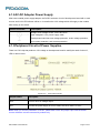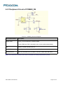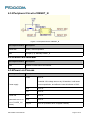
1
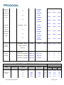
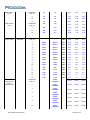
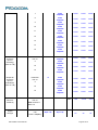
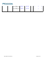
EVK-GT8619 User Manual Version:V1.0.2 Date:2015-08-24 1 Copyright Copyright ©2015 Fibocom Wireless Inc . All rights reserved. Without the prior written permission of the copyright holder, any company or individual is prohibited to excerpt, copy any part of or the entire document, or transmit the document in any form. Attention The document is subject to update from time to time owing to the product version upgrade or other reasons. Unless otherwise specified, the document only serves as the user guide. All the statements, information and suggestions contained in the document do not constitute any explicit or implicit guarantee. Trademark The trademark is registered and owned by Fibocom Wireless Inc. Versions Version Date Remarks V1.0.0 2013-07-30 Initial Version V1.0.1 2015-04-26 Update the description of copyright and attention. V1.0.2 2015-08-24 Update the logo. EVK-GT8619 User Manual Page 2 of 27 Applicability Type No. Type 1 G600 2 G610 Need adapter, ADP-G610-XXX-YY 3 G620 Need adapter, ADP-G620-XXX-YY 4 G510 Need adapter, ADP-G510-XXX-YY EVK-GT8619 User Manual Note Page 3 of 27 Contents 1 2 3 4 Preface...................................................................................................................................................................6 1.1 Scope.........................................................................................................................................................6 1.2 Audience................................................................................................................................................... 6 Overview................................................................................................................................................................7 2.1 Description................................................................................................................................................ 7 2.2 Specification............................................................................................................................................. 7 2.3 Development Board.................................................................................................................................8 Quick Guide.......................................................................................................................................................... 9 3.1 Connection................................................................................................................................................9 3.2 Run HyperTerminal or another Serial’s Tools on PC......................................................................... 9 3.3 Power Supply........................................................................................................................................... 9 Development Board Description..................................................................................................................... 10 4.1 Power Supply......................................................................................................................................... 10 4.1.1 Direct Power Supply..................................................................................................................... 10 4.1.2 AC-DC Adapter Power Supply.................................................................................................... 11 4.1.3 Peripheral Circuit of Power Supplies..........................................................................................11 4.2 Main Interfaced...................................................................................................................................... 12 4.2.1 Main DB9 RS232 Interface.......................................................................................................... 12 4.2.2 USB Interface.................................................................................................................................12 4.3 Switch and Control................................................................................................................................ 12 4.3.1 Peripheral Circuit of POWER_ON..............................................................................................13 4.3.2 Peripheral Circuit of RESET_N...................................................................................................14 4.3.3 LVDD LED Indicator...................................................................................................................... 14 4.3.4 Power on Process......................................................................................................................... 14 4.4 RTC (Real Time Clock).........................................................................................................................15 EVK-GT8619 User Manual Page 4 of 27 5 4.5 SIM Card Interface................................................................................................................................ 15 4.6 Audio Interface....................................................................................................................................... 15 4.7 ADC Interface.........................................................................................................................................16 4.8 Debugging Interface..............................................................................................................................16 Performance Testing......................................................................................................................................... 17 5.1 Current Testing.......................................................................................................................................17 5.2 Current Testing Description................................................................................................................. 18 5.3 RF Testing Description..........................................................................................................................21 6 RF Antenna.........................................................................................................................................................27 7 Default Jumped Cap......................................................................................................................................... 27 EVK-GT8619 User Manual Page 5 of 27 1 Preface 1.1 Scope This document outlines the evaluation kits of Fibocom module, related technical detail, and testing information about it. It ensures that the user can quickly and conveniently develop wireless communication products by themselves. 1.2 Audience The target audiences of this manual include engineers and testers who will use Fibocom module to develop wireless communication products. EVK-GT8619 User Manual Page 6 of 27 2 Overview 2.1 Description The GT8619 development kit can be used for testing Fibocom module after connecting to module via 50-pin connector. It has the following features: Each pin has a testing point Provides two methods to supply the power The main signal uses LED indicator Supports USB interface and RS232 serial port Support strace debugging software Two audio interfaces Supports SIM card interface Provides several buttons and jumper caps RF Cable included Supports SMA antenna interface 2.2 Specification Development board GT8619 DC power adapter AC 220V / DC 9V/1A Φ2.5mm Serial port line DB9 GSM antenna Frequency: 850/900/1800/1900MHz Impedance: 50ohm Gain: 0 dBi (unity) gain or greater VSWR: Less than: 2.5:1 EVK-GT8619 User Manual Page 7 of 27 2.3 Development Board Power Supply Switch BATT Voltage DC/DC Voltage Input Input Main RS232 Connector Reset Button Power on Button USB Connector SIM card Socket Antenna 1st Audio Data Logger Connector 2nd Audio Expanded RS232 Connector Figure 2- 1Development Board EVK-GT8619 User Manual Page 8 of 27 3 Quick Guide 3.1 Connection 1) Connect antenna transfer line to module RF interface 2) Install the modulator adapter on the development board 3) Install GSM antenna to SMA interface 4) Install SIM card 5) Ensure the installation of nine jumper capsJI2 6) Ensure the installation of jumper caps JP12, JM9 7) Ensure the installation of jumper caps JP11 (V40EXT---V33) 8) Ensure the installation of jumper caps JM5 (KEY---RESET_N) 9) Make sure the power supply switch is in the middle 10) Connect the PC serial port to EVB UART1by a serial port line 11) Plug in the power adapter 3.2 Run Hyper Terminal or another Serial’s Tools on PC 1) Open the corresponding serial port 2) Set the serial port of Hyper Terminal as 115200-8-N-1-None Flow 3.3 Power Supply 1) LV40 indicator is on when power adapter is plugged in 2) The switch is pushed to the direction of DC socket 3) LVDD indicator is on when the module is on 4) Press POWER_ON button for at least 600mS 5) LPG indicator and LCTS indicator are on if it successfully powered on. 6) Input AT command in PC Hyper Terminal, and return OK EVK-GT8619 User Manual Page 9 of 27 7) Input AT+ CSQ, and return +CSQ: 31,99 OK 8) The development board and the module works fine. Please refer to following chapters or AT Command User Manual. 4 Development Board Description This chapter introduces development board and corresponding functions of the module in details. 4.1 Power Supply Development board supports two kinds of power supplies. One can be directly connect with VBATT and supply power through connection end. The other supplies broader power through outside power supply. Development board switches the voltage to 4.0V through inside DC/DC, and then supplies power. 4.1.1Direct Power Supply Direct power supply will be loaded on modules. So the bound of power supply should refer to the requirement of GRPS module. Note: Please use correct voltage to avoid damage to the module. Power Connector Description DC power supply. V40BAT BATT = 3.3 V to 5.2 V GND 4.0V is recommended Supplied current > 2.0A Connect to 4V power Push Figure 4- 1 Direct Power Supply EVK-GT8619 User Manual Page 10 of 27 4.1.2AC-DC Adapter Power Supply After insert outside power supply adapter, the DC/DC set down circuit of development board will on work at once and LV40 LED indicator will be on. It transfers the 4.0V voltage which will supply to the module after turning on the switch. Power Connector Description Straight insert voltage socket, core is Φ2.5mm; Input voltage:8V~15V; power supply: ≥9W; Development board has over voltage protection, under voltage protection, over current protection, and reverse protection. 4.1.3Peripheral Circuit of Power Supplies There is a LDO chip that produces 3.3V voltage on development board to satisfy the need of other IC, LED or others circuit. Figure 4- 2 3.3V Power Circuit Jumper Switch Description JP12 Turn on/ off 3.3V voltage output JP11 Choose the power supply of LED or others circuit as VBATT or 3.3V Note: When you test the parameter of current, please take out the two jumper caps. And the tested current will be the current consumed by module only. EVK-GT8619 User Manual Page 11 of 27 4.2 Main Interface Main RS232 interface and USB interface use the same UART interface of the module. Six LED indicators(LRI/LDCD/LDSR/ DTR/LRTS/LCTS)can exactly indicate the logic level of each pin in UART interface of the module. The default value of main communication interface: adapt to baud rate -8-N-1-NONE. PC and other DTE equipments will fully satisfy all functions of the module through communication interface and AT command. Note: You cannot use two interfaces at the same time. Please switch between JI1 and JI2.You can identify whether is in SLEEP mode or not through the state of LCTS LED indicator. Jumper Switch Description JI1 Turn on/ off USB interface as main communication interface JI2 Turn on/ off Main RS232 as main communication interface 4.2.1Main DB9 RS232 Interface This interface is a complete 8-line interface, and it can be connected with PC or other DTE equipments directly. Development board has RS-232 Transceiver SP3238EEA inside. 4.2.2USB Interface Development board has USB transfer UART interface chip (PL2303). It will connect four interfaces (TXD/RXD/CTS/RTS) to UART interface of the module. LUSB LED indicator will be on after USB is inserted. Note: You need to install driver in some operating system when you use USB. 4.3 Switch and Control In this chapter, switch and control directions include: POWER_ON / RESET_N / LPG / TX_EN / VDD. LPG/TX_EN/VDD directs the state through LED indicator. POWER_ON / RESET_N have corresponding buttons and circuit. EVK-GT8619 User Manual Page 12 of 27 4.3.1Peripheral Circuit of POWER_ON Figure 4- 3 POWER_ON Circuit Diagram Development Board Description RM6 & CM11 Power_on pin is pulled up in GPRS module. Connect RM6 and CM11 externally to turn on the module automatically. JM7 Disable / Enable automatic turn-on KM2 & CM13 Manually turn on/off ensure it will excess 600mS UM5 and others When the automatic turn-on enable, it can be in effect even after reset. Note: The interval time should be more than 5s between the development board re-power. EVK-GT8619 User Manual Page 13 of 27 4.3.2Peripheral Circuit of RESET_N Figure 4- 4 Peripheral Circuit of RESET_N Development Board Description KM1&CM6 Button, manual reposition JM5 Jumper (1-3): Manually RESET_N 4.3.3LVDD LED Indicator Development Board Description JM9 Disable / Enable VDD LED indicator 4.3.4Power on Process Development Board Description LVDD Turn off If outside 3.3V voltage acts on any IO interface, it will cause current reperfusion, and affect the normal indicator of VDD. Power supply LPG Turn off LTX Turn off Power ON VDD Turn on (automatic turn on or LPG Turn on TX_EN Turn off (It twinkles when it register network) press POWER_ON button) EVK-GT8619 User Manual Page 14 of 27 Turn off Press POWER_ON button more than 3S, and the state of all LED is the same as power off mode. 4.4 RTC (Real Time Clock) The module includes a particular pin of RTC power supply. The RTC will continue running after main power supply is cut off. Lead the pin to JP7-1pin on development board, and design a 220uF standby capacitance. Short circuit JP7 (1-2pin) will ensure real time clock continue running about 160 seconds after the main power supply is cut off. You can directly provide power supply to KP7-1pin, or put a button battery to ensure the long-time running of real time clock. 4.5 SIM Card Interface Development board includes a complete SIM card socket and interface circuit. This circuit doesn’t support SIM_CD. 4.6 Audio Interface There are three audio interfaces: the first audio interface, the second audio interface and hand-free interface. As shown in the following picture: Figure 4- 5 Audio Interface EVK-GT8619 User Manual Page 15 of 27 The hand-free audio and the second audio interface are connecting to the same audio interface of the module, so you cannot use the second audio interface RJ11 and hand-free interface at the same time. Development Board JA3 Description JA3(1-2pin) Turn on/ off AUXO+ to hand-free interface JA3(3-4pin) Turn on/ off PA power supply hand-free interface JA3(5-6pin) Turn on/ off AUXO+ to hand-free interface 4.7 ADC Interface Development board JP7 (3pin/4pin)will connected to ADC1 and ADC2(80pin only). You can inquire about the voltage after ADC transfer through AT command. Note: Please remove RP10/RP11/RP12/RP13 when you test outside voltage. 4.8 Debugging Interface There is a debug interface inside development board. It will be used to analyze and debug the reference and function when the module is running. The interface will be simulated to UART through SPI, and then transferred to a serial port through RS-232 Transceiver SP3238EEA. Note: It just supports G600 and G610. Meanwhile there are LSINT/LSCS LED indicators on development board that will indicate the work state of SPI transfer serial port. Module SPI SC161S740 SP3238 Interface Figure 4- 6 SPI transfers to Serial Port Development Board Description JT1 Turn on/ off SPI transfer serial port circuit EVK-GT8619 User Manual Page 16 of 27 5 Performance Testing 5.1 Current Testing The current of the module is an important parameter. The development board is design with less current consumption. So it can be test with the module cooperatively. The current consumption reflected the G600 current consumption exactly. Here are the test procedures: 1) Use the direct power supply 2) Turn off 3.3V power supply(JM12) 3) Turn off outside power supply(JP11) 4) The main communication interface is USB interface, and provides UART interface voltage through VDD. 5) Turn off LVDD LED indicator 6) Turn off other interface connections The sketch map of testing environment: EVK-GT8619 User Manual Page 17 of 27 Figure 5- 1 Test Environment Note: It’s recommended that the power supply should be used Agilent 66311B or higher level programmable power supply. In this environment you don’t need a current meter. 5.2 Current Testing Description Example: G600 G600 Current Test Report Item STD- Uni G t 90.0 uA EGSM900 26.0 mA 24.5 DCS1800 26.0 mA 24.9 I idle-RX MAX 200.0 mA 135.7 I idle-base base (average) 23.0 mA 21.2 I off Description Condition Sample A RTC mode 75.0 GSM 900/1800 current I idle Idle mode EVK-GT8619 User Manual GSM only, DRX=2, -85dBm Page 18 of 27 I sleep Low power mode EGSM900, -85dBm DRX=2 4.0 mA 3.7 DRX=5 2.5 mA 2.3 DRX=9 2.0 mA 1.7 I sleep-RX MAX 200.0 mA 131.7 I sleep-base base (average) 1.3 mA 1.1 Average current EGSM900 PCL=5 300.0 mA 235.1 GSM voice PCL=10 160.0 mA 144.6 1 Tx slot PCL=15 130.0 mA 115.4 1 Rx slot PCL=19 125.0 mA 106.5 DCS1800 PCL=0 255.0 mA 186.7 PCL=5 155.0 mA 127.6 PCL=10 130.0 mA 108.0 PCL=15 125.0 mA 102.6 EGSM900 PCL=5 2000. mA 1060.1 I gsm-avg I gsm-max Peak current 0 GSM voice PCL=10 740.0 mA 476.9 1 Tx slot PCL=15 400.0 mA 291.4 1 Rx slot PCL=19 315.0 mA 241.1 DCS1800 PCL=0 1565. mA 740.8 0 PCL=5 630.0 mA 357.6 PCL=10 370.0 mA 229.3 PCL=15 315.0 mA 205.4 EGSM900 26.0 mA 24.6 DCS1800 26.0 mA 24.8 DRX=2 4.0 mA 3.6 GPRS 900/1800 current I idle I sleep Idle mode GPRS, DRX=2, -85dBm Low power mode EVK-GT8619 User Manual Page 19 of 27 I gprs-avg I gprs-max DRX=5 2.5 mA 2.2 DRX=9 2.0 mA 1.6 Average current EGSM900 PCL=5 520.0 mA 378.7 GPRS Class 10 PCL=10 260.0 mA 207.1 2 TX slot PCL=15 185.0 mA 149.5 3 Rx slot PCL=19 165.0 mA 134.3 DCS1800 PCL=0 420.0 mA 290.1 PCL=5 240.0 mA 177.0 PCL=10 180.0 mA 138.4 PCL=15 170.0 mA 126.5 EGSM900 PCL=5 2000. mA 1240.2 Peak current 0 GPRS Class 10 PCL=10 730.0 mA 575.9 2 TX slot PCL=15 400.0 mA 314.7 3 Rx slot PCL=19 315.0 mA 238.1 DCS1800 PCL=0 1565. mA 868.2 0 PCL=5 615.0 mA 429.5 PCL=10 360.0 mA 264.2 PCL=15 315.0 mA 202.0 Note: Test algorithm is not accurate, only for reference. Max Supply Current and Relative Power level recorded simultaneously Pay attention to the condition of GPRS attach It is the same Max Supply Current standard at GPRS or GSM EVK-GT8619 User Manual Page 20 of 27 5.3 RF Testing Description Example: G600 G600 RF Sector(EGSM900) Item Description Condition Test Report STD-ETSI Sample A STD-G Unit Channel 1 62 124 EGSM900 PCL=5 <90 <50 Hz -31.96 -10.33 19.89 Frequency 10 <90 <50 Hz -43.46 -9.75 -5.1 Error 15 <90 <50 Hz -24.67 -10.27 -8.78 19 <90 <50 Hz 13.62 -2.97 -7.88 RMS EGSM900 PCL=5 <5 <3 ° 0.6 1.0 0.9 Phase 10 <5 <3 ° 0.4 0.8 0.8 Error 15 <5 <3 ° 0.4 0.8 0.9 19 <5 <3 ° 0.8 0.8 0.8 Peak EGSM900 PCL=5 <20 <10 ° 5.7 6.0 4.7 Phase 10 <20 <10 ° -1.7 -2.3 -2.9 Error 15 <20 <10 ° 1.3 -2.2 -2.4 19 <20 <10 ° 2.1 -2.5 2.3 33±2 32.5±0.5 dBm 32.6 32.4 32.4 Transmitter ΔP≤1dB EGSM900 PCL=5 output 6 31±3 31±1.5 dBm 31.2 31.1 31.0 power 7 29±3 29±1.5 dBm 29.0 29.0 28.9 8 27±3 27±1.5 dBm 27.1 27.1 27.0 9 25±3 25±1.5 dBm 25.1 25.1 25.1 10 23±3 23±1.5 dBm 23.0 23.0 22.9 11 21±3 21±1.5 dBm 21.1 21.1 21.0 12 19±3 19±1.5 dBm 19.1 19.1 19.1 13 17±3 17±1.5 dBm 17.0 17.0 17.0 14 15±3 15±1.5 dBm 15.0 15.0 14.9 15 13±3 13±1.5 dBm 13.0 13.0 13.0 16 11±5 11±2.5 dBm 11.1 11.1 11.0 17 9 ±5 9 ±2.5 dBm 9.5 9.5 9.5 18 7 ±5 7 ±2.5 dBm 8.1 8.1 8.1 19 5 ±5 5 ±3 dBm 6.2 6.2 6.1 EVK-GT8619 User Manual Page 21 of 27 Transmitter EGSM900 PCL=5 output burst timing Template 6 (Pass or Fail) Insde Insde Template 7 Insde Template 8 Insde Template 9 Insde Template 10 Insde Template 11 Insde Template 12 Insde Template 13 Insde Template 14 Insde Template 15 Insde Template 16 Insde Template 17 Insde Template 18 Insde Template 19 Insde Template Output RF EVK-GT8619 User Manual EGSM900 PCL=5 Insde PASS PASS PASS PASS PASS PASS PASS PASS PASS PASS PASS PASS PASS PASS PASS PASS PASS PASS PASS PASS PASS PASS PASS PASS PASS PASS PASS PASS PASS PASS PASS PASS PASS PASS PASS PASS PASS PASS PASS PASS PASS PASS PASS PASS PASS PASS PASS PASS Page 22 of 27 spectrum Template (due to 10 Insde switching) Template (Pass or 15 Insde Fail) Template 19 Insde Template Output RF EGSM900 PCL=5 Insde spectrum Template (due to 10 Insde modulation) Template (Pass or 15 Insde Fail) Template 19 Insde Template EGSM900 PCL=5 Receiver ≤-102 ≤-108 dBm PASS PASS PASS PASS PASS PASS PASS PASS PASS PASS PASS PASS PASS PASS PASS PASS PASS PASS PASS PASS PASS PASS PASS PASS -109.00 -109.4 -109.2 BER<2.439% & sensitivity FER<1% EGSM900 Signal Cell Power=-88(dBm) 22(-3~+2) 22(-2~+2) 23 22 23 strength Cell Power=-102(dBm) 8(-4~+2) 8(-3~+2) 8 8 9 Cell Power=-108(dBm) 2(-4~+2) 2(-3~+2) 3 3 4 G600 RF Sector (DCS1800) Test Report Item Description Frequency Error EVK-GT8619 User Manual Condition STD-ETSI STD-G1 DCS1800 PCL=0 <180 <100 5 <180 10 15 Sample A Unit Channel 512 698 885 Hz -114.49 23.18 46.49 <100 Hz -13.56 -21.11 8.46 <180 <100 Hz 26.93 28.35 37.97 <180 <100 Hz 42.62 33.71 21.11 Page 23 of 27 RMS Phase Error Peak Phase Error Transmitter output power ΔP≤1dB Transmitter output burst timing (Pass or Fail) EVK-GT8619 User Manual DCS1800 PCL=0 <5 <3 5 <5 10 ° 0.91 0.96 1.04 <3 ° 1.03 0.82 0.82 <5 <3 ° 0.89 0.89 0.86 15 <5 <3 ° 0.84 0.88 0.97 DCS1800 PCL=0 <20 <10 ° 5.20 7.97 2.96 5 <20 <10 ° -3.64 2.61 2.90 10 <20 <10 ° 2.69 -2.61 2.85 15 <20 <10 ° 2.88 -2.74 -3.43 DCS1800 PCL=0 30±2 29.5±0.5 dBm 29.6 29.6 29.5 1 28±3 28±1.5 dBm 27.6 27.8 28.0 2 26±3 26±1.5 dBm 25.8 25.9 26.1 3 24±3 24±1.5 dBm 23.9 24.1 24.3 4 22±3 22±1.5 dBm 22.0 22.1 22.3 5 20±3 20±1.5 dBm 19.8 20.0 20.3 6 18±3 18±1.5 dBm 17.6 17.7 18.0 7 16±3 16±1.5 dBm 15.8 16.0 16.3 8 14±3 14±1.5 dBm 13.9 14.1 14.4 9 12±4 12±2 dBm 11.7 11.9 12.2 10 10±4 10±2 dBm 9.9 10.1 10.4 11 8±4 8±2 dBm 8.0 8.3 8.6 12 6 ±4 6 ±2 dBm 5.7 5.9 6.2 13 4 ±4 4 ±2 dBm 4.4 4.6 4.9 14 2 ±5 2 ±2.5 dBm 2.9 3.1 3.3 15 0 ±5 0 ±3 dBm 0.9 1.0 1.3 DCS1800 PCL=0 Insde Template PASS PASS PASS 1 Insde Template PASS PASS PASS 2 Insde Template PASS PASS PASS 3 Insde Template PASS PASS PASS 4 Insde Template PASS PASS PASS 5 Insde Template PASS PASS PASS 6 Insde Template PASS PASS PASS Page 24 of 27 Output RF spectrum (due to switching) (Pass or Fail) Output RF spectrum (due to modulation) (Pass or Fail) Receiver sensitivity Signal strength EVK-GT8619 User Manual 7 Insde Template PASS PASS PASS 8 Insde Template PASS PASS PASS 9 Insde Template PASS PASS PASS 10 Insde Template PASS PASS PASS 11 Insde Template PASS PASS PASS 12 Insde Template PASS PASS PASS 13 Insde Template PASS PASS PASS 14 Insde Template PASS PASS PASS 15 Insde Template PASS PASS PASS Insde Template PASS PASS PASS 5 Insde Template PASS PASS PASS 10 Insde Template PASS PASS PASS 15 Insde Template PASS PASS PASS Insde Template PASS PASS PASS 5 Insde Template PASS PASS PASS 10 Insde Template PASS PASS PASS 15 Insde Template PASS PASS PASS -109 -109.8 -108.5 22 22 22 DCS1800 PCL=0 DCS1800 PCL=0 DCS1800 PCL=0 *1 *2 ≤-100 ≤-107 22(-3~+2) 22(-2~+2) dBm BER<2.439% & FER<1% DCS1800 Cell Power=-88(dBm) Page 25 of 27 EVK-GT8619 User Manual Cell Power=-102(dBm) 8(-4~+2) 8(-3~+2) Cell Power=-107(dBm) 3(-4~+2) 3(-3~+2) 8 8 8 4 4 4 Page 26 of 27 6 RF Antenna There is SMA RF interface on development board. It is connected to RF interface of the module through a RF cable which transfers SMA to U.FL. The GSM antenna can be connected by the SMA connector. 7 Default Jumper Cap Figure 7- 1 Default Jumper Cap Number Locate PCS Description 1 JI2 9 Connect the Module UART to DB9 connector 2 JP12 1 Support the external voltage by LDO chip 3 JM5(1-3) 1 Support the external RESET button 4 JM9 1 Enable VDD led 5 JP11(1-2) 1 Support the external led voltage by VBAT 6 JT1 7 Connect the Module SPI as Trace port to DB9 connector EVK-GT8619 User Manual Page 27 of 27