1
co
m
APPLICATION NOTE
Application of the PCD3316
Caller Identification IC
ww
w.
yc
-d
z.
AN98071
Philips Semiconductors
Application of the PCD3316 Caller
Identification IC
Abstract
co
m
Application Note
AN98071
ww
w.
yc
-d
z.
This report describes the CMOS integrated circuit PCD3316 and offers the required application information for
designing the device in microprocessor controlled telephone sets and Adjunct Boxes with Caller-ID, Caller-ID on
Call Waiting and Caller-Name identification.
Purchase of Philips I2C components conveys a
license under the Philips I2C patent to use the
components in the I2C system, provided the system conforms to the I2C specifications defined by
Philips.
Philips Electronics N.V. 1998
All rights are reserved. Reproduction in whole or in part is prohibited without the prior written consent of the copyright owner.
The information presented in this document does not form part of any quotation or contract, is believed to be
accurate and reliable and may be changed without notice. No liability will be accepted by the publisher for any
consequence of its use. Publication thereof does not convey nor imply any license under patent- or other industrial or intellectual property rights.
2
Philips Semiconductors
Application of the PCD3316 Caller
Identification IC
Application Note
AN98071
co
m
APPLICATION NOTE
Application of the PCD3316
Caller Identification IC
z.
AN98071
-d
Author(s):
ww
w.
yc
Hans van Loon & Fred van Dongen
Philips Semiconductors Systems Laboratory Eindhoven,
The Netherlands
Keywords
CID / CIDCW
FSK
CAS
Bellcore approved
Add-on for telephone set
Number of pages: 69
Date: 98-08-26
3
Philips Semiconductors
Application of the PCD3316 Caller
Identification IC
Application Note
AN98071
Summary
ww
w.
yc
-d
z.
co
m
This report is intended to provide application support on system level (HW as well as SW), for designing
electronic telephone sets with the PCD3316 CIDCW receiver. The PCD3316 can be applied in ADSI phones,
feature phones and adjunct boxes with (Bellcore) CID, CIDCW and CNAM systems and in CTI systems with
VMWI.
The report explains the block diagram of the PCD3316 briefly and describes in more detail the functions of the
device. Considerations are given for handling of the input signals as CAS, FSK, ringing and polarity inversion.
Supply possibilities are discussed.
Ideas are offered for use of the device in different applications. A Bellcore approved telephone set with CID/
CIDCW and an application with VMWI, both built and tested, are described.
A chapter with ‘frequently asked questions and their answers’ is added.
The appendix gives an overview of the principles of signalling and requirements and standards.
4
Philips Semiconductors
Application of the PCD3316 Caller
Identification IC
Application Note
AN98071
CONTENTS
INTRODUCTION . . . . . . . . . . . . . . . . . . . . . . . . . . . . . . . . . . . . . . . . . . . . . . . 7
1.1
Definition and Abbreviations . . . . . . . . . . . . . . . . . . . . . . . . . . . . . . . . . . . . . 7
1.2
References . . . . . . . . . . . . . . . . . . . . . . . . . . . . . . . . . . . . . . . . . . . . . . 8
2.
PINNING AND BLOCK DIAGRAM. . . . . . . . . . . . . . . . . . . . . . . . . . . . . . . . . . . . . 10
3.
DESCRIPTION OF THE PCD3316 . . . . . . . . . . . . . . . . . . . . . . . . . . . . . . . . . . . . . 12
4.
APPLICATION CONSIDERATIONS . . . . . . . . . . . . . .
4.1
CAS receiving . . . . . . . . . . . . . . . . . . . . .
4.2
FSK receiving . . . . . . . . . . . . . . . . . . . . . .
4.3
Ring or Polarity Change Detection by POL0 and POL1
4.4
Power Down state . . . . . . . . . . . . . . . . . . .
4.5
Low Battery Detect . . . . . . . . . . . . . . . . . . .
4.6
Real-Time-Clock or Call-Timer signal . . . . . . . . .
.
.
.
.
.
.
.
.
.
.
.
.
.
.
.
.
.
.
.
.
.
.
.
.
.
.
.
.
.
.
.
.
.
.
.
.
.
.
.
.
.
.
.
.
.
.
.
.
.
.
.
.
.
.
.
.
.
.
.
.
.
.
.
.
.
.
.
.
.
.
.
.
.
.
.
.
.
.
.
.
.
.
.
.
.
.
.
.
.
.
.
.
.
.
.
.
.
.
.
.
.
.
.
.
.
.
.
.
.
.
.
.
.
.
.
.
.
.
.
.
.
.
.
.
.
.
.
.
.
.
.
.
.
.
.
.
.
.
.
.
.
.
.
.
.
.
.
.
.
.
.
.
.
.
17
17
20
25
31
31
31
5.
APPLICATION PROPOSALS . . . . . . . . .
5.1
Basic telephone set with CID / CIDCW .
5.2
Caller ID / Call Waiting Adjunct box . .
5.3
Application for British Telecom (BT) . .
5.4
Application for France Telecom (FT) . .
.
.
.
.
.
.
.
.
.
.
.
.
.
.
.
.
.
.
.
.
.
.
.
.
.
.
.
.
.
.
.
.
.
.
.
.
.
.
.
.
.
.
.
.
.
.
.
.
.
.
.
.
.
.
.
.
.
.
.
.
.
.
.
.
.
.
.
.
.
.
.
.
.
.
.
.
.
.
.
.
.
.
.
.
.
.
.
.
.
.
.
.
.
.
.
.
.
.
.
.
.
.
.
.
.
.
.
.
.
.
.
.
.
.
.
.
.
.
.
.
.
.
.
.
.
.
.
.
.
.
33
33
36
38
40
6.
REALIZED APPLICATIONS WITH THE PCD3316 . . .
6.1
Bellcore approved telephone set . . . . . . . . .
6.1.1
Hardware description . . . . . . . . .
6.1.2
Software description . . . . . . . . .
µC considerations. . . . . . . . . . .
6.1.3
6.1.4
Timing consideration . . . . . . . . .
6.1.5
Supply structure . . . . . . . . . . . .
6.1.6
POTS mode . . . . . . . . . . . . . .
6.1.7
What is done to get Bellcore approval
6.2
VMWI detector . . . . . . . . . . . . . . . . . .
6.2.1
Circuit description . . . . . . . . . . .
.
.
.
.
.
.
.
.
.
.
.
.
.
.
.
.
.
.
.
.
.
.
.
.
.
.
.
.
.
.
.
.
.
.
.
.
.
.
.
.
.
.
.
.
.
.
.
.
.
.
.
.
.
.
.
.
.
.
.
.
.
.
.
.
.
.
.
.
.
.
.
.
.
.
.
.
.
.
.
.
.
.
.
.
.
.
.
.
.
.
.
.
.
.
.
.
.
.
.
.
.
.
.
.
.
.
.
.
.
.
.
.
.
.
.
.
.
.
.
.
.
.
.
.
.
.
.
.
.
.
.
.
.
.
.
.
.
.
.
.
.
.
.
.
.
.
.
.
.
.
.
.
.
.
.
.
.
.
.
.
.
.
.
.
.
.
.
.
.
.
.
.
.
.
.
.
.
.
.
.
.
.
.
.
.
.
.
.
.
.
.
.
.
.
.
.
.
.
.
.
.
.
.
.
.
.
.
.
.
.
.
.
.
.
.
.
.
.
.
.
.
.
.
.
.
.
.
.
.
.
.
.
.
.
.
.
.
.
.
.
.
.
.
.
.
.
.
.
.
.
.
.
.
.
.
.
.
.
.
.
.
.
.
.
.
.
.
.
.
.
.
.
.
.
.
42
42
42
45
47
47
51
53
58
59
59
7.
FREQUENTLY ASKED QUESTIONS . . . . . . . . . . . . . . . . . . . . . . . . . . . . . . . . . . . 61
z.
co
m
1.
.
.
.
.
.
.
.
.
.
.
.
.
.
.
.
CID / SIGNALLING AND STANDARDS . . . . . . . . . . . . . . . . . . . . . . . . . . . 63
ww
APPENDIX 1
w.
yc
-d
.
.
.
.
.
Fig.1
Fig.2
Fig.3
Fig.4
Fig.5
Fig.6
Fig.7
Fig.8
Fig.9
Fig.10
Fig.11
Pin configuration . . . . . . . . . . . . . . . . . . . . . . . . .
Block diagram of the PCD3316 . . . . . . . . . . . . . . . . . .
Current consumption IDD versus VDD; operating and PD mode.
Signal path from line to CAS-input . . . . . . . . . . . . . . . .
Signal transfer from line to QR output and CASIN input . . . . .
Signal transfer from microphone to QR output and CASIN input .
CAS receive control procedure . . . . . . . . . . . . . . . . . .
FSK transmission specification (on-hook) . . . . . . . . . . . .
IRQ generation after reading a valid data byte . . . . . . . . . .
Signal path of FSK signals from line to FSK-inputs. . . . . . . .
Transfer from line to FSK inputs . . . . . . . . . . . . . . . . .
5
.
.
.
.
.
.
.
.
.
.
.
.
.
.
.
.
.
.
.
.
.
.
.
.
.
.
.
.
.
.
.
.
.
.
.
.
.
.
.
.
.
.
.
.
.
.
.
.
.
.
.
.
.
.
.
.
.
.
.
.
.
.
.
.
.
.
.
.
.
.
.
.
.
.
.
.
.
.
.
.
.
.
.
.
.
.
.
.
.
.
.
.
.
.
.
.
.
.
.
.
.
.
.
.
.
.
.
.
.
.
.
.
.
.
.
.
.
.
.
.
.
.
.
.
.
.
.
.
.
.
.
.
.
.
.
.
.
.
.
.
.
.
.
.
.
.
.
.
.
.
.
.
.
.
.
.
.
.
.
.
.
.
.
.
.
.
.
.
.
.
.
.
.
.
.
.
.
.
.
.
.
.
.
.
.
.
.
.
.
.
.
.
.
.
.
.
.
.
.
.
.
.
.
.
.
.
.
.
.
10
11
16
18
18
19
20
21
21
22
22
Philips Semiconductors
Application of the PCD3316 Caller
Identification IC
.
.
.
.
.
.
.
.
.
.
.
.
.
.
.
.
.
.
.
.
.
.
.
.
.
.
.
.
.
.
.
.
.
.
.
.
.
.
.
.
.
.
.
.
.
.
.
.
.
.
.
.
.
.
.
.
.
.
.
.
.
.
.
.
.
.
.
.
.
.
.
.
.
.
.
.
.
.
.
.
.
.
.
.
.
.
.
.
.
.
.
.
.
.
.
.
.
.
.
.
.
.
.
.
.
.
.
.
.
.
.
.
.
.
.
.
.
.
.
.
.
.
.
.
.
.
.
.
.
.
.
.
.
.
.
.
.
.
.
.
.
.
.
.
.
.
.
.
.
.
.
.
.
.
.
.
.
.
.
.
.
.
.
.
.
.
.
.
.
.
.
.
.
.
.
.
.
.
.
.
.
.
.
.
.
.
.
.
.
.
.
.
.
.
.
.
.
.
.
.
.
.
.
.
.
.
.
.
.
.
.
.
.
.
.
.
.
.
.
.
.
.
.
.
.
.
.
.
.
.
.
.
.
.
.
.
.
.
.
.
.
.
.
.
.
.
.
.
.
.
.
.
.
.
.
.
.
.
.
.
.
.
.
.
.
.
.
.
.
.
.
.
.
.
.
.
.
.
.
.
.
.
.
.
.
.
.
.
.
.
.
.
.
.
.
.
.
.
.
.
.
.
.
.
.
.
.
.
.
.
.
.
.
.
.
.
.
.
.
.
.
.
.
.
.
.
.
.
.
.
.
.
.
.
.
.
.
.
.
.
.
.
.
.
.
.
.
.
.
.
.
.
.
.
.
.
.
.
.
.
.
.
.
.
.
.
.
.
.
.
.
.
.
.
.
.
.
.
.
.
.
.
.
.
.
.
.
.
.
.
24
25
26
27
28
29
30
34
36
38
39
41
48
49
49
50
54
55
56
57
59
63
64
65
66
67
.
.
.
.
.
.
.
.
.
.
.
.
.
.
.
.
.
.
.
.
.
.
.
.
.
.
.
.
.
.
.
.
.
.
.
.
.
.
.
.
.
.
.
.
.
.
.
.
.
.
.
.
.
.
.
.
.
.
.
.
.
.
.
.
.
.
.
.
.
.
.
.
.
.
.
.
.
.
.
.
.
.
.
.
.
.
.
.
.
.
.
.
.
.
.
.
.
.
.
.
.
.
.
.
.
.
.
.
.
.
.
.
.
.
.
.
.
.
.
.
.
.
.
.
.
.
.
.
.
.
.
.
.
.
.
.
.
.
.
.
.
.
.
.
.
.
.
.
.
.
.
.
.
.
.
.
.
.
.
.
.
.
.
.
.
.
.
.
.
.
.
.
.
.
.
.
.
.
.
.
.
.
.
.
.
.
.
.
.
.
.
.
.
.
.
.
.
.
.
.
.
.
.
.
.
.
.
.
.
.
.
.
.
.
.
.
.
.
.
.
.
.
.
.
.
.
.
.
.
.
.
.
.
.
.
.
.
.
.
.
.
.
.
.
.
.
.
.
.
.
.
.
.
.
.
.
.
.
.
.
.
.
.
.
.
.
.
.
.
.
.
.
.
.
.
.
.
.
.
.
.
.
.
.
.
.
.
.
.
.
.
.
.
.
.
.
.
.
.
.
.
.
.
.
.
.
.
.
.
.
.
.
.
.
.
.
.
.
.
.
.
.
.
.
.
.
.
.
.
.
.
.
.
.
.
.
.
.
.
.
.
.
.
.
.
.
.
.
.
.
.
.
.
.
.
.
.
10
14
19
23
27
51
63
64
65
65
66
66
67
67
68
68
68
69
69
69
69
m
.
.
.
.
.
.
.
.
.
.
.
.
.
.
.
.
.
.
.
.
.
.
.
.
.
.
z.
-d
yc
Pin functions . . . . . . . . . . . . . . . . . . . . . . . .
Register contents . . . . . . . . . . . . . . . . . . . . . .
PCD3316 Mode register contents at CAS receive mode . .
PCD3316 Mode register contents at FSK receive mode . .
PCD3316 Mode register contents at POL detection mode .
Current consumption from VCC (line) and VDD (batteries)
CID characteristics . . . . . . . . . . . . . . . . . . . . .
CAS Characteristics . . . . . . . . . . . . . . . . . . . .
ACK Characteristics . . . . . . . . . . . . . . . . . . . .
CIDCW Timing Characteristics . . . . . . . . . . . . . . .
Single Data Message Format. . . . . . . . . . . . . . . .
SDMF 10 digit number delivery . . . . . . . . . . . . . . .
SDMF Private (“P”) / Out of Area (“O”) . . . . . . . . . . .
SDMF VMWI Message . . . . . . . . . . . . . . . . . . .
Multiple Data Message Format . . . . . . . . . . . . . . .
MDMF Date and Time . . . . . . . . . . . . . . . . . . .
MDMF 10 digit number delivery . . . . . . . . . . . . . .
MDMF 15 characters name delivery . . . . . . . . . . . .
MDMF Reason Absence CID . . . . . . . . . . . . . . . .
MDMF Reason Absence CNAM . . . . . . . . . . . . . .
MDMF VMWI Message . . . . . . . . . . . . . . . . . . .
ww
TABLE 1
TABLE 2
TABLE 3
TABLE 4
TABLE 5
TABLE 6
TABLE 7
TABLE 8
TABLE 9
TABLE 10
TABLE 11
TABLE 12
TABLE 13
TABLE 14
TABLE 15
TABLE 16
TABLE 17
TABLE 18
TABLE 19
TABLE 20
TABLE 21
.
.
.
.
.
.
.
.
.
.
.
.
.
.
.
.
.
.
.
.
.
.
.
.
.
.
co
FSK receive control procedure . . . . . . . . . . . . . . . . . . . .
POL0 and POL1 handling with a sinewave as input signal. . . . . .
Signal path of ringer signal from line to POL-inputs . . . . . . . . .
Transfer from line to POL inputs . . . . . . . . . . . . . . . . . . .
POL0/POL1 detection procedure . . . . . . . . . . . . . . . . . . .
Polarity change and ringer frequency detection procedure. . . . . .
Ringer frequency detection procedure. . . . . . . . . . . . . . . . .
Block diagram of basic telephone set with CID/CIDCW functions . .
Block diagram of an Adjunct box . . . . . . . . . . . . . . . . . . .
BT application; Down stream signalling and timing of control signals
BT application; circuit adaption to basic set of Fig.19 . . . . . . . .
FT application; CID signalling and timing of control signals . . . . .
Normal CIDCW signal handling. . . . . . . . . . . . . . . . . . . .
The CAS signal is not followed by FSK message. . . . . . . . . . .
FSK and IRQ timing (complete signals). . . . . . . . . . . . . . . .
Detailed FSK and IRQ timing. . . . . . . . . . . . . . . . . . . . .
Line interrupter and ringer circuit . . . . . . . . . . . . . . . . . . .
Transmission and dialler circuit . . . . . . . . . . . . . . . . . . . .
PCD3316 configuration . . . . . . . . . . . . . . . . . . . . . . . .
Display part . . . . . . . . . . . . . . . . . . . . . . . . . . . . . .
VMWI detector circuitry . . . . . . . . . . . . . . . . . . . . . . . .
CID Timing . . . . . . . . . . . . . . . . . . . . . . . . . . . . . .
CIDCW Protocol . . . . . . . . . . . . . . . . . . . . . . . . . . .
CIDCW order . . . . . . . . . . . . . . . . . . . . . . . . . . . . .
Single Data Message Format. . . . . . . . . . . . . . . . . . . . .
Multiple Data Message Format . . . . . . . . . . . . . . . . . . . .
w.
Fig.12
Fig.13
Fig.14
Fig.15
Fig.16
Fig.17
Fig.18
Fig.19
Fig.20
Fig.21
Fig.22
Fig.23
Fig.24
Fig.25
Fig.26
Fig.27
Fig.28
Fig.29
Fig.30
Fig.31
Fig.32
Fig.33
Fig.34
Fig.35
Fig.36
Fig.37
Application Note
AN98071
6
.
.
.
.
.
.
.
.
.
.
.
.
.
.
.
.
.
.
.
.
.
.
.
.
.
.
.
.
.
.
.
.
.
.
.
.
.
.
.
.
.
.
.
.
.
.
.
.
.
.
.
.
.
.
.
.
.
.
.
.
.
.
.
Philips Semiconductors
Application of the PCD3316 Caller
Identification IC
1.
Application Note
AN98071
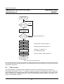
INTRODUCTION
m
The PCD3316 is a CMOS integrated circuit for receiving physical layer signals like Bellcore’s CPE Alerting Signal
(CAS) and BT’s Idle State Tone Alert Signal. The device is capable of a very high precision detection of the dual
tone (2130 and 2750 Hz) by using a patented digital algorithm.
co
For timing purposes the PCD3316 can be programmed to generate an interrupt signal to the micro-controller
every second or every minute. This can be used for Real-Time-Clock and timing purposes, these timings are
derived from an on chip 32.768 kHz crystal oscillator.
Also incorporated in the device are an FSK receiver/demodulator and a Ring or Polarity Change detector.
z.
The status of the PCD3316, the received FSK data bytes and the ringer period can be read, from internal
register, and many options can be selected via the I2C-bus serial interface.
Detection of a polarity change on the inputs POL0 or POL1, the reception of an FSK data byte, the detection of a
CAS tone or a time base interrupt is signalled to the micro-controller by an interrupt request signal (IRQ). In
power-down mode only the polarity comparators and the 32.768 kHz oscillator are active. The micro-controller
can communicate with the PCD3316 device via the serial interface.
-d
The PCD3316 can be used in Analog Display Services Interface (ADSI), feature phones and adjunct boxes with
Bellcore CID (Caller-ID), CIDCW (Caller-ID on Call Waiting) and CNAM (Caller-NAMe) systems and Computer
Telephony Integrated (CTI) systems.
Caller ID was first developed in the Bell labs, after which Nortel made the first practical implementation.
Nowadays there are two FSK (Frequency Shift Keying) standards Bell 202 and CCITT V23, which mainly differ in
the actual bits frequency (Bell is 1200 Hz and 2200 Hz, while CCITT is 1100 Hz and 2100 Hz). The basic Caller
ID types ‘Caller ID type 1 and type 2’, supported by the PCD3316, are specified in APPENDIX 1.
Definition and Abbreviations
a/b; b/a
ADSI
AGC
AP
BRL
BT
BOM
BOM
CAS
CID
CIDCW
CNAM
CND
CPE
Cradle
CTI
DEMO
DMO
DTMF
EMC
Line terminals of application
Analog Display Service Interface
Automatic Gain Control; line loss compensation facility
Access Pause
Balance Return Loss
British Telecom
Begin Of Mark (FSK transmission)
Bill Of Materials (Components List)
CPE Alerting System
Caller Identification Delivery
Caller Identification Delivery on Call Waiting
Caller NAMe delivery
Caller Number Delivery
Customer Premises Equipment
Hook key
Computer Telephony Integrated systems
Demonstration model
Dial Mode Operation
Dual Tone Multi Frequency
Electro Magnetic Compatibility
ww
w.
1.1
yc
The PCD3316 is designed with differential FSK inputs and a separated single ended CAS input to guarantee
reception of low level signals respectively to separate CAS tones from near end speech by means of the side
tone circuitry of the applied transmission IC.
7
Philips Semiconductors
Application of the PCD3316 Caller
Identification IC
yc
-d
z.
co
m
Frequency Shift Keying
France Telecom
Hardware
Line current into the a/b-terminals
Inter-Integrated Circuit bus
Idle State Alert Signal
Light Crystal Display
Liquid Emitting Diode
Display module with driver PCF2116K
Last Number Redial
Multiple Data Message Format
Microphone input
Non-Disclosure Agreement
Handset is lifted (Switch “cradle” in position OFF)
Handset is on the base (Switch “cradle” in position ON)
Demo Board with the UBA1702, TEA1112, PCD3755F, PCD3316 and LPH7319-3
One Time Programmable Read Only Memory
Sound pressure in Pascal; 1 Pa = 1 N/m2 = 94 dBSPL
Printed Circuit Board
Caller-ID and caller ID on Call Waiting receiver
OTP microcontroller
Power On Reset
Plain Old Telephone Services
Recall
Subscriber Alerting Signal
Signal Noise and Distortion ratio
Single Message Data Format
Software
Tone Alert Signal
Transmission IC
Positive Earpiece input
Negative Earpiece input
Line interrupter driver and ringer for PMOST
Line interrupter driver and ringer for PNP
Reference voltage of PCD3316, 1.25 V typical
Power-on reset hysteresis voltage, 100 mV typical
Power-on reset high voltage, 2.05 V typical
Visual Message Waiting Indicator
Input impedance with respect to AGND
Line impedance
Set impedance between the a/b-terminals
ww
w.
FSK
FT
HW
Iline
I2 C
ISAS
LCD
LED
LPH7319-3
LNR
MDMF
MIC
NDA
Off-hook
On-hook
OM5843
OTP
Pa
PCB
PCD3316
PCD3755F
POR
POTS
RCL
SAS
SINAD
SMDF
SW
TAS
TEA1112
TEL+
TELUBA1702
UBA1702A
Vref
Vhys(POR)
VPOR(H)
VMWI
Zi
Zline
Zset
Application Note
AN98071
1.2
References
[1]
Philips Semiconductors DATA sheet ‘PCD3316 CIDCW receiver’ product specification May 1998. Order
number: 9397 750 03525.
[2]
Philips Semiconductors User Manual OM5843 Report No.: ETT/UM97002.4, ‘PCD3316 CID/CW demo
board’, from 97-11-24.
[3]
Philips Semiconductors Data Handbook IC03a, ‘Semiconductors for Wired Telecom Systems’, 1997. Order
no. 9397 750 00839
8
Philips Semiconductors
Application of the PCD3316 Caller
Identification IC
Application Note
AN98071
Philips Semiconductors Application Handbook IC03b, ‘Semiconductors for Wired Telecom Systems’, 1997.
Order no. 9397 750 00811
[5]
Philips Semiconductors I2C Peripherals Data Handbook IC12, order number: 9398 750 01647, or the
Brochure ‘The I2C-bus and how to use it’, order no. 9398 393 40011.
[6]
TIA/EIA PN-3647 (to become ANSI TIA/EIA-xxx-1997) ‘Telecommunications Telephone Terminal
Equipment Type 1 Caller Identity Equipment Performance Requirements’, from july 1997.
Publication from: Telecommunication Industry Association, Engineering Department, Suite 300, 2500
Wilson Boulevard, Arlington, VA22201.
[7]
prETS 300 778-1 (draft) ‘PSTN; Protocol over the local loop for display and related services; Terminal
Equipment requirements; Part 1: Off-line (on-hook) data transmission’, from june 1997.
Publication from ETSI: European Telecommunications Standard Institute
[8]
ETS 300 659-1 ‘PSTN; Subscriber line protocol over the local loop for display and (related services); Part 1:
On-hook data transmission’, from february 1997.
Publication from ETSI: European Telecommunications Standard Institute
[9]
Philips Semiconductors Application Note AN96045. “Reference specification of a dialler implementing the
reference design”, Authors: C.D.Holzscherer, R.J.Cornelissen, J.G.K.Fajta. Date 16 October 96
-d
z.
co
m
[4]
[10] LSSGR: Voiceband Data Transmission Interface Section 6.6, Generic Requirements GR-30-CORE issue 1,
December 1994, Bell Communications Research (Bellcore).
[11] CPE Compatibility Considerations for the Voiceband Data Transmission Interface, Special Report SR-TSV002476 issue 1, December 1992, Bell Communications Research (Bellcore).
yc
[12] BT, SIN 242 Issue 02, Nov 1996. ‘Calling line identification service. Terminal Equipment Requirements
Part1 Idle state, Down stream signalling, Part 2 Loop state signalling
ww
w.
[13] France Telecom Recommandation B 14-10W 1995, ‘Interface de reception de l’identite du demandeur et de
la notification pour terminaux analogiques’, Edition 1 de septembre 1995.
9
Philips Semiconductors
Application of the PCD3316 Caller
Identification IC
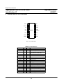
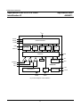
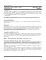
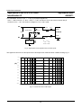
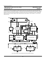
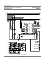
PINNING AND BLOCK DIAGRAM
co
m
2.
Application Note
AN98071
handbook, halfpage
HXIN 1
16 VDD
HXOUT 2
15 FSKIN+
IRQ 3
14 FSKIN−
13 CASIN
z.
SCL 4
PCD3316
SDA 5
12 LOWBAT
LXIN 6
11 POL0
LXOUT 7
10 POL1
9 AGND
-d
DGND 8
MBH980
yc
Fig.1 Pin configuration
SYMBOL
TABLE 1 Pin functions
PIN
I/O DESCRIPTION
1
I
3.58 MHz crystal oscillator input
HXOUT
2
O
3.58 MHz crystal oscillator output
IRQ
3
O
interrupt output; programmable
active HIGH or active LOW
w.
HXIN
SCL
4
I
serial clock line of I2C-bus
SDA
5
I/O
serial data line of I2C-bus
6
I
32.768 kHz crystal oscillator input
7
O
32.768 kHz crystal oscillator output
DGND
8
−
digital ground
AGND
9
−
analog ground
POL1
10
I
polarity detector input 1
POL0
11
I
polarity detector input 0
LOWBAT
12
I
low battery detector input
CASIN
13
I
input pin for CAS signal
FSKIN−
14
I
negative input for FSK signal
ww
LXIN
LXOUT
FSKIN+
15
I
positive input for FSK signal
VDD
16
−
positive supply
10
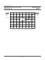
Philips Semiconductors
Application of the PCD3316 Caller
Identification IC
co
m
Application Note
AN98071
VDD
agewidth
16
CASIN
HXIN
HXOUT
14
z.
FSKIN−
PREPROCESSOR
13
1
2
3.58 MHz
OSCILLATOR
LEVEL
DETECT
TIMING
CAS
FSK
-d
FSKIN+
15
3
LOWBAT
POL0
POL1
12
11
10
yc
CONTROL
VOLTAGE
REFERENCE
w.
4
I2C-BUS
INTERFACE
POR
8
5
6
TIME
BASE
32.768 kHz
OSCILLATOR
7
MBH983
AGND
ww
Fig.2 Block diagram of the PCD3316
11
SCL
SDA
PCD3316
9
DGND
IRQ
LXIN
LXOUT
Philips Semiconductors
Application of the PCD3316 Caller
Identification IC
3.
Application Note
AN98071
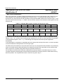
DESCRIPTION OF THE PCD3316
m
A brief description of the PCD3316 is given in this chapter with reference to block diagram Fig.2. Evaluation
results are presented of some of the PCD3316 blocks which are derived from a typical sample measured at room
temperature.
co
VDD = 3.0 V; values of input impedances are given as typical values; unless otherwise written. The dBm values
are referred to 0 dBm = 775 mVrms. The pinning and the pin functions of the PCD3316 are shown in Fig.1
respectively in TABLE 1.
z.
An overview of the registers is given in the ‘CONTROL’ block by means of TABLE 2. Consult the PCD3316 data
sheet [1] for circuit details, detailed description of the registers and characteristics.
PRE-PROCESSOR (FSKIN+, FSKIN−, CASIN)
-d
The FSK or CAS signals from the telephone line are processed by the pre-processor block by means of an A/D
converter and a digital bandpass filter. The bandpass filter is applied for FSK or CAS signals depending on the
mode selection in Mode register 1.
The inputs FSKIN+ and FSKIN− have a differential Zi of 1.4 MΩ. The single ended CASIN input measures
1.4 MΩ to AGND. The pre-processed signals are delivered to the Level detector, CAS detector and FSK
receiver.
The CAS detector will be enabled (FSK receiver disabled):
- In Off-hook (speech) mode
yc
The FSK receiver will be enabled (CAS detector disabled):
- In CID / on-hook mode after detection of a ringing signal
- After detection of a correct CAS tone in BT mode (on-hook) or CIDCW in off-hook mode
Harmonics of pre-processed FSK / CAS signals:
- FSK: The harmonics of the output signal of the pre-processor are below the −69 dBm at an input signal of
0 dBm signal, 1951 Hz and up to a frequency range of 8 kHz.
w.
- CAS: The harmonics of the output signal of the pre-processor are below the −62 dBm at an input signal of
0 dBm signal, 1078 Hz and up to a frequency range of 8 kHz.
The CASIN input is a single ended input. More noise and distortion is expected from the reference voltage in
comparison with the differential FSK input.
To prevent a so called ‘Talk-Off’, the first harmonic has to be low with respect to the input sensitivity from 0
dBm till around −38 dBm. Lower input levels will not be treated as valid signals. The first harmonic in worst
case is around −55 dBm which is far below the requirements.
ww
The noise level is about −80 dBm and constant over the over the frequency band from 300 Hz to 8 kHz.
3.58 MHz OSCILLATOR (HXIN, HXOUT)
The 3.58 MHz oscillator has to be activated by means of an external quartz crystal or ceramic resonator
connected between the HXIN and HXOUT pins. This oscillator is needed for the FSK receiver and CAS detection
and must be switched-off in power down mode by register setting; see [1].
TIMING
The block delivers the timing signals, generated by the 3.58 MHz oscillator, to the control block.
12
Philips Semiconductors
Application of the PCD3316 Caller
Identification IC
Application Note
AN98071
LEVEL DETECT
co
m
The level detector has a threshold of − 40 dBm typical. When the average signal level on FSKIN+/− ‘or’ CASIN is
below this threshold, within a time period of about 8 ms, the LOW Level bit is set (Interrupt status register). The
level detector is used to observe a carrier loss during FSK transmission and to detect the TAS signal for BT.
CAS
z.
After a Power-on reset or enabling the CAS detector the internal CAS registers are initialized. When a correct
dual tone of 2130 Hz and 2750 Hz is detected with a duration of more than 60 ms, while the CAS detector is
enabled, the PCD3316 will generate an interrupt and the CAS Interrupt is set (Interrupt register). Generation of
interrupts will be blocked when the signal level on the CASIN input is below the threshold of the level detector.
FSK
-d
The FSK receiver can be enabled by setting the FSK on/off bit (Mode register 1). FSK transmission protocol
starts with a channel seizure (alternation of 0’s and 1’s) followed by a block of marks (only 1’s) and finally by the
FSK data word (ref: BT / Bellcore specs) which consists of a start bit, eight data bits and a stop bit. After detection
of the mark bits, the FSK-BOM indication bit is set (Status register). The FSK receiver generates an interrupt
after receiving the complete data word at the IRQ pin. When a valid data word has been received, the FSK data
is available in the FSK data register for further processing by the microcontroller.
CONTROL (IRQ)
yc
This block takes care of the IRQ (Interrupt ReQuest) handling and the interface control of internal registers, I2C
interface and low battery, polarity, FSK and CAS detection.
The IRQ push-pull output is evaluated at VDD = 3.0 V with respect to maximum PORT current in low as well as in
high state. Also, the output levels are measured at 2 mA source and sink currents.
Input current (low state) = 5.4 mA when 0.4 V is applied on IRQ
Output current (high state) = 7.5 mA when 2.6 V is applied on IRQ
w.
Low level = 0.14 V when 2 mA is forced into IRQ
High level = 2.90 V when 2 mA is drawn out of IRQ
Low battery detection (LOWBAT)
ww
A tap of the battery voltage can be compared with Vref by means of the LOWBAT input. If the level on LOWBAT
is less than Vref, indicating end of battery life-time, the LOW-BAT indication (Status register) is set. The LOWBAT indication is cleared when the level on LOWBAT is more than Vref.
Ring or Polarity change detector (POL0, POL1)
Two comparators are available for ring and polarity detection. The ringing signal and polarity change of the DC
line voltage are received by the inputs POL0 and POL1, via input attenuators, and compared with Vref from the
Voltage reference block. A POL0 or POL1 interrupt is generated when the level on input POL0 or POL1 crosses
the Vref reference level.
A polarity reversal is detected when a POL1 or POL0 interrupt is generated without setting the ringer period
register. A ringer signal is detected when a sequence of interrupts are generated from POL1-POL0-POL1...
which sets the ringer period register with the period time of the ringer signal by means of a binary value.
13
Philips Semiconductors
Application of the PCD3316 Caller
Identification IC
Application Note
AN98071
Registers
m
The PCD3316 has in total six internal registers, four registers are read only and contain the internal status/
interrupt and counter values, the two last registers are read/write and control the functionality of the device. In
TABLE 2 these registers with there contents are given, for a detailed description see reference [1].
BIT 7
co
.
TABLE 2 Register contents
BIT 5
BIT 4
BIT 3
BIT 6
Interrupt status register CIDINT; address 00H; read only
SEC interrupt
FSK
interrupt
Low Level
Status
FSK data register CIDFSK; address 01H; read only
D7
D6
D5
D4
Status register CIDSTA; address 02H; read only
POL1
LOW-BAT
Indication
POL0
POL1
Interrupt
BIT 1
BIT 0
POL0
Interrupt
CAS
Interrupt
RES
z.
MIN
Interrupt
BIT 2
FSK-BOM
Indication
D3
D2
D1
D0
FSK-OVR
Error
FSK-FRM
Error
RES
RES
D3
D2
D1
D0
INT Polarity
HIGH/LOW
RES
RES
RES
RES
RES
D7
D6
-d
Ringer period register CIDRNG; address 03H; read only
D5
D4
Mode register 1 CIDMD1; address 04H; read/write
FSK
on/off
FSK BOM-mask
on/off
CAS on/off
POL on/off
Mode register 2 CIDMD2; address 05H; read/write
POR
TB on/off
SEC/MIN
INT-SUP
on/off
yc
XTAL
on/off
VERSION 1 VERSION 0
w.
An on-chip Power-On Reset circuit activates a reset as long as VDD is below VPOR(H). If VDD exceeds this level,
the 3.58 MHz oscillator starts to initiate the PCD3316 and to set the registers to their default value. The
initialization takes a maximum of 100 clock-cycles. The performance of the IC will be reached at the specified
minimum supply voltage of 2.5 V. The IC will be switched-off when a falling VDD crosses the threshold
VPOR(H) − Vhys(POR).
Measured levels are: VPOR(H) = 1.99 V, VPOR(L) = 1.88 V, Vhys(POR) = 110 mV.
ww
I2C - BUS INTERFACE (SCL, SDA)
The I2C-bus interface takes care of the communication with the microcontroller which is required in a system with
the PCD3316. The IC operates in the slave transmitter/receiver mode only. The I2C-bus is for bidirectional, twoline communication between different ICs or modules via the serial data line (SDA) and the serial clock line
(SCL).
The status of the PCD3316, the received FSK data and the ringer period can be read while many options can be
selected via the I2C-bus.
Both lines have to be connected to VDD via pull-up resistors. A detailed description of the I2C-bus specification
can be found in [5].
14
Philips Semiconductors
Application of the PCD3316 Caller
Identification IC
Application Note
AN98071
Input levels
co
m
SDA and SCL are the only two digital inputs of the device. Both pins are identical I/O’s with the difference that the
output path of pin SCL is disabled. The input levels of these I2C pins are specified between 0V and 30% of VDD
for low levels and between 70% of VDD and VDD for high levels. Test results show low levels between 0V and
> 33% of VDD and high levels between < 63% of VDD and VDD.
Output currents
The SDA output (open drain) can drive only a logical ’0’. For values of the output current in low state refer to
‘Control (IRQ)’ in this chapter, because the circuitry for driving the low levels are in both ports the same.
z.
VOLTAGE REFERENCE
This block generates the reference voltage Vref = 1.25 V (±100 mV) applied for low battery detection and ring or
polarity detection.
TIME BASE
-d
The time base block is driven by the 32 kHz oscillator. In case the TB-on/off bit (Mode register 2) is set, the time
base block generates a 1 second or a 1 minute interrupt signal and every second or minute the MIN and/or SEC
interrupt bits are set. The SEC/MIN bit (Mode register 2) selects whether every second or every minute an
interrupt is generated. All possible selections can be found in [1].
Resetting bit TB on/off will only disable the time base interrupts; the 32 kHz oscillator continues to operate.
yc
32 kHz OSCILLATOR (LXIN, LXOUT)
This oscillator is permanently operating. It uses a 32.768 kHz quartz crystal (or resonator) connected between
the LXIN and LXOUT pins. The 32 kHz oscillator is used for the Ring or Polarity change detector, the Low battery
detector, the Low level detector, detection of a correct twist level and for generation of either 1 second or 1
minute interrupt.
w.
SUPPLY / Ground references / Power down (VDD, DGND, AGND)
ww
This part which is not indicated in the block diagram requires some explanation.
The PCD3316 is supplied via the VDD pin; the VDD voltage has to be between 2.5 V and 3.6 V. The device has
two ground references, DGND is the ground reference of the digital circuitry of the PCD3316 while AGND is the
reference ground of the analog inputs POL0, POL1, LOWBAT, FSKIN+, FSKIN- and CASIN. The ground
references have to be star-connected to the supply ground on the PCB to prevents disturbances of the analog
ground.
The specified current consumption is 2.3 mA maximum in operating mode and 70 µA maximum in power down
mode at VDD = 2.5 V in both cases.
The current consumption IDD as a function of VDD of the PCD3316 is shown in Fig.3 for operating as well as PD
mode. In operating mode both clocks are running, 3.58 MHz and 32 kHz, while FSK as well as CAS are disabled.
The 3.58 MHz clock is disabled in PD mode. In this mode only the POL/LOWBAT-comparators and the 32 kHz
oscillator are active. The internal ‘power down’ is SW-controlled.
15
Philips Semiconductors
Application of the PCD3316 Caller
Identification IC
(LIN)
(LIN)
100.0
m
3.0
Application Note
AN98071
power down
operating
IDD
2.6
(mA)
2.4
90.0
operating
2.2
co
2.8
80.0
IDD
70.0
(µA)
60.0
power down
z.
2.0
1.8
1.6
1.2
2.0
2.4
2.2
-d
1.4
2.8
2.6
3.0
40.0
30.0
20.0
10.0
3.2
3.6
3.4
ww
w.
yc
Fig.3 Current consumption IDD versus VDD; operating and PD mode
16
50.0
VDD (V)
Philips Semiconductors
Application of the PCD3316 Caller
Identification IC
4.
Application Note
AN98071
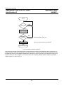
APPLICATION CONSIDERATIONS
4.1
co
m
For receiving CAS, FSK and POLs signals special hardware and control (software) are necessary while
recognizing the difference between polarity inversion and ringing needs special control. In all these cases also
the connection with a micro-computer and the supply considerations e.g mains, batteries and/or telephone line
supply are important. This chapter gives considerations on these hardware and control (software).
CAS receiving
The Bellcore’s CAS (CPE Alerting System) signals are only received in off-hook mode, if the CAS detection is
enabled. The PCD3316 will generate an interrupt when a correct dual tone (2130 and 2750 Hz) is detected. After
receiving a proper CAS signal the PCD3316 will be switched to FSK mode and waits for CIDCW messages.
z.
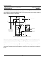
Hardware considerations:
CAS tones with frequencies of 2130 Hz and 2750 Hz have to be detected in off-hook mode by the PCD3316 at
signal levels down to −32 dBm on the line (Bellcore spec). To reduce the influence from near end speech, the
CASIN input of the PCD3316 is coupled to the receive output (QR) of the transmission IC, taking advance of the
side tone suppression of the transmission circuitry. Furthermore, a high pass filter in the CAS signal transfer
(CAS-HP) reduces also the influence of speech.
yc
-d
The input sensitivity of the PCD3316 is −37.8 dBm minimum. So, the CAS tones (at 2130 Hz and 2750 Hz) can
be attenuated from line to CASIN input, taking into account the:
- required gain of the receiver stage of the transmission IC which depends on the sensitivity of the earpiece
and the loudness requirements of the set
- influence of the CAS-HP filter at the CAS tone frequencies
- influence of the low pass filter of the receiver stage (receive-LP) of the transmission IC depending on the
loudness requirements of the set
w.
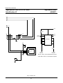
The signal path of the CAS tones from line to CASIN input of the PCD3316 is shown in Fig.4. The components
from receiver output of the transmission IC corresponds with the components of the application of chapter 6.1.
The CAS signal from the line is attenuated by the anti side-tone network, amplified by the receiver stage of the
transmission IC, filtered by the ‘receive-LP’ filter and the ‘CAS-HP’ filter before it is offered to the CASIN input.
The resistor in series with the earpiece can be necessary to attenuate the signal to the earpiece while a larger
gain is required for the CAS tones.
The cut-off frequency f-LP of the ‘receive-LP’ filter is determined by C117 and R119//Rint; Rint is an internal
resistance of the transmission IC. The cut-off frequency f-HP of the ‘CAS-HP’ filter is determined by C1cas and
Rcas//ZiCAS with ZiCAS is the input impedance of the CASIN input. Capacitor C2cas is a couple device determined
by: C2cas . ZiCAS >> C1cas . Rcas.
ww
The application of chapter 6.1 (Bellcore approved) is taken as an example.
Receive gain: The overall gain from line to earpiece is −10 dB due to the application of a sensitive earpiece. This
−10 dB attenuation is too much for the CAS tones. The lowest signal levels at the line of −32 dBm can not be
detected by the PCD3316 because they are below the −40 dBm threshold. In this case the receive gain is
enlarged for the CAS tones and reduced for the earpiece by the series resistor Rs. The gain from line to CASIN
input is adjusted to −4 dB (by means of R119 = 330 kΩ) while the gain from line to earpiece is −10 dB due to Rs
= 100 Ω and the internal resistance of the Mute-switch. The applied earpiece has an impedance of 150 Ω.
CAS tone transfer: Due to the effect of the ‘receive-LP’ and the ‘CAS-HP’ filters at the CAS tone frequencies on
the adjusted gain, the resulting attenuation of the CAS tones is about −6 dB (instead of the adjusted −4 dB) as
shown in Fig.5. The cut-off frequency is chosen at f-HP = 800 Hz with C1cas = 1.8 nF and Rcas = 120 kΩ while
ZiCAS = 1.4 MΩ typical.
17
Philips Semiconductors
Application of the PCD3316 Caller
Identification IC
Application Note
AN98071
m
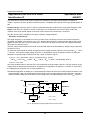
Cut-off frequency f-LP is set at 7.5 kHz with C117 = 270 pF, R119 = 330 kΩ and Rint = 100 kΩ as a result of
acoustical tests.
+
vline
b/a
Z-set
VCC
transmission IC
attenuator
filters
MIC
MIC
GAR
(TEA111X)
mic
IR
SLPE
VEE
CAS-HP
C1cas
R119
C2cas
Rcas
C117
CASIN
PCD3316
Rs
Mute
switch
-d
anti side-tone network
QR
receive-LP
z.
LN
Vph
co
a/b
Fig.4 Signal path from line to CAS-input
(LIN)
yc
0.0
-2.0
[dB]
vline = − 10 dBm
QR output
-4.0
from line to:
w.
-6.0
CASIN input
-8.0
-10.0
ww
-12.0
-14.0
-16.0
300.0
freq. [Hz]
1.0k
10.0k
A l i AC
Fig.5 Signal transfer from line to QR output and CASIN input
Near end speech: Own speech can influence the detection of CAS tones because the levels of speech at the
line can be more than the lowest CAS tone levels. The anti side-tone network of the transmission IC reduces
the transfer of own speech from microphone to earpiece, and CASIN input in this case. The reduction depends
on the line termination and the definition of the anti side-tone network; consult the ‘side tone stories’ in [3].
18
Philips Semiconductors
Application of the PCD3316 Caller
Identification IC
Application Note
AN98071
16.0
m
The transfer from the microphone to the CASIN input is shown in Fig.6 measured at a line termination of 600 Ω
and an anti side-tone network defined for cables with mean length of 5 km and 0.5 mm diameter. The side tone
reduction, in this worst case condition, is about 8 dB.
(LIN)
from mic to:
co
QR output
14.0
12.0
[dB]
CASIN input
10.0
8.0
z.
6.0
4.0
2.0
0.0
-d
-2.0
vline = − 10 dBm
-4.0
600 Ω
-6.0
300.0
1.0k
10.0k
freq. [Hz]
yc
Fig.6 Signal transfer from microphone to QR output and CASIN input
SW / Control considerations:
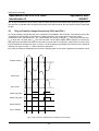
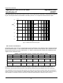
BIT 7
D7
w.
Direct after off-hook the micro-computer has to put the PCD3316 in CAS receive mode. Therefore, in the mode
registers of the PCD3316 the CAS bit has to be set to logic “1”, the FSK bit has to be set to logic “0” and the
XTAL bit has to be set to logic “1” via the I2C-bus. TABLE 3 shows the final contents of the PCD3316 mode
registers at CAS receive mode.
TABLE 3 PCD3316 Mode register contents at CAS receive mode
BIT 6
BIT 5
BIT 4
BIT 3
BIT 2
BIT 1
D6
D5
D4
BIT 0
D3
D2
D1
D0
INT Polarity
“1”
RES
“0”
RES
“0”
RES
“0”
RES
“0”
RES
“0”
Mode register 1 CIDMD1; address 04H; read/write
FSK BOM-mask
“0”
ww
FSK
“0”
CAS
“1”
POL
“0”
Mode register 2 CIDMD2; address 05H; read/write
XTAL
“1”
TB
“0”
SEC/MIN
“0”
INT-SUP
“0”
VERSION 1 VERSION 0
“0”
“0”
The interrupt polarity needed depends on the hardware/ software used, we use the active high posibility.
If a CAS tone is received by the PCD3316, it generates an interrupt request on the IRQ ouput pin, the microcomputer reads the internal registers of the PCD3316 and takes the necessary actions to make FSK receiving
after this possible. The complete CAS receive control flow is given in Fig.7.
19
Philips Semiconductors
Application of the PCD3316 Caller
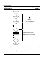
Identification IC
m
Application Note
AN98071
IRQ output
co
CAS receive
LOW
Read Interrupt
status register
NO
Interrupt register, bit 1
-d
CAS interrupt
z.
HIGH
YES
Delay of 50 ms.
MUTE = Active
yc
Transmission circuit off, DTMF on.
Send “D” 60 ms
DTMF generator 1633 and 941 Hz
CAS-bit = “0”, FSK-bit = “1”
(see FSK receive part)
Start timer 550 ms
Time-out, tested in FSK recieve part
w.
Put PCD3316 in
FSK receive mode
goto
FSK receive
Fig.7 CAS receive control procedure
ww
After receiving a CAS tone a 550 ms timeout is necessary because it is not allowed to mute the transmission part
for more than 600 ms. If the first FSK-byte is not received before this time-out expires, the power down mode of
the PCD3316 is entered.
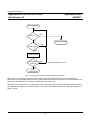
4.2
FSK receiving
An FSK transmission (as specified by BT and Bellcore) consist of a channel seizure (on-hook) which is
transmitted first (sequences of 1010....), followed by a block of marks (all 1’s) finalised by the data. These mark
bits are detected by the PCD3316 which sets the FSK-BOM indication bit (Status register, bit 4). This bit is reset
when the FSK receiver is disabled (see Fig.8). A logic ‘0’ is presented by a signal of 2200 Hz and a logic ‘1’ by
1200 Hz. The baudrate is 1200 Hz.
20
Philips Semiconductors
Application of the PCD3316 Caller
Identification IC
Application Note
AN98071
mark
data
co
channel seizure
m
FSK transmission
ok, full pagewidth
FSK BOM
MBH979
z.
Fig.8 FSK transmission specification (on-hook)
ok, full pagewidth
START
read 2by
I C activity
serial interface
D1
D2
D3
D4
D5
D6
D7
STOP
yc
IRQ
D0
-d
If the FSK BOM-mask bit is set (mode register 1, bit 6), the FSK receiver will wait till this FSK-BOM indication bit
is set (reset after a “0” and less then eleven “1”), and will then generate an interrupt after it has received a
complete data word. An FSK data word consists of one start bit (space), followed by eight data bits and several
stop bits (mark). Interrupt will not be generated during the channel seizure and during the blocks of marks (see
Fig.9) when the FSK BOM-mask is set.
MBH981
w.
Fig.9 IRQ generation after reading a valid data byte
When this FSK BOM-mask bit is not set (mode register 1, bit 6), the FSK receiver will not wait with the generation
of interrupts until a Begin of Mark (BOM) has been detected but will handle the channel seizure as normal data.
The mark bits will still not generate interrupts, because there are no start bits.
ww
This FSK data is available in the FSK data register and can be read by the µC via the I2C-bus.
Hardware considerations:
The FSK inputs of the PCD3316 have to be connected symmetrically with the line terminals without attenuation
to detect FSK signals down to −40 dBm. Series components are required for DC blocking and high voltage
protection by means of the components Cxfsk (C1fsk and C2fsk) and Rxfsk (R1fsk and R2fsk) as shown in Fig.10 as
well as in the application of Fig.31.
Rxfsk calculation: 2 x Rxfsk << ZiFSK (1.4 MΩ typical) to prevent signal loss from the line to the inputs. Rxfsk have
to reduce also the currents into the FSK pins below the specified 10 mA-max. at maximum line signals. A value
of 2 x 100 kΩ is chosen as shown in Fig.31.
The maximum input current into the internal protection diodes, is limited to 1.0 mA-peak at 200 V-peak between
the line terminals.
21
Philips Semiconductors
Application of the PCD3316 Caller
Identification IC
Application Note
AN98071
R1fsk
Cr
Ringer bridge
Vline
C1fsk
co
a/b
m
Cxfsk calculation: Cxfsk/2 > 1/(2 . π . f . Rt) (F) to prevent signal loss;
with f > 1100 Hz and Rt = 2 . Rxfsk + ZiFSK = 1.6 MΩ the value of Cxfsk has to be more than 180 pF.
Chosen is Cxfsk = 1 nF. The minimum voltage for Cxfsk = 200 V-peak.
FSKIN+
POL detection
+
PCD3316
POL detection
FSKIN−
Cr
C2fsk
z.
b/a
R2fsk
R1fsk = R2fsk
Ringer stage
C1fsk = C2fsk
-d
Fig.10 Signal path of FSK signals from line to FSK-inputs
The signal loss from line to FSK inputs at the FSK frequencies measures about 2.8 dB according Fig.11.
(LIN)
yc
0.0
-1.0
-2.0
[dB]
-3.0
w.
-4.0
− 10 dBm
-5.0
-6.0
-7.0
ww
-8.0
-9.0
-10.0
freq. [Hz]
300.0
1.0k
Fig.11 Transfer from line to FSK inputs
22
10.0k
Philips Semiconductors
Application of the PCD3316 Caller
Identification IC
Application Note
AN98071
SW / Control considerations:
BIT 7
D7
TABLE 4 PCD3316 Mode register contents at FSK receive mode
BIT 6
BIT 5
BIT 4
BIT 3
BIT 2
BIT 1
D6
D5
D4
Mode register 1 CIDMD1; address 04H; read/write
FSK BOM-mask
“1”
CAS
“0”
POL
“0”
Mode register 2 CIDMD2; address 05H; read/write
XTAL
“1”
TB
“0”
SEC/MIN
“0”
INT-SUP
“0”
BIT 0
D3
D2
D1
D0
INT Polarity
“1”
RES
“0”
RES
“0”
RES
“0”
RES
“0”
RES
“0”
z.
FSK
“1”
co
m
After CAS, ringer burst, or polarity change the PCD3316 has to be put in FSK receiving mode. Therefore in the
mode registers of the PCD3316 the FSK bit has to be set to logic “1”, the CAS bit has to be set to logic “0”,
because we only want interrupts at real FSK-data receiving the FSK BOM-mask bit has to be set to logic “1” and
the XTAL bit has to be set to logic “1”. TABLE 4 shows the final contents of the PCD3316 mode registers at FSK
receive mode.
VERSION 1 VERSION 0
“0”
“0”
-d
Because here only the FSK part is switched-on it is not necessary to activate the interrupt suppression bit (Mode
register 2, bit 4 = “0”), however if the minute/seconde interrupt is on (for clock or timer purposes) it is necessary
to activate (Mode register 2, bit 4 = “1”), so that during FSK reception these interrups are suppressed
automatically.
In CID application it is necessary to make/keep the POL interrupt active during FSK receive. It must be possible
to receive outside the FSK-bytes also the next ringer signal.
yc
The FSK receive part needs a lot of process power and may not to long be activated, therefore it is protected by
a time-out. During receiving FSK-byte this timer is loaded by the FSK receive part itself, at first activation after
CAS, ringer burst, or polarity change these program part will load the timer.
ww
w.
If a FSK byte is received by the PCD3316, it generates an interrupt request on the IRQ ouput pin, the microcomputer reads the internal registers of the PCD3316 and takes the necessary actions to make FSK receiving
after this possible. The complete FSK receive control flow is given in Fig.12.
23
Philips Semiconductors
Application of the PCD3316 Caller
Identification IC
Application Note
AN98071
co
Time-out = 0
m
FSK receive
YES
NO
z.
IRQ output
RETURN
LOW
HIGH
-d
Read Interrupt
status register
It will return to the privious
mode, CAS, ringer or polatity
change.
FSK interrupt
NO
Interrupt register, bit 5
yc
YES
Read FSK-byte
FSK-data register; address 01H
Data stored in micro-controller RAM
Start timer 150 ms
Time-out, wait 150 ms for next byte
w.
Store received byte
ww
Last FSK-byte NO
received
YES
end
FSK receive
Fig.12 FSK receive control procedure
In off-hook mode it is possible that mark bits are sent after the last received FSK-byte. Therefore it is necessary
that the low level bit of the PCD3316 is polled before this procedure is ended. Then also the mute can be
deactivated. If all FSK-bytes are received the caller id information can be put on a display.
To be sure that no problem occurs during FSK receive the status register of the PCD3316 has to be read too.
Two error bits are available to indicate synchronization problems. FSK-OVR error bit (status register, bit 3)
indicates that a previous byte is lost due to an overrun, FSK-FRM error bit (status register, bit 2) indicates an
incorrect start- or stop-bit.
24
Philips Semiconductors
Application of the PCD3316 Caller
Identification IC
Application Note
AN98071
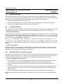
Ring or Polarity Change Detection by POL0 and POL1
co
4.3
m
The on-chip level detector can be used to detect a carrier loss during FSK transmission (interrupt register, bit 4).
The data can be rejected when the signal level is below the reference level, this to avoid that noise is interpreted
as data.
z.
For ring and polarity change detection two comparators are available in the PCD3316. The reference level of the
comparators is set internally by the reference voltage generator. The voltage levels on the two polarity
comparators inputs, POL0 and POL1, are compared with the reference voltage Vref. If input POL0 is lower than
Vref or input POL1 is higher than Vref, bits POL0 and POL1 of the status register (status register, bit 7 and 6) are
high respectively and these bits become low if POL0 is higher than Vref and POL1 is lower than Vref. Every time
the POL0 status bit changes from logic 1 to logic 0, a POL0 interrupt is generated. Every time the POL1 status bit
changes from logic 0 to logic 1, a POL1 interrupt is generated.
-d
Fig.13 shows the above explained POL0 and POL1 handling when a sine-wave is applied on the telephone lines.
w.
POL0 input
yc
Voltage a/b line
POL1 input
ww
Status Reg. Bit 7
Status Reg. Bit 6
POL0 interrupt
POL1 interrupt
Fig.13 POL0 and POL1 handling with a sinewave as input signal.
25
Philips Semiconductors
Application of the PCD3316 Caller
Identification IC
Application Note
AN98071
m
The period time of a POL1-POL0-POL1 sequence is available in the ringer period register in multiples of
1/2048 s. At power-up and in all other cases that a POL1 is available, the contents of the ringer period register is
255.
Polarity Change is that only POL1 or POL0 is generated while the contents of the ringer period register is 255.
co
Ringer is that there is a sequence of POL1-POL0-POL1-etc, while at the second POL1 after a POL0 the
contents of the ringer period register is the time of the previous POL1-POL0-POL1 sequence.
Only the 32 kHz clock is needed for the ringer or polarity change detection.
Hardware considerations:
z.
The ringer frequency is converted into a binary number when a sequence of POL0-POL1-POL0 interrupts is
generated; see before in this chapter or in [1]. To generate the POL0-POL1-POL0 interrupt sequence the input
signals of POL0 and POL1 have to exceed Vref = 1.25V and must have a phase shift of a half-period between
each other, as shown in Fig.13.
The POL inputs of the PCD3316 have to be connected with the line via attenuators by using the ringer capacitors
as shown in Fig.14.
-d
To detect the ringer signals or polarity changes the input voltage at POL0 and POL1 has to exceed Vref = 1.25 V
(± 125 mV). The minimum ringer voltage at the line, to be detected, can be calculated as follows by using the
attenuator components Rpol1 and Rpol2 of POL1 input as shown in Fig.30:
vringer-min = Vref . (Rpol2//Zipol + Rpol1) / [√2.(Rpol2// Zipol)] (Vrms)
with Vref = 1.25 V, Rpol1 = 820 kΩ, Rpol2 = 100 kΩ, Zipol > 1.25 MΩ the calculated value of
vringer-min = 8.7 Vrms.
yc
This is a theoretical value in case the line is not loaded with the ringer stage of the set. The real minimum ringer
voltage which is detected by the PCD3316, as applied in the application of chapter 6.1, is about 13 Vrms due to
the voltage drops across the 2.2 µF ringer capacitors Cr.
w.
Note that the application of chapter 6.1 is provided with the UBA1702 which has an internal ringer threshold. This
ringer threshold, which can be adjusted, determines the minimum ringer voltage at which the ringer capsule is
activated. Without UBA1702 the minimum ringer voltage has to be adjusted by the ratio of the Rpolx resistors.
a/b
Cr
Ringer bridge
ww
Vringer
b/a
Rpol0
POL0
Rpol3
+
Rpol2
PCD3316
POL1
Cr
Rpol1
Rpol0 = Rpol1
Ringer stage
Rpol3 = Rpol2
Fig.14 Signal path of ringer signal from line to POL-inputs
26
Philips Semiconductors
Application of the PCD3316 Caller
Identification IC
Application Note
AN98071
-18.0
m
The signal transfer from line to POL-inputs is shown in Fig.15 with the POL attenuation components as shown in
Fig.30. The low pass effect in the transfer is caused by the two 4.7 nF capacitors across the POL inputs.
(LIN)
co
vline = +10 dBm
-20.0
[dB]
z.
-22.0
-24.0
-26.0
-d
-28.0
-30.0
10.0
100.0
freq. [Hz]
1.0k
yc
Fig.15 Transfer from line to POL inputs
SW / Control considerations:
BIT 7
D7
w.
Immediately after reset, the micro-computer has to put the PCD3316 in POL detection mode. Therefore the POL
bit has to be set to logic “1”. The CAS and FSK functions are normal off to save power, but it is allowed to have
these functions active too (CAS or FSK bit also “1”). TABLE 5 shows the final contents of the PCD3316 mode
registers at POL detection mode.
TABLE 5 PCD3316 Mode register contents at POL detection mode
BIT 6
BIT 5
BIT 4
BIT 3
BIT 2
BIT 1
D6
D5
D4
BIT 0
D3
D2
D1
D0
INT Polarity
“1”
RES
“0”
RES
“0”
RES
“0”
RES
“0”
RES
“0”
Mode register 1 CIDMD1; address 04H; read/write
FSK BOM-mask
“0”
ww
FSK
“0”
CAS
“0”
POL
“1”
Mode register 2 CIDMD2; address 05H; read/write
XTAL
“0”
TB
“1”
SEC/MIN
“0”
INT-SUP
“0”
VERSION 1 VERSION 0
“0”
“0”
Distinction between the detection of a polarity change or ringer detect has to be made by software. The
PCD3316 only generates POL0 and POL1 interrupts and measures the time between two POL1 interrupts.
The explanation of this control has been split-up into three parts, first there is tested if there was a POL0/POL1
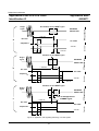
activity on the line, second selection is made between polarity change and ringer and final the ringer frequency
and activation is controlled. The first control flow, detect the first POL0/POL1 activity is given in Fig.16.
27
Philips Semiconductors
Application of the PCD3316 Caller
Identification IC
m
Application Note
AN98071
LOW
HIGH
Read Interrupt
status register
NO
Interrupt register, bit 2 or 3
-d
POL0/POL1
interrupt
z.
IRQ output
co
IDLE
YES
Start timer 50 ms
Time-out, wait 50 ms for next POL0/1
yc
goto
Polarity/Ring test
Fig.16 POL0/POL1 detection procedure
ww
w.
After preforming the above described test we know that there is activity on the telephone lines. However if it is
polarity change or ringer we need the second control procedure. To decide between the two posibilities the timer
is loaded with the lowest possible time between two POL0/POL1 interrupts if its is a ringer signal (50 ms means a
ringer frequency of 10Hz or higher). The second control flow, selection between polarity change and possible
ringer frequency, is given in Fig.17.
28
Philips Semiconductors
Application of the PCD3316 Caller
Identification IC
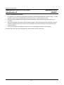
m
Application Note
AN98071
Time-out = 0
co
Polariry/Ringer
YES
NO
z.
IRQ output
Polarity change
LOW
HIGH
-d
Read Interrupt
status register
NO
Interrupt register, bit 2 or 3
yc
POL0/POL1
interrupt
YES
goto
Ringer detect
w.
Fig.17 Polarity change and ringer frequency detection procedure.
When the time-out expires (no POL0 or POL1 interrupt detected) there was only a polarity change on the
telephone line. In the BT application this will be used as start of the Caller ID procedure. In other applications this
will be seen as a disturbance and will be switched back to the IDLE part.
ww
Still we are not sure that there is a valid ringer signal on the telephone line. Herefore the ringer frequency has to
be measured and validated. The final POL0/POL1 control flow, the detection if there is a valid ringer frequency, is
given in Fig.18.
29
Philips Semiconductors
Application of the PCD3316 Caller
Identification IC
m
Application Note
AN98071
co
Ringer detect
Start timer 100 ms
Time-out, wait 100 ms for next POL1
YES
z.
Time-out = 0
Stop ringer
generation
NO
LOW
-d
IRQ output
HIGH
yc
Read Interrupt
status register
POL1 interrupt
NO
Start timer 4 s
goto
FSK receive
Interrupt register, bit 3
YES
w.
Read Ringer-byte
ww
Ringer frequency
Ringer-period register; address 03H
INVALID
VALID
Start ringer
generation
Stop ringer
generation
Fig.18 Ringer frequency detection procedure.
In the ringer detection part only the POL1 interrupt has to be tested, because only after a POL1 interrupt the
ringer period register is reloaded with a new value.
If no new POL1 interrupts are generated, because the ringer has stopped, the implemented timer will
automatically stop the ringer generation and prepare it for FSK receiving. The 4s time-out will be tested in the
FSK receive part.
30
Philips Semiconductors
Application of the PCD3316 Caller
Identification IC
4.4
Application Note
AN98071
Power Down state
m
The PCD3316 can be forced in a Power-down state by switching off the 3.58 MHz system clock and the A/D
converter. This is done by setting mode register 2, bit 7 to logic 0. To guarantee correct operation, otherwise the
PCD3316 stays in the selected function, the following order of actions must be performed:
Switch-off CAS and FSK detection (if turned on).
2.
Read the interrupt register, thus cleaning pending interrupts generated by the CAS and FSK detector.
3.
Switch-off the 3.58 MHz oscillator by reset bit 7 of mode register 2.
4.5
co
1.
Low Battery Detect
z.
The PCD3316 has an extra comparator to guard the battery voltage. If the voltage on the LOWBAT input is less
than the reference voltage Vref, the LOW_BAT indication (status register, bit 5) is high, otherwise it is low.
Hardware considerations:
-d
A tap of the battery voltage has to be connected with the LOWBAT input to monitor the minimum working voltage
of the PCD3316 and PCD3755F or other type of µC. Detection level of the PCD3316 is Vref = 1.25 V ± 125 mV.
For a VDD-minimum = 2.5 V, detection has to be done at VBBbat = 2.5 + 0.125 + VD123 + (VBB − VDD) following
the supply structure of the application of chapter 6.1.
With VD123 = 0.6 V and (VBB − VDD) = 100 mV (2.5 V < VBB < 3.0) the minimum level of VBBbat = 3.32 V.
In this case with 3 x 1.5 V batteries, an attenuation of a factor 0.414, from VBBbat to LOWBAT, has to be made.
At Rlow1 = 1 MΩ the value of Rlow2 has to be 1.5 MΩ. The input current into LOWBAT, which is < 1 nA, can be
neglected.
yc
Control considerations:
Because the setting of the LOW-BAT bit (status register, bit 5) generates no interrupt on the IRQ pin, this bit
should be polled. A practical solution is to read the status register value when a minute or second interrupt is
generated, and put the low battery indication on the display.
4.6
Real-Time-Clock or Call-Timer signal
w.
The PCD3316 doesn’t have a real-time-clock or call-timer hardware on-board, but with the 32 kHz oscillator the
time base is able to generate either a 1 second or a 1 minute interrupt signal which can be used by the microcomputer to make a real-time-clock or a call timer. After reading the interrupt the interrupt is reset.
Control considerations real-time-clock:
For real-time-clock you need the minute interrupt generation, therefore the TB bit has to be set to logic “1”
(mode registers 2, bit 6) and the SEC/MIN bit has to be set to logic “0” (mode register 2, bit 5).
ww
1.
2.
Every minute the PCD3316 generates an interrupt request via pin IRQ of the PCD3316 to the microcomputer.
3.
The micro-computer will read the “interrupt status register” of the PCD3316 and tests if the MIN interrupt
(interrupt register, bit 7) is set, if yes the micro-computer will continue with point 4, else it waits for next
interrupt (point 2).
4.
The micro-computer will update the real-time-clock, put it on the display and wait for next interrupt.
Because normal Caller ID messages include the present time, this can be used to synchronise this real-timeclock.
31
Philips Semiconductors
Application of the PCD3316 Caller
Identification IC
Application Note
AN98071
Control considerations call-timer:
For call-timer you need the second interrupt generation, therefore the TB bit has to be set to logic “1” (mode
registers 2, bit 6) and the SEC/MIN bit has to be set to logic “1” (mode register 2, bit 5).
2.
Every second the PCD3316 generates an interrupt request via pin IRQ of the PCD3316 to the microcomputer.
3.
The micro-computer will read the “interrupt status register” of the PCD3316 and tests if the SEC interrupt
(interrupt register, bit 6) is set, if yes the micro-computer will continue with point 4, else it waits for next
interrupt (point 2).
4.
The micro-computer will update the call-timer, put it on the display and wait for next interrupt.
co
m
1.
ww
w.
yc
-d
z.
Of course every time you start a new telephone call this timer has to be set to zero.
32
Philips Semiconductors
Application of the PCD3316 Caller
Identification IC
5.
Application Note
AN98071
APPLICATION PROPOSALS
co
m
This chapter describes application proposals of the PCD3316 CID / CIDCW receiver IC elucidated with block
diagrams and timing diagrams as far as useful. Proposed are a ‘Basic set’, an ‘Adjunct box’ and application
adaptions to meet the British Telecom (BT) and France Telecom (FT) requirements. Only the most important
parts of the applications are shown in the block diagrams while the descriptions are kept briefly. The PCD3316 is
described in this report and specified in [1]. Details of the other ICs: transmission IC TEA1112, microcontroller
PCD3755F, ringer/interrupter UBA1702, handsfree IC TEA1093 can be found in [3] while applications are shown
in [4].
The applications in this chapter have to be seen as proposals only, which are not built and not tested.
Basic telephone set with CID / CIDCW
z.
5.1
This basic application with CID / CIDCW functions is meant for ‘Bellcore’ oriented countries. The blockdiagram is
shown in Fig.19 using the TEA1112, PCD3316, microcontroller, display and discrete ringer. Realized and tested
applications with the PCD3316 are described in chapter 6. The microcontroller must be a type with DTMF
generator on chip (for instance the PCD3755F).
-d
Transmission / dialling
yc
The TEA1112 takes care of the interface between the microphone and ear capsule of the handset and the line
while during DTMF dialling the tones from the µC are transmitted to the line. The transmission functions are line
powered. The discrete ‘hook-switch’, shown in Fig.19 as a simple switch, is controlled by the µC via DP/FL to
perform line interruptions for pulse dialling and flash. After lifting the ‘cradle switch’ the hook-switch is activated
while the µC is set in the transmission mode via CSI and CE. The dialling function are available while the display
is informed via the I2C - bus.
Ringing
w.
The ringer circuitry, built up with discrete components, contains ringer supply and volume control. The PCD3316
generates an IRQ signal when a ringer voltage is detected on the POL inputs and activates the microcontroller by
means of CE. The microcontroller generates a ringer tone when the ‘binary representation’ of the ringer
frequency from the PCD3316 is detected as a valid frequency. The ringer stage drives the PXE ringer capsule.
Volume control (if available in the ringer stage) is controlled by the microcontroller via the keypad.
PCD3316 - CID / CIDCW
The PCD3316 communicates with the microcontroller by means of the I2C - bus. Timing of the CAS and FSK
functions is derived from the 3.58 MHz oscillator of the microcontroller. The 32 kHz oscillator activates the
LOWBAT, Ring and Polarity detectors.
ww
The CID / CIDCW signals from the line as ringing, polarity change and FSK signals are attenuated and band
filtered before entering the device inputs of the PCD3316. The CAS signal is derived from the receiver output of
the TEA1112 to separate the CAS signal from own speech by means of the anti side-tone network of the circuitry
around the TEA1112.
The LOWBAT input of the PCD3316 detects too low battery voltages. During on-hook, the PCD3316 is in PD with
the 32 kHz oscillator running while the microcontroller is in stop mode. Polarity changes or ringing signals from
the line are detected by the PCD3316. The PCD3316 wakes-up the microcontroller (IRQ + CE) while the
microcontroller activates, on his turn, the PCD3316 via the I2C - bus to receive CAS and FSK signals.
VDD supply
The PCD3316, microcontroller and display are supplied by VDD. Battery support is necessary during off-hook
because the VCC supply point is too weak to deliver enough current, at low line voltages, for the microcontroller
and PCD3316 and display. At higher line voltages VCC could contribute.
33
Philips Semiconductors
Application of the PCD3316 Caller
Identification IC
Application Note
AN98071
co
m
During on-hook, current consumption is rather low due to the PD or stop mode of the PCD3316 respectively
microcontroller which saves battery energy. The devices becomes operational when polarity changes or ringing
signals from the line are detected resulting in an increase of the current consumption from VDD. If required the
supply of the devices during ringing could be delivered by the ringer stage. Consult chapter 6.1.5 concerning
supply structure.
a/b
+
+
z.
Cradle switch
b/a
Interrupter
QR
+
-d
Filters
&
Attenuators
Ringer
SLPE
VCC TEA1112
VEE
3.3V DC
VDD
MIC
LN
BAT
3 x 1.5 V
DTMF
MUTE
regulator
Ringer tone
yc
Volume control
VDD
FSKIN POL
VDD
VDD
DP/FL CSI
CE/FDI
CAS LOWBAT
VDD
IRQ
DISPLAY
PCD3316
w.
LX
VEE SDA/SCL
SDA/SCL
VOL DTMF
MUTE
IRQ
microcontroller
3.58 MHz
HX
VDD
XTAL
GND/AGND
SDA/SCL
VSS
ww
32 kHz
LINE INFO
Ringer tone
Vol.control
DP/FL
I2C - BUS
KEYPAD
OPTIONAL DEVICES
VDD
QR
UBA1702
Vol.control
Interrupter
Ringer
VDD stabilizer
LN
VBB
TEA1093
Hands free
SLPE
Fig.19 Block diagram of basic telephone set with CID/CIDCW functions
34
Philips Semiconductors
Application of the PCD3316 Caller
Identification IC
Application Note
AN98071
Optional functions
ww
w.
yc
-d
z.
co
m
Fig.19 shows also the TEA1093 and the UBA1702 to create a number of extra or optional functions.
Furthermore, the discrete ringer part and hook-switch of the basic set can be replaced by the UBA1702 while the
UBA1702 offers also a stabilized VDD voltage of 3.3 V using the battery voltage or ringing voltage as input. See
chapter 6.1.
The TEA1093 can be applied to design a handsfree telephone set. This device contains a loudspeaker amplifier
supplied from the line. Application examples of the TEA1093 can be found in [4].
35
Philips Semiconductors
Application of the PCD3316 Caller
Identification IC
5.2
Application Note
AN98071
Caller ID / Call Waiting Adjunct box
co
m
A standalone Adjunct Box with the PCD3316 is proposed in this chapter. It has to be connected between the
telephone line and telephone set by means of two plugs as indicated in Fig.20. The box contains circuitry to
receive and to handle the CID / CIDCW data. A ‘Line Current Sensor’ and a ‘Line Interrupter’ are placed in series
with the external telephone set to detect the line current flowing to the telephone set respectively to switch-off the
telephone set from the line. The Line Interrupter has to be ‘normally closed’ when it is not activated; see the Note
at the end of this chapter about the details.
Line Interrupter
a/b
z.
diode bridge
+
Telephone
line
External
telephone
set
Line Current
Sensor
b/a
a/b
b/a
-d
Electronic
hook switch
Line termination
Decoupling
DC - stabilizer
&
Attenuators
Transmit - stage
yc
Supply
3.3V DC
+
VDD
regulator
BAT
3 x 1.5 V
w.
VDD
VDD FSKIN
POL
CAS LOWBAT
HX
ww
GND/AGND
VDD
VDD Tone Reset LINE OHD TMS
VDD
XTAL
µC
IRQ
IRQ
PCD3316
SDA/SCL
3.58 MHz
VDD
DISPLAY
CE/T0
LX
SDA/SCL
VSS
P1.X
SDA/SCL VEE
32 kHz
I2C - BUS
KEYPAD
adjunct box
Fig.20 Block diagram of an Adjunct box
The adjunct box has its own line voltage stabilizer and line termination to adapt the box to the line when the
external telephone set is switched-off from the line in off-hook mode. The transmit stage of the adjunct box is
used to send a DTMF acknowledge signal to the line. FSK, POL and CAS signals from the line are offered to the
36
Philips Semiconductors
Application of the PCD3316 Caller
Identification IC
Application Note
AN98071
co
m
PCD3316 via decoupling capacitors, attenuators and filters if required. The PCD3316 has its 32 kHz oscillator to
detect polarity and ringing signals from the line in power down mode while the 3.58 MHz timing signal is delivered
by the microcontroller. Information between PCD3316, microcontroller and display is provided by the I2C circuitry
of the devices and the I2C - bus. The keypad could be applied to set the pre-conditions of the display, to handle
the stored numbers and names and for Call Back facilities. The adjunct box is battery supplied as indicated in
Fig.20. Mains supply via a transformer can be an option.
-d
z.
The following states are described as follows:
Telephone set in on-hook: The Line Interrupter is closed; the ringing signal can reach the telephone set in
on-hook mode. The adjunct box is in standby mode. Both are ready to receive CID / CIDCW and ringer signals.
The PCD3316 detects the polarity changes or ringing signals to wake-up the controller via the IRQ signal and to
receives the FSK signals afterwards.
The ringing sounds are produced by the telephone set. When the handset of the telephone set is lifted (off-hook
mode) the DC line current will be detected by the controller via the Line Current Sensor. The Line Interrupter
remains closed.
Telephone set in off-hook: The telephone set terminates the telephone line and stabilized the voltage across
the set. The controller is informed about the off-hook status of the telephone set. PCD3316 and controller are
both operational, ready to receive and to process the CIDCW info entering the line. After the CAS tone has been
detected by the PCD3316, the external telephone set is switched-off from the line by means of the Line
Interrupter. The DC stabilizer and the line termination of the adjunct box are activated by the controller during
‘muting’ the telephone set. Acknowledgement can be sent to the line and FSK data can be received. At the end of
the messages the telephone set takes-over the line interface functions from the adjunct box.
yc
The line interface of the adjunct box has to be designed according country requirements regarding BRL, line
voltage, DTMF signal level etc. Application adaptions to handle CID / CIDCW messages according the BT
specifications are discussed in the chapters 5.3.
ww
w.
Note: The Line Current Sensor and Line Interrupter could be realised by Solid State Sensor respectively by a
Solid State Switch or relays.
37
Philips Semiconductors
Application of the PCD3316 Caller
Identification IC
5.3
Application Note
AN98071
Application for British Telecom (BT)
silence
Data
End of
V.23
Signals
Ringing
NETWORK
Mark
-d
SIGNALLING
20 ± 5 ms
> 25 mA
‘DC wetting pulse’
< 0.5 mA
Zset = ‘HIGH’
yc
Zset = ‘Zss’
DC LOAD
AC LOAD
15 ± 1 ms
H
L
>=45 ms
80-262 ms
45-75 ms
<=2.5 s
>200 ms
LOW LEVEL
BIT
CID-DC
ww
H
L
88-110 ms
100 ± 50 ms
w.
>=100 ms
BT Requirements
silence
Channel
Seizure
H
L
CID-AC
PCD3316
Idle State
Alert Signal
Controller
Line
Reversal
z.
co
m
Application for BT requires adaptions, SW and HW, of the basic application of Fig.19 because the CIDCW
signalling procedure deviates from ‘Bellcore’. During on-hook (Idle state) the ‘Network Signalling’ is shown in
Fig.21. The signalling starts with a reversal of the DC line voltage followed by an ‘Alert Signal’, ‘Channel Seizure’
and FSK data before the ringing signal is generated.
The line current has to be increased from almost ‘zero’ (idle state) to > 25 mA at 20 ± 5 ms after the ‘Alert Signal’
during 15 ± 1 ms. The set impedance (on-hook) must alter from ‘high’ (idle state) to a defined value at 20 ± 5 ms
after the ‘Alert Signal’. The BRL of the set is specified with respect to Zss = 827 Ω + 1386 Ω // 139 nF for a
frequency range from 200 Hz to 4 kHz. The line current as well as the set impedance have to return to their
original state within 100 ± 50 ms when the V.23 signalling is ended. Consult the BT specification [12] about
specification of ‘idle state’ concerning line current and set impedances.
Fig.21 BT application; Down stream signalling and timing of control signals
Normally the FSK-Alert Signal can be detected by the FSK receiver of the PCD3316. However the detection
range of the FSK frequencies of the PCD3316 is specified as ± 0.5%, while the FSK ‘Alert Signal’ from BT can
deviate with ± 1.1% which can result in detection failures. The PCD3316 uses in this case the ‘Low Level Bit’
38
Philips Semiconductors
Application of the PCD3316 Caller
Identification IC
Application Note
AN98071
m
from the interrupt register which is set (to ‘high’), when the level of the ‘Alert Signal’ stops and reduces below the
− 37.8 dBm (max.) detection level of the PCD3316, see Fig.21.
a/b
Cr
+
+
co
The controller has to control the DC load and AC load, shown in Fig.22, by means of the two signals: CID-DC and
CID-AC. SW has to be written for this purpose.
Cradle switch
z.
Transmission IC
Cr
b/a
AC load
Ringer
DC load
-d
100 Ω
1370 Ω
‘Zss’
Filters & Attenuators
FSK and CAS tones
Rw
CID-DC
825 Ω
CID-AC
yc
Polarity changes
120 nF
w.
Fig.22 BT application; circuit adaption to basic set of Fig.19
Fig.22 shows a proposal of the adaption to the basic application of Fig.19 to meet the BT requirements. Both
blocks: DC load and AC load are controlled by the µC as explained before. The line current is switched to > 25
mA while the switched set impedance has to approximate ‘Zss’. Fig.22 shows the AC load with current
components values.
ww
Take into account that the impedance of the ringer circuitry of the set is present in this on-hook state for ringer
signals. However, the influence of the ringer stage can be neglected. The ringer bridge is not conducting at the
low test levels (maximum − 2.2 dB) during the time that the set impedance has to be adapted.
The AC load is connected in series with the capacitors Cr of the ringing circuit to prevent any DC currents from
the line.
39
Philips Semiconductors
Application of the PCD3316 Caller
Identification IC
5.4
Application Note
AN98071
Application for France Telecom (FT)
co
m
Application for FT requires adaptions, SW and HW, of the basic application of Fig.19 because the CIDCW
signalling procedure deviates from ‘Bellcore’. The impedance of the set has to be reduced from ‘idle’ to a fixed
value after the first ring signal and has to return to ‘idle’ within a certain time depending on the conditions of the
Channel Seizure Signal.
Consult [13], paragraph 2.1.2 where this signal is specified as ‘SMMR’ signal, offering 300 bits of alternating 0’s
(1200 Hz) and 1’s (2200 Hz).
The first ‘ring’ signal of > 25 Vrms with a duration between the 200 ms and 300 ms, indicates that CID info follows
while the ringer detection is not allowed; thus ringer sound not produced. Ringer signals have to be detected as a
valid ringer signal at signal durations of > 400 ms.
z.
The adapted Zset, during a certain time interval, is specified as BRL in dB’s. The BRL has to be more than 14 dB
with respect to 1200 Ω for frequencies from 1 kHz up to 2.5 kHz. Take into account that the impedance of the
ringer circuitry of the set is present in this on-hook state for ringer signals. However, the influence of the ringer
stage can be neglected due to the low test levels for which the ringer stage is not conducting.
-d
The HW has to be adapted regarding the set impedance by applying the AC load configuration drawn in Fig.22 of
chapter 5.3, with adapted components values obviously. This load has to be switched across the line during the
indicated time interval in Fig.23 by means of controller signal CID-AC. The SW has to be adapted for this
purpose.
Fig.23 shows the different conditions for which the Zset has to be adapted which are:
a: No validation of the ‘SMMR’ signal. The line impedance has to be adapted to Zset between 200 ms and
350 ms after the ring signal and has to return to idle state within 1450 ms + < 150 ms.
yc
b: Validation of the ‘SMMR’ signal. Zset has to return to idle state within 420 ms + < 150 ms after validation of
the ‘SMMR’ signal.
ww
w.
c: Disappearance of the ‘SMMR’ signal after validation. Zset has to return to idle state within 150 ms after
validation of the ‘SMMR’ signal in case the signal disappears for more than 40 ms. The disappearance of the
‘SMMR’ signal can be detected by the ‘Low Level Bit’ of the PCD3316 as indicated in chapter 5.3.
40
Philips Semiconductors
Application of the PCD3316 Caller
Identification IC
NETWORK
co
SIGNALLING
1450 ms
a
idle state
AC LOAD
z.
adapted Zset
200-350 ms
CID-AC
< 150 ms
Controller
m
No validation of the ‘SMMR’ signal
Ringer
signal
FT Requirements
Application Note
AN98071
< 1450 ms
idle state
NETWORK
SIGNALLING
420 ms
yc
b
-d
Ringer
signal
FT Requirements
Validation of the ‘SMMR’ signal
AC LOAD
CID-AC
< 150 ms
Validation of the ‘SMMR’ signal
ww
Ringer
signal
c
NETWORK
SIGNALLING
> 40 ms disappearance
of SMMR signal
< 1450 ms
< 150 ms
FT Requirements
w.
200-350 ms
Controller
adapted Zset
idle state
adapted Zset
CID-AC
200-350 ms
Fig.23 FT application; CID signalling and timing of control signals
41
Controller
AC LOAD
Philips Semiconductors
Application of the PCD3316 Caller
Identification IC
REALIZED APPLICATIONS WITH THE PCD3316
6.1
Bellcore approved telephone set
m
6.
Application Note
AN98071
co
A telephone set with CID / CIDCW functions with the PCD3316, based on the DEMO OM5843, is described in
the following chapters. The OM5843 as documented in reference [2] has been modified, see chapter 6.1.7, to
receive the ‘Bellcore Approval’. Applied ICs besides the PCD3316 are UBA1702, TEA1112, PCD3755F,
PCD3316 and the LCD display with the PCF2116K which are briefly described. Consult [1] and [3] for details of
the concerning ICs while application details are given in [2] and [4].
Hardware description
-d
6.1.1
z.
This chapter is built-up as follows:
- description of the HW
- description of the SW with µC considerations and timing diagrams
- ‘Supply structure’ describing the current structure and ‘Proposals’ to improve it
- POTS mode; what is required and what has to be done to function in POTS mode
- application diagrams Fig.28, Fig.29, Fig.30 and Fig.31
- what’s done to get ‘Bellcore Approval’
The application diagrams are shown in Fig.28, Fig.29, Fig.30 and Fig.31. The HW is briefly described following
the circuitry around the ICs on the board mainly: UBA1702, TEA1112, and finally the supply structure.
Board supply
yc
The transmission part and ringer part of the application, UBA1702 and TEA1112 are supplied by the line via
modular jack P101, selection jumpers and diode bridges. The PCD3755F and PCD3316 are supplied by the
battery according the design of the OM5843. Suggestions to improve the supply are shown in chapter 6.1.5.3.
Line interrupter driver / ringer UBA1702
The UBA1702 performs the high voltage interface and ringer functions in cooperation with the PCD3755F and
TEA1112.
w.
The UBA1702 (or UBA1702A) drives the external switch TR101 applied as hook-switch and line interrupter for
pulse dialling and flash under control of the PCD3755F by means of the DPI signal.
ww
The IC takes care of the current management as current detector and limiter and protection of the voltage across
the transmission IC.
Detection of the line current is set at 3 mA with input CDA open. The PCD3755F will be informed by means of the
CDO signal when Iline > 3 mA.The line current will be limited at Iline > 120 mA in this case, due to the connection
of pin CLA to VEE.
The UBA1702 protects the voltage VLN-VEE across the TEA1112 at 12 V at pin ZPA open.
The stabilized voltage on pin VDD supplies the PCD3755F, PCD3316 and display at 3.3 V. The input voltage of
the internal stabilizer is delivered by the batteries (VBBbat = 4.5 V nominal) on the VBB input. See ‘Supply
structure’ in this chapter.
The ringer input voltage from the line is delivered on pin RPI via C111 and C112, the ringer bridge and R106. The
ringer supply voltage available on pin VRR, is decoupled by C119. Ringer melody and volume control levels are
delivered by the PCD3755F by means of RMI respectively VOL1 and VOL2. The ringer sound is produced by the
PXE capsule H1 which is connected between ROA and ROB when the ringer voltage at the a/b-terminals is more
than 24 Vrms; see description of PCD3755F (CE/FDI input) and PCD3316 (POL inputs). The minimum ringer
level is determined by the internal ‘ringer threshold’ of the UBA1702. The frequency range is determined by SW.
42
Philips Semiconductors
Application of the PCD3316 Caller
Identification IC
Application Note
AN98071
m
Volume control by the keypad by means of the V+ or V− keys results in an increase or reduction of the sound
pressure from the ringer capsule based on 12 dB reduction steps of the RMI signal from maximum to −36 dB.
Transmission / line interface TEA1112
co
The TEA1112 performs the interface between telephone line and transducers such as microphone capsule and
earpiece as well as microcontroller for DTMF and pulse dialling; see Fig.29.
The line voltage Va/b between the a/b-b/a terminals is stabilized by the reference voltage (VLN-SLPE) which is set
at 4.65 V by means of the R109 (15 kΩ) between SLPE and REG. Va/b measures 6.8 V at Iline = 20 mA. The set
impedance Zset of about 600 Ω is mainly determined by R104 (620 Ω).
z.
The send path consists of the microphone bandpass filter, components R125, R129, C118, C120, C130 and
R120, and the microphone amplifier from MIC−/MIC+ to LN. The gain of the microphone amplifier is set by R132.
The output modulation current from LN flowing into Zset in parallel with Zline generates the line signal. The gain
from microphone to a/b-b/a terminals is about 26 dB at Zline = 600 Ω, 1 kHz and Iline = 20 mA. The electret
microphone, connected to jacket P109, is supplied from VCC via diode D100 and the two series resistors R124
and R131.
-d
The receive signal from the line is attenuated by the anti side-tone network, amplified by the receive amplifier
from IR to QR, and supplied to the earpiece (via switches). The gain of the receive amplifier is set by R119. The
gain from a/b-b/a terminals to earpiece is about −10 dB at Iline = 20 mA and 1 kHz. A low pass filter is created by
C117 and R119 into parallel with the internal receive gain setting resistor resulting in f−3 dB = 7.5 kHz.
The CAS signal from the line is available at QR and delivered to the PCD3316 via a high pass filter; see Fig.31.
Input AGC is connected to VEE resulting in a maximum microphone and receive gain below Iline < 26 mA and
6 dB gain reduction at Iline > 61 mA
w.
yc
The DTMF signal from the PCD3755F is attenuated by R101 and R102 and coupled into the DTMF input. The
DTMF levels on the a/b-b/a terminals measures −8/−10 dBm at Zline = 600 Ω and an input signal on pin DTMF of
− 22.5 dBm.
DTMF is activated by pressing one of the keys which enables the DTMF amplifier and disables the receive and
microphone amplifiers (MUTE = HIGH).
MUTE is activated at DTMF dialling and during CID (off-hook) when an acknowledgement is generated and FSK
data is received by the PCD3316.
Microcontroller PCD3755F / I2C-bus
ww
The PCD3755F is an OTP-type microcontroller loaded with derivate-SW from the “Reference Software, version
1.0”; see [9].
The controller takes care of the communication with the PCD3316 and display via the I2C-bus and controls the
UBA1702 and TEA1112 by means of separate signal lines as explained in the HW descriptions of the ICs in this
chapter.
The PCD3755F is supplied by VDD = 3.3 V nominal. The reset input is connected to VSS which means that the
internal reset will be activated at rising VDD voltage.
The matrix keypad, connected with the K1 to K6 inputs, contains besides the standard keys an ‘RCL-key’ for
Flash operations, an ‘AP-key’ for Access Pause, a ‘LNR-key’ for Last Number Redial, a ‘STORE-key’ to store a
telephone number and for toggling between DTMF and pulse dialling an ‘MRC-key’ to recall a telephone number
and the ‘V+/V− -keys’ for volume control of the ringer signal. Consult [2] for store and recall operations.
The CE/FDI input is controlled by the EHI signal from the UBA1702 or by the IRQ signal from the PCD3316. After
lifting the handset, CSI as well as EHI becomes ‘high’ to initialize the controller in the speech mode.
When a valid ringer signal level is detected by the PCD3316, the PCD3316 generates an IRQ signal which
wakes-up the controller via the CE/FDI input and the IRQ input to activate the ringer mode. The PCD3755F
43
Philips Semiconductors
Application of the PCD3316 Caller
Identification IC
Application Note
AN98071
co
Test outputs are available to test the CID functions of the controller.
m
reacts with reading the appropriate registers of the PCD3316 via the I2C-bus. If the PCD3755F determines a
valid ringer frequency, by means of a binary representation from the PCD3316, a ringer melody is generated at
the TONE output with a level of − 11 dBm. An attenuator connected to the TONE output determines the correct
levels of the DTMF signal.
The SCL and SDA line of the I2C bus are pulled-up to the VDD by 47 kΩ resistors.
CID/CW PCD3316
The PCD3316 is supplied by VDD = 3.3 V nominal. DGND and AGND are star-connected with the supply on the
board.
z.
The timing of the PCD3316 is derived from the PCD3755F X-tal oscillator; the 3.58 MHz signal is coupled into the
HXIN input via 3.9 pF. The LF oscillator uses a 32.8 kHz X-tal in parallel with 470 kΩ.
-d
The POL inputs are coupled to the line via the two ringer capacitors of 2.2 µF and a 20 dB attenuator formed by
the four Rpolx resistors. The signals on the POL inputs of the device are clamped to VDD and GND by means of
the internal protection diodes of the PCD3316. A low pass filter is made by the attenuator resistors Rpolx and the
corresponding capacitor C134 or C135 resulting in f−3 dB = 400 Hz.
At ringer voltages on the a/b-terminals of > 13 Vrms, the ringer voltage is detected by the PCD3316 because the
signal at the POL inputs exceeds Vref. The PCD3755F is activated and produces a signal at the TONE output
when the correct frequency is detected. A ringer sound is produced by the PXE capsule at ringer voltages on the
a/b-terminals of > 24 Vrms due to the ringer threshold of the UBA1702.
yc
The FSK signals from the line are directly coupled to the line via 100 kΩ series resistors for input current
protection. A high pass filter is made by Cxfsk and the Zi of the FSKIN+ or FSKIN− input. The cut-off frequency of
this FSK filter is f−3 dB = 200 Hz.
The CAS signal is subtracted from the receiver output of the transmission IC TEA1112. The CAS signal from the
line is attenuated by about 6 dB, at 2.5 kHz, before it enters the CASIN input of the PCD3316. This is due to the
receive gain setting of the TEA1112, the low pass filter at the QR-output of the TEA1112 with f−3 dB = 7.5 kHz
(see TEA1112 description) and the high pass filter at the CASIN input of the PCD3316 with f−3 dB = 800 Hz. This
filter improves CAS tone receiving.
w.
The LOWBAT input is connected with a tap of battery voltage resulting in a detection voltage of VBBbat/2. At
VBBbat < 2.5 V (VDD is reduced to about 2.3 V) the character ‘B’ will be displayed on the LCD.
LCD Display
ww
The LCD display LPH7319-3 with driver PCF2116K is supplied by VDD and controlled via the I2C bus. The
intensity of the display can be set by means of a potentiometer. Most of the PCD3316 functions result in
displayed messages by means of text and icons.
The LCD display of the OM5843 has a relative high current consumption and is not intended for power down
modes. Use of a low-power LCD display is recommended for final product applications.
44
Philips Semiconductors
Application of the PCD3316 Caller
Identification IC
6.1.2
Application Note
AN98071
Software description
co
m
The software is made for the PCD3755F which is member of the PCD33xx family of micro-computers and is
based on the reference design see ref [9]. Because handling the interrupt requests, reading the messages and
storing the messages costs so much time (a software I2C-bus is used) and RAM, that it was necessary to
decrease the dialler functionality to the absolute minimum. Therefore the options, handsfree and the
programming possibilities are removed (except repertory dial) and is during PCD3316 data receiving everything
switched-off except the FSK receiver. A short description about what has been changed or added to the
reference design modules is given below.
Interrupt timing:
The interrupt time resolution during ringer mode is equal to that in dialling mode (6.7 ms).
z.
The FSK-mode requires a timing resolution of 9.92 ms. This specific interval is derived from the requirement that
receiving of FSK-data is only then possible when during FSK receiving only one timer-interrupt occurs.
System Module:
For FSK mode the interrupt time interval is extended to 9.92 ms.
-d
The switching between the main states is controlled by the PCD3316 interrupt line and the value of its interrupt/
status register. In off-hook the interrupt line IRQ of the PCD3316 is tested, if active the interrupt register of the
PCD3316 is read. When the interrupt is caused by a CAS signal the CAS handling function is called. In on-hook
mode (ringer) also the interrupt line of the PCD3316 is tested, if active the interrupt register of the PCD3316 is
read. At POL0 or POL1 interrupt the value is forwarded to the ringer detection module for testing, if a FSK
interrupt is received the FSK handling function is called.
yc
Dialler Module:
The DTMF tone D is added. This function puts the DTMF tones belonging with key “D” on the telephone line. This
signal “D” is used in the CAS mode as an acknowledge signal.
Keypad Module:
w.
In the keypad module only the keypad itself is changed from matrix to half-matrix. This half-matrix has the
advantage that more keys can be used with less I/O lines.
Ringer Detection Module:
The measuring of the ringer frequency is done in the PCD3316, the only function of the Ringdect module is
validate the ringer frequency.
Display Module:
ww
The display module is changed from the seven-segment to a dot-matrix version (LCD display LPH7319-3 with
driver PCF2116K), this is necessary because a lot of alpha-numeric messages have to be put on the display.
This module contains three 12 digits rows. On the upper one the date and time are shown, the middle one shows
the dialled or by FSK received telephone number and the lowest one shows at single data message format the
rest of the by FSK received telephone number and at multi data message format this line is reserved for the by
FSK received name information.
The communication between the module and the LCD driver is based on the I2C-protocol.
The dialler information on the display is identical to the reference design with one restriction, the display module
shows 12 instead of 16 digits for a number (the 12 last in case of a number and the first 12 in case of a name).
I2C Module:
In the I2C module that part which addresses the PCD3316 is made sequential, this makes this part much faster.
45
Philips Semiconductors
Application of the PCD3316 Caller
Identification IC
Application Note
AN98071
Caller Identification Module:
m
The Called module is responsible for the operation of the caller identification receiver PCD3316 during all
telephone set modes.
co
It takes care of the data reception and control of the caller identification chip, however in this module no test of
keyboard input, changing to other telephone modes (e.g. from handset to handsfree) and testing of the CE/T0
input (reset delay) is done. The Called module is a collection of all function calls necessary for reading and/or
controlling the PCD3316 CIDCW receiver, the most important are:
• Init; takes care of the initialisation/start of the caller identification module.
z.
• Handle_Irq: this is called after the interrupt output of the PCD3316 becomes active, therefore this output is
continues polled. This Handle_Irq reads the contents of the interrupt and FSK-data register of the PCD3316.
Depending on which interrupt is active (bit(s) in the interrupt register) one of the following actions will be
carried out:
• FSK-interrupt; no further actions will be taken, the FSK states will be handled in function
Handle_FSK_Mode.
• Ringer-interrupt (POL1, POL 0); next the contents of the ringer period register will be read.
-d
• Minute or second interrupt; first the status register of the PCD3316 is read, then the real-time-clock or
the call-time are updated (if included).
• Battery-low indication is set. This will be shown on the display.
• Handle_CAS_Mode: if during off-hook a PCD3316 interrupt the CAS-bit is active function Handle_CAS_Mode
is called. The following actions are done sequentially:
yc
• The message “Incoming Call” is put on the display.
• A delay of < 100 ms is necessary.
• Then a DTMF “D” tone will be generated for acknowledging the exchange that a sequence of FSK
data can be transmitted.
w.
• When no start of FSK transmissions has occurred within 500 ms an error message will be returned,
otherwise the FSK mode will be entered.
• Handle_FSK_Mode: the FSK data is composed of the message type, message length, a set of data bytes and
one-byte checksum. Both single data message format as well as multi data message format are accepted. The
Handle_FSK_Mode function is divided into states which automatically place the date/time, number and name
information into before specified RAM places.
• Date and time data are always stored (single or multi data message format).
ww
• Telephone data, at single data message format the first 24 digits of the telephone number are stored
(two display rows are available), at multi data message format the last 12 digits of the telephone
number are stored (for one display row).
• Name data, this is only present at multi data message format, because only 12 display digits are
available the first 12 characters of the name data are stored.
• If the checksum is wrong or the message is interrupted, nothing will be displayed.
Most of the other reference design modules are changed too, to get I/Os or RAM places available for the caller
identification part, however explaining this is not a part of this report.
46
Philips Semiconductors
Application of the PCD3316 Caller
Identification IC
6.1.3
Application Note
AN98071
µC considerations
m
The OM5843 application board uses an OTP-version of the PCD33xx micro-controller family. Source code of the
software running in the micro-controller is available upon request. The OTP micro-controller allows usermodification of the software to assist in end-product development. Advantages of the PCD33xx family are:
6.1.4
co
- it is a special telephony micro-computer
- there are software modules available (reference design)
- complete development envirement is available (AL8400 and Ceibo debugger)
- the solution is simple and inexpensive
Timing consideration
z.
The timing of the pulse and tone dialler part is identical to the reference design approach, only the values are not
diode selectable but fixed. However ringer (POL), CAS and FSK need some extra timing to let it work or to switch
off. A list of these timing considerations together with there actions are given below:
-d
POL1_timeout of 100 ms; when the next POL1 interrupt is not coming within this POL1_timeout time the ringer
melody generator is switched off. This timeout is necessary because this is the only way the ringer can be
switched off when the ringer signal disappears. The PCD3316 can not switch-off the ringer because when the
ringer signal disappears no POL1 or POL2 interrupt will be generated and thus the ringer frequency is not
measured any more.
yc
Wait_for_FSK for 4 s; after ending a ringer activation period it is necessary to switch the PCD3316 in FSK
receive mode, worse case till the next ringer burst. After this the PCD3316 has to be switch back to power down
mode, to save power. In our application we have a timeout of 4s after the ringer burst has disappears. Thus the
PCD3316 is switched to FSK receive mode direct after end of ring and stays in this mode for 4s, then the
PCD3316 will be put in power down mode again.
CAS_delay of 70 ms; the D_ackn signal is put on the telephone line 70 ms after receiving the last CAS interrupt.
The PCD3316 is able to generate a CAS interrupt every 60 ms when the CAS signal stays present, because the
CAS signal can be much longer than this 60 ms a timeout of 70 ms after receiving a CAS interrupt is necessary
to be sure that the D_ackn is send after CAS and not during CAS.
w.
D_ackn_time of 60 ms; this is an important requirement to get Bellcore approval, the D_ackn must be between
55 and 65 ms.
Ackn_to_FSK_delay of 550 ms; this is another important Bellcore approval requirement. The rule is that the mute
of the transmission part must end before 600 ms after sending the D_ackn. Because CAS signals are received
during a telephone call the period that the line is muted must be long enough to make FSK receive possible, but
also so short that it is not annoying for the end user when no real FSK info is coming.
ww
FSK_data_delay is 150 ms; when suddenly the FSK data is interrupted the program must leave this FSK receive
mode and switch back to the previous mode (can be on-hook or off-hook).
I2C-bus speed; this not a real timing but it is important when using the PCD33xx family of micro-computers.
Because this micro-computers have no hardware I2C-bus everything has to be done to make this software bus
as fast as possible. Result is that the first three bytes are read with a clock speed of about 20 kHz, the rest is read
with the normal speed between 8 and 9 kHz.
Above critical timing considerations are given in the next two figures the results for CID and CIDCW measured at
our demoboard are shown.
47
Philips Semiconductors
Application of the PCD3316 Caller
Identification IC
FSK
m
D-ackn
co
CAS
Application Note
AN98071
z.
CIDCW line signals
-d
Mute
80 ms/div
yc
Fig.24 Normal CIDCW signal handling.
Fig.24 shows a normal CIDCW signal handling. First the CAS signal is received by the PCD3316, the microcomputer will generate a D-ackn and the FSK signal is received by the PCD3316 and handled by the microcomputer. The mute is set when the D-ackn is started and will be reset direct after end of the FSK data.
ww
w.
In Fig.25 shows what happens when in CIDCW mode the FSK is not received. Important is here that the muting
of the transmission circuit ends within 600 ms after CAS.
48
Philips Semiconductors
Application of the PCD3316 Caller
Identification IC
m
D-ackn
co
CAS
Application Note
AN98071
z.
CIDCW line signals
-d
Mute
80 ms/div
w.
yc
Fig.25 The CAS signal is not followed by FSK message.
ww
FSK signal
IRQ output
4 ms/div
Fig.26 FSK and IRQ timing (complete signals).
Fig.26 shows the complete FSK signal (CID mode). In this case the number of channel seizures and mark bits is
very high, but the PCD3316 waits till the first data is received and then activates the IRQ output.
49
Philips Semiconductors
Application of the PCD3316 Caller
Identification IC
Application Note
AN98071
1200 Hz
co
m
The next figure (Fig.27) gives the FSK-data signal with the corresponding IRQ action. In the detailed FSK signal
the two FSK frequencies can be recognised. The IRQ output becomes high when a proper FSK-data byte is
received, it will go to the low state when the internal interrupt status register is read. In the present application it
takes about 2 ms (see figure below) to read the interrupt register of the PCD3316 via the I2C-bus, this means that
the micro-computer has more than enough time (about 6.4 ms) to be ready for the next IRQ request.
z.
2200 Hz
yc
-d
Detailed FSK signal
2 ms/div
ww
w.
Fig.27 Detailed FSK and IRQ timing.
50
IRQ signal
Philips Semiconductors
Application of the PCD3316 Caller
Identification IC
6.1.5.1
Supply structure
General
m
6.1.5
Application Note
AN98071
co
The UBA1702 and TEA1112 of the OM5843 application take care of the supply provisions while the PCD3755F,
PCD3316 and LCD display are, looking to the VDD pin, current consumers only.
The UBA1702 has an internal voltage stabilizer with input VBB and output VDD. VBB has to be more than 3.7 V
to guarantee a VDD of 3.3 V typical. The maximum output current is more than 2 mA.
z.
The supply point VCC of the TEA1112 delivers supply current taken from the line. The supply possibilities are
limited as explained in the application of the TEA1112, see [4]. The setting of VCC depends on the DC setting of
the VLN voltage, furthermore it has a relative high internal resistance equal to the resistance of the network
connected between LN and VCC which is R104 = 620 Ω in this case as shown in Fig.29.
6.1.5.2
Present structure
-d
Take into account that every 1 mA more current drawn from VCC reduces the VCC level with 620 mV. Every
increase of Iline with 50 mA increases VCC with less than 1 V. However, the minimum level of VCC is 2.0 V at
Iline = 20 mA while the voltage difference between VCC and SLPE has to be more than 1.6 V over the whole line
current range (!), to keep the TEA1112 fully functional.
yc
The current consumption from VCC and VDD at different modes are surveyed in TABLE 6. They are base on the
application of the OM5843.
Batteries are required to supply the application of the OM5843 during on-hook. The batteries (3 x 1.5 V) are
connected with the VBB input of the UBA1702 via D123 to offer a stabilized VDD of 3.3 V.
VCC, which is available at off-hook only, can not be used. VCC is connected to VBB of the UBA1702 via two
schottky diodes. But, the 4 mA current consumption from VDD can not be supplied by VCC to save battery use,
because VCC decreases too much; see ‘General’ in this chapter.
Increase of the VLN voltage, by means of Vref (= VLN − VSLPE) of the TEA1112, to enlarge the VCC level could be
a solution to contribute to the VDD supply during off-hook, but is not always allowed due to DC voltage
restrictions of the a/b-terminals with respect to country requirements.
w.
Battery life time of the present application is limited to about 3 month, for 3 x 1.5 V, due to the current
consumption during on-hook as well as off-hook resulting in a mean current consumption of 1.26 mA.
The calculated battery life time is based on use of ‘Alkaline’ batteries with a capacity of ≥ 2.7 A/h (low current
use) for type mignon (R06, LR6, AA, etc.), 20 calls a day, with an average duration of 7 minutes (no kids at
home!) giving an off-hook/on-hook ratio of 10% and furthermore without VMWI - detector.
.
ww
Improvements of supply structure and battery life time are given in next chapter.
TABLE 6 Current consumption 1 from VCC (line) and VDD (batteries)
Supplied by line 2 via VCC 3 at
ON - HOOK (mA)
OFF - HOOK (mA)
standby
operating
VCC = 4.1 V:
VCC ca. 0 V:
TEA1112
1.20
Electret microphone
0.25
-
51
Philips Semiconductors
Application of the PCD3316 Caller
Identification IC
Application Note
AN98071
6.1.5.3
Measured values; see concerning data sheets
VLN set at 5.0 V
Supply point of the TEA1112
VDD stabilized by the UBA1702
Not specified in data sheet UBA1702
Driver PCF2116K
-d
1.
2.
3.
4.
5.
6.
z.
co
m
TABLE 6 Current consumption 1 from VCC (line) and VDD (batteries)
Supplied by battery via VDD 4 at
ON - HOOK (mA)
OFF - HOOK (mA)
standby
operating
VDD = 3.3 V:
VDD = 3.3 V:
UBA1702 5
0.25
0.25
0.25
PCD3755F
0.40
0
0.40
PCD3316
2.50
0.07
2.50
LCD LPH7319-3 6
0.66
0.66
0.66
total without VMWI
3.81
0.98
3.81
VMWI detector
0.30
0.20
0.30
total including VMWI
4.11
1.18
4.11
Proposals to improve the supply structure c.q. battery life time
yc
To extend battery life, the current consumption has to be limited during on-hook as well as off-hook while during
off-hook the line power has to be used as much as possible.
1) Use of an LCD display with a lower current consumption than applied with the OM5843. A current
consumption of ≤ 150 µA is possible resulting in a average current consumption of about 735 µA (450 µA onhook), and a battery life-time of 5 months, calculated with a battery capacity of 2.7 A/h and an off-hook/onhook ratio of 10%.
ww
w.
2) Connecting two batteries, 2 x 1.5 V instead of 3 x 1.5 V, to the VDD supply wire directly via one schottky diode
type BAT85 without applying the UBA1702, instead of connecting the batteries to the VBB input of the
UBA1702. The VDD supply voltage is not stabilized at 3.3 V in this case, but will vary between 3.0 V and 2.6 V
depending on the energy condition of the batteries. This supply voltage variation is within the supply voltage
range of the PCD3316 and PCF3755F.
In this case an average current consumption of about 480 µA (200 µA on-hook) could be possible resulting in
a battery life-time of about 8 months. Furthermore, 2 batteries of 1.5 V are required instead of 3 batteries.
The resistors Rlowx applied at the input of the LOWBAT pin of the PCD3316 have to be adapted in this case.
Eight months life-time of two batteries of 1.5 V is about the optimum with the OM5843 with the described
modifications.
3) CIDCW sets applied in countries were the available line current at on-hook is relative high could make use of a
DC-DC converter to charge a large-value capacitor with the small current during a long time for use of higher
currents during a relative short time.
4) No batteries are required when the set can be supplied from the mains via an AC-DC adapter. The PCD3755F
as well as PCD3316 can be operational in on-hook conditions in this case and the VMWI-detector, as
52
Philips Semiconductors
Application of the PCD3316 Caller
Identification IC
Application Note
AN98071
6.1.6
m
proposed in chapter 6.2, is not useful anymore. The FSK signals for VMWI can be directly received by the
PCD3316 for further processing and VMWI indication.
POTS mode
co
The set has to function in POTS mode when the batteries are removed or empty. Transmission functions and
calling functions during off-hook and also ringer function during on-hook have to be available while the CID and
CIDCW functions can be disabled.
z.
In fact, CAS and FSK detection have to be disabled by setting the PCD3316 in PD mode to reduce the current
consumption from the VDD supply. In this case, without batteries, the VDD supply current has to be delivered
from the line via VCC which is only possible with the PCD3316 in PD. Ringer detection remains available with the
PCD3316 in PD by means of the POL0 / POL1 circuitry. The 32 kHz oscillator keeps running while the 3.58 MHz
oscillator is stopped. Supply during ringing is delivered by the ringer signal from the line.
POTS mode of the application according chapter 6.1 (Fig.28 - Fig.31) requires modification of the SW only.
The PCD3316 has to be forced in PD mode when the battery voltage is too low (batteries empty or removed)
which can be detected by the LOWBAT function of the PCD3316.
-d
Reduction of the current consumption of the PCD3316 (to about 600 µA at VDD = 2.8V), by disconnecting the
3,58 MHz clock from the PCD3316 (not yet PD-state), gives a good impression that POTS mode is possible.
VCC supplies VDD in this case, without battery support. The test shows that transmission functions remains
available during off-hook while ringing sounds are produced during on-hook.
Take care of a defined start-up after off-hook actions without lock-effects of the increasing supply voltage. During
start-up phase, the current consumption from VDD must increases linear from ’zero’ to the nominal value to be
sure that the nominal voltage level can be reached.
yc
With the PCD3316 in PD, the VDD level will be about 2.8 V at VCC = 3.3 V with a working display. Applying a
display with a low current consumption or with disabling function, enlarges the supply possibilities with respect to
a higher VCC and VDD if possible, or adjustment to a lower line voltage at the a/b terminals, if required.
ww
w.
Modifications of the HW can be performed by using two batteries of 1.5 V instead of 3 x 1.5V as discussed in
chapter 6.1.5.3, item 2.
53
Philips Semiconductors
Application of the PCD3316 Caller
Identification IC
m
Application Note
AN98071
Vline
P100
co
Vline
z.
FSKIN+
Vph
ON-HOOK
S101
R107
CSI
220k
2.2k
1
2W
POL0
P101
D104
BAS11
LINE
POL1
J103
J102
P102
J104
ab
NOT MOUNTED
J100
J105
A/B
ba
D111
D110
BAS11
D112
C112
2.2uF
250V
C116
1nF
D115
J110
J108
EARTH
J112
NOT MOUNTED
J111
J109
D114
BAS11
BAS11
D117
BAS11
P104 BR211_220
J107
D113
yc
B/A
4
5
C114
1nF
BR211_220 BR211_220
P103
3
BSP254A
-d
D109
BAS11
C111
2.2uF
250V
SDI
EHI
28
IC100
2
D105
BAS11
1 2 3 4 5 6
J101
R112
3.9 TR101
6
7
JDMO
8
SDO
N.C.
N.C.
CDA
DPI
CLA
SPI
CDO
SPO
RPI
UBA1702
R108
CRADLE
OFF-HOOK
D101
1N4148
EHI
VEE
MSI
DMO
9
D118
BAS11
10
D116
11
NOT MOUNTED
BAS11
12
ZPA
ROA
VRR
R0B
27
D106
C109
10nF
1N4148
26
25
VEE
DMO
C108
D107
1N4148
24
CDO
470uF
16V
23
D108
BAT85
22
21
20
C119
VEE
VEE
22uF
35V
H1
40V-pp
MSA
VBB
RTA
VDD
RFO
VSS
VBBbat
19
1N4148
D123
18
17
VDD
VEE
TR102
NOT MOUNTED
13
VDD
RV0
RMI
16
RMI
w.
KT_EARTH
BSN254A
14
VOL1
RVI
RV2
15
C124
22uF
35V
VOL2
R130
4.7
NOT MOUNTED
DPI
P110
P111
P112
VEE
VEE
VEE
VEE
VDD
P117
ww
VDD
P116
VDD
VEE
P120
P118
VDD
P121
VEE
VEE
P119
VEE
PCD3316_bus
Fig.28 Line interrupter and ringer circuit
54
VEE
VDD
SDA
SCL
IRQ
HXIN
CASIN
POL1
POL0
FSKIN+
FSKIN-
PCD3316_bus{FSKIN+,POL0,POL1,CASIN,HXIN,IRQ,SCL,SDA,VDD,VEE}
Philips Semiconductors
Application of the PCD3316 Caller
Identification IC
R104
m
Vline
Application Note
AN98071
VEE
C137
R135
0
XnF_370
co
620
3.6k
R102
R102
4.7k
C200
Vph
D100
DTMF
100nF
10k
BAT85
R101
C201
VEE
GND_DIG
RMI
10nF
AGC
MUTE
IR
C117
R128
20
270 pF
C118
R120
R120
2k
8.2k
560pF
330k
C130
18nF
C120
5.6nF
C122
2.2nF
Pqr
C123
33nF
8
9
10
11
12
13
ww
VOL2
CDO
MUTE
CE/FDI
RESET
XTAL2
XTAL1
CSI
TEST4
TEST3
7
14
VEE
CDO
Ptest4
R134
CSI
100k
EHI
R121
1M
D124
1N4148
D125
1N4148
HXIN
R122
1M
R124
VEE
VEE
1k
Pmic+
4.7k
C126
J113
J118
J119
J120
J114
J116
J115
J117
2.2nF Pmic
4.7k
10
R131
1k
C127
2.2nF
2.2nF
C128
47uF
25V
C129
2.2nF
CASIN
see ‘Display part’
15
VOL1
16
VOL2
VOL1
KT_EARTH
17
KT
DMO
18
TEST2
DPI
19
DP/FL
IRQ
VSS
DMO
IRQ
VDD
TONE
VDD
SDA
K5
K6
6
5
R129
Rtel
Receiver MUTE - switch
PCD3316_bus
4
R125
33nF
68k
C121
VEE
3
2
Ptest3
w.
C125
SCL
1
9
R119
220nF
SDA
K1
VEE
20
Vph
R123
130
R127
820
10
J141
21
22
1
2
3
4
Pslpe
23
PCD3755F
yc
R118
390
11
C115
2.2nF
C113
100nF
24
IC101
MIC+
Pmute
8
R117
3.9k
25
K6
DTMF
26
K5
7
12
Ptest2
-d
Pdtmf
DTMF
MMUTE
27
K4
6
MIC-
28
K4
JMMUTE
VEE
K3
5
GAS
VEE
13
Ptest1
J140
K3
560pF
R132
39k
VEE
14
K1
C131
REG
QR
K2
4
ILED
15
K2
3
GAR
TEA1112
R109
15k
GND_DIG
VEE
IC103
SLPE
VDD
16
SCL
VCC
LN
2
R113
130k
z.
C104
100uF
10V
1
100nF
C101
100nF
C100
TEST1
C106
4.7uF
63V
P109
Handset
Fig.29 Transmission and dialler circuit
55
Philips Semiconductors
Application of the PCD3316 Caller
Identification IC
Application Note
AN98071
CASIN
m
CASIN
FSKINFSKIN+
co
POL0
POL1
HXIN
IRQ
SCL
SDA
VDD
z.
VDD
VEE
R133
4.7M
K1
K3
K4
Rdummy
4.7nF
4.7nF
0
2
3
S103
S102
S112
4
5
6
S104
S108
S113
S118
9
V+
S114
S119
#
V-
S115
S120
7
8
S105
S109
* /T
0
S106
S110
STORE
S117
MRC
K5
RCL
S107
AP
S111
LOWBAT
POL0
16
15
100pF
FSK+
14
CASIN
C133
100pF
FSK-
13
FSKIN-
C132
CAS
12
IC102
EMC capacitors
C132 and C133
are not mounted
11
3
4
5
FSKIN+
GND
AGND
10
POL1
Rlow2
1M
9
LXOUT
Clow
1
ww
K2
Rpol3
100k
VDD
10nF
C135
C134
w.
Rpol2
100k
D1pol0
1N4148
D1pol1
1N4148
LXIN
SDA
Xrtc
yc
Rpol0
820k
SDA
6
32.768KHz
SCL
7
47k
HXOUT
IRQ
8
Rsda
-d
2
VDD
HXIN
PCD3 316
1
3.9pF
SCL
100nF
Chx
Rscl
47k
FSKIN+
Cont2
SOT162-1
Rpol1
820k
FSKIN-
LNR
S116
K6
Fig.30 PCD3316 configuration
56
Rlow1
1M
Philips Semiconductors
Application of the PCD3316 Caller
Identification IC
Application Note
AN98071
m
CASIN
FSKIN-
VDD
co
FSKIN+
VDD
SCL
z.
SDA
VDD
390 k
C1fsk
1nF
FSK-
C2fsk
1nF
CAS
Rcas
120k
MUTE
PCD3755F
R2fsk 100k
C1cas
C2cas
100nF
R1fsk 100k
1.8nF
VDD
-d
FSK+
1
14
13
5
8
VEE
VEE
3
4
6
2
7
74HC4066N
9
12
11
10
yc
C136
w.
100nF
Rcontr1
VLCD
LED1LED2SCL
VC
VDD
SDA
GND
VBAT
VO
100
LCD1
LPH7319-3
from QR
TEA1112
to earpiece
via C128
MUTE - switch, connected between receiver
output QR of TEA1112 and earpiece capsule
Rcontr2
4.3k
ww
10k
1
2
3
4
5
6
7
8
9
10
Fig.31 Display part
57
Philips Semiconductors
Application of the PCD3316 Caller
Identification IC
6.1.7
Application Note
AN98071
What is done to get Bellcore approval
m
The OM5843 has been modified to receive ‘Bellcore approval. These modifications are:
co
- A reduction of the send gain with 8 dB down to 26 dB at 20 mA line current, by means of a reduction of the
value of R120 from 8.2 kΩ to 2 kΩ. It sets the output level on the line to acceptable values and it reduce the
side tone level to separates the CAS signal from own speech.
- Increase of the DTMF levels, up to −8/−10 dBm, to meet the USA requirements of the “D” acknowledgement.
z.
- Improvement of the signal suppression from line to earpiece during FSK signal transfer, when the TEA1112
is in MUTE condition, by means of the MUTE-switches made by the 74HC4066N. A signal suppression of
60 dB is required which can not be realised by the transmission IC due to signal feedback via VCC supply.
A suppression of 80 dB is achieved by means of the MUTE-switches.
-d
- Increase of the receive gain for CAS signals, defined from line to CASIN input of the PCD3316 via the receive
channel of the TEA1112, from −10 dB up to − 6 dB actually by an increase of R119 from 68 kΩ to 330 kΩ.
Capacitor C117 has been reduced to 270 pF to get the same low pass filter characteristics of the receive
channel; see TEA1112 circuit description.
To compensate the increase of the receive gain from line to earpiece a resistor of 100 Ω is mounted in series
with earpiece (150 Ω).
The software has also been updated to get Bellcore approval:
- The timing around CAS, ACKN, FSK and mute has been updated. Because Bellcore specified that
transmission must be re-activated when no FSK is received within 600 ms after ackn, the wait-time after CAS
for FSK is decreased to 550 ms.
yc
- The DTMF D_ackn signal is made exact 55 ms.
- The wait-time for next FSK byte is extended to 150 ms.
- The mute is deactivated within 50 ms after finish FSK.
- The second interrupt was removed, because it was interfering with the CAS and FSK interrupt.
w.
- The FSK read procedure was changed into a state machine, which is controlled by the message parameter,
all CalledID items are automatically stored at the correct RAM place. The final result is that date and time, the
first 12 digits of the name and the last 12 numbers of the telephone number are displayed.
- Low level bit detection added after end FSK bits, to detect if there are still mark bits send.
ww
Note: Calculations of the transmit gain at the speech frequencies, or CAS tone frequencies are affected by the
filter characteristics of microphone to MIC inputs of the TEA1112. The same is valid for the receive gain which
is affected by the characteristics of the low pass filter at the QR output and the characteristics of the high pass
filter at the CASIN input of the PCD3316. See TEA1112 and PCD3316 circuit description.
The applied transducers of the handset (Ericsson RLGN40201/8B6) are:
- microphone: electret, −44.5 dBV/Pa at 1 kHz and 2 kΩ load
- earpiece: dynamic, 49 dBPa/V, 150 Ω
58
Philips Semiconductors
Application of the PCD3316 Caller
Identification IC
6.2
Application Note
AN98071
VMWI detector
co
m
A VMWI detector circuit is proposed by describing the HW as well as the required SW to realise this function. The
VMWI detector wakes-up the controller (PCD3755F), during on-hook, when FSK signals are present on the line,
with amplitudes of more than − 40 dBm, as there are no preceding ring signals. The PCD3316 has to detect the
FSK signals to indicate that messages are stored in the exchange. The existing SW of the OM5843 is modified
for the VMWI function.
The message type for MDMF (Visual) Message Waiting Indicator is described in [6] while requirements for the
‘Visual Indicator parameter’ and ‘Message waiting indicator message’ are given in [7] respectively in [8].
6.2.1
z.
The VMWI-detector is tested with the ‘modified’ application of the OM5843 [2]. The display of the OM5843
indicates by means of ‘vmwi = on’ that one or more messages are stored in the exchange.
Circuit description
Hardware:
-d
The VMWI circuitry is shown in Fig.32. It consists of a differential amplifier with a gain of 32 dB and a comparator
with an input offset-voltage of 434 mV generated across the 10 kΩ resistor. During stand-by the output of IC2 is
low. At line signals of more than − 40 dBm (11 mV-peak) the offset voltage at the input of IC2 will be exceeded
and the output of IC2 goes high to initiate the controller PCD3755F via the CE input.
The input sensitivity of − 40 dBm varies with +/− 1 dB with supply variations (VDD) of +/− 10%. The sensitivity can
be adapted by modifying the value of the resistor of 10 kΩ connected between the inputs of IC2.
yc
Anti-parallel diodes are placed from the inputs of IC1 to VDD and VEE to protect the input stage of IC1.
VDD
VEE
510 kΩ
a/b
12 kΩ
2
line terminals
b/a
12 kΩ
ww
33 nF
250 V
IC1, IC2: NE5230N
diodes: 1N4148
33 kΩ
VDD
−
w.
250 V
33 nF
3
IC1
+
VDD
7
6
100 nF
10 kΩ
4
2
3
VEE
−
7
IC2
+
6
4
VEE
CE/FDI input
PCD3755F
510 kΩ
220 nF
VDD
33 kΩ
VEE
Fig.32 VMWI detector circuitry
The application is built and wired with the OM5843 [2]. The inputs are connected with the a/b-b/a line terminals,
while the output of IC2 is connected to the CE/FDI input of the PCD3755F pin 12; see Fig.28 respectively Fig.29.
The detector is supplied by VDD; the current use is about 200 µA in standby at VDD = 3.3 V.
59
Philips Semiconductors
Application of the PCD3316 Caller
Identification IC
Application Note
AN98071
m
The tests were done in on-hook mode. Messages stored in the exchange are displayed on the LCD by means of
‘vmwi = on’.
The input impedance of the detector is more than 24 kΩ which can be neglected with respect to the set
impedance at speech conditions.
co
Software:
VMWI messages are present in Single Data Message Format as well as Multiple Data Message Format. In both
cases the 5 data bytes are send but the contents of the message is different; see APPENDIX 1, TABLE 14 and
TABLE 21.
The software corrections necessary to adapt the OM5843 Demo board software of the PCD3755F for VMWI
receiving is relative simple:
z.
1) The PCD3316 has to be put in the FSK receiving mode when a VMWI message is send. Thus after receiving a
high on the CE/FDI input of the PCD3755F from the VMWI detection circuit, Mode registers 1 of the PCD3316
is put in FSK receiving mode and of Mode register 2 the XTAL is switched on via the I2C-bus.
-d
2) After receiving a FSK byte by the PCD3316 an interrupt request is send to the PCD3755F, the contents of the
FSK data register of the PCD3316 is read via the I2C-bus by the micro-computer and stored in internal RAM
for processing later.
3) When the message is completed the message ‘vmwi = on/off’ is put on the display depending on the value of
the message word for SDMF and parameter word for MDMF messages. After this the micro-computer goes
back to the STOP mode, while the message stays on the display.
ww
w.
yc
Of course, instead of putting a message on the display also a LED could be flashed as long as the vmwi is active,
the here described software solution is only an example.
60
Philips Semiconductors
Application of the PCD3316 Caller
Identification IC
7.
Application Note
AN98071
FREQUENTLY ASKED QUESTIONS
m
This chapter gives an overview of frequently asked questions and their answers concerning the PCD3316 and
the application of this device.
co
• 1. Is the performance of PCD3316 Bellcore conferment?
ANSWER: Yes! The good CAS/FSK detection performance of PCD3316 exceeds the Bellcore requirements
when properly implemented in a system. This can be proven in several ways, e.g. via a complete test report
done by an independent test house (available after signing an NDA with Philips), and also indirectly by
approved products using PCD3316.
z.
• 2. Can BT’s Idle State Tone Alert Signal be detected by the PCD3316?
ANSWER: Yes. Specified for British telecom level-1 Caller ID is that the telephone set has to detect the Idle
State Alert Signal (ISAS) after a silence period. The set must detect only one of the two signals of 2130 Hz or
2750 Hz. A certain time after the end of this pulse a DC wetting pulse must be applied to the line. On PCD3316
this is done by polling the Low-level bit that indicates the level of incoming signal. For details, refer to chapter
5.3.
-d
• 3. Is the 32 kHz oscillator always needed?
ANSWER: Yes, the 32 kHz oscillator must always be active. In power-down mode it is used for ring or polarity
change detection and in operating mode it is used for level/CAS/FSK detection.
• 4. Are separate 3.58 MHz resonators for the PCD3316 and the microcontroller required?
ANSWER: No, only one resonator is needed. It can be shared between the PCD3316 and the microcontroller
by coupling the oscillator output of one device to the clock input of the other device. Capacitive coupling is
recommended in this case. See Fig.29 and Fig.30.
yc
• 5. Is data transmission based on DTMF signalling supported?
ANSWER: No, only FSK based data transmission is supported by the PCD3316. Most countries in the world
supporting CID (or planning to) have chosen FSK for data transmission.
w.
• 6. Why was an I2C-bus chosen for communication with PCD3316?
ANSWER: The I2C-bus concept, with two lines, offers several advantages for the customer. Between the
microcontroller and the PCD3316 three lines are needed (two I2C lines plus one interrupt line). Furthermore,
external serial EEPROM for extended data/address logging and also I2C-controlled LCD drivers can be
hooked to the microcontroller without requiring more I/O pins on the micro and with a minimum of software
overhead.See application diagrams Fig.28 up to Fig.31.
ww
• 7. Is a hardware I2C-bus block on the microcontroller required to drive the PCD3316?
ANSWER: No, the I2C bus can also be implemented in software without any problem. Depending on CPU type
used, only 200-250 bytes are needed for this purpose. Please note that the same I2C-bus driver can also be
used to communicate with external EEPROM and/or LCD drivers. The I2C-bus driver on the OM5843 demo
board [2] can be used as example, source code is available via Philips Semiconductors.
• 8. Is stutter dial tone detection supported by PCD3316?
ANSWER: No, this must be realized by external circuitry.
• 9. Are external filter components needed for the CASIN input?
ANSWER: a) CIDCW phone: Due to the feature of a separate CASIN input pin on PCD3316, it is possible to
make use of the side tone suppression done by the line interface in a normal phone application. In this case,
only one capacitors and one resistor are recommended to filter the CAS signal before connecting it to
PCD3316. This high pass filter is created by C1cas and Rcas as shown in Fig.31; C2cas is applied as DC
blocking capacitor.
b) CIDCW adjunct box: Normally, only 2 capacitors and one resistor are recommended to filter the CAS signal
61
Philips Semiconductors
Application of the PCD3316 Caller
Identification IC
Application Note
AN98071
before connecting it to PCD3316 and still maintain a good performance. See the PCD3316 specification for
details.
co
m
• 10. For which countries can PCD3316 be used?
ANSWER: The PCD3316 can be used in all countries with CID services based on 1200 Baud FSK data
transmission. This includes e.g. USA, Canada, France, Germany, UK, Spain and most Asian countries.
• 11. Is PCD3316 suitable also for type-2 adjunct boxes?
ANSWER: Yes, an application proposal is described in chapter 5.2
z.
• 12. What are the main advantages of using PCD3316?
ANSWER: To mention a few of the most important advantages to the customer by using PCD3316:
- Very few external components needed (pre-filtering of CAS)
- Only 3 lines needed for communicating with the microcontroller. This means a low-cost, low-pin-count
microcontroller can be used.
- Philips Semiconductors offers complete IC solutions for all telecom terminal systems.
-d
• 13. Can VMWI (Visual Message Waiting Indication) be done using PCD3316?
ANSWER: Yes, but an external level detector is needed in case of battery supply as the microcontroller has to
wake-up the PCD3316 as there is no ring signal preceding the FSK data. A proposal of a detector is described
in chapter 6.2. With mains supply no external level detector is required because FSK detection is always
switched-on.
• 14. Can both ring detection and polarity change detection be done by the PCD3316?
ANSWER: Yes. This means that the PCD3316 is also suitable for CIDCW phones/adjunct boxes for the British
market.
yc
• 15. Is the mute switching during FSK data transmission done by the PCD3316?
ANSWER: No, this is handled easily by the microcontroller. Refer to chapter 6.1.
• 16. Do I need a particular microcontroller to drive the PCD3316?
ANSWER: No, any type of microcontroller can be used.
w.
• 17. What development tools are available for PCD3316?
ANSWER: The OM5843 evaluation board, showing a full implementation of a CIDCW phone using the
PCD3316. In addition, various application notes for CID applications are available via Philips.
• 18. I need the minimum level for FSK detection to be −45 (or −48) dBm, can this be guaranteed if I use
PCD3316?
ANSWER: Yes, the minimum FSK detection level of PCD3316 is already now specified to −50 dBm in order to
cover not only for todays requirements, but also for the ones of tomorrow. FSK data below −38dBm can be
ignored by software when the signal input level is below the threshold value of the low-level bit.
ww
• 19. Are the 250V capacitors between tip-and-ring and the FSK inputs of PC3316 really needed?
ANSWER: Yes, the two high-voltage capacitors are needed to isolate the PCD3316 from the high AC ring
voltage and DC level on the a/b-lines which could reaches peak levels as high as 230V.
• 20. How to handle discontinuities during FSK receive?
ANSWER: During channel seizure the PCD3316 will repair it. During mark bits the discontinuity can result in a
wrong start of data receive, requiring to reset the PCD3316 by switch-off/on the FSK-mode bit respectively.
During data receive it will result in a wrong checksum or other data error, this cannot be repaired.
62
Philips Semiconductors
Application of the PCD3316 Caller
Identification IC
CID / SIGNALLING AND STANDARDS
m
APPENDIX 1
Application Note
AN98071
ADSI Type 1
co
ADSI Type 1 specifies on-hook CID features. A typical ADSI type 1 session is when party B calls party A the
name and number of party B will be displayed on the screen of party A before party A answers the call.
After the first ring burst the FSK data is transmitted by the SPCS (USA), to be completed before the start of the
second ring burst. After decoding the FSK data the information is displayed on the LCD.
CID Characteristics
z.
The Bellcore specifications of the Caller Identity (CID) characteristics are described in the next table.
TABLE 7 CID characteristics
yc
-d
Value
Characteristic
Bellcore GR-30
Bellcore SR-2476
Network specifications
CPE Recommendations
Transmission scheme Analog, FSK
Same
Logical 1 (mark)
1200 ± 12 Hz
Same
Logical 0 (space)
2200 ± 22 Hz
Same
Transmission rate
1200 bits / second
Same
Transmission level
-13.5 ± 1.5 dBm (into 900
1200 Hz: -32 to -12 dBm
Ohm termination)
2200 Hz: -36 to -12 dBm
Timing
w.
First Ring Burst
ww
0.2 - 2.0 sec.
250 ms
TIME
FSK Data
Transmission
2.9 - 3.7 sec.
Second Ring
Burst
200 ms
0.2 - 2.0 sec.
Fig.33 CID Timing
ADSI Type 2
ADSI Type 2 specifies off-hook signalling in addition to the functionality required for ADSI Type 1. A typical ADSI
type 2 session is when party A and party B are engaged in a telephone call and at a certain point party C calls
party A. The LCD of party A displays the name and number of party C.
When the set is in conversation and a second party calls the set the following happens: The telephone extension
sends a Subscriber Alerting Signal (SAS) which is an audible tone on the line followed by the CPE Alerting Signal
63
Philips Semiconductors
Application of the PCD3316 Caller
Identification IC
Application Note
AN98071
SAS
CAS
CPE
ACK
Telephone Exchange
z.
CPE mutes conversation
co
Party A talking to party B
Party C calls party A
m
(CAS) on which the telephone set mutes the conversation. The set sends a DTMF signal as acknowledgement
and then the extension sends FSK caller information.
FSK Data
CPE unmutes conversation
time
-d
time
Fig.34 CIDCW Protocol
CAS Characteristics
Characteristic
yc
TABLE 8 CAS Characteristics
w.
Nominal frequencies
Frequency tolerance
Value
Bellcore GR-30
Bellcore SR-2476
Network specifications
CPE Recommendations
2130 Hz and 2750 Hz
Same
± 0.5% of the nominal value Same
-15 dBm (into 900 Ohm termination)
± 1 dBm per tone
-32 to -14 dBm per tone
Nominal tone level
ww
Tone level tolerance
Dynamic range tone levels
Power differential within
dynamic range
Signal duration
0 to 6 dB between tones
80-85 ms
75-85 ms
64
Philips Semiconductors
Application of the PCD3316 Caller
Identification IC
Application Note
AN98071
ACK Characteristics
TABLE 9 ACK Characteristics
Timing CIDCW
T1
CAS
T2
ACK
co
T3
FSK
T4
-d
SAS
Value
941 Hz ± 1.5%
1633 Hz ± 1.5%
-9.5 ± 1 dBm
-7.5 ± 1 dBm
55-65 ms
z.
Characteristic
Lower frequency
Higher frequency
Power level lower frequency
Power level higher frequency
Duration
m
The Acknowledge signal is a DTMF “D” signal.
Fig.35 CIDCW order
Time
0-50 ms
80-85 ms
155-165 ms
55-65 ms
0-500 ms allowed
<feature specific>
0-120 ms
w.
Characteristic
SAS
T1
CAS
T2
ACK
T3
FSK
T4
yc
TABLE 10 CIDCW Timing Characteristics
Meaning
Subscriber Alerting Signal
Time allowed between the two alerting signals
CPE Alerting Signal
Time allowed to send the Acknowledge
CPE Acknowledge (DTMF signal)
Allowed time between transition ACK and start FSK data
Time to transmit data
Remaining time for the exchange to reconnect the far end
ww
So the set should send the ACK within 100 ms after detecting the CAS (see table, 165 minus 65 ms), and it
should wait for a maximum of 500 ms for FSK data after sending the ACK (see table, T3).
The only difference is that the messages (except the first one) aren’t preceded by a channel seizure.
65
Philips Semiconductors
Application of the PCD3316 Caller
Identification IC
Application Note
AN98071
Single Data Message Format (SDMF)
Mark
Signal
Message
Type
Word
Message
Length
Word
Message
Word(s)
Message
Word(s)
.....
Stuffed mark bits
Check
Sum
Word
co
Channel
Seizure
Signal
m
The incoming call information in short form has the following data format:
z.
Fig.36 Single Data Message Format
TABLE 11 Single Data Message Format
Size
300 bits alternating 1’s and 0’s
180 mark bits
Message Type Word
1 byte
Message Length Word
1 byte
Message Word(s)
Check Sum Word
1 - <variable> bytes
1 byte
Function
yc
-d
Parameter
Channel Seizure Signal
Mark Signal
Preamble
Assigned value used to identify the feature generating
the message
Number of Message Words
in the message body
An 8 bit information byte
8 bit modulo 256 check sum
Message contents are defined as below:
TABLE 12 SDMF 10 digit number delivery
ww
w.
Parameter
Message Type
Message Length
Month
Day
Hour
Minute
Digit 1 up to Digit 10
# Bytes
1
1
2
2
2
2
1
Content
0x04
0x12
01 - 12
01 - 31
00 - 23
00 - 59
It is also possible for the calling party to suppress the callers number (Private). This is generally done by pressing
star-six-seven (USA) before making a call. If the call came from outside the service area then the SDMF
message “Out of Area” will be sent.
66
Philips Semiconductors
Application of the PCD3316 Caller
Identification IC
Application Note
AN98071
:
Content
0x04
0x09
01 - 12
01 - 31
00 - 23
00 - 59
ASCII “P” or “O”
co
# Bytes
1
1
2
2
2
2
1
z.
Parameter
Message Type
Message Length
Month
Day
Hour
Minute
P or O
m
TABLE 13 SDMF Private (“P”) / Out of Area (“O”)
When a message is left in the voice mail box (USA), the SPCS sends a Visual Message Waiting Indicator
(VMWI)
-d
TABLE 14 SDMF VMWI Message
# Bytes
1
1
1
1
1
yc
Parameter
Message Type
Message Length
Message Word
Message Word
Message Word
Content
0x06
0x03
0x42 or 0x6F
0x42 or 0x6F
0x42 or 0x6F
w.
The micro-computer shall interpret three consecutive bytes of 42 hex as a request to turn the notification ON,
similarly it shall interpret three consecutive bytes of 6F hex as a request to turn the notification OFF.
Note that the data bytes in SDMF is ASCII encoded with no parity.
Multiple Data Message Format (MDMF)
The incoming call information in long form has the following data format:
ww
Stuffed mark bits
Channel
Seizure
Signal
Mark
Signal
Message
Type
Word
Message
Length
Word
Message Header
Parameter
Type
Word
Parameter
Length
Word
Parameter
Word(s)
Parameter Header
.....
Parameter
Type
Word
Parameter Body
Message Body
Fig.37 Multiple Data Message Format
67
Parameter
Length
Word
Parameter
Word(s)
Check
Sum
Word
Philips Semiconductors
Application of the PCD3316 Caller
Identification IC
TABLE 15 Multiple Data Message Format
Size
300 bits alternating 1’s and 0’s
180 mark bits
Message Type Word
1 byte
Message Length Word
1 byte
Parameter Type Word
1 byte
Parameter Length Word
1 byte
Parameter Word(s)
Check Sum Word
1 - <variable> bytes
1 byte
Preamble
Assigned value used to identify the feature generating
the message
Number of Message Words
in the message body
Assigned value used to identify an individual parameter
of the feature generating the
message
Number of Parameter Words
in the parameter body
An 8 bit information byte
8 bit modulo 256 check sum
z.
-d
Message contents are defined as below:
Function
co
Parameter
Channel Seizure Signal
Mark Signal
yc
TABLE 16 MDMF Date and Time
w.
Parameter
Message Type
Parameter Type
Parameter Length
Month
Day
Hour
Minute
ww
m
Application Note
AN98071
# Bytes
1
1
1
2
2
2
2
Content
0x80
0x01
0x08
01 - 12
01 - 31
00 - 23
00 - 59
TABLE 17 MDMF 10 digit number delivery
Parameter
Message Type
Parameter Type
Parameter Length
Digit 1 up to Digit 10
# Bytes
1
1
1
1
Maximum number of digits per parameter is 10 digits.
68
Content
0x80
0x02
10
Philips Semiconductors
Application of the PCD3316 Caller
Identification IC
Application Note
AN98071
# Bytes
1
1
1
1
z.
Maximum number of characters per parameter is 15.
Content
0x80
0x07
0x01 - 0x0F
co
Parameter
Message Type
Parameter Type
Parameter Length
Character 1 up to 15
m
TABLE 18 MDMF 15 characters name delivery
TABLE 19 MDMF Reason Absence CID
# Bytes
1
1
1
1
Content
0x80
0x04
0x01
ASCII “P” or “O”
-d
Parameter
Message Type
Parameter Type
Parameter Length
P or O
.
yc
TABLE 20 MDMF Reason Absence CNAM
w.
Parameter
Message Type
Parameter Type
Parameter Length
P or O
# Bytes
1
1
1
1
Content
0x80
0x08
0x01
ASCII “P” or “O”
When a message is left in the voice mail box (USA), the SPCS sends a Visual Message Waiting Indicator
(VMWI).
ww
TABLE 21 MDMF VMWI Message
Parameter
Message Type
Message Length
Parameter Type
Parameter Length
Parameter Word
# Bytes
1
1
1
1
1
Content
0x82
0x03
0x0B
0x01
0x00 or 0xFF
The micro-computer shall interpret the parameter word FF hex as a request to turn the notification ON, similarly it
shall interpret the parameter word 00 hex as a request to turn the notification OFF.
69