1
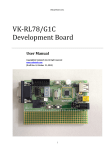
VK-RZ/A1H Development Board User manual Rev. 1.0, Dec.10.2014 Copyright(c) Vekatech Ltd, All right reserved INTRODUCTION VK-RZ/A1 is a starter kit which uses MCU R7S721000VCBG from Renesas Electronics. This powerful MCU is actually LSI, single-chip microcontroller that includes an ARM Cortex™-A9 processor along with the integrated peripheral functions required to configure a system. The core includes: 32-KB L1 instruction cache 32-KB L1 data cache 128-KB L2 cache. Integrated various on-chip peripheral functions and interfaces such as: 10-MB large-capacity RAM (128 KB are shared by the data-retention RAM) data-retention RAM multi-function timer pulse unit 2, OS timer, realtime clock motor control PWM timer UART, UART with FIFO, I2C, SPI, SPI multi I/O bus controller, CAN, LIN serial sound interface, sound generator, CD-ROM decoder A/D converter, SCUX media local bus, SD host interface, MMC host interface NAND flash memory controller IEBus™ controller, Renesas SPDIF interface Ethernet controller, EthernetAVB USB 2.0 host/function digital video decoder, video display controller 5 dynamic range compression, image renderer, image renderer for display display out comparison unit Renesas graphics processor for OpenVG™ JPEG codec unit, capture engine unit, pixel format converter interrupt controller modules, general I/O ports The kit supports: Ethernet, LVDS Port up to 128 MB SDRAM Mini SD card connector Composite video connector one USB ↔ UART converter two USB communication channels 20 pins JTAG programing and debugging interface All this along with the DC/DC power supply on board and connected to pin headers unused pins of R5F10KBC & R7S721000VCBG allow you to build a diversity of powerful applications to be used in a wide range of embedded tasks. BOARD FEATURES: MCU: RL78/G1C - R5F10KBC LSI: RZ/A1H - R7S721000VCBG USB Mini B device connector (RL78/G1C) 2xUSB Standard A device connectors (RZ/A1H) CAN connectors (Infineon TLE 6250) LVDS Port connector (RZ/A1H) Composite video connector (RZ/A1H) Micro SD card connector (RZ/A1H) SDRAM 64 MB (2x32MB) (RZ/A1H) Ethernet, RJ-45 10/100Mb MAC (RZ/A1H) PHY SMSC LAN8710A 20 pins Debug/programming connector (JTAG) 1 push RESET button Power connector for DC/DC 5V FR-4, 1.6 mm, Green/White solder mask, component print. Dimensions: 105.0mm x 74.0mm 1 ELECTROSTATIC WARNING The VK-RZ/A1H - R7S721000VCBG board is shipped in protective anti-static packaging. The board must not be subject to high electrostatic potentials. General practice for working with static sensitive devices should be applied when working with this board. PROCESSOR FEATURES The VK-RZ/A1H board use MCU R7S721000VCBG from RENESAS ELECTRONICS with these features: Power supply voltage: VDD = 3.0 to 3.6 V Operating ambient temperature: TA =−40 to +85°C Max. CPU clock (Iф) = 400 MHz) For more information please visit www.renesas.eu BLOCK DIAGRAM DC/DC Converter AP3512 Unused Pins 2x SPI flash 4bit I/O mode LVDS Port 1,18V USB Mini B Function CPU RL78/G1C R5F10KBC 5V USB <=> UART Unused Pins LSI RZ/A1H R7S721000VCBG UART ch: 3 Micro SD Card 2x USB Standard A Host / Function 2 E PROM 24C02 2 I C ch: 0 Composite video CAN ch: 1 RJ45 LAN 10-100 SMSC LAN8710A E1 Emulator CAN Infineon TLE6250 JTAG debuger SDRAM 32/64 MB A54C32W165A EXTERNAL SDRAM BASE ADDRESSES SDRAM SDRAM SDRAM SDRAM CS2: ORIGIN = 0x08000000, LENGTH = 64MB CS3: ORIGIN = 0x0C000000, LENGTH = 64MB CS2 mirror: ORIGIN = 0x48000000, LENGTH = 64MB CS3 mirror: ORIGIN = 0x4C000000, LENGTH = 64MB SDRAM is accessed with 16bit data width A14 & A15 are used for bank switching SCHEMATICS Please refer to CD for high quality pictures. 2 BOARD REFERENCE DESIGNATORS POWER SUPPLY CIRCUIT: VK-RZ/A1H is powered by (5) VDC applied at the power jack. VK-RZ/A1H could also be powered by USB Mini B connector. The consumption of VK-RZ/A1H may vary and the maximum is (@3.3V) 450mA. CLOCK CIRCUITS: Quartz Generator 13.3333 MHz is connected to EXTAL, pin# AA14. Quartz crystal 32.768KHz is connected to RTC_X1/RTC_X2, pins# AA7/Y7. Quartz crystal 4.0000MHz is connected to RTC_X3/RTC_X4, pins# V10/V11. Quartz crystal 48.0000MHz is connected to USB_X1/USB_X2, pins# A13/Y13. Quartz crystal 27.0000MHz is connected to VIDEO_X1/VIDEO_X2, pins# W21/V20. Quartz crystal 25.0000MHz is connected to Ethernet Phy - SMSC LAN8710A – (XTAL1/XTAL2 pins# 5/4). PUSH BUTTONS Button # SW1 Function Signal Name Pin# RESET U9 RESET JUMPERS CONFIGURATION Connected Disconnected 3 BOOT configuration: BOOT mode# JP4, JP5, JP6 Description 0 Boot from CS0 16 bit bus width 1 Boot from CS0 32 bit bus width Boot from SPI multi I/O ch0: [ P9_2 - P9_5 ] Boot from SD card ch0: [ P4_10 - P4_15 ] Boot from MMC card ch0: [ P5_10 - P5_15 ] 3 4 5 Clock settings: CLK mode# JP7, JP8 MD_CLK MD_CLK Description CLK source from EXTAL/crystal resonator CLK source from USB_X1/crystal resonator MD_CLKS SSCG circuit OFF MD_CLKS SSCG circuit ON JTAG Debugger settings: JTAG mode# JP9 Description 0 Normal operation 1 Boundary scan CAN Termination: CAN mode# JP3 Description 0 CAN line is terminated 1 CAN line terminated is not 4 EXTERNAL CONNECTORS DESCRIPTION PWR J1 Pin# Signal Name 1 +5V Pin# 2,3 Signal Name GND The power input should be +(5VDC) E1 Emulator 5pin connector E1 J17 Pin# 1 2 3 4 5 Signal Name GND TRESET RESET TOOL +5V JTAG 20pin connector JTAG J15 Pin# Signal Name 1 +3V3 3 TRST 5 TDI/JP0_0 7 TMS 9 TCK 11 13 TDO/JP0_1 15 SRST 17 19 - Pin# 2 4 6 8 10 12 14 16 18 20 Signal Name +3V3 GND GND GND GND GND GND GND GND GND CAN 3pin connector CAN J7 Pin# Signal Name 1 CAN_L 2 GND 3 CAN_H CTX1 is connected to P5_10 pin# A7 of R7S721000VCBG. CRX1 is connected to P5_9 pin# B7 of R7S721000VCBG. Termination Jumper JP3. Ethernet connector RJ45 type: J2 Transformer and integrated LEDS are connected/controlled to PHY interface LAN8710A. Respective signals from PHY are connected to MII interface of R7S721000VCBG. USB devices USB mini B J3 Pin# Signal Name 1 V_USB1 2 D- Pin# 3 5 Signal Name D+ GND Pin#4 ID is disconnected. V_USB1 Output USB device power. D- is connected to UDM0, pin#23 of R5F10KBC. D+ is connected to UDP0, pin#24 of R5F10KBC. 5 USB standard A J6 (lower) Pin# Signal Name Pin# 1 +5V 3 2 D4 Signal Name D+ GND USB standard A J6 (upper) Pin# Signal Name Pin# 5 +5V 7 6 D8 Signal Name D+ GND Both USB are configured as hosts ! lower D- is connected to DM0, pin#AA11 of R7S721000VCBG. lower D+ is connected to DP0, pin#Y11 of R7S721000VCBG. upper D- is connected to DM1, pin#AA9 of R7S721000VCBG upper D+ is connected to DP1, pin#Y9 of R7S721000VCBG Micro SD card slot: Micro SD J4 Pin# Signal Name MCU PIN# MCU PORT 1 DAT2 F18 P4_15/SD_D2_0 2 CD/DAT3 F17 P4_14/SD_D3_0 3 CMD G20 P4_13/SD_CMD_0 4 VDD 5 CLK H21 P4_12/SD_CLK_0 6 GND 7 DAT0 G18 P4_11/SD_D0_0 8 DAT1 H20 P4_10/SD_D1_0 9 NO-b 10 !CARDEXIST J21 P4_8/SD_CD_0 DAT0-3 (IN/OUT) - I/O Memory Card Interface Data 0-4. These are the data lines for the SD connector. They could be both input and output for the MCU depending on the data flow direction. CMD (OUT) - Output Memory Card Interface Command. This is a command sent form the processor to the memory card and as such it is output from the processor. CLK (OUT) - Output Memory Card Interface Clock. This signal is output from the MCU and synchronizes the data transfer between the memory card and the MCU. Composite video Composite video J16 Pin# Signal Name 1 V_USB1 Pin# 2 Signal Name D+ LVDS port connector: J8 The signals that are coming out from the connector ARE NOT DISPLAY PORT SIGNALS, regardless of the fact that the connector is the same. UNUSED PIN HEADERS PORT extension J5 (RL78/G1C) Pin# Signal Name 1 P16/TI01/TO01/INTP5 3 P17/TI02/TO02 P30/INTP3/SCK00/SCL00 5 /(TI03/TO03/PCLBUZ0) 7 P70/PCLBUZ1 9 P21/ANI1/AVREFM P01/ANI16/TO00/INTP9 11 /SCK01/SCL01/(SCLA0) 13 P62 15 P60/SCLA0 17 P122/X2/EXCLK 19 P121/X1 Pin# 2 4 Signal Name P31/TI03/TO03/INTP4/PCLBUZ0 P24/ANI4 6 P23/ANI3 8 10 P22/ANI2 P20/ANI0/AVREFP P00/ANI17/TI00/INTP8/SI01 /SDA01/(SDAA0) P120/ANI19/SO01/(PCLBUZ1) P61/SDAA0 P137/INTP0 GND 12 14 16 18 20 6 LCD extension J9 (RZ/A1H) Pin# Signal Name 1 P1_1/RIIC0SDA 3 P1_0/RIIC0SCL 5 P3_9/LCD0_DATA1 (B2) 7 P3_13/LCD0_DATA5 (G0) 9 P4_2/LCD0_DATA10 (G5) 11 P3_11/LCD0_DATA3 (B4) 13 P4_5/LCD0_DATA13 (R3) 15 P4_7/LCD0_DATA15 (R5) 17 P4_0/LCD0_DATA8 (G3) 19 P3_15/LCD0_DATA7 (G2) Pin# 2 4 6 8 10 12 14 16 18 20 Signal Name P3_0/LCD0_CLK P3_1/LCD0_TCON0 (DE) P3_8/LCD0_DATA0 (B1) P3_12/LCD0_DATA4 (B5) P3_14/LCD0_DATA6 (G1) P4_1/LCD0_DATA9 (G4) P4_4/LCD0_DATA12 (R2) P4_6/LCD0_DATA14 (R4) P3_10/LCD0_DATA2 (B3) P4_3/LCD0_DATA11 (R1) Pin# 2 4 6 8 10 12 14 16 18 20 Signal Name GND +3V3 P1_3/RIIC1SDA P1_6/RIIC3SCL P1_7/RIIC3SDA P3_7/LCD0_TCON6 (BKL_EN) P5_1/TXCLKOUTM P5_3/TXOUT2M P5_5/TXOUT1M P5_7/TXOUT0M J11 (RZ/A1H) Pin# Signal Name 1 P8_1/A9 3 P8_3/A11 5 P8_5/A13 7 P8_7/A15 9 P7_11/A3 11 P7_9/A1 13 P7_7/WE1/DQMLU 15 P7_5/RD/WR 17 P7_3/CAS 19 P7_1/CS3 Pin# 2 4 6 8 10 12 14 16 18 20 Signal Name P8_0/A8 P8_2/A10 P8_4/A12 P8_6/A14 P7_14/A6 P7_12/A4 P7_10/A2 P7_6/WE0/DQMLL P7_4/CKE P7_2/RAS J12 (RZ/A1H) Pin# Signal Name 1 P6_1/D1 3 P6_3/D3 5 P6_5/D5 7 P6_7/D7 9 P6_9/D9 11 P6_11/D11 13 P6_13/D13 15 P6_15/D15 17 P7_13/A5 19 P7_15/A7 Pin# 2 4 6 8 10 12 14 16 18 20 Signal Name P6_0/D0 P6_2/D2 P6_4/D4 P6_6/D6 P6_8/D8 P6_10/D10 P6_12/D12 P6_14/D14 P5_8/CS2 n.c Pin# 2 4 Signal Name +1V18 GND J10 (RZ/A1H) Pin# Signal Name 1 +5V 3 P1_4/RIIC2SCL 5 P1_2/RIIC1SCL 7 P1_5/RIIC2SDA 9 P3_2/LCD0_TCON1 (ON/OFF) 11 P7_8/LVDS_HPD 13 P5_0/TXCLKOUTP 15 P5_2/TXOUT2P 17 P5_4/TXOUT1P 19 P5_6/TXOUT0P SDRAM extension PORT extension J13 (RZ/A1H) Pin# Signal Name 1 +5V 3 +3V3 7 5 7 9 11 13 15 17 19 n.c n.c P1_9 n.c P1_12 P1_15 P5_10/CAN1TX P5_9/CAN1RX J14 (RZ/A1H) Pin# Signal Name 1 n.c 3 n.c 5 P8_10 7 P8_11 9 P8_13 11 P8_15 13 P9_1 15 n.c 17 RESET 19 GND 6 8 10 12 14 16 18 20 n.c n.c n.c P1_8 n.c P1_10 P1_11 P1_13 Pin# 2 4 6 8 10 12 14 16 18 20 Signal Name n.c n.c P8_8/TxD3 P8_9/RxD3 P8_12 P8_14 P9_0 +1V18 +3V3 +5V MECHANICAL DIMENSIONS: Dimensions are in mm [inch]. AVAILABLE DEMO SOFTWARE: 1 2 3 FREERTOS(TM) DEMO PROJECT PORTED FOR IAR AND BUILT FOR VK-RZ/A1H development board. CycloneTCP PROJECT PORTED FOR IAR AND BUILT FOR VK-RZ/A1H development board. u-boot, Linux PORTED FOR GCC AND BUILT FOR VK-RZ/A1H development board. 8