1
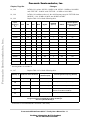
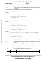
Freescale Semiconductor, Inc.
Errata to
MPC866UMAD
Rev. 1.4, 4/2004
Freescale Semiconductor, Inc...
Errata to the MPC866
PowerQUICC™ Family
User’s Manual Rev. 1.1
This errata describes corrections to Revision 1.1 of the MPC866 PowerQUICC™ User’s
Manual (order no. MPC866UM, Rev. 1.1). The MPC866 is a PowerPC™ architecture-based
derivative of Motorola’s MPC860 quad integrated communications controller
(PowerQUICC™). For convenience, the chapter number and page number of each erratum are
provided. Items in bold have been added since the last revision of this document.
To locate any published updates for
http://www.motorola.com/semiconductors.
1
this
errata,
refer
to
the
website
at
Document Revision History
Table 1 provides a revision history for this errata addendum.
Table 1. Document Revision History
Revision Number
Substantive Changes
1.1
Added new errata items from Chapter 14 (page 14-4, 14-6, 14-7, 14-22,
14-23), Chapter 30 (page 30-9), and Chapter 41 (page 41-6)
1.2
Added new errata items from Chapter 10 (page 10-6), Chapter 14 (page
14-16, 14-22, 14-23), Chapter 33 (page 33-18), Chapter 39 (page 39-6),
and Chapter 41 (page 41-5)
1.3
Added new errata items from Chapter 14 (page 14-1, 14-4), and Chapter
44 (page 44-23, 44-24, 44-37)
1.4
Added new erratum items from Chapter 21 (page 21-3), Ch 22 (page
22-1, 22-15), Appendix B (page B-4), Appendix H (page H-9)
For More Information On This Product,
Go to: www.freescale.com
Freescale Semiconductor, Inc.
Chapter, Page No.
2
Changes
Document Errata
The section and page numbers of new errata items added since the last errata addendum (03/15/04) are
boldfaced.
Freescale Semiconductor, Inc...
Section/Page
Changes
General erratum
Replace all instances of the term ‘60x’ with ‘external.’
10, 10-2
In the fourth bullet, the sentence ‘, thus providing a period from 122 µs to
8 seconds assuming a 32.768-kHz crystal,’ should be deleted.
10, 10-6
Add the following description for bit 19 in Table 3, “SIUMCR Field
Descriptions”:
Bit
Name
19
MPRE Multiprocessors reservation enable.
0 RSV/IRQ2 functions as IRQ2 and CR/IRQ3 functions as IRQ3.
1 RSV/IRQ2 functions as RSV. The interprocessor reservation protocol is enabled.
RSV functions as defined in Section 13.4.9, “Memory Reservation.”
10, 10-27
Description
In Section 10.10, the following text should be removed:
Solving this equation using a 32.768-kHz external clock gives
This gives a range from 122 µs (PITC = 0x0000) to 8 seconds
(PITC = 0xFFFF).
The equation in the middle of this text should also be deleted.
11, 11-3
Section 11.1.3.1 should be deleted.
11, 11-6
In Figure 11-3, bit 2 should be a ‘—’
11, 11-6
In Table 11-2, bit 2 should be a ‘—’, and in the description it should state
‘Reserved.’
12, 12-24
In Table 12-1, add a footnote reference to the ‘Hi-Z’ term next to every port pin.
The footnote should read:
14,14-1
During power-on reset all ports pins require at least 2 CLKOUT cycles
before they are three-stated. This means that until the DPLL locks and
CLKOUT is present for 2 cycles, the state of the port pins is undefined.
The first sentence in this page should be changed to: “The MPC866 clock system
provides many different clocking options for all on-chip and external devices.”
14, 14-1
The fourth sentence in this page should be changed to: “Also, to enable flexible
power control, the MPC866 provides frequency divider options.”
14, 14-4
The last two sentences in the sencond paragraph should be changed to: “Three of
these modes require a 10 MHz to 10.66 MHz input frequency, while the fourth
mode can accept from 45 MHz to 66 MHz. After reset, the PLPRCR can be
programmed to achieve a different general system clock as long as the following
requirements are met:
• OSCM is 10 MHz to 10.66 MHz (MODCK = 00 or 01)
• EXTCLK is 10 MHz to 10.66 MHz (MODCK = 11)
• EXTCLK is 45 MHz to 66 MHz (MODCK = 10)”
Errata to the MPC866 PowerQUICC™ Family User’s Manual Rev. 1.1
For More Information On This Product,
Go to: www.freescale.com
Freescale Semiconductor, Inc.
Chapter, Page No.
14, 14-4
In Table 14-1, replace ‘OSCM = 10 MHz’ with ‘OSCM = 10 MHz to 10.66 MHz’
and ‘EXTCLK = 10 MHz’ with ‘EXTCLK = 10 MHz to 10.66 MHz’.
14, 14-4
In Table 14-1 and the text above it, the valid frequency range for EXTCLK when
MODCK = 10 is 45 MHz–66 MHz, not 40 MHz–66 MHz.
14, 14-6
Replace Table 14-2 with the following table:
Input
Frequency
(fref)
Freescale Semiconductor, Inc...
Changes
1
2
General System
Frequency (MHz)
[GCLK2] 2
MFD
dpgdck
PLPRCR
S[10:11]
0
0
160
1
80
40
9
6
9
192
1
96
48
0
10
4
9
208
1
104
52
10 MHz
0
13
2
9
264
1
132
66
10 MHz
0
15
0
0
300
1
150
75
10 MHz
0
10
0
0
200
0
200
100
10 MHz
0
13
3
9
266
0
266
133
45 MHz
3
8
0
0
180
1
90
45
45 MHz
2
8
1
2
250
0
250
125
50 MHz
2
9
0
0
300
1
150
75
50 MHz
1
5
2
6
264
0
264
132
66 MHz
2
6
0
1
264
1
132
66
66 MHz
2
6
0
1
264
0
264
132
PDF
MFI
10 MHz
0
8
10 MHz
0
10 MHz
MFN
1
JDBCK
For MFN = 0, EXTCLK will be synchronized to CLKOUT.
Assuming DFNH = 0 and CSR = 0.
14, 14-7
MODCK[1–2]
Replace Table 14-3 with the following table:
Default at Power-On Reset
OSCLK (DPLL and
Interface Input)
General System Frequency (GCLK2)
MFI[12–15]
PDF[27–30]
00
8
0000
OSCM freq
40 MHz (for OSCLK freq = 10 MHz)
01
15
0000
OSCM freq
75 MHz (for OSCLK freq = 10 MHz)
10 1
6
0010
EXTCLK freq
1:1 mode (The allowable frequencies on
EXTCLK are 45 MHz to 66 MHz)
11
15
0000
EXTCLK freq
75 MHz (for EXTCLK freq = 10 MHz)
Note: S = 1, MFN = 0, and MFD = 1 for all of the reset configurations.
The general system clock[GCLK2] is jdbck divided by 2.
divout1 is jdbck divided by 2.
1
For Revision 0.x of the MPC866, MFI = 8 and PDF = 0011 binary.
Errata to the MPC866 PowerQUICC™ Family User’s Manual Rev. 1.1
For More Information On This Product,
Go to: www.freescale.com
Freescale Semiconductor, Inc.
Chapter, Page No.
Changes
14, 14-12
In Figures 14-7 and 14-8, CLKOUT should be identical to GCLK2_50.
14, 14-16
In Table 14-16, change the title of the third column from ‘MF’ to ‘MFI/(PDF+1)’.
14, 14-18
The value of the inductor described in the last sentence of the first paragraph
should be 8.2 milli-Henry (mH).
14, 14-22
In Figure 14-13, replace the ‘0000’ under field PDF with ‘—’ because PDF is not
affected by HRESET.
14, 14-22
In Figure 14-13, change the name of bit 26 from ‘FIOPD’ to ‘—’.
14, 14-23
In Table 14-9, add the following description for bit 26:
Bit 26 —Reserved, should be cleared.
Freescale Semiconductor, Inc...
18, 18-14
After Table 18-10, add the following note:
NOTE
Operating serial ATM or Ethernet on SCC1-4, or the UTOPIA interface on
SCC4 causes other peripherals to lose their parameter RAM. For example,
for SCC1, the serial ATM parameters extend into the I2C parameter RAM
default location. Likewise for SCC2, the serial ATM parameters extend
into the SPI parameter RAM. However, the parameters for both SPI and
I2C can be relocated without the need for RAM-based microcode. The
parameter RAM for SCC3/SMC1 and SCC4/SMC2/PIP is affected in the
same manner and can be relocated using a RAM microcode patch available
on the Motorola website www.mot.com/netcomm.
21, 21-3
The third bullet should read:
Additional protocols supported through Motorola-supplied RAM
microcodes: Signaling System #7 (SS7), ATM over T1/E1 (ATOM1)
21, 21-10
The following is the correct description for MODE in Table 21-3, which
describes GSMR_L fields:
Table 21-3. GSMR_L Field Descriptions
Bits
28–31
Name
Description
MODE Channel protocol mode. See also GSMR_H[TTX, TRX].
0000 HDLC
0001 Reserved
0010 AppleTalk/LocalTalk
0011 SS7—reserved for RAM microcode
0100 UART
0101 Reserved
0110 Asynchronous HDLC or IrDA
0111 Reserved
1000 BISYNC
1001 Reserved
101x Reserved
1100 Ethernet
All others reserved
21, 21-22
In Figure 21-13, the top input to the NOR gate should be RENC ‘not equal to’
NRZI.
22, 22-1
The last sentence in the last paragraph should be removed.
Errata to the MPC866 PowerQUICC™ Family User’s Manual Rev. 1.1
For More Information On This Product,
Go to: www.freescale.com
Freescale Semiconductor, Inc.
Chapter, Page No.
Changes
22, 22-15
In the RZS field (bit 7) of Table 22-9, for selection 1, the second sentence in
the paragraph (making reference to V.14 applications) should be removed.
30, 30-9
The SPI examples with different SPMODE[LEN] values are incorrect. It should
be as follows:
For all examples below, assume the memory contains the following binary image:
msb ghij_klmn__opqr_stuv
Example 1
with LEN = 0x4 (data size = 5), the following data is selected:
msb xxxj_klmn_xxxr_stuv
with REV=0, the string transmitted is:
Freescale Semiconductor, Inc...
first nmlk_j__vuts_r
with REV=1, the string transmitted is:
first j_nmlk__r_stuv
Example 2
with LEN = 0x7 (data size = 8), the following data is selected:
msb ghij_klmn_opqr_stuv
with REV=0, the string transmitted is:
first nmlk_jihg__vuts_rqpo
with REV=1, the string transmitted is:
first ghij_klmn__opqr_stuv
Example 3
with LEN = 0xc (data size = 13), the following data is selected:
msb ghij_klmn_xxxr_stuv
with REV=0, the string transmitted is:
first nmlk_jihg__vuts_r
with REV=1, the string transmitted is:
first r_stuv__ghij_klmn
32, 32-11
In Table 32-8, bits 0–7 correspond to TPAR2, and bits 8–15 correspond to TPAR1
33, 33-2
Delete the sixth bullet from the top and add the following note at the end of the
feature list:
NOTE
During power-on reset, all port pins require at least 2 CLKOUT cycles
before they are three-stated. This means that until the DPLL locks and
CLKOUT is present for 2 cycles, the state of the port pins is undefined.
33, 33-8
Pins PB20 and PB21 should to be added to Table 33-6.
PB21
Port B21
SMTXD2
L1CLKOB
—
PB20
Port B20
SMRXD2
L1CLKOA
SMRXD2 = GND
Errata to the MPC866 PowerQUICC™ Family User’s Manual Rev. 1.1
For More Information On This Product,
Go to: www.freescale.com
Freescale Semiconductor, Inc.
Chapter, Page No.
Changes
33, 33-18
In Table 33-18, the column titled ‘UT=1’ should be renamed to ‘UT=1 master’.
Also, add another column next to ‘UT=1 master’ titled ‘UT=1 slave’. This new
column should contain the UTOPIA signals as shown in Figure 42-2.
33, 33-18
Add the following description for Port D data direction register (PDDIR):
33.5.1.2 Port D Data Direction Register (PDDIR)
The port D data direction register (PDDIR) provides bits for specifying whether
port D signals are inputs or outputs when functioning as general-purpose I/O. It
is also used to specify whether PD8 and PD10 function as open-drain pins.
0
1
Freescale Semiconductor, Inc...
Field OD8 OD10
Reset
2
—
3
4
5
6
7
8
9
10
11
12
13
14
15
DR3 DR4 DR5 DR6 DR7 DR8 DR9 DR10 DR11 DR12 DR13 DR14 DR15
xxxx_xx00_0000_0000
R/W
R/W
Addr
0x970
Figure 33-17. Port D Data Direction Register (PDDIR)
This register is affected by HRESET but is not affected by SRESET. Table 33-20
describes the PDDIR bits.
Table 33-20. PDDIR Bit Descriptions
Bits
Name
0–1
ODn
2
—
3–15
DRn
Description
Specifies the open-drain functionality of PD8 or PD10 as follows:
0 The I/O pin is actively driven as an output
1 The I/O pin is an open-drain driver. As an output, the pin is actively driven low. Otherwise, it is
three-stated.
Reserved and should be cleared.
Port D data direction. Configures port D signals as inputs or outputs when functioning as
general-purpose I/O.
0 The corresponding signal is an input.
1 The corresponding signal is an output.
39, 39-6
In Section 39.1.4, replace the two instances of ‘CLKOUT’ with ‘General System
Clock’.
39, 39-7
Add the following note:
NOTE
When using AAL5 VBR for transmit, after AAL5 Tx under run situation
(UN bit is set in Interrupt Queue Entry), if the software makes the AAL5
Tx BD ready again (set TxBD[R] bit), the immediate pace between the
first and second cell of this AAL5 frame becomes OOBR, which should be
PCR according to VBR algorithm. To solve this Tx underrun situation,
right before setting TxBD[R] bit, software should first clear the BNR bit
in the TCT. Then the immediate pace between the first and second cell of
this AAL5 frame will be PCR.
Errata to the MPC866 PowerQUICC™ Family User’s Manual Rev. 1.1
For More Information On This Product,
Go to: www.freescale.com
Freescale Semiconductor, Inc.
Chapter, Page No.
41, 41-6
Changes
Add the following footnote at the bottom of Table 41-5 in reference to pin
assignment for TXD4 on pin PD8:
‘Available only when UTMODE[SPLIT]=0’
41, 41-5
In Table 41-5 the column titled ‘UT=1’ should be renamed to ‘UT=1 master’.
Also, add another column next to ‘UT=1 master’ titled ‘UT=1 slave’, this new
column should contain the UTOPIA signals as shown in Figure 42-2.
42, 42-1
The third bullet from the top should read:
• Supports external or internal UTOPIA clock up to 33 MHz in both master and
slave mode (receive and transmit).
In Section 44.4.1.11, the third sentence in the second paragraph should be
changed to: “Once an RxBD whose E bit is cleared is polled, the
R_DES_ACTIVE bit is cleared and polling stops until the user sets the
R_DES_ACTIVE bit again, signifying additional RxBDs have been placed into
the RxBD ring”.
Freescale Semiconductor, Inc...
44, 44-23
44, 44-24
In Section 44.4.1.12, the third sentence in the second paragraph should be
changed to: “Once a TxBD whose R bit is cleared is polled, the X_DES_ACTIVE
bit is cleared and polling stops until the user sets the X_DES_ACTIVE bit again,
signifying additional TxBDs have been placed into the TxBD ring”.
44, 44-37
In Table 44-35, the description for bit 1 (RO1) should be changed to: “Receive
software ownership bit. Software use. This read/write bit is not modified by
hardware and does not affect hardware”.
Appendix B, B-4
In Table B-1, the row that makes a reference to SCC in Profibus should be
removed.
Appendix F, F-1
Add the following to the MPC859T feature list:
— Up to only 32 independent communication channels
— Arbitrary mapping of any of 32–63 channels to any of 32–63 TDM time slots
Appendix H, H-9
In Table H-4, it is stated that ‘OP3/MODCK2/DSDO is acting as DSDI while
DBPC is equal to 11.’ It should read DSDO, not DSDI.
Appendix H, H-9
In Table H-4, the descriptions under the DBPC = 11 column should all be
‘Reserved’.
Appendix H, H-9
In Table H-4, the descriptions under the DBPC = 00 and 11 columns for the
DSCK row should both be ‘Reserved’.
Appendix H, H-9
In Table H-4, the descriptions under the DBPC = 00 and 11 columns for the
OP3/MODCK2/DSDO row should both be ‘Defined by DBGC’.
Errata to the MPC866 PowerQUICC™ Family User’s Manual Rev. 1.1
For More Information On This Product,
Go to: www.freescale.com
Freescale Semiconductor, Inc...
Freescale Semiconductor, Inc.
Home Page:
www.freescale.com
email:
[email protected]
USA/Europe or Locations Not Listed:
Freescale Semiconductor
Technical Information Center, CH370
1300 N. Alma School Road
Chandler, Arizona 85224
(800) 521-6274
480-768-2130
[email protected]
Europe, Middle East, and Africa:
Freescale Halbleiter Deutschland GmbH
Technical Information Center
Schatzbogen 7
81829 Muenchen, Germany
+44 1296 380 456 (English)
+46 8 52200080 (English)
+49 89 92103 559 (German)
+33 1 69 35 48 48 (French)
[email protected]
Japan:
Freescale Semiconductor Japan Ltd.
Headquarters
ARCO Tower 15F
1-8-1, Shimo-Meguro, Meguro-ku
Tokyo 153-0064, Japan
0120 191014
+81 2666 8080
[email protected]
Asia/Pacific:
Freescale Semiconductor Hong Kong Ltd.
Technical Information Center
2 Dai King Street
Tai Po Industrial Estate,
Tai Po, N.T., Hong Kong
+800 2666 8080
[email protected]
For Literature Requests Only:
Freescale Semiconductor
Literature Distribution Center
P.O. Box 5405
Denver, Colorado 80217
(800) 441-2447
303-675-2140
Fax: 303-675-2150
LDCForFreescaleSemiconductor
@hibbertgroup.com
Information in this document is provided solely to enable system and software
implementers to use Freescale Semiconductor products. There are no express or
implied copyright licenses granted hereunder to design or fabricate any integrated
circuits or integrated circuits based on the information in this document.
Freescale Semiconductor reserves the right to make changes without further notice to
any products herein. Freescale Semiconductor makes no warranty, representation or
guarantee regarding the suitability of its products for any particular purpose, nor does
Freescale Semiconductor assume any liability arising out of the application or use of
any product or circuit, and specifically disclaims any and all liability, including without
limitation consequential or incidental damages. “Typical” parameters which may be
provided in Freescale Semiconductor data sheets and/or specifications can and do
vary in different applications and actual performance may vary over time. All operating
parameters, including “Typicals” must be validated for each customer application by
customer’s technical experts. Freescale Semiconductor does not convey any license
under its patent rights nor the rights of others. Freescale Semiconductor products are
not designed, intended, or authorized for use as components in systems intended for
surgical implant into the body, or other applications intended to support or sustain life,
or for any other application in which the failure of the Freescale Semiconductor product
could create a situation where personal injury or death may occur. Should Buyer
purchase or use Freescale Semiconductor products for any such unintended or
unauthorized application, Buyer shall indemnify and hold Freescale Semiconductor
and its officers, employees, subsidiaries, affiliates, and distributors harmless against all
claims, costs, damages, and expenses, and reasonable attorney fees arising out of,
directly or indirectly, any claim of personal injury or death associated with such
unintended or unauthorized use, even if such claim alleges that Freescale
Semiconductor was negligent regarding the design or manufacture of the part.
For More Information On This Product,
Go to: www.freescale.com