1
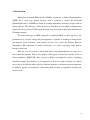
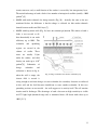
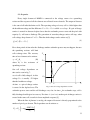
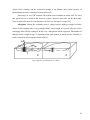
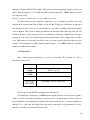
VILNIUS UNIVERSITY FACULTY OF PHYSICS SEMICONDUCTOR PHYSICS DEPARTMENT Vytautas Vislavičius ANALYSIS OF SILICON PHOTOMULTIPLIER RESPONSE Bachelor Thesis (Study Program – APPLIED PHYSICS) Student Vytautas Vislavičius Supervisor RNDr. PhD. Peter Kodyš Reviewer Habil. Dr. Eugenijus Gaubas Consultant Head of Department Dr. Vincas Tamošiūnas Prof. Habil. Dr. Gintautas Tamulaitis Experimental part of work was done in the Institute of Particle and Nuclear Physics, Faculty of Mathematics and Physics, Charles University in Prague, Czech Republic. Prague/Vilnius, 2011 I declare that I wrote my bachelor thesis independantly and exclusively with the use of cited sources. I agree with lending and publishing the thesis. Pripažįstu, kad šį darbą parašiau pats nepriklausomai, naudodamasis paminėtais literatūros šaltiniais. Sutinku, kad šis darbas būtų publikuojamas ar naudojamas kaip literatūros šaltinis. Vytautas Vislavičius Prague/Vilnius, 26 May, 2011 2 Table of contents 1. Introduction ................................................................................................................................. 4 2. Semiconductor detectors ............................................................................................................. 5 2.1. Semiconductor detector model ............................................................................................. 5 2.2. Three types of MAPD......................................................................................................... 10 2.3. Properties ............................................................................................................................ 13 2.4. Noise................................................................................................................................... 15 3. MAPD-S60 response analysis ................................................................................................... 17 3.1. Measurement schematics.................................................................................................... 17 3.2. Measurements description .................................................................................................. 18 3.3. Data analysis....................................................................................................................... 19 3.4. Results ................................................................................................................................ 27 4. Conclusions ............................................................................................................................... 35 5. References.................................................................................................................................. 36 6. Appendix .................................................................................................................................... 37 6.1. Data analysis software ........................................................................................................ 37 7. Summary .................................................................................................................................... 40 3 1. Introduction Micro-pixel Avalanche Photo Diodes (MAPD), also known as Silicon Photomultipliers (SiPM) are a novel type photon detectors with a potential to replace the traditional photomultiplier tubes. A MAPD is a matrix of avalanche photodiodes working in Geiger mode on silicon substrate. The efficiency of these detectors is dependant on wavelength of photon being registered and is greatest in UV-IR region, therefore, they are usually coupled with scintillators or Cherenkov counters. The main advantages of SiPM, compared to traditional PMTs, are their rigid size, low production costs, low bias voltage and most important – capability of working in strong electric and magnetic fields. Therefore, such detectors can be used in areas like Positron Emission Tomography, EM calorimetry in particle accelerators, etc., where registering single photons becomes a main task. However, a lot of research is still needed before such photomultipliers are ready to be used at their full potential. Thus it is the purpose of this paper to analyze the response of one of silicon multipliers, MAPD-S60, when exposed to 682nm wavelength laser pulses, simulating scintillators output. In particular, it is of importance to check its response linearity over surface area as well as its behavior when exposed to different intensities of radiation and, most important, its ability to register several photons, when timing between them is comparable with detectors recovery time. 4 2. Semiconductor detectors Some general requirements have to be met when choosing a material for a semiconductor detector for electromagnetic radiation. In particular, the material is required to be as dense as possible, so the interaction cross-section of initial radiation with matter is high. On one hand, excitation energy of atoms in matter has to be low so there are more charge carriers created; on the other hand, low excitation energy results in a higher number of thermal charge carriers. To achieve good time characteristics, mobility of charge carriers in matter has to be high so they are collected before they can recombine. So far the best materials fulfilling these requirements are germanium and silicon. [1] 2.1. Semiconductor detector model Operating principle Energy levels of atoms in a solid state body combine to make energy bands. The highest filled energy band is called valance band and the one above it – conductive band; the gap between those two is energy gap (fig. 1a). Electrons in valance band are bound to atoms; however, provided sufficient energy, they can transit to conductivity band, where they are free to move and drift along the electric field. When temperature is above 0K, a fraction of all the atoms is already excited and there are some electrons in conductivity band already. In such case, width of energy gap is of great importance, since it influences the initial amount of free charge carriers.[1] In case of intrinsic semiconductor, number of initial free charge – carriers is small, thus to increase it, impurities are introduced. Also called dopants, they can be of two types: donor or acceptor. Impurities create discrete energy levels in the energy gap of intrinsic semiconductor and these levels are close to either valance or conductivity band. Donor type impurities (donors) create an energy level just below the conductivity band and therefore they can easily ionize (fig. 1b). In such a case donor remains stationary in crystal lattice, while the electron enters the conductivity band and becomes free. Similarly, acceptor type impurities (acceptors) create discrete energy levels just above valance band and thus can ionize an intrinsic atom (fig. 1c). Such a case results in a generation of a positively charged free quasi-particle - a hole - which is also free to move. If the concentration of donors is higher than the one of acceptors, a 5 semiconductor is called n – type semiconductor and its majority carriers are electrons. In opposite case where the concentration of acceptors is higher than the one of donors, a semiconductor is called p – type semiconductor and its majority carriers are holes.[1]. a) Intrinsic semiconductor b) n – type semiconductor c) p – type semiconductor Fig. 1: Energy level diagrams for a) intrinsic, b) n – type, c) p – type semiconductors When two different conductivity semiconductors (or same conductivity semiconductors with different concentration of impurities) are joined together, a pn diode is created. Because of a higher concentration of holes in p region, they start to diffuse to n region. Similarly, electrons from n region diffuse to p region. This effect results in imbalanced volume charges in both p and n parts of diode, creating an electric field. It is because of this field that charge carriers start moving in directions, opposite to the (a) ones caused by diffusion – this movement is called drift. Finally, drift and diffusion currents compensate each other – diode comes to equilibrium and a potential difference UK (b) in junction is created. Concentrations of electrons and holes, ionized impurities concentrations and volume charges distributions dependance on coordinate is shown in (c) figures 2 a, b and c respectively.[1] Because of this field, charge carriers gain potential energy, thus their conductivity and valance bands shift and can be written as: E c = E c 0 − eϕ E v = E v 0 − eϕ (1) Fig. 2: a) Concentration of e- and h+, b) concentration of ionized impurities and c) volume charges distribution dependance on coordinate, when pn junction is in equilibrium 6 E (a) U0 = 0 E Ec n (b) U0 < 0 n Ec e0(Uk - U0) e0Uk Ev Ev e0Uk p e0(Uk - U0) p x x Fig. 3: Energy levels of pn junction when a) no external voltage is applied, b) external reverse voltage is applied Since φ is dependant on coordinate, energy levels also become dependant on coordinate. Moreover, because of differences in potentials in junction, charges moving from one side of diode to another have to overcome potential barrier e0UK (Fig. 3). Applying external voltage, this barrier can be either increased or decreased.[1] In the region of volume charge, concentration of free charge carriers is dramatically lower than in neutral areas; therefore, resistance in this region is much higher than in neutral one. In such a case all the electric field falls in this high – resistance zone, which is called depleted zone. Thickness of depleted zone can be expressed as: d= 2εε 0 (N A + N D ) (U K − U 0 ) eN A N D (2) where NA stands for acceptor concentration, ND – donor concentration, UK – potential of junction, U0 – external voltage (U0 > 0 if direct biased, U0 < 0 if reverse biased), ε and ε0 – dielectric permeability in matter and vacuum respectively. Usually, concentration of some type of impurities is much bigger than of the other type, moreover, U 0 >> U K (in case of reverse biased). Then (2) can be simplified to: d= 2εε 0 U0 eN X (3) 7 where NX – lower concentration of impurities. Depleted zone is the active area of pn detector, where the incident particles create e- - h+ pairs, which are later collected by corresponding electrodes and thus create a signal.[1] A diode with a depleted zone of area S and thickness D operates like a planar capacitor with capacity: C= εS D = εε 0 eN X 2U 0 (4) To achieve a better energy resolution, capacity has to be reduced, thus the external voltage has to be increased.[3] Leakage currents Even if the detector is not exposed to any radiation, a small current (< 1µA) will be registered if detector is reverse biased. This current can be both volume- and surface- type. There are two sources for volume leakage currents: • Minority charge carriers in p and n regions, having diffused from neutral to depleted zone, will be exposed to electric field and will drift to the corresponding part of diode. Since these charges are continuously generated in both sides of junction and are free to diffuse, a small constant current will be registered. Usually generation of such carriers is small and do not have much influence on signal registered. • Another source for leakage current is thermal pair generation in depleted zone. Apparently number of such charges will grow with increasing thickness of depleted region; therefore to avoid this detector has to be constantly cooled. For silicon such a generation in room temperature is small; on the other hand, germanium has to be constantly cooled by liquid nitrogen, for its energy gap width is narrow.[3] Surface leakage currents originate on the surface of detector nearby the junction where potential barrier is big. These currents are influenced by many factors, such as humidity, dirty surface and basically anything, that could change conductivity on surface.[3] Leakage currents not only influence detectors energy resolution, but also reduce U0. To isolate signal, reversed voltage is usually applied via series of resistors. Thus, U0 then becomes: U 0 → U 0 − il RQ (5) where il stands for leakage current and RQ – resistance of all the resistors connected to detector.[3] 8 Avalanche amplification Internal amplification processes in previously described detector do not occur. Therefore, even having the noise reduced to the minimum, it is impossible to identify one photon response using just external amplifiers. In such case, avalanche effect can be exploited: in very strong electric fields (~200keV/cm), charge carriers can be accelerated to energies sufficient to ionize other atoms of lattice via collisions (process is called impact Newly ionization). created electric particles can also be accelerated to sufficient energies to ionize even more atoms. As a result, the signal can be amplified up to measurable values. Ionization coefficient α is written: α= (6) N e−h l where Ne-h – number of e- - h+ pairs created by initial charge carriers, l – drift path. Typical MAPD ionization coefficient Fig. 4: typical MAPD ionization coefficient dependance on applied electric field.[2] α = f (1/E) is shown in figure 4.[4] Because of their low mobility, holes create much less free charges, therefore αh < αe and process can be classified into two modes: • Proportional mode: in relatively low electric fields αh << αe, therefore we can neglect the secondary charges generated by holes. Average number of impact ionization events caused by a single photon can be n = N0eαL written as: (7) where L is mean drift path. It is apparent from this expression that the response signal is dependant on N0 – initial photoelectrons. Gain factor in such case is:[2] G= n N0 =eαL (8) 9 • Geiger mode: in stronger electric fields holes must also be accounted for. They create electrons nearby the edge of depleted layer which later drift through the entire zone and extend the avalanche. Process continues until the external resistors suspend it. The charge created in such a case is not influenced by the number of initial photoelectrons, but rather by capacity of junction and current suppression mechanism. Should such a detector be exploited improperly, i.e. the avalanche is not suppressed, the detector would suffer irreversible damage.[2] Avalanche photodiodes are used to register a low intensity light. Usually they operate in proportional mode, however, if so, external amplifiers are still needed, for gain is not large enough to distinguish between signal and noise. The disadvantages of a detector working in proportional mode are following: • Gain dependance on temperature • Gain dependance on bias voltage • Insufficient signal discrimination [2] To overcome the last problem, detector should be used in Geiger’s mode. Then single photon registration efficiency would increase dramatically; however, the diode would only be usable with low intensity radiation. In order to extend its dynamic range, a number of avalanche photodiodes (APDs) can be joined together into one single matrix.[2] 2.2. Three types of MAPD Micro-pixel Avalanche Photodiode (MAPD) is basically a number of ordinary avalanche photodiodes joined into a single matrix. Each of APD, all connected to a single common electrode, is working in Geiger’s mode. The realization of APDs matrix, however, is not unambiguous – various models of such a detector yield different parameters. Currently, there are three types of MAPD (Fig. 5) [5]: • MAPD with individual surface resistors (Fig. 5a) consists of pn junctions on the surface. These junctions are connected to a common electrode via individual quenching resistors, which are seperated from silicon wafer by a layer of SiO2.[6] High resistivity resistors limit the avalanche processes and discharge the cells to a common electrode. This type of MAPD are sensitive to UV light. Big gaps between each cell result in small probability of short10 circuit, moreover, only a small fraction of the surface is covered by low-transparency layer. The main disadvantage of such a diode is low number of micropixels availabe (usually ~1000 px/mm2).[5] • MAPD with surface channels for charge transfer (Fig. 5b) – basically the same as the one mentioned before, the difference is that the charge is collected via thin surface channels formed between waffer and SiO2 layer [7]. • MAPD with deep micro-wells (Fig. 5c) have one common pn junction. The surface of such a diode is not covered at all, thus theoretically it can reach efficiency up to 100%. The avalanche and quenching regions are created in the volume zones of are waffer. These usually 3-5µm under the surface, and their density can reach up to 4·104 px/mm2[8]. charge Schematics avalanche of and collection is shown in fig. 6: when the well is empty, the Fig. 6. Charge avalanche and collection schematics[13] electric field it created is strong enough to accelerate charges to cause avalanche; the secondary electrons are collected in this well and the field becomes insufficient to cause another avalanche. In this case quenching resistors are not needed – the well suppresses its activity itself. The cell remains inactive until it discharges. The advantages of such a detector are high sensitivity to visible and UV light, high dynamical range and, as mentioned above, fill factor with values up to 100% [5,13] 11 Fig. 5: Schematic views of three MAPD types: (a) MAPD with individual surface resistors; (b) MAPD with surface transfer of charge carriers; (c) MAPD with individual micro-wells. 1—Common metal electrode, 2— buffer layer of silicon oxide, 3—p–n junctions/micro-pixels, 4—individual surface resistors, 5—individual surface channels for the transfer of charge carriers, 6—drain region/contact, 7—epitaxial silicon layer of p-type conductivity, 8—a high-doped silicon layer of p-type conductivity, 9—a region with micro-wells, 10—local avalanche regions, 11—individual micro-wells.[5] 12 2.3. Properties Every single element of MAPD is connected to the voltage source via a quenching resistor and the response of all the elements are collected in one electrode. The output of detector is the sum of all individual micro cells. The operating voltage of every cell is a little higher than the breakdown voltage and the difference Uov= Ubias - Ubd is called overvoltage. If a pair of charge carriers is created in detectors depleted area, then the avalanche process starts and the pixel with capacity Cpx will start to discharge. The generation of secondary charge carriers will stop, when cells voltage drops down to U < Ubd. Then the whole charge can be written as:[2] Q = C px (U bias − U bd ) (9) For a short period of time after the discharge another avalanche process may not happen, because the quenching resistors will limit cells recharge time. The recovery Umc time of one element can be written: τ r = C px Rq (10) Ubias where Rq is the resistance of quenching resistor. One cell voltage dependance on time can be seen in fig. 7: at t=0 cell is fully charged, its bias Ubd voltage Ubias is usually ~3V higher than the breakdown voltage. At time τ1 a pair of charge carriers τ1 τ2 τ3 t Fig. 7: One cell voltage dependance on time is created in the depleted area. The avalanche process starts and the cell discharges very fast. At time τ2 the avalanche stops, cell is fully discharged and begins its recovery. If at time τ* (τ2<τ*<τ3) another pair of charge carriers is created in the same cell, it results in lower amplitude response.[9] When the flux of photons is not big, the output of detector is directly proportional to the number of pixels per detector. The dependance can be written as: − PDE ⋅ N ph N f = N px 1 − exp N px (11) 13 where Npx stands for number of pixels in matrix, Nph – number of photons hit the detector, PDE – photodetection efficiency. Even this expression fails when the length of pulse is longer than detectors recovery time.[2] Gain The gain can be written as G= (U −U bd ) Q = C px bias e0 e0 (12) From this equation we can see that G can be increased whether with increasing capacitance, bias voltage or breakdown voltage.[3] Bias voltage Ubias Adjusting this parameter is the easiest way to adjust the gain coefficient. It can be shown, that G= εε 0 N X (U bias − U bd ) 2e0 U bias = εε 0 N X 2e0 U bias − U bd U bias (13) If the capacitance is 50pF, Ubd = 57 V, Ubias = 60 V, then we have G ≈ 1.2·105. However, with increasing bias voltage the influence of some side effects is also increased.[9] Breakdown voltage Ubd. This parameter is dependant on temperature; the dependance coefficient is negative, usually in range of 10-100 mV/K.[9] Ubd dependance on temperature can be analyzed as electrons scattered by phonons. Energy gained by a charge carrier in electric field is proportional to its free path along the direction of field. This energy has to be higher that the width of energy gap, so the atom can be ionized. If the length of free path is limited by phonons, then it can be written as λ = λ0 (2 N + 1)−1 , where λ0 – free path in T=0K, N - phase space of phonons. The later can be expressed as [10,11] hν N = exp q − 1 kbT −1 (14) 14 where νq stands for the effective energy of phonons in scattering. Then the breakdown voltage can be written Eg d U bd = (2 N + 1) e0λ0 (15) where Eg stands for energy gap width and d – depleted layer thickness. Photodetection efficiency PDE can be expressed in 4 terms [2,9]: PDE = Q.E . ⋅ ε pav ⋅ ε pl ⋅ ε Geig • (16) εpav – fill factor – becouse of electronics, not all the surface of detector is active: photons hitting the inactive areas will not be registered. • εpl – permeability factor – photons reflected from surface or absorbed in dead layer will not be detected • Q.E. – quantum efficiency – the ratio of photons that created a pair of charge carriers to the ratio of photons that got into active area • εGeig – probability for a charge carrier to start avalanche process. 2.4. Noise Every single charge carrier to get into avalanche region creates a signal same as incident photon. Such a signal generated by thermal charge carriers is usually in range of 100kHz up to few MHz per mm2. There are few ways to reduce the noise:[9] • Cooling the detector – number of carriers decreases by a factor of 2 for every 8K • Reducing the charge colection area • Reducing the Ubias – gain also reduces Apart from termal noise, there are some other unwanted effects:[9] • Optical cross-talk • Afterpulses Optical cross-talk is the effect when one charge carrier escapes from a cell and is cought in another cell, where it starts another avalache process (Fig.8). On the other hand, in strong 15 electric fields electrons can be accelerated enough so the photons they radiate becouse of bremstralung can cause avalanches in other micro-cells. On average, in every 106 electrons, 30 of them create avalanche in nearby cells. To avoid this, pixels have to be isolated; this, however, reduces detectors active area; on the other hand, lower electric fields mean less acceleration as well as less electrons to escape.[2,9] Afterpulses. During the avalanche process, charge carriers might get trapped in lattice defects. If the trapping time is long enough, charge carrier might be released when the cell is recharging or has already recharged. In this case, a fake photon will be registered. The number of charged carriers cought in traps is dependant of the total number of charge carriers, therefore, it can be reduced by decreasing the electric field.[9] Fig.8: Optical cross-talk between two cells[9] 16 3. MAPD-S60 response analysis 3.1. Measurement schematics Measurement schematics are shown in figure 9. Fig. 9: Measurement schematics Generator (Hewlet Packard 81101A Pulse Generator) creates a 10ns width voltage pulse, which is then sent to a laser. A 3ns 682nm laser pulse is generated, which then is transferred via optical cables to optical attenuator (OZ Optics Motor-Driven DD-100-MC In-Line) and later to a black box, where the beam is focused by a lens to detectors surface. The focusing lens is fixed on a stage, which is able to move in three directions. Both the 3D stage and optical attenuator are controlled by a PC. Detector under test is connected to oscilloscope (DRS4 Evaluation Board v4) via a preamplifier. The preamplifier is sourced by external power source, while oscilloscope is powered by PC over USB. Oscilloscopes external trigger is connected to the generator. The triggers for oscilloscope and impulses for laser are generated simultaneously. Having received the trigger signal, oscilloscope reads the selected input channels and records collected data on PC hard drive for later analysis. 17 3.2. Measurements description For measurement, a MAPD with individual surface resistors (MAPD S-60) was used. This model has a matrix of 30·30 APDs distributed on 1·1 mm2 of surface. Its full surface and a close-up picture are shown in figure 10a and 10b respectively. Fig. 10a: MAPD S-60 full surface Fig. 10b: close-up photo of MAPD S-60 surface Surface scan First of all, a small area on detectors surface is scanned to check the linearity of detector. The scanning is done in 20·20 steps with a step size of 3.75µm, providing a total of 75·75 µm2 area. Full power of 3ns laser pulse was measured to be 7.8µW. Considering attenuation, a factor of 0.04 is introduced, yielding a power of 0.32µW or 1·10-15 J/pulse. Pulse frequency is chosen to be 1 kHz, 1000 samples per point are taken. If the results from this measurement match the actual surface, seen in fig. 10b, it would confirm that measurement setup is successful. Detector response vs. power After a surface scan, the laser beam is focused to a pulse power was measured to be -21dBm, standing for Pulse power, µW 0.32 4.35 7.35 7.9µW. Then, using optical attenuator, pulse power is Table 1: pulse powers and energies, used in experiment point where the number of one-cell response events is the highest. This point represents the middle of a cell. Full Pulse energy, fJ 1 13 22 18 changed by factors of 0.04, 0.55 and 0.93. Pulse powers and corresponding energies are given in table 1. Pulse frequency is set to 1 kHz, the width of pulse remains 3ns. 20000 samples are taken for each pulse power. Detector response to double-pulse vs. time in different powers To check cell-in-recovery behavior, generator is set to generate two pulses with time between them varying from 20ns to 250ns in steps of 10ns. Trigger for oscilloscope is generated only for the first pulse. Laser is set to the middle of a cell where a number of one-cell response events is highest. This is done to reduce the influence of unwanted effects like cross-talk, few cell activation because of laser beam spread, etc. In ordinary oscilloscope configuration, first pulse response is at the very end of oscilloscopes measured time window, thus a trigger delay of 110ns is set. Pulse powers, used in this run, are the same as in a run described above and thus are given in table 1. Laser frequency is 1 kHz, width of each laser pulse – 3ns. 20000 samples for each time and power combination are taken. 3.3. Data analysis Data, collected from oscilloscope, is saved in raw format. The structure of a file is described in table 2.[12] Byte Content 0 (LSB) 1 (MSB) 2 (LSB) 3 (MSB) ... 1st channel, 1st cell, 16-bit value (0 = -0.5 V , 65535 = +0.5 V) 1st channel, 2nd cell, 16-bit value 2048 (LSB) 2049 (MSB) 2nd channel, 1st cell, 16-bit value ... Table 2: Structure of a raw data file, created by an oscilloscope For data processing, ROOT environment was chosen.[14] To calibrate the oscilloscope, a 60MHz built-in internal clock was used. Period of such a clock is T=17ns, its measured waveform is shown in fig. 11. In this graph, on abscissa axis we have cell number, corresponding to particular time and on ordinate axis – response amplitude in milivolts. It is seen from this graph, that one period corresponds to approximately 85 cells; therefore, we deduce time intervals between cells: 19 τ= T ≈ 0.2ns NT (16) Fig. 11: 60MHz built-in clock waveform with a period 17ns used for oscilloscopes calibration Data processing can be classified into three stages: 1. Waveform smoothening 2. Pedestal subtraction 3. Amplitude search and identificaition Waveform smoothening Because of noises in detector and electronics, measured signal has a lot of local disorders that need to be removed. To achieve this, the response of every single cell is averaged in a window of 10 nearby cells (2ns). Mathematically this can be written: 9 ∑a a n 0−4 = ni (17) i =0 10 a ni = a n ( i −1) − a n ( i −5) + a n (i + 5) , i = 5..1019 (18) Waveforms before and after smoothening are shown in figures 12a and 12b. 20 Fig. 12a: Raw oscilloscope data. Noise is visible at ~30ns, signal is registered at 170ns; shift from 0mV is seen Fig. 12b: Waveform after smoothening. Noise peak at 30ns is eliminated. Fig 12c: Waveform after smoothening and pedestal subtraction. Shift from 0mV position is removed. 21 Pedestal subtraction All the cells in each waveform share a common shift from 0mV amplitude. This shift, called pedestal, applies to the peak measured as well, therefore, it must be removed. Oscilloscope starts recording the signal after receiving a trigger, however, response from detector can be shifted in time due to delays in detector electronics and laser itself. To find the exact position in time when detectors response is registered, we draw 100 waveforms in a same graph (Fig. 13). Then the timing of response becomes apparent. Big time interval before the response is an advantage when calculating pedestal – from a bigger number of cells we can more accurately evaluate their mean value. Mathematically, this operation can be written: k ∑a an = ni i =0 (19) k a`ni = a ni − a n (20) Fig. 13: 100 waveforms on same graph. It is clearly visible that detectors response is in time window from 160ns to 185ns. 22 here n stands for waveform number, i – cell number, k – number of cells that are used for pedestal evaluation, ani – n-th waveform i-th cell amplitude, a n - n-th waveform first k cells mean value, a`ni - n-th waveform i-th cell amplitude with pedestal subtracted already. Signal waveform after smoothening and pedestal removal is shown in Fig. 12c. When measuring double-pulse response, the response to first pulse is at the very end of oscilloscope‘s measured range, thus registering a second response would become impossible. To avoid this, a trigger delay in oscilloscope is set. Increasing the delay value we broaden the possible measuring window for double-pulse response, however, we reduce the available number of cells to calculate pedestal value. In experiment, a delay of 110ns was chosen. Measured double-pulse waveforms before processing, after smoothening and after pedestal removal are shown in Fig. 14a, b and c respectively. Amplitude search and identification Amplitude search in single-pulse case is trivial: in a preset interval we search for a lowest value. The search interval is chosen accordingly to fig. 13. When the minimum is found, it is averaged in 1.2ns window. 23 24 Fig. 15: histogram of amplitudes in position, where 1-cell response is biggest To identify the amplitudes, we draw their Pixel fired histogram. There the amplitudes should distribute their selves around some particular values; each of these values correspond to some number of cells fired (Fig.15). If the pedestal removal is done correctly, the first maximum should be near 0mV. On the other hand, if 0 1 2 3 and more Amplitude interval, mV -5..5 5..12 12..20 >20 Table 2: Amplitude intervals and corresponding number of pixels fired. such a peak is missing, this could be a result of absence of 0-cell response. Intervals and corresponding number of cells are given in table 2. In case of double-pulse, the same method as mentioned above is used. What should be noted, however, is that in case of double-pulse response we have both ordinary 1-cell response amplitudes and suppressed ones, appearing from not fully recharged cells. The later can be very similar to ordinary 1-cell amplitude, therefore, sometimes they overlap and become indistinguishable (Fig. 16). When amplitudes overlap just partly, means to evaluate their mean value and number can be taken. Since amplitude distribution is Gauss function, we can approximate whole spectra into a superposition of a number of Gaussians: F ( x ) = ∑ f i ( x ) = ∑ ai e i i ( x − bi )2 2 ci (21) 25 where each fi(x) corresponds to a Gaussian, representing the distribution of some particular amplitude (Fig. 17). Their mean value can be used as a mean value for an amplitude and an integral of such a function yields a total number of events, when i cells have been fired. Fig 16: a) 1st and b) 2nd pulse amplitude spectra. In 2nd pulse amplitude spectra (b) a fraction of suppressed one-cell response is visible emerging from zero-cell signal. However, their overlapping is too great for it to be possibleto distinguishe between them. Fig. 17: 2nd pulse amplitude spectra (laser power 0.32µW, time between pulses – 80ns) with Gauss functions fitted. Using Gaussians it becomes possible to separate zero- from one-cell response. 26 3.4. Results Surface scan After 75·75µm2 area of surface scanning, zero-, one-, two- and three and more cells response maps were obtained. They are shown in fig. 18a, 18b, 18c and 18d respectively. Fig. 18a: 75·75µm2 surface area map, indicating number of zero-cell response events at different surface spots. Red regions indicate areas where detection efficiency is lower than 10%. This histogram is in good confirmation with an actual pixel matrix, shown in fig. 10b – low activity areas correspond to aluminum electrodes, and the big inactive spot on top right is the area where cells discharge to electrodes via the quenching resistors. Assuming that every avalanche was caused by only one photon, the best estimation of fill factor gives a value of εfill = 20% 27 Fig. 18b: 75·75µm2 surface area map, indicating number of one-cell response events at different surface spots. The red spots, yielding highest rates of one-cell responses, indicate middles of cells. Assuming that every avalanche is caused by only one photon, the efficiency in case when photon hits the middle of a cell is ε ≈ 70%. Areas with aluminum also yield a small detection efficiency (10% - 25%, depending on alumina width) mainly due to spread of laser spot or photon reflection. 28 Fig.18c: 75·75µm2 surface area map, indicating number of two-cell response events at different surface spots. As it is seen, the highest rate for two-cell response is yielded by events, when photon flux hits the middle of a cell. This is due to optical cross-talk, since it is the only available mechanism for signal sharing in the middle of the cell. On the other hand, two-cell response is also registered in case of laser pulse hitting the aluminum areas, which can be a result of either laser beam spread or photons being reflected to active areas. 29 Fig. 18d: 75·75µm2 surface map, indicating number of three or more cell response events at different surface spots. Apparently, only a small fraction (0.2%) of all events measured result in more than two-cell response. The highestrate yielding spots seem to cluster at random places, most likely due to detector defects. The highest number of three and more cell response on one spot is registered to be 9, standing for 0.9% of all the flux hitting the spot. Comparing all the histograms given in fig. 18, the following conclusions can be made: • Registered number of photons reflected from aluminum areas is small – otherwise there would be other than 0 responses in the area of electrode grid. • Considering the conclusion mentioned above, the main reason for more than 1 cell response comes to be signal sharing between few cells – optical crosstalk. • In small photon flux, 0-,1- and 2 - cell responses are dominant (histogram 18d has a total of 683 entries, standing for only 0.17% of all the flux activating more than 2 cells) • Detectors efficiency is strongly dependant on the place where photon hits the surface, with extreme assumption that the pulse consists of only one photon, the best estimations still give an upper limit of fill factor εfill < 20% 30 Single point response in different powers Obtained amplitude spectra for three pulse powers are given in figures 19a,b and c. . Fig. 19a: Detector response to 0.32µW pulse amplitude spectra when laser is focused to the middle of a cell. Red line represents zero-cell response, green line – one-cell, blue line – two-cell response. As expected, most of events are one-cell cases. Calculating the ratio of two-cell events versus one-cell, we find N2-cell / N1-cell ≈ 0.15. Most probable amplitude values and their standard deviations are given in table 4. Onecell response makes a fraction of 71% of all the events. Fig. 19b: Detector response to 4.35µW pulse amplitude spectra when laser is focused to the middle of a cell. There are no events resulting in zero-cell response as the number of incident photons in each pulse is high enough to cause at least one avalanche. The mean values of amplitudes and their standard deviations are higher than in 0.32µW case and are given in table 4. The higher amplitudes are most likely a result of a higher flux creating charge carriers in a bigger volume. One-cell response makes a fraction of 38% of all the events. 31 Fig. 19c: Detector response to 7.35µW pulse amplitude spectra when laser is focused to the middle of a cell. Most of the signals result in more than one-cell responses. Fitted Gaussians overlap and it is hard to distinguish between three, four and more cells. Response amplitudes have increased even more due to a larger volume that charge carriers are created in, and are given in table 4. One-cell response makes a fraction of 18% of all events. Pulse power, µW Number of cells responded A,mV ∆A,mV σ, mV ∆σ. mV 0 1.20 0.0104 0.61 0.0061 1 8.31 0.0097 1.12 0.0085 2 15.81 0.0585 2.10 0.0603 1 8.81 0.0183 1.12 0.0166 4.35 2 15.53 0.0661 2.98 0.1082 3 23.71 0.1494 2.48 0.1600 1 9.10 0.0255 1.05 0.0248 2 16.01 0.0993 3.32 0.1200 7.35 3 23.16 0.2952 2.07 0.2379 4 28.64 0.8042 3.16 0.7688 Table 4: Mean amplitude values, their standard deviations and errors, obtained from fitting Gaussians. 0.32 Detector response to double-pulse vs. time in different powers During this experiment it was noticed, that when timing between pulses are τ < 50ns, suppressed amplitude of the second pulse is indistinguishable from zero-cell response; moreover, measurements with timing between the pulses more than τ > 230ns are out of oscilloscopes measured time window. Therefore, only those events, where delay for second pulse was in range of [50ns; 230ns] were used for analysis. Absolute values of suppressed amplitude and its ratio to ordinary one-cell response are given in figures 20a and 20b respectively. Amplitude spectra for delay time τ = 100 and all three powers are given in figure 21. 32 Fig. 20: a) absolute amplitude value of suppressed one-cell response to the second pulse and b) suppressed amplitudes ratio to ordinary one-cell response versus time between two pulses in three different pulse powers. With an increasing time between, absolute value of suppressed amplitude grows, for the cells recharge level raises within time after first pulse. The ratio decrease in power range of 0.32µW to 4.35µW is due to the increase of first pulse amplitude, while the suppressed remains constant. With pulse power increased to 7.35µW, there seems to appear a shift of ~1.2mV in suppressed amplitude value. This shift remains constant in the time range measured. This shift is possibly due to charge sharing between few cells. 33 Fig. 21: Detector response to both 1st and 2nd pulse amplitude spectra in three different pulse powers when time between pulses is 100ns. When pulse power is 4.35µW, a suppressed two-cell and mixed (one suppressed, one ordinary) two-cell response becomes visible. In case of 7.35µW laser pulse power, peaks overlap too much to be clearly distinguished, thus the legend gives only possible combinations. 34 4. Conclusions In this experiment response of Micro-pixel Avalanche Photodiode with individual surface resistors (MAPD S-60) was investigated. After data evaluation, following conclusions can be made: • Probability for photon to be registered is strongly dependant on place where it hits the surface, best estimations of fill factor give an upper limit of εfill < 20% • Fraction of photons reflected from aluminum area and then registered is no more than 3% • Optical cross-talk is the main reason for more than one-cell response • Amplitude of one-cell response increases with increasing pulse power • Number of cells responded is dependant on pulse power and increases with increasing power • In pulse powers of 0.32µW and 4.35µW, response amplitude of a cell-in-recovery is dependant only on the time passed from previous pulse. • In high radiation intensities (7.35µW pulse power) response of cell-in-recovery shows dependance on the intensity itself, however, to clearly understand this effect, thorough measurements in pulse power range of 4.3 – 7.6 µW are needed. 35 5. References [1] A. Poškus Atomo fizika ir branduolio fizikos eksperimentiniai metodai, Vilnius, Vilniaus universiteto leidykla 2008. [2] H. G. Moser, Progress in Particle and Nuclear Physics 63 (2009) 211-214 [3] G. F. Knoll, Radiation Detection and Measurement, Third Edition, John Wiley 2000 [4] R. van Overstraeten and H. de Man, Solid State Electronics, 13, p583, (1970) [5] Z. Sadygov, A.Olshevski, I. Chirikov, I. Zheleznykh, A. Novikov, Nuclear Instruments and Methods in Physics Research A 567 (2006) 70–73 [6] Z.Ya. Sadygov, Russian Patent #2102820, priority of 10.10.1996 [7] Z.Ya. Sadygov, Russian Patent #2086027, priority of 30.05.1996 [8] Z.Ya. Sadygov, Russian Patent Application #2005108324 of 24.03.2005 [9] S. Korpar, Status and perspectives of solid state photon detectors, RICH 2010 [10] R.L. Aggarwal, I. Melngailis, S. Verghese, R.J. Molnar, M.W. Geis, L.J. Mahoney, Solid State Communications 117 (2001) 549–553 [11] F. Capasso, in: R.K. Willardson, A.C. Beer (Eds.), Semiconductors and Semimetals, vol. 22, part D, Academic Press, New York, 1985 [12] Stefan Ritt, DRS4 Evaluation Board User’s Manual, 2010 – 07 [13] Z. Sadygov, A.F.Zerrouk, A.Ariffin, S.Khorev, J.Sasam, V.Zhezher, N.Anphimov, A.Dovlatov, M.Musaev, R.Muxtarov, N.Safarov, Nuclear Instruments and Methods in Physics Research A610 (2009) 381–383 [14] http://root.cern.ch/drupal/, Last checked 2011–05–25 [15] http://root.cern.ch/download/doc/Users_Guide_5_26.pdf , Last checked 2011-05-26 36 6. Appendix 6.1. Data analysis software Software has been written for data analysis and can be found on CD or online http://wwwucjf.troja.mff.cuni.cz/kodys/works/mapd/thesis/Vytautas/FinalAnalysisSW_VVislavicius.zip To run the software, ROOT framework is required: http://root.cern.ch/drupal/ To modify the program, a useful reference is ROOT manual [15]. List and detailed description of main functions in analysis software: void LoadWFAll(const char* lf) – loads waveforms from the data file found at path lf. void Smoothen(void) – smoothens the loaded waveforms. void Pedestal(Int_t Iavg=800) – calculates and removes pedestal from waveforms loaded. Pedestal is calculated from first Iavg cells. If not specified, default value of Iavg is 800. Note: Use only after smoothening. void DrawWFFull(Long64_t nr,Int_t sk=1, char* par="AL") – draws a graph of unmodified sk waveforms, starting with nr-th waveform. Parameter par specifies drawing options: default (“AL”) removes the old graph and draws a new one; to draw few waveforms on single graph, parameter “A” has to be emitted. To draw the points without connecting lines, “L” has to be replaced with “P”. void CropPeaks(char *fPar="wb",Int_t beg=800, Int_t inter = 200) – find the peak in the interval inter starting from cell number beg and save it to a file, defined by a global variable AmpFile. Parameter fPar provides some writing options and should be chosen between “wb” and “ab”. “w” stands for “write”, meaning that the existing file will be replaced by a new file; “a” stands for “append”, meaning that the new data will be appended to the end of the file. Note: in both cases “b” (“binary”) is needed, as the other functions read data in binary format. void LoadAmps(void) – loads amplitudes from a data file, defined by global variable AmpFile. 37 void DrawAmpHis(Int_t first=0, Int_t last=1000, const char *nam=NULL, Int_t bins=525) – draws a histogram of amplitudes, starting with first and finishing with last-1. If variable nam is specified, the histogram is saved in .gif format in the path, defined by global variable SavePath under the name nam. bins – number of bins per histogram with a default value of 525. void DrawAmpHisD(Int_t tim, bool saugot=false, Int_t yAx=2000, Float_t *FitInt1=NULL, Float_t *FitInt2=NULL, Int_t MaxNr=1, Int_t MaxC1=3, Int_t MaxC2=3) – draws amplitude histograms for time tim. If saugot is true, the histogram is saved under the path SavePath with a name [tim].png. yAx – maximum value of y axis, FitInt1 and FitInt2 – Double_t type arrays defining intervals for each Gaussian to be fitted to (for 1st and 2nd pulse responses). MaxNr defines the number of a Gaussian corresponding to suppressed one-cell response, MaxC1 and MaxC2 – number of Gaussians to fit to 1st and 2nd pulse amplitude histograms. When runing this function, two new files are created under the path “/ext/Data/”: AmpPar.dat, yielding the parameters of fitted Gaussians and AmpExt.dat, yielding values of x, corresponding to the maximum y of suppressed one-cell response Gaussian. void ExportHistogramsD(Int_t yAx=1700, Float_t *FitInt1=NULL, Float_t *FitInt2=NULL, Int_t cnr=0, Int_t MaxC1=3, Int_t MaxC2=3) – goes through histograms with timing from 20ns to 250ns and exports the histograms under the path SavePath. Form variable definition see DrawAmpHisD. void Split(Int_t kk=0, char *na = "part", Int_t offset=0) – if the file is too large to be processed, it can be splitted into kk pieces. The file name then is [na]_[offset..offset+kk-1].dat. File is saved in directory “ext/Data/”. void daryt(Int_t fSk=1, char *ComPart="data", bool SplitNeeded=false, Int_t offset=0) – a combination of previously defined functions. Basically, if needed, splits a file named [ComPart].dat into fsk piecies, then loads them one-by-one, performs smoothening, pedestal subtraction and crops peaks. If SplitNeeded is false, file splitting is skipped. Files, that are processed must be in directory “ext/Data/” and named [ComPart]_[offset..offset+fSk-1].dat. void DoublePulseAmps(Int_t AttVal=4950) – loads double pulse waveforms from directory “ext/Data/Double/[AttVall]/” and crops peaks. Files must be named “20ns.dat”, “30ns.dat” up to 38 “250ns.dat”. The output file with cropped amplitudes is defined by global variable PeakAmps. Files processed are starting from 20ns up to 250ns in 10ns steps. To change this, changes have to be done to the for loop inside the function. void ReadPeaksGaus(Double_t mas[19], Int_t AttVal=4950) – reads AmpExt[AttVal].dat file and saved the data into array mas for later processing. void DPRG(void) – loads three files (AmpExt4950.dat, AmpExt2800.dat and AmpExt1200.dat), reads its contents, calculates the ratio of suppressed one-cell amplitude to ordinary one-cell amplitude and draws two graphs: one containing the absolute values of the suppressed amplitudes and the other one containing the ratio calculated. void simts(Int_t pr=0, Int_t gal=100, const char *ch = "ext/Data/M20000.dat") – loads data file ch and draws (gal-pr) waveforms in a single figure. First waveform is defined by pr, last one – gal. void DrawLegoPlot(Float_t min, Float_t max, Int_t matsk,Int_t xBin, Int_t yBin, Float_t xStep, Float_t yStep) – draw a “surf1” type (3D) histogram (surface map). Variables min and max define the minimum and maximum values for an amplitude to be accepted to histogram. matsk – number of measurements per point; xBin, yBin – x and y bining values and xStep, yStep – step sizes in x and y axes. The function uses data from LoadAmps() function (this has to be done manually). 39 7. Summary SiPM (Silicon Photomultiplier) is a novel type of a detector with a potential to replace traditional vacuum photomultiplier tubes in particle accelerators, medical industry and other areas, where magnetic fields are present or detector size is important. However, a very few experiments have been done so far and to use SiPM at its full potential, more investigation is needed. During the experiment, the response of one of such a multipliers, in particular – MAPDS60, was analyzed. Detector under test was excited by 682nm 3ns laser pulses of 0.32µW, 4.35µW and 7.35µW powers and its output signal was recorded with oscilloscope DRS4 Evaluation Board. From the data obtained, the estimated detectors fill factor is less than 20%. Number of SiPM cells fired is dependant on pulse power: in case of 0.32µW, one-cell response is dominating (71% of all the events), while in cases of 4.35µW and 7.35µW, one-cell response makes up fractions of 38% and 18% of all the events. Amplitudes from cells in recovery mode show dependances only on time elapsed after an excitation when pulse powers are 0.32µW and 4.35µW. With a pulse power of 7.35µW, 1.5mV shift in output signal is registered, indicating an additional dependance of amplitude on power in range of 4.35µW to 7.35µW. 40