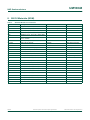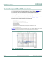
1
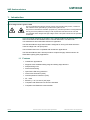
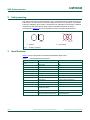
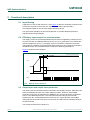
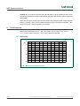
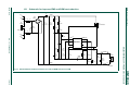
UM10848 SSL5231DB1242 230 V/4 W non-isolated buck-boost candle-form dimmable LED driver dual demo board Rev. 1.2 — 25 March 2015 User manual Document information Info Content Keywords SSL5231DB1242, SSL5231T, non-isolated buck-boost topology, LED driver controller, external MOSFET switch, dimmable candle-form applications, SO8 package Abstract This user manual describes the performance, technical data, and the connection of the SSL5231DB1242 dual demo board. The demo board uses non-isolated buck-boost topology. This SSL5231DB1242 dual demo board is designed for dimmable candle-form applications. It operates at 230 V (AC) with an output voltage of approximately 90 V. UM10848 NXP Semiconductors SSL5231DB1242 230 V/4 W LED driver demo board Revision history Rev Date Description v.1.2 20150325 updated issue v.1.1 20150119 updated issue v.1 20141024 first issue Contact information For more information, please visit: http://www.nxp.com For sales office addresses, please send an email to: [email protected] UM10848 User manual All information provided in this document is subject to legal disclaimers. Rev. 1.2 — 25 March 2015 © NXP Semiconductors N.V. 2015. All rights reserved. 2 of 18 UM10848 NXP Semiconductors SSL5231DB1242 230 V/4 W LED driver demo board 1. Introduction WARNING Lethal voltage and fire ignition hazard The non-insulated high voltages that are present when operating this product, constitute a risk of electric shock, personal injury, death and/or ignition of fire. This product is intended for evaluation purposes only. It shall be operated in a designated test area by personnel qualified according to local requirements and labor laws to work with non-insulated mains voltages and high-voltage circuits. This product shall never be operated unattended. This user manual describes the operation of the SSL5231DB1242 dual demo board. The demo board features the MOSFET driver controller SSL5231T in a 230 V/4 W non-isolated buck-boost dimmable LED driver application. The SSL5231DB1242 single demo board is designed for driving LED loads with 90 V nominal voltage and 4 W input power. The PCB dimensions are compatible with candle-form applications. The SSL5231DB1242 demo board provides a simple and highly efficient solution for Solid-State Lighting (SSL) applications. 1.1 Features • • • • • • • • • • • UM10848 User manual Candle-form applications Supports most available leading-edge and trailing-edge dimmers Deep dimming level Flicker-free dimming Open/short LED string protection OverCurrent Protection (OCP) OverTemperature Protection (OTP) PF > 0.86 Efficiency > 75 % at 230 V (AC) input Compliant with IEC61000-3-2 harmonic standard Compliant with EN55015 conducted EMI All information provided in this document is subject to legal disclaimers. Rev. 1.2 — 25 March 2015 © NXP Semiconductors N.V. 2015. All rights reserved. 3 of 18 UM10848 NXP Semiconductors SSL5231DB1242 230 V/4 W LED driver demo board 2. Safety warning The demo board input is connected to the 230 V (AC) mains supply. Avoid touching the board while it is connected to the mains voltage and when it is in operation. An isolated housing is obligatory when used in uncontrolled, non-laboratory environments. Galvanic isolation from the mains phase using a fixed or variable transformer is always recommended. Figure 1 shows the symbols on how to recognize these devices. 019aab174 019aab173 a. Isolated Fig 1. b. Not isolated Isolation symbols 3. Specifications Table 1 lists the specification of the SSL5231DB1242 demo board. Table 1. UM10848 User manual SSL5231DB1242 specifications Symbol Parameter Value Vmains AC mains supply voltage 230 V (AC); 10 % Pin input power 4W VLED output voltage 90 V ILED output current 37 mA ILED(ripple) output current ripple 25 % (100 Hz) ILED/Vmains line regulation 3 % at Vmains = 207 V to 253 V ILED/VLED load regulation 5 % at VLED; 15 % to +7.7 % efficiency 75 %; at 230 V (AC)/50 Hz PF power factor > 0.86 at 230 V (AC)/50 Hz Toper operating temperature 40 C to +105 C - board dimensions 60 mm 40 mm - conducted electromagnetic Interference (EMI) EN55015 - IEC61000-3-2 class D (for Pin < 25 W limit) - dimmer compatibility (stable light output above on/off point) 80 % dimmer compatibility for 2 lamps/dimmer All information provided in this document is subject to legal disclaimers. Rev. 1.2 — 25 March 2015 © NXP Semiconductors N.V. 2015. All rights reserved. 4 of 18 UM10848 NXP Semiconductors SSL5231DB1242 230 V/4 W LED driver demo board 4. Board photographs Figure 2 shows the top view and bottom view of the SSL5231DB1242 demo board. The board has been designed as a dual board. For dimmer tests, it is assumed that at least two lamps of 4 W are connected to one dimmer. However, the board can also be tested separately by removing the blue jumpers which can be seen in Figure 2 (a). At the left connector of the board (Figure 2 (a)), the AC mains (230 V) must be added. At the right connector, the LED load (90 V) must be connected. The inner part of the board can be taken out. It has a diameter of 28 mm which fits in a candle lamp. a. Top view Fig 2. b. Bottom view SSL5231DB1242 dual demo board photographs UM10848 User manual All information provided in this document is subject to legal disclaimers. Rev. 1.2 — 25 March 2015 © NXP Semiconductors N.V. 2015. All rights reserved. 5 of 18 UM10848 NXP Semiconductors SSL5231DB1242 230 V/4 W LED driver demo board 5. Functional description 5.1 Input filtering Capacitors C1 and C2 and inductor L1 (see Figure 10) filter the switching current from the buck-boost converter to the mains AC. Capacitors C1 and C2 also provide a low-impedance path for the converter output switching current. The input series resistance of 660 and capacitor C1 provide adequate protection against transient surge voltages. 5.2 Efficiency improvement for universal mains The supply current for the SSL5231DB1242 demo board is supplied by resistors R3 and R4. The IC draws an additional start-up current (ICC(startup)) just before VCC reaches the start-up voltage level (Vstartup). The supply current in operation is therefore lower than during start-up conditions, preventing lamp flicker when the mains voltage is increased or decreased slowly. This mechanism also increases the dimming performance. Figure 3 shows the basic behavior. 9VWDUWXS 99&& 9&& O&&VWDUWXS O&&RSHU ,&& 9*$7( DDD Fig 3. Start-up current waveform 5.3 Output open and output short protection The driver board is protected when the LED load is accidentally left open. When the LED load is accidentally left open, the output voltage increases. When the OverVoltage Protection (OVP) level is reached on the DEMOVP pin, the OVP protection is triggered. OVP is a non-latched protection. It recovers when the LED string is reconnected. Resistors R6, R7, and R8 determine the OVP level. An output capacitor C56 voltage rating higher than the DC level which occurs when the LED load is accidentally left open must be ensured. The measured OVP level is about 99 V. UM10848 User manual All information provided in this document is subject to legal disclaimers. Rev. 1.2 — 25 March 2015 © NXP Semiconductors N.V. 2015. All rights reserved. 6 of 18 UM10848 NXP Semiconductors SSL5231DB1242 230 V/4 W LED driver demo board Remark: Do not reconnect the LED string directly after an OVP condition because it can permanently damage the LEDs. Switch off the mains and wait until the output capacitor is discharged. When the LED driver output of the board is shorted, the maximum ISNS voltage limits the primary converter current. The converter frequency drops to its absolute minimum. This mode is very safe. The input power is very limited. 6. Performance During performance tests Vmains = 230 V (AC) with a 20 % margin, Tamb = 25 C, ILED = 37.4 mA typical, and VLED = 90 V unless otherwise specified. 6.1 Efficiency DDD Ș Fig 4. UM10848 User manual 9PDLQV9 Efficiency as a function of Vmains All information provided in this document is subject to legal disclaimers. Rev. 1.2 — 25 March 2015 © NXP Semiconductors N.V. 2015. All rights reserved. 7 of 18 UM10848 NXP Semiconductors SSL5231DB1242 230 V/4 W LED driver demo board 6.2 Power factor DDD 3) Fig 5. 9PDLQV9 Power factor as a function of Vmains 6.3 Line regulation DDD ,/(' P$ Fig 6. UM10848 User manual 9PDLQV9 Line regulation All information provided in this document is subject to legal disclaimers. Rev. 1.2 — 25 March 2015 © NXP Semiconductors N.V. 2015. All rights reserved. 8 of 18 UM10848 NXP Semiconductors SSL5231DB1242 230 V/4 W LED driver demo board 6.4 Load regulation DDD ,/(' P$ Fig 7. 9/('9 Load regulation 6.5 Output ripple DDD ,/('ULSSOH Fig 8. UM10848 User manual 9PDLQV9 Output ripple as a function of Vmains All information provided in this document is subject to legal disclaimers. Rev. 1.2 — 25 March 2015 © NXP Semiconductors N.V. 2015. All rights reserved. 9 of 18 UM10848 NXP Semiconductors SSL5231DB1242 230 V/4 W LED driver demo board 6.6 ElectroMagnetic Interference (EMI) Figure 9 shows the conducted EMI result of the SSL5231DB1242 demo board. Fig 9. UM10848 User manual Conducted EMI All information provided in this document is subject to legal disclaimers. Rev. 1.2 — 25 March 2015 © NXP Semiconductors N.V. 2015. All rights reserved. 10 of 18 xxxxxxxxxxxxxxxxxxxxx xxxxxxxxxxxxxxxxxxxxxxxxxx xxxxxxx x x x xxxxxxxxxxxxxxxxxxxxxxxxxxxxxx xxxxxxxxxxxxxxxxxxx xx xx xxxxx xxxxxxxxxxxxxxxxxxxxxxxxxxx xxxxxxxxxxxxxxxxxxx xxxxxx xxxxxxxxxxxxxxxxxxxxxxxxxxxxxxxxxxx xxxxxxxxxxxx x x xxxxxxxxxxxxxxxxxxxxx xxxxxxxxxxxxxxxxxxxxxxxxxxxxxx xxxxx xxxxxxxxxxxxxxxxxxxxxxxxxxxxxxxxxxxxxxxxxxxxxxxxxx xxxxxxxx xxxxxxxxxxxxxxxxxxxxxxxxx xxxxxxxxxxxxxxxxxxxx xxx NXP Semiconductors UM10848 User manual 7. Schematic / ( / %' 0'6 ( / ; ( ) ( / $ / 5 Nȍ a a 9%86 P+ & Q) 9 59 9 1 ȍ : ( 5 1 ȍ : 5 ȍ 5 0ȍ ' %$6 9&& 5 Nȍ ( / 8 ',0 &203 9&& ,616 5 Nȍ & Q) 9 & ) 9 & ) 9 66/7 '(0293 *1' QF 6: ' (6- FORVH WRSLQ 5 ȍ & S) 9 0 5 Nȍ 5 Nȍ 5 Nȍ *1' ( :,5( ( 5 Nȍ / P+ ; & ) 9 ( :,5( ( 9/(' 9 3 DDD UM10848 11 of 18 © NXP Semiconductors N.V. 2015. All rights reserved. 3 Fig 10. SSL5231DB1242 demo board schematic diagram 0 SSL5231DB1242 230 V/4 W LED driver demo board Rev. 1.2 — 25 March 2015 All information provided in this document is subject to legal disclaimers. ( / 5 4 6381& 5 Nȍ 9$& ( ' %$6 5 0ȍ & Q) 9 UM10848 NXP Semiconductors SSL5231DB1242 230 V/4 W LED driver demo board 8. Bill Of Materials (BOM) Table 2. Reference SSL5231DB1242 bill of materials Description and values Part number Manufacturer BD1 bridge rectifier; 1000 V; 500 mA MD5S Rectron C1; C2 capacitor; 47 nF; 5 %; 400 V; PET; THT CL21-400V-0.047µF/K AIDI C4 capacitor; 2.2 F; 10 %; 50 V; X7R; 0805 C2012X7R1H225K125AC TDK C20 capacitor; 2.2 F; 10 %; 6.3 V; X7R; 0603 C1608X7R0J225K080AB TDK C55 capacitor; 47 nF; 10 %; 50 V; X7R; 0603 - - C56 capacitor; 68 F; 20 %; 100 V; ALU; 8 mm 20 mm 100ZLJ68M8X20 Rubycon C57 capacitor; 22 pF; 10 %; 50 V; X7R; 0603 - - D1; D20 diode; 100 V; 250 mA BAS316 NXP Semiconductors D2 diode; 600 V; 1 A ES1J Fairchild F1 fuse; slow blow; 250 V (AC); 1 A MCPMP 1A 250V Multicomp L1 inductor; 3.3 mH; 100 mA 22R335C Murata L2 inductor; 4.7 mH; 10 %; 0.11 A 744731472 Würth Elektronik Q1 MOSFET-N; 650 V; 1.8 A SPU02N60C3 Infineon R1; R2 resistor; 330 ; 5 %; 2 W; MFP2 MFP2-330RJI Welwyn Components R3; R4 resistor; 180 k; 1 %; 250 mW; 1206 - - R5 resistor; 8.2 ; 1 %; 63 mW; 0603 - - R6 resistor; 5.6 k; 1 %; 63 mW; 0603 - - R7 resistor; 150 k; 1 %; 250 mW; 1206 - - R8 resistor; 160 k; 1 %; 250 mW; 1206 - - R20; R21 resistor; 1.3 M; 1 %; 250 mW; 1206 - - R22 resistor; 27 k; 1 %; 63 mW; 0603 - - R23 resistor; 910 k; 1 %; 63 mW; 0603 - - R24 resistor; 220 ; 1 %; 63 mW; 0603 - - R25 resistor; 150 k; 1 %; 63 mW; 0603 - - RV1 resistor; VDR; 275 V; 36 J VDRS07H275BSE Vishay U1 IC; buck-boost LED driver SSL5231T SSL5231T NXP Semiconductors UM10848 User manual All information provided in this document is subject to legal disclaimers. Rev. 1.2 — 25 March 2015 © NXP Semiconductors N.V. 2015. All rights reserved. 12 of 18 UM10848 NXP Semiconductors SSL5231DB1242 230 V/4 W LED driver demo board 9. Board layout a. Top view b. Bottom view Fig 11. SSL5231DB1242 demo board layout a. Top view b. Bottom view Fig 12. SSL5231DB1242 demo board component placement UM10848 User manual All information provided in this document is subject to legal disclaimers. Rev. 1.2 — 25 March 2015 © NXP Semiconductors N.V. 2015. All rights reserved. 13 of 18 UM10848 NXP Semiconductors SSL5231DB1242 230 V/4 W LED driver demo board 10. Errata for improved EMI and BOM cost reduction All measured data given in this user manual is based on the schematic (Figure 10) and the current mounted demo board SSL5231DB1242. It shows that EMC compliance, for the current setup, can only be achieved by the complete shielding of the board. Further investigation shows that, even with a reduced BOM (Bill of Material), major behavior improvements for EMC compliance (without shielding) can be achieved. To reduce cost, the design and the board can be modified (see Figure 14). Table 3 shows the BOM of the modified schematic and improved EMI. Modifications for the modified schematic and improved EMI: • • • • • • • Remove fuse F1 Move resistor R1 to the footprint of F1 Short the footprint of resistor R1 using a wire Remove diode D1 Remove diode D20 Replace the current resistor R24 (220 ) by a 0 resistor or a wire Remove capacitor C57 Figure 13 shows the improved conducted EMI result of the SSL5231DB1242 demo board with the modifications indicated above. No other side effects have been found. Fig 13. Improved conducted EMI UM10848 User manual All information provided in this document is subject to legal disclaimers. Rev. 1.2 — 25 March 2015 © NXP Semiconductors N.V. 2015. All rights reserved. 14 of 18 xxxxxxxxxxxxxxxxxxxxx xxxxxxxxxxxxxxxxxxxxxxxxxx xxxxxxx x x x xxxxxxxxxxxxxxxxxxxxxxxxxxxxxx xxxxxxxxxxxxxxxxxxx xx xx xxxxx xxxxxxxxxxxxxxxxxxxxxxxxxxx xxxxxxxxxxxxxxxxxxx xxxxxx xxxxxxxxxxxxxxxxxxxxxxxxxxxxxxxxxxx xxxxxxxxxxxx x x xxxxxxxxxxxxxxxxxxxxx xxxxxxxxxxxxxxxxxxxxxxxxxxxxxx xxxxx xxxxxxxxxxxxxxxxxxxxxxxxxxxxxxxxxxxxxxxxxxxxxxxxxx xxxxxxxx xxxxxxxxxxxxxxxxxxxxxxxxx xxxxxxxxxxxxxxxxxxxx xxx NXP Semiconductors UM10848 User manual 10.1 Schematic for improved EMI and BOM cost reduction / ( / %' 0'6 ( / ( ; 5 / ȍ : ( / 5 Nȍ a a 9%86 P+ & Q) 9 5 0ȍ & Q) 9 5 Nȍ 59 9 5 0ȍ 9$& ( ( 1 5 Nȍ ( 1 8 ',0 &203 9&& ,616 5 Nȍ & Q) 9 & ) 9 & ) 9 66/7 '(0293 *1' QF 6: ' (65 ȍ FORVH WRSLQ 5 Nȍ 0 5 Nȍ 5 Nȍ *1' ( :,5( ( 5 Nȍ / P+ ; & ) 9 ( :,5( ( 9/(' 9 3 DDD UM10848 15 of 18 © NXP Semiconductors N.V. 2015. All rights reserved. 3 Fig 14. SSL5231DB1242 modified schematic for reduced BOM and improved EMI 0 SSL5231DB1242 230 V/4 W LED driver demo board Rev. 1.2 — 25 March 2015 All information provided in this document is subject to legal disclaimers. ( 1 5 1 ȍ : 4 6381& UM10848 NXP Semiconductors SSL5231DB1242 230 V/4 W LED driver demo board 11. BOM for improved EMI and BOM cost reduction Table 3. SSL5231DB1242 modified demo board bill of materials Reference Description and values Part number Manufacturer BD1 bridge rectifier; 1000 V; 500 mA MD5S Rectron C1; C2 capacitor; 47 nF; 5 %; 400 V; PET; THT CL21-400V-0.047µF/K AIDI C4 capacitor; 2.2 F; 10 %; 50 V; X7R; 0805 C2012X7R1H225K125AC TDK C20 capacitor; 2.2 F; 10 %; 6.3 V; X7R; 0603 C1608X7R0J225K080AB TDK C55 capacitor; 47 nF; 10 %; 50 V; X7R; 0603 - - C56 capacitor; 68 F; 20 %; 100 V; ALU; 8 mm 20 mm 100ZLJ68M8X20 Rubycon D2 diode; 600 V; 1 A ES1J Fairchild L1 inductor; 3.3 mH; 100 mA 22R335C Murata L2 inductor; 4.7 mH; 10 %; 0.11 A 744731472 Würth Elektronik Q1 MOSFET-N; 650 V; 1.8 A SPU02N60C3 Infineon R1; R2 resistor; 330 ; 5 %; 2 W; MFP2 MFP2-330RJI Welwyn Components R3; R4 resistor; 180 k; 1 %; 250 mW; 1206 - - R5 resistor; 8.2 ; 1 %; 63 mW; 0603 - - R6 resistor; 5.6 k; 1 %; 63 mW; 0603 - - R7 resistor; 150 k; 1 %; 250 mW; 1206 - - R8 resistor; 160 k; 1 %; 250 mW; 1206 - - R20; R21 resistor; 1.3 M; 1 %; 250 mW; 1206 - - R22 resistor; 27 k; 1 %; 63 mW; 0603 - - R23 resistor; 910 k; 1 %; 63 mW; 0603 - - R25 resistor; 150 k; 1 %; 63 mW; 0603 - - RV1 resistor; VDR; 275 V; 36 J VDRS07H275BSE Vishay U1 IC; buck-boost LED driver SSL5231T SSL5231T NXP Semiconductors 12. Abbreviations Table 4. Abbreviations Acronym Description EMI ElectroMagnetic Interference LED Light-Emitting Diode OCP OverCurrent Protection OTP OverTemperature Protection PF Power Factor SSL Solid-State Lighting 13. References [1] UM10848 User manual SSL5231T data sheet — Compact high power factor dimmable LED driver IC All information provided in this document is subject to legal disclaimers. Rev. 1.2 — 25 March 2015 © NXP Semiconductors N.V. 2015. All rights reserved. 16 of 18 UM10848 NXP Semiconductors SSL5231DB1242 230 V/4 W LED driver demo board 14. Legal information 14.1 Definitions Draft — The document is a draft version only. The content is still under internal review and subject to formal approval, which may result in modifications or additions. NXP Semiconductors does not give any representations or warranties as to the accuracy or completeness of information included herein and shall have no liability for the consequences of use of such information. NXP Semiconductors does not accept any liability related to any default, damage, costs or problem which is based on any weakness or default in the customer’s applications or products, or the application or use by customer’s third party customer(s). Customer is responsible for doing all necessary testing for the customer’s applications and products using NXP Semiconductors products in order to avoid a default of the applications and the products or of the application or use by customer’s third party customer(s). NXP does not accept any liability in this respect. Export control — This document as well as the item(s) described herein may be subject to export control regulations. Export might require a prior authorization from competent authorities. 14.2 Disclaimers Limited warranty and liability — Information in this document is believed to be accurate and reliable. However, NXP Semiconductors does not give any representations or warranties, expressed or implied, as to the accuracy or completeness of such information and shall have no liability for the consequences of use of such information. NXP Semiconductors takes no responsibility for the content in this document if provided by an information source outside of NXP Semiconductors. In no event shall NXP Semiconductors be liable for any indirect, incidental, punitive, special or consequential damages (including - without limitation - lost profits, lost savings, business interruption, costs related to the removal or replacement of any products or rework charges) whether or not such damages are based on tort (including negligence), warranty, breach of contract or any other legal theory. Notwithstanding any damages that customer might incur for any reason whatsoever, NXP Semiconductors’ aggregate and cumulative liability towards customer for the products described herein shall be limited in accordance with the Terms and conditions of commercial sale of NXP Semiconductors. Right to make changes — NXP Semiconductors reserves the right to make changes to information published in this document, including without limitation specifications and product descriptions, at any time and without notice. This document supersedes and replaces all information supplied prior to the publication hereof. Suitability for use — NXP Semiconductors products are not designed, authorized or warranted to be suitable for use in life support, life-critical or safety-critical systems or equipment, nor in applications where failure or malfunction of an NXP Semiconductors product can reasonably be expected to result in personal injury, death or severe property or environmental damage. NXP Semiconductors and its suppliers accept no liability for inclusion and/or use of NXP Semiconductors products in such equipment or applications and therefore such inclusion and/or use is at the customer’s own risk. Applications — Applications that are described herein for any of these products are for illustrative purposes only. NXP Semiconductors makes no representation or warranty that such applications will be suitable for the specified use without further testing or modification. Customers are responsible for the design and operation of their applications and products using NXP Semiconductors products, and NXP Semiconductors accepts no liability for any assistance with applications or customer product design. It is customer’s sole responsibility to determine whether the NXP Semiconductors product is suitable and fit for the customer’s applications and products planned, as well as for the planned application and use of customer’s third party customer(s). Customers should provide appropriate design and operating safeguards to minimize the risks associated with their applications and products. Evaluation products — This product is provided on an “as is” and “with all faults” basis for evaluation purposes only. NXP Semiconductors, its affiliates and their suppliers expressly disclaim all warranties, whether express, implied or statutory, including but not limited to the implied warranties of non-infringement, merchantability and fitness for a particular purpose. The entire risk as to the quality, or arising out of the use or performance, of this product remains with customer. In no event shall NXP Semiconductors, its affiliates or their suppliers be liable to customer for any special, indirect, consequential, punitive or incidental damages (including without limitation damages for loss of business, business interruption, loss of use, loss of data or information, and the like) arising out the use of or inability to use the product, whether or not based on tort (including negligence), strict liability, breach of contract, breach of warranty or any other theory, even if advised of the possibility of such damages. Notwithstanding any damages that customer might incur for any reason whatsoever (including without limitation, all damages referenced above and all direct or general damages), the entire liability of NXP Semiconductors, its affiliates and their suppliers and customer’s exclusive remedy for all of the foregoing shall be limited to actual damages incurred by customer based on reasonable reliance up to the greater of the amount actually paid by customer for the product or five dollars (US$5.00). The foregoing limitations, exclusions and disclaimers shall apply to the maximum extent permitted by applicable law, even if any remedy fails of its essential purpose. Safety of high-voltage evaluation products — The non-insulated high voltages that are present when operating this product, constitute a risk of electric shock, personal injury, death and/or ignition of fire. This product is intended for evaluation purposes only. It shall be operated in a designated test area by personnel that is qualified according to local requirements and labor laws to work with non-insulated mains voltages and high-voltage circuits. The product does not comply with IEC 60950 based national or regional safety standards. NXP Semiconductors does not accept any liability for damages incurred due to inappropriate use of this product or related to non-insulated high voltages. Any use of this product is at customer’s own risk and liability. The customer shall fully indemnify and hold harmless NXP Semiconductors from any liability, damages and claims resulting from the use of the product. Translations — A non-English (translated) version of a document is for reference only. The English version shall prevail in case of any discrepancy between the translated and English versions. 14.3 Trademarks Notice: All referenced brands, product names, service names and trademarks are the property of their respective owners. GreenChip — is a trademark of NXP Semiconductors N.V. UM10848 User manual All information provided in this document is subject to legal disclaimers. Rev. 1.2 — 25 March 2015 © NXP Semiconductors N.V. 2015. All rights reserved. 17 of 18 UM10848 NXP Semiconductors SSL5231DB1242 230 V/4 W LED driver demo board 15. Contents 1 1.1 2 3 4 5 5.1 5.2 5.3 6 6.1 6.2 6.3 6.4 6.5 6.6 7 8 9 10 10.1 11 12 13 14 14.1 14.2 14.3 15 Introduction . . . . . . . . . . . . . . . . . . . . . . . . . . . . 3 Features . . . . . . . . . . . . . . . . . . . . . . . . . . . . . . 3 Safety warning . . . . . . . . . . . . . . . . . . . . . . . . . . 4 Specifications. . . . . . . . . . . . . . . . . . . . . . . . . . . 4 Board photographs . . . . . . . . . . . . . . . . . . . . . . 5 Functional description . . . . . . . . . . . . . . . . . . . 6 Input filtering . . . . . . . . . . . . . . . . . . . . . . . . . . . 6 Efficiency improvement for universal mains . . . 6 Output open and output short protection . . . . . 6 Performance . . . . . . . . . . . . . . . . . . . . . . . . . . . . 7 Efficiency . . . . . . . . . . . . . . . . . . . . . . . . . . . . . 7 Power factor . . . . . . . . . . . . . . . . . . . . . . . . . . . 8 Line regulation . . . . . . . . . . . . . . . . . . . . . . . . . 8 Load regulation . . . . . . . . . . . . . . . . . . . . . . . . . 9 Output ripple . . . . . . . . . . . . . . . . . . . . . . . . . . . 9 ElectroMagnetic Interference (EMI) . . . . . . . . 10 Schematic . . . . . . . . . . . . . . . . . . . . . . . . . . . . . 11 Bill Of Materials (BOM) . . . . . . . . . . . . . . . . . . 12 Board layout . . . . . . . . . . . . . . . . . . . . . . . . . . . 13 Errata for improved EMI and BOM cost reduction . . . . . . . . . . . . . . . . . . . . . . . . . . . . . 14 Schematic for improved EMI and BOM cost reduction . . . . . . . . . . . . . . . . . . . . . . . . . . . . . 15 BOM for improved EMI and BOM cost reduction . . . . . . . . . . . . . . . . . . . . . . . . . . . . . 16 Abbreviations . . . . . . . . . . . . . . . . . . . . . . . . . . 16 References . . . . . . . . . . . . . . . . . . . . . . . . . . . . 16 Legal information. . . . . . . . . . . . . . . . . . . . . . . 17 Definitions . . . . . . . . . . . . . . . . . . . . . . . . . . . . 17 Disclaimers . . . . . . . . . . . . . . . . . . . . . . . . . . . 17 Trademarks. . . . . . . . . . . . . . . . . . . . . . . . . . . 17 Contents . . . . . . . . . . . . . . . . . . . . . . . . . . . . . . 18 Please be aware that important notices concerning this document and the product(s) described herein, have been included in section ‘Legal information’. © NXP Semiconductors N.V. 2015. All rights reserved. For more information, please visit: http://www.nxp.com For sales office addresses, please send an email to: [email protected] Date of release: 25 March 2015 Document identifier: UM10848