1
PIC32MX3XX/4XX Family
Data Sheet
64/100-Pin General Purpose and USB
32-Bit Flash Microcontrollers
© 2008 Microchip Technology Inc.
Preliminary
DS61143D
Note the following details of the code protection feature on Microchip devices:
•
Microchip products meet the specification contained in their particular Microchip Data Sheet.
•
Microchip believes that its family of products is one of the most secure families of its kind on the market today, when used in the
intended manner and under normal conditions.
•
There are dishonest and possibly illegal methods used to breach the code protection feature. All of these methods, to our
knowledge, require using the Microchip products in a manner outside the operating specifications contained in Microchip’s Data
Sheets. Most likely, the person doing so is engaged in theft of intellectual property.
•
Microchip is willing to work with the customer who is concerned about the integrity of their code.
•
Neither Microchip nor any other semiconductor manufacturer can guarantee the security of their code. Code protection does not
mean that we are guaranteeing the product as “unbreakable.”
Code protection is constantly evolving. We at Microchip are committed to continuously improving the code protection features of our
products. Attempts to break Microchip’s code protection feature may be a violation of the Digital Millennium Copyright Act. If such acts
allow unauthorized access to your software or other copyrighted work, you may have a right to sue for relief under that Act.
Information contained in this publication regarding device
applications and the like is provided only for your convenience
and may be superseded by updates. It is your responsibility to
ensure that your application meets with your specifications.
MICROCHIP MAKES NO REPRESENTATIONS OR
WARRANTIES OF ANY KIND WHETHER EXPRESS OR
IMPLIED, WRITTEN OR ORAL, STATUTORY OR
OTHERWISE, RELATED TO THE INFORMATION,
INCLUDING BUT NOT LIMITED TO ITS CONDITION,
QUALITY, PERFORMANCE, MERCHANTABILITY OR
FITNESS FOR PURPOSE. Microchip disclaims all liability
arising from this information and its use. Use of Microchip
devices in life support and/or safety applications is entirely at
the buyer’s risk, and the buyer agrees to defend, indemnify and
hold harmless Microchip from any and all damages, claims,
suits, or expenses resulting from such use. No licenses are
conveyed, implicitly or otherwise, under any Microchip
intellectual property rights.
Trademarks
The Microchip name and logo, the Microchip logo, Accuron,
dsPIC, KEELOQ, KEELOQ logo, MPLAB, PIC, PICmicro,
PICSTART, PRO MATE, rfPIC and SmartShunt are registered
trademarks of Microchip Technology Incorporated in the
U.S.A. and other countries.
FilterLab, Linear Active Thermistor, MXDEV, MXLAB,
SEEVAL, SmartSensor and The Embedded Control Solutions
Company are registered trademarks of Microchip Technology
Incorporated in the U.S.A.
Analog-for-the-Digital Age, Application Maestro, CodeGuard,
dsPICDEM, dsPICDEM.net, dsPICworks, dsSPEAK, ECAN,
ECONOMONITOR, FanSense, In-Circuit Serial
Programming, ICSP, ICEPIC, Mindi, MiWi, MPASM, MPLAB
Certified logo, MPLIB, MPLINK, mTouch, PICkit, PICDEM,
PICDEM.net, PICtail, PIC32 logo, PowerCal, PowerInfo,
PowerMate, PowerTool, REAL ICE, rfLAB, Select Mode, Total
Endurance, UNI/O, WiperLock and ZENA are trademarks of
Microchip Technology Incorporated in the U.S.A. and other
countries.
SQTP is a service mark of Microchip Technology Incorporated
in the U.S.A.
All other trademarks mentioned herein are property of their
respective companies.
© 2008, Microchip Technology Incorporated, Printed in the
U.S.A., All Rights Reserved.
Printed on recycled paper.
Microchip received ISO/TS-16949:2002 certification for its worldwide
headquarters, design and wafer fabrication facilities in Chandler and
Tempe, Arizona; Gresham, Oregon and design centers in California
and India. The Company’s quality system processes and procedures
are for its PIC® MCUs and dsPIC® DSCs, KEELOQ® code hopping
devices, Serial EEPROMs, microperipherals, nonvolatile memory and
analog products. In addition, Microchip’s quality system for the design
and manufacture of development systems is ISO 9001:2000 certified.
DS61143D-page ii
Preliminary
© 2008 Microchip Technology Inc.
PIC32MX3XX/4XX
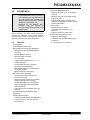
High-Performance 80 MHz MIPS-Based 32-bit Flash Microcontroller
64/100-Pin General Purpose and USB
High-Performance 32-bit RISC CPU:
• MIPS32® M4K™ 32-bit Core with 5-Stage Pipeline
• 80 MHz Maximum Frequency
• 1.56 DMIPS/MHz (Dhrystone 2.1) Performance
at 0 Wait State Flash Access
• Single-Cycle Multiply and High-Performance
Divide Unit
• MIPS16e™ Mode for Up to 40% Smaller Code
Size
• User and Kernel Modes to Enable Robust
Embedded System
• Two Sets of 32 Core Register Files (32-bit) to
Reduce Interrupt Latency
• Prefetch Cache Module to Speed Execution from
Flash
Microcontroller Features:
• Operating Voltage Range of 2.3V to 3.6V
• 32K to 512K Flash Memory (plus an additional
12KB of Boot Flash)
• 8K to 32K SRAM Memory
• Pin-Compatible with Most PIC24/dsPIC® Devices
• Multiple Power Management Modes
• Multiple Interrupt Vectors with Individually
Programmable Priority
• Fail-Safe Clock Monitor Mode
• Configurable Watchdog Timer with On-Chip
Low-Power RC Oscillator for Reliable Operation
Peripheral Features:
• Atomic SET, CLEAR and INVERT Operation on
Select Peripheral Registers
• Up to 4-Channel Hardware DMA Controller with
Automatic Data Size Detection
• USB 2.0 Compliant Full Speed Device and
On-The-Go (OTG) Controller
• USB has a Dedicated DMA Channel
• 10 MHz to 40 MHz Crystal Oscillator
• Internal 8 MHz and 32 kHz Oscillators
© 2008 Microchip Technology Inc.
• Separate PLLs for CPU and USB Clocks
• Two I2C™ Modules
• Two UART Modules with:
- RS-232, RS-485 and LIN 1.2 support
- IrDA® with On-Chip Hardware Encoder and
Decoder
• Parallel Master and Slave Port (PMP/PSP) with
8-bit and 16-bit Data and Up to 16 Address Lines
• Hardware Real-Time Clock/Calendar (RTCC)
• Five 16-bit Timers/Counters (two 16-bit pairs combine to create two 32-bit timers)
• Five Capture Inputs
• Five Compare/PWM Outputs
• Five External Interrupt Pins
• High-Speed I/O Pins Capable of Toggling at Up to
80 MHz
• High-Current Sink/Source (18 mA/18 mA) on
All I/O Pins
• Configurable Open-Drain Output on Digital I/O
Pins
Debug Features:
• Two Programming and Debugging Interfaces:
- 2-Wire Interface with Unintrusive Access and
Real-time Data Exchange with Application
- 4-wire MIPS Standard Enhanced JTAG
interface
• Unintrusive Hardware-Based Instruction Trace
• IEEE Std 1149.2 Compatible (JTAG) Boundary
Scan
Analog Features:
• Up to 16-Channel 10-bit Analog-to-Digital
Converter:
- 500 ksps Conversion Rate
- Conversion Available During Sleep, Idle
• Two Analog Comparators
• 5.5V Tolerant Input Pins (digital pins only)
Preliminary
DS61143D-page 1
PIC32MX3XX/4XX
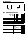
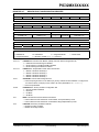
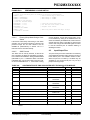
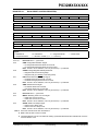
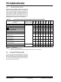
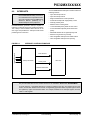
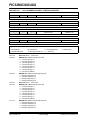
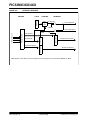
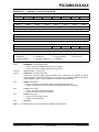
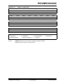
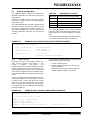
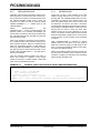
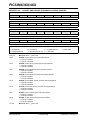
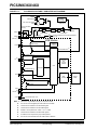
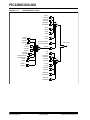
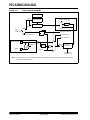
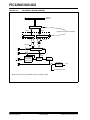
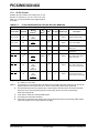
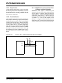
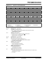
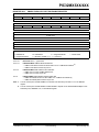
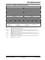
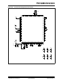
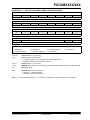
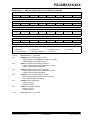
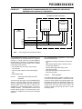
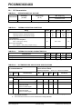
FIGURE 1:
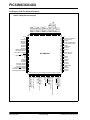
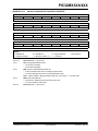
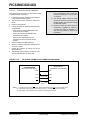
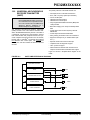
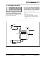
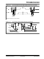
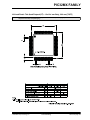
PIC32MX3XX/4XX PACKAGE OUTLINE DRAWING
TQFP 64-Pin
10 x 10 mm
TQFP 100-Pin
12 x 12 mm
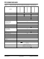
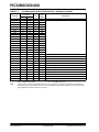
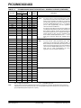
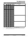
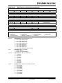
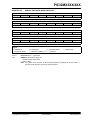
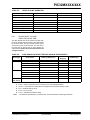
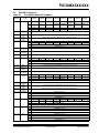
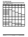
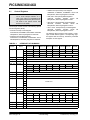
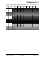
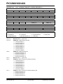
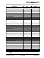
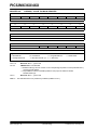
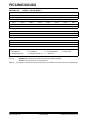
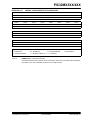
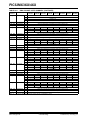
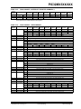
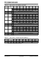
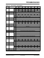
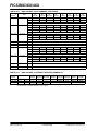
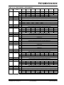
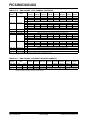
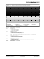
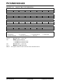
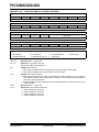
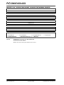
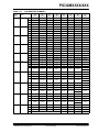
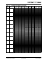
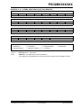
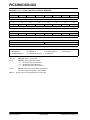
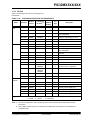
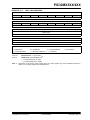
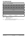
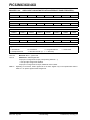
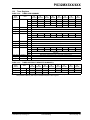
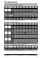
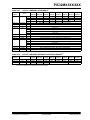
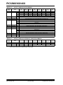
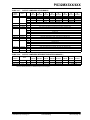
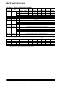
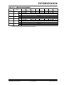
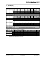
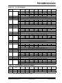
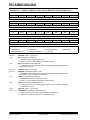
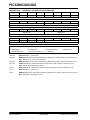
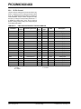
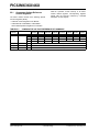
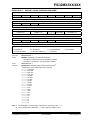
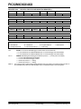
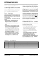
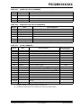
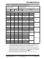
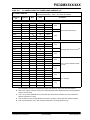
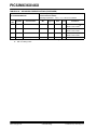
TABLE 2:
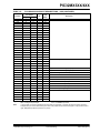
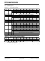
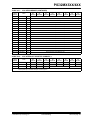
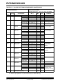
PIC32MX3XX/4XX GENERAL PURPOSE – FEATURES
10-bit
A/D (ch)
Comparators
No
2/2/2
16
2
Yes Yes
No
2/2/2
16
2
Yes Yes
No
2/2/2
16
2
Yes Yes
No
2/2/2
16
2
Yes Yes
Yes
No
2/2/2
16
2
Yes Yes
Yes
No
2/2/2
16
2
Yes Yes
0
Yes
No
2/2/2
16
2
Yes Yes
4
Yes
No
2/2/2
16
2
Yes Yes
5/5/5
4
Yes Yes
2/2/2
16
2
Yes Yes
5/5/5
4
Yes Yes
2/2/2
16
2
Yes Yes
MHz
PIC32MX320F032H
64
40
32/8
5/5/5
0
Yes
PIC32MX320F064H
64
80
64/16
5/5/5
0
Yes
PIC32MX320F128H
64
80
128/16
5/5/5
0
Yes
PIC32MX340F128H
64
80
128/32
5/5/5
0
Yes
PIC32MX340F256H
64
80
256/32
5/5/5
4
PIC32MX340F512H
64
80
512/32
5/5/5
4
PIC32MX320F128L
100
80
128/16
5/5/5
PIC32MX340F128L
100
80
128/32
5/5/5
PIC32MX360F256L
100
80
256/32
PIC32MX360F512L
100
80
512/32
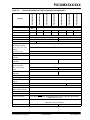
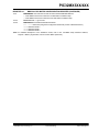
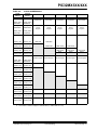
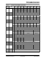
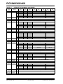
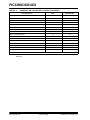
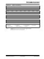
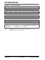
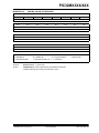
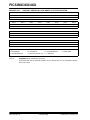
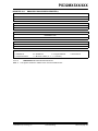
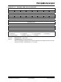
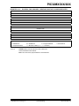
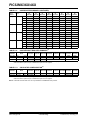
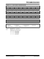
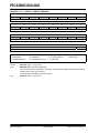
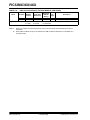
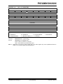
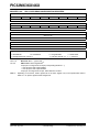
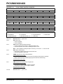
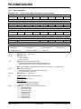
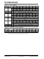
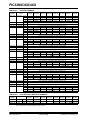
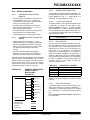
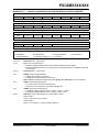
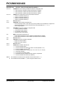
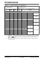
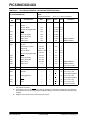
TABLE 3:
JTAG
EUART/
SPI/
I2C™
Timers/
Capture/
Compare
Pins
PMP/PSP
Trace
Program/ Data
Memory
(KB)
VREG
Device
Programmable
DMA Channels
General Purpose
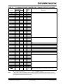
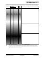
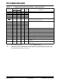
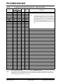
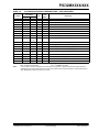
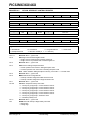
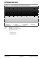
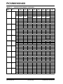
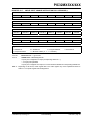
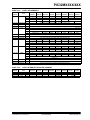
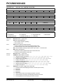
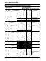
PIC32MX3XX/4XX USB – FEATURES
Trace
80
32/8
5/5/5
0
2
Yes
No
2/1/2
16
2
Yes Yes
64
80
128/32
5/5/5
4
2
Yes
No
2/2/2
16
2
Yes Yes
PIC32MX440F256H
64
80
256/32
5/5/5
4
2
Yes
No
2/1/2
16
2
Yes Yes
PIC32MX440F512H
64
80
512/32
5/5/5
4
2
Yes
No
2/1/2
16
2
Yes Yes
PIC32MX440F128L
100
80
128/32
5/5/5
4
2
Yes
No
2/2/2
16
2
Yes Yes
PIC32MX460F256L
100
80
256/32
5/5/5
4
2
Yes Yes
2/2/2
16
2
Yes Yes
PIC32MX460F512L
100
80
512/32
5/5/5
4
2
Yes Yes
2/2/2
16
2
Yes Yes
DS61143D-page 2
MHz
Program/Data
Memory
(KB)
Timers/
Capture/
Compare
Preliminary
EUART/
10-bit
SPI/
A/D (ch)
I2C™
JTAG
VREG
64
PIC32MX440F128H
Pins
PMP/PSP
Dedicated USB
DMA Channels
PIC32MX420F032H
Device
Comparators
Programmable
DMA Channels
USB
© 2008 Microchip Technology Inc.
PIC32MX3XX/4XX
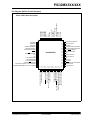
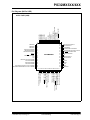
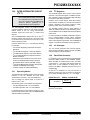
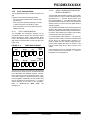
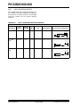
Pin Diagram (64-Pin General Purpose)
64
63
62
61
60
59
58
57
56
55
54
53
52
51
50
49
PMD4/RE4
PMD3/RE3
PMD2/RE2
PMD1/RE1
PMD0/RE0
RF1
RF0
ENVREG
VCAP/VDDCORE
CN16/RD7
CN15/RD6
PMRD/CN14/RD5
PMWR/OC5/IC5/CN13/RD4
OC4/RD3
OC3/RD2
OC2/RD1
64-Pin TQFP (General Purpose)
PMD5/RE5
PMD6/RE6
PMD7/RE7
PMA5/SCK2/CN8/RG6
PMA4/SDI2/CN9/RG7
PMA3/SDO2/CN10/RG8
MCLR
PMA2/SS2/CN11/RG9
VSS
VDD
C1IN+/AN5/CN7/RB5
C1IN-/AN4/CN6/RB4
C2IN+/AN3/CN5/RB3
C2IN-/AN2/SS1/CN4/RB2
PGC1/EMUC1/AN1/VREF-/CVREF-/CN3/RB1
2
3
4
5
6
7
8
9
10
11
12
45
PIC32MX3XXH
13
14
15
16
44
43
42
41
40
39
SOSCO/T1CK/CN0/RC14
SOSCI/CN1/RC13
OC1/RD0
IC4/PMCS1/PMA14/INT4/RD11
IC3/PMCS2/PMA15/INT3/RD10
IC2/U1CTS/INT2/RD9
IC1/RTCC/INT1/RD8
Vss
OSC2/CLKO/RC15
OSC1/CLKI/RC12
VDD
SCL1/RG2
38
37
36
35
SDA1/RG3
U1RTS/BCLK1/SCK1/INT0/RF6
34
33
U1RX/SDI1/RF2
U1TX/SDO1/RF3
PGC2/EMUC2/AN6/OCFA/RB6
PGD2/EMUD2/AN7/RB7
AVDD
AVSS
U2CTS/C1OUT/AN8/RB8
PMA7/C2OUT/AN9/RB9
TMS/CVREFOUT/PMA13/AN10/RB10
TDO/PMA12/AN11/RB11
VSS
VDD
TCK/PMA11/AN12/RB12
TDI/PMA10/AN13/RB13
PMALH/PMA1/U2RTS/BCLK2/AN14/RB14
PMALL/PMA0/AN15/OCFB/CN12/RB15
PMA9/U2RX/SDA2/CN17/RF4
PMA8/U2TX/SCL2/CN18/RF5
17
18
19
20
21
22
23
24
25
26
27
28
29
30
31
32
PGD1/EMUD1/PMA6/AN0/VREF+/CVREF+/CN2/RB0
48
47
46
1
© 2008 Microchip Technology Inc.
Preliminary
DS61143D-page 3
PIC32MX3XX/4XX
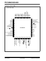
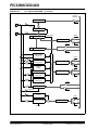
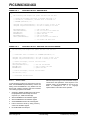
Pin Diagram (100-Pin General Purpose)
100
99
98
97
96
95
94
93
92
91
90
89
88
87
86
85
84
83
82
81
80
79
78
77
76
PMD4/RE4
PMD3/RE3
PMD2/RE2
TRD0/RG13
TRD1/RG12
TRD2/RG14
PMD1/RE1
PMD0/RE0
TRD3/RA7
TRCLK/RA6
PMD8/RG0
PMD9/RG1
PMD10/RF1
PMD11/RF0
ENVREG
VCAP/VDDCORE
PMD15/CN16/RD7
PMD14/CN15/RD6
PMRD/CN14/RD5
PMWR/OC5/CN13/RD4
PMD13/CN19/RD13
PMD12/IC5/RD12
OC4/RD3
OC3/RD2
OC2/RD1
100-Pin TQFP (General Purpose)
1
2
3
4
5
6
7
8
9
10
11
12
13
14
15
16
17
18
19
20
21
22
23
24
25
PIC32MX3XXL
75
74
73
72
71
70
69
68
67
66
65
64
63
62
61
60
59
58
57
56
55
54
53
52
51
VSS
SOSCO/T1CK/CN0/RC14
SOSCI/CN1/RC13
OC1/RD0
IC4/PMCS1/PMA14/RD11
IC3/PMCS2/PMA15/RD10
IC2/RD9
IC1/RTCC/RD8
INT4/RA15
INT3/RA14
VSS
OSC2/CLKO/RC15
OSC1/CLKI/RC12
VDD
TDO/RA5
TDI/RA4
SDA2/RA3
SCL2/RA2
SCL1/RG2
SDA1/RG3
SCK1/INT0/RF6
SDI1/RF7
SDO1/RF8
U1RX/RF2
U1TX/RF3
PGC2/EMUC2/AN6/OCFA/RB6
PGD2/EMUD2/AN7/RB7
PMA7/VREF-/CVREF-/RA9
PMA6/VREF+/CVREF+/RA10
AVDD
AVSS
C1OUT/AN8/RB8
C2OUT/AN9/RB9
CVREFOUT/PMA13/AN10/RB10
PMA12/AN11/RB11
VSS
VDD
TCK/RA1
U2RTS/BCLK2/RF13
U2CTS/RF12
PMA11/AN12/RB12
PMA10/AN13/RB13
PMALH/PMA1/AN14/RB14
PMALL/PMA0/AN15/OCFB/CN12/RB15
VSS
VDD
CN20/U1CTS/RD14
U1RTS/BCLK1/CN21/RD15
PMA9/U2RX/CN17/RF4
PMA8/U2TX/CN18/RF5
26
27
28
29
30
31
32
33
34
35
36
37
38
39
40
41
42
43
44
45
46
47
48
49
50
RG15
VDD
PMD5/RE5
PMD6/RE6
PMD7/RE7
T2CK/RC1
T3CK/RC2
T4CK/RC3
T5CK/RC4
PMA5/SCK2/CN8/RG6
PMA4/SDI2/CN9/RG7
PMA3/SDO2/CN10/RG8
MCLR
PMA2/SS2/CN11/RG9
VSS
VDD
TMS/RA0
INT1/RE8
INT2/RE9
C1IN+/AN5/CN7/RB5
C1IN-/AN4/CN6/RB4
C2IN+/AN3/CN5/RB3
C2IN-/AN2/SS1/CN4/RB2
PGC1/EMUC1/AN1/CN3/RB1
PGD1/EMUD1/AN0/CN2/RB0
DS61143D-page 4
Preliminary
© 2008 Microchip Technology Inc.
PIC32MX3XX/4XX
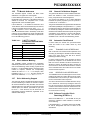
Pin Diagram (64-Pin USB)
64
63
62
61
60
59
58
57
56
55
54
53
52
51
50
49
PMD4/RE4
PMD3/RE3
PMD2/RE2
PMD1/RE1
PMD0/RE0
RF1
RF0
ENVREG
VCAP/VDDCORE
CN16/RD7
CN15/RD6
PMRD/CN14/RD5
PMWR/OC5/IC5/CN13/RD4
OC4/U1TX/RD3
OC3/U1RX/RD2
OC2/U1RTS/BCLK1/RD1
64-Pin TQFP (USB)
PMD5/RE5
PMD6/RE6
PMD7/RE7
PMA5/SCK2/CN8/RG6
PMA4/SDI2/CN9/RG7
PMA3/SDO2/CN10/RG8
MCLR
PMA2/SS2/CN11/RG9
VSS
VDD
VBUSON/C1IN+/AN5/CN7/RB5
C1IN-/AN4/CN6/RB4
C2IN+/AN3/CN5/RB3
C2IN-/AN2/CN4/RB2
PGC1/EMUC1/AN1/VREF-/CVREF-/CN3/RB1
2
3
4
5
6
7
8
9
10
11
12
48
SOSCO/T1CK/CN0/RC14
47
44
SOSCI/CN1/RC13
OC1/INT0/RD0
IC4/PMCS1/PMA14/INT4/RD11
IC3/PMCS2/PMA15/INT3/SCL1/RD10
43
IC2/U1CTS//INT2/SDA1/RD9
42
IC1/RTCC/INT1/RD8
41
Vss
OSC2/CLKO/RC15
46
45
PIC32MX4XXH
40
39
13
14
15
16
38
OSC1/CLKI/RC12
VDD
37
D+/RG2
36
35
D-/RG3
VUSB
34
33
VBUS
USBID/RF3
PGC2/EMUC2/AN6/OCFA/RB6
PGD2/EMUD2/AN7/RB7
AVDD
AVSS
U2CTS/C1OUT/AN8/RB8
PMA7/C2OUT/AN9/RB9
TMS/CVREFOUT/PMA13/AN10/RB10
TDO/PMA12/AN11/RB11
VSS
VDD
TCK/PMA11/AN12/RB12
TDI/PMA10/AN13/RB13
PMALH/PMA1/U2RTS/BCLK2/AN14/RB14
PMALL/PMA0/AN15/OCFB/CN12/RB15
PMA9/U2RX/SDA2/CN17/RF4
PMA8/U2TX/SCL2/CN18/RF5
17
18
19
20
21
22
23
24
25
26
27
28
29
30
31
32
PGD1/EMUD1/PMA6/AN0/VREF+/CVREF+/CN2/RB0
1
© 2008 Microchip Technology Inc.
Preliminary
DS61143D-page 5
PIC32MX3XX/4XX
Pin Diagram (100-Pin USB)
100
99
98
97
96
95
94
93
92
91
90
89
88
87
86
85
84
83
82
81
80
79
78
77
76
PMD4/RE4
PMD3/RE3
PMD2/RE2
TRD0/RG13
TRD1/RG12
TRD2/RG14
PMD1/RE1
PMD0/RE0
TRD3/RA7
TRCLK/RA6
PMD8/RG0
PMD9/RG1
PMD10/RF1
PMD11/RF0
ENVREG
VCAP/VDDCORE
PMD15/CN16/RD7
PMD14/CN15/RD6
PMRD/CN14/RD5
PMWR/OC5/CN13/RD4
PMD13/CN19/RD13
PMD12/IC5/RD12
OC4/RD3
OC3/RD2
OC2/RD1
100-Pin TQFP (USB)
1
2
3
4
5
6
7
8
9
10
11
12
13
14
15
16
17
18
19
20
21
22
23
24
25
PIC32MX4XXL
75
74
73
72
71
70
69
68
67
66
65
64
63
62
61
60
59
58
57
56
55
54
53
52
51
VSS
SOSCO/T1CK/CN0/RC14
SOSCI/CN1/RC13
SDO1/OC1/INT0/RD0
IC4/PMCS1/PMA14/RD11
IC3/SCKI/PMCS2/PMA15/RD10
IC2/SS1/RD9
IC1/RTCC/RD8
SDA1/INT4/RA15
SCL1/INT3/RA14
VSS
OSC2/CLKO/RC15
OSC1/CLKI/RC12
VDD
TDO/RA5
TDI/RA4
SDA2/RA3
SCL2/RA2
D+/RG2
D-/RG3
VUSB
VBUS
U1TX/RF8
U1RX/RF2
USBID/RF3
PGC2/EMUC2/AN6/OCFA/RB6
PGD2/EMUD2/AN7/RB7
PMA7/VREF-/CVREF-/RA9
PMA6/VREF+/CVREF+/RA10
AVDD
AVSS
C1OUT/AN8/RB8
C2OUT/AN9/RB9
CVREFOUT/PMA13/AN10/RB10
PMA12/AN11/RB11
VSS
VDD
TCK/RA1
U2RTS/BCLK2/RF13
U2CTS/RF12
PMA11/AN12/RB12
PMA10/AN13/RB13
PMALH/PMA1/AN14/RB14
PMALL/PMA0/AN15/OCFB/CN12/RB15
VSS
VDD
CN20/U1CTS/RD14
U1RTS/BCLK1/CN21/RD15
PMA9/U2RX/CN17/RF4
PMA8/U2TX/CN18/RF5
26
27
28
29
30
31
32
33
34
35
36
37
38
39
40
41
42
43
44
45
46
47
48
49
50
RG15
VDD
PMD5/RE5
PMD6/RE6
PMD7/RE7
T2CK/RC1
T3CK/RC2
T4CK/RC3
SDI1/T5CK/RC4
PMA5/SCK2/CN8/RG6
PMA4/SDI2/CN9/RG7
PMA3/SDO2/CN10/RG8
MCLR
PMA2/SS2/CN11/RG9
VSS
VDD
TMS/RA0
INT1/RE8
INT2/RE9
VBUSON/C1IN+/AN5/CN7/RB5
C1IN-/AN4/CN6/RB4
C2IN+/AN3/CN5/RB3
C2IN-/AN2/CN4/RB2
PGC1/EMUC1/AN1/CN3/RB1
PGD1/EMUD1/AN0/CN2/RB0
DS61143D-page 6
Preliminary
© 2008 Microchip Technology Inc.
PIC32MX3XX/4XX
Table of Contents
High-Performance 80 MHz MIPS-Based 32-Bit Flash Microcontroller 64/100-Pin General Purpose and USB..................................... 1
1.0 Device Overview .......................................................................................................................................................................... 9
2.0 PIC32MX MCU........................................................................................................................................................................... 33
3.0 Instruction Set ............................................................................................................................................................................ 47
4.0 Oscillators................................................................................................................................................................................... 53
5.0 Resets ........................................................................................................................................................................................ 83
6.0 Memory Organization ................................................................................................................................................................. 93
7.0 Flash Program Memory............................................................................................................................................................ 115
8.0 Interrupts .................................................................................................................................................................................. 125
9.0 Prefetch Cache......................................................................................................................................................................... 177
10.0 Direct Memory Access (DMA) Controller ................................................................................................................................. 197
11.0 USB On-The-Go....................................................................................................................................................................... 241
12.0 I/O Ports ................................................................................................................................................................................... 305
13.0 Timer1 ...................................................................................................................................................................................... 327
14.0 Timers 2, 3, 4, 5 ....................................................................................................................................................................... 339
15.0 Input Capture............................................................................................................................................................................ 355
16.0 Output Compare....................................................................................................................................................................... 365
17.0 Serial Peripheral Interface (SPI)............................................................................................................................................... 383
18.0 Inter-Integrated Circuit (I2C™) ................................................................................................................................................. 409
19.0 Universal Asynchronous Receiver Transmitter (UART) ........................................................................................................... 425
20.0 Parallel Master Port.................................................................................................................................................................. 439
21.0 Real-Time Clock and Calendar (RTCC)................................................................................................................................... 467
22.0 Analog-Digital Converter .......................................................................................................................................................... 489
23.0 Power Saving ........................................................................................................................................................................... 521
24.0 Comparator .............................................................................................................................................................................. 537
25.0 Comparator Reference............................................................................................................................................................. 549
26.0 Watchdog Timer ....................................................................................................................................................................... 555
27.0 Special Features ...................................................................................................................................................................... 565
28.0 Programming and Diagnostics ................................................................................................................................................. 577
29.0 Development Support............................................................................................................................................................... 589
30.0 Electrical Characteristics .......................................................................................................................................................... 593
31.0 Packaging Information.............................................................................................................................................................. 631
Index .................................................................................................................................................................................................. 639
Worldwide Sales and Service ............................................................................................................................................................ 642
© 2008 Microchip Technology Inc.
Preliminary
DS61143D-page 7
PIC32MX3XX/4XX
TO OUR VALUED CUSTOMERS
It is our intention to provide our valued customers with the best documentation possible to ensure successful use of your Microchip
products. To this end, we will continue to improve our publications to better suit your needs. Our publications will be refined and
enhanced as new volumes and updates are introduced.
If you have any questions or comments regarding this publication, please contact the Marketing Communications Department via
E-mail at [email protected] or fax the Reader Response Form in the back of this data sheet to (480) 792-4150. We
welcome your feedback.
Most Current Data Sheet
To obtain the most up-to-date version of this data sheet, please register at our Worldwide Web site at:
http://www.microchip.com
You can determine the version of a data sheet by examining its literature number found on the bottom outside corner of any page.
The last character of the literature number is the version number, (e.g., DS30000A is version A of document DS30000).
Errata
An errata sheet, describing minor operational differences from the data sheet and recommended workarounds, may exist for current
devices. As device/documentation issues become known to us, we will publish an errata sheet. The errata will specify the revision
of silicon and revision of document to which it applies.
To determine if an errata sheet exists for a particular device, please check with one of the following:
• Microchip’s Worldwide Web site; http://www.microchip.com
• Your local Microchip sales office (see last page)
When contacting a sales office, please specify which device, revision of silicon and data sheet (include literature number) you are
using.
Customer Notification System
Register on our web site at www.microchip.com to receive the most current information on all of our products.
DS61143D-page 8
Preliminary
© 2008 Microchip Technology Inc.
PIC32MX3XX/4XX
64/100-Pin General Purpose and USB,
32-bit Flash Microcontrollers
1.0
DEVICE OVERVIEW
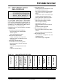
1.2
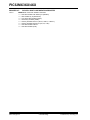
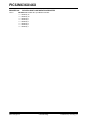
This document contains device specific information for
the following devices:
•
•
•
•
•
•
•
•
•
•
•
•
•
•
•
•
•
PIC32MX320F032H
PIC32MX320F064H
PIC32MX320F128H
PIC32MX320F128L
PIC32MX340F128H
PIC32MX340F128L
PIC32MX340F256H
PIC32MX340F512H
PIC32MX360F256L
PIC32MX360F512L
PIC32MX420F032H
PIC32MX440F256H
PIC32MX440F128H
PIC32MX440F128L
PIC32MX440F512H
PIC32MX460F256L
PIC32MX460F512L
Central to all PIC32MX3XX/4XX devices is the 32-bit
MIPS32 M4K CPU core, offering a wide range of
features, including the following:
Up to 1.56 DMIPS/MHz
32-bit Address and Data paths
32-bit Linear (program space) addressing
(2) thirty-two element 32-bit core register files
Single-cycle multiply and high-performance divide
unit for 32-bit integer math
• 16 and 32-bit instructions, optimized for
high-level languages, such as ‘C’.
1.3
Power-Saving Technology
All of the devices in the PIC32MX family incorporate a
range of features that can significantly reduce power
consumption during operation. Key features include:
• On-the-Fly Clock Switching: The device clock
can be changed under software control to any of
the four clock sources during operation.
• Instruction-Based Power-Saving Modes: The
microcontroller can suspend all operations, or
selectively shut down its core while leaving its
peripherals active, with a single instruction in
software.
1.4
Easy Migration
The PIC32MX family of microcontrollers was designed
to provide an easy migration path as the application
needs change.
The consistent pinout scheme used throughout the
entire family aids in migrating to the next larger device.
This is true when moving between devices with the
same pin count, or even jumping from 64-pin to 100-pin
devices.
The PIC32MX family is pin and peripheral compatible
with Microchip PIC24FJ128GA010 devices.
© 2008 Microchip Technology Inc.
32-BIT RISC ARCHITECTURE
•
•
•
•
•
This family introduces a new line of Microchip devices:
a 32-bit RISC microcontroller family with a broad
peripheral feature set and enhanced computational
performance. The PIC32MX3XX/4XX family offers a
new migration option for those high-performance applications which may be outgrowing their 16-bit platforms.
1.1
1.2.1
Core Features
Communications
The PIC32MX incorporates a range of serial communication peripherals to handle a range of application
requirements. All devices are equipped with two independent UARTs with built-in IrDA encoder/decoders.
There are also two independent SPI modules, and two
independent I2C modules that support both Master and
Slave modes of operation.
1.5
10-bit A/D Converter
The A/D Converter features 500 ksps maximum sample
rate. This configurable module incorporates a userselectable scan list and auto-convert functions to allow
acquisitions without processor intervention. Multiple A/D
trigger sources are user-selectable: timer event, external
pin, manual and auto-convert.
Preliminary
DS61143D-page 9
PIC32MX3XX/4XX
1.6
External Interface
A Parallel Master Port Parallel Slave Port enables 8/16bit parallel data communications in Master mode with
up to 16 address lines; 8-bit Slave modes are also
supported.
1.7
Real-Time Clock/Calendar
This module implements a full-featured clock and
calendar with alarm functions in hardware, freeing up
timer resources and program memory space for use of
the core application.
1.8
Oscillator Options and Features
All of the devices in the PIC32MX family offer four
different oscillator options, allowing users a range of
choices in developing application hardware. These
include:
• A Primary Oscillator (POSC) with two External
Crystal modes using crystals or ceramic
resonators.
• Two External Clock modes with selectable
peripheral bus clock output.
• A Fast Internal Oscillator (FRC) with a nominal
8 MHz output.
• On-board postscalers and/or PLL to provide clock
speeds ranging from 31 kHz to maximum
specified frequency.
• A Secondary Oscillator (SOSC) designed to
operate with an external 32.768 kHz crystal. This
oscillator can also be used with Timer1 and the
integrated RTCC.
• An Internal Low-Power RC oscillator (LPRC)
having a fixed 31 kHz output, which provides a
low-power option for timing-insensitive
applications.
The oscillator block also provides a stable reference
source for the user-controlled Fail-Safe Clock Monitor.
This option constantly monitors the main clock source
against a reference signal provided by the internal
oscillator and enables the controller to switch to the
internal oscillator, allowing for continued low-speed
operation or a safe application shutdown.
DS61143D-page 10
Preliminary
© 2008 Microchip Technology Inc.
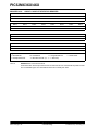
PIC32MX3XX/4XX
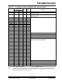
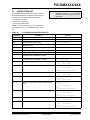
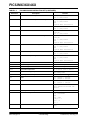
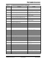
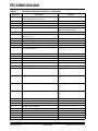
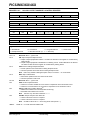
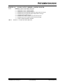
Device Features, Block Diagrams
and Pinout Tables
PIC32MX360F256L
PIC32MX360F512L
64K
128K
256K
128K
256K
512K
Data Memory (Bytes)
8K
16K
16K
32K
16K
32K
32K
DC – 40 MHz
DC – 80 MHz
Interrupt Sources/Vectors
I/O Ports
95 / 63
Ports B, C, D, E, F, G
Ports A, B, C, D, E, F, G
53
85
Total I/O Pins
DMA Channels
PIC32MX320F128L
32K
Operating Frequency
PIC32MX340F256H
Program Memory (Bytes)
Features
PIC32MX320F128H
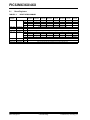
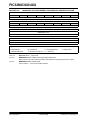
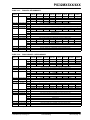
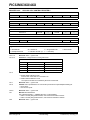
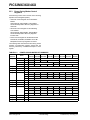
DEVICE FEATURES, BLOCK DIAGRAMS AND PINOUT TABLES
PIC32MX320F064H
TABLE 1-1:
PIC32MX320F032H
1.9
0
4
0
4
Timers:
Total number (16-bit)
5
32-bit (paired 16-bit)
2
32-bit core timer
1
Input Capture Channels
5
Output Compare/PWM
Channels
5
Input Change Interrupt
Notification
19
22
Serial Communications:
Enhanced UART
2
SPI (3-wire/4-wire)
2
2C™
2
I
Parallel Communications
(PMP/PSP)
Yes, 8-bit only
Yes, 8-bit/16-bit
JTAG Boundary Scan
Yes
JTAG Debug and Program
Yes
ICSP™ 2-Wire Debug and
Program
Yes
Instruction Trace
No
Yes
Hardware Break Points
6 Instruction, 2 Data
10-bit Analog-to-Digital
Module (input channels)
16
Analog Comparators
2
Internal LDO
Yes
Resets (and delays)
POR, BOR, MCLR, WDT, SWR (Software Reset), CM (Configuration Bit Mismatch)
(PWRT, OST, PLL Lock)
Instruction Support
MIPS32® Enhanced Architecture (Release 2)
MIPS16e™ Code Compression
Packages
© 2008 Microchip Technology Inc.
64-pin TQFP
Preliminary
100-pin TQFP
DS61143D-page 11
PIC32MX3XX/4XX
Operating Frequency
PIC32MX340F128L
Features
PIC32MX340F512H
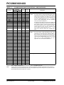
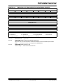
DEVICE FEATURES FOR THE PIC32MX3XXFXXX GENERAL PURPOSE FAMILY
PIC32MX340F128H
TABLE 1-2:
DC – 80 MHz
Program Memory (Bytes)
128K
512K
128K
Data Memory (Bytes)
32K
32K
32K
Interrupt Sources/Vectors
I/O Ports
Total I/O Pins
95 / 63
Ports B, C, D, E, F, G
Ports A, B, C, D, E, F, G
53
85
DMA Channels
4
Timers:
Total number (16-bit)
5
32-bit (paired 16-bit)
2
32-bit core timer
1
Input Capture Channels
5
Output Compare/PWM Channels
5
Input Change Interrupt Notification
19
22
Serial Communications:
Enhanced UART
2
SPI (3-wire/4-wire)
2
2C™
2
I
Parallel Communications (PMP/PSP)
Yes, 8-bit only
Yes, 8-bit/16-bit
JTAG Boundary Scan
Yes
JTAG Debug and Program
Yes
ICSP™ 2-Wire Debug and Program
Yes
Instruction Trace
No
Hardware Break Points
6 Instruction, 2 Data
10-bit Analog-to-Digital Module (input
channels)
16
Analog Comparators
2
Internal LDO
Yes
Resets (and delays)
POR, BOR, MCLR, WDT, SWR (Software Reset), CM (Configuration Bit
Mismatch)
(PWRT, OST, PLL Lock)
Instruction Support
MIPS32® Enhanced Architecture (Release 2)
MIPS16e™ Code Compression
Packages
DS61143D-page 12
64-pin TQFP
Preliminary
100-pin TQFP
© 2008 Microchip Technology Inc.
PIC32MX3XX/4XX
PIC32MX460F512L
512K
128K
256K
512K
32K
32K
32K
32K
DC – 80 MHz
Program Memory (Bytes)
32K
128K
256K
Data Memory (Bytes)
8K
32K
32K
Interrupt Sources / Vectors
95 / 63
I/O Ports
Total I/O Pins
DMA Channels
PIC32MX440F128L
PIC32MX440F512H
DC – 40
MHz
PIC32MX460F256L
Operating Frequency
PIC32MX440F256H
Features
PIC32MX440F128H
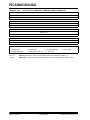
DEVICE FEATURES FOR THE PIC32MX4XXFXXX USB FAMILY
PIC32MX420F032H
TABLE 1-3:
Ports B, C, D, E, F, G
Ports A, B, C, D, E, F, G
51
83
0 + 2 USB
4 + 2 USB
Timers:
Total number (16-bit)
5
32-bit (from paired 16-bit
timers)
2
32-bit Core Timer
1
Input Capture Channels
5
Output Compare/PWM
Channels
5
Input Change Interrupt
Notification
19
22
Serial Communications:
Enhanced UART
SPI (3-wire/4-wire)
2
1
2
I2C™
Parallel Communications
(PMP/PSP)
2
Yes, 8-bit only
Yes, 8-bit/16-bit
JTAG Boundary Scan
Yes
JTAG Debug and Program
Yes
ICSP 2-wire Debug and
Program
Yes
Instruction Trace
No
Yes
Hardware Break Points:
6 Instruction, 2 Data
10-bit Analog-to-Digital
Module (input channels)
16
Analog Comparators
2
Internal LDO
Resets (and Delays)
Instruction Support
Yes
POR, BOR, MCLR, WDT, SWR (Software Reset), CM (Configuration Bit Mismatch)
(PWRT, OST, PLL Lock)
MIPS32 Enhanced Architecture (Release 2)
MIPS16e™ Code Compression
Packages
© 2008 Microchip Technology Inc.
64-pin TQFP
Preliminary
100-pin TQFP
DS61143D-page 13
PIC32MX3XX/4XX
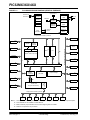
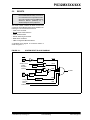
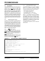
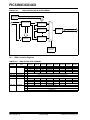
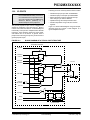
FIGURE 1-1:
PIC32MX3XX BLOCK DIAGRAM (GENERAL PURPOSE)
VDDCORE/VCAP
OSC2/CLKO
OSC1/CLKI
OSC/SOSC
Oscillators
Power-up
Timer
FRC/LPRC
Oscillators
ENVREG
Oscillator
Start-up Timer
Voltage
Regulator
PLL
Watchdog
Timer
SYSCLK
Timing
Generation
MCLR
Power-on
Reset
Precision
Band Gap
Reference
DIVIDERS
VDD, VSS
Brown-out
Reset(3)
PBCLK
Peripheral Bus Clocked by SYSCLK
CN1-22(1)
PORTA(1,4)
JTAG
BSCAN
Interrupt
Controller
PORTB
EJTAG
INT
DMAC(2)
ICD
32
MIPS32® M4K™ CPU Core
PORTC(1)
IS
DS
32
PORTD
32
32
32
32
(1)
Bus Matrix
Peripheral Bus Clocked by PBCLK
PWM
OC1-5
IC1-5
SPI1,2(1)
I2C1,2
32
32
32
32
PORTE(1)
Prefetch
Module(2)
Peripheral Bridge
Data RAM
PMP(1)
PORTF(1)
128
Flash
Controller
UART1,2
128-bit Wide
Program Flash Memory
PORTG(1)
Comparators
Peripheral Bus Clocked by PBCLK
Timer1
Note 1:
Timer2
Timer3
Timer4
Timer5
RTCC
10-bit ADC
Not all pins or features are implemented on all device pinout configurations. See Table 1-4 for I/O port pin descriptions.
2:
Some features are not available on certain devices.
3:
BOR functionality is provided when the on-board voltage regulator is enabled.
4:
PORTA is not present on 64-pin devices
DS61143D-page 14
Preliminary
© 2008 Microchip Technology Inc.
PIC32MX3XX/4XX
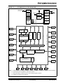
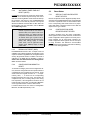
FIGURE 1-2:
PIC32MX4XX BLOCK DIAGRAM (USB)
VDDCORE/VCAP
OSC2/CLKO
OSC1/CLKI
OSC/SOSC
Oscillators
Power-up
Timer
FRC/LPRC
Oscillators
ENVREG
Voltage(1)
Regulator
Oscillator
Start-up Timer
PLL
Watchdog
Timer
PLL-USB
USBCLK
SYSCLK
Timing
Generation
MCLR
Power-on
Reset
Precision
Band Gap
Reference
DIVIDERS
VDD, VSS
Brown-out
Reset(2)
PBCLK
Peripheral Bus Clocked by SYSCLK
CN1-22(1)
PORTA(1,4)
Priority
Interrupt
Controller
JTAG
BSCAN
PORTB
EJTAG
INT
DMAC(1)
USB
ICD
32
MIPS M4K CPU Core
PORTC(1)
IS
DS
32
32
32
32
32
32
PORTD(1)
Bus Matrix
Peripheral Bus Clocked by PBCLK
PWM
OC 1,5
IC 1,5
SPI 1,2(1)
I2C 1,2
32
32
32
32
PORTE(1)
Pre-Fetch
Module(1)
Peripheral Bridge
Data RAM
PMP(1)
PORTF(1)
128
Flash
Controller
UART 1,2
128-bit wide
Program Flash Memory
PORTG(1)
Comparators
Peripheral Bus Clocked by PBCLK
Timer1
Note 1:
2:
Timer2
Timer3
Timer4
Timer5
RTCC
10-bit ADC
Not all pins or features are implemented on all device pinout configurations. See Table 1-5 for I/O port pin descriptions.
Some features are not available on certain device variants.
3:
BOR functionality is provided when the on-board voltage regulator is enabled.
4:
PORTA is not present on 64 pin devices
© 2008 Microchip Technology Inc.
Preliminary
DS61143D-page 15
PIC32MX3XX/4XX
TABLE 1-4:
PIC32MX3XX/4XX PINOUT DESCRIPTIONS – GENERAL PURPOSE
Pin Number
Function
I/O
64-pin
100-pin
Input
Buffer
AN0
16
25
I
ANA
AN1
15
24
I
ANA
AN2
14
23
I
ANA
AN3
13
22
I
ANA
AN4
12
21
I
ANA
AN5
11
20
I
ANA
AN6
17
26
I
ANA
AN7
18
27
I
ANA
AN8
21
32
I
ANA
AN9
22
33
I
ANA
Description
A/D Analog Inputs
AN10
23
34
I
ANA
AN11
24
35
I
ANA
AN12
27
41
I
ANA
AN13
28
42
I
ANA
AN14
29
43
I
ANA
AN15
30
44
I
ANA
AVDD
19
30
P
—
Positive Supply for Analog Modules
AVSS
20
31
P
—
Ground Reference for Analog Modules
BCLK1
35
48
O
—
UART1 IrDA® Baud Clock
BCLK2
29
39
O
—
C1IN-
12
21
I
ANA
Comparator 1 Negative Input
UART2 IrDA Baud Clock
C1IN+
11
20
I
ANA
Comparator 1 Positive Input
C1OUT
21
32
O
—
C2IN-
14
23
I
ANA
Comparator 2 Negative Input
Comparator 1 Output
Comparator 2 Positive Input
C2IN+
13
22
I
ANA
C2OUT
22
33
O
—
CLKI
39
63
I
ANA
CLKO
40
64
O
—
Legend:
Note:
Comparator 2 Output
Main Clock Input Connection
System Clock Output
TTL = TTL input buffer
ST = Schmitt Trigger input buffer
ANA = Analog level input/output
I2C™ = I2C/SMBus input buffer
In some cases, I/O pins are multiplexed with more than one peripheral. In general, the dominant output control of a
multiplexed I/O pin can be determined by the order of the peripheral output names assigned to a pin (read from left to
right). Multiplexed peripheral inputs have no priority.
DS61143D-page 16
Preliminary
© 2008 Microchip Technology Inc.
PIC32MX3XX/4XX
TABLE 1-4:
PIC32MX3XX/4XX PINOUT DESCRIPTIONS – GENERAL PURPOSE (CONTINUED)
Pin Number
I/O
Input
Buffer
74
I
ST
73
I
ST
16
25
I
ST
CN3
15
24
I
ST
CN4
14
23
I
ST
CN5
13
22
I
ST
CN6
12
21
I
ST
CN7
11
20
I
ST
CN8
4
10
I
ST
CN9
5
11
I
ST
CN10
6
12
I
ST
Function
64-pin
100-pin
CN0
48
CN1
47
CN2
CN11
8
14
I
ST
CN12
30
44
I
ST
CN13
52
81
I
ST
CN14
53
82
I
ST
CN15
54
83
I
ST
CN16
55
84
I
ST
CN17
31
49
I
ST
CN18
32
50
I
ST
CN19
—
80
I
ST
CN20
—
47
I
ST
CN21
—
48
I
ST
Description
Interrupt-on-Change Inputs
Interrupt-on-Change Inputs
CVREF-
15
28
I
ANA
CVREF+
16
29
I
ANA
Comparator Reference Voltage (Low) Input
Comparator Reference Voltage (High) Input
CVREFOUT
23
34
O
ANA
Comparator Voltage Reference Output
EMUC1
15
24
I/O
ST
In-Circuit Emulator Clock Input/Output
EMUD1
16
25
I/O
ST
In-Circuit Emulator Data Input/Output
EMUC2
17
26
I/O
ST
In-Circuit Emulator Clock Input/Output
EMUD2
18
27
I/O
ST
In-Circuit Emulator Data Input/Output
ENVREG
57
86
I
ST
Enable for On-Chip Voltage Regulator
IC1
42
68
I
ST
Input Capture Inputs
IC2
43
69
I
ST
IC3
44
70
I
ST
IC4
45
71
I
ST
IC5
52
79
I
ST
INT0
35
55
I
ST
INT1
42
18
I
ST
INT2
43
19
I
ST
INT3
44
66
I
ST
INT4
45
67
I
ST
MCLR
7
13
I
ST
Legend:
Note:
External Interrupt Inputs
Master Clear (Device Reset) Input. Bring this line low to cause a
Reset.
TTL = TTL input buffer
ST = Schmitt Trigger input buffer
ANA = Analog level input/output
I2C™ = I2C/SMBus input buffer
In some cases, I/O pins are multiplexed with more than one peripheral. In general, the dominant output control of a
multiplexed I/O pin can be determined by the order of the peripheral output names assigned to a pin (read from left to
right). Multiplexed peripheral inputs have no priority.
© 2008 Microchip Technology Inc.
Preliminary
DS61143D-page 17
PIC32MX3XX/4XX
TABLE 1-4:
PIC32MX3XX/4XX PINOUT DESCRIPTIONS – GENERAL PURPOSE (CONTINUED)
Pin Number
I/O
Input
Buffer
72
O
—
76
O
—
50
77
O
—
OC4
51
78
O
—
OC5
52
81
O
—
OCFA
17
26
I
ST
Output Compare Fault A Input
OCFB
30
44
I
ST
Output Compare Fault B Input
OSC1
39
63
I
ANA
Main Oscillator Input Connection
OSC2
40
64
O
ANA
Main Oscillator Output Connection.
PGC1
15
24
I/O
ST
In-Circuit Debugger and ICSP™ Programming Clock
PGD1
16
25
I/O
ST
In-Circuit Debugger and ICSP Programming Data
PGC2
17
26
I/O
ST
In-Circuit Debugger and ICSP™ Programming Clock
PGD2
18
27
I/O
ST
In-Circuit Debugger and ICSP Programming Data
PMALL
30
44
O
—
Parallel Master Port Address Latch Enable low-byte
(Multiplexed Master modes)
PMALH
29
43
O
—
Parallel Master Port Address Latch Enable high-byte
(Multiplexed Master modes)
PMA0
30
44
O
—
Parallel Master Port Address Bit 0 Input (Buffered Slave modes) and
Output (Master modes)
PMA1
29
43
O
—
Parallel Master Port Address Bit 1 Input (Buffered Slave modes) and
Output (Master modes)
Parallel Master Port Address (Demultiplexed Master modes)
Function
64-pin
100-pin
OC1
46
OC2
49
OC3
PMA2
8
14
O
—
PMA3
6
12
O
—
PMA4
5
11
O
—
PMA5
4
10
O
—
PMA6
16
29
O
—
PMA7
22
28
O
—
PMA8
32
50
O
—
PMA9
31
49
O
—
PMA10
28
42
O
—
PMA11
27
41
O
—
PMA12
24
35
O
—
PMA13
23
34
O
—
PMA14
45
71
O
—
PMA15
44
70
O
—
Description
Output Compare/PWM Outputs
PMCS1
45
71
O
—
Parallel Master Port Chip Select 1 Strobe
PMCS2
44
70
O
—
Parallel Master Port Chip Select 2 Strobe
Legend:
Note:
TTL = TTL input buffer
ST = Schmitt Trigger input buffer
ANA = Analog level input/output
I2C™ = I2C/SMBus input buffer
In some cases, I/O pins are multiplexed with more than one peripheral. In general, the dominant output control of a
multiplexed I/O pin can be determined by the order of the peripheral output names assigned to a pin (read from left to
right). Multiplexed peripheral inputs have no priority.
DS61143D-page 18
Preliminary
© 2008 Microchip Technology Inc.
PIC32MX3XX/4XX
TABLE 1-4:
PIC32MX3XX/4XX PINOUT DESCRIPTIONS – GENERAL PURPOSE (CONTINUED)
Pin Number
I/O
Input
Buffer
93
I/O
ST/TTL
94
I/O
ST/TTL
98
I/O
ST/TTL
Function
64-pin
100-pin
PMD0
60
PMD1
61
PMD2
62
PMD3
63
99
I/O
ST/TTL
PMD4
64
100
I/O
ST/TTL
PMD5
1
3
I/O
ST/TTL
PMD6
2
4
I/O
ST/TTL
PMD7
3
5
I/O
ST/TTL
PMD8
—
90
I/O
ST/TTL
PMD9
—
89
I/O
ST/TTL
PMD10
—
88
I/O
ST/TTL
PMD11
—
87
I/O
ST/TTL
PMD12
—
79
I/O
ST/TTL
PMD13
—
80
I/O
ST/TTL
PMD14
—
83
I/O
ST/TTL
ST/TTL
Description
Parallel Master Port Data (Demultiplexed Master mode) or
Address/Data (Multiplexed Master modes)
PMD15
—
84
I/O
PMENB
52
81
O
—
Parallel Master Port Enable Strobe (Master Mode 1)
PMRD
53
82
O
—
Parallel Master Port Read Strobe (Master Mode 2)
PMRD/PMWR
53
82
O
—
Parallel Master Port Read/Write Strobe (Master Mode 1)
PMWR
52
81
O
—
Parallel Master Port Write Strobe (Master Mode 2)
Legend:
Note:
TTL = TTL input buffer
ST = Schmitt Trigger input buffer
ANA = Analog level input/output
I2C™ = I2C/SMBus input buffer
In some cases, I/O pins are multiplexed with more than one peripheral. In general, the dominant output control of a
multiplexed I/O pin can be determined by the order of the peripheral output names assigned to a pin (read from left to
right). Multiplexed peripheral inputs have no priority.
© 2008 Microchip Technology Inc.
Preliminary
DS61143D-page 19
PIC32MX3XX/4XX
TABLE 1-4:
PIC32MX3XX/4XX PINOUT DESCRIPTIONS – GENERAL PURPOSE (CONTINUED)
Pin Number
I/O
Input
Buffer
17
I/O
ST
38
I/O
ST
—
58
I/O
ST
—
59
I/O
ST
RA4
—
60
I/O
ST
RA5
—
61
I/O
ST
RA6
—
91
I/O
ST
RA7
—
92
I/O
ST
Function
64-pin
100-pin
RA0
—
RA1
—
RA2
RA3
RA9
—
28
I/O
ST
RA10
—
29
I/O
ST
RA14
—
66
I/O
ST
RA15
—
67
I/O
ST
RB0
16
25
I/O
ST
RB1
15
24
I/O
ST
RB2
14
23
I/O
ST
RB3
13
22
I/O
ST
RB4
12
21
I/O
ST
RB5
11
20
I/O
ST
RB6
17
26
I/O
ST
RB7
18
27
I/O
ST
RB8
21
32
I/O
ST
RB9
22
33
I/O
ST
RB10
23
34
I/O
ST
RB11
24
35
I/O
ST
RB12
27
41
I/O
ST
RB13
28
42
I/O
ST
RB14
29
43
I/O
ST
RB15
30
44
I/O
ST
RC1
—
6
I/O
ST
RC2
—
7
I/O
ST
RC3
—
8
I/O
ST
RC4
—
9
I/O
ST
RC12
39
63
I/O
ST
RC13
47
73
I/O
ST
RC14
48
74
I/O
ST
RC15
40
64
I/O
ST
Legend:
Note:
Description
PORTA Digital I/O
Notes:
On 100-pin devices, JTAG program/debug port is multiplexed with port pins RA0, RA1, RA4 and RA5. At Reset,
these pins are controlled by the JTAG port. To use these
pins for general purpose I/O, the user’s application code
must clear JTAGEN (DDPCON<3>) bit = 0. To use these
pins for JTAG program/debug, the user’s application
code must maintain JTAGEN bit = 1.
On specific 100-pin devices, the instruction TRACE port
is multiplexed with PORTA pins RA6, RA7; PORTG pins
RG12, RG13 and RG14. At Power-on Reset, these pins
are general purpose I/O pins. To maintain these pins as
general purpose I/O pins, the user’s application code
must maintain TROEN (DDPCON<2>) bit = 0. To use
these pins as instruction TRACE pins, TROEN must be
set = 1.
PORTB Digital I/O
Note:
On 64-pin devices, JTAG program/debug port is multiplexed with port pins RB10, RB11, RB12 and RB13. At
Reset, these pins are controlled by the JTAG port. To use
these pins for general purpose I/O, the user’s application
code must clear JTAGEN (DDPCON<3>) bit = 0. To use
these pins for JTAG program/debug, the user’s
application code must maintain JTAGEN bit = 1.
PORTC Digital I/O
TTL = TTL input buffer
ST = Schmitt Trigger input buffer
ANA = Analog level input/output
I2C™ = I2C/SMBus input buffer
In some cases, I/O pins are multiplexed with more than one peripheral. In general, the dominant output control of a
multiplexed I/O pin can be determined by the order of the peripheral output names assigned to a pin (read from left to
right). Multiplexed peripheral inputs have no priority.
DS61143D-page 20
Preliminary
© 2008 Microchip Technology Inc.
PIC32MX3XX/4XX
TABLE 1-4:
PIC32MX3XX/4XX PINOUT DESCRIPTIONS – GENERAL PURPOSE (CONTINUED)
Pin Number
Function
I/O
64-pin
100-pin
Input
Buffer
RD0
46
72
I/O
ST
RD1
49
76
I/O
ST
RD2
50
77
I/O
ST
RD3
51
78
I/O
ST
RD4
52
81
I/O
ST
RD5
53
82
I/O
ST
RD6
54
83
I/O
ST
RD7
55
84
I/O
ST
RD8
42
68
I/O
ST
RD9
43
69
I/O
ST
RD10
44
70
I/O
ST
RD11
45
71
I/O
ST
RD12
—
79
I/O
ST
RD13
—
80
I/O
ST
RD14
—
47
I/O
ST
RD15
—
48
I/O
ST
RE0
60
93
I/O
ST
RE1
61
94
I/O
ST
RE2
62
98
I/O
ST
RE3
63
99
I/O
ST
RE4
64
100
I/O
ST
RE5
1
3
I/O
ST
RE6
2
4
I/O
ST
RE7
3
5
I/O
ST
RE8
—
18
I/O
ST
RE9
—
19
I/O
ST
RF0
58
87
I/O
ST
RF1
59
88
I/O
ST
RF2
34
52
I/O
ST
RF3
33
51
I/O
ST
RF4
31
49
I/O
ST
RF5
32
50
I/O
ST
RF6
35
55
I/O
ST
RF7
—
54
I/O
ST
RF8
—
53
I/O
ST
RF12
—
40
I/O
ST
—
39
I/O
ST
RF13
Legend:
Note:
Description
PORTD Digital I/O
PORTE Digital I/O
PORTF Digital I/O
TTL = TTL input buffer
ST = Schmitt Trigger input buffer
ANA = Analog level input/output
I2C™ = I2C/SMBus input buffer
In some cases, I/O pins are multiplexed with more than one peripheral. In general, the dominant output control of a
multiplexed I/O pin can be determined by the order of the peripheral output names assigned to a pin (read from left to
right). Multiplexed peripheral inputs have no priority.
© 2008 Microchip Technology Inc.
Preliminary
DS61143D-page 21
PIC32MX3XX/4XX
TABLE 1-4:
PIC32MX3XX/4XX PINOUT DESCRIPTIONS – GENERAL PURPOSE (CONTINUED)
Pin Number
Function
I/O
64-pin
100-pin
Input
Buffer
Description
RG0
—
90
I/O
ST
RG1
—
89
I/O
ST
PORTG Digital I/O
RG2
37
57
I/O
ST
RG3
36
56
I/O
ST
RG6
4
10
I/O
ST
RG7
5
11
I/O
ST
RG8
6
12
I/O
ST
RG9
8
14
I/O
ST
RG12
—
96
I/O
ST
RG13
—
97
I/O
ST
RG14
—
95
I/O
ST
RG15
—
1
I/O
ST
RTCC
42
68
O
—
Real-Time Clock Alarm Output
SCK1
35
55
O
—
SPI1 Serial Clock Output
Note:
On specific 100-pin devices, the Instruction TRACE port
is multiplexed with PORTA pins RA6, RA7; PORTG pins
RG12, RG13, and RG14. At power-on-reset, these pins
are general purpose I/O pins. To maintain these pins as
general purpose I/O pins, the user’s application code
must maintain TROEN (DDPCON<2>) bit = 0. To use
these pins as Instruction TRACE pins, TROEN must be
set = 1.
SCK2
4
10
I/O
ST
SPI2 Serial Clock Output
SCL1
37
57
I/O
I2C
I2C1 Synchronous Serial Clock Input/Output
SCL2
32
58
I/O
I2C
I2C2 Synchronous Serial Clock Input/Output.
SDA1
36
56
I/O
I2C
I2C1 Data Input/Output
2
SDA2
31
59
I/O
I C
I2C2 Data Input/Output
SDI1
34
54
I
ST
SPI1 Serial Data Input
SDI2
5
11
I
ST
SPI2 Serial Data Input
SDO1
33
53
O
—
SPI1 Serial Data Output
SDO2
6
12
O
—
SOSCI
47
73
I
ANA
Secondary Oscillator/Timer1 External Clock Input
SOSCO
48
74
O
ANA
Secondary Oscillator/Timer1 External Clock Output
SS1
14
23
I/O
ST
SS2
8
14
I/O
ST
Slave Select Input/Frame Select Output (SPI2)
T1CK
48
74
I
ST
Timer1 External Clock Input
T2CK
—
6
I
ST
Timer2 External Clock Input
T3CK
—
7
I
ST
Timer3 External Clock Input
T4CK
—
8
I
ST
Timer4 External Clock Input
T5CK
—
9
I
ST
Timer5 External Clock Input
TCK
27
38
I
ST
JTAG Test Clock/Programming Clock Input
TDI
28
60
I
ST
JTAG Test Data/Programming Data Input
TDO
24
61
O
—
JTAG Test Data Output
TMS
23
17
I
ST
JTAG Test Mode Select Input
TRCLK
—
91
O
—
Trace Clock
TRD0
—
97
O
—
Trace Data Bit 0
TRD1
—
96
O
—
Trace Data Bit 1
TRD2
—
95
O
—
Trace Data Bit 2
—
92
O
—
Trace Data Bit 3
TRD3
Legend:
Note:
SPI2 Serial Data Output
Slave Select Input/Frame Select Output (SPI1)
TTL = TTL input buffer
ST = Schmitt Trigger input buffer
ANA = Analog level input/output
I2C™ = I2C/SMBus input buffer
In some cases, I/O pins are multiplexed with more than one peripheral. In general, the dominant output control of a
multiplexed I/O pin can be determined by the order of the peripheral output names assigned to a pin (read from left to
right). Multiplexed peripheral inputs have no priority.
DS61143D-page 22
Preliminary
© 2008 Microchip Technology Inc.
PIC32MX3XX/4XX
TABLE 1-4:
PIC32MX3XX/4XX PINOUT DESCRIPTIONS – GENERAL PURPOSE (CONTINUED)
Pin Number
I/O
Input
Buffer
47
I
ST
Function
U1CTS
64-pin
100-pin
43
Description
UART1 Clear to Send Input
U1RTS
35
48
O
—
UART1 Request to Send Output
U1RX
34
52
I
ST
UART1 Receive
U1TX
33
51
O
—
UART1 Transmit Output
U2CTS
21
40
I
ST
UART2 Clear to Send Input
U2RTS
29
39
O
—
UART2 Request to Send Output
U2RX
31
49
I
ST
UART 2 Receive Input
32
50
O
—
UART2 Transmit Output
P
—
Positive Supply for Peripheral Digital Logic and I/O pins
U2TX
10, 26, 38 2, 16, 37,
46, 62
VDD
VDDCAP
56
85
P
—
External Filter Capacitor Connection (regulator enabled)
VDDCORE
56
85
P
—
Positive Supply for Microcontroller Core Logic (regulator disabled)
VREF-
15
28
I
ANA
A/D Reference Voltage (Low) Input
VREF+
16
29
I
ANA
A/D Reference Voltage (High) Input
VSS
9, 25, 41
15, 36,
45, 65, 75
P
—
Legend:
Note:
Ground Reference for Logic and I/O pins
TTL = TTL input buffer
ST = Schmitt Trigger input buffer
ANA = Analog level input/output
I2C™ = I2C/SMBus input buffer
In some cases, I/O pins are multiplexed with more than one peripheral. In general, the dominant output control of a
multiplexed I/O pin can be determined by the order of the peripheral output names assigned to a pin (read from left to
right). Multiplexed peripheral inputs have no priority.
© 2008 Microchip Technology Inc.
Preliminary
DS61143D-page 23
PIC32MX3XX/4XX
TABLE 1-5:
PIC32MX3XX/4XX PINOUT DESCRIPTIONS – USB
Pin Number
Function
I/O
64-pin
100-pin
Input
Buffer
AN0
16
25
I
ANA
AN1
15
24
I
ANA
AN2
14
23
I
ANA
AN3
13
22
I
ANA
AN4
12
21
I
ANA
AN5
11
20
I
ANA
AN6
17
26
I
ANA
AN7
18
27
I
ANA
AN8
21
32
I
ANA
AN9
22
33
I
ANA
Description
A/D Analog Inputs
AN10
23
34
I
ANA
AN11
24
35
I
ANA
AN12
27
41
I
ANA
AN13
28
42
I
ANA
AN14
29
43
I
ANA
AN15
30
44
I
ANA
AVDD
19
30
P
—
Positive Supply for Analog Modules
AVSS
20
31
P
—
Ground Reference for Analog Modules
BCLK1
49
48
O
—
UART1 IrDA® Baud Clock
BCLK2
29
39
O
—
UART2 IrDA® Baud Clock
C1IN-
12
21
I
ANA
Comparator 1 Negative Input
C1IN+
11
20
I
ANA
Comparator 1 Positive Input
C1OUT
21
32
O
—
C2IN-
14
23
I
ANA
Comparator 2 Negative Input
Comparator 1 Output
Comparator 2 Positive Input
C2IN+
13
22
I
ANA
C2OUT
22
33
O
—
CLKI
39
63
I
ANA
CLKO
40
64
O
—
Legend:
Note:
Comparator 2 Output
Main Clock Input Connection
System Clock Output
TTL = TTL input buffer
ST = Schmitt Trigger input buffer
ANA = Analog level input/output
I2C™ = I2C/SMBus input buffer
In some cases, I/O pins are multiplexed with more than one peripheral. In general, the dominant output control of a
multiplexed I/O pin can be determined by the order of the peripheral output names assigned to a pin (read from left to
right). Multiplexed peripheral inputs have no priority.
DS61143D-page 24
Preliminary
© 2008 Microchip Technology Inc.
PIC32MX3XX/4XX
TABLE 1-5:
PIC32MX3XX/4XX PINOUT DESCRIPTIONS – USB (CONTINUED)
Pin Number
I/O
Input
Buffer
74
I
ST
73
I
ST
16
25
I
ST
CN3
15
24
I
ST
CN4
14
23
I
ST
CN5
13
22
I
ST
CN6
12
21
I
ST
CN7
11
20
I
ST
CN8
4
10
I
ST
CN9
5
11
I
ST
CN10
6
12
I
ST
Function
64-pin
100-pin
CN0
48
CN1
47
CN2
CN11
8
14
I
ST
CN12
30
44
I
ST
CN13
52
81
I
ST
CN14
53
82
I
ST
CN15
54
83
I
ST
CN16
55
84
I
ST
CN17
31
49
I
ST
CN18
32
50
I
ST
CN19
—
80
I
ST
CN20
—
47
I
ST
CN21
—
48
I
ST
Description
Interrupt-on-Change Inputs
Interrupt-on-Change Inputs
CVREF-
15
28
I
ANA
CVREF+
16
29
I
ANA
Comparator Reference Voltage (Low) Input
Comparator Reference Voltage (High) Input
CVREFOUT
23
34
O
ANA
Comparator Voltage Reference Output
D+
37
57
I/O
ANA
USB D+
D-
36
56
I/O
ANA
EMUC1
15
24
I/O
ST
USB DIn-Circuit Emulator Clock Input/Output
EMUD1
16
25
I/O
ST
In-Circuit Emulator Data Input/Output
EMUC2
17
26
I/O
ST
In-Circuit Emulator Clock Input/Output
In-Circuit Emulator Data Input/Output
EMUD2
18
27
I/O
ST
ENVREG
57
86
I
ST
Enable for On-Chip Voltage Regulator
IC1
42
68
I
ST
Input Capture Inputs
IC2
43
69
I
ST
IC3
44
70
I
ST
IC4
45
71
I
ST
IC5
52
79
I
ST
Legend:
Note:
TTL = TTL input buffer
ST = Schmitt Trigger input buffer
ANA = Analog level input/output
I2C™ = I2C/SMBus input buffer
In some cases, I/O pins are multiplexed with more than one peripheral. In general, the dominant output control of a
multiplexed I/O pin can be determined by the order of the peripheral output names assigned to a pin (read from left to
right). Multiplexed peripheral inputs have no priority.
© 2008 Microchip Technology Inc.
Preliminary
DS61143D-page 25
PIC32MX3XX/4XX
TABLE 1-5:
PIC32MX3XX/4XX PINOUT DESCRIPTIONS – USB (CONTINUED)
Pin Number
I/O
Input
Buffer
72
I
ST
18
I
ST
43
19
I
ST
INT3
44
66
I
ST
INT4
45
67
I
ST
MCLR
7
13
I
ST
Master Clear (Device Reset) Input
Bring this line low to cause a Reset.
OC1
46
72
O
—
Output Compare/PWM Outputs
OC2
49
76
O
—
OC3
50
77
O
—
OC4
51
78
O
—
OC5
52
81
O
—
OCFA
17
26
I
ST
Function
64-pin
100-pin
INT0
46
INT1
42
INT2
Description
External Interrupt Inputs
Output Compare Fault A Input
OCFB
30
44
I
ST
OSC1
39
63
I
ANA
Main Oscillator Input Connection
OSC2
40
64
O
ANA
Main Oscillator Output Connection
PGC1
15
24
I/O
ST
In-Circuit Debugger and ICSP™ Programming Clock
PGD1
16
25
I/O
ST
In-Circuit Debugger and ICSP Programming Data
PGC2
17
26
I/O
ST
In-Circuit Debugger and ICSP™ Programming Clock
PGD2
18
27
I/O
ST
In-Circuit Debugger and ICSP Programming Data
PMALL
30
44
O
—
Parallel Master Port Address Latch Enable low-byte (Multiplexed Master modes)
PMALH
29
43
O
—
Parallel Master Port Address Latch Enable high-byte (Multiplexed
Master modes)
Legend:
Note:
Output Compare Fault B Input
TTL = TTL input buffer
ST = Schmitt Trigger input buffer
ANA = Analog level input/output
I2C™ = I2C/SMBus input buffer
In some cases, I/O pins are multiplexed with more than one peripheral. In general, the dominant output control of a
multiplexed I/O pin can be determined by the order of the peripheral output names assigned to a pin (read from left to
right). Multiplexed peripheral inputs have no priority.
DS61143D-page 26
Preliminary
© 2008 Microchip Technology Inc.
PIC32MX3XX/4XX
TABLE 1-5:
PIC32MX3XX/4XX PINOUT DESCRIPTIONS – USB (CONTINUED)
Pin Number
I/O
Input
Buffer
44
O
—
Parallel Master Port Address Bit 0 Input (Buffered Slave modes) and
Output (Master modes)
43
O
—
Parallel Master Port Address Bit 1 Input (Buffered Slave modes) and
Output (Master modes)
Parallel Master Port Address (Demultiplexed Master modes)
Function
64-pin
100-pin
PMA0
30
PMA1
29
PMA2
8
14
O
—
PMA3
6
12
O
—
PMA4
5
11
O
—
PMA5
4
10
O
—
PMA6
16
29
O
—
PMA7
22
28
O
—
PMA8
32
50
O
—
PMA9
31
49
O
—
PMA10
28
42
O
—
PMA11
27
41
O
—
PMA12
24
35
O
—
PMA13
23
34
O
—
Description
PMA14
45
71
O
—
Address bit 14
PMA15
44
70
O
—
Address bit 15
PMCS1
45
71
O
—
Parallel Master Port Chip Select 1 Strobe
PMCS2
44
70
O
—
Parallel Master Port Chip Select 2 Strobe
PMD0
60
93
I/O
ST/TTL
PMD1
61
94
I/O
ST/TTL
PMD2
62
98
I/O
ST/TTL
PMD3
63
99
I/O
ST/TTL
PMD4
64
100
I/O
ST/TTL
PMD5
1
3
I/O
ST/TTL
PMD6
2
4
I/O
ST/TTL
PMD7
3
5
I/O
ST/TTL
PMD8
—
90
I/O
ST/TTL
PMD9
—
89
I/O
ST/TTL
PMD10
—
88
I/O
ST/TTL
PMD11
—
87
I/O
ST/TTL
PMD12
—
79
I/O
ST/TTL
PMD13
—
80
I/O
ST/TTL
PMD14
—
83
I/O
ST/TTL
PMD15
—
84
I/O
ST/TTL
Parallel Master Port Data (Demultiplexed Master mode) or
Address/Data (Multiplexed Master modes)
PMENB
52
81
O
—
Parallel Master Port Enable Strobe (Master mode 1)
PMRD
53
82
O
—
Parallel Master Port Read Strobe (Master mode 2)
PMRD/PMWR
53
82
O
—
Parallel Master Port Read/Write Strobe (Master mode 1)
PMWR
52
81
O
—
Parallel Master Port Write Strobe (Master mode 2)
Legend:
Note:
TTL = TTL input buffer
ST = Schmitt Trigger input buffer
ANA = Analog level input/output
I2C™ = I2C/SMBus input buffer
In some cases, I/O pins are multiplexed with more than one peripheral. In general, the dominant output control of a
multiplexed I/O pin can be determined by the order of the peripheral output names assigned to a pin (read from left to
right). Multiplexed peripheral inputs have no priority.
© 2008 Microchip Technology Inc.
Preliminary
DS61143D-page 27
PIC32MX3XX/4XX
TABLE 1-5:
PIC32MX3XX/4XX PINOUT DESCRIPTIONS – USB (CONTINUED)
Pin Number
I/O
Input
Buffer
17
I/O
ST
38
I/O
ST
—
58
I/O
ST
—
59
I/O
ST
RA4
—
60
I/O
ST
RA5
—
61
I/O
ST
RA6
—
91
I/O
ST
RA7
—
92
I/O
ST
Function
64-pin
100-pin
RA0
—
RA1
—
RA2
RA3
RA9
—
28
I/O
ST
RA10
—
29
I/O
ST
RA14
—
66
I/O
ST
RA15
—
67
I/O
ST
RB0
16
25
I/O
ST
RB1
15
24
I/O
ST
RB2
14
23
I/O
ST
RB3
13
22
I/O
ST
RB4
12
21
I/O
ST
RB5
11
20
I/O
ST
RB6
17
26
I/O
ST
RB7
18
27
I/O
ST
RB8
21
32
I/O
ST
RB9
22
33
I/O
ST
RB10
23
34
I/O
ST
RB11
24
35
I/O
ST
RB12
27
41
I/O
ST
RB13
28
42
I/O
ST
RB14
29
43
I/O
ST
RB15
30
44
I/O
ST
RC1
—
6
I/O
ST
RC2
—
7
I/O
ST
RC3
—
8
I/O
ST
RC4
—
9
I/O
ST
RC12
39
63
I/O
ST
RC13
47
73
I/O
ST
RC14
48
74
I/O
ST
RC15
40
64
I/O
ST
Legend:
Note:
Description
PORTA Digital I/O
Notes:
On 100-pin devices, JTAG program/debug port is multiplexed with port pins RA0, RA1, RA4 and RA5. At Reset,
these pins are controlled by the JTAG port. To use these
pins for general purpose I/O, the user’s application code
must clear JTAGEN (DDPCON<3>) bit = 0. To use these
pins for JTAG program/debug, the user’s application
code must maintain JTAGEN bit = 1.
On specific 100-pin devices, the instruction TRACE port
is multiplexed with PORTA pins RA6, RA7; PORTG pins
RG12, RG13 and RG14. At Power-on Reset, these pins
are general purpose I/O pins. To maintain these pins as
general purpose I/O pins, the user’s application code
must maintain TROEN (DDPCON<2>) bit = 0. To use
these pins as instruction TRACE pins, TROEN must be
set = 1.
PORTB Digital I/O
Note:
On 64-pin devices, JTAG program/debug port is multiplexed with port pins RB10, RB11, RB12 and RB13. At
Reset, these pins are controlled by the JTAG port. To use
these pins for general purpose I/O, the user’s application
code must clear JTAGEN (DDPCON<3>) bit = 0. To use
these pins for JTAG program/debug, the user’s
application code must maintain JTAGEN bit = 1.
PORTC Digital I/O
TTL = TTL input buffer
ST = Schmitt Trigger input buffer
ANA = Analog level input/output
I2C™ = I2C/SMBus input buffer
In some cases, I/O pins are multiplexed with more than one peripheral. In general, the dominant output control of a
multiplexed I/O pin can be determined by the order of the peripheral output names assigned to a pin (read from left to
right). Multiplexed peripheral inputs have no priority.
DS61143D-page 28
Preliminary
© 2008 Microchip Technology Inc.
PIC32MX3XX/4XX
TABLE 1-5:
PIC32MX3XX/4XX PINOUT DESCRIPTIONS – USB (CONTINUED)
Pin Number
Function
I/O
64-pin
100-pin
Input
Buffer
RD0
46
72
I/O
ST
RD1
49
76
I/O
ST
RD2
50
77
I/O
ST
RD3
51
78
I/O
ST
RD4
52
81
I/O
ST
RD5
53
82
I/O
ST
RD6
54
83
I/O
ST
RD7
55
84
I/O
ST
RD8
42
68
I/O
ST
RD9
43
69
I/O
ST
RD10
44
70
I/O
ST
RD11
45
71
I/O
ST
RD12
—
79
I/O
ST
RD13
—
80
I/O
ST
RD14
—
47
I/O
ST
RD15
—
48
I/O
ST
RE0
60
93
I/O
ST
RE1
61
94
I/O
ST
RE2
62
98
I/O
ST
RE3
63
99
I/O
ST
RE4
64
100
I/O
ST
RE5
1
3
I/O
ST
RE6
2
4
I/O
ST
RE7
3
5
I/O
ST
RE8
—
18
I/O
ST
RE9
—
19
I/O
ST
RF0
58
87
I/O
ST
RF1
59
88
I/O
ST
RF2
—
52
I/O
ST
RF3
33
51
I/O
ST
RF4
31
49
I/O
ST
RF5
32
50
I/O
ST
RF8
—
53
I/O
ST
RF12
—
40
I/O
ST
—
39
I/O
ST
RF13
Legend:
Note:
Description
PORTD Digital I/O
PORTE Digital I/O
PORTF Digital I/O
TTL = TTL input buffer
ST = Schmitt Trigger input buffer
ANA = Analog level input/output
I2C™ = I2C/SMBus input buffer
In some cases, I/O pins are multiplexed with more than one peripheral. In general, the dominant output control of a
multiplexed I/O pin can be determined by the order of the peripheral output names assigned to a pin (read from left to
right). Multiplexed peripheral inputs have no priority.
© 2008 Microchip Technology Inc.
Preliminary
DS61143D-page 29
PIC32MX3XX/4XX
TABLE 1-5:
PIC32MX3XX/4XX PINOUT DESCRIPTIONS – USB (CONTINUED)
Pin Number
Function
I/O
64-pin
100-pin
Input
Buffer
RG0
—
90
I/O
ST
RG1
—
89
I/O
ST
RG2
37
57
I/O
ST
RG3
36
56
I/O
ST
RG6
4
10
I/O
ST
RG7
5
11
I/O
ST
RG8
6
12
I/O
ST
RG9
8
14
I/O
ST
RG12
—
96
I/O
ST
RG13
—
97
I/O
ST
RG14
—
95
I/O
ST
RG15
—
1
I/O
ST
RTCC
42
68
O
—
SCK1
—
70
O
—
Description
PORTG Digital I/O
Note:
On specific 100-pin devices, the instruction TRACE port
is multiplexed with PORTA pins RA6, RA7; PORTG pins
RG12, RG13 and RG14. At Power-on Reset, these pins
are general purpose I/O pins. To maintain these pins as
general purpose I/O pins, the user’s application code
must maintain TROEN (DDPCON<2>) bit = 0. To use
these pins as instruction TRACE pins, TROEN must be
set = 1.
Real-Time Clock Alarm Output
SCK2
4
10
I/O
ST
SPI2 Serial Clock Output
SCL1
44
66
I/O
I2C
I2C1 Synchronous Serial Clock Input/Output
SCL2
32
58
I/O
I2C
I2C2 Synchronous Serial Clock Input/Output
SDA1
43
67
I/O
I2C
I2C1 Data Input/Output
2
I2C2 Data Input/Output
SDA2
31
59
I/O
I C
SDI1
—
9
I
ST
SDI2
5
11
I
ST
SDO1
—
72
O
—
SPI2 Serial Data Input
SDO2
6
12
O
—
SOSCI
47
73
I
ANA
Secondary Oscillator/Timer1 External Clock Input
SOSCO
48
74
O
ANA
Secondary Oscillator/Timer1 External Clock Output
SS1
—
69
I/O
ST
SS2
8
14
I/O
ST
Slave Select Input/Frame Select Output (SPI2)
T1CK
48
74
I
ST
Timer1 External Clock Input
T2CK
—
6
I
ST
Timer2 External Clock Input
T3CK
—
7
I
ST
Timer3 External Clock Input
T4CK
—
8
I
ST
Timer4 External Clock Input
T5CK
—
9
I
ST
Timer5 External Clock Input
TCK
27
38
I
ST
JTAG Test Clock/Programming Clock Input
TDI
28
60
I
ST
JTAG Test Data/Programming Data Input
TDO
24
61
O
—
JTAG Test Data Output
TMS
23
17
I
ST
JTAG Test Mode Select Input
TRCLK
—
91
O
—
Trace Clock
TRD0
—
97
O
—
Trace Data Bit 0
TRD1
—
96
O
—
Trace Data Bit 1
TRD2
—
95
O
—
Trace Data Bit 2
—
92
O
—
Trace Data Bit 3
TRD3
Legend:
Note:
SPI2 Serial Data Output
Slave Select Input/Frame Select Output (SPI1)
TTL = TTL input buffer
ST = Schmitt Trigger input buffer
ANA = Analog level input/output
I2C™ = I2C/SMBus input buffer
In some cases, I/O pins are multiplexed with more than one peripheral. In general, the dominant output control of a
multiplexed I/O pin can be determined by the order of the peripheral output names assigned to a pin (read from left to
right). Multiplexed peripheral inputs have no priority.
DS61143D-page 30
Preliminary
© 2008 Microchip Technology Inc.
PIC32MX3XX/4XX
TABLE 1-5:
PIC32MX3XX/4XX PINOUT DESCRIPTIONS – USB (CONTINUED)
Pin Number
I/O
Input
Buffer
47
I
ST
Function
U1CTS
64-pin
100-pin
43
Description
UART1 Clear to Send Input
U1RTS
49
48
O
—
UART1 Request to Send Output
U1RX
50
52
I
ST
UART1 Receive
U1TX
51
53
O
—
UART1 Transmit Output
U2CTS
21
40
I
ST
UART2 Clear to Send Input
U2RTS
29
39
O
—
UART2 Request to Send Output
U2RX
31
49
I
ST
UART 2 Receive Input
U2TX
32
50
O
—
UART2 Transmit Output
VDD
10, 26, 38
2, 16, 37,
46, 62
P
—
Positive Supply for Peripheral Digital Logic and I/O pins
VDDCAP
56
85
P
—
External Filter Capacitor Connection (regulator enabled)
VDDCORE
56
85
P
—
Positive Supply for Microcontroller Core Logic (regulator disabled)
VREF-
15
28
I
ANA
A/D and Comparator Reference Voltage (Low) Input
VREF+
16
29
I
ANA
A/D and Comparator Reference Voltage (High) Input
VSS
9, 25, 41
15, 36,
45, 65, 75
P
—
VBUS
34
54
I
ANA
VUSB
35
55
P
—
Ground Reference for Logic and I/O pins
USB Bus Power Monitor
USB Internal Transceiver Supply
VBUSON
11
20
O
—
USB Host and OTG Bus Power Control Output
USBID
33
51
I
ST
USB OTG ID Detect
Legend:
Note:
TTL = TTL input buffer
ST = Schmitt Trigger input buffer
ANA = Analog level input/output
I2C™ = I2C/SMBus input buffer
In some cases, I/O pins are multiplexed with more than one peripheral. In general, the dominant output control of a
multiplexed I/O pin can be determined by the order of the peripheral output names assigned to a pin (read from left to
right). Multiplexed peripheral inputs have no priority.
© 2008 Microchip Technology Inc.
Preliminary
DS61143D-page 31
PIC32MX3XX/4XX
NOTES:
DS61143D-page 32
Preliminary
© 2008 Microchip Technology Inc.
PIC32MX3XX/4XX
2.0
Note:
PIC32MX MCU
This data sheet summarizes the features of
the PIC32MX3XX/4XX Family of devices. It
is not intended to be a comprehensive reference source. Refer to the “PIC32MX Family
Reference Manual” (DS61132) for a detailed
description of the PIC32MX mcu.
Resources for the MIPS32® M4K®
Processor
Core
are
available
at
www.mips.com/products/cores/32-bit-cores/
mips32-m4k/#.
The MCU module is the heart of the PIC32MX3XX/4XX
Family processor. The MCU fetches instructions,
decodes each instruction, fetches source operands,
executes each instruction and writes the results of
instruction execution to the proper destinations.
2.1
Features
• Autonomous Multiply/Divide Unit
- Maximum issue rate of one 32x16 multiply
per clock
- Maximum issue rate of one 32x32 multiply
every other clock
- Early-in iterative divide. Minimum 11 and
maximum 34 clock latency (dividend (rs) sign
extension-dependent)
• Power Control
- Minimum frequency: 0 MHz
- Low-Power mode (triggered by WAIT
instruction)
- Extensive use of local gated clocks
• EJTAG Debug and Instruction Trace
- Support for single stepping
- Virtual instruction and data address/value
breakpoints
- PC tracing with trace compression
• 5-stage pipeline
• 32-bit Address and Data Paths
• MIPS32 Enhanced Architecture (Release 2)
- Multiply-Accumulate and Multiply-Subtract
Instructions
- Targeted Multiply Instruction
- Zero/One Detect Instructions
- WAIT Instruction
- Conditional Move Instructions (MOVN, MOVZ)
- Vectored interrupts
- Programmable exception vector base
- Atomic interrupt enable/disable
- GPR shadow registers to minimize latency
for interrupt handlers
- Bit field manipulation instructions
• MIPS16e™ Code Compression
- 16-bit encoding of 32-bit instructions to
improve code density
- Special PC-relative instructions for efficient
loading of addresses and constants
- SAVE & RESTORE macro instructions for
setting up and tearing down stack frames
within subroutines
- Improved support for handling 8 and 16-bit
data types
• Simple Fixed Mapping Translation (FMT)
mechanism
• Simple Dual Bus Interface
- Independent 32-bit address and data busses
- Transactions can be aborted to improve
interrupt latency
© 2008 Microchip Technology Inc.
Preliminary
DS61143D-page 33
PIC32MX3XX/4XX
2.2
Architecture Overview
The PIC32MX3XX/4XX Family core contains several
logic blocks working together in parallel, providing an
efficient high performance computing engine. The
following blocks are included with the core:
• Execution Unit
• Multiply/Divide Unit (MDU)
• System Control Coprocessor (CP0)
• Fixed Mapping Translation (FMT)
• Dual Internal Bus interfaces
• Power Management
• MIPS16e Support
• Enhanced JTAG (EJTAG) Controller
MCU BLOCK DIAGRAM
EJTAG
Trace
TAP
MDU
Execution
Core
(RF/ALU/Shift)
FMT
Bus Interface
System
Coprocessor
DS61143D-page 34
Trace I/F
Off-Chip
Debug I/F
Dual Bus I/F
Bus Matrix
FIGURE 2-1:
Power
Mgmt
Preliminary
© 2008 Microchip Technology Inc.
PIC32MX3XX/4XX
2.2.1
EXECUTION UNIT
2.2.2
The PIC32MX3XX/4XX Family core execution unit
implements a load/store architecture with single-cycle
ALU operations (logical, shift, add, subtract) and an
autonomous multiply/divide unit. The core contains
thirty-two 32-bit general purpose registers used for
integer operations and address calculation. One
additional register file shadow set (containing thirty-two
registers) is added to minimize context switching
overhead during interrupt/exception processing. The
register file consists of two read ports and one write
port and is fully bypassed to minimize operation latency
in the pipeline.
The execution unit includes:
• 32-bit adder used for calculating the data address
• Address unit for calculating the next instruction
address
• Logic for branch determination and branch target
address calculation
• Load aligner
• Bypass multiplexers used to avoid stalls when
executing instructions streams where data
producing instructions are followed closely by
consumers of their results
• Leading Zero/One detect unit for implementing the
CLZ and CLO instructions
• Arithmetic Logic Unit (ALU) for performing bitwise
logical operations
• Shifter and Store Aligner
MULTIPLY/DIVIDE UNIT (MDU)
The PIC32MX3XX/4XX Family core includes a
multiply/divide unit (MDU) that contains a separate
pipeline for multiply and divide operations. This pipeline
operates in parallel with the integer unit (IU) pipeline
and does not stall when the IU pipeline stalls. This
allows MDU operations to be partially masked by
system stalls and/or other integer unit instructions.
The high-performance MDU consists of a 32x16 booth
recoded multiplier, result/accumulation registers (HI
and LO), a divide state machine, and the necessary
multiplexers and control logic. The first number shown
(‘32’ of 32x16) represents the rs operand. The second
number (‘16’ of 32x16) represents the rt operand. The
PIC32MX core only checks the value of the latter (rt)
operand to determine how many times the operation
must pass through the multiplier. The 16x16 and 32x16
operations pass through the multiplier once. A 32x32
operation passes through the multiplier twice.
The MDU supports execution of one 16x16 or 32x16
multiply operation every clock cycle; 32x32 multiply
operations can be issued every other clock cycle.
Appropriate interlocks are implemented to stall the
issuance of back-to-back 32x32 multiply operations.
The multiply operand size is automatically determined
by logic built into the MDU.
Divide operations are implemented with a simple 1 bit
per clock iterative algorithm. An early-in detection
checks the sign extension of the dividend (rs) operand.
If rs is 8 bits wide, 23 iterations are skipped. For a 16bit-wide rs, 15 iterations are skipped, and for a 24-bitwide rs, 7 iterations are skipped. Any attempt to issue
a subsequent MDU instruction while a divide is still
active causes an IU pipeline stall until the divide
operation is completed.
Table 2-1 lists the repeat rate (peak issue rate of cycles
until the operation can be reissued) and latency
(number of cycles until a result is available) for the
PIC32MX core multiply and divide instructions. The
approximate latency and repeat rates are listed in
terms of pipeline clocks.
© 2008 Microchip Technology Inc.
Preliminary
DS61143D-page 35
PIC32MX3XX/4XX
TABLE 2-1:
PIC32MX3XX/4XX FAMILY CORE HIGH-PERFORMANCE INTEGER
MULTIPLY/DIVIDE UNIT LATENCIES AND REPEAT RATES
Opcode
Operand Size (mul rt) (div rs)
Latency
Repeat Rate
MULT/MULTU, MADD/MADDU,
MSUB/MSUBU
16 bits
1
1
32 bits
2
2
MUL
16 bits
2
1
DIV/DIVU
32 bits
3
2
8 bits
12
11
16 bits
19
18
24 bits
26
25
32 bits
33
32
The MIPS architecture defines that the result of a
multiply or divide operation be placed in the HI and LO
registers. Using the Move-From-HI (MFHI) and MoveFrom-LO (MFLO) instructions, these values can be
transferred to the general purpose register file.
In addition to the HI/LO targeted operations, the
MIPS32 architecture also defines a multiply instruction,
MUL, which places the least significant results in the
primary register file instead of the HI/LO register pair.
By avoiding the explicit MFLO instruction, required
when using the LO register, and by supporting multiple
destination
registers,
the
throughput
of
multiply-intensive operations is increased.
Two other instructions, multiply-add (MADD) and
multiply-subtract (MSUB), are used to perform the
multiply-accumulate and multiply-subtract operations.
The MADD instruction multiplies two numbers and then
adds the product to the current contents of the HI and
LO registers. Similarly, the MSUB instruction multiplies
two operands and then subtracts the product from the
HI and LO registers. The MADD and MSUB operations
are commonly used in DSP algorithms.
DS61143D-page 36
Preliminary
© 2008 Microchip Technology Inc.
PIC32MX3XX/4XX
2.2.3
SYSTEM CONTROL
COPROCESSOR (CP0)
In the MIPS architecture, CP0 is responsible for the
virtual-to-physical address translation, the exception
control system, the processor’s diagnostics capability,
the operating modes (kernel, user, and debug), and
whether interrupts are enabled or disabled.
Configuration information, such as presence of options
like MIPS16e, is also available by accessing the CP0
registers, listed in Table 2-2.
TABLE 2-2:
COPROCESSOR 0 REGISTERS
Register Register
Number Name
Function
0-6
Reserved
Reserved in the PIC32MX3XX/4XX Family core
7
HWREna
Enables access via the RDHWR instruction to selected hardware registers
8
BadVAddr(1)
Reports the address for the most recent address-related exception
9
Count(1)
Processor cycle count
10
Reserved
Reserved in the PIC32MX3XX/4XX Family core
11
Compare(1)
Timer interrupt control
12
Status(1)
Processor status and control
12
IntCtl(1)
Interrupt system status and control
12
SRSCtl(1)
Shadow register set status and control
12
SRSMap(1)
Provides mapping from vectored interrupt to a shadow set
13
Cause(1)
Cause of last general exception
(1)
14
EPC
Program counter at last exception
15
PRId
Processor identification and revision
15
EBASE
Exception vector base register
16
Config
Configuration register
16
Config1
Configuration register 1
16
Config2
Configuration register 2
16
Config3
Configuration register 3
Reserved
Reserved in the PIC32MX3XX/4XX Family core
17-22
(2)
23
Debug
24
DEPC(2)
25-29
Debug control and exception status
Program counter at last debug exception
Reserved
Reserved in the PIC32MX3XX/4XX Family core
30
ErrorEPC(1)
Program counter at last error
31
DESAVE(2)
Debug handler scratchpad register
Note 1:
2:
Registers used in exception processing.
Registers used during debug.
© 2008 Microchip Technology Inc.
Preliminary
DS61143D-page 37
PIC32MX3XX/4XX
Coprocessor 0 also contains the logic for identifying
and managing exceptions. Exceptions can be caused
by a variety of sources, including alignment errors in
data, external events, or program errors. Table 2-3
shows the exception types in order of priority.
TABLE 2-3:
PIC32MX3XX/4XX FAMILY CORE EXCEPTION TYPES
Exception
Description
Reset
Assertion MCLR or a Power-On Reset (POR)
DSS
EJTAG Debug Single Step
DINT
EJTAG Debug Interrupt. Caused by the assertion of the external EJ_DINT input, or by setting the
EjtagBrk bit in the ECR register
NMI
Assertion of NMI signal
Interrupt
DIB
AdEL
Assertion of unmasked hardware or software interrupt signal
EJTAG debug hardware instruction break matched
Fetch address alignment error
Fetch reference to protected address
IBE
Instruction fetch bus error
DBp
EJTAG Breakpoint (execution of SDBBP instruction)
Sys
Execution of SYSCALL instruction
Bp
Execution of BREAK instruction
RI
Execution of a Reserved Instruction
CpU
Execution of a coprocessor instruction for a coprocessor that is not enabled
CEU
Execution of a CorExtend instruction when CorExtend is not enabled
Ov
Execution of an arithmetic instruction that overflowed
Tr
Execution of a trap (when trap condition is true)
DDBL / DDBS
EJTAG Data Address Break (address only) or EJTAG Data Value Break on Store (address + value)
AdEL
Load address alignment error
Load reference to protected address
AdES
Store address alignment error
Store to protected address
DBE
Load or store bus error
DDBL
DS61143D-page 38
EJTAG data hardware breakpoint matched in load data compare
Preliminary
© 2008 Microchip Technology Inc.
PIC32MX3XX/4XX
2.2.4
INTERRUPT HANDLING
2.2.5
The PIC32MX3XX/4XX Family core includes support
for peripheral interrupts, two software interrupts, and a
timer interrupt.
The PIC32MX MCU uses the MIPS External Interrupt
Controller (EIC) mode, which redefines the way in
which interrupts are handled to provide full support for
an external interrupt controller handling prioritization
and vectoring of interrupts. This presence of this mode
denoted by the VEIC bit in the Config3 register. On the
PIC32MX core, the VEIC bit is always set to ‘1’ to
indicate the presence of an external interrupt controller.
Note:
Although EIC mode is designated as
“External”, the interrupt controller is
on-chip.
GPR SHADOW REGISTERS
Release 2 of the MIPS32 Architecture optionally
removes the need to save and restore GPRs on entry
to high priority interrupts or exceptions, and to provide
specified processor modes with the same capability.
This is done by introducing multiple copies of the
GPRs, called “shadow sets”, and allowing privileged
software to associate a shadow set with entry to kernel
mode via an interrupt vector or exception. The normal
GPRs are logically considered shadow set zero.
The PIC32MX3XX/4XX Family core implements two
sets of registers, the normal GPRs, and one shadow
set. This is indicated by the SRSCtlHSS field.
The interrupt controller specifies which shadow set
should be used upon entry to a particular vector. The
shadow registers further improve interrupt latency by
avoiding the need to save context when invoking an
interrupt handler.
© 2008 Microchip Technology Inc.
Preliminary
DS61143D-page 39
PIC32MX3XX/4XX
2.3
Modes of Operation
The PIC32MX3XX/4XX Family core supports three
modes of operation: user mode, kernel mode and
debug mode. User mode is most often used for
applications programs. Kernel mode is typically used
for handling exceptions and operating system kernel
functions, including CP0 management and I/O device
accesses. An additional Debug mode is used during
system bring-up and software development. Refer to
the EJTAG specification for more information on Debug
mode.
FIGURE 2-2:
PIC32MX3XX/4XX FAMILY CORE VIRTUAL ADDRESS MAP
0xFFFFFFFF
Fixed Mapped
0xFF400000
0xFF3FFFFF
0xFF200000
0xF1FFFFFF
Memory/EJTAG(1)
kseg3
Fixed Mapped
0xE0000000
0xDFFFFFFF
Kernel Virtual Address Space
Fixed Mapped, 512 MB
kseg2
0xC0000000
0xBFFFFFFF
0xA0000000
0x9FFFFFFF
Kernel Virtual Address Space
Unmapped, 512 MB
Uncached
kseg1
Kernel Virtual Address Space
Unmapped, 512 MB
kseg0
User Virtual Address Space
Fixed Mapped, 2048 MB
kuseg
0x80000000
0x7FFFFFFF
0x00000000
Note 1: This space is mapped to memory in user or kernel mode, and by the EJTAG module in Debug mode.
DS61143D-page 40
Preliminary
© 2008 Microchip Technology Inc.
PIC32MX3XX/4XX
2.3.1
FIXED MAPPING TRANSLATION
The PIC32MX3XX/4XX Family core provides a simple
Fixed Mapping Translation (FMT) mechanism that is
smaller and simpler than a full Translation Lookaside
Buffer (TLB) found in other MIPS cores. Like a TLB, the
FMT performs virtual-to-physical address translation
and provides attributes for the different segments.
Those segments that are unmapped in a TLB
implementation (kseg0 and kseg1) are translated
identically by the FMT. Figure 2-3 shows how the FMT
is implemented in the PIC32MX core.
FIGURE 2-3:
ADDRESS TRANSLATION DURING MEMORY ACCESS
Virtual
Address
Physical
Address
Instruction
Address
Calculator
Instn
SRAM
SRAM
Interface
FMT
Data
SRAM
Data
Address
Calculator
Physical
Address
Virtual
Address
In general, the FMT also determines the cacheability of
each segment. These attributes are controlled via bits
in the Config register. Table 2-4 shows the encoding for
the K23 (bits 30:28), KU (bits 27:25), and K0 (bits 2:0)
fields of the Config register. The PIC32MX core passes
these Config fields to the Prefetch Cache module to
determine cacheability of Program Memory Flash
accesses. Table 2-5 shows how the cacheability of the
virtual address segments is controlled by these fields.
TABLE 2-4:
CACHE COHERENCY
ATTRIBUTES
Config Register
Fields
K23, KU, and K0
Cache Coherency Attribute
2
Uncached
3
Cacheable
© 2008 Microchip Technology Inc.
Preliminary
DS61143D-page 41
PIC32MX3XX/4XX
In the PIC32MX3XX/4XX Family core, no translation
exceptions are taken, although address errors are still
possible.
TABLE 2-5:
CACHEABILITY OF SEGMENTS WITH FIXED MAPPING TRANSLATION
Segment
Virtual Address Range
Cacheability
useg/kuseg
0x0000_0000-0x7FFF_FFFF
Controlled by the KU field (bits 27:25) of the Config register.
See Figure 2-4 for mapping.
This segment is always uncached when ERL = 1.
kseg0
0x8000_0000- 0x9FFF_FFFF
Controlled by the K0 field (bits 2:0) of the Config register.
See Figure 2-4 for mapping.
kseg1
0xA000_0000-0xBFFF_FFFF
Always uncacheable.
kseg2
0xC000_0000-0xDFFF_FFFF
Controlled by the K23 field (bits 30:28) of the Config register.
See Figure 2-4 for mapping.
kseg3
0xE000_0000-0xFFFF_FFFF
Controlled by the K23 field (bits 30:28) of the Config register.
See Figure 2-4 for mapping.
The FMT performs a simple translation to map from
virtual addresses to physical addresses. This mapping
is shown in Figure 2-4.
FIGURE 2-4:
FMT MEMORY MAP (ERL = 0) IN THE PIC32MX3XX/4XX FAMILY CORE
Virtual Address
Physical Address
kseg3
kseg3
0xE000_0000
0xE000_0000
kseg2
kseg2
0xC000_0000
0xC000_0000
kseg1
0xA000_0000
kseg0
0x8000_0000
useg/kuseg
0x4000_0000
useg/kuseg
reserved
0x2000_0000
kseg0/kseg1
0x0000_0000
0x0000_0000
DS61143D-page 42
Preliminary
© 2008 Microchip Technology Inc.
PIC32MX3XX/4XX
When ERL = 1, useg and kuseg become unmapped
(virtual address is identical to the physical address) and
uncached. This behavior is the same as if there was a
TLB. This mapping is shown in Figure 2-5.
FIGURE 2-5:
PIC32MX3XX/4XX FAMILY CORE FMT MEMORY MAP (ERL = 1)
Virtual Address
Physical Address
kseg3
kseg3
0xE000_0000
0xE000_0000
kseg2
kseg2
0xC000_0000
0xC000_0000
kseg1
0xA000_0000
reserved
kseg0
0x8000_0000
0x8000_0000
useg/kuseg
useg/kuseg
kseg0/kseg1
0x0000_0000
2.3.2
0x0000_0000
DUAL INTERNAL BUS INTERFACES
The SRAM interface includes dual instruction and data
interfaces.
The dual interface enables independent connection to
instruction and data devices. It yields the highest performance, since the pipeline can generate simultaneous I and D requests which are then serviced in
parallel.
The internal buses are connected to the Bus Matrix
unit, which is a switch fabric that provides this parallel
operation.
© 2008 Microchip Technology Inc.
2.3.3
MIPS16E EXECUTION
When the core is operating in MIPS16e mode,
instruction fetches only require 16 bits of data to be
returned. For improved efficiency, however, the core
will fetch 32 bits of instruction data whenever the
address is word-aligned. Thus for sequential MIPS16e
code, fetches only occur for every other instruction,
resulting in better performance and reduced system
power.
Preliminary
DS61143D-page 43
PIC32MX3XX/4XX
2.4
2.5.1
Power Management
The PIC32MX3XX/4XX Family core offers a number of
power management features, including low-power
design, active power management, and power-down
modes of operation. The core is a static design that
supports slowing or halting the clocks, which reduces
system power consumption during idle periods.
2.4.1
INSTRUCTION-CONTROLLED
POWER MANAGEMENT
The mechanism for invoking power-down mode is
through execution of the WAIT instruction. For more
information on power management, see Section 23.0
“Power Saving”.
2.4.2
LOCAL CLOCK GATING
The majority of the power consumed by the
PIC32MX3XX/4XX Family core is in the clock tree and
clocking registers. The PIC32MX family uses extensive
use of local gated-clocks to reduce this dynamic power
consumption.
2.5
EJTAG Debug Support
The PIC32MX3XX/4XX Family core provides for an
Enhanced JTAG (EJTAG) interface for use in the
software debug of application and kernel code. In
addition to standard user mode and kernel modes of
operation, the PIC32MX3XX/4XX Family core provides
a Debug mode that is entered after a debug exception
(derived from a hardware breakpoint, single-step
exception, etc.) is taken and continues until a debug
exception return (DERET) instruction is executed.
During this time, the processor executes the debug
exception handler routine.
The EJTAG interface operates through the Test Access
Port (TAP), a serial communication port used for
transferring test data in and out of the
PIC32MX3XX/4XX Family core. In addition to the
standard JTAG instructions, special instructions
defined in the EJTAG specification define what
registers are selected and how they are used.
DEBUG REGISTERS
Three debug registers (DEBUG, DEPC, and DESAVE)
have been added to the MIPS Coprocessor 0 (CP0)
register set. The DEBUG register shows the cause of
the debug exception and is used for setting up singlestep operations. The DEPC, or Debug Exception
Program Counter, register holds the address on which
the debug exception was taken. This is used to resume
program execution after the debug operation finishes.
Finally, the DESAVE, or Debug Exception Save,
register enables the saving of general purpose
registers used during execution of the debug exception
handler.
To exit debug mode, a Debug Exception Return
(DERET) instruction is executed. When this instruction
is executed, the system exits debug mode, allowing
normal execution of application and system code to
resume.
2.5.2
EJTAG HARDWARE BREAKPOINTS
There are several types of simple hardware
breakpoints defined in the EJTAG specification. These
stop the normal operation of the MCU and force the
system into debug mode. There are two types of simple
hardware
breakpoints
implemented
in
the
PIC32MX3XX/4XX
Family
core:
Instruction
breakpoints and Data breakpoints.
The PIC32MX3XX/4XX Family core has two data and
six instruction breakpoints
Instruction breaks occur on instruction fetch
operations, and the break is set on the virtual address.
A mask can be applied to the virtual address to set
breakpoints on a range of instructions.
Data breakpoints occur on load/store transactions.
Breakpoints are set on virtual address values, similar to
the Instruction breakpoint. Data breakpoints can be set
on a load, a store, or both. Data breakpoints can also
be set based on the value of the load/store operation.
Finally, masks can be applied to both the virtual
address and the load/store value.
2.5.3
INSTRUCTION TRACING
The PIC32MX3XX/4XX Family core includes Trace
support for real-time tracing of instruction addresses.
The trace information is collected in an off-chip
memory, for post-capture processing by trace
regeneration software.
Off-chip trace memory is accessed through a special
trace probe that consists of 4 data pins plus a clock.
DS61143D-page 44
Preliminary
© 2008 Microchip Technology Inc.
PIC32MX3XX/4XX
2.6
2.6.2
MCU Initialization
Software is required to initialize the following parts of
the device after a Reset event:
• General Purpose Registers
• Coprocessor 0 State
2.6.1
COPROCESSOR 0 STATE
Miscellaneous CP0 states need to be initialized prior to
leaving the boot code. There are various exceptions
which are blocked by ERL = 1 or EXL = 1 and which are
not cleared by Reset. These can be cleared to avoid
taking spurious exceptions when leaving the boot code.
GENERAL PURPOSE REGISTERS
The MCU register file powers up in an unknown state
with the exception of r0 which is always 0. Initializing
the rest of the register file is not required for proper
operation of hardware. Depending on the software
environment however, several registers may need to
be initialized. Some of these are:
• SP – Stack Pointer
• GP – Global Pointer
• FP – Frame Pointer
TABLE 2-6:
CP0 INITIALIZATION
CP0 Register
Action
Cause
WP (Watch Pending), SW0/1 (Software Interrupts) should be cleared.
Config
Typically, the K0, KU and K23 fields should be set to the desired Cache Coherency Algorithm
(CCA) value prior to accessing the corresponding memory regions. But in the M4K core, all
CCA values are treated identically, so the hardware reset value of these fields need not be
modified.
Count(1)
Should be set to a known value if Timer Interrupts are used.
Compare(1)
Should be set to a known value if Timer Interrupts are used. The write to compare will also
clear any pending Timer Interrupts (thus, Count should be set before Compare to avoid any
unexpected interrupts).
Status
Desired state of the device should be set.
Other CP0 state
Other registers should be written before they are read. Some registers are not explicitly
writable, and are only updated as a by-product of instruction execution or a taken exception.
Uninitialized bits should be masked off after reading these registers.
Note 1: When the Count register is equal to the Compare register, a timer interrupt is signaled. There is a mask bit in
the interrupt controller to disable passing this interrupt to the MCU if desired.
2.7
I/O Pin Configuration
The MCU module has EJTAG pins that may be configured as user-available I/O pins. If EJTAG is used for
debug, it is important to make sure that software does
not clear DDPCON<JTAGEN>.
© 2008 Microchip Technology Inc.
Preliminary
DS61143D-page 45
PIC32MX3XX/4XX
NOTES:
DS61143D-page 46
Preliminary
© 2008 Microchip Technology Inc.
PIC32MX3XX/4XX
3.0
INSTRUCTION SET
Note:
The PIC32MX3XX/4XX family instruction set complies
with the MIPS32 Release 2 instruction set architecture.
PIC32MX does not support the following features:
Refer to “MIPS32® Architecture for Programmers Volume II: The MIPS32®
Instruction Set” at www.mips.com for more
information.
• CoreExtend instructions
• Coprocessor 1 instructions
• Coprocessor 2 instructions
Table 3-1 provides a summary of the instructions that
are implemented by the PIC32MX3XX/4XX family
core.
TABLE 3-1:
PIC32MX3XX/4XX INSTRUCTION SET
Instruction
Description
Function
ADD
Integer Add
Rd = Rs + Rt
ADDI
Integer Add Immediate
Rt = Rs + Immed
ADDIU
Unsigned Integer Add Immediate
Rt = Rs +U Immed
ADDIUPC
Unsigned Integer Add Immediate to PC
(MIPS16e™ only)
Rt = PC +u Immed
ADDU
Unsigned Integer Add
Rd = Rs +U Rt
Rd = Rs & Rt
AND
Logical AND
ANDI
Logical AND Immediate
B
Unconditional Branch
(Assembler idiom for: BEQ r0, r0, offset)
BAL
Branch and Link
(Assembler idiom for: BGEZAL r0, offset)
GPR[31> = PC + 8
PC += (int)offset
BEQ
Branch On Equal
if Rs == Rt
PC += (int)offset
BEQL
Branch On Equal Likely
if Rs == Rt
PC += (int)offset
else
Ignore Next Instruction
BGEZ
Branch on Greater Than or Equal To Zero
if !Rs[31>
PC += (int)offset
BGEZAL
Branch on Greater Than or Equal To Zero And Link
GPR[31> = PC + 8
if !Rs[31>
PC += (int)offset
BGEZALL
Branch on Greater Than or Equal To Zero And Link
Likely
GPR[31> = PC + 8
if !Rs[31>
PC += (int)offset
else
Ignore Next Instruction
BGEZL
Branch on Greater Than or Equal To Zero Likely
if !Rs[31>
PC += (int)offset
else
Ignore Next Instruction
BGTZ
Branch on Greater Than Zero
if !Rs[31> && Rs != 0
PC += (int)offset
BGTZL
Branch on Greater Than Zero Likely
if !Rs[31> && Rs != 0
PC += (int)offset
else
Ignore Next Instruction
© 2008 Microchip Technology Inc.
Preliminary
Rt = Rs & (016 || Immed)
PC += (int)offset
DS61143D-page 47
PIC32MX3XX/4XX
TABLE 3-1:
PIC32MX3XX/4XX INSTRUCTION SET (CONTINUED)
Instruction
Description
Function
BLEZ
Branch on Less Than or Equal to Zero
if Rs[31> || Rs == 0
PC += (int)offset
BLEZL
Branch on Less Than or Equal to Zero Likely
if Rs[31> || Rs == 0
PC += (int)offset
else
Ignore Next Instruction
BLTZ
Branch on Less Than Zero
if Rs[31>
PC += (int)offset
BLTZAL
Branch on Less Than Zero And Link
GPR[31> = PC + 8
if Rs[31>
PC += (int)offset
BLTZALL
Branch on Less Than Zero And Link Likely
GPR[31> = PC + 8
if Rs[31>
PC += (int)offset
else
Ignore Next Instruction
BLTZL
Branch on Less Than Zero Likely
if Rs[31>
PC += (int)offset
else
Ignore Next Instruction
BNE
Branch on Not Equal
if Rs != Rt
PC += (int)offset
BNEL
Branch on Not Equal Likely
if Rs != Rt
PC += (int)offset
else
Ignore Next Instruction
BREAK
Breakpoint
Break Exception
CLO
Count Leading Ones
Rd = NumLeadingOnes(Rs)
CLZ
Count Leading Zeroes
Rd = NumLeadingZeroes(Rs)
COP0
Coprocessor 0 Operation
See Software User’s Manual
DERET
Return from Debug Exception
PC = DEPC
Exit Debug Mode
DI
Atomically Disable Interrupts
Rt = Status; StatusIE = 0
DIV
Divide
LO = (int)Rs / (int)Rt
HI = (int)Rs % (int)Rt
DIVU
Unsigned Divide
LO = (uns)Rs / (uns)Rt
HI = (uns)Rs % (uns)Rt
EHB
Execution Hazard Barrier
Stop instruction execution
until execution hazards are
cleared
EI
Atomically Enable Interrupts
Rt = Status; StatusIE = 1
ERET
Return from Exception
if SR[2>
PC = ErrorEPC
else
PC = EPC
SR[1> = 0
SR[2> = 0
LL = 0
EXT
Extract Bit Field
Rt = ExtractField(Rs, pos,
size)
DS61143D-page 48
Preliminary
© 2008 Microchip Technology Inc.
PIC32MX3XX/4XX
TABLE 3-1:
PIC32MX3XX/4XX INSTRUCTION SET (CONTINUED)
Instruction
Description
Function
INS
Insert Bit Field
Rt = InsertField(Rs, Rt, pos,
size)
J
Unconditional Jump
PC = PC[31:28> || offset<<2
JAL
Jump and Link
GPR[31> = PC + 8
PC = PC[31:28> || offset<<2
JALR
Jump and Link Register
Rd = PC + 8
PC = Rs
JALR.HB
Jump and Link Register with Hazard Barrier
Like JALR, but also clears execution and
instruction hazards
JALRC
Jump and Link Register Compact – do not execute
instruction in jump delay slot (MIPS16e™ only)
Rd = PC + 2
PC = Rs
JR
Jump Register
PC = Rs
JR.HB
Jump Register with Hazard Barrier
Like JR, but also clears execution and
instruction hazards
JRC
Jump Register Compact – do not execute instruction in PC = Rs
jump delay slot (MIPS16e only)
LB
Load Byte
Rt = (byte)Mem[Rs+offset>
LBU
Unsigned Load Byte
Rt = (ubyte))Mem[Rs+offset>
LH
Load Halfword
Rt = (half)Mem[Rs+offset>
LHU
Unsigned Load Halfword
Rt = (uhalf)Mem[Rs+offset>
LL
Load Linked Word
Rt = Mem[Rs+offset>
LL = 1
LLAdr = Rs + offset
LUI
Load Upper Immediate
Rt = immediate << 16
LW
Load Word
Rt = Mem[Rs+offset>
LWPC
Load Word, PC relative
Rt = Mem[PC+offset>
LWL
Load Word Left
See Architecture Reference Manual
LWR
Load Word Right
See Architecture Reference Manual
MADD
Multiply-Add
HI | LO += (int)Rs * (int)Rt
MADDU
Multiply-Add Unsigned
HI | LO += (uns)Rs * (uns)Rt
MFC0
Move From Coprocessor 0
Rt = CPR[0, Rd, sel>
MFHI
Move From HI
Rd = HI
MFLO
Move From LO
Rd = LO
MOVN
Move Conditional on Not Zero
if Rt ¼ 0 then
Rd = Rs
MOVZ
Move Conditional on Zero
if Rt = 0 then
Rd = Rs
MSUB
Multiply-Subtract
HI | LO -= (int)Rs * (int)Rt
MSUBU
Multiply-Subtract Unsigned
HI | LO -= (uns)Rs * (uns)Rt
MTC0
Move To Coprocessor 0
CPR[0, n, Sel> = Rt
MTHI
Move To HI
HI = Rs
MTLO
Move To LO
LO = Rs
MUL
Multiply with register write
HI | LO =Unpredictable
Rd = ((int)Rs * (int)Rt)31..0
MULT
Integer Multiply
HI | LO = (int)Rs * (int)Rd
MULTU
Unsigned Multiply
HI | LO = (uns)Rs * (uns)Rd
© 2008 Microchip Technology Inc.
Preliminary
DS61143D-page 49
PIC32MX3XX/4XX
TABLE 3-1:
PIC32MX3XX/4XX INSTRUCTION SET (CONTINUED)
Instruction
Description
NOP
No Operation
(Assembler idiom for: SLL r0, r0, r0)
NOR
Logical NOR
Function
Rd = ~(Rs | Rt)
OR
Logical OR
Rd = Rs | Rt
ORI
Logical OR Immediate
Rt = Rs | Immed
RDHWR
Read Hardware Register
Allows unprivileged access to registers
enabled by HWREna register
RDPGPR
Read GPR from Previous Shadow Set
RESTORE
Restore registers and deallocate stack frame
(MIPS16e™ only)
Rt = SGPR[SRSCtlPSS, Rd>
See Architecture Reference Manual
ROTR
Rotate Word Right
ROTRV
Rotate Word Right Variable
Rd = Rtsa-1..0 || Rt31..sa
SAVE
Rd = RtRs-1..0 || Rt31..Rs
Save registers and allocate stack frame (MIPS16e only) See Architecture Reference Manual
SB
Store Byte
(byte)Mem[Rs+offset> = Rt
SC
Store Conditional Word
if LL = 1
mem[Rs+offset> = Rt
Rt = LL
SDBBP
Software Debug Break Point
Trap to SW Debug Handler
SEB
Sign-Extend Byte
Rd = (byte)Rs
SEH
Sign-Extend Half
Rd = (half)Rs
SH
Store Half
(half)Mem[Rs+offset> = Rt
SLL
Shift Left Logical
Rd = Rt << sa
SLLV
Shift Left Logical Variable
Rd = Rt << Rs[4:0>
SLT
Set on Less Than
if (int)Rs < (int)Rt
Rd = 1
else
Rd = 0
SLTI
Set on Less Than Immediate
if (int)Rs < (int)Immed
Rt = 1
else
Rt = 0
SLTIU
Set on Less Than Immediate Unsigned
if (uns)Rs < (uns)Immed
Rt = 1
else
Rt = 0
SLTU
Set on Less Than Unsigned
if (uns)Rs < (uns)Immed
Rd = 1
else
Rd = 0
SRA
Shift Right Arithmetic
Rd = (int)Rt >> sa
SRAV
Shift Right Arithmetic Variable
Rd = (int)Rt >> Rs[4:0>
SRL
Shift Right Logical
Rd = (uns)Rt >> sa
SRLV
Shift Right Logical Variable
Rd = (uns)Rt >> Rs[4:0>
SSNOP
Superscalar Inhibit No Operation
NOP
SUB
Integer Subtract
Rt = (int)Rs - (int)Rd
SUBU
Unsigned Subtract
Rt = (uns)Rs - (uns)Rd
SW
Store Word
Mem[Rs+offset> = Rt
SWL
Store Word Left
See Architecture Reference Manual
DS61143D-page 50
Preliminary
© 2008 Microchip Technology Inc.
PIC32MX3XX/4XX
TABLE 3-1:
PIC32MX3XX/4XX INSTRUCTION SET (CONTINUED)
Instruction
Description
Function
SWR
Store Word Right
See Architecture Reference Manual
SYNC
Synchronize
See Software User’s Manual
SYSCALL
System Call
SystemCallException
TEQ
Trap if Equal
if Rs == Rt
TrapException
TEQI
Trap if Equal Immediate
if Rs == (int)Immed
TrapException
TGE
Trap if Greater Than or Equal
if (int)Rs >= (int)Rt
TrapException
TGEI
Trap if Greater Than or Equal Immediate
if (int)Rs >= (int)Immed
TrapException
TGEIU
Trap if Greater Than or Equal Immediate Unsigned
if (uns)Rs >= (uns)Immed
TrapException
TGEU
Trap if Greater Than or Equal Unsigned
if (uns)Rs >= (uns)Rt
TrapException
TLT
Trap if Less Than
if (int)Rs < (int)Rt
TrapException
TLTI
Trap if Less Than Immediate
if (int)Rs < (int)Immed
TrapException
TLTIU
Trap if Less Than Immediate Unsigned
if (uns)Rs < (uns)Immed
TrapException
TLTU
Trap if Less Than Unsigned
if (uns)Rs < (uns)Rt
TrapException
TNE
Trap if Not Equal
if Rs != Rt
TrapException
TNEI
Trap if Not Equal Immediate
if Rs != (int)Immed
TrapException
WAIT
Wait for Interrupts
Stall until interrupt occurs
WRPGPR
Write to GPR in Previous Shadow Set
SGPR[SRSCtlPSS, Rd> = Rt
WSBH
Word Swap Bytes Within Halfwords
XOR
Exclusive OR
Rd = Rt23..16 || Rt31..24 || Rt7..0
|| Rt15..8
Rd = Rs ^ Rt
XORI
Exclusive OR Immediate
Rt = Rs ^ (uns)Immed
ZEB
Zero-extend byte (MIPS16e™ only)
Rt = (ubyte) Rs
ZEH
Zero-extend half (MIPS16e only)
Rt = (uhalf) Rs
© 2008 Microchip Technology Inc.
Preliminary
DS61143D-page 51
PIC32MX3XX/4XX
NOTES:
DS61143D-page 52
Preliminary
© 2008 Microchip Technology Inc.
PIC32MX3XX/4XX
4.0
Note:
OSCILLATORS
This data sheet summarizes the features of
the PIC32MX3XX/4XX family of devices. It
is not intended to be a comprehensive reference source. Refer to the “PIC32MX Family
Reference Manual” (DS61132) for a
detailed description of this peripheral.
This section describes the PIC32MX3XX/4XX oscillator system and its operation. The PIC32MX oscillator
system has the following modules and features:
• A total of four external and internal oscillator
options as clock sources
• On-chip PLL with user-selectable input divider,
multiplier, and output divider to boost operating
frequency on select internal and external
oscillator sources
• On-chip user-selectable divisor postscaler on
select oscillator sources
• Software-controllable switching between various
clock sources
• A Fail-Safe Clock Monitor (FSCM) that detects
clock failure and permits safe application recovery
or shutdown
A simplified diagram of the oscillator system is shown
in Figure 4-1.
© 2008 Microchip Technology Inc.
Preliminary
DS61143D-page 53
PIC32MX3XX/4XX
Figure 4-1:
PIC32MX3XX/4XX FAMILY CLOCK DIAGRAM
Primary Oscillator
(POSC)
div x
UFIN
4 MHz ≤ UFIN ≤ 5 MHz
PLLDIV<2:0>
OSCI
USB Clock (48 MHz)
div 2
PLL x24
UFRCEN
UPLLEN
XT, HS, EC
OSCO
PBCLK out
available on
OSCO pin
in certain
clock modes
FRC
Oscillator
8 MHz typical
4 MHz ≤ FIN ≤ 5 MHz
FIN
div x
PLL
PLL Input Divider
FPLLIDIV<2:0>
COSC<2:0>
div y
XTPLL, HSPLL,
ECPLL, FRCPLL
Postscaler
div x
Peripherals
PBCLK
PBDIV<2:0>
PLL Output Divider
PLLODIV<2:0>
PLL Multiplier
PLLMULT<2:0>
CPU & Select Peripherals
FRC
TUN<5:0>
FRC /16
div 16
FRCDIV
Postscaler
FRCDIV<2:0>
LPRC
Oscillator
LPRC
32 kHz typical
Secondary Oscillator (SOSC)
32.768 kHz
SOSC
SOSCO
SOSCEN and FSOSCEN
SOSCI
Clock Control Logic
Fail-Safe
Clock
Monitor
FSCM INT
FSCM Event
NOSC<2:0>
COSC<2:0>
OSWEN
FSCMEN<1:0>
WDT, PWRT
Timer1, RTCC
DS61143D-page 54
Preliminary
© 2008 Microchip Technology Inc.
PIC32MX3XX/4XX
4.1
Control Registers
The Oscillator module also has
associated bits for interrupt control:
The Oscillator module consists of the following Special
Function Registers (SFRs):
OSCCONCLR,
OSCCONSET,
OSCCONINV:
Atomic Bit Manipulation Write-only Registers for
OSCCON register
• OSCTUN: FRC Tuning Register for the Oscillator
module
The following tables provide brief summaries of
Oscillator-module-related registers. Corresponding
registers appear after the summaries, followed by a
detailed description of each register.
OSCTUNCLR, OSCTUNSET, OSCTUNINV: Atomic
Bit Manipulation Write-only Registers for OSCTUN
register
Virtual
Address
OSCILLATOR SFR SUMMARY
Bit
31/23/15/7
Name
BF80_F000
OSCCON
BF80_F004
OSCCONCLR
Bit
30/22/14/6
31:24
—
—
23:16
—
SOSCRDY
15:8
—
7:0
CLKLOCK
31:0
Bit
29/21/13/5
Bit
Bit
28/20/12/ 27/19/11/
4
3
Bit
26/18/10/2
PLLODIV<2:0>
—
ULOCK
PLLMULT<2:0>
—
LOCK
SLPEN
NOSC<2:0>
CF
UFRCEN
SOSCEN
OSWEN
Write clears selected bits in OSCCON, read yields undefined value
BF80_F008
OSCCONSET
31:0
Write sets selected bits in OSCCON, read yields undefined value
OSCCONINV
31:0
Write inverts selected bits in OSCCON, read yields undefined value
BF80_F010
OSCTUN
31:24
—
—
—
—
—
—
—
—
23:16
—
—
—
—
—
—
—
—
15:8
—
—
—
—
—
—
—
—
7:0
—
—
TUN<5:0>
BF80_F014
OSCTUNCLR
31:0
BF80_F018
OSCTUNSET
31:0
Write sets selected bits in OSCTUN, read yields undefined value
BF80_F01C
OSCTUNINV
31:0
Write inverts selected bits in OSCTUN, read yields undefined value
Virtual
Address
Bit
24/16/8/0
FRCDIV<2:0>
PBDIV<1:0>
COSC<2:0>
Bit
25/17/9/1
BF80_F00C
TABLE 4-2:
following
• Interrupt Flag Status bits (IFS1<14>) for Clock
Fail FSCMIF in IFS1 Interrupt register
• Interrupt Enable Control bits (IEC1<14>) for Clock
Fail FSCMIE in IEC1 Interrupt register
• Interrupt Priority Control bits (FSCMIP<12:10>)
for Clock Fail in IPC8 Interrupt register
• Interrupt Subpriority Control bits (FSCMIP<9:8>)
for Clock Fail in IPC8 Interrupt register
• OSCCON: Control Register for the Oscillator
module
TABLE 4-1:
the
Write clears selected bits in OSCTUN, read yields undefined value
WATCHDOG TIMER SFR SUMMARY(1)
Name
15:8
Bit
31/23/15/7
Bit
30/22/14/6
Bit
29/21/13/5
ON
—
—
Bit
Bit
28/20/12/ 27/19/11/
4
3
—
—
Bit
26/18/10/2
Bit
25/17/9/1
Bit
24/16/8/0
—
—
—
BF80_0000
WDTCON
Note 1:
This summary table contains partial register definitions that only pertain to the Oscillator peripheral. Refer to the
“PIC32MX Family Reference Manual” (DS61132) for a detailed description of these registers.
© 2008 Microchip Technology Inc.
Preliminary
DS61143D-page 55
PIC32MX3XX/4XX
OSCILLATOR INTERRUPT REGISTER SUMMARY(1)
TABLE 4-3:
Virtual
Address
Name
Bit
31/23/15/7
Bit
30/22/14/6
Bit
29/21/13/5
Bit
28/20/12/4
Bit
27/19/11/3
Bit
26/18/10/2
Bit
25/17/9/1
Bit
24/16/8/0
BF88_1070
IEC1
15:8
RTCCIE
FSCMIE
I2C2MIE
I2C2SIE
I2C2BIE
U2TXIE
U2RXIE
U2EIE
BF88_1040
IFS1
15:8
RTCCIF
FSCMIF
I2C2MIF
I2C2SIF
I2C2BIF
U2TXIF
U2RXIF
U2EIF
BF88_1110
IPC8
23:16
—
—
—
Note 1:
DEVCFG: DEVICE CONFIGURATION REGISTER SUMMARY(1, 2)
Virtual
Address
Name
DEVCFG1 23:16
15:8
7:0
BFC0_2FF4
Note 1:
2:
FSCMIS<1:0>
This summary table contains partial register definitions that only pertain to the Oscillator peripheral. Refer to the
“PIC32MX Family Reference Manual” (DS61132) for a detailed description of these registers.
TABLE 4-4:
BFC0_2FF8
FSCMIP<2:0>
DEVCFG2 23:16
Bit
31/23/15/7
Bit
30/22/14/6
Bit
29/21/13/5
FWDTEN
—
—
FCKSM<1:0>
Bit
28/20/12/4
Bit
27/19/11/3
Bit
26/18/10/2
Bit
25/17/9/1
Bit
24/16/8/0
FWDTPS<4:0>
FPBDIV<1:0>
—
IESO
—
FSOSCEN
—
—
OSCIOFNC
POSCMD<1:0>
FNOSC<2:0>
—
—
—
—
—
FPLLODIV<2:0>
15:8
FUPLLEN
—
—
—
—
FUPLLIDIV<2:0>
7:0
—
—
FPLLIDIV<2:0>
FPLLMULT<2:0>
FUPLLEN and FPLLODIV<2:0> are only available on PIC32MX4XX family variants.
This summary table contains partial register definitions that only pertain to the Oscillator peripheral. Refer to the
“PIC32MX Family Reference Manual” (DS61132) for a detailed description of these registers.
DS61143D-page 56
Preliminary
© 2008 Microchip Technology Inc.
PIC32MX3XX/4XX
REGISTER 4-1:
OSCCON: OSCILLATOR CONTROL REGISTER
r-x
r-x
—
—
R/W-x
R/W-x
R/W-x
R/W-0
PLLODIV<2:0>
R/W-0
R/W-1
FRCDIV<2:0>
bit 31
bit 24
r-x
R-0
r-x
—
SOSCRDY
—
R/W-x
R/W-x
R/W-x
PBDIV<1:0>
R/W-x
R/W-x
PLLMULT<2:0>
bit 23
bit 16
r-x
R-0
R-0
—
R-0
COSC<2:0>
r-x
R/W-x
—
R/W-x
R/W-x
NOSC<2:0>
bit 15
bit 8
R/W-0
R-0
R-0
R/W-0
R/W-0
R/W-0
R/W-x
R/W-x
CLKLOCK
ULOCK
LOCK
SLPEN
CF
UFRCEN
SOSCEN
OSWEN
bit 7
bit 0
Legend:
R = Readable bit
W = Writable bit
U = Unimplemented bit
-n = Bit Value at POR: (‘0’, ‘1’, x = Unknown)
P = Programmable bit
r = Reserved bit
bit 31-30
Reserved: Write ‘0’; ignore read
bit 29-27
PLLODIV<2:0>: Output Divider for PLL
111 = PLL output divided by 256
110 = PLL output divided by 64
101 = PLL output divided by 32
100 = PLL output divided by 16
011 = PLL output divided by 8
010 = PLL output divided by 4
001 = PLL output divided by 2
000 = PLL output divided by 1
Note: On Reset these bits are set to the value of the FPLLODIV configuration bits
(DEVCFG2<18:16>)
bit 26-24
FRCDIV<2:0>: Fast Internal RC Clock Divider bits
111 = FRC divided by 256
110 = FRC divided by 64
101 = FRC divided by 32
100 = FRC divided by 16
011 = FRC divided by 8
010 = FRC divided by 4
001 = FRC divided by 2 (default setting)
000 = FRC divided by 1
bit 23
Reserved: Write ‘0’; ignore read
bit 22
SOSCRDY: Secondary Oscillator Ready Indicator bit
1 = Indicates that the Secondary Oscillator is running and is stable
0 = Secondary oscillator is either turned off or is still warming up
bit 21
Reserved: Write ‘0’; ignore read
© 2008 Microchip Technology Inc.
Preliminary
DS61143D-page 57
PIC32MX3XX/4XX
REGISTER 4-1:
OSCCON: OSCILLATOR CONTROL REGISTER
bit 20-19
PBDIV<1:0>: Peripheral Bus Clock Divisor
11 = PBCLK is SYSCLK divided by 8 (default)
10 = PBCLK is SYSCLK divided by 4
01 = PBCLK is SYSCLK divided by 2
00 = PBCLK is SYSCLK divided by 1
Note: On Reset these bits are set to the value of the FPBDIV Configuration bits
(DEVCFG1<13:12>).
bit 18-16
PLLMULT<2:0>: PLL Multiplier bits
111 = Clock is multiplied by 24
110 = Clock is multiplied by 21
101 = Clock is multiplied by 20
100 = Clock is multiplied by 19
011 = Clock is multiplied by 18
010 = Clock is multiplied by 17
001 = Clock is multiplied by 16
000 = Clock is multiplied by 15
Note: On Reset these bits are set to the value of the FPLLMULT Configuration bits
(DEVCFG2<6:4>).
bit 15
Reserved: Write ‘0’; ignore read
bit 14-12
COSC<2:0>: Current Oscillator Selection bits
111 = Fast Internal RC Oscillator divided by OSCCON<FRCDIV> bits
110 = Fast Internal RC Oscillator divided by 16
101 = Low-Power Internal RC Oscillator (LPRC)
100 = Secondary Oscillator (SOSC)
011 = Primary Oscillator with PLL module (XTPLL, HSPLL or ECPLL)
010 = Primary Oscillator (XT, HS or EC)
001 = Fast RC Oscillator with PLL module divided by 2 (FRCPLL)
000 = Fast RC Oscillator (FRC)
Note: On Reset these bits are set to the value of the FNOSC Configuration bits (DEVCFG1<2:0>).
bit 11
Reserved: Write ‘0’; ignore read
bit 10-8
NOSC<2:0>: New Oscillator Selection bits
111 = Fast Internal RC Oscillator divided by OSCCON<FRCDIV> bits
110 = Fast Internal RC Oscillator divided by 16
101 = Low-Power Internal RC Oscillator (LPRC)
100 = Secondary Oscillator (SOSC)
011 = Primary Oscillator with PLL module (XTPLL, HSPLL or ECPLL)
010 = Primary Oscillator (XT, HS or EC)
001 = Fast Internal RC Oscillator with PLL module via Postscaler (FRCPLL)
000 = Fast Internal RC Oscillator (FRC)
Note: On Reset these bits are set to the value of the FNOSC Configuration bits (DEVCFG1<2:0>).
bit 7
CLKLOCK: Clock Selection Lock Enable bit
If FSCM is enabled (FCKSM1 = 1):
1 = Clock and PLL selections are locked.
0 = Clock and PLL selections are not locked and may be modified
If FSCM is disabled (FCKSM1 = 0):
Note: Clock and PLL selections are never locked and may be modified.
bit 6
ULOCK: USB PLL Lock Status bit
1 = Indicates that the USB PLL module is in lock or USB PLL module start-up timer is satisfied
0 = Indicates that the USB PLL module is out of lock or USB PLL module start-up timer is in progress
or USB PLL is disabled
bit 5
LOCK: PLL Lock Status bit
1 = PLL module is in lock or PLL module start-up timer is satisfied
0 = PLL module is out of lock, PLL start-up timer is running or PLL is disabled
DS61143D-page 58
Preliminary
© 2008 Microchip Technology Inc.
PIC32MX3XX/4XX
REGISTER 4-1:
OSCCON: OSCILLATOR CONTROL REGISTER
bit 4
SLPEN: Sleep Mode Enable bit
1 = Device will enter Sleep mode when a WAIT instruction is executed
0 = Device will enter Idle mode when a WAIT instruction is executed
bit 3
CF: Clock Fail Detect bit
1 = FSCM (Fail Safe Clock Monitor) has detected a clock failure
0 = No clock failure has been detected
bit 2
UFRCEN: USB FRC Clock Enable bit
1 = Enable FRC as the clock source for the USB clock source
0 = Use the primary oscillator or USB PLL as the USB clock source
bit 1
SOSCEN: 32.768 kHz Secondary Oscillator (SOSC) Enable bit
1 = Enable Secondary Oscillator
0 = Disable Secondary Oscillator
Note: On Reset these bits are set to the value of the FSOSCEN Configuration bit (DEVCFG1<5>).
bit 0
OSWEN: Oscillator Switch Enable bit
1 = Initiate an oscillator switch to selection specified by NOSC2:NOSC0 bits
0 = Oscillator switch is complete
© 2008 Microchip Technology Inc.
Preliminary
DS61143D-page 59
PIC32MX3XX/4XX
REGISTER 4-2:
OSCTUN: FRC TUNING REGISTER
r-x
r-x
r-x
r-x
r-x
r-x
r-x
r-x
—
—
—
—
—
—
—
—
bit 31
bit 24
r-x
r-x
r-x
r-x
r-x
r-x
r-x
r-x
—
—
—
—
—
—
—
—
bit 23
bit 16
r-x
r-x
r-x
r-x
r-x
r-x
r-x
r-x
—
—
—
—
—
—
—
—
bit 15
bit 8
r-x
r-x
—
—
R/W-0
R/W-0
R/W-0
R/W-0
R/W-0
R/W-0
TUN<5:0>
bit 7
bit 0
Legend:
R = Readable bit
W = Writable bit
P = Programmable bit
U = Unimplemented bit
-n = Bit Value at POR: (‘0’, ‘1’, x = Unknown)
bit 31:6
Reserved: Write ‘0’; ignore read
bit 5-0
TUN<5:0>: FRC Oscillator Tuning bits
011111 = Maximum frequency.
011110 =
•
000001 =
000000 = Center frequency. Oscillator runs at calibrated frequency.
111111 =
•
100001 =
100000 = Minimum frequency.
DS61143D-page 60
Preliminary
r = Reserved bit
© 2008 Microchip Technology Inc.
PIC32MX3XX/4XX
REGISTER 4-3:
WDTCON: WATCHDOG TIMER CONTROL REGISTER
r-x
r-x
r-x
r-x
r-x
r-x
r-x
r-x
—
—
—
—
—
—
—
—
bit 31
bit 24
r-x
r-x
r-x
r-x
r-x
r-x
r-x
r-x
—
—
—
—
—
—
—
—
bit 23
bit 16
R/W-0
r-x
r-x
r-x
r-x
R-1
R-1
R-0
ON
—
—
—
—
—
—
—
bit 15
bit 8
r-x
R-x
—
R-x
R-x
R-x
R-x
WDTPS<4:0>
r-0
R/W-0
—
WDTCLR
bit 7
bit 0
Legend:
R = Readable bit
W = Writable bit
U = Unimplemented bit
-n = Bit Value at POR: (‘0’, ‘1’, x = Unknown)
bit 15
P = Programmable bit
r = Reserved bit
ON: Watchdog Timer Enable bit
1 = Enables the WDT if it is not enabled by the device configuration
0 = Disable the WDT if it was enabled in software
Notes:
A read of this bit will result in a ‘1’ if the WDT is enabled by the device configuration or
by software.
The LPRC oscillator will automatically be enabled when this bit is set.
Note: Shaded bit names in this register control other PIC32MX3XX/4XX peripherals and are not related to the
oscillator.
© 2008 Microchip Technology Inc.
Preliminary
DS61143D-page 61
PIC32MX3XX/4XX
REGISTER 4-4:
IEC1: INTERRUPT ENABLE CONTROL REGISTER
r-x
r-x
r-x
r-x
r-x
r-x
R/W-0
R/W-0
—
—
—
—
—
—
USBIE
FCEIE
bit 31
bit 24
r-0
r-0
r-0
r-0
R/W-0
R/W-0
R/W-0
R/W-0
—
—
—
—
DMA3IE
DMA2IE
DMA1IE
DMA0IE
bit 23
bit 16
R/W-0
R/W-0
R/W-0
R/W-0
R/W-0
R/W-0
R/W-0
R/W-0
RTCCIE
FSCMIE
I2C2MIE
I2C2SIE
I2C2BIE
U2TXIE
U2RXIE
U2EIE
bit 15
bit 8
R/W-0
R/W-0
R/W-0
R/W-0
R/W-0
R/W-0
R/W-0
R/W-0
SPI2RXIE
SPI2TXIE
SPI2EIE
CMP2IE
CMP1IE
PMPIE
AD1IE
CNIE
bit 7
bit 0
Legend:
R = Readable bit
W = Writable bit
U = Unimplemented bit
-n = Bit Value at POR: (‘0’, ‘1’, x = Unknown)
bit 14
P = Programmable bit
r = Reserved bit
FSCMIE: Fail-Safe Clock Monitor Interrupt Enable bit
1 = Interrupt is enabled
0 = Interrupt is disabled
Note: Shaded bit names in this Interrupt register control other PIC32MX3XX/4XX peripherals and are not related to
the oscillator.
DS61143D-page 62
Preliminary
© 2008 Microchip Technology Inc.
PIC32MX3XX/4XX
REGISTER 4-5:
IFS1: INTERRUPT FLAG STATUS REGISTER
r-x
r-x
r-x
r-x
r-x
r-x
R/W-0
R/W-0
—
—
—
—
—
—
USBIF
FCEIF
bit 31
bit 24
r-0
r-0
r-0
r-0
R/W-0
R/W-0
R/W-0
R/W-0
—
—
—
—
DMA3IF
DMA2IF
DMA1IF
DMA0IF
bit 23
bit 16
R/W-0
R/W-0
R/W-0
R/W-0
R/W-0
R/W-0
R/W-0
R/W-0
RTCCIF
FSCMIF
I2C2MIF
I2C2SIF
I2C2BIF
U2TXIF
U2RXIF
U2EIF
bit 15
bit 8
R/W-0
R/W-0
R/W-0
R/W-0
R/W-0
R/W-0
R/W-0
R/W-0
SPI2RXIF
SPI2TXIF
SPI2EIF
CMP2IF
CMP1IF
PMPIF
AD1IF
CNIF
bit 7
bit 0
Legend:
R = Readable bit
W = Writable bit
U = Unimplemented bit
-n = Bit Value at POR: (‘0’, ‘1’, x = Unknown)
bit 14
P = Programmable bit
r = Reserved bit
FSCMIF: Fail-Safe Clock Monitor Interrupt Flag bit
1 = Interrupt request has occured
0 = No interrupt request has occurred
Note: Shaded bit names in this Interrupt register control other PIC32MX3XX/4XX peripherals and are not related to
the oscillator.
© 2008 Microchip Technology Inc.
Preliminary
DS61143D-page 63
PIC32MX3XX/4XX
REGISTER 4-6:
IPC8: INTERRUPT PRIORITY CONTROL REGISTER 8
r-x
r-x
r-x
—
—
—
R/W-0
R/W-0
R/W-0
DMA0IP<2:0>
R/W-0
R/W-0
DMA0IS<1:0>
bit 31
bit 24
r-x
r-x
r-x
—
—
—
R/W-0
R/W-0
R/W-0
RTCCIP<2:0>
R/W-0
R/W-0
RTCCIS<1:0>
bit 23
bit 16
r-x
r-x
r-x
—
—
—
R/W-0
R/W-0
R/W-0
FSCMIP<2:0>
R/W-0
R/W-0
FSCMIS<1:0>
bit 15
bit 8
r-x
r-x
r-x
—
—
—
R/W-0
R/W-0
R/W-0
I2C2IP<2:0>
R/W-0
R/W-0
I2C2IS<1:0>
bit 7
bit 0
Legend:
R = Readable bit
W = Writable bit
P = Programmable bit
U = Unimplemented bit
-n = Bit Value at POR: (‘0’, ‘1’, x = Unknown)
bit 12-10
FSCMIP<2:0>: Fail-Safe Clock Monitor Interrupt Priority bits
111 = Interrupt priority is 7
110 = Interrupt priority is 6
101 = Interrupt priority is 5
100 = Interrupt priority is 4
011 = Interrupt priority is 3
010 = Interrupt priority is 2
001 = Interrupt priority is 1
000 = Interrupt is disabled
bit 9-8
FSCMIS<1:0>: Fail-Safe Clock Monitor Interrupt Subpriority bits
11 = Interrupt subpriority is 3
10 = Interrupt subpriority is 2
01 = Interrupt subpriority is 1
00 = Interrupt subpriority is 0
r = Reserved bit
Note: Shaded bit names in this Interrupt register control other PIC32MX3XX/4XX peripherals and are not related to
the oscillator.
DS61143D-page 64
Preliminary
© 2008 Microchip Technology Inc.
PIC32MX3XX/4XX
REGISTER 4-7:
DEVCFG1 BOOT CONFIGURATION REGISTER
r-1
r-1
r-1
r-1
r-1
r-1
r-1
r-1
—
—
—
—
—
—
—
—
bit 31
bit 24
R/P-1
R/P-1
r-1
R/P-1
R/P-1
R/P-1
R/P-1
R/P-1
FWDTEN
—
—
FWDTPS4
FWDTPS3
FWDTPS2
FWDTPS1
FWDTPS0
bit 23
bit 16
R/P-1
R/P-1
R/P-1
FCKSM<1:0>
R/P-1
FPBDIV<1:0>
r-1
R/P-1
—
OSCIOFNC
R/P-1
R/P-1
POSCMD<1:0>
bit 15
bit 8
R/P-1
r-1
R/P-1
r-1
r-1
R/P-1
R/P-1
R/P-1
IESO
—
FSOSCEN
—
—
FNOSC2
FNOSC1
FNOSC0
bit 7
bit 0
Legend:
R = Readable bit
W = Writable bit
P = Programmable bit
U = Unimplemented bit
-n = Bit Value at POR: (‘0’, ‘1’, x = Unknown)
r = Reserved bit
bit 15-14
FCKSM<1:0>: Fail-safe Clock Monitor (FSCM) and Clock Switch Configuration bits
1x = FSCM and Clock Switching are disabled
01 = Clock Switching is enabled, FSCM is disabled
00 = Clock Switching and FSCM are enabled
bit 13-12
FPBDIV<1:0>: Peripheral Bus Clock divisor default value
11 = PBCLK is SYSCLK divided by 8
10 = PBCLK is SYSCLK divided by 4
01 = PBCLK is SYSCLK divided by 2
00 = PBCLK is SYSCLK divided by 1
bit 10
OSCIOFNC: CLKO Enable Configuration bit
1 = CLKO output signal active on the OSCO pin; primary oscillator must be disabled or configured for
the External Clock mode (EC) for the CLKO to be active (POSCMD<1:0> = 11 or = 00)
0 = CLKO output disabled
bit 9-8
POSCMD<1:0>: Primary Oscillator Configuration bits
11 = Primary Oscillator Disabled
10 = HS mode
01 = XT Mode
00 = EC Mode
bit 7
IESO: Internal External Clock Switchover Select bit
1 = Internal External Clock Switchover mode enabled; Two-Speed Start-up mode
0 = Internal External Clock Switchover mode disabled; Single-Speed Start-up mode
bit 5
FSOSCEN: Secondary Oscillator Enable bit
1 = Enable secondary oscillator
0 = Disable secondary oscillator
© 2008 Microchip Technology Inc.
Preliminary
DS61143D-page 65
PIC32MX3XX/4XX
REGISTER 4-7:
bit 2-0
DEVCFG1 BOOT CONFIGURATION REGISTER
FNOSC<2:0>: CPU Clock Oscillator Select bits
111 = Fast RC Oscillator with divide-by-N (FRCDIV)
110 = FRC Divided by 16 (FRCDIV16)
101 = Low-Power RC Oscillator (LPRC)
100 = Secondary Oscillator (SOSC)
011 = Primary Oscillator with PLL (XTPLL, HSPLL, or ECPLL)
010 = Primary Oscillator without PLL (XT, HS, or EC)
001 = Fast RC Oscillator with PLL
000 = Fast RC Oscillator (FRC)
DS61143D-page 66
Preliminary
© 2008 Microchip Technology Inc.
PIC32MX3XX/4XX
REGISTER 4-8:
DEVCFG2 BOOT CONFIGURATION REGISTER
r-1
r-1
r-1
r-1
r-1
r-1
r-1
r-1
—
—
—
—
—
—
—
—
bit 31
bit 24
r-1
r-1
r-1
r-1
r-1
—
—
—
—
—
R/P-1
R/P-1
R/P-1
FPLLODIV<2:0>
bit 23
bit 16
R/P-1
r-1
r-1
r-1
r-1
FUPLLEN
—
—
—
—
R/P-1
R/P-1
R/P-1
FUPLLIDIV<2:0>
bit 15
bit 8
r-x
R/P-1
—
R/P-1
R/P-1
r-x
FPLLMULT<2:0>
R/P-1
—
R/P-1
R/P-1
FPLLIDIV<2:0>
bit 7
bit 0
Legend:
R = Readable bit
W = Writable bit
P = Programmable bit
U = Unimplemented bit
-n = Bit Value at POR: (‘0’, ‘1’, x = Unknown)
bit 18-16
FPLLODIV<2:0>: Default postscaler for PLL.
111 = PLL output divided by 256
110 = PLL output divided by 64
101 = PLL output divided by 32
100 = PLL output divided by 16
011 = PLL output divided by 8
010 = PLL output divided by 4
001 = PLL output divided by 2
000 = PLL output divided by 1 (default setting)
bit 15
FUPLLEN: USB PLL Enable bit
00 = Enable USB PLL
00 = Disable and bypass USB PLL
bit 10-8
FUPLLIDIV<2:0>: PLL Input Divider bits
000 = 1x divider
001 = 2x divider
010 = 3x divider
011 = 4x divider
100 = 5x divider
101 = 6x divider
110 = 10x divider
111 = 12x divider
bit 6-4
FPLLMULT<2:0>: Default PLL Multiplier Value bits
111 = 24x multiplier
110 = 21x multiplier
101 = 20x multiplier
100 = 19x multiplier
011 = 18x multiplier
010 = 17x multiplier
001 = 16x multiplier
000 = 15x multiplier
© 2008 Microchip Technology Inc.
Preliminary
r = Reserved bit
DS61143D-page 67
PIC32MX3XX/4XX
REGISTER 4-8:
bit 2-0
DEVCFG2 BOOT CONFIGURATION REGISTER
FPLLIDIV<2:0>: Default PLL Input Divider Value bits
111 = Divide by 12
110 = Divide by 10
101 = Divide by 6
100 = Divide by 5
011 = Divide by 4
010 = Divide by 3
001 = Divide by 2
000 = Divide by 1
DS61143D-page 68
Preliminary
© 2008 Microchip Technology Inc.
PIC32MX3XX/4XX
4.2
Operation: Clock Generation and
Clock Sources
The PIC32MX3XX/4XX device has two internal clocks:
CPU clock and PB clock. They are derived from the
currently selected clock source. The clock source can
be chosen from the 4 available internal or external
clock sources. Some of these clock sources have
Phase Locked Loops (PLLs), programmable output
dividers, or input dividers to scale the input frequency
to suit the application. The clock source can be
changed on-the-fly by software. The oscillator control
register is locked by hardware, it must be unlocked by
a series of writes before software can perform a clock
switch.
There are three main clocks in the PIC32MX3XX/4XX
device:
• The System Clock (SYSCLK) used by CPU and
some peripherals
• The Peripheral Bus Clock (PBCLK) used by most
peripherals
• The USB Clock (USBCLK) used by USB
peripheral
The PIC32MX3XX/4XX clocks are derived from one of
the following sources:
• Primary Oscillator (POSC) on the OSCI and
OSCO pins
• Secondary Oscillator (SOSC) on the SOSCI and
SOSCO pins
• Internal Fast RC Oscillator (FRC)
• Internal Low-Power RC Oscillator (LPRC)
Each of the clock sources has unique configurable
options, such as a PLL, input divider and/or output
divider, that are detailed in their respective sections.
There are up to four internal clocks, depending on the
specific device. The clocks are derived from the
currently selected oscillator source.
Note:
Clock sources for peripherals that use
external clocks, such as the RTCC and
Timer 1, are covered in their respective
sections.
© 2008 Microchip Technology Inc.
Preliminary
DS61143D-page 69
PIC32MX3XX/4XX
4.2.1
SYSTEM CLOCK (SYSCLK)
GENERATION
The SYSCLK is the primary clock used by the CPU and
select peripherals such as DMA, Interrupt Controller,
and Prefetch Cache. The SYSCLK is derived from one
of the four clock sources: POSC, SOSC, FRC, or
LPRC. Some of the clock sources have specific clock
multipliers and/or divider options. No clock scaling is
applied other than the user specified values. The
SYSCLK source is selected by the device configuration
and can be changed by software during operation. The
ability to switch clock sources during operation allows
the application to reduce power consumption by reducing the clock speed. Refer to Table 4-5 for a list of SYSCLK sources.
TABLE 4-5:
CLOCK SELECTION CONFIGURATION BIT VALUES
Oscillator Mode
Oscillator
Source
POSCMD<1:0>
FNOSC2:
FNOSC0
Notes
Fast RC Oscillator with Postscaler (FRCDIV)
Internal
xx
111
1, 2
Fast RC Oscillator divided by 16 (FRCDIV16)
Internal
xx
110
1
Low-Power RC Oscillator (LPRC)
Internal
xx
101
1
Secondary (Timer1/RTCC) Oscillator (SOSC)
Secondary
xx
100
1
Primary Oscillator (HS) with PLL Module
(HSPLL)
Primary
10
011
3
Primary Oscillator (XT) with PLL Module
(XTPLL)
Primary
01
011
3
Primary Oscillator (EC) with PLL Module
(ECPLL)
Primary
00
011
3
Primary Oscillator (HS)
Primary
10
010
Primary Oscillator (XT)
Primary
01
010
Primary Oscillator (EC)
Primary
00
010
Fast RC Oscillator with PLL Module
(FRCPLL)
Internal
10
001
1,4
Fast RC Oscillator (FRC)
Internal
xx
000
1
Note 1:
2:
3:
4:
OSCO pin function as PBCLK out or Digital I/O is determined by the OSCIOFNC Configuration bit. When
the pin is not required by the Oscillator mode it may be configured for one of these noted options.
Default Oscillator mode for an unprogrammed (erased) device.
When using the PLL modes the input divider must be chosen such that resulting frequency applied to the
PLL is in the range of 4 MHz to 5 MHz.
In this mode, the PLL input divider is forced to ‘2’ to provide a 4 MHz input to the PLL. This parameter
cannot be modified and satisfies the requirements described in Note 3.
DS61143D-page 70
Preliminary
© 2008 Microchip Technology Inc.
PIC32MX3XX/4XX
4.2.1.1
Primary Oscillator (POSC)
divider, multiplier, and output divider to provide a wide
range of output frequencies. The oscillator circuit will
consume more current when the PLL is enabled.
The POSC has six operating modes, as summarized in
Table 4-6. The first three modes can each be combined
with a PLL module to form the last three modes.
Figure 4-2, Figure 4-3, and Figure 4-4 show various
POSC configurations. The primary oscillator is connected to the OSCI and OSCO pins of the device family. The primary oscillator can be configured for an
external clock input, or an external crystal or resonator.
The External Clock modes, EC and ECPLL, allow the
system clock to be derived from an external clock
source. These modes configure the OSCI pin as a
high-impedance input that can be driven by a CMOS
driver. The external clock can be used to drive the system clock directly (EC) or the ECPLL module with prescale and postscaler can be used to change the input
clock frequency (ECPLL). The External Clock modes
also disable the internal feedback buffer, allowing the
OSCO pin to be used for other functions. In External
Clock mode, the OSCO pin can be used as an additional device I/O pin (see Figure 4-4) or as a PBCLK
output pin (see Figure 4-3).
The XT, XTPLL, HS, and HSPLL modes are External
Crystal or Resonator Controller Oscillator modes. The
XT and HS modes are functionally very similar. The primary difference is the gain of the internal inverter of the
oscillator circuit (see Figure 4-2). The XT mode is a
medium-power, medium-frequency mode and has
medium inverter gain. HS mode is higher power and
provides the highest oscillator frequencies and has the
highest inverter gain. OSCO provides crystal/resonator
feedback in both XT and HS Oscillator modes and
hence is not available for use as a input or output in
these modes. The XTPLL and HSPLL modes have a
Phase Locked Loop (PLL) with user selectable input
TABLE 4-6:
When using PLL modes, the input divider
must be chosen such that the resulting
frequency applied to the PLL is in the
range of 4 MHz to 5 MHz.
PRIMARY OSCILLATOR OPERATING MODES
Oscillator Mode
HS
Note:
Description
10 MHz-40 MHz crystal
XT
3.5 MHz-10 MHz resonator
EC
External clock input (0-80 MHz)
HSPLL
10 MHz-40 MHz crystal, PLL enabled
XTPLL
4 MHz-10 MHz resonator, PLL enabled
ECPLL
External clock input (5-80 MHz), PLL enabled
Note: The clock applied to the CPU after applicable prescalers, postscalers, and PLL multipliers must not exceed
the maximum allowable processor frequency.
FIGURE 4-2:
CRYSTAL OR CERAMIC RESONATOR OPERATION (XT, XTPLL, HS, OR HSPLL
OSCILLATOR MODE)
To Internal Logic
OSCI
C1(3)
XTAL
Enable
RF(2)
OSCO
RS(1)
C2(3)
PIC32MX3XX/4XX
Note 1:
A series resistor, Rs, may be required for AT strip cut crystals.
2:
The internal feedback resistor, RF, is typically in the range of 2 to 10 MΩ.
3:
Refer to the “PIC32MX Family Reference Manual” (DS61132) for help determining the best oscillator components.
© 2008 Microchip Technology Inc.
Preliminary
DS61143D-page 71
PIC32MX3XX/4XX
FIGURE 4-3:
EXTERNAL CLOCK INPUT
OPERATION WITH
CLOCK-OUT (EC, ECPLL
MODE)
Clock from
Ext. System
OSCI
PBCLK
FIGURE 4-4:
EXTERNAL CLOCK INPUT
OPERATION WITH NO
CLOCK-OUT (EC OR
ECPLL MODE)
Clock from
Ext. System
Oscillator Start-up Timer
In order to ensure that a crystal oscillator (or ceramic
resonator) has started and stabilized, an Oscillator
Start-up Timer (OST) is provided. The OST is a simple
10-bit counter that counts 1024 TOSC cycles before
releasing the oscillator clock to the rest of the system.
This time-out period is designated as TOST. The amplitude of the oscillator signal must reach the VIL and VIH
thresholds for the oscillator pins before the OST can
begin to count cycles.
The TOST interval is required every time the oscillator
has to restart (i.e., on POR, BOR and wake-up from
Sleep mode). The Oscillator Start-up Timer is applied to
the XT and HS modes for the primary oscillator, as well
as the secondary oscillator, see Section 4.2.1.5 “Secondary Oscillator (SOSC)”.
OSCI
I/O
4.2.1.2
PIC32MX3XX/4XX
OSCO (Clock Out)
4.2.1.3
PIC32MX3XX/4XX
I/O (OSCO)
Primary Oscillator (POSC)
Configuration
To configure the POSC, the following steps should be
performed:
1.
2.
3.
Select POSC as the default oscillator in the
device Configuration register, DEVCFG1, by
setting FNOSC<2:0> = 010, without PLL; or
FNOSC<2:0> = 011, with PLL.
Select the desired mode (HS, XT, or EC), using
POSCMD<1:0> in the DEVCFG1 register.
If the PLL is to be used:
a) Select the appropriate Configuration bits for
the PLL input divider to scale the input
frequency to be between 4 MHz and 5 MHz
using FPLLIDIV<2:0> in the DEVCFG2
register.
b) Select the desired PLL multiplier ratio using
FPLLMULT<2:0> in the DEVCFG2 register.
c) At runtime, select the desired PLL output
divider using OSCCON<29:27> in the
PLLODIV register to provide the desired
clock frequency. The default value is set by
the DEVCFG1 register.
DS61143D-page 72
Preliminary
© 2008 Microchip Technology Inc.
PIC32MX3XX/4XX
4.2.1.4
System Clock Phase Locked Loop
(PLL)
The system clock PLL provides a user configurable
input divider, multiplier, and output divider which can be
used with the XT, HS and EC Primary Oscillator modes
and with the Internal Fast RC Oscillator (FRC) mode to
create a variety of clock frequencies from a single clock
source.
The Input divider, multiplier, and output divider control
initial value bits are contained in the in the DEVCFG2
device Configuration register. The multiplier and output
divider bits are also contained in the OSCCON register.
As part of a device Reset, values from the device configuration register, DEVCFG2, are copied to the
OSCCON register. This allows the user to preset the
input divider to provide the appropriate input frequency
to the PLL and set an initial PLL multiplier when programming the device. At runtime the multiplier, divider
and output divider can be changed by software to scale
the clock frequency to suit the application. The PLL
input divider cannot be changed at run time. This is to
prevent applying an input frequency outside the specified limits to the PLL.
To configure the PLL the following steps are required:
1.
2.
3.
Calculate the PLL input divider, PLL multiplier,
and PLL output divider values.
Set the PLL input divider and the initial PLL multiplier value in the DEVCFG2 register when programming the part.
At runtime the PLL multiplier and PLL output
divider can be changed to suit the application.
Combinations of PLL input divider, multiplier and output
divider provide a combined multiplier of approximately
0.006 to 24 times the input frequency. For reliable operation the output of the PLL module must not exceed the
maximum clock frequency of the device. The PLL input
divider value should be chosen to limit the input frequency to the PLL to the range of 4 MHz to 5 MHz.
Due to the time required for the PLL to provide a stable
output, a Status bit LOCK (OSCCON<5>) is provided.
When the clock input to the PLL is changed, this bit is
driven low (‘0’). After the PLL has achieved a lock or the
PLL start-up timer has expired, the bit is set. The bit will
be set upon the expiration of the timer even if the PLL
has not achieved a lock.
© 2008 Microchip Technology Inc.
Preliminary
DS61143D-page 73
PIC32MX3XX/4XX
TABLE 4-7:
NET MULTIPLIER OUTPUT FOR SELECTED PLL AND OUTPUT DIVIDER VALUES
Multiplier Postscaler
Net
Multiplication
factor
PLLODIV PLLMULT
<2:0>
<2:0>
Net
PLLODIV PLLMULT
Multiplier Postscaler Multiplication
<2:0>
<2:0>
factor
15
1
15
‘000’
‘000’
15
16
.938
‘100’
‘000’
16
1
16
‘000’
‘001’
16
16
1
‘100’
‘001’
16
1.063
‘100’
‘010’
17
1
17
‘000’
‘010’
17
18
1
18
‘000’
‘011’
18
16
1.125
‘100’
‘011’
19
1
19
‘000’
‘100’
19
16
1.188
‘100’
‘100’
20
1
20
‘000’
‘101’
20
16
1.250
‘100’
‘101’
16
1.313
‘100’
‘110’
16
1.5
‘100’
‘111’
21
1
21
‘000’
‘110’
21
24
1
24
‘000’
‘111’
24
15
2
7.5
‘001’
‘000’
15
32
.4688
‘101’
‘000’
16
2
8
‘001’
‘001’
16
32
.5
‘101’
‘001’
17
2
8.5
‘001’
‘010’
17
32
.5313
‘101’
‘010’
18
2
9
‘001’
‘011’
18
32
.5625
‘101’
‘011’
19
2
9.5
‘001’
‘100’
19
32
.5938
‘101’
‘100’
20
2
10
‘001’
‘101’
20
32
.6250
‘101’
‘101’
21
2
10.5
‘001’
‘110’
21
32
.6563
‘101’
‘110’
24
2
12
‘001’
‘111’
24
32
.7500
‘101’
‘111’
15
4
3.75
‘010’
‘000’
15
64
.234
‘110’
‘000’
16
4
4
‘010’
‘001’
16
64
.250
‘110’
‘001’
17
4
4.25
‘010’
‘010’
17
64
.266
‘110’
‘010’
18
4
4.5
‘010’
‘011’
18
64
.281
‘110’
‘011’
19
4
4.75
‘010’
‘100’
19
64
.297
‘110’
‘100’
20
4
5
‘010’
‘101’
20
64
.313
‘110’
‘101’
21
4
5.25
‘010’
‘110’
21
64
.328
‘110’
‘110’
24
4
6
‘010’
‘111’
24
64
.375
‘110’
‘111’
15
8
1.875
‘011’
‘000’
15
256
.05859
‘111’
‘000’
16
8
2
‘011’
‘001’
16
256
.06250
‘111’
‘001’
17
8
2.125
‘011’
‘010’
17
256
.06641
‘111’
‘010’
256
.07031
‘111’
‘011’
18
8
2.250
‘011’
‘011’
18
19
8
2.375
‘011’
‘100’
19
256
.07422
‘111’
‘100’
20
8
2.5
‘011’
‘101’
20
256
.07813
‘111’
‘101’
21
8
2.625
‘011’
‘110’
21
256
.08203
‘111’
‘110’
24
8
3
‘011’
‘111’
24
256
.09375
‘111’
‘111’
DS61143D-page 74
Preliminary
© 2008 Microchip Technology Inc.
PIC32MX3XX/4XX
4.2.1.4.1
PLL Lock Status
4.2.1.5
The LOCK bit (OSCCON<5>) is a read-only Status bit
that indicates the lock status of the PLL. It is automatically set after the typical time delay for the PLL to
achieve lock, also designated as TLOCK. If the PLL
does not stabilize properly during start-up, LOCK may
not reflect the actual status of PLL lock, nor does it
detect when the PLL loses lock during normal operation.
The LOCK bit is cleared at a Power-on Reset and on
clock switches when the PLL is selected as a destination clock source. It remains clear when any clock
source not using the PLL is selected.
Refer to the Electrical Characteristics section in the
specific device data sheet for further information on the
PLL lock interval.
4.2.1.4.2
USB PLL Lock Status
The ULOCK bit is cleared at a Power-on Reset. It
remains clear when any clock source not using the PLL
is selected.
Refer to the Electrical Characteristics section in the
specific device data sheet for further information on the
PLL lock interval.
4.2.1.4.3
The Secondary Oscillator (SOSC) is designed specifically for low-power operation with a external
32.768 kHz crystal. The oscillator is located on the
SOSCO and SOSCI device pins and serves as a secondary crystal clock source for low-power operation. It
can also drive Timer1 and/or the Real-Time Clock/Calendar module for Real-Time Clock applications.
4.2.1.5.1
Primary Oscillator Start-up from Sleep
Mode
To ensure reliable wake-up from Sleep, care must be
taken to properly design the primary oscillator circuit.
This is because the load capacitors have both partially
charged to some quiescent value and phase differential
at wake-up is minimal. Thus, more time is required to
achieve stable oscillation. Remember also that lowvoltage, high temperatures and the lower frequency
clock modes also impose limitations on loop gain,
which in turn, affects start-up.
Enabling the SOSC Oscillator
The SOSC is hardware enabled by the FSOSCEN
Configuration bit (DEVCFG1<5>). Once SOSC is
enabled, software can control it by modifying SOSCEN
bit (OSCCON<1>). Setting SOSCEN enables the oscillator; the SOSCO and SOSCI pins are controlled by the
oscillator and cannot be used for port I/O or other functions.
Note:
The ULOCK bit (OSCCON<6>) is a read-only status bit
that indicates the lock status of the USB PLL. It is automatically set after the typical time delay for the PLL to
achieve lock, also designated as TLOCK. If the PLL
does not stabilize properly during start-up, LOCK may
not reflect the actual status of PLL lock, nor does it
detect when the PLL loses lock during normal operation.
Secondary Oscillator (SOSC)
An unlock sequence is required before a
write to OSCCON can occur. Refer to
Section 4.2.6.2 “Oscillator Switching
Sequence” for more information.
The Secondary Oscillator requires a warm-up period
before it can be used as a clock source. When the oscillator is enabled, a warm-up counter increments to
1024. When the counter expires the SOSCRDY
(OSCCON<22>) is set to ‘1’.
4.2.1.5.2
SOSC Continuous Operation
The SOSC is always enabled when SOSCEN
(OSCCON<1>) is set. Leaving the oscillator running at
all times allows a fast switch to the 32 kHz system clock
for lower power operation. Returning to the faster main
oscillator will still require an oscillator start-up time if it
is a crystal type source and/or uses the PLL.
In addition, the oscillator will need to remain running at
all times for Real-Time Clock applications and may be
required for Timer1.
Each of the following factors increases the start-up
time:
• Low-frequency design (with a Low Gain Clock
mode)
• Quiet environment (such as a battery operated
device)
• Operating in a shielded box (away from the noisy
RF area)
• Low voltage
• High temperature
• Wake-up from Sleep mode
© 2008 Microchip Technology Inc.
Preliminary
DS61143D-page 75
PIC32MX3XX/4XX
EXAMPLE 4-1:
ENABLING THE SOSC
SYSKEY = 0x12345678;
SYSKEY = 0xAA996655;
SYSKEY = 0x556699AA;
OSCCONSET = 2;
SYSKEY = 0x12345678;
4.2.1.6
//
//
//
//
ensure OSCCON
Write Key1 to
Write Key2 to
OSCCON is now
// make the desired change
// request clock switch
// Relock the SYSKEY
// Write any value other than Key1 or Key2
// OSCCON is relocked
Internal Fast RC Oscillator (FRC)
4.2.1.6.3
The FRC oscillator is a fast (8 MHz nominal), user trimmable, internal RC oscillator with user selectable input
divider, PLL multiplier, and output divider.
4.2.1.6.1
FRC Postscaler Mode (FRCDIV)
Users are not limited to the nominal 8 MHz FRC output
if they wish to use the fast internal oscillator as a clock
source. An additional FRC mode, FRCDIV, implements
a selectable output divider that allows the choice of a
lower clock frequency from 7 different options, plus the
direct 8 MHz output. The output divider is configured
using the FRCDIV<2:0> bits (OSCCON<26:24>).
Assuming a nominal 8 MHz output, available lower frequency options range from 4 MHz (divide-by-2) to
31 kHz (divide-by-256). The range of frequencies
allows users the ability to save power at any time in an
application by simply changing the FRCDIV bits. The
FRCDIV mode is selected whenever the COSC bits
(OSCCON<14:12>) are ‘111’.
4.2.1.6.2
is locked
SYSKEY
SYSKEY
unlocked
Oscillator Tune Register (OSCTUN)
The FRC Oscillator Tuning register OSCTUN allows
the user to fine tune the FRC oscillator over a range of
approximately ±12% (typical). Each bit increment or
decrement changes the factory calibrated frequency of
the FRC oscillator by a fixed amount.
4.2.1.7
Internal Low-Power RC Oscillator
(LPRC)
The LPRC oscillator is separate from the FRC. It oscillates at a nominal frequency of 31.25 kHz. The LPRC
oscillator is the clock source for the Power-up Timer
(PWRT), Watchdog Timer (WDT), Fail Safe Clock Monitor (FSCM) and PLL reference circuits. It may also be
used to provide a low-frequency clock source option for
the device in those applications where power
consumption is critical, and timing accuracy is not
required.
FRC Oscillator with PLL Mode (FRCPLL)
The output of the FRC may also be combined with a
user selectable PLL multiplier and output divider to produce a SYSCLK across a wide range of frequencies.
The FRC PLL mode is selected whenever the COSC
bits (OSCCON<14:12>) are ‘001’.
Note:
In this mode, the PLL input divider is
forced to ‘2’ to provide a 4 MHz input to the
PLL. This parameter cannot be modified.
The desired PLL multiplier and output divider values
can be chosen to provide the desired device frequency
DS61143D-page 76
Preliminary
© 2008 Microchip Technology Inc.
PIC32MX3XX/4XX
4.2.1.7.1
4.2.3
Enabling the LPRC Oscillator
Since it serves the PWRT clock source, the LPRC
oscillator is disabled at Power-on Reset whenever the
on-board voltage regulator is enabled. After the PWRT
expires, the LPRC oscillator will remain on if any one of
the following is true:
• The Fail-Safe Clock Monitor is enabled.
• The WDT is enabled.
• The LPRC oscillator is selected as the system
clock (COSC2:COSC0 = 100).
If none of the above is true, the LPRC will shut off after
the PWRT expires.
The USBCLK can be derived from 8 MHz internal FRC
oscillator, 48 MHz POSC, or 96 MHz PLL from POSC.
For normal operation, the USB module requires exact
48 MHz clock. When using 96 MHz PLL, the output is
internally divided to obtain 48 MHz clock. The FRC
clock source is used to detect USB activity and bring
USB module out of SUSPEND mode. Once USB module is out of SUSPEND mode, it starts using any of two
48 MHz clock sources. The internal FRC oscillator is
not used for normal USB module operation.
4.2.3.0.1
4.2.2
PERIPHERAL BUS CLOCK (PBCLK)
GENERATION
The PBCLK is derived from the System Clock (SYSCLK) divided by PBDIV<1:0> (OSCCON<20:19>). The
PBCLK Divisor bits PBDIV<1:0> allow postscalers of
1:1, 1:2, 1:4, and 1:8. Refer to the individual peripheral
module section(s) for information regarding which bus
a specific peripheral uses.
Notes:
When the PBDIV divisor is set to a ratio of
‘1:1’ the SYSCLK and PBCLK are equivalent in frequency. The PBCLK frequency is
never greater than the processor clock frequency.
The effect of changing the PBCLK frequency on individual peripherals should be
taken into account when selecting or
changing the PBDIV value.
Performing back-to-back operations on
PBCLK peripheral registers when the PB
divisor is not set at 1:1 will cause the CPU
to stall for a number of cycles. This stall
occurs to prevent an operation from occurring before the pervious one has completed. The length of the stall is
determined by the ratio of the CPU and
PBCLK and synchronizing time between
the two busses.
Changing the PBCLK frequency has no
effect on the SYSCLK peripherals
operation.
USB Clock (USBCLK)
Generation
USB Clock Phase Locked Loop (UPLL)
The USB clock PLL provides a user configurable input
divider which can be used with the XT, HS and EC primary oscillator modes and with the Internal Fast RC
Oscillator (FRC) mode to create a variety of clock frequencies from a clock source. The actual source must
be able to provide stable clock as required by the USB
specifications.
The UPLL enable and Input divider bits are contained
in the in the DEVCFG2 device configuration register.
The input to the UPLL must be limited to 4 MHz only.
Appropriate input divider must be selected to ensure
that the UPLL input is 4 MHz.
To configure the UPLL the following steps are required:
1.
2.
3.
Enable USB PLL by setting FUPLLEN bit in
DEVCFG2 register.
Based on the source clock, calculate the UPLL
input divider value such that the PLL input is 4
MHz
Set the UPLL input divider FUPLLIDIV bits in the
DEVCFG2 register when programming the part.
4.2.3.0.2
USB PLL Lock Status
The ULOCK bit (OSCCON<6>) is a read-only status bit
that indicates the lock status of the USB PLL. It is automatically set after the typical time delay for the PLL to
achieve lock, also designated as TULOCK. If the PLL
does not stabilize properly during start-up, ULOCK may
not reflect the actual status of PLL lock, nor does it
detect when the PLL loses lock during normal operation.
The ULOCK bit is cleared at a Power-on Reset. It
remains clear when any clock source not using the PLL
is selected.
Refer to the Electrical Characteristics section in the
specific device data sheet for further information on the
USB PLL lock interval.
© 2008 Microchip Technology Inc.
Preliminary
DS61143D-page 77
PIC32MX3XX/4XX
4.2.3.0.3
Using Internal FRC Oscillator with USB
The internal 8 MHz FRC oscillator is available as a
clock source to detect any USB activity during USB
SUSPEND mode and bring the module out of the SUSPEND mode. To enable FRC for USB usage, the
UFRCEN bit (OSCCON<2>) must be set ‘1’ before putting USB module to SUSPEND mode.
4.2.4
TWO-SPEED START-UP
Two-Speed Start-up mode can be used to reduce the
device start-up latency when using all External Crystal
POSC modes, including PLL. Two-Speed Start-up uses
the FRC clock as the SYSCLK source until the Primary
Oscillator (POSC) has stabilized. After the user
selected oscillator has stabilized, the clock source will
switch to POSC. This allows the CPU to begin running
code, at a lower speed, while the oscillator is stabilizing. When the POSC has met the start-up criteria an
automatic clock switch occurs to switch to POSC. This
mode is enabled by the device Configuration bits
FCKSM<1:0> (DEVCFG1<15:14>). Two-Speed Startup operates after a Power-on Reset (POR) or exit from
SLEEP. Software can determine the oscillator source
currently in use by reading the COSC<2:0> bits in the
OSCCON register.
The FSCM module takes the following actions when
switching to the FRC oscillator:
1.
The COSC bits (OSCCON<14:12>) are loaded
with ‘000’.
The CF OSCCON<3> bit is set to indicate the
clock failure
The OSWEN control bit (OSCCON<0>) is
cleared to cancel any pending clock switches.
2.
3.
To enable FSCM the following steps should be
performed:
1.
Enable the FSCM in the device Configuration
register, DEVCFG1, by configuring the
FCKSM<1:0> bits to ‘00’.
01 = Clock Switching is enabled, FSCM is
disabled
00 = Clock Switching and FSCM are enabled
Select the desired mode HS, XT, or EC using
FNOSC<2:0> in DEVCFG1.
Select POSC as the default oscillator in the
device Configuration register, DEVCFG1 by
configuring FNOSC<2:0> = 010 without PLL or
011 with PLL.
2.
3.
If the PLL is to be used:
1.
Note:
4.2.5
The Watchdog Timer (WDT), if enabled,
will continue to count at the same rate
regardless of the SYSCLK frequency.
Care must be taken to service the WDT
during Two-Speed Start-up, taking into
account the change in SYSCLK.
Note:
FAIL-SAFE CLOCK MONITOR
OPERATION
The Fail-Safe Clock Monitor (FSCM) is designed to
allow continued device operation if the current oscillator fails. It is intended for use with the Primary Oscillator
(POSC) and automatically switches to the FRC oscillator if a POSC failure is detected. The switch to the Fast
Internal RC Oscillator (FRC) oscillator allows continued
device operation and the ability to retry the POSC or to
execute code appropriate for a clock failure.
Select the appropriate Configuration bits for
the PLL input divider to scale the input frequency to be between 4 MHz and 5 MHz
using FPLLIDIV<2:0> (DEVCFG2<2:0>).
When using FRCPLL mode, the PLL input
divider is forced to ‘2’ to provide a 4 MHz
input to the PLL. This parameter cannot be
modified.
2.
Select the desired PLL multiplier using FPLLMULT<2:0> (DEVCFG2<6:4>).
3.
Select the desired PLL output divider using
FPLLODIV<2:0> (DEVCFG2<18:16>).
If a FSCM interrupt is desired when a FSCM event
occurs, the following steps should be performed during
start-up code:
1.
Clear the FSCM interrupt
(IFS1<14>).
The FSCM mode is controlled by the FCKSM<1:0> bits
in the device Configuration register, DEVCFG1. Any of
the POSC modes can be used with FSCM.
2.
Set the Interrupt priority FSCMIP<2:0>
(IPC8<12:10>) and subpriority FSCMIS<1:0>
(IPC8<9:8>).
When a clock failure is detected with FSCM enabled
and the FSCM Interrupt Enable bit FSCMIE
(IEC1<14>) set, the clock source will be switched from
POSC to FRC. An Oscillator Fail interrupt will be generated, with the CF bit (OSCCON<3>) set. This interrupt has a user-settable priority FSCMIP<2:0>
(IPC8<12:10>)
and
subpriority
FSCMIS<1:0>
(IPC8<9:8>). The clock source will remain FRC until a
device Reset or a clock switch is performed. Failure to
enable the FSCM interrupt will not inhibit the actual
clock switch.
3.
Set the FSCM Interrupt Enable bit FSCMIE
(IEC1<14>)
DS61143D-page 78
Note:
Preliminary
bit FSCMIF
The Watchdog Timer, if enabled, will continue to count at the same rate regardless
of the SYSCLK frequency. Care must be
taken to service the WDT after a Fail-Safe
Clock Monitor event, taking into account
the change in SYSCLK.
© 2008 Microchip Technology Inc.
PIC32MX3XX/4XX
4.2.5.1
FSCM Delay
Note:
On a POR, BOR or wake from Sleep mode event, a
nominal delay (TFSCM) may be inserted before the
FSCM begins to monitor the system clock source.
Refer to Section 5.0 “Resets” for FSCM delay timing
information.
The TFSCM interval is applied whenever the FSCM is
enabled and the HS, HSPLL, XT, XTPLL, or SOSC
Oscillator modes are selected as the system clock.
Note:
4.2.5.2
Please
refer
to
the
Electrical
Characteristics
section
for
TFSCM
specification values.
FSCM and Slow Oscillator Start-up
A slow oscillator start-up will not generate a FSCM
event. The FSCM does not begin monitoring until the
source to be monitored is running. If the oscillator does
not start-up the device will not run due to the lack of a
clock source. To detect the failure and prevent this the
user should use Two-Speed Start-Up to allow the
device to run using the FRC oscillator while the POSC
oscillator starts up. The COSC<2:0> bits can then be
polled to test for the clock switch to POSC. Refer to
Section 4.2.4 “Two-Speed Start-up” for further information.
4.2.5.3
FSCM and Slow Clock Sources
Use of the FSCM with slow clock sources (below 100
kHz) is not recommended. Slow clock sources may
cause the FSCM to incorrectly detect a clock failure
event.
4.2.6.1
FSCM and WDT
The FSCM and the WDT both use the LPRC oscillator
as their time base. In the event of a clock failure, the
WDT is unaffected and continues to run.
4.2.6
CLOCK SWITCHING OPERATION
With few limitations, applications are free to switch
between any of the four clock sources (POSC, SOSC,
FRC and LPRC) under software control and at any
time. To limit the possible side effects that could result
from this flexibility, PIC32MX3XX/4XX devices have a
safeguard lock built into the switch process.
Note:
Primary Oscillator mode has three different submodes (XT, HS and EC) which are
determined by the POSCMD Configuration bits in DEVCFG1. While an application can switch to and from Primary
Oscillator mode in software, it cannot
switch between the different primary submodes without reprogramming the device.
The NOSC control bits (OSCCON<10:8>) do not control the clock selection when clock switching is disabled. However, the COSC bits (OSCCON<14:12>)
will reflect the clock source selected by the FNOSC
Configuration bits.
The OSWEN control bit (OSCCON<0>) has no effect
when clock switching is disabled. It is held at ‘0’ at all
times.
Oscillator Switching Sequence
At a minimum, performing a clock switch requires the
following sequence:
1.
2.
3.
4.
5.
If desired, read the COSC<2:0> bits
(OSCCON<14:12>) to determine the current
oscillator source.
Perform the unlock sequence to allow a write to
the OSCCON register. The unlock sequence
has critical timing requirements and should be
performed with interrupts and DMA disabled.
Write the appropriate value to the NOSC<2:0>
control bits (OSCCON<10:8>) for the new
oscillator source.
Set the OSWEN bit (OSCCON<0>) to initiate
the oscillator switch.
Optionally perform the lock sequence to lock the
OSCCON. The lock sequence must be performed separately from any other operation.
Once the basic sequence is completed, the system
clock hardware responds automatically as follows:
1.
© 2008 Microchip Technology Inc.
Enabling Clock Switching
To enable clock switching, the FCKSM1 Configuration
bit (DEVCFG1<15>) must be programmed to ‘0’. If the
FCKSM1 Configuration bit is unprogrammed (= 1), the
clock switching function and Fail-Safe Clock Monitor
function are disabled. This is the default setting.
4.2.6.2
4.2.5.4
The device does not prevent changing the
PLL postscaler or multiplier values on the
clock source that is in use. The device will
not permit direct switching between PLL
clock sources. The user should not
change the PLL multiplier values or postscaler values when running from the
affected PLL source. To perform either of
the above clock switching functions, the
clock switch should be performed in two
steps. The clock source should first be
switched to a non-PLL source, such as
FRC, and then switched to the desired
source. This requirement only applies to
PLL-based clock sources.
Preliminary
The clock switching hardware compares the
COSC<2:0> Status bits with the new value of
the NOSC control bits. If they are the same, then
the clock switch is a redundant operation. In this
DS61143D-page 79
PIC32MX3XX/4XX
2.
3.
4.
case, the OSWEN bit is cleared automatically
and the clock switch is aborted.
The new oscillator is turned on by the hardware
if it is not currently running. If a crystal oscillator
must be turned on, the hardware will wait until
the Oscillator Start-up timer (OST) expires. If the
new source is using the PLL, then the hardware
waits until a PLL lock is detected (LOCK = 1).
The hardware clears the OSWEN bit to indicate
a successful clock transition. In addition, the
NOSC bit values are transferred to the COSC
Status bits.
The old clock source is turned off at this time if
the clock is not being used by any modules.
Note:
The processor will continue to execute
code throughout the clock switching
sequence. Timing-sensitive code should
not be executed during this time.
The following is a recommended code sequence for a
clock switch:
1.
2.
3.
4.
5.
6.
7.
Disable interrupts and DMA prior to the system
unlock sequence.
Execute the system unlock sequence by writing
the Key values of 0xAA996655 and
0x556699AA to the SYSKEY register in two
back-to-back assembly or ‘C’ instructions.
Write the new oscillator source value to the
NOSC control bits.
Set the OSWEN bit in the OSCCON register to
initiate the clock switch.
Write a non-key value (such as 0x12345678) to
the SYSKEY register to perform a lock. Continue to execute code that is not clock-sensitive
(optional).
Check to see if OSWEN is ‘0’. If it is, the switch
was successful. Loop until the bit is ‘0’.
Re-enable interrupts and DMA.
Notes:
4.2.6.3
When incorporating clock switching into an application,
users should keep certain things in mind when
designing their code.
• The SYSLOCK unlock sequence is timing critical.
The two Key values must be written back-to-back
with no in-between peripheral register access. To
prevent unintended peripheral register accesses,
it is recommended that all interrupts and DMA
transfers are disabled.
• The system will not relock automatically. The user
should perform the relock sequence as soon after
the clock switch as is possible.
• The unlock sequence unlocks other registers
such as the those related to Real-Time Clock
control.
• If the destination clock source is a crystal oscillator, the clock switch time will be dictated by the
oscillator start-up time.
• If the new clock source does not start, or is not
present, the OSWEN bit will remain set.
• A clock switch to a different frequency will affect
the clocks to peripherals. Peripherals may require
reconfiguration to continue operation at the same
rate as they did before the clock switch occurred.
• If the new clock source uses the PLL, a clock
switch will not occur until lock has been achieved.
• If the WDT is used, care must be taken to ensure
it can be serviced in a timely manner at the new
clock rate.
Note:
The application should not attempt to
switch to a clock with a frequency lower
than 100 kHz when the Fail-Safe Clock
Monitor is enabled. Clock switching in
these instances may generate a false
oscillator fail event and result in a switch to
the Internal Fast RC oscillator.
Note:
The device does not prevent changing the
PLL postscaler or multiplier values on the
clock source that is in use. The device will
not permit direct switching between PLL
clock sources. The user should not
change the PLL multiplier values or postscaler values when running from the
affected PLL source. To perform either of
the above clock switching functions, the
clock switch should be performed in two
steps. The clock source should first be
switched to a non-PLL source, such as
FRC, and then switched to the desired
source. This requirement only applies to
PLL-based clock sources.
There are no timing requirements for the
steps other than the initial back-to-back
writing of the Key values to perform the
unlock sequence.
The unlock sequence unlocks all registers
that are secured by the lock function. It is
recommended that amount to time is the
system is unlock is kept to a minimum. The
core sequence for unlocking the OSCCON
register and initiating a clock switch is
shown in Example 4-2.
DS61143D-page 80
Clock Switching Considerations
Preliminary
© 2008 Microchip Technology Inc.
PIC32MX3XX/4XX
EXAMPLE 4-2:
PERFORMING A CLOCK SWITCH
// note: clock switching must be enabled in the device configuration
SYSKEY = 0x0;
// write invalid key to force lock
SYSKEY = 0xAA996655;
// Write Key1 to SYSKEY
SYSKEY = 0x556699AA;
// Write Key2 to SYSKEY
// OSCCON is now unlocked
// make the desired change
OSCCONCLR = 7 << 8;
// clear the clock select bits
OSCCONSET = 7 << 8;
// set the new clock source to FRC
OSCCONSET = 1;
// request clock switch
// Relock the SYSKEY
SYSKEY = 0x0;
// Write any value other than Key1 or Key2
// OSCCON is relocked
4.2.6.4
Entering Sleep Mode During a Clock
Switch
If the device enters Sleep mode during a clock switch
operation, the clock switch operation is aborted. The
processor keeps the old clock selection and the
OSWEN bit (OSCCON<0>) is cleared. The WAIT
instruction is then executed normally.
4.2.6.5
4.3
SOSC Control
The SOSC can be used by modules, as well as the
CPU. Therefore, the SOSC is controlled by a combination of software and hardware. Setting the SOSCEN bit
(OSCCON<1>) to a ‘1’ enables the SOSC. The SOSC
is disabled when it is not being used by the CPU module and the SOSCEN bit is ‘0’. If the SOSC is being
TABLE 4-8:
used as SYSCLK, such as after a clock switch, it cannot be disabled by writing to the SOSCEN bit. If the
SOSC is enabled by the SOSCEN bit, it will continue to
operate when the device is in SLEEP. To prevent inadvertent clock changes the OSCCON register is locked.
It must be unlocked prior to software enabling or
disabling the SOSC.
Input/Output Pins
The pins used by the POSC and SOSC are shared by
other peripherals modules. Table shows the function of
these shared pins in the available oscillator modes.
When the pins are not used by a oscillator they are
available for use as general I/O pins or by use by a
peripheral sharing the pin.
CONFIGURATION OF PINS ASSOCIATED WITH THE OSCILLATOR MODULE
Pin Name
Clock Mode
Configuration Bit FIeld(1)
TRIS
Pin Type
OSCI
HS, HSPLL, XT, XTPLL
COSC<2:0>, POSCMD<1:0>
X
OSC
OSCO
HS, HSPLL, XT, XTPLL
COSC<2:0>, POSCMD
X
OSC
OSCI
EC, ECPLL
COSC<2:0>, POSCMD
X
CLOCK IN
OSCO
EC, ECPLL
COSC<2:0>, POSCMD,
OSCOFNC
X
PBCLK OUT
OSCO
EC, ECPLL
COSC<2:0>, POSCMD,
OSCOFNC
INPUT
INPUT
OSCO
EC, ECPLL
COSC<2:0>, POSCMD,
OSCOFNC
OUTPUT
OUTPUT
N/A
FRC, FRCPLL, FRCDIV16, FRCDIV, LPRC
COSC<2:0>
X
GPIO
N/A
FRC, FRCPLL, FRCDIV16, FRCDIV, LPRC
COSC<2:0>
X
GPIO
N/A
FRC, FRCPLL, FRCDIV16, FRCDIV, LPRC
COSC<2:0>
X
GPIO
N/A
FRC, FRCPLL, FRCDIV16, FRCDIV, LPRC
COSC<2:0>
X
GPIO
SOSCI
SOSC
COSC<2:0>
X
OSC
SOSCO
SOSC
COSC<2:0>
X
OSC
Note 1:
During device start-up, the device oscillator configuration data is copied from device configuration to
COSC.
© 2008 Microchip Technology Inc.
Preliminary
DS61143D-page 81
PIC32MX3XX/4XX
4.3.1
OSCI AND OSCO PIN FUNCTIONS
IN NON-EXTERNAL OSCILLATOR
MODES
When the primary oscillator (POSC) on OSCI and
OSCO is not configured as a clock source the OSCI pin
is automatically reconfigured as a digital I/O. In this
configuration, as well as when the primary oscillator is
configured for EC mode (POSCMD1:POSCMD0 = 00),
the OSCO pin can also be configured as a digital I/O by
programming the OSCIOFCN Configuration bit.
When OSCIOFCN is unprogrammed (‘1’), a PBCLK is
available on OSCO for testing or synchronization purposes. With OSCIOFCN programmed (‘0’), the OSCO
pin becomes a general purpose I/O pin. In both of these
configurations, the feedback device between OSCI and
OSCO is turned off to save current.
4.3.2
SOSCI AND SOCI PIN FUNCTIONS
IN NON-EXTERNAL OSCILLATOR
MODES
When the secondary oscillator (SOSC) on SOSCI and
SOSCO pin is not configured as a clock source the pins
are automatically reconfigured as a digital I/O.
DS61143D-page 82
Preliminary
© 2008 Microchip Technology Inc.
PIC32MX3XX/4XX
5.0
Note:
RESETS
This data sheet summarizes the features of
the PIC32MX3XX/4XX family of devices. It
is not intended to be a comprehensive reference source. Refer to the “PIC32MX Family
Reference Manual” (DS61132) for a
detailed description of this peripheral.
The Reset module combines all Reset sources and
controls the device Master Reset signal, SYSRST. The
following is a list of device Reset sources:
•
•
•
•
•
•
POR: Power-on Reset
MCLR: Master Clear Reset Pin
SWR: Software Reset
WDTR: Watchdog Timer Reset
BOR: Brown-out Reset
CMR: Configuration Mismatch Reset
A simplified block diagram of the Reset module is
shown in Figure 5-1.
FIGURE 5-1:
SYSTEM RESET BLOCK DIAGRAM
MCLR
Glitch Filter
SLEEP or IDLE
MCLR
WDTR
WDT
Time-out
Voltage
Regulator
Enabled
Power-up
Timer
POR
Brown-out
Reset
BOR
SYSRST
VDD
VDD Rise
Detect
Configuration
Mismatch
Reset
CMR
SWR
Software Reset
© 2008 Microchip Technology Inc.
Preliminary
DS61143D-page 83
PIC32MX3XX/4XX
5.1
Reset Registers
TABLE 5-1:
RESET SFR SUMMARY
Virtual
Address
BF80_F600
Bit
31/23/15/7
Bit
30/22/14/6
Bit
29/21/13/5
Bit
28/20/12/4
Bit
27/19/11/3
Bit
26/18/10/2
Bit
25/17/9/1
Bit
24/16/8/0
31:24
—
—
—
—
—
—
—
—
23:16
—
—
—
—
—
—
—
—
15:8
—
—
—
—
—
—
CMR
VREGS
7:0
EXTR
SWR
—
WDTO
SLEEP
IDLE
BOR
POR
Name
RCON
BF80_F604
RCONCLR
31:0
Write clears selected bits in RCON, read yields undefined value
BF80_F608
RCONSET
31:0
Write sets selected bits in RCON, read yields undefined value
BF80_F60C
RCONINV
31:0
Write inverts selected bits in RCON, read yields undefined value
BF80_F610
RSWRST
31:24
—
—
—
—
—
—
—
—
23:16
—
—
—
—
—
—
—
—
15:8
—
—
—
—
—
—
—
—
7:0
—
—
—
—
—
—
—
SWRST
BF80_F614 RSWRSTCLR
31:0
BF80_F618 RSWRSTSET
31:0
Write sets selected bits in RSWRST, read yields undefined value
BF80_F61C
31:0
Write inverts selected bits in RSWRST, read yields undefined value
RSWRSTINV
DS61143D-page 84
Write clears selected bits in RSWRST, read yields undefined value
Preliminary
© 2008 Microchip Technology Inc.
PIC32MX3XX/4XX
REGISTER 5-1:
RCON: RESET CONTROL REGISTER(3)
r-x
r-x
r-x
r-x
r-x
r-x
r-x
r-x
—
—
—
—
—
—
—
—
bit 31
bit 24
r-x
r-x
r-x
r-x
r-x
r-x
r-x
r-x
—
—
—
—
—
—
—
—
bit 23
bit 16
r-x
r-x
r-x
r-x
r-x
r-0
R/W-0
R/W-0
—
—
—
—
—
—
CMR
VREGS
bit 15
bit 8
R/W-0
R/W-0
r-x
R/W-0
R/W-0
R/W-0
R/W-1
R/W-1
EXTR
SWR
—
WDTO
SLEEP
IDLE
BOR
POR
bit 7
bit 0
Legend:
R = Readable bit
W = Writable bit
P = Programmable bit
U = Unimplemented bit
-n = Bit Value at POR: (‘0’, ‘1’, x = Unknown)
bit 31-10
Reserved: Write ‘0’; ignore read
bit 9
CMR: Configuration Mismatch Flag bit
1 = A Configuration Mismatch Reset has occurred
0 = A Configuration Mismatch Reset has not occurred
Note: This bit is set in hardware, it can only be cleared (= 0) in software.
bit 8
VREGS: Voltage Regulator Standby Enable bit
1 = Regulator will be active during Sleep
0 = Regulator will go to Standby mode during Sleep
bit 7
EXTR: External Reset (MCLR) Pin Flag bit
1 = A Master Clear (pin) Reset has occurred
0 = A Master Clear (pin) Reset has not occurred
Note: This bit is set in hardware, it can only be cleared (= 0) in software.
bit 6
SWR: Software Reset Flag bit
1 = A Software Reset was executed
0 = A Software Reset was not executed
Note: This bit is set in hardware, it can only be cleared (= 0) in software.
bit 5
Reserved: Write ‘0’; ignore read
bit 4
WDTO: Watchdog Timer Time-out Flag bit
1 = WDT time-out has occurred
0 = WDT time-out has not occurred
Note: This bit is set in hardware, it can only be cleared (= 0) in software.
bit 3
SLEEP: Wake From Sleep Flag bit
1 = Device was in Sleep mode
0 = Device was not in Sleep mode
Note: This bit is set in hardware, it can only be cleared (= 0) in software.
r = Reserved bit
Note 1: User must clear this bit to view next detection.
2: BOR is also set after a Power-on Reset.
3: The RCON flag bits only serve as status bits. Setting a particular Reset status bit in software will not cause
a device Reset to occur.
© 2008 Microchip Technology Inc.
Preliminary
DS61143D-page 85
PIC32MX3XX/4XX
REGISTER 5-1:
RCON: RESET CONTROL REGISTER(3) (CONTINUED)
bit 2
IDLE: Wake-up From Idle Flag bit
1 = Device was in Idle mode
0 = Device was not in Idle mode
Note: This bit is set in hardware, it can only be cleared (= 0) in software.
bit 1
BOR: Brown-out Reset Flag bit(1,2)
1 = A Brown-out Reset has occurred.
0 = A Brown-out Reset has not occurred
Note: This bit is set in hardware, it can only be cleared (= 0) in software.
bit 0
POR: Power-on Reset Flag bit(1)
1 = A Power-on Reset has occurred
0 = A Power-on Reset has not occurred
Note: This bit is set in hardware, it can only be cleared (= 0) in software.
Note 1: User must clear this bit to view next detection.
2: BOR is also set after a Power-on Reset.
3: The RCON flag bits only serve as status bits. Setting a particular Reset status bit in software will not cause
a device Reset to occur.
DS61143D-page 86
Preliminary
© 2008 Microchip Technology Inc.
PIC32MX3XX/4XX
REGISTER 5-2:
RSWRST: SOFTWARE RESET REGISTER
r-x
r-x
r-x
r-x
r-x
r-x
r-x
r-x
—
—
—
—
—
—
—
—
bit 31
bit 24
r-x
r-x
r-x
r-x
r-x
r-x
r-x
r-x
—
—
—
—
—
—
—
—
bit 23
bit 16
r-x
r-x
r-x
r-x
r-x
r-x
r-x
r-x
—
—
—
—
—
—
—
—
bit 15
bit 8
r-x
r-x
r-x
r-x
r-x
r-x
r-x
W-0
—
—
—
—
—
—
—
SWRST
bit 7
bit 0
Legend:
R = Readable bit
W = Writable bit
P = Programmable bit
U = Unimplemented bit
-n = Bit Value at POR: (‘0’, ‘1’, x = Unknown)
r = Reserved bit
bit 31-1
Reserved: Write ‘0’; ignore read
bit 0
SWRST: Software Reset Trigger bit
1 = Enable software Reset event
0 = Has no effect
Note: The system unlock sequence must be performed before the SWRST bit can be written. A
read must follow the write of this bit to generate a Reset.
© 2008 Microchip Technology Inc.
Preliminary
DS61143D-page 87
PIC32MX3XX/4XX
5.2
5.2.3
Reset Modes
The PIC32MX3XX/4XX internal device Reset signal is
SYSRST and can be generated from multiple Reset
sources, such as POR (Power-on Reset), BOR
(Brown-out Reset), MCLR (Master Clear Reset),
WDTO (Watchdog Time-out Reset), SWR (Software
Reset) and CMR (Configuration Mismatch Reset). A
Reset source sets a corresponding status bit in the
RCON register to indicate the type of Reset (see
Register 5-1). A system Reset is active at first the POR
and asserted until device configuration settings are
loaded and the clock oscillator sources become stable.
The system Reset is then deasserted allowing the CPU
to start fetching code after 8 system clock cycles (SYSCLK).
5.2.1
POWER-ON RESET (POR)
A power-on event generates an internal Power-On
Reset pulse when a VDD rise is detected above VPOR.
The device supply voltage characteristics must meet
the specified starting voltage and rise rate requirements to generate the POR pulse. In particular, VDD
must fall below VPOR before a new POR is initiated. For
more information on the VPOR and VDD rise rate specifications, refer to Section 30.0 “Electrical Characteristics” of this device family data sheet.
5.2.2
SOFTWARE RESET (SWR)
The PIC32MX3XX/4XX CPU core doesn’t provide a
specific RESET “instruction”; however, a hardware
Reset can be performed in software (Software Reset)
by executing a Software Reset command sequence:
•
•
•
•
Write the system unlock sequence
Set bit, SWRST (RSWRST<0>) = 1
Read RSWRST register – Reset occurs
Follow with “while(1);” or 4 “NOP” instructions
Writing a ‘1’ to the RSWRST register sets bit SWRST,
arming the Software Reset. The subsequent read of
the RSWRST register triggers the Software Reset,
which should occur on the next clock cycle following
the read operation. To ensure no other user code is
executed before the Reset event occurs, it is recommended that 4 ‘NOP’ instructions or a “while(1);” statement be placed after the READ instruction.
The SWR Status bit (RCON<6>) is set to indicate the
Software Reset.
MCLR RESET (EXTR)
Whenever the MCLR pin is driven low, the device asynchronously asserts SYSRST provided the input pulse on
MCLR is longer than a certain minimum width, as specified in Section 30.0 “Electrical Characteristics” of
this device family data sheet.
MCLR provides a filter to minimize the effects of noise
and to avoid unwanted Reset conditions. The EXTR bit
(RCON<7>) is set to indicate the MCLR Reset.
EXAMPLE 5-1:
SOFTWARE RESET COMMAND SEQUENCE
/* The following code illustrates a software Reset */
// assume interrupts are disabled
// assume the DMA controller is suspended
// assume the device is locked
/* perform a system unlock sequence */
// starting critical sequence
SYSKEY = 0x12345678; //write invalid key to force lock
SYSKEY = 0xAA996655 //write key1 to SYSKEY
SYSKEY = 0x556699AA //write key2 to SYSKEY
// OSCCON is now unlocked
/* set SWRST bit to arm reset */
RSWRSTSET = 1;
/* read RSWRST register to trigger reset */
unsigned int dummy;
dummy = RSWRST;
/* prevent any unwanted code execution until reset occurs*/
DS61143D-page 88
Preliminary
© 2008 Microchip Technology Inc.
PIC32MX3XX/4XX
5.2.4
WATCHDOG TIMER TIME-OUT
RESET (WDTR)
5.3
A Watchdog Timer time-out causes the device Reset,
SYSRST, to be asserted asynchronously. Note that a
WDT time-out during SLEEP or IDLE mode will wake-up
the processor and branch to the PIC32MX3XX/4XX
Reset vector, but not reset the processor. The only bits
affected are WDTO and the SLEEP or IDLE bits in the
RCON register. For more information, refer to Section
26.0 “Watchdog Timer”.
Note:
5.2.5
In this document, a distinction is made
between a power mode as it is used in a
specific module, and a power mode as it is
used by the device, e.g., Sleep mode of the
comparator and SLEEP mode of the CPU.
To indicate which type of power mode is
intended, uppercase and lowercase letters
(Sleep, Idle, Debug) signify a module
power mode, and all uppercase letters
(SLEEP, IDLE, DEBUG) signify a device
power mode.
5.3.1
Reset States
SPECIAL FUNCTION REGISTER
RESET STATES
Most of the Special Function Registers (SFRs) associated with the PIC32MX3XX/4XX CPU and peripherals
are reset to a particular value at a device Reset. Refer
to the corresponding data sheet section for a peripheral’s SFR details. The Reset value for each SFR will
depend on the type of Reset.
5.3.2
CONFIGURATION WORD
REGISTER RESET STATES
All Reset conditions force the Flash Configuration
Word registers to be re-loaded. However, a POR forces
Flash Configuration Word registers to be reset prior to
being reloaded. For all other Reset conditions, the
Flash Configuration Word registers are not reset prior
to being re-loaded. This difference accommodates
MCLR assertions during Debug mode without affecting
the state of the debug operations.
BROWN-OUT RESET (BOR)
PIC32MX3XX/4XX devices have a simple brown-out
capability. If the voltage supplied to the regulator is inadequate to maintain a regulated level, the regulator Reset
circuitry will generate a Brown-out Reset. This event is
captured by the BOR flag bit (RCON<1>). Refer to
Section 30.2 “AC Characteristics and Timing Parameters” for further details.
5.2.6
CONFIGURATION MISMATCH
RESET
To maintain the integrity of the stored configuration values, all device Configuration bits are implemented as a
complementary set of register bits. For each bit, as the
actual value of the register is written as ‘1’, a complementary value, ‘0’, is stored into its corresponding
background register and vice versa. The bit pairs are
compared every time, including Sleep mode. During
this comparison, if the Configuration bit values are not
found opposite to each other, a Configuration Mismatch
event is generated which causes a device Reset.
If a device Reset occurs as a result of a Configuration
Mismatch, the CM bit (RCON<9>) is set.
© 2008 Microchip Technology Inc.
Preliminary
DS61143D-page 89
PIC32MX3XX/4XX
5.3.3
RCON REGISTER STATES
Status bits from the RCON register are set or cleared
differently in different Reset situations, as indicated in
Table 5-2. The RCON bits only serve as status bits. The
user may set or clear any of the bits at any time during
code execution. Setting a particular Reset bit in
software will not cause a device Reset to occur. The
RCON register also has other bits associated with the
Watchdog Timer and device power-saving states.
Program Counter
SWR
WDTO
SLEEP
IDLE
CM
BOR
POR
STATUS BITS, INITIALIZATION CONDITION FOR RCON REGISTER
EXTR
TABLE 5-2:
0xBFC0_0000
0
0
0
0
0
0
1
1
0
0
0
0
0
0
1
0
MCLR During Run Mode
1
u
u
u
u
u
u
u
MCLR During Idle Mode
1
u
u
u
1(2)
u
u
u
(2)
u
u
u
u
Condition
Power-on Reset
Brown-out Reset
MCLR During Sleep Mode
1
u
u
Software Reset Command
u
1
u
u
u
u
u
u
Configuration Word
Mismatch Reset
u
u
u
u
u
1
u
u
WDT Time-out Reset
During Run Mode
u
u
1
u
u
u
u
u
WDT Time-out Reset
During Idle Mode
u
u
1
u
1(2)
u
u
u
WDT Time-out Reset
During Sleep Mode
u
u
1
1(2)
u
u
u
u
u
u
0
u
1(2)
u
u
u
0
1(2)
u
u
u
u
Interrupt Exit from Idle Mode
Vector(1)
Interrupt Exit from Sleep Mode
u
u
1
Legend: u = unchanged
Note 1: Depends on Interrupt source.
2: SLEEP and IDLE bits states defined by previously executed WAIT instruction.
5.4
Using the RCON Status Bits
The user can read the RCON register after any device
Reset to determine the cause of the Reset. The status
bits in the RCON register should be cleared after they
are read so that the next RCON register value after a
device Reset will be meaningful.
DS61143D-page 90
Preliminary
© 2008 Microchip Technology Inc.
PIC32MX3XX/4XX
TABLE 5-3:
RESET FLAG BIT OPERATION
Flag Bit
Set by:
Cleared by:
POR (RCON<0>)
POR
User Software
BOR (RCON<1>)
POR, BOR
User Software
EXTR (RCON<7>)
MCLR Reset
User Software, POR, BOR
SWR (RCON<6>)
Software Reset Command
User Software, POR, BOR
CMR (RCON<9>
Configuration Mismatch
User Software, POR, BOR
WDTO (RCON<4>)
WDT Time-Out
User Software, POR, BOR
SLEEP (RCON<3>)
WAIT Instruction
User Software, POR, BOR
IDLE (RCON<2>)
WAIT Instruction
User Software, POR, BOR
Note:
5.4.1
All Reset flag bits may be set or cleared by the user software.
DEVICE RESET TO CODE
EXECUTION START TIME
The delay between the end of a Reset event and when
the device actually begins to execute code is determined
by two main factors: the type of Reset and the system
clock source coming out of the Reset. The code execution start time for various types of device Resets are
characterized in Section 30.2 “AC Characteristics and
Timing Parameters”.
TABLE 5-4:
Reset Type
POR
MCLR, CMR,
SWR, WDTO
Note:
Clock Source
EC, FRC, FRCDIV, LPRC
BOR
Note 1:
2:
3:
4:
5:
6:
CODE EXECUTION START TIME FOR VARIOUS DEVICE RESETS
Power-Up Delay(1)(2)(3)
System Clock
Delay(4)(5)
FSCM Delay(6)
(TPU OR TPWRT) + TSYSDLY
—
—
TFSCM
ECPLL, FRCPLL
(TPU OR TPWRT) + TSYSDLY
TLOCK
XT, HS, SOSC
(TPU OR TPWRT) + TSYSDLY
TOST
TFSCM
XTPLL, HSPLL
(TPU OR TPWRT) + TSYSDLY
TOST + TLOCK
TFSCM
EC, FRC, FRCDIV, LPRC
TSYSDLY
—
—
ECPLL, FRCPLL
TSYSDLY
TLOCK
TFSCM
XT, HS, SOSC
TSYSDLY
TOST
TFSCM
XTPLL
TSYSDLY
TOST + TLOCK
TFSCM
Any Clock
TSYSDLY
—
—
TPU = Power-up Period with on-chip regulator enabled.
TPWRT = Power-up Period (POWER-UP TIMER) with on-chip regulator disabled.
TSYSDLY = Time required to reload Device Configuration Fuses plus 8 SYSCLK cycles.
TOST = Oscillator Start-up Timer.
TLOCK = PLL lock time.
TFSCM = Fail-Safe Clock Monitor delay.
For parameter specifications, see Section 30.2 “AC Characteristics and Timing Parameters.”
© 2008 Microchip Technology Inc.
Preliminary
DS61143D-page 91
PIC32MX3XX/4XX
5.5
Interrupts
There are no interrupts for this module.
5.6
I/O Pin Control
There are not I/O pin controls associated with this
module.
DS61143D-page 92
Preliminary
© 2008 Microchip Technology Inc.
PIC32MX3XX/4XX
6.0
Note:
MEMORY ORGANIZATION
6.1
This data sheet summarizes the features of
the PIC32MX3XX/4XX family of devices. It
is not intended to be a comprehensive reference source. Refer to the “PIC32MX Family
Reference Manual” (DS61132) for a
detailed description of this peripheral.
PIC32MX3XX/4XX microcontrollers provides 4 GB of
unified virtual memory address space. All memory
regions including program, data memory, SFRs, and
Configuration registers reside in this address space at
their respective unique addresses. The program and
data memories can be optionally partitioned into user
and kernel memories. In addition, the data memory can
be made executable, allowing PIC32MX3XX/4XX to
execute from data memory.
Key Features:
•
•
•
•
•
•
•
•
32-bit native data width
Separate User and Kernel mode address space
Flexible program Flash memory partitioning
Flexible data RAM partitioning for data and
program space
Separate boot Flash memory for protected code
Robust bus exception handling to intercept
runaway code.
Simple memory mapping with Fixed Mapping
Translation (FMT) unit
Cacheable and non-cacheable address regions
© 2008 Microchip Technology Inc.
PIC32MX3XX/4XX Memory Layout
PIC32MX3XX/4XX microcontrollers implement two
address spaces: Virtual and Physical. All hardware
resources such as program memory, data memory and
peripherals are located at their respective physical
addresses. Virtual addresses are exclusively used by
the CPU to fetch and execute instructions as well as
access peripherals. Physical addresses are used by
peripherals such as DMA and Flash controller that
access memory independently of CPU.
The entire 4 GB virtual address space is divided into
two primary regions – user and kernel space. The lower
2 GB of space forms the User mode segment, called
useg/kuseg. The upper 2 GB of virtual address space
forms the kernel-only space. The kernel space is
divided into four segments of 512 MB each: kseg 0,
kseg 1, kseg 2 and kseg 3. Only Kernel mode applications can access kernel space memory. The peripheral
registers are only visible through kernel space.
The Fixed Mapping Translation (FMT) unit translates
the memory segments into corresponding physical
address regions. A virtual memory segment may also
be cached, provided the cache module is available on
the device. Please note that the kseg 1 memory segment is not cacheable, while kseg 0 and useg/kuseg
are cacheable.
Preliminary
DS61143D-page 93
PIC32MX3XX/4XX
FIGURE 6-1:
VIRTUAL TO PHYSICAL FIXED MEMORY MAPPING
Virtual Memory Map
Physical Memory Map
0xFFFFFFFF
KSEG2/KSEG3
0xFFFFFFFF
0xC0000000
KSEG1
0xBFC00000
0xBF800000
0xBD000000
0xAFFFFFFF
Internal RAM
(User Partition)
0xBF000000
+ BMXDUDBA
Internal Boot Flash
Internal Peripherals
Internal Flash
(User Partition)
0xBD000000
+ BMXPUPBA
Internal Program Flash
0x4FFFFFFF
Reserved
Reserved
0x40000000
0xA0000000
KSEG0
0x9FC00000
0x9D000000
0x8FFFFFFF
Internal RAM
Internal Boot Flash
Internal Program Flash
Reserved
Internal RAM
Internal Boot Flash
USEG/KUSEG
0x80000000
0x7F000000
0x7D000000+
BMXPUPBA
0x1FC00000
Internal RAM (User
Partition)
Program Flash (User
Partition)
Internal Peripherals
Internal Program Flash
Reserved
0x1D000000
0x0FFFFFFF
BMXDUDBA
0x0FFFFFFF
Reserved
Internal RAM
0x00000000
0x00000000
DS61143D-page 94
0x1F800000
Preliminary
© 2008 Microchip Technology Inc.
PIC32MX3XX/4XX
6.2
Bus Matrix Registers
TABLE 6-1:
Virtual
Address
BF88_2000
BUS MATRIX REGISTER SUMMARY
Bit
31/23/15/7
Bit
30/22/14/6
Bit
29/21/13/5
Bit
28/20/12/4
Bit
27/19/11/3
Bit
26/18/10/2
Bit
25/17/9/1
Bit
24/16/8/0
31:24
—
—
—
—
—
BMXCHEDMA
—
—
23:16
—
—
—
15:8
—
—
—
—
—
7:0
—
BMXWSDRM
—
—
—
Name
BMXCON
BMXERRIXI BMXERRICD
BMXERRDMA
BMXERRDS BMXERRIS
—
—
—
BMXARB<2:0>
BF88_2004
BMXCONCLR
31:0
Write clears selected bits in BMXCON, read yields undefined value
BF88_2008
BMXCONSET
31:0
Write sets selected bits in BMXCON, read yields undefined value
BF88_200C
BMXCONINV
31:0
Write inverts selected bits in BMXCON, read yields undefined value
BF88_2010 BMXDKPBA 31:24
—
—
—
—
—
—
—
—
23:16
—
—
—
—
—
—
—
—
15:8
BMXDKPBA<15:8>
7:0
BMXDKPBA<7:0>
BF88_2014
BMXDKPBACLR
31:0
Write clears selected bits in BMXDKPBA, read yields undefined value
BF88_2018
BMXDKPBASET
31:0
Write sets selected bits in BMXDKPBA, read yields undefined value
BF88_201C
BMX
DKPBAINV
31:0
Write inverts selected bits in BMXDKPBA, read yields undefined value
BF88_2020 BMXDUDBA 31:24
—
—
—
—
—
—
—
—
23:16
—
—
—
—
—
—
—
—
15:8
BMXDUDBA<15:8>
7:0
BMXDUDBA<7:0>
BF88_2024
BMXDUDBACLR
31:0
Write clears selected bits in BMXDUDBA, read yields undefined value
BF88_2028
BMXDUDBASET
31:0
Write sets selected bits in BMXDUDBA, read yields undefined value
BF88_202C
BMXDUDBAINV
31:0
Write inverts selected bits in BMXDUDBA, read yields undefined value
BF88_2030
BMX
DUPBA
31:24
—
—
—
—
—
—
—
—
23:16
—
—
—
—
—
—
—
—
—
—
15:8
BMXDUPBA<15:8>
7:0
BMXDUPBA<7:0>
BF88_2034
BMX
DUPBACLR
31:0
Write clears selected bits in BMXDUPBA, read yields undefined value
BF88_2038
BMX
DUPBASET
31:0
Write sets selected bits in BMXDUPBA, read yields undefined value
BF88_203C
BMX
DUPBAINV
31:0
Write inverts selected bits in BMXDUPBA, read yields undefined value
BF88_2040 BMXDRMSZ 31:24
BMXDRMSZ<31:24>
23:16
BMXDRMSZ<23:16>
15:8
BMXDRMSZ<15:8>
7:0
BMXDRMSZ<7:0>
BF88_2050 BMXPUPBA 31:24
—
—
—
—
23:16
—
—
—
—
15:8
7:0
—
BMXPUPBA<15:8>
BMXPUPBA<7:0>
BF88_2060 BMXPFMSZ 31:24
BMXPFMSZ<31:24>
23:16
BMXPFMSZ<23:16>
15:8
BMXPFMSZ<15:8>
BF88_2070
BMXBOOTSZ
7:0
BMXPFMSZ<7:0>
31:24
BMXBOOTSZ<31:24>
23:16
BMXBOOTSZ<23:16>
15:8
BMXBOOTSZ<15:8>
7:0
BMXBOOTSZ<7:0>
© 2008 Microchip Technology Inc.
—
BMXPUPBA<19:16>
Preliminary
DS61143D-page 95
PIC32MX3XX/4XX
REGISTER 6-1:
BMXCON: BUS MATRIX CONFIGURATION REGISTER
r-x
r-x
r-x
r-x
r-x
R/W-0
r-x
r-x
—
—
—
—
—
BMXCHEDMA
—
—
bit 31
bit 24
r-x
r-x
r-x
R/W-1
R/W-1
R/W-1
R/W-1
R/W-1
—
—
—
BMXERRIXI
BMXERRICD
BMXERRDMA
BMXERRDS
BMXERRIS
bit 23
bit 16
r-x
r-x
r-x
r-x
r-x
r-x
r-x
—
—
—
—
—
—
—
bit 15
r-x
—
bit 8
r-x
R/W-1
r-x
r-x
r-x
—
BMXWSDRM
—
—
—
R/W-0
R/W-0
R/W-0
BMXARB<2:0>
bit 7
bit 0
Legend:
R = Readable bit
W = Writable bit
P = Programmable bit
U = Unimplemented bit
-n = Bit Value at POR: (‘0’, ‘1’, x = Unknown)
r = Reserved bit
bit 31-27
Reserved: Write ‘0’; ignore read
bit 26
BMXCHEDMA: BMX PFM Cacheability for DMA Accesses bit
1 = Enable program Flash memory (data) cacheability for DMA accesses
(requires cache to have data caching enabled)
0 = Disable program Flash memory (data) cacheability for DMA accesses
(hits are still read from the cache, but misses do not update the cache)
bit 25-21
Reserved: Write ‘0’; ignore read
bit 20
BMXERRIXI: Enable Bus Error from IXI bit
1 = Enable bus error exceptions for unmapped address accesses initiated from IXI shared bus
0 = Disable bus error exceptions for unmapped address accesses initiated from IXI shared bus
bit 19
BMXERRICD: Enable Bus Error from ICD Debug Unit bit
1 = Enable bus error exceptions for unmapped address accesses initiated from ICD
0 = Disable bus error exceptions for unmapped address accesses initiated from ICD
bit 18
BMXERRDMA: Bus Error from DMA bit
1 = Enable bus error exceptions for unmapped address accesses initiated from DMA
0 = Disable bus error exceptions for unmapped address accesses initiated from DMA
bit 17
BMXERRDS: Bus Error from CPU Data Access bit (disabled in Debug mode)
1 = Enable bus error exceptions for unmapped address accesses initiated from CPU data access
0 = Disable bus error exceptions for unmapped address accesses initiated from CPU data access
bit 16
BMXERRIS: Bus error from CPU Instruction Access bit (disabled in Debug mode)
1 = Enable bus error exceptions for unmapped address accesses initiated from CPU instruction
access
0 = Disable bus error exceptions for unmapped address accesses initiated from CPU instruction
access
bit 15-7
Reserved: Write ‘0’; ignore read
DS61143D-page 96
Preliminary
© 2008 Microchip Technology Inc.
PIC32MX3XX/4XX
REGISTER 6-1:
BMXCON: BUS MATRIX CONFIGURATION REGISTER (CONTINUED)
bit 6
BMXWSDRM: CPU Instruction or Data Access from Data RAM Wait State bit
1 = Data RAM accesses from CPU have one Wait state for address setup
0 = Data RAM accesses from CPU have zero Wait states for address setup
bit 5-3
Reserved: Write ‘0’; ignore read
bit 2-0
BMXARB<2:0>: Bus Matrix Arbitration Mode bits
111...011 = Reserved (using these Configuration modes will produce undefined behavior)
010 = Arbitration Mode 2
001 = Arbitration Mode 1
000 = Arbitration Mode 0
Note: For detailed descriptions of the arbitration modes, refer to the ‘PIC32MX Family Reference Manual,
Chapter 3. Memory Organization, Section 3.5 Bus Matrix’ (DS61132).
© 2008 Microchip Technology Inc.
Preliminary
DS61143D-page 97
PIC32MX3XX/4XX
REGISTER 6-2:
BMXDKPBA: DATA RAM KERNEL PROGRAM BASE ADDRESS REGISTER
r-x
r-x
r-x
r-x
r-x
r-x
r-x
r-x
—
—
—
—
—
—
—
—
bit 31
bit 24
r-x
r-x
r-x
r-x
r-x
r-x
r-x
r-x
—
—
—
—
—
—
—
—
bit 23
bit 16
R/W-0
R/W-0
R/W-0
R/W-0
R/W-0
R-0
R-0
R-0
BMXDKPBA<15:8>
bit 15
bit 8
R-0
R-0
R-0
R-0
R-0
R-0
R-0
R-0
BMXDKPBA<7:0>
bit 7
bit 0
Legend:
R = Readable bit
W = Writable bit
P = Programmable bit
U = Unimplemented bit
-n = Bit Value at POR: (‘0’, ‘1’, x = Unknown)
r = Reserved bit
bit 31-16
Reserved: Write ‘0’; ignore read
bit 15-11
BMXDKPBA<15:11>: DRM Kernel Program Base Address bits
When non-zero, this value selects the relative base address for kernel program space in RAM
bit 10-0
BMXDKPBA<10:0>: Read-Only bits
Value is always ‘0’, which forces 2 KB increments
DS61143D-page 98
Preliminary
© 2008 Microchip Technology Inc.
PIC32MX3XX/4XX
REGISTER 6-3:
BMXDUDBA: DATA RAM USER DATA BASE ADDRESS REGISTER
r-x
r-x
r-x
r-x
r-x
r-x
r-x
r-x
—
—
—
—
—
—
—
—
bit 31
bit 24
r-x
r-x
r-x
r-x
r-x
r-x
r-x
r-x
—
—
—
—
—
—
—
—
bit 23
bit 16
R/W-0
R/W-0
R/W-0
R/W-0
R/W-0
R-0
R-0
R-0
BMXDUDBA<15:8>
bit 15
bit 8
R-0
R-0
R-0
R-0
R-0
R-0
R-0
R-0
BMXDUDBA<7:0>
bit 7
bit 0
Legend:
R = Readable bit
W = Writable bit
P = Programmable bit
U = Unimplemented bit
-n = Bit Value at POR: (‘0’, ‘1’, x = Unknown)
r = Reserved bit
bit 31-16
Reserved: Write ‘0’; ignore read
bit 15-11
BMXDUDBA<15:11>: DRM User Data Base Address bits
When non-zero, the value selects the relative base address for User mode data space in RAM
Note:
If non-zero, the value must be greater than BMXDKPBA.
bit 10-0
BMXDUDBA<10:0>: Read-Only bits
Value is always ‘0’, which forces 2 KB increments
© 2008 Microchip Technology Inc.
Preliminary
DS61143D-page 99
PIC32MX3XX/4XX
REGISTER 6-4:
BMXDUPBA: DATA RAM USER PROGRAM BASE ADDRESS REGISTER
r-x
r-x
r-x
r-x
r-x
r-x
r-x
r-x
—
—
—
—
—
—
—
—
bit 31
bit 24
r-x
r-x
r-x
r-x
r-x
r-x
r-x
r-x
—
—
—
—
—
—
—
—
bit 23
bit 16
R/W-0
R/W-0
R/W-0
R/W-0
R/W-0
R-0
R-0
R-0
BMXDUPBA<15:8>
bit 15
bit 8
R-0
R-0
R-0
R-0
R-0
R-0
R-0
R-0
BMXDUPBA<7:0>
bit 7
bit 0
Legend:
R = Readable bit
W = Writable bit
P = Programmable bit
U = Unimplemented bit
-n = Bit Value at POR: (‘0’, ‘1’, x = Unknown)
r = Reserved bit
bit 31-16
Reserved: Write ‘0’; ignore read
bit 15-11
BMXDUPBA<15:11>: DRM User Program Base Address bits
When non-zero, the value selects the relative base address for User mode program space in RAM
Note:
If non-zero, BMXDUPBA must be greater than BMXDUDBA.
bit 10-0
BMXDUPBA<10:0>: Read-Only bits
Value is always ‘0’, which forces 2 KB increments
DS61143D-page 100
Preliminary
© 2008 Microchip Technology Inc.
PIC32MX3XX/4XX
REGISTER 6-5:
R
BMXDRMSZ: DATA RAM SIZE REGISTER
R
R
R
R
R
R
R
BMXDRMSZ<31:24>
bit 31
bit 24
R
R
R
R
R
R
R
R
BMXDRMSZ<23:16>
bit 23
bit 16
R
R
R
R
R
R
R
R
BMXDRMSZ<15:8>
bit 15
bit 8
R
R
R
R
R
R
R
R
BMXDRMSZ<7:0>
bit 7
bit 0
Legend:
R = Readable bit
W = Writable bit
U = Unimplemented bit
-n = Bit Value at POR: (‘0’, ‘1’, x = Unknown)
bit 31-0
P = Programmable bit
r = Reserved bit
BMXDRMSZ: Data RAM Memory (DRM) Size bits
Static value that indicates the size of the Data RAM in bytes:
0x00002000 = device has 8 KB RAM
0x00004000 = device has 16 KB RAM
0x00008000 = device has 32 KB RAM
© 2008 Microchip Technology Inc.
Preliminary
DS61143D-page 101
PIC32MX3XX/4XX
REGISTER 6-6:
BMXPUPBA: PROGRAM FLASH (PFM) USER PROGRAM BASE ADDRESS
REGISTER
r-x
r-x
r-x
r-x
r-x
r-x
r-x
r-x
—
—
—
—
—
—
—
—
bit 31
bit 24
r-x
r-x
r-x
r-x
—
—
—
—
R/W-0
R/W-0
R/W-0
R/W-0
BMXPUPBA<19:16>
bit 23
bit 16
R/W-0
R/W-0
R/W-0
R/W-0
R/W-0
R-0
R-0
R-0
BMXPUPBA<15:8>
bit 15
bit 8
R-0
R-0
R-0
R-0
R-0
R-0
R-0
R-0
BMXPUPBA<7:0>
bit 7
bit 0
Legend:
R = Readable bit
W = Writable bit
P = Programmable bit
U = Unimplemented bit
-n = Bit Value at POR: (‘0’, ‘1’, x = Unknown)
r = Reserved bit
bit 31-20
Reserved: Write ‘0’; ignore read
bit 19-11
BMXPUPBA<19:11>: Program Flash (PFM) User Program Base Address bits
When non-zero, this value selects the PFM relative base address for User mode program space.
bit 10-0
BMXPUPBA<10:0>: Read-Only bits
Value is always ‘0’, which forces 2 KB increments
DS61143D-page 102
Preliminary
© 2008 Microchip Technology Inc.
PIC32MX3XX/4XX
REGISTER 6-7:
R
BMXPFMSZ: PROGRAM FLASH (PFM) SIZE REGISTER
R
R
R
R
R
R
R
BMXPFMSZ<31:24>
bit 31
bit 24
R
R
R
R
R
R
R
R
BMXPFMSZ<23:16>
bit 23
bit 16
R
R
R
R
R
R
R
R
BMXPFMSZ<15:8>
bit 15
bit 8
R
R
R
R
R
R
R
R
BMXPFMSZ<7:0>
bit 7
bit 0
Legend:
R = Readable bit
W = Writable bit
U = Unimplemented bit
-n = Bit Value at POR: (‘0’, ‘1’, x = Unknown)
bit 31-0
P = Programmable bit
r = Reserved bit
BMXPFMSZ: Program Flash Memory (PFM) Size bits
Static value that indicates the size of the PFM in bytes:
0x00008000 = device has 32 KB Flash
0x00010000 = device has 64 KB Flash
0x00020000 = device has 128 KB Flash
0x00040000 = device has 256 KB Flash
0x00080000 = device has 512 KB Flash
© 2008 Microchip Technology Inc.
Preliminary
DS61143D-page 103
PIC32MX3XX/4XX
REGISTER 6-8:
R
BMXBOOTSZ: BOOT FLASH (IFM) SIZE REGISTER
R
R
R
R
R
R
R
BMXBOOTSZ<31:24>
bit 31
bit 24
R
R
R
R
R
R
R
R
BMXBOOTSZ<23:16>
bit 23
bit 16
R
R
R
R
R
R
R
R
BMXBOOTSZ<15:8>
bit 15
bit 8
R
R
R
R
R
R
R
R
BMXBOOTSZ<7:0>
bit 7
bit 0
Legend:
R = Readable bit
W = Writable bit
U = Unimplemented bit
-n = Bit Value at POR: (‘0’, ‘1’, x = Unknown)
bit 31-0
P = Programmable bit
r = Reserved bit
BMXBOOTSZ: Boot Flash Memory (BFM) Size bits
Static value that indicates the size of the Boot PFM in bytes:
0x00003000 = device has 12 KB boot Flash
DS61143D-page 104
Preliminary
© 2008 Microchip Technology Inc.
PIC32MX3XX/4XX
6.3
User and Kernel Memory Areas
The two modes of operation of the PIC32MX3XX/4XX
core are User mode and Kernel mode. To support
these modes, the virtual address space is also divided
into two segments, kernel segments and user segments. The lower 2 gigabytes of virtual addresses form
the User mode partition, and the upper 2 gigabytes
forms the Kernel mode partition.
Most application will run only in Kernel mode. For these
applications, the entire program can reside in the kernel address space providing full access to all
resources.
FIGURE 6-2:
USER/KERNEL ADDRESS
SEGMENTS
0xFFFFFFFF
KERNEL
SEGMENTS
(KSEG 0,1,2,3)
0x80000000
0x7FFFFFFF
USER / KERNEL
SEGMENT
(USEG / KUSEG)
0x00000000
© 2008 Microchip Technology Inc.
Preliminary
DS61143D-page 105
PIC32MX3XX/4XX
6.4
6.4.1
PIC32MX3XX/4XX Address Map
Table 6-2 shows the address
PIC32MX3XX/4XX microcontroller.
map
of
the
On reset, the PIC32MX3XX/4XX starts executing code
from 0xBFC0_0000 virtual address which reside in the
kseg1 segment (non cacheable segment).
PHYSICAL MEMORY ADDRESS
The Kernel Program Flash address space starts at
physical address 0x1D000000, whereas the user program flash space starts at physical address
0xBD000000 + BMXPUPBA register value.
Similarly, the internal RAM is also divided into Kernel
and User partitions. The kernel RAM space starts at
physical address 0x00000000, whereas the User RAM
space starts at physical address 0xBF000000 +
BMXDUDBA register value.
By default the entire Flash memory and RAM are
mapped to the Kernel mode application only.
TABLE 6-2:
PIC32MX3XX/4XX ADDRESS MAP
Virtual Addresses
User Address Space
Kernel Address Space
Memory Type Begin Address
Physical Addresses
End Address
Begin Address
End Address
Size in Bytes
Calculation
Boot Flash
0xBFC00000
0xBFC02FFF
0x1FC00000
0x1FC02FFF
12 KB
Program
Flash(1)
0xBD000000
0xBD000000 +
BMXPUPBA - 1
0x1D000000
0x1D00000 +
BMXPUPBA - 1
BMXPUPBA
Program
Flash(2)
0x9D000000
0x9D000000 +
BMXPUPBA - 1
0x1D000000
0x1D000000 +
BMXPUPBA - 1
BMXPUPBA
RAM (Data)
0x80000000
0x80000000 +
BMXDKPBA - 1
0x00000000
BMXDKPBA - 1
BMXDKPBA
RAM (Prog)
0x80000000 +
BMXDKPBA
0x80000000 +
BMXDUDBA -1
BMXDKPBA
BMXDUDBA -1
BMXDUDBA BMXDKPBA
Peripheral
0xBF800000
0xBF8FFFFF
0x1F800000
0x1F8FFFFF
1 MB
Program
Flash
0x7D000000 +
BMXPUPBA
0x7D000000 +
PFM Size - 1
0xBD000000 +
BMXPUPBA
0xBD000000 +
PFM Size - 1
PFM Size BMXPUPBA
RAM (Data)
0x7F000000 +
BMXDUDBA
0x7F000000 +
BMXDUPBA - 1
0xBF000000 +
BMXDUDBA
0xBF000000 +
BMXDUPBA - 1
BMXDUPBA BMXDUDBA
RAM (Prog)
0x7F000000 +
BMXDUPBA
0x7F000000 +
RAM Size(3) - 1
0xBF000000 +
BMXDUPBA
0xBF000000 +
RAM Size(3) - 1
DRM Size BMXDUPBA
Note 1:
2:
3:
Program Flash virtual addresses in the non-cacheable range (KSEG1).
Program Flash virtual addresses in the cacheable and prefetchable range (KSEG0).
The RAM size varies between PIC32MX3XX/4XX device family members.
DS61143D-page 106
Preliminary
© 2008 Microchip Technology Inc.
PIC32MX3XX/4XX
6.5
Program Flash Memory Wait
States
6.6
For optimal performance, PFMWS(CHECON<2:0>)
must be programmed to the minimum value possible.
There are two parameters that determine this value:
Flash Access Time – The Flash access time is
33 nSec for the PIC32MX3XX/4XX processor family.
CPU Core frequency – The Core frequency is
programmable. Care must be taken when changing frequencies to make sure that there are enough Wait
states to prevent any Flash memory access timing
violations.
To determine the required number of Wait states for a
particular core clock frequency, refer to Table 30-11 in
Section 30.0 “Electrical Characteristics” of this data
sheet.
Program Flash Memory
Partitioning
The Program Flash Memory can be partitioned for User
and Kernel mode programs as shown in Figure 6-3.
At Reset, the User mode partition does not exist
(BMX-PUPBA is initialized to ‘0’). The entire Program
Flash Memory is mapped to Kernel mode program
space starting at virtual address KSEG1: 0xBD000000
(or KSEG0: 0x9D000000). To set up a partition for the
User mode program, initialize BMXPUPBA as follows:
BMXPUPBA = BMXPFMSZ – USER_FLASH_PGM_SZ
The USER_FLASH_PGM_SZ is the partition size of
the User mode program. BMXPFMSZ is the bus matrix
register that holds the total size of Program Flash
Memory.
Example:
Assuming the PIC32MX3XX/4XX device has
512 Kbytes of Flash memory, the BMXPFMSZ will
contain 0x00080000.
To create a user Flash program partition of
20 Kbytes (0x5000):
BMXPUPBA = 0x80000 – 0x5000 = 0x7B000
The size of the user Flash will be 20K and the size left
for the kernel Flash will be 512k – 20k = 492K.
The user Flash partition will extend from 0x7D07B000
to 0x7D07FFFF (virtual addresses).
The Kernel mode partition always starts from KSEG1:
0xBD000000 or KSEG0: 0x9D000000. In the above
example, the kernel partition will extend from
0xBD000000 to 0xBD07AFFF (492 Kbytes in size).
© 2008 Microchip Technology Inc.
Preliminary
DS61143D-page 107
PIC32MX3XX/4XX
FIGURE 6-3:
FLASH PARTITIONING
Virtual Address
Flash Partition for
Kernel Program
(KSEG 0/1)
0x1D000000
KSEG0: 0x9D000000
KSEG1: 0xBD000000
0xBD000000+
BMXPUPBA
User Flash Size(2)
0x7D000000+
BMXPUPBA
Optional
Flash Partition for
User Program
(USEG/KUSEG)
Kernel Flash Size(1)
KSEG0: 0x9D000000
+BMXPUPBA
KSEG1: 0xBD000000
+BMXPUPBA
Physical Address
0x00000000
Note 1:
6.6.1
Kernel Flash Size = BMXPUPBA
2:
User Flash Size = BMXPFMSZ-BMXPUPBA
3:
If BMXPUPBA is ‘0’, then:
K Flash Size = BMXPFMSZ (i.e., all the Flash)
Usr Flash Size = 0
RAM PARTITIONING
The RAM memory can be divided into 4 partitions.
These are:
1.
2.
3.
4.
Kernel Data
Kernel Program
User Data
User Program
In order to execute from data RAM, a kernel or user
program partition must be defined. At Power-on Reset,
the entire data RAM is assigned to the kernel data partition. This partition always starts from the base of the
data RAM. See Figure 6-4 for details.
The registers controlling the RAM partitions are BMXDKPBA, BMXDUDBA, and BMXDUPBA. For a detailed
discussion on how to use these registers for partitioning the RAM, please refer to the Memory Organization
section of the PIC32MX3XX/4XX Family Reference
Manual (DS61132).
DS61143D-page 108
Preliminary
© 2008 Microchip Technology Inc.
PIC32MX3XX/4XX
FIGURE 6-4:
RAM PARTITIONING
Virtual Address
Physical Address
0x00000000
+BMXDUDBA
Optional
Kernel Program Partition
KSEG 0/1
KSEG0: 0x80000000
+BMXDKPBA
KSEG1: 0xA0000000
+BMXDKPBA
0x00000000
+BMXDKPBA
Kernel Data Partition
KSEG 0/1
KSEG0: 0x80000000
KSEG1: 0xA0000000
Kernel Program Kernel Data
RAM Size(2)
RAM Size(1)
KSEG0: 0x80000000
+BMXDUDBA
KSEG1: 0xA0000000
+BMXDUDBA
0x00000000
0xBF000000
+BMXDUPBA
0x7F000000
+BMXDUPBA
Optional
User RAM Partition
(USEG/KUSEG)
0x7F000000
+BMXDUDBA
User Program User Data
RAM Size(4) RAM Size(3)
Optional
User Program RAM Partition
(USEG/KUSEG)
0xBF000000
+BMXDUDBA
0x00000000
Note 1:
6.6.2
Kernel Data RAM Size = BMXDKPBA
2:
Kernel Program RAM Size = BMXDUDBA – BMXDKPBA
3:
User Data RAM Size = BMXDUPBA – BMXDUDBA
4:
User Program RAM Size = DRM Size – BMXDUPBA
5:
If BMXDKPBA, BMXDUDBA or BMXDUPBA is ‘0’, then:
Kernel Data RAM Size = BMXDRMSZ (i.e., all RAM)
Kernel Program RAM Size = 0
User Data RAM Size = 0
User Program RAM Size = 0
ADDRESS DECODE
Table 6-3 shows the address map for system
resources available to the CPU when it is operating in
either User mode or Kernel mode.
Table 6-4 shows the address map for system
resources mapped in KSEG0 that are available to the
CPU when it is operating in Kernel mode.
Table 6-5 shows the address map for system
resources mapped in KSEG1 that are available to the
CPU when it is operating in Kernel mode.
© 2008 Microchip Technology Inc.
Preliminary
DS61143D-page 109
PIC32MX3XX/4XX
TABLE 6-3:
USEG/KUSEG ADDRESS MAP
Virtual
Address
Physical
Address
0x0000_0000
0x4000_0000
PIC32MX3XXF032x PIC32MX3XXF064x PIC32MX3XXF128x PIC32MX3XXF256x PIC32MX3XXF512x
RSVD
RSVD
RSVD
RSVD
RSVD
PFM
User Program
PFM
User Program
PFM
User Program
PFM
User Program
PFM
User Program
0x7D00_0000 + 0xBD00_0000 +
BMXPUPBA - 1 BMXPUPBA - 1
0x7D00_0000 + 0xBD00_0000 +
BMXPUPBA
BMXPUPBA
0x7D00_7FFF
0xBD00_7FFF
RSVD
0x7D00_FFFF
0xBD00_FFFF
0x7D01_FFFF
0xBD01_FFFF
RSVD
RSVD
0x7D03_FFFF
0xBD03_FFFF
0x7D07_FFFF
0xBD07_FFFF
0x7D08_0000
0xBD08_0000
RSVD
RSVD
0x7D08_0000 + 0xBD08_0000 +
BMXDUPBA - 1 BMXDUPBA - 1
0x7F00_0000 + 0xBF00_0000 +
BMXDUDBA
BMXDUDBA
DRM
User Data
DRM
User Data
DRM
User Data
DRM
User Data
DRM
User Data
DRM
User Program
DRM
User Program
DRM
User Program
DRM
User Program
DRM
User Program
DRM=8KB
DRM=8KB
DRM=16KB
DRM=16KB
0x7F00_0000 + 0xBF00_0000 +
BMXDUPBA - 1 BMXDUPBA - 1
0x7F00_0000 + 0xBF00_0000 +
BMXDUPBA
BMXDUPBA
0x7F00_1FFF
0xBF00_1FFF
0x7F00_3FFF
0xBF00_3FFF
RSVD
DRM=16KB
RSVD
0x7F00_7FFF
0xBF00_7FFF
DRM=32KB
DRM=32KB
DRM=32KB
0x7F0_8000
0xBF0_8000
RSVD
RSVD
RSVD
0x7FFF_FFFF
0xBFFF_FFFF
DS61143D-page 110
Preliminary
© 2008 Microchip Technology Inc.
PIC32MX3XX/4XX
TABLE 6-4:
KSEG0 ADDRESS MAP
Virtual
Address
Physical
Address
0x8000_0000
0x0000_0000
PIC32MX3XXF032x PIC32MX3XXF064x PIC32MX3XXF128x PIC32MX3XXF256x PIC32MX3XXF512x
DRM
Kernel Data
DRM
Kernel Data
DRM
Kernel Data
DRM
Kernel Data
DRM
Kernel Data
DRM
Kernel
Program
DRM
Kernel
Program
DRM
Kernel
Program
DRM
Kernel
Program
DRM
Kernel
Program
Note 1
Note 1
Note 1
Note 1
Note 1
DRM=8KB
DRM=8KB
DRM=16KB
DRM=16KB
DRM=32KB
DRM=32KB
DRM=32KB
RSVD
RSVD
RSVD
0x8000_0000 + 0x0000_0000 +
BMXDKPBA - 1 BMXDKPBA - 1
0x8000_0000 + 0x0000_0000 +
BMXDKBPA
BMXDKBPA
0x8000_0000 + 0x0000_0000 +
BMXDUDBA - 1 BMXDUDBA - 1
0x8000_1FFF
0x0000_1FFF
RSVD
0x8000_3FFF
DRM=16KB
0x0000_3FFF
RSVD
0x8000_7FFF
0x0000_7FFF
0x9CFF_FFFF
0x1CFF_FFFF
0x9D00_0000
0x1D00_0000
PFM
Kernel Program
PFM
Kernel Program
PFM
Kernel Program
PFM
Kernel Program
PFM
Kernel Program
Note 2
Note 2
Note 2
Note 2
Note 2
0x9D00_0000 + 0x1D00_0000 +
BMXPUPBA - 1 BMXPUPBA - 1
0x9D00_7FFF
0x1D00_7FFF
0x9D00_FFFF
0x1D00_FFFF
RSVD
RSVD
0x9D01_FFFF
0x1D01_FFFF
0x9D03_FFFF
0x1D03_FFFF
RSVD
RSVD
0x9D07_FFFF
0x1D07_FFFF
0x9D08_0000
0x1D08_0000
0x9FBF_FFFF
0x1FBF_FFFF
0x9FC0_0000
0x1FC0_0000
0x9FC0_2FFF
0x1FC0_2FFF
0x9FC0_3000
0x1FC0_3000
0x9FFF_EFFF
0x1FFF_EFFF
0x9FFF_F000
0x1FFF_F000
0x9FFF_FFFF
0x1FFF_FFFF
RSVD
Boot Flash
Boot Flash
Boot Flash
Boot Flash
Boot Flash
RSVD
RSVD
RSVD
RSVD
RSVD
Test Flash
Test Flash
Test Flash
Test Flash
Test Flash
Note 1: Not available in KSEG0 if mapped to USEG/KUSEG (i.e. BMXDUDBA or BMXDUPBA non-zero).
2: Not available in KSEG0 if mapped in USEG/KUSEG (i.e. BMXPUPBA non-zero).
© 2008 Microchip Technology Inc.
Preliminary
DS61143D-page 111
PIC32MX3XX/4XX
TABLE 6-5:
KSEG1 ADDRESS MAP
Virtual
Address
Physical
Address
0xA000_0000
0x0000_0000
PIC32MX3XXF032x PIC32MX3XXF064x PIC32MX3XXF128x PIC32MX3XXF256x PIC32MX3XXF512x
DRM
Kernel Data
DRM
Kernel Data
DRM
Kernel Data
DRM
Kernel Data
DRM
Kernel Data
0xA000_0000 + 0x0000_0000 +
BMXDKPBA - 1 BMXDKPBA - 1
0xA000_0000 + 0x0000_0000 +
BMXDKBPA
BMXDKBPA
DRM
DRM
DRM
DRM
DRM
Kernel Program
Kernel Program
Kernel Program
Kernel Program
Kernel Program
Note 1
Note 1
Note 1
Note 1
Note 1
DRM=8KB
DRM=8KB
DRM=16KB
DRM=16KB
0xA000_0000 + 0x0000_0000 +
BMXDUDBA - 1 BMXDUDBA - 1
0xA000_1FFF
0x0000_1FFF
RSVD
0xA000_3FFF
DRM=16KB
0x0000_3FFF
RSVD
0xA000_7FFF
0x0000_7FFF
DRM=32KB
DRM=32KB
DRM=32KB
0xA000_8000
0x0000_8000
RSVD
RSVD
RSVD
0xBCFF_FFFF
0x1CFF_FFFF
0xBD00_0000
0x1D00_0000
PFM
PFM
PFM
PFM
PFM
Kernel Program
Kernel Program
Kernel Program
Kernel Program
Kernel Program
Note 2
Note 2
Note 2
Note 2
Note 2
0xBD00_0000 + 0x1D00_0000 +
BMXPUPBA - 1 BMXPUPBA - 1
0xBD00_0000 + 0x1D00_0000 +
BMXPUPBA
BMXPUPBA
0xBD00_7FFF
0x1D00_7FFF
0xBD00_FFFF
0x1D00_FFFF
0xBD01_FFFF
0x1D01_FFFF
0xBD03_FFFF
0x1D03_FFFF
0xBD07_FFFF
0x1D07_FFFF
RSVD
RSVD
RSVD
RSVD
0xBD08_0000
0x1D08_0000
0xBF7F_FFFF
0x1F7F_FFFF
0xBF80_0000
0x1F80_0000
0xBF8F_FFFF
0x1F8F_FFFF
0xBF90_0000
0x1F90_0000
0xBFB_FFFF
0x1FB_FFFF
0xBFC0_0000
0x1FC0_0000
0xBFC0_2FFF
0x1FC0_2FFF
0xBFC0_3000
0x1FC0_3000
0xBFFF_EFFF
0x1FFF_EFFF
0xBFFF_F000
0x1FFF_F000
0xBFFF_FFFF
0x1FFF_FFFF
RSVD
Peripherals
Peripherals
Peripherals
Peripherals
Peripherals
RSVD
RSVD
RSVD
RSVD
RSVD
Boot Flash
Boot Flash
Boot Flash
Boot Flash
Boot Flash
RSVD
RSVD
RSVD
RSVD
RSVD
Test Flash
Test Flash
Test Flash
Test Flash
Test Flash
Note 1: Not available in KSEG1 if mapped to USEG/KUSEG (i.e. BMXDUDBA or BMXDUPBA non-zero).
2: Not available in KSEG1 if mapped in USEG/KUSEG (i.e. BMXPUPBA non-zero).
DS61143D-page 112
Preliminary
© 2008 Microchip Technology Inc.
PIC32MX3XX/4XX
6.6.3
PERIPHERAL REGISTERS
LOCATIONS
Table 6-6 contains the peripheral address map for the
PIC32MX3XX/4XX device. Peripherals located on the
PB Bus are mapped to 512 byte boundaries. Peripherals on the FPB Bus are mapped to 4 Kbyte boundaries.
TABLE 6-6:
PERIPHERAL ADDRESS TABLE
Virtual Address
Physical Address
Peripheral
Start
End
Start
End
WDT
BF80_0000
BF80_01FF
1F80_0000
1F80_01FF
RTCC
BF80_0200
BF80_03FF
1F80_0200
1F80_03FF
TMR1
BF80_0600
BF80_07FF
1F80_0600
1F80_07FF
TMR2
BF80_0800
BF80_09FF
1F80_0800
1F80_09FF
TMR3
BF80_0A00
BF80_0BFF
1F80_0A00
1F80_0BFF
TMR4
BF80_0C00
BF80_0DFF
1F80_0C00
1F80_0DFF
TMR5
BF80_0E00
BF80_0FFF
1F80_0E00
1F80_0FFF
Input Capture1
BF80_2000
BF80_21FF
1F80_2000
1F80_21FF
Input Capture2
BF80_2200
BF80_23FF
1F80_2200
1F80_23FF
Input Capture3
BF80_2400
BF80_25FF
1F80_2400
1F80_25FF
Input Capture4
BF80_2600
BF80_27FF
1F80_2600
1F80_27FF
Input Capture5
BF80_2800
BF80_29FF
1F80_2800
1F80_29FF
Output Compare1
BF80_3000
BF80_31FF
1F80_3000
1F80_31FF
Output Compare2
BF80_3200
BF80_33FF
1F80_3200
1F80_33FF
Output Compare3
BF80_3400
BF80_35FF
1F80_3400
1F80_35FF
Output Compare4
BF80_3600
BF80_37FF
1F80_3600
1F80_37FF
Output Compare5
BF80_3800
BF80_39FF
1F80_3800
1F80_39FF
I2C1
BF80_5000
BF80_51FF
1F80_5000
1F80_51FF
I2C2
BF80_5200
BF80_53FF
1F80_5200
1F80_53FF
SPI1
BF80_5800
BF80_59FF
1F80_5800
1F80_59FF
SPI2
BF80_5A00
BF80_5BFF
1F80_5A00
1F80_5BFF
UART1
BF80_6000
BF80_61FF
1F80_6000
1F80_61FF
UART2
BF80_6200
BF80_63FF
1F80_6200
1F80_63FF
Parallel Master Port
BF80_7000
BF80_71FF
1F80_7000
1F80_71FF
ADC
BF80_9000
BF80_91FF
1F80_9000
1F80_91FF
Comparator Voltage REF
BF80_9800
BF80_99FF
1F80_9800
1F80_99FF
Comparator
BF80_A000
BF80_A1FF
1F80_A000
1F80_A1FF
Oscillator
BF80_F000
BF80_F1FF
1F80_F000
1F80_F1FF
Configuration
BF80_F200
BF80_F3FF
1F80_F200
1F80_F3FF
Flash (NVM)
BF80_F400
BF80_F5FF
1F80_F400
1F80_F5FF
Reset
BF80_F600
BF80_F7FF
1F80_F600
1F80_F7FF
Interrupts
BF88_1000
BF88_1FFF
1F88_1000
1F88_1FFF
Bus Matrix
BF88_2000
BF88_2FFF
1F88_2000
1F88_2FFF
DMA
BF88_3000
BF88_3FFF
1F88_3000
1F88_3FFF
Prefetch Cache
BF88_4000
BF88_4FFF
1F88_4000
1F88_4FFF
USB
BF88_5000
BF88_53FF
1F88_5000
1F88_53FF
GPIO
BF88_6000
BF88_61FF
1F88_6000
1F88_61FF
© 2008 Microchip Technology Inc.
Preliminary
DS61143D-page 113
PIC32MX3XX/4XX
NOTES:
DS61143D-page 114
Preliminary
© 2008 Microchip Technology Inc.
PIC32MX3XX/4XX
7.0
FLASH PROGRAM MEMORY
Note:
This data sheet summarizes the features of
the PIC32MX3XX/4XX family of devices. It
is not intended to be a comprehensive reference source. Refer to the “PIC32MX Family
Reference Manual” (DS61132) for a
detailed description of this peripheral.
The PIC32MX3XX/4XX of devices contain internal program Flash memory for executing user code. There are
three methods by which the user can program this
memory:
1.
2.
3.
Run-Time Self Programming (RTSP)
In-Circuit Serial Programming™ (ICSP™)
EJTAG Programming
RTSP is performed by software executing from either
Flash or RAM memory. EJTAG is performed using the
EJTAG port of the device and a EJTAG capable programmer. ICSP is performed using a serial data connection to the device and allows much faster
programming times than RTSP. RTSP techniques are
described in this chapter. The ICSP and EJTAG methods are described in the “PIC32MX3XX/4XX Programming Specification” (DS61145) document, which may
be downloaded from the Microchip web site.
© 2008 Microchip Technology Inc.
Preliminary
DS61143D-page 115
PIC32MX3XX/4XX
7.1
FLASH Controller Registers
TABLE 7-1:
Virtual
Address
FLASH CONTROLLER SFR SUMMARY
Bit
31/23/15/7
Bit
30/22/14/6
Bit
29/21/13/5
Bit
28/20/12/4
Bit
27/19/11/3
Bit
26/18/10/2
Bit
25/17/9/1
Bit
24/16/8/0
31:24
—
—
—
—
—
—
—
—
23:16
—
—
—
—
—
—
—
—
15:8
NVMWR
NVMWREN
NVMERR
LVDERR
LVDSTAT
—
—
—
7:0
—
—
—
—
Name
BF80_F400
NVMCON
NVMOP<3:0>
BF80_F404
NVMCONCLR
31:0
BF80_F408
NVMCONSET
31:0
Write sets selected bits in NVMCON, read yields undefined value
BF80_F40C
NVMCON-INV
31:0
Write inverts selected bits in NVMCON, read yields undefined value
BF80_F410
NVMKEY
31:24
NVMKEY<31:24>
23:16
NVMKEY<23:16>
15:8
NVMKEY<15:8>
BF80_F420
NVMADDR
Write clears selected bits in NVMCON, read yields undefined value
7:0
NVMKEY<7:0>
31:24
NVMADDR<31:24>
23:16
NVMADDR<23:16>
15:8
NVMADDR<15:8>
7:0
NVMADDR<7:0>
BF80_F424
NVMADDRCLR
31:0
Write clears selected bits in NVMADDR, read yields undefined value
BF80_F428
NVMADDRSET
31:0
Write sets selected bits in NVMADDR, read yields undefined value
BF80_F42C
NVMADDR
INV
31:0
Write inverts selected bits in NVMADDR, read yields undefined value
BF80_F430
NVMDATA
BF80_F440
TABLE 7-2:
Virtual
Address
NVMSRCADDR
31:24
NVMDATA<31:24>
23:16
NVMDATA<23:16>
15:8
NVMDATA<15:8>
7:0
NVMDATA<7:0>
31:24
NVMSRCADDR<31:24>
23:16
NVMSRCADDR<23:16>
15:8
NVMSRCADDR<15:8>
7:0
NVMSRCADDR<7:0>
FLASH CONTROLLER INTERRUPT REGISTER SUMMARY
Name
Bit
31/23/15/7
Bit
30/22/14/6
Bit
29/21/13/5
Bit
28/20/12/4
Bit
27/19/11/3
Bit
26/18/10/2
Bit
25/17/9/1
Bit
24/16/8/0
BF88_1070
IEC1
31:24
—
—
—
—
—
—
USBIE
FCEIE
BF88_1040
IFS1
31:24
—
—
—
—
—
—
USBIF
FCEIF
BF88_1140
IPC11
7:0
—
—
—
FCEIP<2:0>
FCEIS<1:0>
Note: This summary table contains partial register definitions that only pertain to the FLASH memory controller peripheral. Refer to
the “PIC32MX Family Reference Manual” (DS61132) for a detailed description of these registers.
DS61143D-page 116
Preliminary
© 2008 Microchip Technology Inc.
PIC32MX3XX/4XX
REGISTER 7-1:
NVMCON: PROGRAMMING CONTROL REGISTER
r-x
r-x
r-x
r-x
r-x
r-x
r-x
r-x
—
—
—
—
—
—
—
—
bit 31
bit 24
r-x
r-x
r-x
r-x
r-x
r-x
r-x
r-x
—
—
—
—
—
—
—
—
bit 23
bit 16
R/W-0
R/W-0
R-0
R-0
R-0
r-x
r-x
r-x
NVMWR
NVMWREN
NVMERR
LVDERR
LVDSTAT
—
—
—
bit 15
bit 8
r-x
r-x
r-x
r-x
R/W-0
R/W-0
R/W-0
R/W-0
—
—
—
—
NVMOP3
NVMOP2
NVMOP1
NVMOP0
bit 7
bit 0
Legend:
R = Readable bit
W = Writable bit
P = Programmable bit
U = Unimplemented bit
-n = Bit Value at POR: (‘0’, ‘1’, x = Unknown)
r = Reserved bit
bit 31-16
Reserved: Write ‘0’; ignore read
bit 15
NVMWR: Write Control bit
This bit is writable when NVMWREN = 1 and the unlock sequence is followed.
1 = Initiate a Flash operation (Hardware clears this bit when the operation completes.)
0 = Flash operation complete or inactive
Note:
Wait at least 500 nsec after detecting a ‘0’ in NVMWR bit before writing to any NVM registers.
bit 14
NVMWREN: Write Enable bit
1 = Enables writes to NVMWR bit and enables LVD circuit
0 = Disables writes to NVMWR bit and disables LVD circuit
Note: This is the only bit in this register that is reset by a device Reset.
bit 13
NVMERR: Write Error bit
1 = Program or erase sequence did not complete successfully
0 = Program or erase sequence completed normally
Note: Cleared by setting NVMOP==0000b, and initiating a Flash operation (i.e., NVMWR).
bit 12
LVDERR: Low-Voltage Detect Error bit (LVD circuit must be enabled)
This error is only captured for programming/erase operations
1 = Low-voltage detected
0 = Voltage level ok for programming
Note: Cleared by setting NVMOP==0000b, and initiating a Flash operation (i.e., NVMWR).
bit 11
LVDSTAT: Low-Voltage Detect Status bit (LVD circuit must be enabled)
This bit is read-only and is automatically set by hardware
1 = Low-voltage event active
0 = Low-voltage event NOT active
Note: Cleared by setting NVMOP==0000b, and initiating a Flash operation (i.e., NVMWR).
bit 10-4
Reserved: Write ‘0’; ignore read
© 2008 Microchip Technology Inc.
Preliminary
DS61143D-page 117
PIC32MX3XX/4XX
REGISTER 7-1:
bit 3-0
NVMCON: PROGRAMMING CONTROL REGISTER (CONTINUED)
NVMOP<3:0>: NVM Operation bits
0111 = Reserved
0110 = No operation
0101 = Program Flash (PFM) erase operation: erases PFM, if all pages are not write-protected
0100 = Page erase operation: erases page selected by NVMADDR, if it is not write-protected
0011 = Row program operation: programs row selected by NVMADDR, if it is not write-protected
0010 = No operation
0001 = Word program operation: programs word selected by NVMADD,R if it is not write-protected
0000 = No operation
DS61143D-page 118
Preliminary
© 2008 Microchip Technology Inc.
PIC32MX3XX/4XX
7.2
RTSP Operation
7.3
RTSP allows the user code to modify Flash program
memory contents. The device Flash memory is divided
into two logical Flash partitions: the Program Flash
Memory (PFM), and the Boot Flash Memory (BFM).
The last page in Boot Flash Memory contains the
DEBUG Page, which is reserved for use by the
debugger tool while debugging.
The program Flash array for the PIC32MX3XX/4XX
device is built up of a series of rows. A row contains 128
32-bit instruction words or 512 bytes. A group of 8 rows
compose a page; which, therefore, contains 8 × 512 =
4096 bytes or 1024 instruction words. A page of Flash
is the smallest unit of memory that can be erased at a
single time. The program Flash array can be programmed in one of two ways:
• Row programming, with 128 instruction words at a
time.
• Word programming, with 1 instruction word at a
time.
The CPU stalls (waits) until the programming operation is finished. The CPU will not execute any instruction, or respond to interrupts, during this time. If any
interrupts occur during the programming cycle, they
remain pending until the cycle completes.
Note:
Control Registers
There are two SFRs used to erase and write the PFM:
NVMCON and NVMKEY.
The NVMCON register (Register 7-1) controls which
blocks are to be erased, which memory block is to be
programmed and the start of the programming cycle.
NVMKEY is a write-only register that is used for writeprotection. To start a programming or erase sequence,
the user must consecutively write 0xAA996655 and
0x556699AA to the NVMKEY register. Interrupts should
be disabled. Refer to Section 7.4 “Programming
Operations” for further details.
7.4
Programming Operations
A complete programming sequence is necessary for
programming or erasing the internal Flash in RTSP
mode. A programming operation is nominally 5 ms in
duration and the processor stalls (WAITS) until the
operation is finished. Setting the NVMWR bit (NVMCON<15>) starts the operation, and the NVMWR bit is
automatically cleared when the operation is finished.
A minimum VDD requirement for Flash
erase and write operations is required.
Refer to Section 30.1 “DC Characteristics” for details.
© 2008 Microchip Technology Inc.
Preliminary
DS61143D-page 119
PIC32MX3XX/4XX
7.4.1
PROGRAMMING ALGORITHM
5.
The user can program one row of program Flash memory
at a time. To do this, it is necessary to erase the 8-row
erase block containing the desired row. The general
process is:
1.
Read eight rows of program memory
(1024 instructions) and store in data RAM.
Update the program data in RAM with the
desired new data.
Erase the page (see Example 7-1):
Write the first 128 words from data RAM into the
program memory buffers (see Example 7-1).
2.
3.
4.
EXAMPLE 7-1:
Repeat steps 4 and 5, using the next available
128 words from the block in data RAM by incrementing the value in NVMADDR and
NVMASRCADDR, until all 1024 instructions are
written back to Flash memory.
For protection against accidental operations, the write
initiate sequence for NVMKEY must be used to allow
any erase or program operation to proceed. After the
programming command has been executed, the user
must wait for the programming time until programming
is complete.
ERASING FLASH PAGE
unsigned int NVMUnlock (unsigned int nvmop)
{
unsigned int status;
// Suspend or Disable all Interrupts
asm volatile (“di %0” : “=r” (status));
// Enable Flash Write/Erase Operations and Select
// Flash operation to perform
NVMCON = nvmop;
// Write Keys
NVMKEY = 0xAA996655;
NVMKEY = 0x556699AA;
// Start the operation using the Set Register
NVMCONSET = 0x8000;
// Wait for operation to complete
while (NVMCON & 0x8000);
// Restore Interrupts
if (status & 0x00000001
asm volatile (“ei”);
else
asm volatile (“di”);
// Return NVMERR and LVDERR Error Status Bits
return (NVMCON & 0x3000)
}
unsigned int NVMErasePage(void* address)
{
unsigned int res;
// Set NVMADDR to the Start Address of page to erase
NVMADDR = (unsigned int) address;
// Unlock and Erase Page
res = NVMUnlock(0x4004);
// Return Result
return res;
}
DS61143D-page 120
Preliminary
© 2008 Microchip Technology Inc.
PIC32MX3XX/4XX
EXAMPLE 7-2:
ROW PROGRAMMING SEQUENCE
unsigned int NVMUnlock (unsigned int nvmop)
{
unsigned int status;
// Suspend or Disable all Interrupts
asm volatile (“di %0” : “=r” (status));
// Enable Flash Write/Erase Operations and Select
// Flash operation to perform
NVMCON = nvmop;
// Write Keys
NVMKEY = 0xAA996655;
NVMKEY = 0x556699AA;
// Start the operation using the Set Register
NVMCONSET = 0x8000;
// Wait for operation to complete
while (NVMCON & 0x8000);
// Restore Interrupts
if (status & 0x00000001
asm volatile (“ei”);
else
asm volatile (“di”);
// Return NVMERR and LVDERR Error Status Bits
return (NVMCON & 0x3000)
}
unsigned int NVMWriteRow (void* address, void* data)
{
unsigned int res;
// Set NVMADDR to Start Address of row to program
NVMADDR = (unsigned int) address;
// Set NVMSRCADDR to the SRAM data buffer Address
NVMSRCADDR = (unsigned int) data;
// Unlock and Write Row
res = NVMUnlock(0x4003);
// Return Result
return res;
}
© 2008 Microchip Technology Inc.
Preliminary
DS61143D-page 121
PIC32MX3XX/4XX
EXAMPLE 7-3:
WORD PROGRAMMING SEQUENCE
unsigned int NVMUnlock (unsigned int nvmop)
{
unsigned int status;
// Suspend or Disable all Interrupts
asm volatile (“di %0” : “=r” (status));
// Enable Flash Write/Erase Operations and Select
// Flash operation to perform
NVMCON = nvmop;
// Write Keys
NVMKEY = 0xAA996655;
NVMKEY = 0x556699AA;
// Start the operation using the Set Register
NVMCONSET = 0x8000;
// Wait for operation to complete
while (NVMCON & 0x8000);
// Restore Interrupts
if (status & 0x00000001
asm volatile (“ei”);
else
asm volatile (“di”);
// Return NVMERR and LVDERR Error Status Bits
return (NVMCON & 0x3000)
}
unsigned int NVMWriteWord (void* address, unsigned int data)
{
unsigned int res;
// Load data into NVMDATA register
NVMDATA = data;
// Load address to program into NVMADDR register
NVMADDR = (unsigned int) address;
// Unlock and Write Word
res = NVMUnlock (0x4001);
// Return Result
return res;
}
DS61143D-page 122
Preliminary
© 2008 Microchip Technology Inc.
PIC32MX3XX/4XX
EXAMPLE 7-4:
PROGRAM FLASH ERASE SEQUENCE
unsigned int NVMUnlock (unsigned int nvmop)
{
unsigned int status;
// Suspend or Disable all Interrupts
asm volatile (“di %0” : “=r” (status));
// Enable Flash Write/Erase Operations and Select
// Flash operation to perform
NVMCON = nvmop;
// Write Keys
NVMKEY = 0xAA996655;
NVMKEY = 0x556699AA;
// Start the operation using the Set Register
NVMCONSET = 0x8000;
// Wait for operation to complete
while (NVMCON & 0x8000);
// Restore Interrupts
if (status & 0x00000001
asm volatile (“ei”);
else
asm volatile (“di”);
// Return NVMERR and LVDERR Error Status Bits
return (NVMCON & 0x3000)
}
unsigned int NVMErasePFM(void)
{
unsigned int res;
// Unlock and Erase Program Flash
res = NVMUnlock(0x4005);
// Return Result
return res;
}
© 2008 Microchip Technology Inc.
Preliminary
DS61143D-page 123
PIC32MX3XX/4XX
NOTES:
DS61143D-page 124
Preliminary
© 2008 Microchip Technology Inc.
PIC32MX3XX/4XX
8.0
INTERRUPTS
Note:
The PIC32MX3XX/4XX interrupts module includes the
following features:
This data sheet summarizes the features of
the PIC32MX3XX/4XX family of devices. It
is not intended to be a comprehensive reference source. Refer to the “PIC32MX Family
Reference Manual” (DS61132) for a
detailed description of this peripheral.
PIC32MX3XX/4XX generates interrupt requests in
response to interrupt events from peripheral modules.
The Interrupt Control Module exists external to the
CPU logic and prioritizes the interrupt events before
presenting them to the CPU.
Interrupt Requests
FIGURE 8-1:
•
•
•
•
•
•
•
•
•
•
•
•
Up to 96 interrupt sources
Up to 64 interrupt vectors
Single and Multi-Vector mode operations
5 external interrupts with edge polarity control
Interrupt proximity timer
Module Freeze in Debug mode
7 user-selectable priority levels for each vector
4 user-selectable subpriority levels within each
priority
Dedicated shadow set for highest priority level
Software can generate any interrupt
User-configurable interrupt vector table location
User-configurable interrupt vector spacing
INTERRUPT CONTROLLER MODULE
Vector Number
Interrupt Controller
Priority Level
CPU Core
Shadow Set Number
Note:
Several of the registers cited in this section are not in the interrupt controller module. These registers (and
bits) are associated with the CPU. Details about them are available in Section 2.0 "PIC32MX MCU".
To avoid confusion, a typographic distinction is made for registers in the CPU. The register names in this
section, and all other sections of this manual, are signified by uppercase letters only.CPU register names
are signified by upper and lowercase letters. For example, INTSTAT is an Interrupts register; whereas,
IntCtl is a CPU register.
© 2008 Microchip Technology Inc.
Preliminary
DS61143D-page 125
PIC32MX3XX/4XX
8.1
Control Registers
Note:
• IPTMR: Interrupt Proximity Timer Register
IPTMRCLR, IPTMRSET, IPTMRNINV: Atomic Bit
Manipulation, Write-Only Registers for IPTMR
Each PIC32MX device variant may have
one or more Interrupt channels. An ‘x’
used in the names of control/Status bits
and registers denotes the particular channel. Refer to the specific device data
sheets for more details.
The interrupts module consists of the following Special
Function Registers (SFRs):
BF88_1000
• IEC0, IEC1: Interrupt Enable Control Registers
IECxCLR, IECxSET, IECxINV: Atomic
Manipulation, Write-Only Registers for IECx
Bit
The following table provides a brief summary of interrupts module related registers. Corresponding registers appear after the summary, followed by a detailed
description of each register.
• INTSTAT: Interrupt Status Register
INTSTATCLR, INTSTATSET, INTSTATINV: Atomic
Bit Manipulation, Write-Only Registers for INTSTAT
Virtual
Address
Bit
• IPC0 - IPC11: Interrupt Priority Control Registers
IPCxCLR, IPCxSET, IPCxINV: Atomic
Bit
Manipulation, Write-Only Registers for IPCx
• INTCON: Interrupt Control Register
INTCONCLR, INTCONSET, INTCONINV: Atomic Bit
Manipulation, Write-Only Registers for INTCON
TABLE 8-1:
• IFS0, IFS1: Interrupt Flag Status Registers
IFSxCLR,
IFSxSET,
IFSxINV:
Atomic
Manipulation, Write-Only Registers for IFSx
INTERRUPT SFR SUMMARY
Bit
Bit
Bit
Bit
Bit
Bit
31/23/15/7 30/22/14/6 29/21/13/5 28/20/12/4 27/19/11/3 26/18/10/2
Name
INTCON
31:24
—
23:16
15:8
7:0
—
BF88_1004
INTCONCLR
31:0
—
—
—
—
—
—
—
—
FRZ
—
—
—
—
—
MVEC
—
—
—
INT4EP
INT3EP
Bit
25/17/9/1
Bit
24/16/8/0
—
—
—
SS0
TPC<2:0>
INT2EP
INT1EP
INT0EP
Write clears the selected bits in INTCON, read yields undefined value
BF88_1008
INTCONSET
31:0
Write sets the selected bits in INTCON, read yields undefined value
BF88_100C
INTCONINV
31:0
Write inverts the selected bits in INTCON, read yields undefined value
BF88_1010
INTSTAT
31:24
—
—
—
—
—
—
—
—
23:16
—
—
—
—
—
—
—
—
15:8
—
—
—
—
—
7:0
—
—
RIPL<2:0>
VEC<5:0>
BF88_1014 INTSTATCLR
31:0
Write clears the selected bits in INTSTAT, read yields undefined value
BF88_1018 INTSTATSET
31:0
Write sets the selected bits in INTSTAT, read yields undefined value
Write inverts the selected bits in INTSTAT, read yields undefined value
BF88_101C
INTSTATINV
31:0
BF88_1020
IPTMR
31:24
23:16
IPTMR<31:0>
15:8
7:0
BF88_1024
IPTMRCLR
31:0
Write clears the selected bits in IPTMR, read yields undefined value
BF88_1028
IPTMRSET
31:0
Write clears the selected bits in IPTMR, read yields undefined value
BF88_102C
IPTMRINV
31:0
Write clears the selected bits in IPTMR, read yields undefined value
BF88_1030
IFS0
31:24
I2C1MIF
I2C1SIF
I2C1BIF
U1TXIF
U1RXIF
U1EIF
SPI1RXIF
SPI1TXIF
23:16
SPI1EIF
OC5IF
IC5IF
T5IF
INT4IF
OC4IF
IC4IF
T4IF
15:8
INT3IF
OC3IF
IC3IF
T3IF
INT2IF
OC2IF
IC2IF
T2IF
7:0
INT1IF
OC1IF
IC1IF
T1IF
INT0IF
CS1IF
CS0IF
CTIF
BF88_1034
IFS0CLR
31:0
Write clears the selected bits in IFS0, read yields undefined value
BF88_1038
IFS0SET
31:0
Write sets the selected bits in IFS0, read yields undefined value
BF88_103C
IFS0INV
31:0
Write inverts the selected bits in IFS0, read yields undefined value
DS61143D-page 126
Preliminary
© 2008 Microchip Technology Inc.
PIC32MX3XX/4XX
TABLE 8-1:
Virtual
Address
BF88_1040
INTERRUPT SFR SUMMARY (CONTINUED)
Bit
Bit
Bit
Bit
Bit
Bit
31/23/15/7 30/22/14/6 29/21/13/5 28/20/12/4 27/19/11/3 26/18/10/2
Name
IFS1
31:24
—
—
—
Bit
25/17/9/1
Bit
24/16/8/0
—
—
—
USBIF
FCEIF
23:16
—
—
—
—
DMA3IF
DMA2IF
DMA1IF
DMA0IF
15:8
RTCCIF
FSCMIF
I2C2MIF
I2C2SIF
I2C2BIF
U2TXIF
U2RXIF
U2EIF
7:0
SPI2RXIF
SPI2TXIF
SPI2EIF
CMP2IF
CMP1IF
PMPIF
AD1IF
CNIF
BF88_1044
IFS1CLR
31:0
Write clears the selected bits in IFS1, read yields undefined value
BF88_1048
IFS1SET
31:0
Write sets the selected bits in IFS1, read yields undefined value
BF88_104C
IFS1INV
31:0
Write inverts the selected bits in IFS1, read yields undefined value
BF88_1060
IEC0
31:24
I2C1MIE
I2C1SIE
I2C1BIE
U1TXIE
U1RXIE
U1EIE
SPI1RXIE
SPI1TXIE
23:16
SPI1EIE
OC5IE
IC5IE
T5IE
INT4IE
OC4IE
IC4IE
T4IE
15:8
INT3IE
OC3IE
IC3IE
T3IE
INT2IE
OC2IE
IC2IE
T2IE
7:0
INT1IE
OC1IE
IC1IE
T1IE
INT0IE
CS1IE
CS0IE
CTIE
BF88_1064
IEC0CLR
31:0
Write clears the selected bits in IEC0, read yields undefined value
BF88_1068
IEC0SET
31:0
Write sets the selected bits in IEC0, read yields undefined value
BF88_106C
IEC0INV
31:0
BF88_1070
IEC1
31:24
BF88_1074
IEC1CLR
Write inverts the selected bits in IEC0, read yields undefined value
—
—
—
—
—
—
USBIE
FCEIE
23:16
—
—
—
—
DMA3IE
DMA2IE
DMA1IE
DMA0IE
15:8
RTCCIE
FSCMIE
I2C2MIE
I2C2SIE
I2C2BIE
U2TXIE
U2RXIE
U2EIE
7:0
SPI2RXIE
SPI2TXIE
SPI2EIE
CMP2IE
CMP1IE
PMPIE
AD1IE
CNIE
Write clears the selected bits in IEC1, read yields undefined value
31:0
BF88_1078
IEC1SET
31:0
Write sets the selected bits in IEC1, read yields undefined value
BF88_107C
IEC1INV
31:0
Write inverts the selected bits in IEC1, read yields undefined value
BF88_1090
IPC0
31:24
—
—
—
INT0IP<2:0>
INT0IS<1:0>
23:16
—
—
—
CS1IP<2:0>
CS1IS<1:0>
15:8
—
—
—
CS0IP<2:0>
CS0IS<1:0>
7:0
—
—
—
CTIP<2:0>
CTIS<1:0>
BF88_1094
IPC0CLR
31:0
Write clears the selected bits in IPC0, read yields undefined value
BF88_1098
IPC0SET
31:0
Write sets the selected bits in IPC0, read yields undefined value
BF88_109C
IPC0INV
31:0
BF88_10A0
IPC1
31:24
—
—
—
INT1IP<2:0>
INT1IS<1:0>
23:16
—
—
—
OC1IP<2:0>
OC1IS<1:0>
15:8
—
—
—
IC1IP<2:0>
IC1IS<1:0>
7:0
—
—
—
T1IP<2:0>
T1IS<1:0>
BF88_10A4
IPC1CLR
31:0
Write inverts the selected bits in IPC0, read yields undefined value
Write clears the selected bits in IPC1, read yields undefined value
BF88_10A8
IPC1SET
31:0
Write sets the selected bits in IPC1, read yields undefined value
BF88_10AC
IPC1INV
31:0
Write inverts the selected bits in IPC1, read yields undefined value
BF88_10B0
IPC2
31:24
—
—
—
INT2IP<2:0>
INT2IS<1:0>
23:16
—
—
—
OC2IP<2:0>
OC2IS<1:0>
15:8
—
—
—
IC2IP<2:0>
IC2IS<1:0>
7:0
—
—
—
T2IP<2:0>
T2IS<1:0>
BF88_10B4
IPC2CLR
31:0
Write clears the selected bits in IPC2, read yields undefined value
BF88_10B8
IPC2SET
31:0
Write sets the selected bits in IPC2, read yields undefined value
BF88_10BC
IPC2INV
31:0
Write inverts the selected bits in IPC2, read yields undefined value
© 2008 Microchip Technology Inc.
Preliminary
DS61143D-page 127
PIC32MX3XX/4XX
TABLE 8-1:
Virtual
Address
BF88_10C0
INTERRUPT SFR SUMMARY (CONTINUED)
Bit
Bit
Bit
Bit
Bit
Bit
31/23/15/7 30/22/14/6 29/21/13/5 28/20/12/4 27/19/11/3 26/18/10/2
Name
IPC3
Bit
25/17/9/1
Bit
24/16/8/0
31:24
—
—
—
INT3IP<2:0>
INT3IS<1:0>
23:16
—
—
—
OC3IP<2:0>
OC3IS<1:0>
15:8
—
—
—
IC3IP<2:0>
IC3IS<1:0>
7:0
—
—
—
T3IP<2:0>
T3IS<1:0>
BF88_10C4
IPC3CLR
31:0
Write clears the selected bits in IPC3, read yields undefined value
BF88_10C8
IPC3SET
31:0
Write sets the selected bits in IPC3, read yields undefined value
BF88_10CC
IPC3INV
31:0
Write inverts the selected bits in IPC3, read yields undefined value
BF88_10D0
IPC4
31:24
—
—
—
INT4IP<2:0>
INT4IS<1:0>
23:16
—
—
—
OC4IP<2:0>
OC4IS<1:0>
15:8
—
—
—
IC4IP<2:0>
IC4IS<1:0>
7:0
—
—
—
T4IP<2:0>
T4IS<1:0>
BF88_10D4
IPC4CLR
31:0
Write clears the selected bits in IPC4, read yields undefined value
BF88_10D8
IPC4SET
31:0
Write sets the selected bits in IPC4, read yields undefined value
BF88_10DC
IPC4INV
31:0
BF88_10E0
IPC5
31:24
—
—
—
SPI1IP<2:0>
SPI1IS<1:0>
23:16
—
—
—
OC5IP<2:0>
OC5IS<1:0>
15:8
—
—
—
IC5IP<2:0>
IC5IS<1:0>
7:0
—
—
—
T5IP<2:0>
T5IS<1:0>
BF88_10E4
IPC5CLR
31:0
Write inverts the selected bits in IPC4, read yields undefined value
Write clears the selected bits in IPC5, read yields undefined value
BF88_10E8
IPC5SET
31:0
Write sets the selected bits in IPC5, read yields undefined value
BF88_10EC
IPC5INV
31:0
Write inverts the selected bits in IPC5, read yields undefined value
BF88_10F0
IPC6
31:24
—
—
—
AD1IP<2:0>
AD1IS<1:0>
23:16
—
—
—
CNIP<2:0>
CNIS<1:0>
15:8
—
—
—
I2C1IP<2:0>
I2C1IS<1:0>
7:0
—
—
—
U1IP<2:0>
U1IS<1:0>
BF88_10F4
IPC6CLR
31:0
Write clears the selected bits in IPC6, read yields undefined value
BF88_10F8
IPC6SET
31:0
Write sets the selected bits in IPC6, read yields undefined value
BF88_10FC
IPC6INV
31:0
BF88_1100
IPC7
31:24
—
—
—
SPI2IP<2:0>
SPI2IS<1:0>
23:16
—
—
—
CMP2IP<2:0>
CMP2IS<1:0>
15:8
—
—
—
CMP1IP<2:0>
CMP1IS<1:0>
7:0
—
—
—
PMPIP<2:0>
PMPIS<1:0>
BF88_1104
IPC7CLR
31:0
Write inverts the selected bits in IPC6, read yields undefined value
Write clears the selected bits in IPC7, read yields undefined value
BF88_1108
IPC7SET
31:0
Write sets the selected bits in IPC7, read yields undefined value
BF88_110C
IPC7INV
31:0
Write inverts the selected bits in IPC7, read yields undefined value
BF88_1110
IPC8
31:24
—
—
—
RTCCIP<2:0>
RTCCIS<1:0>
23:16
—
—
—
FSCMIP<2:0>
FSCMIS<1:0>
15:8
—
—
—
I2C2IP<2:0>
I2C2IS<1:0>
7:0
—
—
—
U2IP<2:0>
U2IS<1:0>
BF88_1114
IPC8CLR
31:0
Write clears the selected bits in IPC8, read yields undefined value
BF88_1118
IPC8SET
31:0
Write sets the selected bits in IPC8, read yields undefined value
BF88_111C
IPC8INV
31:0
Write inverts the selected bits in IPC8, read yields undefined value
DS61143D-page 128
Preliminary
© 2008 Microchip Technology Inc.
PIC32MX3XX/4XX
TABLE 8-1:
Virtual
Address
BF88_1120
INTERRUPT SFR SUMMARY (CONTINUED)
Bit
Bit
Bit
Bit
Bit
Bit
31/23/15/7 30/22/14/6 29/21/13/5 28/20/12/4 27/19/11/3 26/18/10/2
Name
IPC9
Bit
25/17/9/1
Bit
24/16/8/0
31:24
—
—
—
DMA3IP<2:0>
DMA3IS<1:0>
23:16
—
—
—
DMA2IP<2:0>
DMA2IS<1:0>
15:8
—
—
—
DMA1IP<2:0>
DMA1IS<1:0>
7:0
—
—
—
DMA0IP<2:0>
DMA0IS<1:0>
BF88_1124
IPC9CLR
31:0
Write clears the selected bits in IPC9, read yields undefined value
BF88_1128
IPC9SET
31:0
Write sets the selected bits in IPC9, read yields undefined value
BF88_112C
IPC9INV
31:0
Write inverts the selected bits in IPC9, read yields undefined value
BF88_1130
IPC10
31:24
—
—
—
—
_
23:16
—
—
—
—
—
15:8
—
—
—
—
_
7:0
—
—
—
—
—
BF88_1134
IPC10CLR
31:0
Write clears the selected bits in IPC10, read yields undefined value
BF88_1138
IPC10SET
31:0
Write sets the selected bits in IPC10, read yields undefined value
BF88_113C
IPC10INV
31:0
BF88_1140
IPC11
31:24
—
—
—
23:16
—
—
—
—
—
15:8
—
—
—
USBIP<2:0>
USBIS<1:0>
7:0
—
—
—
FCEIP<2:0>
FCEIS<1:0>
Write inverts the selected bits in IPC10, read yields undefined value
—
_
BF88_1144
IPC11CLR
31:0
BF88_1148
IPC11SET
31:0
Write sets the selected bits in IPC11, read yields undefined value
BF88_114C
IPC11INV
31:0
Write inverts the selected bits in IPC11, read yields undefined value
© 2008 Microchip Technology Inc.
Write clears the selected bits in IPC11, read yields undefined value
Preliminary
DS61143D-page 129
PIC32MX3XX/4XX
REGISTER 8-1:
INTCON: INTERRUPT CONTROL REGISTER
r-x
r-x
r-x
r-x
r-x
r-x
r-x
r-x
—
—
—
—
—
—
—
—
bit 31
bit 24
r-x
r-x
r-x
r-x
r-x
r-x
r-x
R/W-0
—
—
—
—
—
—
—
SS0
bit 23
bit 16
r-x
R/W-0
r-x
R/W-0
r-x
—
FRZ
—
MVEC
—
R/W-0
R/W-0
R/W-0
TPC<2:0>
bit 15
bit 8
r-x
r-x
r-x
R/W-0
R/W-0
R/W-0
R/W-0
R/W-0
—
—
—
INT4EP
INT3EP
INT2EP
INT1EP
INT0EP
bit 7
bit 0
Legend:
R = Readable bit
W = Writable bit
P = Programmable bit
U = Unimplemented bit
-n = Bit value at POR (‘0’, ‘1’, x = Unknown)
bit 31-17
Reserved: Write ‘0’; ignore read
bit 16
SS0: Single Vector Shadow Register Set bit
1 = Single vector is presented with a shadow register set
0 = Single vector is not presented with a shadow register set
bit 15
Reserved: Write ‘0’; ignore read
bit 14
FRZ: Freeze in Debug Exception Mode bit
1 = Freeze operation when CPU is in Debug Exception mode
0 = Continue operation even when CPU is in Debug Exception mode
r = Reserved bit
Note: FRZ is writable in Debug Exception mode only, it is forced to ‘0’ in normal mode.
bit 13
Reserved: Write ‘0’; ignore read
bit 12
MVEC: Multi-Vector Configuration bit
1 = Interrupt controller configured for Multi-Vectored mode
0 = Interrupt controller configured for Single Vectored mode
bit 11
Reserved: Write ‘0’; ignore read
bit 10-8
TPC<2:0>: Temporal Proximity Control bits
111 = Interrupt of group priority 7 or lower starts the IP timer
110 = Interrupt of group priority 6 or lower starts the IP timer
101 = Interrupt of group priority 5 or lower starts the IP timer
100 = Interrupt of group priority 4 or lower starts the IP timer
011 = Interrupt of group priority 3 or lower starts the IP timer
010 = Interrupt of group priority 2 or lower starts the IP timer
001 = Interrupt of group priority 1 starts the IP timer
000 = Disables proximity timer
bit 7-5
Reserved: Write ‘0’; ignore read
bit 4
INT4EP: External Interrupt 4 Edge Polarity Control bit
1 = Rising edge
0 = Falling edge
DS61143D-page 130
Preliminary
© 2008 Microchip Technology Inc.
PIC32MX3XX/4XX
REGISTER 8-1:
INTCON: INTERRUPT CONTROL REGISTER (CONTINUED)
bit 3
INT3EP: External Interrupt 3 Edge Polarity Control bit
1 = Rising edge
0 = Falling edge
bit 2
INT2EP: External Interrupt 2 Edge Polarity Control bit
1 = Rising edge
0 = Falling edge
bit 1
INT1EP: External Interrupt 1 Edge Polarity Control bit
1 = Rising edge
0 = Falling edge
bit 0
INT0EP: External Interrupt 0 Edge Polarity Control bit
1 = Rising edge
0 = Falling edge
© 2008 Microchip Technology Inc.
Preliminary
DS61143D-page 131
PIC32MX3XX/4XX
REGISTER 8-2:
INTSTAT: INTERRUPT STATUS REGISTER
r-x
r-x
r-x
r-x
r-x
r-x
r-x
r-x
—
—
—
—
—
—
—
—
bit 31
bit 24
r-x
r-x
r-x
r-x
r-x
r-x
r-x
r-x
—
—
—
—
—
—
—
—
bit 23
bit 16
r-x
r-x
r-x
r-x
r-x
—
—
—
—
—
R-0
R-0
R-0
RIPL<2:0>
bit 15
bit 8
r-x
r-x
—
—
R-0
R-0
R-0
R-0
R-0
R-0
VEC<5:0>
bit 7
bit 0
Legend:
R = Readable bit
W = Writable bit
P = Programmable bit
U = Unimplemented bit
-n = Bit value at POR (‘0’, ‘1’, x = Unknown)
r = Reserved bit
bit 31-11
Reserved: Write ‘0’; ignore read
bit 10-8
RIPL<2:0>: Requested Priority Level bits
000 — 111 = The priority level of the latest interrupt presented to the CPU
Note: This value should only be used when the interrupt controller is configured for Single
Vector mode.
bit 5-0
VEC: Interrupt Vector bits
00000 — 11111 = The interrupt vector that is presented to the CPU
Note: This value should only be used when the interrupt controller is configured for Single
Vector mode.
DS61143D-page 132
Preliminary
© 2008 Microchip Technology Inc.
PIC32MX3XX/4XX
REGISTER 8-3:
R/W-0
IPTMR: INTERRUPT PROXIMITY TIMER REGISTER
R/W-0
R/W-0
R/W-0
R/W-0
R/W-0
R/W-0
R/W-0
IPTMR<31:24>
bit 31
bit 24
R/W-0
R/W-0
R/W-0
R/W-0
R/W-0
R/W-0
R/W-0
R/W-0
IPTMR<23:16>
bit 23
bit 16
R/W-0
R/W-0
R/W-0
R/W-0
R/W-0
R/W-0
R/W-0
R/W-0
IPTMR<15:8>
bit 15
bit 8
R/W-0
R/W-0
R/W-0
R/W-0
R/W-0
R/W-0
R/W-0
R/W-0
IPTMR<7:0>
bit 7
bit 0
Legend:
R = Readable bit
W = Writable bit
U = Unimplemented bit
-n = Bit value at POR (‘0’, ‘1’, x = Unknown)
bit 31-0
P = Programmable bit
r = Reserved bit
IPTMR: Interrupt Proximity Timer Reload bits
Used by the interrupt proximity timer as a reload value when the interrupt proximity timer is triggered
by an interrupt event.
© 2008 Microchip Technology Inc.
Preliminary
DS61143D-page 133
PIC32MX3XX/4XX
REGISTER 8-4:
IFS0: INTERRUPT FLAG STATUS REGISTER 0
R/W-0
R/W-0
R/W-0
R/W-0
R/W-0
R/W-0
R/W-0
R/W-0
I2C1MIF
I2CSIF
I2CBIF
U1TXIF
U1RXIF
U1EIF
SPI1RXIF
SPI1TXIF
bit 31
bit 24
R/W-0
R/W-0
R/W-0
R/W-0
R/W-0
R/W-0
R/W-0
R/W-0
SPI1EIF
OC5IF
IC5IF
T5IF
INT4IF
OC4IF
IC4IF
T4IF
bit 23
bit 16
R/W-0
R/W-0
R/W-0
R/W-0
R/W-0
R/W-0
R/W-0
R/W-0
INT3IF
OC3IF
IC3IF
T3IF
INT2IF
OC2IF
IC2IF
T2IF
bit 15
bit 8
R/W-0
R/W-0
R/W-0
R/W-0
R/W-0
R/W-0
R/W-0
R/W-0
INT1IF
OC1IF
IC2IF
T1IF
INT0IF
CS1IF
CS0IF
CTIF
bit 7
bit 0
Legend:
R = Readable bit
W = Writable bit
P = Programmable bit
U = Unimplemented bit
-n = Bit value at POR (‘0’, ‘1’, x = Unknown)
bit 31
I2C1MIF: I2C1 Master Interrupt Request Flag bit
1 = Interrupt request has occurred
0 = No interrupt request has a occurred
bit 30
I2CSIF: I2C1 Slave Interrupt Request Flag bit
1 = Interrupt request has occurred
0 = No interrupt request has a occurred
bit 29
I2CBIF: I2C1 Bus Collision Interrupt Request Flag bit
1 = Interrupt request has occurred
0 = No interrupt request has a occurred
bit 28
U1TXIF: UART1 Transmitter Interrupt Request Flag bit
1 = Interrupt request has occurred
0 = No interrupt request has a occurred
bit 27
U1RXIF: UART1 Receiver Interrupt Request Flag bit
1 = Interrupt request has occurred
0 = No interrupt request has a occurred
bit 26
U1EIF: UART1 Error Interrupt Request Flag bit
1 = Interrupt request has occurred
0 = No interrupt request has a occurred
bit 25
SPI1RXIF: SPI1 Receive Interrupt Request Flag bit
1 = Interrupt request has occurred
0 = No interrupt request has a occurred
bit 24
SPI1TXIF: SPI1 Transmitter Interrupt Request Flag bit
1 = Interrupt request has occurred
0 = No interrupt request has a occurred
bit 23
SPI1EIF: SPI1 Error Interrupt Request Flag bit
1 = Interrupt request has occurred
0 = No interrupt request has a occurred
DS61143D-page 134
Preliminary
r = Reserved bit
© 2008 Microchip Technology Inc.
PIC32MX3XX/4XX
REGISTER 8-4:
IFS0: INTERRUPT FLAG STATUS REGISTER 0 (CONTINUED)
bit 22
OC5IF: Output Compare 5 Interrupt Request Flag bit
1 = Interrupt request has occurred
0 = No interrupt request has a occurred
bit 21
IC5IF: Input Compare 5 Interrupt Request Flag bit
1 = Interrupt request has occurred
0 = No interrupt request has a occurred
bit 20
T5IF: Timer5 Interrupt Request Flag bit
1 = Interrupt request has occurred
0 = No interrupt request has a occurred
bit 19
INT4IF: External Interrupt 4 Request Flag bit
1 = Interrupt request has occurred
0 = No interrupt request has a occurred
bit 18
OC4IF: Output Compare 4 Interrupt Request Flag bit
1 = Interrupt request has occurred
0 = No interrupt request has a occurred
bit 17
IC4IF: Input Compare 4 Interrupt Request Flag bit
1 = Interrupt request has occurred
0 = No interrupt request has a occurred
bit 16
T4IF: Timer4 Interrupt Request Flag bit
1 = Interrupt request has occurred
0 = No interrupt request has a occurred
bit 15
INT3IF: External Interrupt 3 Request Flag bit
1 = Interrupt request has occurred
0 = No interrupt request has a occurred
bit 14
OC3IF: Output Compare 3 Interrupt Request Flag bit
1 = Interrupt request has occurred
0 = No interrupt request has a occurred
bit 13
IC3IF: Input Compare 3 Interrupt Request Flag bit
1 = Interrupt request has occurred
0 = No interrupt request has a occurred
bit 12
T3IF: Timer3 Interrupt Request Flag bit
1 = Interrupt request has occurred
0 = No interrupt request has a occurred
bit 11
INT2IF: External Interrupt 2 Request Flag bit
1 = Interrupt request has occurred
0 = No interrupt request has a occurred
bit 10
OC2IF: Output Compare 2 Interrupt Request Flag bit
1 = Interrupt request has occurred
0 = No interrupt request has a occurred
bit 9
IC2IF: Input Compare 2 Interrupt Request Flag bit
1 = Interrupt request has occurred
0 = No interrupt request has a occurred
bit 8
T2IF: Timer2 Interrupt Request Flag bit
1 = Interrupt request has occurred
0 = No interrupt request has a occurred
bit 7
INT1IF: External Interrupt 1 Request Flag bit
1 = Interrupt request has occurred
0 = No interrupt request has a occurred
bit 6
OC1IF: Output Compare 1 Interrupt Request Flag bit
1 = Interrupt request has occurred
0 = No interrupt request has a occurred
© 2008 Microchip Technology Inc.
Preliminary
DS61143D-page 135
PIC32MX3XX/4XX
REGISTER 8-4:
IFS0: INTERRUPT FLAG STATUS REGISTER 0 (CONTINUED)
bit 5
IC1IF: Input Compare 1 Interrupt Request Flag bit
1 = Interrupt request has occurred
0 = No interrupt request has a occurred
bit 4
T1IF: Timer1 Interrupt Request Flag bit
1 = Interrupt request has occurred
0 = No interrupt request has a occurred
bit 3
INT0IF: External Interrupt 0 Request Flag bit
1 = Interrupt request has occurred
0 = No interrupt request has a occurred
bit 2
CS1IF: Core Software Interrupt 1 Request Flag bit
1 = Interrupt request has occurred
0 = No interrupt request has a occurred
bit 1
CS0IF: Core Software Interrupt 0 Request Flag bit
1 = Interrupt request has occurred
0 = No interrupt request has a occurred
bit 0
CTIF: Core Timer Interrupt Request Flag bit
1 = Interrupt request has occurred
0 = No interrupt request has a occurred
DS61143D-page 136
Preliminary
© 2008 Microchip Technology Inc.
PIC32MX3XX/4XX
REGISTER 8-5:
IFS1: INTERRUPT FLAG STATUS REGISTER 1
r-x
r-x
r-x
r-x
r-x
r-x
R/W-0
R/W-0
—
—
—
—
—
—
USBIF
FCEIF
bit 31
bit 24
r-x
r-x
r-x
r-x
R/W-0
R/W-0
R/W-0
R/W-0
—
—
—
—
DMA3IF
DMA2IF
DMA1IF
DMA0IF
bit 23
bit 16
R/W-0
R/W-0
R/W-0
R/W-0
R/W-0
R/W-0
R/W-0
R/W-0
RTCCIF
FSCMIF
I2C2MIF
I2C2SIF
I2C2BIF
U2TXIF
U2RXIF
U2EIF
bit 15
bit 8
R/W-0
R/W-0
R/W-0
R/W-0
R/W-0
R/W-0
R/W-0
R/W-0
SPI2RXIF
SPI2TXIF
SPI2EIF
CMP2IF
CMP1IF
PMPIF
AD1IF
CNIF
bit 7
bit 0
Legend:
R = Readable bit
W = Writable bit
P = Programmable bit
U = Unimplemented bit
-n = Bit value at POR (‘0’, ‘1’, x = Unknown)
bit 31-26
Reserved: Write ‘0’; ignore read
bit 25
USBIF: USB Interrupt Request Flag bit
1 = Interrupt request has occurred
0 = No interrupt request has a occurred
bit 24
FCEIF: Flash Control Event Interrupt Flag bit
1 = Interrupt request has occurred
0 = No interrupt request has a occurred
bit 23-20
Reserved: Write ‘0’; ignore read
bit 19
DMA3IF: DMA3 Interrupt Request Flag bit
1 = Interrupt request has occurred
0 = No interrupt request has a occurred
bit 18
DMA2IF: DMA2 Interrupt Request Flag bit
1 = Interrupt request has occurred
0 = No interrupt request has a occurred
bit 17
DMA1IF: DMA1 Interrupt Request Flag bit
1 = Interrupt request has occurred
0 = No interrupt request has a occurred
bit 16
DMA0IF: DMA0 Interrupt Request Flag bit
1 = Interrupt request has occurred
0 = No interrupt request has a occurred
bit 15
RTCCIF: Real Time Clock Interrupt Flag bit
1 = Interrupt request has occurred
0 = No interrupt request has a occurred
bit 14
FSCMIF: Fail-Safe Clock Monitor Interrupt Flag bit
1 = Interrupt request has occurred
0 = No interrupt request has a occurred
© 2008 Microchip Technology Inc.
Preliminary
r = Reserved bit
DS61143D-page 137
PIC32MX3XX/4XX
REGISTER 8-5:
IFS1: INTERRUPT FLAG STATUS REGISTER 1 (CONTINUED)
bit 13
I2C2MIF: I2C2 Master Interrupt Request bit
1 = Interrupt request has occurred
0 = No interrupt request has a occurred
bit 12
I2C2SIF: I2C2 Slave Interrupt Request bit
1 = Interrupt request has occurred
0 = No interrupt request has a occurred
bit 11
I2C2BIF: I2C2 Bus Collision Interrupt Request bit
1 = Interrupt request has occurred
0 = No interrupt request has a occurred
bit 10
U2TXIF: UART2 Transmitter Interrupt Request bit
1 = Interrupt request has occurred
0 = No interrupt request has a occurred
bit 9
U2RXIF: UART2 Receiver Interrupt Request Flag bit
1 = Interrupt request has occurred
0 = No interrupt request has a occurred
bit 8
U2EIF: UART2 Error Interrupt Request Flag bit
1 = Interrupt request has occurred
0 = No interrupt request has a occurred
bit 7
SPI2RXIF: SPI2 Receiver Interrupt Request Flag bit
1 = Interrupt request has occurred
0 = No interrupt request has a occurred
bit 6
SPI2TXIF: SPI2 Transmitter Interrupt Request Flag bit
1 = Interrupt request has occurred
0 = No interrupt request has a occurred
bit 5
SPI2EIF: SPI2 Error Interrupt Request Flag bit
1 = Interrupt request has occurred
0 = No interrupt request has a occurred
bit 4
CMP2IF: Comparator 2 Interrupt Request Flag bit
1 = Interrupt request has occurred
0 = No interrupt request has a occurred
bit 3
CMP1IF: Comparator 1 Interrupt Request Flag bit
1 = Interrupt request has occurred
0 = No interrupt request has a occurred
bit 2
PMPIF: Parallel Master Port Interrupt Request Flag bit
1 = Interrupt request has occurred
0 = No interrupt request has a occurred
bit 1
AD1IF: Analog-to-Digital 1 Interrupt Request Flag bit
1 = Interrupt request has occurred
0 = No interrupt request has a occurred
bit 0
CNIF: Input Change Interrupt Request Flag bit
1 = Interrupt request has occurred
0 = No interrupt request has a occurred
DS61143D-page 138
Preliminary
© 2008 Microchip Technology Inc.
PIC32MX3XX/4XX
REGISTER 8-6:
IEC0: INTERRUPT ENABLE CONTROL REGISTER 0
R/W-0
R/W-0
R/W-0
R/W-0
R/W-0
R/W-0
R/W-0
R/W-0
I2C1MIE
I2C1SIE
I2C1BIE
U1TXIE
U1RXIE
U1EIE
SPI1RXIE
SPI1TXIE
bit 31
bit 24
R/W-0
R/W-0
R/W-0
R/W-0
R/W-0
R/W-0
R/W-0
R/W-0
SPI1EIE
OC5IE
IC5IE
T5IE
INT4IE
OC4IE
IC4IE
T4IE
bit 23
bit 16
R/W-0
R/W-0
R/W-0
R/W-0
R/W-0
R/W-0
R/W-0
R/W-0
INT3IE
OC3IE
IC3IE
T3IE
INT2IE
OC2IE
IC2IE
T2IE
bit 15
bit 8
R/W-0
R/W-0
R/W-0
R/W-0
R/W-0
R/W-0
R/W-0
R/W-0
INT1IE
OC1IE
IC1IE
T1IE
INT0IE
CS1IE
CS0IE
CTIE
bit 7
bit 0
Legend:
R = Readable bit
W = Writable bit
P = Programmable bit
U = Unimplemented bit
-n = Bit Value at POR: (‘0’, ‘1’, x = Unknown)
bit 31
I2C2MIE: I2C2 Master Interrupt Enable bit
1 = Interrupt is enabled
0 = Interrupt is disabled
bit 30
I2C1SIE: I2C1 Slave Interrupt Enable bit
1 = Interrupt is enabled
0 = Interrupt is disabled
bit 29
I2C1BIE: I2C1 Bus Collision Interrupt Enable bit
1 = Interrupt is enabled
0 = Interrupt is disabled
bit 28
U1TXIE: UART1 Transmitter Interrupt Enable bit
1 = Interrupt is enabled
0 = Interrupt is disabled
bit 27
U1RXIE: UART1 Receiver Interrupt Enable bit
1 = Interrupt is enabled
0 = Interrupt is disabled
bit 26
U1EIE: UART1 Error Interrupt Enable bit
1 = Interrupt is enabled
0 = Interrupt is disabled
bit 25
SPI1RXIE: SPI1 Receive Interrupt Enable bit
1 = Interrupt is enabled
0 = Interrupt is disabled
bit 24
SPI1TXIE: SPI1 Transmitter Interrupt Enable bit
1 = Interrupt is enabled
0 = Interrupt is disabled
bit 23
SPI1EIE: SPI1 Error Interrupt Enable bit
1 = Interrupt is enabled
0 = Interrupt is disabled
© 2008 Microchip Technology Inc.
Preliminary
r = Reserved bit
DS61143D-page 139
PIC32MX3XX/4XX
REGISTER 8-6:
IEC0: INTERRUPT ENABLE CONTROL REGISTER 0 (CONTINUED)
bit 22
OC5IE: Output Compare 5 Interrupt Enable bit
1 = Interrupt is enabled
0 = Interrupt is disabled
bit 21
IC5IE: Input Compare 5 Interrupt Enable bit
1 = Interrupt is enabled
0 = Interrupt is disabled
bit 20
T5IE: Timer5 Interrupt Enable bit
1 = Interrupt is enabled
0 = Interrupt is disabled
bit 19
INT4IE: External Interrupt 4 Enable bit
1 = Interrupt is enabled
0 = Interrupt is disabled
bit 18
OC4IE: Output Compare 4 Interrupt Enable bit
1 = Interrupt is enabled
0 = Interrupt is disabled
bit 17
IC4IE: Input Compare 4 Interrupt Enable bit
1 = Interrupt is enabled
0 = Interrupt is disabled
bit 16
T4IE: Timer4 Interrupt Enable bit
1 = Interrupt is enabled
0 = Interrupt is disabled
bit 15
INT3IE: External Interrupt 3 Enable bit
1 = Interrupt is enabled
0 = Interrupt is disabled
bit 14
OC3IE: Output Compare 3 Interrupt Enable bit
1 = Interrupt is enabled
0 = Interrupt is disabled
bit 13
IC3IE: Input Compare 3 Interrupt Enable bit
1 = Interrupt is enabled
0 = Interrupt is disabled
bit 12
T3IE: Timer3 Interrupt Enable bit
1 = Interrupt is enabled
0 = Interrupt is disabled
bit 11
INT2IE: External Interrupt 2 Enable bit
1 = Interrupt is enabled
0 = Interrupt is disabled
bit 10
OC2IE: Output Compare 2 Interrupt Enable bit
1 = Interrupt is enabled
0 = Interrupt is disabled
bit 9
IC2IE: Input Compare 2 Interrupt Enable bit
1 = Interrupt is enabled
0 = Interrupt is disabled
bit 8
T2IE: Timer2 Interrupt Enable bit
1 = Interrupt is enabled
0 = Interrupt is disabled
bit 7
INT1IE: External Interrupt 1 Enable bit
1 = Interrupt is enabled
0 = Interrupt is disabled
bit 6
OC1IE: Output Compare 1 Interrupt Enable bit
1 = Interrupt is enabled
0 = Interrupt is disabled
DS61143D-page 140
Preliminary
© 2008 Microchip Technology Inc.
PIC32MX3XX/4XX
REGISTER 8-6:
IEC0: INTERRUPT ENABLE CONTROL REGISTER 0 (CONTINUED)
bit 5
IC1IE: Input Compare 1 Interrupt Enable bit
1 = Interrupt is enabled
0 = Interrupt is disabled
bit 4
T1IE: Timer1 Interrupt Enable bit
1 = Interrupt is enabled
0 = Interrupt is disabled
bit 3
INT0IE: External Interrupt 0 Enable bit
1 = Interrupt is enabled
0 = Interrupt is disabled
bit 2
CS1IE: Core Software Interrupt 1 Enable bit
1 = Interrupt is enabled
0 = Interrupt is disabled
bit 1
CS0IE: Core Software Interrupt 0 Enable bit
1 = Interrupt is enabled
0 = Interrupt is disabled
bit 0
CTIE: Core Timer Interrupt Enable bit
1 = Interrupt is enabled
0 = Interrupt is disabled
© 2008 Microchip Technology Inc.
Preliminary
DS61143D-page 141
PIC32MX3XX/4XX
REGISTER 8-7:
IEC1: INTERRUPT ENABLE CONTROL REGISTER 1
r-x
r-x
r-x
r-x
r-x
r-x
r-x
R/W-0
—
—
—
—
—
—
USBIE
FCEIE
bit 31
bit 24
r-x
r-x
r-x
r-x
R/W-0
R/W-0
R/W-0
R/W-0
—
—
—
—
DMA3IE
DMA2IE
DMA1IE
DMA0IE
bit 23
bit 16
R/W-0
R/W-0
R/W-0
R/W-0
R/W-0
R/W-0
R/W-0
R/W-0
RTCCIE
FSCMIE
I2C2MIE
I2C2SIE
I2C2BIE
U2TXIE
U2RXIE
U2EIE
bit 15
bit 8
R/W-0
R/W-0
R/W-0
R/W-0
R/W-0
R/W-0
R/W-0
R/W-0
SPI2RXIE
SPI2TXIE
SPI2EIE
CMP2IE
CMP1IE
PMPIE
AD1IE
CNIE
bit 7
bit 0
Legend:
R = Readable bit
W = Writable bit
P = Programmable bit
U = Unimplemented bit
-n = Bit value at POR (‘0’, ‘1’, x = Unknown)
bit 31-26
Reserved: Write ‘0’; ignore read
bit 25
USBIE: USB Interrupt Enable bit
1 = Interrupt is enabled
0 = Interrupt is disabled
bit 24
FCEIE: Flash Control Event Interrupt Enable bit
1 = Interrupt is enabled
0 = Interrupt is disabled
bit 23-20
Reserved: Write ‘0’; ignore read
bit 19
DMA3IE: DMA3 Interrupt Enable bit
1 = Interrupt is enabled
0 = Interrupt is disabled
bit 18
DMA2IE: DMA2 Interrupt Enable bit
1 = Interrupt is enabled
0 = Interrupt is disabled
bit 17
DMA1IE: DMA1 Interrupt Enable bit
1 = Interrupt is enabled
0 = Interrupt is disabled
bit 16
DMA0IE: DMA0 Interrupt Enable bit
1 = Interrupt is enabled
0 = Interrupt is disabled
bit 15
RTCCIE: Real-Time Clock Interrupt Enable bit
1 = Interrupt is enabled
0 = Interrupt is disabled
bit 14
FSCMIE: Fail-Safe Clock Monitor Interrupt Enable bit
1 = Interrupt is enabled
0 = Interrupt is disabled
DS61143D-page 142
Preliminary
r = Reserved bit
© 2008 Microchip Technology Inc.
PIC32MX3XX/4XX
REGISTER 8-7:
IEC1: INTERRUPT ENABLE CONTROL REGISTER 1 (CONTINUED)
bit 13
I2C2MIE: I2C2 Master Interrupt Request bit
1 = Interrupt is enabled
0 = Interrupt is disabled
bit 12
I2C2SIE: I2C2 Slave Interrupt Request bit
1 = Interrupt is enabled
0 = Interrupt is disabled
bit 11
I2C2BIE: I2C2 Bus Collision Interrupt Request bit
1 = Interrupt is enabled
0 = Interrupt is disabled
bit 10
U2TXIE: UART2 Transmitter Interrupt Request bit
1 = Interrupt is enabled
0 = Interrupt is disabled
bit 9
U2RXIE: UART2 Receiver Interrupt Enable bit
1 = Interrupt is enabled
0 = Interrupt is disabled
bit 8
U2EIE: UART2 Error Interrupt Enable bit
1 = Interrupt is enabled
0 = Interrupt is disabled
bit 7
SPI2RXIE: SPI2 Receiver Interrupt Enable bit
1 = Interrupt is enabled
0 = Interrupt is disabled
bit 6
SPI2TXIE: SPI2 Transmitter Interrupt Enable bit
1 = Interrupt is enabled
0 = Interrupt is disabled
bit 5
SPI2EIE: SPI2 Error Interrupt Enable bit
1 = Interrupt is enabled
0 = Interrupt is disabled
bit 4
CMP2IE: Comparator 2 Interrupt Enable bit
1 = Interrupt is enabled
0 = Interrupt is disabled
bit 3
CMP1IE: Comparator 1 Interrupt Enable bit
1 = Interrupt is enabled
0 = Interrupt is disabled
bit 2
PMPIE: Parallel Master Port Interrupt Enable bit
1 = Interrupt is enabled
0 = Interrupt is disabled
bit 1
AD1IE: Analog-to-Digital 1 Interrupt Enable bit
1 = Interrupt is enabled
0 = Interrupt is disabled
bit 0
CNIE: Input Change Interrupt Enable bit
1 = Interrupt is enabled
0 = Interrupt is disabled
© 2008 Microchip Technology Inc.
Preliminary
DS61143D-page 143
PIC32MX3XX/4XX
REGISTER 8-8:
IPC0: INTERRUPT PRIORITY CONTROL REGISTER 0
r-x
r-x
r-x
—
—
—
R/W-0
R/W-0
R/W-0
INT0IP<2:0>
R/W-0
R/W-0
INT0IS<1:0>
bit 31
bit 24
r-x
r-x
r-x
—
—
—
R/W-0
R/W-0
R/W-0
CS1IP<2:0>
R/W-0
R/W-0
CS1IS<1:0>
bit 23
bit 16
r-x
r-x
r-x
—
—
—
R/W-0
R/W-0
R/W-0
CS0IP<2:0>
R/W-0
R/W-0
CS0IS<1:0>
bit 15
bit 8
r-x
r-x
r-x
—
—
—
R/W-0
R/W-0
R/W-0
CTIP<2:0>
R/W-0
R/W-0
CTIS<1:0>
bit 7
bit 0
Legend:
R = Readable bit
W = Writable bit
P = Programmable bit
U = Unimplemented bit
-n = Bit Value at POR: (‘0’, ‘1’, x = Unknown)
bit 31-29
Reserved: Write ‘0’; ignore read
bit 28-26
INT0IP<2:0>: External Interrupt 0 Priority bits
111 = Interrupt priority is 7
110 = Interrupt priority is 6
101 = Interrupt priority is 5
100 = Interrupt priority is 4
011 = Interrupt priority is 3
010 = Interrupt priority is 2
001 = Interrupt priority is 1
000 = Interrupt is disabled
bit 25-24
INT0IS<1:0>: External Interrupt 0 Subpriority bits
11 = Interrupt subpriority is 3
10 = Interrupt subpriority is 2
01 = Interrupt subpriority is 1
00 = Interrupt subpriority is 0
bit 23-21
Reserved: Write ‘0’; ignore read
bit 20-18
CS1IP<2:0>: Core Software 1 Interrupt Priority bits
111 = Interrupt priority is 7
110 = Interrupt priority is 6
101 = Interrupt priority is 5
100 = Interrupt priority is 4
011 = Interrupt priority is 3
010 = Interrupt priority is 2
001 = Interrupt priority is 1
000 = Interrupt is disabled
bit 17-16
CS1IS<1:0>: Core Software 1 Interrupt subpriority bits
11 = Interrupt subpriority is 3
10 = Interrupt subpriority is 2
01 = Interrupt subpriority is 1
00 = Interrupt subpriority is 0
DS61143D-page 144
Preliminary
r = Reserved bit
© 2008 Microchip Technology Inc.
PIC32MX3XX/4XX
REGISTER 8-8:
IPC0: INTERRUPT PRIORITY CONTROL REGISTER 0 (CONTINUED)
bit 15-13
Reserved: Write ‘0’; ignore read
bit 12-10
CS0IP<2:0>: Core Software 0 Interrupt Priority bits
111 = Interrupt priority is 7
110 = Interrupt priority is 6
101 = Interrupt priority is 5
100 = Interrupt priority is 4
011 = Interrupt priority is 3
010 = Interrupt priority is 2
001 = Interrupt priority is 1
000 = Interrupt is disabled
bit 9-8
CS0IS<1:0>: Core Software 0 Interrupt Subpriority bits
11 = Interrupt subpriority is 3
10 = Interrupt subpriority is 2
01 = Interrupt subpriority is 1
00 = Interrupt subpriority is 0
bit 7-5
Reserved: Write ‘0’; ignore read
bit 4-2
CTIP<2:0>: Core Timer Interrupt Priority bits
111 = Interrupt priority is 7
110 = Interrupt priority is 6
101 = Interrupt priority is 5
100 = Interrupt priority is 4
011 = Interrupt priority is 3
010 = Interrupt priority is 2
001 = Interrupt priority is 1
000 = Interrupt is disabled
bit 1-0
CTIS<1:0>: Core Timer Interrupt Subpriority bits
11 = Interrupt subpriority is 3
10 = Interrupt subpriority is 2
01 = Interrupt subpriority is 1
00 = Interrupt subpriority is 0
© 2008 Microchip Technology Inc.
Preliminary
DS61143D-page 145
PIC32MX3XX/4XX
REGISTER 8-9:
IPC1: INTERRUPT PRIORITY CONTROL REGISTER 1
r-x
r-x
r-x
—
—
—
R/W-0
R/W-0
R/W-0
INT1IP<2:0>
R/W-0
R/W-0
INT1IS<1:0>
bit 31
bit 24
r-x
r-x
r-x
—
—
—
R/W-0
R/W-0
R/W-0
OC1IP<2:0>
R/W-0
R/W-0
OC1IS<1:0>
bit 23
bit 16
r-x
r-x
r-x
—
—
—
R/W-0
R/W-0
R/W-0
IC1IP<2:0>
R/W-0
R/W-0
IC1IS<1:0>
bit 15
bit 8
r-x
r-x
r-x
—
—
—
R/W-0
R/W-0
R/W-0
T1IP<2:0>
R/W-0
R/W-0
T1IS<1:0>
bit 7
bit 0
Legend:
R = Readable bit
W = Writable bit
P = Programmable bit
U = Unimplemented bit
-n = Bit Value at POR: (‘0’, ‘1’, x = Unknown)
bit 31-29
Reserved: Write ‘0’; ignore read
bit 28-26
INT1IP<2:0>: External Interrupt 1 Priority bits
111 = Interrupt priority is 7
110 = Interrupt priority is 6
101 = Interrupt priority is 5
100 = Interrupt priority is 4
011 = Interrupt priority is 3
010 = Interrupt priority is 2
001 = Interrupt priority is 1
000 = Interrupt is disabled
bit 25-24
INT1IS<1:0>: External Interrupt 1 Subpriority bits
11 = Interrupt subpriority is 3
10 = Interrupt subpriority is 2
01 = Interrupt subpriority is 1
00 = Interrupt subpriority is 0
bit 23-21
Reserved: Write ‘0’; ignore read
bit 20-18
OC1IP<2:0>: Output Compare 1 Interrupt Priority bits
111 = Interrupt priority is 7
110 = Interrupt priority is 6
101 = Interrupt priority is 5
100 = Interrupt priority is 4
011 = Interrupt priority is 3
010 = Interrupt priority is 2
001 = Interrupt priority is 1
000 = Interrupt is disabled
bit 17-16
OC1IS<1:0>: Output Compare 1 Interrupt Subpriority bits
11 = Interrupt subpriority is 3
10 = Interrupt subpriority is 2
01 = Interrupt subpriority is 1
00 = Interrupt subpriority is 0
DS61143D-page 146
Preliminary
r = Reserved bit
© 2008 Microchip Technology Inc.
PIC32MX3XX/4XX
REGISTER 8-9:
IPC1: INTERRUPT PRIORITY CONTROL REGISTER 1 (CONTINUED)
bit 15-13
Reserved: Write ‘0’; ignore read
bit 12-10
IC1IP<2:0>: Input Compare 1 Interrupt Priority bits
111 = Interrupt priority is 7
110 = Interrupt priority is 6
101 = Interrupt priority is 5
100 = Interrupt priority is 4
011 = Interrupt priority is 3
010 = Interrupt priority is 2
001 = Interrupt priority is 1
000 = Interrupt is disabled
bit 9-8
IC1IS<1:0>: Input Compare 1 Interrupt Subpriority bits
11 = Interrupt subpriority is 3
10 = Interrupt subpriority is 2
01 = Interrupt subpriority is 1
00 = Interrupt subpriority is 0
bit 7-5
Reserved: Write ‘0’; ignore read
bit 4-2
T1IP<2:0>: Timer1 Interrupt Priority bits
111 = Interrupt priority is 7
110 = Interrupt priority is 6
101 = Interrupt priority is 5
100 = Interrupt priority is 4
011 = Interrupt priority is 3
010 = Interrupt priority is 2
001 = Interrupt priority is 1
000 = Interrupt is disabled
bit 1-0
T1IS<1:0>: Timer1 Interrupt Subpriority bits
11 = Interrupt subpriority is 3
10 = Interrupt subpriority is 2
01 = Interrupt subpriority is 1
00 = Interrupt subpriority is 0
© 2008 Microchip Technology Inc.
Preliminary
DS61143D-page 147
PIC32MX3XX/4XX
REGISTER 8-10:
IPC2: INTERRUPT PRIORITY CONTROL REGISTER 2
r-x
r-x
r-x
—
—
—
R/W-0
R/W-0
R/W-0
INT2IP<2:0>
R/W-0
R/W-0
INT2IS<1:0>
bit 31
bit 24
r-x
r-x
r-x
—
—
—
R/W-0
R/W-0
R/W-0
OC2IP<2:0>
R/W-0
R/W-0
OC2IS<1:0>
bit 23
bit 16
r-x
r-x
r-x
—
—
—
R/W-0
R/W-0
R/W-0
IC2IP<2:0>
R/W-0
R/W-0
IC2IS<1:0>
bit 15
bit 8
r-x
r-x
r-x
—
—
—
R/W-0
R/W-0
R/W-0
T2IP<2:0>
R/W-0
R/W-0
T2IS<1:0>
bit 7
bit 0
Legend:
R = Readable bit
W = Writable bit
P = Programmable bit
U = Unimplemented bit
-n = Bit Value at POR: (‘0’, ‘1’, x = Unknown)
bit 31-29
Reserved: Write ‘0’; ignore read
bit 28-26
INT2IP<2:0>: External Interrupt 2 Priority bits
111 = Interrupt priority is 7
110 = Interrupt priority is 6
101 = Interrupt priority is 5
100 = Interrupt priority is 4
011 = Interrupt priority is 3
010 = Interrupt priority is 2
001 = Interrupt priority is 1
000 = Interrupt is disabled
bit 25-24
INT2IS<1:0>: External Interrupt 2 Subpriority bits
11 = Interrupt subpriority is 3
10 = Interrupt subpriority is 2
01 = Interrupt subpriority is 1
00 = Interrupt subpriority is 0
bit 23-21
Reserved: Write ‘0’; ignore read
bit 20-18
OC2IP<2:0>: Output Compare 2 Interrupt Priority bits
111 = Interrupt priority is 7
110 = Interrupt priority is 6
101 = Interrupt priority is 5
100 = Interrupt priority is 4
011 = Interrupt priority is 3
010 = Interrupt priority is 2
001 = Interrupt priority is 1
000 = Interrupt is disabled
bit 17-16
OC2IS<1:0>: Output Compare 2 Interrupt Subpriority bits
11 = Interrupt subpriority is 3
10 = Interrupt subpriority is 2
01 = Interrupt subpriority is 1
00 = Interrupt subpriority is 0
DS61143D-page 148
Preliminary
r = Reserved bit
© 2008 Microchip Technology Inc.
PIC32MX3XX/4XX
REGISTER 8-10:
IPC2: INTERRUPT PRIORITY CONTROL REGISTER 2 (CONTINUED)
bit 15-13
Reserved: Write ‘0’; ignore read
bit 12-10
IC2IP<2:0>: Input Compare 2 Interrupt Priority bits
111 = Interrupt priority is 7
110 = Interrupt priority is 6
101 = Interrupt priority is 5
100 = Interrupt priority is 4
011 = Interrupt priority is 3
010 = Interrupt priority is 2
001 = Interrupt priority is 1
000 = Interrupt is disabled
bit 9-8
IC2IS<1:0>: Input Compare 2 Interrupt Subpriority bits
11 = Interrupt subpriority is 3
10 = Interrupt subpriority is 2
01 = Interrupt subpriority is 1
00 = Interrupt subpriority is 0
bit 7-5
Reserved: Write ‘0’; ignore read
bit 4-2
T2IP<2:0>: Timer2 Interrupt Priority bits
111 = Interrupt priority is 7
110 = Interrupt priority is 6
101 = Interrupt priority is 5
100 = Interrupt priority is 4
011 = Interrupt priority is 3
010 = Interrupt priority is 2
001 = Interrupt priority is 1
000 = Interrupt is disabled
bit 1-0
T2IS<1:0>: Timer2 Interrupt Subpriority bits
11 = Interrupt subpriority is 3
10 = Interrupt subpriority is 2
01 = Interrupt subpriority is 1
00 = Interrupt subpriority is 0
© 2008 Microchip Technology Inc.
Preliminary
DS61143D-page 149
PIC32MX3XX/4XX
REGISTER 8-11:
IPC3: INTERRUPT PRIORITY CONTROL REGISTER 3
r-x
r-x
r-x
—
—
—
R/W-0
R/W-0
R/W-0
INT3IP<2:0>
R/W-0
R/W-0
INT3IS<1:0>
bit 31
bit 24
r-x
r-x
r-x
—
—
—
R/W-0
R/W-0
R/W-0
OC3IP<2:0>
R/W-0
R/W-0
OC3IS<1:0>
bit 23
bit 16
r-x
r-x
r-x
—
—
—
R/W-0
R/W-0
R/W-0
IC3IP<2:0>
R/W-0
R/W-0
IC3IS<1:0>
bit 15
bit 8
r-x
r-x
r-x
—
—
—
R/W-0
R/W-0
R/W-0
T3IP<2:0>
R/W-0
R/W-0
T3IS<1:0>
bit 7
bit 0
Legend:
R = Readable bit
W = Writable bit
P = Programmable bit
U = Unimplemented bit
-n = Bit Value at POR: (‘0’, ‘1’, x = Unknown)
bit 31-29
Reserved: Write ‘0’; ignore read
bit 28-26
INT3IP<2:0>: External Interrupt 3 Priority bits
111 = Interrupt Priority is 7
110 = Interrupt Priority is 6
101 = Interrupt Priority is 5
100 = Interrupt Priority is 4
011 = Interrupt Priority is 3
010 = Interrupt Priority is 2
001 = Interrupt Priority is 1
000 = Interrupt is disabled
bit 25-24
INT3IS<1:0>: External Interrupt 3 Subpriority bits
11 = Interrupt subpriority is 3
10 = Interrupt subpriority is 2
01 = Interrupt subpriority is 1
00 = Interrupt subpriority is 0
bit 23-21
Reserved: Write ‘0’; ignore read
bit 20-18
OC3IP<2:0>: Output Compare 3 Interrupt Priority bits
111 = Interrupt Priority is 7
110 = Interrupt Priority is 6
101 = Interrupt Priority is 5
100 = Interrupt Priority is 4
011 = Interrupt Priority is 3
010 = Interrupt Priority is 2
001 = Interrupt Priority is 1
000 = Interrupt is disabled
bit 17-16
OC3IS<1:0>: Output Compare 3 Interrupt Subpriority bits
11 = Interrupt subpriority is 3
10 = Interrupt subpriority is 2
01 = Interrupt subpriority is 1
00 = Interrupt subpriority is 0
DS61143D-page 150
Preliminary
r = Reserved bit
© 2008 Microchip Technology Inc.
PIC32MX3XX/4XX
REGISTER 8-11:
IPC3: INTERRUPT PRIORITY CONTROL REGISTER 3 (CONTINUED)
bit 15-13
Reserved: Write ‘0’; ignore read
bit 12-10
IC3IP<2:0>: Input Compare 3 Interrupt Priority bits
111 = Interrupt Priority is 7
110 = Interrupt Priority is 6
101 = Interrupt Priority is 5
100 = Interrupt Priority is 4
011 = Interrupt Priority is 3
010 = Interrupt Priority is 2
001 = Interrupt Priority is 1
000 = Interrupt is disabled
bit 9-8
IC3IS<1:0>: Input Compare 3 Interrupt Subpriority bits
11 = Interrupt subpriority is 3
10 = Interrupt subpriority is 2
01 = Interrupt subpriority is 1
00 = Interrupt subpriority is 0
bit 7-5
Reserved: Write ‘0’; ignore read
bit 4-2
T3IP<2:0>: Timer3 Interrupt Priority bits
111 = Interrupt Priority is 7
110 = Interrupt Priority is 6
101 = Interrupt Priority is 5
100 = Interrupt Priority is 4
011 = Interrupt Priority is 3
010 = Interrupt Priority is 2
001 = Interrupt Priority is 1
000 = Interrupt is disabled
bit 1-0
T3IS<1:0>: Timer3 Interrupt Subpriority bits
11 = Interrupt subpriority is 3
10 = Interrupt subpriority is 2
01 = Interrupt subpriority is 1
00 = Interrupt subpriority is 0
© 2008 Microchip Technology Inc.
Preliminary
DS61143D-page 151
PIC32MX3XX/4XX
REGISTER 8-12:
IPC4: INTERRUPT PRIORITY CONTROL REGISTER 4
r-x
r-x
r-x
—
—
—
R/W-0
R/W-0
R/W-0
INT4IP<2:0>
R/W-0
R/W-0
INT4IS<1:0>
bit 31
bit 24
r-x
r-x
r-x
—
—
—
R/W-0
R/W-0
R/W-0
OC4IP<2:0>
R/W-0
R/W-0
OC4IS<1:0>
bit 23
bit 16
r-x
r-x
r-x
—
—
—
R/W-0
R/W-0
R/W-0
IC4IP<2:0>
R/W-0
R/W-0
IC4IS<1:0>
bit 15
bit 8
r-x
r-x
r-x
—
—
—
r-x
r-x
r-x
R/W-0
R/W-0
R/W-0
T4IP<2:0>
R/W-0
R/W-0
R/W-0
R/W-0
T4IS<1:0>
R/W-0
R/W-0
R/W-0
Legend:
R = Readable bit
W = Writable bit
P = Programmable bit
U = Unimplemented bit
-n = Bit Value at POR: (‘0’, ‘1’, x = Unknown)
bit 31-29
Reserved: Write ‘0’; ignore read
bit 28-26
INT4IP<2:0>: External Interrupt 4 Priority bits
111 = Interrupt priority is 7
110 = Interrupt priority is 6
101 = Interrupt priority is 5
100 = Interrupt priority is 4
011 = Interrupt priority is 3
010 = Interrupt priority is 2
001 = Interrupt priority is 1
000 = Interrupt is disabled
bit 25-24
INT4IS<1:0>: External Interrupt 4 Subpriority bits
11 = Interrupt subpriority is 3
10 = Interrupt subpriority is 2
01 = Interrupt subpriority is 1
00 = Interrupt subpriority is 0
bit 23-21
Reserved: Write ‘0’; ignore read
bit 20-18
OC4IP<2:0>: Output Compare 4 Interrupt Priority bits
111 = Interrupt priority is 7
110 = Interrupt priority is 6
101 = Interrupt priority is 5
100 = Interrupt priority is 4
011 = Interrupt priority is 3
010 = Interrupt priority is 2
001 = Interrupt priority is 1
000 = Interrupt is disabled
bit 17-16
OC4IS<1:0>: Output Compare 4 Interrupt Subpriority bits
11 = Interrupt subpriority is 3
10 = Interrupt subpriority is 2
01 = Interrupt subpriority is 1
00 = Interrupt subpriority is 0
DS61143D-page 152
Preliminary
r = Reserved bit
© 2008 Microchip Technology Inc.
PIC32MX3XX/4XX
REGISTER 8-12:
IPC4: INTERRUPT PRIORITY CONTROL REGISTER 4 (CONTINUED)
bit 15-13
Reserved: Write ‘0’; ignore read
bit 12-10
IC4IP<2:0>: Input Compare 4 Interrupt Priority bits
111 = Interrupt priority is 7
110 = Interrupt priority is 6
101 = Interrupt priority is 5
100 = Interrupt priority is 4
011 = Interrupt priority is 3
010 = Interrupt priority is 2
001 = Interrupt priority is 1
000 = Interrupt is disabled
bit 9-8
IC4IS<1:0>: Input Compare 4 Interrupt Subpriority bits
11 = Interrupt subpriority is 3
10 = Interrupt subpriority is 2
01 = Interrupt subpriority is 1
00 = Interrupt subpriority is 0
bit 7-5
Reserved: Write ‘0’; ignore read
bit 4-2
T4IP<2:0>: Timer4 Interrupt Priority bits
111 = Interrupt priority is 7
110 = Interrupt priority is 6
101 = Interrupt priority is 5
100 = Interrupt priority is 4
011 = Interrupt priority is 3
010 = Interrupt priority is 2
001 = Interrupt priority is 1
000 = Interrupt is disabled
bit 1-0
T4IS<1:0>: Timer4 Interrupt Subpriority bits
11 = Interrupt subpriority is 3
10 = Interrupt subpriority is 2
01 = Interrupt subpriority is 1
00 = Interrupt subpriority is 0
© 2008 Microchip Technology Inc.
Preliminary
DS61143D-page 153
PIC32MX3XX/4XX
REGISTER 8-13:
IPC5: INTERRUPT PRIORITY CONTROL REGISTER 5
r-x
r-x
r-x
—
—
—
R/W-0
R/W-0
R/W-0
SPI1IP<2:0>
R/W-0
R/W-0
SPI1IS<1:0>
bit 31
bit 24
r-x
r-x
r-x
—
—
—
R/W-0
R/W-0
R/W-0
OC5IP<2:0>
R/W-0
R/W-0
OC5IS<1:0>
bit 23
bit 16
r-x
r-x
r-x
—
—
—
R/W-0
R/W-0
R/W-0
IC5IP<2:0>
R/W-0
R/W-0
IC5IS<1:0>
bit 15
bit 8
r-x
r-x
r-x
—
—
—
R/W-0
R/W-0
R/W-0
T5IP<2:0>
R/W-0
R/W-0
T5IS<1:0>
bit 7
bit 0
Legend:
R = Readable bit
W = Writable bit
P = Programmable bit
U = Unimplemented bit
-n = Bit Value at POR: (‘0’, ‘1’, x = Unknown)
bit 31-29
Reserved: Write ‘0’; ignore read
bit 28-26
SPI1IP<2:0>: SPI1 Interrupt Priority bits
111 = Interrupt priority is 7
110 = Interrupt priority is 6
101 = Interrupt priority is 5
100 = Interrupt priority is 4
011 = Interrupt priority is 3
010 = Interrupt priority is 2
001 = Interrupt priority is 1
000 = Interrupt is disabled
bit 25-24
SPI1IS<1:0>: SPI1 Interrupt Subpriority bits
11 = Interrupt subpriority is 3
10 = Interrupt subpriority is 2
01 = Interrupt subpriority is 1
00 = Interrupt subpriority is 0
bit 23-21
Reserved: Write ‘0’; ignore read
bit 20-18
OC5IP<2:0>: Output Compare 5 Interrupt Priority bits
111 = Interrupt priority is 7
110 = Interrupt priority is 6
101 = Interrupt priority is 5
100 = Interrupt priority is 4
011 = Interrupt priority is 3
010 = Interrupt priority is 2
001 = Interrupt priority is 1
000 = Interrupt is disabled
bit 17-16
OC5IS<1:0>: Output Compare 5 Interrupt Subpriority bits
11 = Interrupt subpriority is 3
10 = Interrupt subpriority is 2
01 = Interrupt subpriority is 1
00 = Interrupt subpriority is 0
DS61143D-page 154
Preliminary
r = Reserved bit
© 2008 Microchip Technology Inc.
PIC32MX3XX/4XX
REGISTER 8-13:
IPC5: INTERRUPT PRIORITY CONTROL REGISTER 5 (CONTINUED)
bit 15-13
Reserved: Write ‘0’; ignore read
bit 12-10
IC5IP<2:0>: Input Compare 5 Interrupt Priority bits
111 = Interrupt priority is 7
110 = Interrupt priority is 6
101 = Interrupt priority is 5
100 = Interrupt priority is 4
011 = Interrupt priority is 3
010 = Interrupt priority is 2
001 = Interrupt priority is 1
000 = Interrupt is disabled
bit 9-8
IC5IS<1:0>: Input Compare 5 Interrupt Subpriority bits
11 = Interrupt subpriority is 3
10 = Interrupt subpriority is 2
01 = Interrupt subpriority is 1
00 = Interrupt subpriority is 0
bit 7-5
Reserved: Write ‘0’; ignore read
bit 4-2
T5IP<2:0>: Timer5 Interrupt Priority bits
111 = Interrupt priority is 7
110 = Interrupt priority is 6
101 = Interrupt priority is 5
100 = Interrupt priority is 4
011 = Interrupt priority is 3
010 = Interrupt priority is 2
001 = Interrupt priority is 1
000 = Interrupt is disabled
bit 1-0
T5IS<1:0>: Timer5 Interrupt Subpriority bits
11 = Interrupt subpriority is 3
10 = Interrupt subpriority is 2
01 = Interrupt subpriority is 1
00 = Interrupt subpriority is 0
© 2008 Microchip Technology Inc.
Preliminary
DS61143D-page 155
PIC32MX3XX/4XX
REGISTER 8-14:
IPC6: INTERRUPT PRIORITY CONTROL REGISTER 6
r-x
r-x
r-x
—
—
—
R/W-0
R/W-0
R/W-0
AD1IP<2:0>
R/W-0
R/W-0
AD1IS<1:0>
bit 31
bit 24
r-x
r-x
r-x
—
—
—
R/W-0
R/W-0
R/W-0
CNIP<2:0>
R/W-0
R/W-0
CNIS<1:0>
bit 23
bit 16
r-x
r-x
r-x
—
—
—
R/W-0
R/W-0
R/W-0
I2C1IP<2:0>
R/W-0
R/W-0
I2C1IS<1:0>
bit 15
bit 8
r-x
r-x
r-x
—
—
—
R/W-0
R/W-0
R/W-0
U1IP<2:0>
R/W-0
R/W-0
U1IS<1:0>
bit 7
bit 0
Legend:
R = Readable bit
W = Writable bit
P = Programmable bit
U = Unimplemented bit
-n = Bit Value at POR: (‘0’, ‘1’, x = Unknown)
bit 31-29
Reserved: Write ‘0’; ignore read
bit 28-26
AD1IP<2:0>: Analog-to-Digital 1 Interrupt Priority bits
111 = Interrupt priority is 7
110 = Interrupt priority is 6
101 = Interrupt priority is 5
100 = Interrupt priority is 4
011 = Interrupt priority is 3
010 = Interrupt priority is 2
001 = Interrupt priority is 1
000 = Interrupt is disabled
bit 25-24
AD1IS<1:0>: Analog-to-Digital 1 Subpriority bits
11 = Interrupt subpriority is 3
10 = Interrupt subpriority is 2
01 = Interrupt subpriority is 1
00 = Interrupt subpriority is 0
bit 23-21
Reserved: Write ‘0’; ignore read
bit 20-18
CNIP<2:0>: Input Change Interrupt Priority bits
111 = Interrupt priority is 7
110 = Interrupt priority is 6
101 = Interrupt priority is 5
100 = Interrupt priority is 4
011 = Interrupt priority is 3
010 = Interrupt priority is 2
001 = Interrupt priority is 1
000 = Interrupt is disabled
bit 17-16
CNIS<1:0>: Input Change Subpriority bits
11 = Interrupt subpriority is 3
10 = Interrupt subpriority is 2
01 = Interrupt subpriority is 1
00 = Interrupt subpriority is 0
DS61143D-page 156
Preliminary
r = Reserved bit
© 2008 Microchip Technology Inc.
PIC32MX3XX/4XX
REGISTER 8-14:
IPC6: INTERRUPT PRIORITY CONTROL REGISTER 6 (CONTINUED)
bit 15-13
Reserved: Write ‘0’; ignore read
bit 12-10
I2C1IP<2:0>: I2C1 Interrupt Priority bits
111 = Interrupt priority is 7
110 = Interrupt priority is 6
101 = Interrupt priority is 5
100 = Interrupt priority is 4
011 = Interrupt priority is 3
010 = Interrupt priority is 2
001 = Interrupt priority is 1
000 = Interrupt is disabled
bit 9-8
I2C1IS<1:0>: I2C1 Interrupt Subpriority bits
11 = Interrupt subpriority is 3
10 = Interrupt subpriority is 2
01 = Interrupt subpriority is 1
00 = Interrupt subpriority is 0
bit 7-5
Reserved: Write ‘0’; ignore read
bit 4-2
U1IP<2:0>: UART1 Interrupt Priority bits
111 = Interrupt priority is 7
110 = Interrupt priority is 6
101 = Interrupt priority is 5
100 = Interrupt priority is 4
011 = Interrupt priority is 3
010 = Interrupt priority is 2
001 = Interrupt priority is 1
000 = Interrupt is disabled
bit 1-0
U1IS<1:0>: UART1 Interrupt Subpriority bits
11 = Interrupt subpriority is 3
10 = Interrupt subpriority is 2
01 = Interrupt subpriority is 1
00 = Interrupt subpriority is 0
© 2008 Microchip Technology Inc.
Preliminary
DS61143D-page 157
PIC32MX3XX/4XX
REGISTER 8-15:
IPC7: INTERRUPT PRIORITY CONTROL REGISTER 7
r-x
r-x
r-x
—
—
—
R/W-0
R/W-0
R/W-0
SPI2IP<2:0>
R/W-0
R/W-0
SPI2IS<1:0>
bit 31
bit 24
r-x
r-x
r-x
—
—
—
R/W-0
R/W-0
R/W-0
CMP2IP<2:0>
R/W-0
R/W-0
CMP2IS<1:0>
bit 23
bit 16
r-x
r-x
r-x
—
—
—
R/W-0
R/W-0
R/W-0
CMP1IP<2:0>
R/W-0
R/W-0
CMP1IS<1:0>
bit 15
bit 8
r-x
r-x
r-x
—
—
—
R/W-0
R/W-0
R/W-0
PMPIP<2:0>
R/W-0
R/W-0
PMPIS<1:0>
bit 7
bit 0
Legend:
R = Readable bit
W = Writable bit
P = Programmable bit
U = Unimplemented bit
-n = Bit Value at POR: (‘0’, ‘1’, x = Unknown)
bit 31-29
Reserved: Write ‘0’; ignore read
bit 28-26
SPI2IP<2:0>: SPI2 Interrupt Priority bits
111 = Interrupt priority is 7
110 = Interrupt priority is 6
101 = Interrupt priority is 5
100 = Interrupt priority is 4
011 = Interrupt priority is 3
010 = Interrupt priority is 2
001 = Interrupt priority is 1
000 = Interrupt is disabled
bit 25-24
SPI2IS<1:0>: SPI2 Interrupt Subpriority bits
11 = Interrupt subpriority is 3
10 = Interrupt subpriority is 2
01 = Interrupt subpriority is 1
00 = Interrupt subpriority is 0
bit 23-21
Reserved: Write ‘0’; ignore read
bit 20-18
CMP2IP<2:0>: Compare 2 Interrupt Priority bits
111 = Interrupt priority is 7
110 = Interrupt priority is 6
101 = Interrupt priority is 5
100 = Interrupt priority is 4
011 = Interrupt priority is 3
010 = Interrupt priority is 2
001 = Interrupt priority is 1
000 = Interrupt is disabled
bit 17-16
CMP2IS<1:0>: Compare 2 Interrupt Subpriority bits
11 = Interrupt subpriority is 3
10 = Interrupt subpriority is 2
01 = Interrupt subpriority is 1
00 = Interrupt subpriority is 0
DS61143D-page 158
Preliminary
r = Reserved bit
© 2008 Microchip Technology Inc.
PIC32MX3XX/4XX
REGISTER 8-15:
IPC7: INTERRUPT PRIORITY CONTROL REGISTER 7 (CONTINUED)
bit 15-13
Reserved: Write ‘0’; ignore read
bit 12-10
CMP1IP<2:0>: Compare 1 Interrupt Priority bits
111 = Interrupt priority is 7
110 = Interrupt priority is 6
101 = Interrupt priority is 5
100 = Interrupt priority is 4
011 = Interrupt priority is 3
010 = Interrupt priority is 2
001 = Interrupt priority is 1
000 = Interrupt is disabled
bit 9-8
CMP1IS<1:0>: Compare 1 Interrupt Subpriority bits
11 = Interrupt subpriority is 3
10 = Interrupt subpriority is 2
01 = Interrupt subpriority is 1
00 = Interrupt subpriority is 0
bit 7-5
Reserved: Write ‘0’; ignore read
bit 4-2
PMPIP<2:0>: Parallel Master Port Interrupt Priority bits
111 = Interrupt priority is 7
110 = Interrupt priority is 6
101 = Interrupt priority is 5
100 = Interrupt priority is 4
011 = Interrupt priority is 3
010 = Interrupt priority is 2
001 = Interrupt priority is 1
000 = Interrupt is disabled
bit 1-0
PMPIS<1:0>: Parallel Master Port Interrupt Subpriority bits
11 = Interrupt subpriority is 3
10 = Interrupt subpriority is 2
01 = Interrupt subpriority is 1
00 = Interrupt subpriority is 0
© 2008 Microchip Technology Inc.
Preliminary
DS61143D-page 159
PIC32MX3XX/4XX
REGISTER 8-16:
IPC8: INTERRUPT PRIORITY CONTROL REGISTER 8
r-x
r-x
r-x
—
—
—
R/W-0
R/W-0
R/W-0
RTCCIP<2:0>
R/W-0
R/W-0
RTCCIS<1:0>
bit 31
bit 24
r-x
r-x
r-x
—
—
—
R/W-0
R/W-0
R/W-0
FSCMIP<2:0>
R/W-0
R/W-0
FSCMIS<1:0>
bit 23
bit 16
r-x
r-x
r-x
—
—
—
R/W-0
R/W-0
R/W-0
I2C2IP<2:0>
R/W-0
R/W-0
I2C2IS<1:0>
bit 15
bit 8
r-x
r-x
r-x
—
—
—
R/W-0
R/W-0
R/W-0
U2IP<2:0>
R/W-0
R/W-0
U2IS<1:0>
bit 7
bit 0
Legend:
R = Readable bit
W = Writable bit
P = Programmable bit
U = Unimplemented bit
-n = Bit Value at POR: (‘0’, ‘1’, x = Unknown)
bit 31-29
Reserved: Write ‘0’; ignore read
bit 28-26
RTCCIP<2:0>: Real-Time Clock Interrupt Priority bits
111 = Interrupt priority is 7
110 = Interrupt priority is 6
101 = Interrupt priority is 5
100 = Interrupt priority is 4
011 = Interrupt priority is 3
010 = Interrupt priority is 2
001 = Interrupt priority is 1
000 = Interrupt is disabled
bit 25-24
RTCCIS<1:0>: Real-Time Clock Interrupt subpriority bits
11 = Interrupt subpriority is 3
10 = Interrupt subpriority is 2
01 = Interrupt subpriority is 1
00 = Interrupt subpriority is 0
bit 23-21
Reserved: Write ‘0’; ignore read
bit 12-10
FSCMIP<2:0>: Fail-Safe Clock Monitor Interrupt Priority bits
111 = Interrupt priority is 7
110 = Interrupt priority is 6
101 = Interrupt priority is 5
100 = Interrupt priority is 4
011 = Interrupt priority is 3
010 = Interrupt priority is 2
001 = Interrupt priority is 1
000 = Interrupt is disabled
bit 9-8
FSCMIS<1:0>: Fail-Safe Clock Monitor Interrupt subpriority bits
11 = Interrupt subpriority is 3
10 = Interrupt subpriority is 2
01 = Interrupt subpriority is 1
00 = Interrupt subpriority is 0
DS61143D-page 160
Preliminary
r = Reserved bit
© 2008 Microchip Technology Inc.
PIC32MX3XX/4XX
REGISTER 8-16:
IPC8: INTERRUPT PRIORITY CONTROL REGISTER 8 (CONTINUED)
bit 15-13
Reserved: Write ‘0’; ignore read
bit 12-10
I2C2IP<2:0>: I2C2 Interrupt Priority bits
111 = Interrupt priority is 7
110 = Interrupt priority is 6
101 = Interrupt priority is 5
100 = Interrupt priority is 4
011 = Interrupt priority is 3
010 = Interrupt priority is 2
001 = Interrupt priority is 1
000 = Interrupt is disabled
bit 9-8
I2C2IS<1:0>: I2C2 Interrupt subpriority bits
11 = Interrupt subpriority is 3
10 = Interrupt subpriority is 2
01 = Interrupt subpriority is 1
00 = Interrupt subpriority is 0
bit 7-5
Reserved: Write ‘0’; ignore read
bit 4-2
U2IP<2:0>: UART2 Interrupt Priority bits
111 = Interrupt priority is 7
110 = Interrupt priority is 6
101 = Interrupt priority is 5
100 = Interrupt priority is 4
011 = Interrupt priority is 3
010 = Interrupt priority is 2
001 = Interrupt priority is 1
000 = Interrupt is disabled
bit 1-0
U2IS<1:0>: UART2 subpriority bits
11 = Interrupt subpriority is 3
10 = Interrupt subpriority is 2
01 = Interrupt subpriority is 1
00 = Interrupt subpriority is 0
© 2008 Microchip Technology Inc.
Preliminary
DS61143D-page 161
PIC32MX3XX/4XX
REGISTER 8-17:
IPC9: INTERRUPT PRIORITY CONTROL REGISTER 9
r-x
r-x
r-x
—
—
—
R/W-0
R/W-0
R/W-0
DMA3IP<2:0>
R/W-0
R/W-0
DMA3IS<1:0>
bit 31
bit 24
r-x
r-x
r-x
—
—
—
R/W-0
R/W-0
R/W-0
DMA2IP<2:0>
R/W-0
R/W-0
DMA2IS<1:0>
bit 23
bit 16
r-x
r-x
r-x
—
—
—
R/W-0
R/W-0
R/W-0
DMA1IP<2:0>
R/W-0
R/W-0
DMA1IS<1:0>
bit 15
bit 8
r-x
r-x
r-x
—
—
—
R/W-0
R/W-0
R/W-0
DMA0IP<2:0>
R/W-0
R/W-0
DMA0IS<1:0>
bit 7
bit 0
Legend:
R = Readable bit
W = Writable bit
P = Programmable bit
U = Unimplemented bit
-n = Bit Value at POR: (‘0’, ‘1’, x = Unknown)
bit 31-29
Reserved: Write ‘0’; ignore read
bit 28-26
DMA3IP<2:0>: DMA3 Interrupt Priority bits
111 = Interrupt priority is 7
110 = Interrupt priority is 6
101 = Interrupt priority is 5
100 = Interrupt priority is 4
011 = Interrupt priority is 3
010 = Interrupt priority is 2
001 = Interrupt priority is 1
000 = Interrupt is disabled
bit 25-24
DMA3IS<1:0>: DMA3 Interrupt Subpriority bits
11 = Interrupt subpriority is 3
10 = Interrupt subpriority is 2
01 = Interrupt subpriority is 1
00 = Interrupt subpriority is 0
bit 23-21
Reserved: Write ‘0’; ignore read
bit 20-18
DMA2IP<2:0>: DMA2 Interrupt Priority bits
111 = Interrupt priority is 7
110 = Interrupt priority is 6
101 = Interrupt priority is 5
100 = Interrupt priority is 4
011 = Interrupt priority is 3
010 = Interrupt priority is 2
001 = Interrupt priority is 1
000 = Interrupt is disabled
bit 17-16
DMA2IS<1:0>: DMA2 Interrupt Subpriority bits
11 = Interrupt subpriority is 3
10 = Interrupt subpriority is 2
01 = Interrupt subpriority is 1
00 = Interrupt subpriority is 0
DS61143D-page 162
Preliminary
r = Reserved bit
© 2008 Microchip Technology Inc.
PIC32MX3XX/4XX
REGISTER 8-17:
IPC9: INTERRUPT PRIORITY CONTROL REGISTER 9 (CONTINUED)
bit 15-13
Reserved: Write ‘0’; ignore read
bit 12-10
DMA1IP<2:0>: DMA1 Interrupt Priority bits
111 = Interrupt priority is 7
110 = Interrupt priority is 6
101 = Interrupt priority is 5
100 = Interrupt priority is 4
011 = Interrupt priority is 3
010 = Interrupt priority is 2
001 = Interrupt priority is 1
000 = Interrupt is disabled
bit 9-8
DMA1IS<1:0>: DMA1 Interrupt Subpriority bits
11 = Interrupt subpriority is 3
10 = Interrupt subpriority is 2
01 = Interrupt subpriority is 1
00 = Interrupt subpriority is 0
bit 7-5
Reserved: Write ‘0’; ignore read
bit 4-2
DMA0IP<2:0>: DMA0 Interrupt Priority bits
111 = Interrupt priority is 7
110 = Interrupt priority is 6
101 = Interrupt priority is 5
100 = Interrupt priority is 4
011 = Interrupt priority is 3
010 = Interrupt priority is 2
001 = Interrupt priority is 1
000 = Interrupt is disabled
bit 1-0
DMA0IS<1:0>: DMA0 Subpriority bits
11 = Interrupt subpriority is 3
10 = Interrupt subpriority is 2
01 = Interrupt subpriority is 1
00 = Interrupt subpriority is 0
© 2008 Microchip Technology Inc.
Preliminary
DS61143D-page 163
PIC32MX3XX/4XX
REGISTER 8-18:
IPC11: INTERRUPT PRIORITY CONTROL REGISTER 11
r-x
r-x
r-x
r-x
r-x
r-x
r-x
r-x
—
—
—
—
—
—
—
—
bit 31
bit 24
r-x
r-x
r-x
r-x
r-x
r-x
r-x
r-x
—
—
—
—
—
—
—
—
bit 23
bit 16
r-x
r-x
r-x
—
—
—
r-x
r-x
r-x
USBIP<2:0>
r-x
r-x
USBIS<1:0>
bit 15
bit 8
r-x
r-x
r-x
—
—
—
R/W-0
R/W-0
R/W-0
FCEIP<2:0>
R/W-0
R/W-0
FCEIS<1:0>
bit 7
bit 0
Legend:
R = Readable bit
W = Writable bit
P = Programmable bit
U = Unimplemented bit
-n = Bit Value at POR: (‘0’, ‘1’, x = Unknown)
bit 31-13
Reserved: Write ‘0’; ignore read
bit 12-10
USBIP<2:0>: USB Interrupt Priority bits
111 = Interrupt Priority is 7
110 = Interrupt Priority is 6
101 = Interrupt Priority is 5
100 = Interrupt Priority is 4
011 = Interrupt Priority is 3
010 = Interrupt Priority is 2
001 = Interrupt Priority is 1
000 = Interrupt is disabled
bit 9-8
USBIS<1:0>: USB Sub-Priority bits
11 = Interrupt Sub-Priority is 3
10 = Interrupt Sub-Priority is 2
01 = Interrupt Sub-Priority is 1
00 = Interrupt Sub-Priority is 0
bit 7-5
Reserved: Write ‘0’; ignore read
bit 4-2
FCEIP<2:0>: Flash Control Event Interrupt Priority bits
111 = Interrupt priority is 7
110 = Interrupt priority is 6
101 = Interrupt priority is 5
100 = Interrupt priority is 4
011 = Interrupt priority is 3
010 = Interrupt priority is 2
001 = Interrupt priority is 1
000 = Interrupt is disabled
bit 1-0
FCEIS<1:0>: Flash Control Event Interrupt Subpriority bits
11 = Interrupt subpriority is 3
10 = Interrupt subpriority is 2
01 = Interrupt subpriority is 1
00 = Interrupt subpriority is 0
DS61143D-page 164
Preliminary
r = Reserved bit
© 2008 Microchip Technology Inc.
PIC32MX3XX/4XX
TABLE 8-2:
INTERRUPT IRQ AND VECTOR LOCATION
IRQ(1)
Interrupt Source
Vector Number
Highest Natural Order Priority
CT – Core Timer Interrupt
0
0
CS0 – Core Software Interrupt 0
1
1
CS1 – Core Software Interrupt 1
2
2
INT0 – External Interrupt 0
3
3
T1 – Timer1
4
4
IC1 – Input Capture 1
5
5
OC1 – Output Compare 1
6
6
INT1 – External Interrupt 1
7
7
T2 – Timer2
8
8
IC2 – Input Capture 2
9
9
OC2 – Output Compare 2
10
10
INT2 – External Interrupt 2
11
11
T3 – Timer3
12
12
IC3 – Input Capture 3
13
13
OC3 – Output Compare 3
14
14
INT3 – External Interrupt 3
15
15
T4 – Timer4
16
16
IC4 – Input Capture 4
17
17
OC4 – Output Compare 4
18
18
INT4 – External Interrupt 4
19
19
T5 – Timer5
20
20
IC5 – Input Capture 5
21
21
OC5 – Output Compare 5
22
22
SPI1E – SPI1 Fault
23
23
SPI1TX – SPI1 Transfer Done
24
23
SPI1RX – SPI1 Receive Done
25
23
U1E – UART1 Error
26
24
U1RX – UART1 Receiver
27
24
U1TX – UART1 Transmitter
28
24
I2C1B – I2C1 Bus Collision Event
29
25
I2C1S – I2C1 Slave Event
30
25
I2C1M – I2C1 Master Event
31
25
CN – Input Change Interrupt
32
26
AD1 – ADC1 convert done
33
27
PMP – Parallel Master Port
34
28
CMP1 – Comparator Interrupt
35
29
CMP2 – Comparator Interrupt
36
30
SPI2E – SPI2 Fault
37
31
SPI2TX – SPI2 Transfer Done
38
31
Note 1:
The “IRQ Number” in Table 8-2 is also the “Interrupt Number” listed in the IFSx, IECx and IPSx register
definitions.
© 2008 Microchip Technology Inc.
Preliminary
DS61143D-page 165
PIC32MX3XX/4XX
TABLE 8-2:
INTERRUPT IRQ AND VECTOR LOCATION (CONTINUED)
IRQ(1)
Vector Number
SPI2RX – SPI2 Receive Done
39
31
U2E – UART2 Error
40
32
U2RX – UART2 Receiver
41
32
Interrupt Source
U2TX – UART2 Transmitter
42
32
I2C2B – I2C2 Bus Collision Event
43
33
I2C2S – I2C2 Slave Event
44
33
I2C2M – I2C2 Master Event
45
33
FSCM – Fail-Safe Clock Monitor
46
34
RTCC – Real-Time Clock
47
35
DMA0 – DMA Channel 0
48
36
DMA1 – DMA Channel 1
49
37
DMA2 – DMA Channel 2
50
38
DMA3 – DMA Channel 3
51
39
FCE – Flash Control Event
56
44
USB
57
45
(Reserved)
Lowest Natural Order Priority
Note 1:
The “IRQ Number” in Table 8-2 is also the “Interrupt Number” listed in the IFSx, IECx and IPSx register
definitions.
DS61143D-page 166
Preliminary
© 2008 Microchip Technology Inc.
PIC32MX3XX/4XX
8.2
Operation
The interrupt controller is responsible for preprocessing Interrupt Requests (IRQ) from a number of
on-chip peripherals and presenting them in the
appropriate order to the processor.
Figure 8-2 depicts the process within the interrupt controller module. The interrupt controller is designed to
receive up to 96 IRQs from the processor core and
from on-chip peripherals capable of generating interrupts. All IRQs are sampled on the rising edge of the
SYSCLK and latched in associated IFSx registers. A
pending IRQ is indicated by the flag bit being equal to
‘1’ in an IFSx register. The pending IRQ will not cause
further processing if the corresponding bit in the Interrupt Enable (IECx) register is clear. The IECx bits act to
gate the interrupt flag. If the interrupt is enabled, all
IRQs are encoded into a 5-bit wide vector number. The
5-bit vector results in 0 to 63 unique interrupt vector
numbers. Since there are more IRQs than available
vector numbers, some IRQs share common vector
numbers. Each vector number is assigned an interrupt
priority level and shadow set number. The priority level
is determined by the IPCx register setting of the associated vector. In Multi-Vector mode, all priority level 7
interrupts use a dedicated register set, while in Single
Vector mode, all interrupts may receive a dedicated
shadow set. The interrupt controller selects the highest
priority IRQ among all pending IRQs and presents the
associated vector number, priority level and shadow
set number to the processor core.
The INTSTAT register contains the Interrupt Vector
Number bits, VEC (INTSTAT<5:0>), and Requested
Interrupt Priority bits, RIPLx (INTSTAT<10:8>), of the
current pending interrupt. This may not be the same as
the interrupt which caused the core to diverge from
normal execution.
The processor returns to the previous state when the
ERET (Exception Return) instruction is executed. ERET
clears the EXL bit, restores the program counter and
reverts the current shadow set to the previous one.
The PIC32MX3XX/4XX interrupt controller can be configured to operate in one of two modes:
• Single Vector mode – all interrupt requests will be
serviced at one vector address (mode out of
Reset).
• Multi-Vector mode – interrupt requests will be
serviced at the calculated vector address.
Notes: While the user can, during run time,
reconfigure the interrupt controller from
Single Vector to Multi-Vector mode (or
vice versa), such action is strongly discouraged. Changing interrupt controller
modes after initialization may result in
undefined behavior.
The M4K core supports several different
interrupt processing modes. The interrupt
controller is designed to work in External
Interrupt Controller mode.
The processor core samples the presented vector
information between the ‘E’ and ‘M’ stage of the pipeline. If the vector’s priority level presented to the core is
greater than the current priority indicated by the CPU
Interrupt Priority bits IPLx (Status<15:10>), the interrupt is serviced; otherwise, it will remain pending until
the current priority is less than the interrupt’s priority.
When servicing an interrupt, the processor core pushes
the program counter into the Exception Program Counter (EPC) register in the CPU and sets Exception Level
bit EXL (Status<1>) in the CPU. The EXL bit disables
further interrupts until the application explicitly reenables them by clearing the EXL bit. Next, it branches
to the vector address calculated from the presented
vector number.
© 2008 Microchip Technology Inc.
Preliminary
DS61143D-page 167
PIC32MX3XX/4XX
INTERRUPT PROCESS
ENCODE
LATCH
COMPARE
StatusIPL
FIGURE 8-2:
RIPL
>
IPL
GENERATE
Any Request
•
Interrupt Request
StatusIE
Shadow Set Number
Offset
Generator
Requested IPL
IntCtlVS
CauseRIPL
Vector Number
Load
Fields
SRSCtlEICSS
Interrupt Module
Interrupt Sources
Interrupt Exception
Exception Vector Offset
Shadow Set Number
Note: SRSCtl, Cause, Status, and IntCtl registers are CPU registers and are described in Section 2. “CPU”.
DS61143D-page 168
Preliminary
© 2008 Microchip Technology Inc.
PIC32MX3XX/4XX
8.3
Single Vector Mode
On any form of Reset, the interrupt controller initializes
to Single Vector mode. When the MVEC (INTCON<12>) bit is ‘0’, the interrupt controller operates in
Single Vector mode. In this mode, the CPU always vectors to the same address.
Note:
Users familiar with MIPS32 Architecture
must note that the M4K core in
PIC32MX3XX/4XX is still operating in
External Interrupt Controller (EIC) mode.
The PIC32MX3XX/4XX achieves Single
Vector mode by forcing all IRQs to use a
vector number of 0x00. Because the M4K
core in PIC32MX3XX/4XX always operates in EIC mode, the single vector behavior through “Interrupt Compatibility Mode,”
as defined by MIPS32 Architecture, is not
recommended.
EXAMPLE 8-1:
To configure the CPU in Single Vector mode, the following CPU registers (IntCtl, Cause, and Status) and INTCON register must be configured as follows:
•
•
•
•
•
•
•
EBase ≠ 00000
VS (IntCtl<9:5>) ≠ 00000
IV (Cause<23>) = 1
EXL (Status<1>) = 0
BEV (Status<22>) = 0
MVEC (INTCON<12>) = 0
IE (Status<0>) = 1
SINGLE VECTOR MODE INITIALIZATION
/*
Set the CP0 registers for multi-vector interrupt
Place EBASE at 0xBD000000
This code example uses MPLAB C32 intrinsic functions to access CP0 registers.
Check your compiler documentation to find equivalent functions or use inline assembly
*/
unsigned int temp;
asm volatile(“di”);
// Disable all interrupts
temp = _CP0_GET_STATUS();
temp |= 0x00400000;
_CP0_SET_STATUS(temp);
// Get Status
// Set BEV bit
// Update Status
_CP0_SET_EBASE(0xBD000000);
_CP0_SET_INTCTL(0x00000020);
// Set an EBase value of 0xBD000000
// Set the Vector Spacing to non-zero value
temp = _CP0_GET_CAUSE();
temp |= 0x00800000;
_CP0_SET_CAUSE(temp);
// Get Cause
// Set IV
// Update Cause
temp = _CP0_GET_STATUS();
temp &= 0xFFBFFFFD;
_CP0_SET_STATUS(temp);
// Get Status
// Clear BEV and EXL
// Update Status
INTCONCLR = 0x1000;
// Clear MVEC bit
asm volatile(“ei”);
// Enable all interrupts
© 2008 Microchip Technology Inc.
Preliminary
DS61143D-page 169
PIC32MX3XX/4XX
8.4
Multi-Vector Mode
When the MVEC (INTCON<12>) bit is ‘1’, the interrupt
controller operates in Multi-Vector mode. In this mode,
the CPU vectors to the unique address for each vector
number. Each vector is located at a specific offset, with
respect to a base address specified by the EBase register in the CPU. The individual vector address offset is
determined by the vector space that is specified by the
VS bits in the IntCtl register. (The IntCtl register is
located in the CPU; refer to Section 2.0 "PIC32MX
MCU" of this manual for more information.)
EXAMPLE 8-2:
To configure the CPU in Multi-Vector mode, the following CPU registers (IntCtl, Cause, and Status) and the
INTCON register must be configured as follows:
•
•
•
•
•
•
•
EBase ≠ 00000
VS (IntCtl<9:5>) ≠ 00000
IV (Cause<23>) = 1
EXL (Status<1>) = 0
BEV (Status<22>) = 0
MVEC (INTCON<12>) = 1
IE (Status<0>) = 1
MULTI-VECTOR MODE INITIALIZATION
/*
Set the CP0 registers for multi-vector interrupt
Place EBASE at 0xBD000000 and Vector Spacing to 32 bytes
This code example uses MPLAB C32 intrinsic functions to access CP0 registers.
Check your compiler documentation to find equivalent functions or use inline assembly
*/
unsigned int temp;
asm volatile(“di”);
// Disable all interrupts
temp = _CP0_GET_STATUS();
temp |= _CPO_STATUS_BEV_MASK;
_CP0_SET_STATUS(temp);
// Get the CPO Status register
// Set the BEV bit
// Update the Status register
_CP0_SET_EBASE(0xBD000000);
_CP0_SET_INTCTL(0x20);
// Set an EBASE Value (Kseg0 or Kseg1)
// Set the Vector Spacing
temp = _CP0_GET_CAUSE();
temp |= _CPO_CAUSE_IV_MASK;
_CP0_SET_CAUSE(temp);
// Get the CPO Cause register
// Set the IV bit
// Update the Cause register
temp = _CP0_GET_STATUS();
temp &= ~(_CPO_STATUS_EXL_MASK|
_CPO_STATUS_BEV_MASK;
_CP0_SET_STATUS(temp);
// Get the CPO Status register
// Clear EXL and BEV bits
INTCONSET = _INTCON_MVEC_MASK;
// Set the interrupt controller to multi-vectored mode
asm volatile(“ei”);
// Enable all interrupts
asm volatile(“ie”);
// Enable all interrupts
DS61143D-page 170
// Update the Status register
Preliminary
© 2008 Microchip Technology Inc.
PIC32MX3XX/4XX
8.5
Interrupt Priorities
8.5.1
INTERRUPT GROUP PRIORITY
The user is able to assign a group priority to each of the
interrupt vectors. The groups’ priority level bits are
located in the IPCx register. Each IPCx register contains group priority bits for four interrupt vectors. The
user-selectable priority levels range from 1 (the lowest
priority) to 7 (the highest). If an interrupt priority is set to
zero, the interrupt vector is disabled for both interrupt
and wake-up purposes. Interrupt vectors with a higher
priority level preempt lower priority interrupts. The user
must move the Requested Interrupt Priority bit of the
EXAMPLE 8-3:
Cause register, RIPLx (Cause<15:10>), into the Status
register’s Interrupt Priority bits, IPLx (Status<15:10>),
before re-enabling interrupts. (The Cause and Status
registers are located in the CPU; refer to Section 2.0
"PIC32MX MCU" of this manual for more information.)
This action will disable all lower priority interrupts until
the completion of the Interrupt Service Routine.
Note:
The Interrupt Service Routine (ISR) must
clear the associated interrupt flag in the
IFSx register before lowering the interrupt
priority level to avoid recursive interrupts.
SETTING GROUP PRIORITY LEVEL
/*
The following code example will set the priority to level 2.
Multi-Vector initialization
must be performed (See Example 8-2)
*/
IPC0CLR = 0x0000001C;
// clear the priority level
IPC0SET = 0x00000008;
// set priority level to 2
8.5.2
INTERRUPT SUBPRIORITY
The user can assign a subpriority level within each
group priority. The subpriority will not cause preemption
of an interrupt in the same priority; rather, if two interrupts with the same priority are pending, the interrupt
with the highest subpriority will be handled first. The
subpriority bits are located in the IPCx register. Each
EXAMPLE 8-4:
IPCx register contains subpriority bits for
interrupt vectors. These bits define the
within the priority level of the vector.
selectable subpriority levels range from 0
subpriority) to 3 (the highest).
four of the
subpriority
The user(the lowest
SETTING SUBPRIORITY LEVEL
/*
The following code example will set the subpriority to level 2.
must be performed (See Example 8-2)
*/
IPC0CLR = 0x00000003;
IPC0SET = 0x00000002;
© 2008 Microchip Technology Inc.
Multi-Vector initialization
// clear the subpriority level
// set the subpriority to 2
Preliminary
DS61143D-page 171
PIC32MX3XX/4XX
8.6
EXAMPLE 8-5:
Interrupt Processing
When the priority of a requested interrupt is greater
than the current CPU priority, the interrupt request is
taken and the CPU branches to the vector address
associated with the requested interrupt. Depending on
the priority of the interrupt, the prologue and epilogue
of the interrupt handler must perform certain tasks
before executing any useful code. The following
examples provide recommended prologues and
epilogues.
8.6.1
INTERRUPT PROCESSING IN
SINGLE VECTOR MODE
When the interrupt controller is configured in Single
Vector mode, all of the interrupt requests are serviced
at the same vector address. The interrupt handler
routine must generate a prologue and an epilogue to
properly configure, save and restore all of the core registers, along with General Purpose Registers. At a
worst case, all of the modifiable General Purpose Registers must be saved and restored by the prologue and
epilogue.
8.6.1.1
Single Vector Mode Prologue
When entering the interrupt handler routine, the interrupt controller must first save the current priority and
exception PC counter from Interrupt Priority bits, IPLx
(Status<15:10>), and the ErrorEPC register, respectively, on the stack. (Status and ErrorEPC are CPU registers.) If the routine is presented a new register set, the
previous register set’s stack register must be copied to
the current set’s stack register. Then, the requested priority may be stored in the IPLx from the Requested
Interrupt Priority bits, RIPLx (Cause<15:10>), Exception Level bit, EXL, and Error Level bit, ERL, in the Status register (Status<1> and Status<2>) are cleared and
the Master Interrupt Enable bit (Status<0>) is set.
Finally, the General Purpose Registers will be saved on
the stack. (The Cause and Status registers are located
in the CPU.)
DS61143D-page 172
Preliminary
rdpgpr
mfc0
mfc0
srl
addiu
sw
mfc0
sw
ins
ins
mtc0
sw
sw
sw
sw
sw
sw
sw
sw
sw
sw
sw
sw
sw
sw
sw
sw
sw
addu
SINGLE VECTOR
INTERRUPT HANDLER
PROLOGUE IN ASSEMBLY
CODE
sp, sp
k0, Cause
k1, EPC
k0, k0, 0xa
sp, sp, -76
k1, 0(sp)
k1, Status
k1, 4(sp)
k1, k0, 10, 6
k1,zero, 1, 4
k1, Status
s8, 8(sp)
a0, 12(sp)
a1, 16(sp)
a2, 20(sp)
a3, 24(sp)
v0, 28(sp)
v1, 32(sp)
t0, 36(sp)
t1, 40(sp)
t2, 44(sp)
t3, 48(sp)
t4, 52(sp)
t5, 56(sp)
t6, 60(sp)
t7, 64(sp)
t8, 68(sp)
t9, 72(sp)
s8, sp, zero
// start interrupt handler code here
© 2008 Microchip Technology Inc.
PIC32MX3XX/4XX
8.6.1.2
Single Vector Mode Epilogue
8.6.2.1
After completing all useful code of the interrupt handler
routine, the original state of the Status and EPC registers, along with the General Purpose Registers saved
on the stack, must be restored.
EXAMPLE 8-6:
SINGLE VECTOR
INTERRUPT HANDLER
EPILOGUE IN ASSEMBLY
CODE
// end of interrupt handler code
addu
lw
lw
lw
lw
lw
lw
lw
lw
lw
lw
lw
lw
lw
lw
lw
lw
lw
di
lw
mtc0
lw
mtc0
eret
8.6.2
sp,
t9,
t8,
t7,
t6,
t5,
t4,
t3,
t2,
t1,
t0,
v1,
v0,
a3,
a2,
a1,
a0,
s8,
s8, zero
72(sp)
68(sp)
64(sp)
60(sp)
56(sp)
52(sp)
48(sp)
44(sp)
40(sp)
36(sp)
32(sp)
28(sp)
24(sp)
20(sp)
16(sp)
12(sp)
8(sp)
k0,
k0,
k0,
k0,
0(sp)
EPC
4(sp)
Status
Multi-Vector Mode Prologue
When entering the interrupt handler routine, the Interrupt Service Routine (ISR) must first save the current
priority and exception PC counter from Interrupt Priority
bits, IPL (Status<15:10>), and the ErrorEPC register,
respectively, on the stack. If the routine is presented a
new register set, the previous register set’s stack register must be copied to the current set’s stack register.
Then, the requested priority may be stored in the IPLx
from Requested Interrupt Priority bits, RIPLx
(Cause<15:10>), Exception Level bit, EXL, and Error
Level bit, ERL, in the Status register (Status<1> and
Status<2>) are cleared, and the Master Interrupt
Enable bit (Status<0>) is set. If the interrupt handler is
not presented a new General Purpose Register set,
these resisters will be saved on the stack. (Cause and
Status are CPU registers; refer to Section 2.0
"PIC32MX MCU" of this manual for more information.)
EXAMPLE 8-7:
INTERRUPT PROCESSING IN
MULTI-VECTOR MODE
When the interrupt controller is configured in MultiVector mode, the interrupt requests are serviced at the
calculated vector addresses. The interrupt handler
routine must generate a prologue and an epilogue to
properly configure, save and restore all of the core registers, along with General Purpose Registers. At a
worst case, all of the modifiable General Purpose Registers must be saved and restored by the prologue and
epilogue. If the interrupt priority is set to receive its own
General Purpose Register set, the prologue and epilogue will not need to save or restore any of the modifiable General Purpose Registers, thus providing the
lowest latency.
rdpgpr
mfc0
mfc0
srl
addiu
sw
mfc0
sw
ins
ins
mtc0
sw
sw
sw
sw
sw
sw
sw
sw
sw
sw
sw
sw
sw
sw
sw
sw
sw
addu
PROLOGUE WITHOUT A
DEDICATED GENERAL
PURPOSE REGISTER SET
IN ASSEMBLY CODE
sp, sp
k0, Cause
k1, EPC
k0, k0, 0xa
sp, sp, -76
k1, 0(sp)
k1, Status
k1, 4(sp)
k1, k0, 10, 6
k1,zero, 1, 4
k1, Status
s8, 8(sp)
a0, 12(sp)
a1, 16(sp)
a2, 20(sp)
a3, 24(sp)
v0, 28(sp)
v1, 32(sp)
t0, 36(sp)
t1, 40(sp)
t2, 44(sp)
t3, 48(sp)
t4, 52(sp)
t5, 56(sp)
t6, 60(sp)
t7, 64(sp)
t8, 68(sp)
t9, 72(sp)
s8, sp, zero
// start interrupt handler code here
© 2008 Microchip Technology Inc.
Preliminary
DS61143D-page 173
PIC32MX3XX/4XX
EXAMPLE 8-8:
rdpgpr
mfc0
mfc0
srl
addiu
sw
mfc0
sw
ins
ins
mtc0
addu
PROLOGUE WITH A
DEDICATED GENERAL
PURPOSE REGISTER SET
IN ASSEMBLY CODE
EXAMPLE 8-10:
sp, sp
k0, Cause
k1, EPC
k0, k0, 0xa
sp, sp, -76
k1, 0(sp)
k1, Status
k1, 4(sp)
k1, k0, 10, 6
k1,zero, 1, 4
k1, Status
s8, sp, zero
EPILOGUE WITH A
DEDICATED GENERAL
PURPOSE REGISTER SET
IN ASSEMBLY CODE
// end of interrupt handler code
addu
di
lw
mtc0
lw
mtc0
eret
sp, s8, zero
k0,
k0,
k0,
k0,
0(sp)
EPC
4(sp)
Status
// start interrupt handler code here
8.6.2.2
Multi-Vector Mode Epilogue
After completing all useful code of the interrupt handler
routine, the original state of the Status and ErrorEPC
registers, along with the General Purpose Registers
saved on the stack, must be restored. (The Status and
ErrorEPC registers are located in the CPU; refer to
Section 2.0 "PIC32MX MCU" of this manual for more
information.)
EXAMPLE 8-9:
EPILOGUE WITHOUT A
DEDICATED GENERAL
PURPOSE REGISTER SET
IN ASSEMBLY CODE
// end of interrupt handler code
addu
lw
lw
lw
lw
lw
lw
lw
lw
lw
lw
lw
lw
lw
lw
lw
lw
lw
di
lw
mtc0
lw
mtc0
eret
sp, s8, zero
t9, 72(sp)
t8, 68(sp)
t7, 64(sp)
t6, 60(sp)
t5, 56(sp)
t4, 52(sp)
t3, 48(sp)
t2, 44(sp)
t1, 40(sp)
t0, 36(sp)
v1, 32(sp)
v0, 28(sp)
a3, 24(sp)
a2, 20(sp)
a1, 16(sp)
a0, 12(sp)
s8, 8(sp)
k0,
k0,
k0,
k0,
0(sp)
EPC
4(sp)
Status
DS61143D-page 174
Preliminary
© 2008 Microchip Technology Inc.
PIC32MX3XX/4XX
8.7
External Interrupts
The interrupt controller supports five external interruptrequest signals (INT4-INT0). These inputs are edge
sensitive; they require a low-to-high or a high-to-low
transition to create an interrupt request. The INTCON
register has five bits that select the polarity of the edge
detection circuitry: INT4EP (INTCON<4>), INT3EP
(INTCON<3>), INT2EP (INTCON<2>), INT1EP (INTCON<1>) and INT0EP (INTCON<0>).
Note:
Changing the external interrupt polarity
may trigger an interrupt request. It is recommended that before changing the
polarity, the user disables that interrupt,
changes the polarity, clears the interrupt
flag and re-enables the interrupt.
EXAMPLE 8-11:
SETTING EXTERNAL INTERRUPT POLARITY
/*
The following code example will set INT3 to trigger on a high to low transition edge. The CPU
must be set up for either multi or single vector interrupts to handle external interrupts
*/
IEC0CLR = 0x00008000;
// disable INT3
INTCONCLR = 0x00000008;
// clear the bit for falling edge trigger
IFS0CLR = 0x00008000;
// clear the interrupt flag
IEC0SET = 0x00008000;
// enable INT3
8.8
Temporal Proximity Interrupt
Coalescing
The PIC32MX3XX/4XX CPU responds to interrupt
events as if they are all immediately critical because
the interrupt controller asserts the interrupt request to
the CPU when the interrupt request occurs. The CPU
immediately recognizes the interrupt if the current CPU
priority is lower than the pending priority. Entering and
exiting an ISR consumes clock cycles for saving and
restoring context. Events are asynchronous with
respect to the main program and have a limited
possibility of occurring simultaneously or close together
in time. This prevents the ability of a shared ISR to
process multiple interrupts at one time.
EXAMPLE 8-12:
Interrupt proximity interrupt uses the interrupt proximity
timer, IPTMR, to create a temporal window in which a
group of interrupts of the same, or lower, priority will be
held off. The user can activate temporal proximity interrupt coalescing by performing the following steps:
• Set the TPC<2:0> INTCON<10:8> bit to the preferred priority level. (Setting TPC to zero will disable the proximity timer.)
• Load the preferred 32-bit value to IPTMR.
The interrupt proximity timer will trigger when an interrupt request of a priority equal, or lower, matches the
TPC value.
INTERRUPT PROXIMITY INTERRUPT COALESCING EXAMPLE
/*
The following code example will set the Interrupt Proximity Coalescing to trigger on interrupt
priority level of 3 or below and the interrupt timer to be set to 0x12345678.
*/
INTCONCLR = 0x00000700;
IPTMPCLR = 0xFFFFFFFF;
INTCONSET = 0x00000300;
IPTMR = 0x12345678;
© 2008 Microchip Technology Inc.
//
//
//
//
clear TPC
clear the timer
set TPC->3
set the timer to 0x12345678
Preliminary
DS61143D-page 175
PIC32MX3XX/4XX
NOTES:
DS61143D-page 176
Preliminary
© 2008 Microchip Technology Inc.
PIC32MX3XX/4XX
9.0
PREFETCH CACHE
Note:
9.1
This data sheet summarizes the features of
the PIC32MX3XX/4XX family of devices. It
is not intended to be a comprehensive reference source. Refer to the “PIC32MX Family
Reference Manual” (DS61132) for a
detailed description of this peripheral.
The Prefetch cache increases performance for applications executing out of the cacheable program flash
memory region by implementing instruction caching,
data caching and instruction prefetching.
FIGURE 9-1:
•
•
•
•
16 Fully Associative Lockable Cache Lines
16-byte Cache Lines
Up to 4 Cache Lines allocated to Data
2 Cache Lines with Address Mask to hold
repeated instructions
Pseudo LRU replacement policy
All Cache Lines are software writable
16-byte parallel memory fetch
Predictive Instruction Prefetch
PREFETCH MODULE BLOCK DIAGRAM
FSM
CTRL
Tag Logic
Cache Line
CTRL
Bus Ctrl
BMX/CPU
BMX/CPU
•
•
•
•
Features
Cache Ctrl
Prefetch Ctrl
Cache
Line
Address
Encode
Hit LRU
Miss LRU
RDATA
Hit Logic
PreFetch
Pre-Fetch
CTRL
RDATA
PreFetch
Pre-Fetch
Tag
PFM
© 2008 Microchip Technology Inc.
Preliminary
DS61143D-page 177
PIC32MX3XX/4XX
TABLE 9-1:
Virtual
Address
PREFETCH SFR SUMMARY
Bit
31/23/15/7
Bit
30/22/14/6
Bit
29/21/13/5
Bit
28/20/12/4
Bit
27/19/11/3
Bit
26/18/10/2
Bit
25/17/9/1
31:24
—
—
—
—
—
—
—
—
23:16
—
—
—
—
—
—
—
CHECOH
15:8
—
—
—
—
—
—
7:0
—
—
Name
BF88_4000 CHECON
PREFEN<1:0>
—
Bit
24/16/8/0
DCSZ<1:0>
PFMWS<2:0>
BF88_4004 CHECONCLR
31:0
BF88_4008 CHECONSET
31:0
Clears selected bits in CHECON, read yields undefined value
Sets selected bits in CHECON, read yields undefined value
BF88_400C CHECONINV
31:0
Inverts selected bits in CHECON, read yields undefined value
BF88_4010 CHEACC
31:24
CHEWEN
—
—
—
—
—
—
—
23:16
—
—
—
—
—
—
—
—
15:8
—
—
—
—
—
—
—
—
7:0
—
—
—
—
CHEIDX<3:0>
BF88_4014 CHEACCCLR
31:0
Clears selected bits in CHEACC, read yields undefined value
BF88_4018 CHEACCSET
31:0
Sets selected bits in CHEACC, read yields undefined value
BF88_401C CHEACCINV
31:0
BF88_4020 CHETAG
31:24
Inverts selected bits CHEACC, read yields undefined value
LTAGBOOT
—
—
—
23:16
15:8
—
—
—
LLOCK
LTYPE
—
LTAG<15:8>
7:0
BF88_4024 CHETAGCLR
—
LTAG<23:16>
LTAG<7:4>
LVALID
31:0
Clears selected bits in CHETAG, read yields undefined value
Sets selected bits in CHETAG, read yields undefined value
BF88_4028 CHETAGSET
31:0
BF88_402C CHETAGINV
31:0
BF88_4030 CHEMSK
31:24
—
—
—
—
—
—
—
—
23:16
—
—
—
—
—
—
—
—
—
—
—
—
CHELRU<24>
Inverts selected bits CHETAG, read yields undefined value
15:8
LMASK<15:8>
7:0
—
LMASK<7:5>
—
BF88_4034 CHEMSKCLR
31:0
Clears selected bits in CHEMSK, read yields undefined value
BF88_4038 CHEMSKSET
31:0
Sets selected bits in CHEMSK, read yields undefined value
BF88_403C CHEMSKINV
31:0
Inverts selected bits CHEMSK, read yields undefined value
BF88_4040 CHEW0
31:24
CHEW0<31:24>
23:16
CHEW0<23:16>
15:8
CHEW0<15:8>
BF88_4050 CHEW1
BF88_4060 CHEW2
BF88_4070 CHEW3
7:0
CHEW0<7:0>
31:24
CHEW1<31:24>
23:16
CHEW1<23:16>
15:8
CHEW1<15:8>
7:0
CHEW1<7:0>
31:24
CHEW2<31:24>
23:16
CHEW2<23:16>
15:8
CHEW2<15:8>
7:0
CHEW2<7:0>
31:24
CHEW3<31:24>
23:16
CHEW3<23:16>
15:8
CHEW3<15:8>
7:0
BF88_4080 CHELRU
31:24
23:16
BF88_4090 CHEHIT
BF88_40A0 CHEMIS
DS61143D-page 178
CHEW3<7:0>
—
—
—
—
—
—
CHELRU<23:16>
15:8
CHELRU<15:8>
7:0
CHELRU<7:0>>
31:24
CHEHIT<31:24>
23:16
CHEHIT<23:16>
15:8
CHEHIT<15:8>
7:0
CHENIT<7:0>
31:24
CHEMIS<31:24>
23:16
CHEMIS<23:16>
15:8
CHEMIS<15:8>
7:0
CHEMIS<7:0>
Preliminary
© 2008 Microchip Technology Inc.
PIC32MX3XX/4XX
TABLE 9-1:
Virtual
Address
PREFETCH SFR SUMMARY (CONTINUED)
Bit
31/23/15/7
Name
BF88_40C0 CHEPFABT
Bit
30/22/14/6
Bit
29/21/13/5
Bit
28/20/12/4
Bit
27/19/11/3
31:24
CHEPFABT<31:24>
23:16
CHEPFABT<23:16>
15:8
CHEPFABT<15:8>
7:0
CHEPFABT<7:0>
© 2008 Microchip Technology Inc.
Preliminary
Bit
26/18/10/2
Bit
25/17/9/1
Bit
24/16/8/0
DS61143D-page 179
PIC32MX3XX/4XX
9.2
Prefetch Registers
REGISTER 9-1:
CHECON: CACHE CONTROL REGISTER
r-x
r-x
r-x
r-x
r-x
r-x
r-x
r-x
—
—
—
—
—
—
—
—
bit 31
bit 24
r-x
r-x
r-x
r-x
r-x
r-x
r-x
R/W-0
—
—
—
—
—
—
—
CHECOH
bit 23
bit 16
r-x
r-x
r-0
r-0
r-x
r-x
—
—
—
—
—
—
R/W-0
R/W-0
DCSZ<1:0>
bit 15
bit 8
r-x
r-x
—
—
R/W-0
R/W-0
PREFEN<1:0>
r-x
R/W-1
—
R/W-1
R/W-1
PFMWS<2:0>
bit 7
bit 0
Legend:
R = Readable bit
W = Writable bit
P = Programmable bit
U = Unimplemented bit
-n = Bit Value at POR: (‘0’, ‘1’, x = Unknown)
bit 31-17
Reserved: Write ‘0’; ignore read
bit 16
CHECOH: Cache Coherency setting on a PFM Program Cycle bit
1 = Invalidate all data and instruction lines
0 = Invalidate all data lines and instruction lines that are not locked
bit 15-14
Reserved: Write ‘0’; ignore read
r = Reserved bit
bit 13-12
Reserved: Must be written with zeros
bit 11-10
Reserved: Write ‘0’; ignore read
bit 9-8
DCSZ<1:0>: Data Cache Size in Lines bits
11 = Enable data caching with a size of 4 Lines
10 = Enable data caching with a size of 2 Lines
01 = Enable data caching with a size of 1 Line
00 = Disable data caching
Changing this field causes all lines to be re-initialized to the “invalid” state.
bit 7-6
Reserved: Write ‘0’; ignore read
bit 5-4
PREFEN<1:0>: Predictive Prefetch Cache Enable bits
11 = Enable predictive prefetch cache for both cacheable and non-cacheable regions
10 = Enable predictive prefetch cache for non-cacheable regions only
01 = Enable predictive prefetch cache for cacheable regions only
00 = Disable predictive prefetch cache
bit 3
Reserved: Write ‘0’; ignore read
DS61143D-page 180
Preliminary
© 2008 Microchip Technology Inc.
PIC32MX3XX/4XX
REGISTER 9-1:
bit 2-0
CHECON: CACHE CONTROL REGISTER (CONTINUED)
PFMWS<2:0>: PFM Access Time Defined in terms of SYSLK Wait states bits
111 = Seven Wait states
110 = Six Wait states
101 = Five Wait state
100 = Four Wait states
011 = Three Wait states
010 = Two Wait states
001 = One Wait state
000 = Zero Wait states
© 2008 Microchip Technology Inc.
Preliminary
DS61143D-page 181
PIC32MX3XX/4XX
REGISTER 9-2:
CHEACC: CACHE ACCESS
R/W-0
r-x
r-x
r-x
r-x
r-x
r-x
r-x
CHEWEN
—
—
—
—
—
—
—
bit 31
bit 24
r-x
r-x
r-x
r-x
r-x
r-x
r-x
r-x
—
—
—
—
—
—
—
—
bit 23
bit 16
r-x
r-x
r-x
r-x
r-x
r-x
r-x
r-x
—
—
—
—
—
—
—
—
bit 15
bit 8
r-x
r-x
r-x
r-x
—
—
—
—
R/W-0
R/W-0
R/W-0
R/W-0
CHEIDX<3:0>
bit 7
bit 0
Legend:
R = Readable bit
W = Writable bit
P = Programmable bit
U = Unimplemented bit
-n = Bit Value at POR: (‘0’, ‘1’, x = Unknown)
r = Reserved bit
bit 31
CHEWEN: Cache Access Enable bits for registers CHETAG, CHEMSK, CHEW0, CHEW1, CHEW2,
and CHEW3
1 = The cache line selected by CHEIDX is writable
0 = The cache line selected by CHEIDX is not writable
bit 30-4
Reserved: Write ‘0’; ignore read
bit 3-0
CHEIDX<3:0>: Cache Line Index bits
The value selects the cache line for reading or writing.
DS61143D-page 182
Preliminary
© 2008 Microchip Technology Inc.
PIC32MX3XX/4XX
REGISTER 9-3:
CHETAG(1): CACHE TAG REGISTER
R/W-0
r-x
r-x
r-x
r-x
r-x
r-x
r-x
LTAGBOOT
—
—
—
—
—
—
—
bit 31
bit 24
R/W-x
R/W-x
R/W-x
R/W-x
R/W-x
R/W-x
R/W-x
R/W-x
LTAG<23:16>
bit 23
bit 16
R/W-x
R/W-x
R/W-x
R/W-x
R/W-x
R/W-x
R/W-x
R/W-x
LTAG<15:8>
bit 15
bit 8
R/W-x
R/W-x
R/W-x
R/W-x
LTAG<7:4>
R/W-0
R/W-0
R/W-1
r-0
LVALID
LLOCK
LTYPE
—
bit 7
bit 0
Legend:
R = Readable bit
W = Writable bit
P = Programmable bit
U = Unimplemented bit
-n = Bit Value at POR: (‘0’, ‘1’, x = Unknown)
r = Reserved bit
bit 31
LTAGBOOT: Line TAG Address Boot
1 = The line is in the 0x1D000000 (physical) area of memory
0 = The line is in the 0x1FC00000 (physical) area of memory
bit 30-24
Reserved: Write ‘0’; ignore read
bit 23-4
LTAG<23:4>: Line TAG Address bits
LTAG bits are compared against physical address <23:4> to determine a hit. Because its address
range and position of Flash in kernel space and user space, the LTAG Flash address is identical for
virtual addresses, (system) physical addresses, and Flash physical addresses.
bit 3
LVALID: Line Valid bit
1 = The line is valid and is compared to the physical address for hit detection
0 = The line is not valid and is not compared to the physical address for hit detection
bit 2
LLOCK: Line Lock bit
1 = The line is locked and will not be replaced
0 = The line is not locked and can be replaced
bit 1
LTYPE: Line Type bit
1 = The line caches instruction words
0 = The line caches data words
bit 0
Note 1:
Reserved:
The TAG and Status of the Line pointed to by CHEIDX (CHEACC<3:0>).
© 2008 Microchip Technology Inc.
Preliminary
DS61143D-page 183
PIC32MX3XX/4XX
REGISTER 9-4:
CHEMSK(1): CACHE TAG MASK REGISTER
r-x
r-x
r-x
r-x
r-x
r-x
r-x
r-x
—
—
—
—
—
—
—
—
bit 31
bit 24
r-x
r-x
r-x
r-x
r-x
r-x
r-x
r-x
—
—
—
—
—
—
—
—
bit 23
bit 16
R/W-0
R/W-0
R/W-0
R/W-0
R/W-0
R/W-0
R/W-0
R/W-0
LMASK<15:8>
bit 15
bit 8
R/W-0
R/W-0
R/W-0
LMASK<7:5>
r-x
r-x
r-x
r-x
r-x
—
—
—
—
—
bit 7
bit 0
Legend:
R = Readable bit
W = Writable bit
P = Programmable bit
U = Unimplemented bit
-n = Bit Value at POR: (‘0’, ‘1’, x = Unknown)
r = Reserved bit
bit 31-16
Reserved: Write ‘0’; ignore read
bit 15-5
LMASK<15:5>: Line Mask bits
1 = Enables mask logic to force a match on the corresponding bit position in LTAG (CHETAG<23:4>)
and the physical address.
0 = Only writable for values of CHEIDX (CHEACC<3:0>) equal to OxOA and OxOB.
Disables mask logic.
bit 4-0
Note 1:
Reserved: Write ‘0’; ignore read
The TAG Mask of the Line pointed to by CHEIDX (CHEACC<3:07>).
DS61143D-page 184
Preliminary
© 2008 Microchip Technology Inc.
PIC32MX3XX/4XX
REGISTER 9-5:
R/W-x
CHEW0: CACHE WORD 0
R/W-x
R/W-x
R/W-x
R/W-x
R/W-x
R/W-x
R/W-x
CHEW0<31:24>
bit 31
bit 24
R/W-x
R/W-x
R/W-x
R/W-x
R/W-x
R/W-x
R/W-x
R/W-x
CHEW0<23:16>
bit 23
bit 16
R/W-x
R/W-x
R/W-x
R/W-x
R/W-x
R/W-x
R/W-x
R/W-x
CHEW0<15:8>
bit 15
bit 8
R/W-x
R/W-x
R/W-x
R/W-x
R/W-x
R/W-x
R/W-x
R/W-x
CHEW0<7:0>
bit 7
bit 0
Legend:
R = Readable bit
W = Writable bit
U = Unimplemented bit
-n = Bit Value at POR: (‘0’, ‘1’, x = Unknown)
bit 31-0
P = Programmable bit
r = Reserved bit
CHEW0<31:0>: Word 0 of the cache line selected by CHEACC.CHEIDX
Readable only if the device is not code-protected.
© 2008 Microchip Technology Inc.
Preliminary
DS61143D-page 185
PIC32MX3XX/4XX
REGISTER 9-6:
R/W-x
CHEW1: CACHE WORD 1
R/W-x
R/W-x
R/W-x
R/W-x
R/W-x
R/W-x
R/W-x
CHEW1<31:24>
bit 31
bit 24
R/W-x
R/W-x
R/W-x
R/W-x
R/W-x
R/W-x
R/W-x
R/W-x
CHEW1<23:16>
bit 23
bit 16
R/W-x
R/W-x
R/W-x
R/W-x
R/W-x
R/W-x
R/W-x
R/W-x
CHEW1<15:8>
bit 15
bit 8
R/W-x
R/W-x
R/W-x
R/W-x
R/W-x
R/W-x
R/W-x
R/W-x
CHEW1<7:0>
bit 7
bit 0
Legend:
R = Readable bit
W = Writable bit
U = Unimplemented bit
-n = Bit Value at POR: (‘0’, ‘1’, x = Unknown)
bit 31-0
P = Programmable bit
r = Reserved bit
CHEW1<31:0>: Word 1 of the cache line selected by CHEACC.CHEIDX
Readable only if the device is not code-protected.
DS61143D-page 186
Preliminary
© 2008 Microchip Technology Inc.
PIC32MX3XX/4XX
REGISTER 9-7:
R/W-x
CHEW2 CACHE WORD 2
R/W-x
R/W-x
R/W-x
R/W-x
R/W-x
R/W-x
R/W-x
CHEW2<31:24>
bit 31
bit 24
R/W-x
R/W-x
R/W-x
R/W-x
R/W-x
R/W-x
R/W-x
R/W-x
CHEW2<23:16>
bit 23
bit 16
R/W-x
R/W-x
R/W-x
R/W-x
R/W-x
R/W-x
R/W-x
R/W-x
CHEW2<15:8>
bit 15
bit 8
R/W-x
R/W-x
R/W-x
R/W-x
R/W-x
R/W-x
R/W-x
R/W-x
CHEW2<7:0>
bit 7
bit 0
Legend:
R = Readable bit
W = Writable bit
U = Unimplemented bit
-n = Bit Value at POR: (‘0’, ‘1’, x = Unknown)
bit 31-0
P = Programmable bit
r = Reserved bit
CHEW2<31:0>: Word 2 of the cache line selected by CHEACC.CHEIDX
Readable only if the device is not code-protected.
© 2008 Microchip Technology Inc.
Preliminary
DS61143D-page 187
PIC32MX3XX/4XX
REGISTER 9-8:
R/W-x
CHEW3(1): CACHE WORD 3
R/W-x
R/W-x
R/W-x
R/W-x
R/W-x
R/W-x
R/W-x
CHEW3<31:24>
bit 31
bit 24
R/W-x
R/W-x
R/W-x
R/W-x
R/W-x
R/W-x
R/W-x
R/W-x
CHEW3<23:16>
bit 23
bit 16
R/W-x
R/W-x
R/W-x
R/W-x
R/W-x
R/W-x
R/W-x
R/W-x
CHEW3<15:8>
bit 15
bit 8
R/W-x
R/W-x
R/W-x
R/W-x
R/W-x
R/W-x
R/W-x
R/W-x
CHEW3<7:0>
bit 7
bit 0
Legend:
R = Readable bit
W = Writable bit
U = Unimplemented bit
-n = Bit Value at POR: (‘0’, ‘1’, x = Unknown)
bit 31-0
Note 1:
P = Programmable bit
r = Reserved bit
CHEW3<31:0>: Word 3 of the cache line selected by CHEACC.CHEIDX
Readable only if the device is not code-protected.
This register is a window into the cache data array and is readable only if the device is not code-protected.
DS61143D-page 188
Preliminary
© 2008 Microchip Technology Inc.
PIC32MX3XX/4XX
REGISTER 9-9:
CHELRU: CACHE LRU REGISTER
r-x
r-x
r-x
r-x
r-x
r-x
r-x
R-0
—
—
—
—
—
—
—
CHELRU<24>
bit 31
bit 24
R-0
R-0
R-0
R-0
R-0
R-0
R-0
R-0
CHELRU<23-16>
bit 23
bit 16
R-0
R-0
R-0
R-0
R-0
R-0
R-0
R-0
CHELRU<15-8>
bit 15
bit 8
R-0
R-0
R-0
R-0
R-0
R-0
R-0
R-0
CHELRU<7-0>
bit 7
bit 0
Legend:
R = Readable bit
W = Writable bit
P = Programmable bit
U = Unimplemented bit
-n = Bit Value at POR: (‘0’, ‘1’, x = Unknown)
bit 31-25
Reserved: Write ‘0’; ignore read
bit 24-0
CHELRU<24:0>: Cache Least Recently Used State Encoding bits
CHELRU indicates the Pseudo-LRU state of the cache.
© 2008 Microchip Technology Inc.
Preliminary
r = Reserved bit
DS61143D-page 189
PIC32MX3XX/4XX
REGISTER 9-10:
R/W-x
CHEHIT: CACHE HIT STATISTICS REGISTER
R/W-x
R/W-x
R/W-x
R/W-x
R/W-x
R/W-x
R/W-x
CHEHIT<31:24>
bit 31
bit 24
R/W-x
R/W-x
R/W-x
R/W-x
R/W-x
R/W-x
R/W-x
R/W-x
CHEHIT<23:16>
bit 23
bit 16
R/W-x
R/W-x
R/W-x
R/W-x
R/W-x
R/W-x
R/W-x
R/W-x
CHEHIT<15:8>
bit 15
bit 8
R/W-x
R/W-x
R/W-x
R/W-x
R/W-x
R/W-x
R/W-x
R/W-x
CHEHIT<7:0>
bit 7
bit 0
Legend:
R = Readable bit
W = Writable bit
U = Unimplemented bit
-n = Bit Value at POR: (‘0’, ‘1’, x = Unknown)
bit 31-0
P = Programmable bit
r = Reserved bit
CHEHIT<31:0>: Cache Hit Count bits
Incremented each time the processor issues an instruction fetch or load that hits the prefetch cache
from a cacheable region. Non-cacheable accesses do not modify this value.
DS61143D-page 190
Preliminary
© 2008 Microchip Technology Inc.
PIC32MX3XX/4XX
REGISTER 9-11:
R/W-x
CHEMIS: CACHE MISS STATISTICS REGISTER
R/W-x
R/W-x
R/W-x
R/W-x
R/W-x
R/W-x
R/W-x
CHEMIS<31:24>
bit 31
bit 24
R/W-x
R/W-x
R/W-x
R/W-x
R/W-x
R/W-x
R/W-x
R/W-x
CHEMIS<23:16>
bit 23
bit 16
R/W-x
R/W-x
R/W-x
R/W-x
R/W-x
R/W-x
R/W-x
R/W-x
CHEMIS<15:8>
bit 15
bit 8
R/W-x
R/W-x
R/W-x
R/W-x
R/W-x
R/W-x
R/W-x
R/W-x
CHEMIS<7:0>
bit 7
bit 0
Legend:
R = Readable bit
W = Writable bit
U = Unimplemented bit
-n = Bit Value at POR: (‘0’, ‘1’, x = Unknown)
bit 31-0
P = Programmable bit
r = Reserved bit
CHEMIS<31:0>: Cache Miss Count bits
Incremented each time the processor issues an instruction fetch from a cacheable region that misses
the prefetch cache. Non-cacheable accesses do not modify this value.
© 2008 Microchip Technology Inc.
Preliminary
DS61143D-page 191
PIC32MX3XX/4XX
REGISTER 9-12:
R/W-x
CHEPFABT: PREFETCH CACHE ABORT STATISTICS REGISTER
R/W-x
R/W-x
R/W-x
R/W-x
R/W-x
R/W-x
R/W-x
CHEPFABT<31:24>
bit 31
bit 24
R/W-x
R/W-x
R/W-x
R/W-x
R/W-x
R/W-x
R/W-x
R/W-x
CHEPFABT<23:16>
bit 23
bit 16
R/W-x
R/W-x
R/W-x
R/W-x
R/W-x
R/W-x
R/W-x
R/W-x
CHEPFABT<15:8>
bit 15
bit 8
R/W-x
R/W-x
R/W-x
R/W-x
R/W-x
R/W-x
R/W-x
R/W-x
CHEPFABT<7:0>
bit 7
bit 0
Legend:
R = Readable bit
W = Writable bit
U = Unimplemented bit
-n = Bit Value at POR: (‘0’, ‘1’, x = Unknown)
bit 31-0
P = Programmable bit
r = Reserved bit
CHEPFABT<31:0>: Prefab Abort Count bits
Incremented each time an automatic prefetch cache is aborted due to a non-sequential instruction
fetch, load or store.
DS61143D-page 192
Preliminary
© 2008 Microchip Technology Inc.
PIC32MX3XX/4XX
9.3
Prefetch Configuration
The CHECON register controls the configurations
available for instruction and data caching of Program
Flash Memory.
TABLE 9-2:
In addition to normal instruction caching, the prefetch
cache has the ability to cache lines specifically for
Flash Memory data.
00
None
01
Cache Line Number 15
10
Cache Line Number 14 and 15
11
Cache Line Number 12 through 15
The CHECON.DCSZ field controls the number of lines
allocated to program data caching. Table 9-2 shows
the cache line relationship for values of DCSZ. The
data caching capability is for read only data such as
constants, parameters, table data, etc., that are not
modified.
DCSZ<1:0>
PROGRAM DATA CACHE
Lines Allocated to Program Data
The CHECON.PREFEN field controls predictive
prefetching, which allows the prefetch module to speculatively fetch the next 16-byte aligned set of instructions.
The prefetch module loads data into the data array only
on accesses to cacheable regions (CCA bits = 3).
EXAMPLE 9-1:
EXAMPLE CODE: INITIALIZATION CODE FOR PREFETCH MODULE
/* Prefetch Cache Initialization */
9.3.1
tmp = _CP0_GET_CONFIG();
tmp |= 1;
_CP0_SET_CONFIG(tmp);
// read CONFIG register
// kseg0 cacheable
// write CONFIG register
CHECON = (1<<4) | 3;
// 3 wait-states,
// Prefetching enabled for cached memory
LINE LOCKING
Each line in the cache can be locked to hold its contents. A line is locked if both LVALID = 1 and
LLOCK = 1. If LVALID = 0 and LLOCK = 1, the
prefetch module issues a preload request (see below).
Locking cache lines may reduce the performance of
general program flow. However, if one or two functions
calls consume a significant percent of overall processing, locking their address can provide improved performance.
If cache lines are manually filled, it is recommended
that the following sequence be used:
1.
2.
Choose a cache line to fill.
Set the Lock and Valid bits of the cache line by
writing to CHETAG.
Write to each word of the cache line by writing to
CHEW0, CHEW1, CHEW2, and CHEW3.
3.
Though any number of lines can be locked, the cache
works most efficiently when locking either 1 or 4 lines.
If locking 4 lines, choose lines whose line number
divide by 4 have the same quotient. This locks an
entire LRU group which benefits the LRU algorithm.
For example, lines 8, 9, A, and B each have a quotient
of 2 when divided by 4.
EXAMPLE 9-2:
EXAMPLE CODE: LOCKING A LINE IN PREFETCH MODULE
#define LOCKED_LINE_NUM 3
/* lock first line of func1() in cache */
CHEACC = (1<<31) | LOCKED_LINE_NUM;
tmp = (unsigned long)func1;
ltagboot = (tmp & 0x00c00000) ? 0 : 1;
CHETAG = (ltagboot<<31) | (tmp & 0x0007fff0) | 6;
© 2008 Microchip Technology Inc.
// locked and invalid
Preliminary
DS61143D-page 193
PIC32MX3XX/4XX
9.3.2
PRELOAD BEHAVIOR
9.3.3
Application code can direct the prefetch module to preform a preload of a cache line and lock it with instructions or data from the flash. The Preload function uses
the CHEACC.CHEIDX register field to select the
cache line into which the load is directed. Setting
CHEACC.CHEWEN to a ‘1’ enables writes to the
CHETAG register.
and
Writing
CHETAG.LVALID = 0
CHETAG.LLOCK = 1 causes a preload request to the
prefetch module. The controller acknowledges the
request in the cycle after the write and if possible stops
any outstanding flash access and stalls any CPU load
from the cache or Flash.
When it has finished or stalled the previous transaction, it initiates a flash read to fetch the instructions or
data requested using the address in CHETAG.LTAG.
After the programmed number of Wait states as
defined by CHECON.PFMWS, the controller updates
the data array with the values read from flash. On the
update it sets CHETAG.LVALID = 1. The LRU state of
the line is not affected.
Once the controller finishes updating the cache, it
allows CPU requests to complete. If this request
misses the cache, the controller initiates a flash read
which incurs the full flash access time.
EXAMPLE 9-3:
ADDRESS MASK
Cache lines 10 and 11 allow masking of the CPU
address and tag address to force a match on corresponding bits. The CHEMSK.LMASK field is set up to
compliment the interrupt vector spacing field in the
CPU. This feature allows boot code to lock the first
four instruction of a vector in the cache. If all vectors
contain identical instructions in their first four locations,
then setting the CHEMSK.LMASK to match the vector
spacing and the LTAG to match the vector base
address causes all the vector addresses to hit the
cache. The prefetch module responds with zero Wait
states and immediately initiates a fetch of the next set
of four instruction for the requesting vector if prefetch
is enabled.
Using CHEMSK.LMASK is restricted to aligned
address ranges. Its size allows for a max range of
32KB and a minimum spacing of 32B. Using the two
lines, in conjunction provides the ability to have different ranges and different spacing.
Setting up the address mask such that more than one
line will match an address causes undefined results.
Therefore, it is highly recommended to set up masking
before entering cacheable code.
EXAMPLE CODE: DUPLICATION OF CODE USING MASK REGISTERS
#define INT_LINE_NUM 10
CHEACC = (1<<31) | INT_LINE_NUM;
tmp = (unsigned long)intbase;
ltagboot = (tmp & 0x00c00000) ? 0 : 1;
CHETAG = (ltagboot<<31) | (tmp & 0x0007fff0) | 6;
// locked and invalid
CHEMSK = 0xe0; // first 4 instructions of intbase() replicated 8 times on 32-byte boundaries
DS61143D-page 194
Preliminary
© 2008 Microchip Technology Inc.
PIC32MX3XX/4XX
9.3.4
PREDICTIVE PREFETCH
BEHAVIOR
9.3.5
When configured for predictive prefetch on cacheable
addresses, the module predicts the next line address
and returns it into the pseudo LRU line of the cache. If
enabled, the prefetch function starts predicting based
on the first CPU instruction fetch. When the first line is
placed in the cache, the module simply increments the
address to the next 16-byte aligned address and starts
a flash access. When running linear code (i.e. no
jumps), the flash returns the next set of instructions
into the prefetch buffer on or before all instructions can
be executed from the previous line.
If at any time during a predicted flash access, a new
CPU address does not match the predicted one, the
flash access will be changed to the correct address.
This behavior does not cause the CPU access to take
any longer than without prediction.
COHERENCY SUPPORT
It is not possible to execute out of cache while programming the flash memory. The flash controller stalls
the cache during the programming sequence. Therefore, user code that initiates a programming sequence
must not be located in a cacheable address region.
If CHECON.CHECOH = 1, then coherency is strictly
supported by invalidating, unlocking, and clearing
masks for all lines whenever the Flash Program
Memory is written or programmed.
If CHECON.CHECOH = 0, then only lines that are not
locked are forced invalid. Lines that are locked are
retained.
9.4
Prefetch Module Interrupts and
Exceptions
The prefetch module does not generate any interrupts.
If an access that misses the cache hits the prefetch
buffer, the instructions are placed in the pseudo LRU
line along with its address tag. The pseudo LRU value
is marked as the most recently used line and other
lines are updated accordingly. If an access misses
both the cache and the prefetch buffer, the access
passes to the flash and those returning instructions
are placed in the pseudo LRU line.
Exceptions can occur if cache lines are marked as valid
manually by writing to individual CHETAG registers
then executing code that hits one of these lines containing invalid instructions. Also manually placing data into
an un-locked cache line may cause a coherency problem from an eviction due to a cache miss in the middle
of the loading algorithm.
When configured for predictive prefetch on noncacheable addresses, the controller only uses the
prefetch buffer. The LRU cache line is not updated for
hits or fills so the cache remains intact. For linear
code, enabling predictive prefetch for non-cacheable
addresses allows the CPU to fetch instructions in zero
Wait states.
9.5
I/O Pin Configuration
The prefetch module does not use any external pins.
It is not useful to use non-cacheable predictive
prefetching when accesses to the flash are set for zero
Wait states. The controller holds prefetched instructions on the output of the flash for up to 3 clock cycles
(while the CPU is fetching from the buffer). This consumes more power without any benefit for zero Wait
state flash accesses.
Predictive data prefetching is not supported. However,
a data access in the middle of a predictive instruction
fetch causes the prefetch controller to stop the flash
access for the instruction fetch and to start the data
load from flash. The predictive prefetch does not
resume, but instead waits for another instruction fetch.
At which time, it either fills the buffer because of a
miss, or starts a prefetch because of a hit.
© 2008 Microchip Technology Inc.
Preliminary
DS61143D-page 195
PIC32MX3XX/4XX
NOTES:
DS61143D-page 196
Preliminary
© 2008 Microchip Technology Inc.
PIC32MX3XX/4XX
10.0
DIRECT MEMORY ACCESS
(DMA) CONTROLLER
Note:
This data sheet summarizes the features of
the PIC32MX3XX/4XX family of devices. It
is not intended to be a comprehensive reference source. Refer to the “PIC32MX Family
Reference Manual” (DS61132) for a
detailed description of this peripheral.
The PIC32MX Direct Memory Access (DMA) controller
is a bus master module useful for data transfers
between different devices without the CPU intervention. The source and destination of a DMA transfer can
be any of the memory mapped modules existent in the
PIC32MX (such as Peripheral Bus (PBUS) devices:
SPI, UART, I2C™, etc.) or memory itself.
Following are some of the key features of the DMA
controller module:
• Four Identical Channels, each featuring:
- Auto-Increment Source and Destination
Address Registers
- Source and Destination Pointers
• Automatic Word-Size Detection:
- Transfer Granularity, down to byte level
- Bytes need not be word-aligned at source
and destination
• Fixed Priority Channel Arbitration
• Flexible DMA Channel Operating Modes:
- Manual (software) or automatic (interrupt)
DMA requests
- One-Shot or Auto-Repeat Block Transfer
modes
- Channel-to-channel chaining
Unaligned Transfers
Different Source
and Destination Sizes
Memory to Memory
Transfers
Memory to Peripheral
Transfers
Channel Auto-Enable
Events Start/Stop
Pattern Match
Detection
Channel Chaining
CRC Calculation
DMA CONTROLLER FEATURES
Transfer Length
TABLE 10-1:
• Flexible DMA Requests:
- A DMA request can be selected from any of
the peripheral interrupt sources
- Each channel can select any (appropriate)
observable interrupt as its DMA request
source
- A DMA transfer abort can be selected from
any of the peripheral interrupt sources
- Pattern (data) match transfer termination
• Multiple DMA Channel Status Interrupts:
- DMA channel block transfer complete
- Source empty or half empty
- Destination full or half-full
- DMA transfer aborted due to an external
event
- Invalid DMA address generated
• DMA Debug Support Features:
- Most recent address accessed by a DMA
channel
- Most recent DMA channel to transfer data
• CRC Generation Module:
- CRC module can be assigned to any of the
available channels
- CRC module is highly configurable
<= 256B
Yes
Yes
Yes
Yes
Yes
Yes
Yes
Yes
Yes
© 2008 Microchip Technology Inc.
Preliminary
DS61143D-page 197
PIC32MX3XX/4XX
FIGURE 10-1:
DMA CONTROLLER BLOCK DIAGRAM
INT Controller
System IRQ
Peripheral Bus
SE
L
Address Decoder
Channel 0 Control
I0
Channel 1 Control
I1
Bus Interface
Y
Device Bus + Bus Arbitration
I2
Global Control
(DMACON)
In
Channel n Control
L
SE
Channel Priority
Arbitration
10.1
DMA Controller Registers
TABLE 10-2:
Virtual
Address
BF88_3000
DMA GLOBAL SFR SUMMARY
Bit
31/23/15/7
Bit
30/22/14/6
Bit
29/21/13/5
Bit
28/20/12/4
Bit
27/19/11/3
Bit
26/18/10/2
Bit
25/17/9/1
Bit
24/16/8/0
31:24
—
—
—
—
—
—
—
—
23:16
—
—
—
—
—
—
—
—
15:8
ON
FRZ
SIDL
SUSPEND
—
—
—
—
7:0
—
—
—
—
—
—
Name
DMACON
BF88_3004
DMACONCLR
31:0
—
Write clears selected bits in DMACON, read yields undefined value
BF88_3008
DMACONSET
31:0
Write sets selected bits in DMACON, read yields undefined value
BF88_300C
DMACONINV
31:0
Write inverts selected bits in DMACON, read yields undefined value
BF88_3010
DMASTAT
31:24
—
—
—
—
—
—
—
—
23:16
—
—
—
—
—
—
—
—
15:8
—
—
—
—
—
—
—
—
7:0
—
—
—
—
RDWR
—
BF88_3020
DMAADDR
DS61143D-page 198
31:24
DMAADDR<31:24>
23:16
DMAADDR<23:16>
15:8
DMAADDR<15:8>
7:0
DMAADDR<7:0>
Preliminary
DMACH<1:0>
© 2008 Microchip Technology Inc.
PIC32MX3XX/4XX
TABLE 10-3:
Virtual
Address
BF88_3030
DMA CRC SFR SUMMARY
Name
DCRCCON
Bit
31/23/15/7
Bit
30/22/14/6
Bit
29/21/13/5
Bit
28/20/12/4
Bit
27/19/11/3
Bit
26/18/10/2
Bit
25/17/9/1
Bit
24/16/8/0
31:24
—
—
—
—
—
—
—
—
23:16
—
—
—
—
—
—
—
—
15:8
—
—
—
—
7:0
CRCEN
CRCAPP
—
—
BF88_3034 DCRCCONCLR
31:0
PLEN<3:0>
—
—
CRCCH<1:0>
Write clears selected bits in DCRCCON, read yields undefined value
BF88_3038 DCRCCONSET
31:0
Write sets selected bits in DCRCCON, read yields undefined value
BF88_303C DCRCCONINV
31:0
Write inverts selected bits in DCRCCON, read yields undefined value
BF88_3040
31:24
—
—
—
—
—
—
—
—
23:16
—
—
—
—
—
—
—
—
DCRCDATA
15:8
BF88_3044 DCRCDATACLR
DCRCDATA<15:8>
7:0
DCRCDATA<7:0>
31:0
Write clears selected bits in DCRCDATA, read yields undefined value
BF88_3048 DCRCDATASET
31:0
Write sets selected bits in DCRCDATA, read yields undefined value
BF88_304C DCRCDATAINV
31:0
Write inverts selected bits in DCRCDATA, read yields undefined value
BF88_3050
31:24
—
—
—
—
—
—
—
—
23:16
—
—
—
—
—
—
—
—
DCRCXOR
15:8
DCRCXOR<15:8>
7:0
DCRCXOR<7:0>
BF88_3054 DCRCXORCLR
31:0
Write clears selected bits in DCRCXOR, read yields undefined value
BF88_3058 DCRCXORSET
31:0
Write sets selected bits in DCRCXOR, read yields undefined value
BF88_305C DCRCXORINV
31:0
Write inverts selected bits in DCRCXOR, read yields undefined value
TABLE 10-4:
Virtual
Address (1)
BF88_3060
DMA CHANNEL 0 SFR SUMMARY
Name
DCH0CON
Bit
31/23/15/7
Bit
30/22/14/6
Bit
29/21/13/5
Bit
28/20/12/4
Bit
27/19/11/3
Bit
26/18/10/2
Bit
25/17/9/1
Bit
24/16/8/0
—
31:24
—
—
—
—
—
—
—
23:16
—
—
—
—
—
—
—
—
15:8
—
—
—
—
—
—
—
CHCHNS
7:0
CHEN
CHAED
CHCHN
CHAEN
—
CHEDET
BF88_3064
DCH0CONCLR
31:0
CHPRI<1:0>
Write clears selected bits in DCH0CON, read yields undefined value
BF88_3068
DCH0CONSET
31:0
Write sets selected bits in DCH0CON, read yields undefined value
BF88_306C
DCH0CONINV
31:0
Write inverts selected bits in DCH0CON, read yields undefined value
BF88_3070
DCH0ECON
31:24
—
—
—
—
23:16
—
—
—
—
—
—
CHSIRQ<7:0>
15:8
7:0
—
CHAIRQ<7:0>
CFORCE
CABORT
PATEN
SIRQEN
AIRQEN
BF88_3074 DCH0ECONCLR
31:0
BF88_3078 DCH0ECONSET
31:0
Write sets selected bits in DCH0ECON, read yields undefined value
BF88_307C DCH0ECONINV
31:0
Write inverts selected bits in DCH0ECON, read yields undefined value
BF88_3080
DCH0INT
Write clears selected bits in DCH0ECON, read yields undefined value
31:24
—
—
—
—
—
—
—
—
23:16
CHSDIE
CHSHIE
CHDDIE
CHDHIE
CHBCIE
CHCCIE
CHTAIE
CHERIE
15:8
—
—
—
—
—
—
—
—
7:0
CHSDIF
CHSHIF
CHDDIF
CHDHIF
CHBCIF
CHCCIF
CHTAIF
CHERIF
BF88_3084
DCH0INTCLR
31:0
BF88_3088
DCH0INTSET
31:0
Write clears selected bits in DCH0INT, read yields undefined value
Write sets selected bits in DCH0INT, read yields undefined value
BF88_308C
DCH0INTINV
31:0
Write inverts selected bits in DCH0INT, read yields undefined value
BF88_3090
DCH0SSA
31:24
CHSSA<31:24>
23:16
CHSSA<23:16>
15:8
CHSSA<15:8>
7:0
CHSSA<7:0>
Write clears selected bits in DCH0SSA, read yields undefined value
BF88_3094
DCH0SSACLR
31:0
BF88_3098
DCH0SSASET
31:0
Write sets selected bits in DCH0SSA, read yields undefined value
BF88_309C
DCH0SSAINV
31:0
Write inverts selected bits in DCH0SSA, read yields undefined value
Note
1:
The starting address of the registers for DMA channel n is 0xbf883060 + 0xc0*n.
© 2008 Microchip Technology Inc.
Preliminary
DS61143D-page 199
PIC32MX3XX/4XX
TABLE 10-4:
Virtual
Address (1)
BF88_30A0
DMA CHANNEL 0 SFR SUMMARY (CONTINUED)
Bit
31/23/15/7
Name
DCH0DSA
BF88_30A4
DCH0DSACLR
Bit
30/22/14/6
Bit
29/21/13/5
Bit
28/20/12/4
Bit
27/19/11/3
31:24
CHDSA<31:24>
23:16
CHDSA<23:16>
15:8
CHDSA<15:8>
Bit
26/18/10/2
Bit
25/17/9/1
7:0
CHDSA<7:0>
31:0
Write clears selected bits in DCH0DSA, read yields undefined value
BF88_30A8
DCH0DSASET
31:0
Write sets selected bits in DCH0DSA, read yields undefined value
BF88_30AC
DCH0DSAINV
31:0
Write inverts selected bits in DCH0DSA, read yields undefined value
BF88_30B0
DCH0SSIZ
Bit
24/16/8/0
31:24
—
—
—
—
—
—
—
—
23:16
—
—
—
—
—
—
—
—
15:8
—
—
—
—
—
—
—
—
7:0
CHSSIZ<7:0>
BF88_30B4 DCH0SSIZCLR
31:0
Write clears selected bits in DCH0SSIZ, read yields undefined value
BF88_30B8
DCH0SSIZSET
31:0
Write sets selected bits in DCH0SSIZ, read yields undefined value
BF88_30BC
DCH0SSIZINV
31:0
Write inverts selected bits in DCH0SSIZ, read yields undefined value
BF88_30C0
DCH0DSIZ
31:24
—
—
—
—
—
—
—
—
23:16
—
—
—
—
—
—
—
—
15:8
—
—
—
—
—
—
—
—
7:0
CHDSIZ<7:0>
BF88_30C4 DCH0DSIZCLR
31:0
Write clears selected bits in DCH0DSIZ, read yields undefined value
BF88_30C8 DCH0DSIZSET
31:0
Write sets selected bits in DCH0DSIZ, read yields undefined value
BF88_30CC
DCH0DSIZINV
31:0
Write inverts selected bits in DCH0DSIZ, read yields undefined value
BF88_30D0
DCH0SPTR
31:24
—
—
—
—
—
—
—
—
23:16
—
—
—
—
—
—
—
—
15:8
—
—
—
—
—
—
—
—
7:0
BF88_30E0
DCH0DPTR
CHSTR<7:0>
31:24
—
—
—
—
—
—
—
—
23:16
—
—
—
—
—
—
—
—
15:8
—
—
—
—
—
—
—
—
CHDPTR<7:0>
7:0
BF88_30F0
DCH0CSIZ
31:24
—
—
—
—
—
—
—
—
23:16
—
—
—
—
—
—
—
—
15:8
—
—
—
—
—
—
—
—
7:0
CHCSIZ<7:0>
BF88_30F4 DCH0CSIZCLR
31:0
Write clears selected bits in DCH0CSIZ, read yields undefined value
BF88_30F8 DCH0CSIZSET
31:0
Write sets selected bits in DCH0CSIZ, read yields undefined value
BF88_30FC
DCH0CSIZINV
31:0
Write inverts selected bits in DCH0CSIZ, read yields undefined value
BF88_3100
DCH0CPTR
31:24
—
—
—
—
—
—
—
—
23:16
—
—
—
—
—
—
—
—
15:8
—
—
—
—
—
—
—
—
7:0
BF88_3110
DCH0DAT
CHCPTR<7:0>
31:24
—
—
—
—
—
—
—
—
23:16
—
—
—
—
—
—
—
—
15:8
—
—
—
—
—
—
—
—
7:0
CHPDAT<7:0>
Write clears selected bits in DCH0DAT, read yields undefined value
BF88_3114
DCH0DATCLR
31:0
BF88_3118
DCH0DATSET
31:0
Write sets selected bits in DCH0DAT, read yields undefined value
BF88_311C
DCH0DATINV
31:0
Write inverts selected bits in DCH0DAT, read yields undefined value
Note
1:
The starting address of the registers for DMA channel n is 0xbf883060 + 0xc0*n.
DS61143D-page 200
Preliminary
© 2008 Microchip Technology Inc.
PIC32MX3XX/4XX
TABLE 10-5:
Virtual
Address
DMA CHANNEL 0 INTERRUPT REGISTER SUMMARY(1)
Name
Bit
31/23/15/7
Bit
30/22/14/6
Bit
29/21/13/5
Bit
28/20/12/4
Bit
27/19/11/3
Bit
26/18/10/2
Bit
25/17/9/1
Bit
24/16/8/0
BF88_1070
IEC1
23:16
—
—
—
—
DMA3IE
DMA2IE
DMA1IE
DMA0IE
BF88_1040
IFS1
23:16
—
—
—
—
DMA3IF
DMA2IF
DMA1IF
DMA0IF
BF88_1120
IPC9
7:0
—
—
—
Note
1:
BF88_3120
DMA0IS<1:0>
This summary table contains partial register definitions that only pertain to the DMA peripheral. Refer to the PIC32MX Family Reference
Manual (DS61132) for a detailed description of these registers.
TABLE 10-6:
Virtual
Address
DMA0IP<2:0>
DMA CHANNEL 1 SFR SUMMARY
Name
DCH1CON
Bit
31/23/15/7
Bit
30/22/14/6
Bit
29/21/13/5
Bit
28/20/12/4
Bit
27/19/11/3
Bit
26/18/10/2
Bit
25/17/9/1
Bit
24/16/8/0
—
31:24
—
—
—
—
—
—
—
23:16
—
—
—
—
—
—
—
—
15:8
—
—
—
—
—
—
—
CHCHNS
7:0
CHEN
CHAED
CHCHN
CHAEN
—
CHEDET
BF88_3124
DCH1CONCLR
31:0
CHPRI<1:0>
Write clears selected bits in DCH1CON, read yields undefined value
BF88_3128
DCH1CONSET
31:0
Write sets selected bits in DCH1CON, read yields undefined value
BF88_312C
DCH1CONINV
31:0
Write inverts selected bits in DCH1CON, read yields undefined value
BF88_3130
DCH1ECON
31:24
—
—
—
—
23:16
15:8
7:0
—
—
—
—
-
—
—
CHAIRQ<7:0>
CHSIRQ<7:0>
CFORCE
CABORT
PATEN
SIRQEN
AIRQEN
BF88_3134 DCH1ECONCLR
31:0
BF88_3138 DCH1ECONSET
31:0
Write sets selected bits in DCH1ECON, read yields undefined value
BF88_313C DCH1ECONINV
31:0
Write inverts selected bits in DCH1ECON, read yields undefined value
BF88_3140
DCH1INT
Write clears selected bits in DCH1ECON, read yields undefined value
31:24
—
—
—
—
—
—
—
—
23:16
CHSDIE
CHSHIE
CHDDIE
CHDHIE
CHBCIE
CHCCIE
CHTAIE
CHERIE
15:8
—
—
—
—
—
—
—
—
7:0
CHSDIF
CHSHIF
CHDDIF
CHDHIF
CHBCIF
CHCCIF
CHTAIF
CHERIF
BF88_3144
DCH1INTCLR
31:0
BF88_3148
DCH1INTSET
31:0
Write clears selected bits in DCH1INT, read yields undefined value
Write sets selected bits in DCH1INT, read yields undefined value
BF88_314C
DCH1INTINV
31:0
Write inverts selected bits in DCH1INT, read yields undefined value
BF88_3150
DCH1SSA
31:24
CHSSA<31:24>
23:16
CHSSA<23:16>
15:8
CHSSA<15:8>
7:0
CHSSA<7:0>
Write clears selected bits in DCH1SSA, read yields undefined value
BF88_3154
DCH1SSACLR
31:0
BF88_3158
DCH1SSASET
31:0
Write sets selected bits in DCH1SSA, read yields undefined value
BF88_315C
DCH1SSAINV
31:0
Write inverts selected bits in DCH1SSA, read yields undefined value
BF88_3160
DCH1DSA
31:24
CHDSA<31:24>
23:16
CHDSA<23:16>
15:8
CHDSA<15:8>
BF88_3164
DCH1DSACLR
7:0
CHDSA<7:0>
31:0
Write clears selected bits in DCH1DSA, read yields undefined value
BF88_3168
DCH1DSASET
31:0
Write sets selected bits in DCH1DSA, read yields undefined value
BF88_316C
DCH1DSAINV
31:0
Write inverts selected bits in DCH1DSA, read yields undefined value
BF88_3170
DCH1SSIZ
31:24
—
—
—
—
—
—
—
—
23:16
—
—
—
—
—
—
—
—
15:8
—
—
—
—
—
—
—
—
7:0
CHSSIZ<7:0>
Write clears selected bits in DCH1SSIZ, read yields undefined value
BF88_3174
DCH1SSIZCLR
31:0
BF88_3178
DCH1SSIZSET
31:0
Write sets selected bits in DCH1SSIZ, read yields undefined value
BF88_317C
DCH1SSIZINV
31:0
Write inverts selected bits in DCH1SSIZ, read yields undefined value
Note
1:
The starting address of the registers for DMA channel n is 0xbf883060 + 0xc0*n.
© 2008 Microchip Technology Inc.
Preliminary
DS61143D-page 201
PIC32MX3XX/4XX
TABLE 10-6:
DMA CHANNEL 1 SFR SUMMARY (CONTINUED)
Virtual
Address
BF88_3180
Bit
31/23/15/7
Bit
30/22/14/6
Bit
29/21/13/5
Bit
28/20/12/4
Bit
27/19/11/3
Bit
26/18/10/2
Bit
25/17/9/1
Bit
24/16/8/0
31:24
—
—
—
—
—
—
—
—
23:16
—
—
—
—
—
—
—
—
15:8
—
—
—
—
—
—
—
—
Name
DCH1DSIZ
7:0
CHDSIZ<7:0>
Write clears selected bits in DCH1DSIZ, read yields undefined value
BF88_3184
DCH1DSIZCLR
31:0
BF88_3188
DCH1DSIZSET
31:0
Write sets selected bits in DCH1DSIZ, read yields undefined value
BF88_318C
DCH1DSIZINV
31:0
Write inverts selected bits in DCH1DSIZ, read yields undefined value
BF88_3190
DCH1SPTR
31:24
—
—
—
—
—
—
—
—
23:16
—
—
—
—
—
—
—
—
15:8
—
—
—
—
—
—
—
—
CHSPTR<7:0>
7:0
BF88_31A0
DCH1DPTR
31:24
—
—
—
—
—
—
—
—
23:16
—
—
—
—
—
—
—
—
15:8
—
—
—
—
—
—
—
—
CHDPTR<7:0>
7:0
BF88_31B0
DCH1CSIZ
31:24
—
—
—
—
—
—
—
—
23:16
—
—
—
—
—
—
—
—
15:8
—
—
—
—
—
—
—
—
7:0
CHCSIZ<7:0>
BF88_31B4 DCH1CSIZCLR
31:0
Write clears selected bits in DCH1CSIZ, read yields undefined value
BF88_31B8 DCH1CSIZSET
31:0
Write sets selected bits in DCH1CSIZ, read yields undefined value
BF88_31BC
DCH1CSIZINV
31:0
Write inverts selected bits in DCH1CSIZ, read yields undefined value
BF88_31C0
DCH1CPTR
31:24
—
—
—
—
—
—
—
—
23:16
—
—
—
—
—
—
—
—
15:8
—
—
—
—
—
—
—
—
7:0
BF88_31D0
DCH1DAT
CHCPTR<7:0>
31:24
—
—
—
—
—
—
—
—
23:16
—
—
—
—
—
—
—
—
15:8
—
—
—
—
—
—
—
—
7:0
CHPDAT<7:0>
Write clears selected bits in DCH1DAT, read yields undefined value
BF88_31D4
DCH1DATCLR
31:0
BF88_31D8
DCH1DATSET
31:0
Write sets selected bits in DCH1DAT, read yields undefined value
BF88_31DC
DCH1DATINV
31:0
Write inverts selected bits in DCH1DAT, read yields undefined value
Note
1:
The starting address of the registers for DMA channel n is 0xbf883060 + 0xc0*n.
TABLE 10-7:
Virtual
Address
DMA CHANNEL 1 INTERRUPT REGISTER SUMMARY(1)
Name
Bit
31/23/15/7
Bit
30/22/14/6
Bit
29/21/13/5
Bit
28/20/12/4
Bit
27/19/11/3
Bit
26/18/10/2
Bit
25/17/9/1
Bit
24/16/8/0
BF88_1070
IEC1
23:16
—
—
—
—
DMA3IE
DMA2IE
DMA1IE
DMA0IE
BF88_1040
IFS1
23:16
—
—
—
—
DMA3IF
DMA2IF
DMA1IF
DMA0IF
BF88_1120
IPC9
15:8
—
—
—
Note
1:
DMA1IP<2:0>
DMA1IS<1:0>
This summary table contains partial register definitions that only pertain to the DMA peripheral. Refer to the “PIC32MX Family Reference
Manual” (DS61132) for a detailed description of these registers.
DS61143D-page 202
Preliminary
© 2008 Microchip Technology Inc.
PIC32MX3XX/4XX
TABLE 10-8:
Virtual
Address(1)
BF88_31E0
DMA CHANNEL 2 SFR SUMMARY
Bit
31/23/15/7
Bit
30/22/14/6
Bit
29/21/13/5
Bit
28/20/12/4
Bit
27/19/11/3
Bit
26/18/10/2
Bit
25/17/9/1
Bit
24/16/8/0
31:24
—
—
—
—
—
—
—
—
23:16
—
—
—
—
—
—
—
—
15:8
—
—
—
—
—
—
—
CHCHNS
7:0
CHEN
CHAED
CHCHN
CHAEN
—
CHEDET
Name
DCH2CON
BF88_31E4
DCH2CONCLR
31:0
CHPRI<1:0>
Write clears selected bits in DCH2CON, read yields undefined value
BF88_31E8
DCH2CONSET
31:0
Write sets selected bits in DCH2CON, read yields undefined value
BF88_31EC
DCH2CONINV
31:0
Write inverts selected bits in DCH2CON, read yields undefined value
BF88_31F0
DCH2ECON
31:24
—
—
—
23:16
15:8
7:0
BF88_31F4
DCH2ECONCLR
31:0
—
—
—
—
—
—
—
—
CHAIRQ<7:0>
CHSIRQ<7:0>
CFORCE
CABORT
PATEN
SIRQEN
AIRQEN
Write clears selected bits in DCH2ECON, read yields undefined value
BF88_31F8
DCH2ECONSET
31:0
Write sets selected bits in DCH2ECON, read yields undefined value
BF88_31FC
DCH2ECONINV
31:0
Write inverts selected bits in DCH2ECON, read yields undefined value
BF88_3200
DCH2INT
31:24
—
—
—
—
—
—
—
—
23:16
CHSDIE
CHSHIE
CHDDIE
CHDHIE
CHBCIE
CHCCIE
CHTAIE
CHERIE
15:8
—
—
—
—
—
—
—
—
7:0
CHSDIF
CHSHIF
CHDDIF
CHDHIF
CHBCIF
CHCCIF
CHTAIF
CHERIF
BF88_3204
DCH2INTCLR
31:0
BF88_3208
DCH2INTSET
31:0
Write sets selected bits in DCH2INT, read yields undefined value
BF88_320C
DCH2INTINV
31:0
Write inverts selected bits in DCH2INT, read yields undefined value
BF88_3210
DCH2SSA
BF88_3214
DCH2SSACLR
Write clears selected bits in DCH2INT, read yields undefined value
31:24
CHSSA<31:24>
23:16
CHSSA<23:16>
15:8
CHSSA<15:8>
7:0
CHSSA<7:0>
31:0
Write clears selected bits in DCH2SSA, read yields undefined value
BF88_3218
DCH2SSASET
31:0
Write sets selected bits in DCH2SSA, read yields undefined value
BF88_321C
DCH2SSAINV
31:0
Write inverts selected bits in DCH2SSA, read yields undefined value
BF88_3220
DCH2DSA
31:24
CHDSA<31:24>
23:16
CHDSA<23:16>
15:8
CHDSA<15:8>
BF88_3224
DCH2DSACLR
7:0
CHDSA<7:0>
31:0
Write clears selected bits in DCH2DSA, read yields undefined value
BF88_3228
DCH2DSASET
31:0
Write sets selected bits in DCH2DSA, read yields undefined value
BF88_322C
DCH2DSAINV
31:0
Write inverts selected bits in DCH2DSA, read yields undefined value
BF88_3230
DCH2SSIZ
31:24
—
—
—
—
—
—
—
—
23:16
—
—
—
—
—
—
—
—
15:8
—
—
—
—
—
—
—
—
7:0
CHSSIZ<7:0>
Write clears selected bits in DCH2SSIZ, read yields undefined value
BF88_3234
DCH2SSIZCLR
31:0
BF88_3238
DCH2SSIZSET
31:0
Write sets selected bits in DCH2SSIZ, read yields undefined value
BF88_323C
DCH2SSIZINV
31:0
Write inverts selected bits in DCH2SSIZ, read yields undefined value
BF88_3240
DCH2DSIZ
31:24
—
—
—
—
—
—
—
—
23:16
—
—
—
—
—
—
—
—
15:8
—
—
—
—
—
—
—
—
7:0
CHDSIZ<7:0>
Write clears selected bits in DCH2DSIZ, read yields undefined value
BF88_3244
DCH2DSIZCLR
31:0
BF88_3248
DCH2DSIZSET
31:0
Write sets selected bits in DCH2DSIZ, read yields undefined value
BF88_324C
DCH2DSIZINV
31:0
Write inverts selected bits in DCH2DSIZ, read yields undefined value
Note
1:
The starting address of the registers for DMA channel n is 0xbf883060 + 0xc0*n.
© 2008 Microchip Technology Inc.
Preliminary
DS61143D-page 203
PIC32MX3XX/4XX
TABLE 10-8:
DMA CHANNEL 2 SFR SUMMARY (CONTINUED)
Virtual
Address(1)
BF88_3250
Bit
31/23/15/7
Bit
30/22/14/6
Bit
29/21/13/5
Bit
28/20/12/4
Bit
27/19/11/3
Bit
26/18/10/2
Bit
25/17/9/1
Bit
24/16/8/0
31:24
—
—
—
—
—
—
—
—
23:16
—
—
—
—
—
—
—
—
15:8
—
—
—
—
—
—
—
—
Name
DCH2SPTR
7:0
BF88_3260
DCH2DPTR
CHSPTR<7:0>
31:24
—
—
—
—
—
—
—
—
23:16
—
—
—
—
—
—
—
—
15:8
—
—
—
—
—
—
—
—
7:0
BF88_3270
DCH2CSIZ
CHDPTR<7:0>
31:24
—
—
—
—
—
—
—
—
23:16
—
—
—
—
—
—
—
—
15:8
—
—
—
—
—
—
—
—
7:0
CHCSIZ<7:0>
Write clears selected bits in DCH2CSIZ, read yields undefined value
BF88_3274
DCH2CSIZCLR
31:0
BF88_3278
DCH2CSIZSET
31:0
Write sets selected bits in DCH2CSIZ, read yields undefined value
BF88_327C
DCH2CSIZINV
31:0
Write inverts selected bits in DCH2CSIZ, read yields undefined value
BF88_3280
DCH2CPTR
31:24
—
—
—
—
—
—
—
—
23:16
—
—
—
—
—
—
—
—
15:8
—
—
—
—
—
—
—
—
7:0
BF88_3290
DCH2DAT
CHCPTR<7:0>
31:24
—
—
—
—
—
—
—
—
23:16
—
—
—
—
—
—
—
—
15:8
—
—
—
—
—
—
—
—
7:0
CHPDAT<7:0>
Write clears selected bits in DCH2DAT, read yields undefined value
BF88_3294
DCH2DATCLR
31:0
BF88_3298
DCH2DATSET
31:0
Write sets selected bits in DCH2DAT, read yields undefined value
BF88_329C
DCH2DATINV
31:0
Write inverts selected bits in DCH2DAT, read yields undefined value
Note
1:
The starting address of the registers for DMA channel n is 0xbf883060 + 0xc0*n.
TABLE 10-9:
Virtual
Address
DMA CHANNEL 2 INTERRUPT REGISTER SUMMARY(1)
Name
Bit
31/23/15/7
Bit
30/22/14/6
Bit
29/21/13/5
Bit
28/20/12/4
Bit
27/19/11/3
Bit
26/18/10/2
Bit
25/17/9/1
Bit
24/16/8/0
BF88_1070
IEC1
23:16
—
—
—
—
DMA3IE
DMA2IE
DMA1IE
DMA0IE
BF88_1040
IFS1
23:16
—
—
—
—
DMA3IF
DMA2IF
DMA1IF
DMA0IF
BF88_1120
IPC9
23:16
—
—
—
Note
1:
DMA2IP<2:0>
DMA2IS<1:0>
This summary table contains partial register definitions that only pertain to the DMA peripheral. Refer to the PIC32MX Family Reference
Manual (DS61132) for a detailed description of these registers.
DS61143D-page 204
Preliminary
© 2008 Microchip Technology Inc.
PIC32MX3XX/4XX
TABLE 10-10: DMA CHANNEL 3 SFR SUMMARY
Virtual
Address(1)
BF88_32A0
Name
DCH3CON
Bit
31/23/15/7
Bit
30/22/14/6
Bit
29/21/13/5
Bit
28/20/12/4
Bit
27/19/11/3
Bit
26/18/10/2
Bit
25/17/9/1
Bit
24/16/8/0
—
31:24
—
—
—
—
—
—
—
23:16
—
—
—
—
—
—
—
—
15:8
—
—
—
—
—
—
—
CHCHNS
7:0
CHEN
CHAED
CHCHN
CHAEN
—
CHEDET
BF88_32A4 DCH3CONCLR
31:0
CHPRI<1:0>
Write clears selected bits in DCH3CON, read yields undefined value
BF88_32A8
DCH3CONSET
31:0
Write sets selected bits in DCH3CON, read yields undefined value
BF88_32AC
DCH3CONINV
31:0
Write inverts selected bits in DCH3CON, read yields undefined value
BF88_32B0
DCH3ECON
31:24
—
—
—
—
23:16
15:8
7:0
—
—
—
—
—
—
—
CHAIRQ<7:0>
CHSIRQ<7:0>
CFORCE
CABORT
PATEN
SIRQEN
AIRQEN
BF88_32B4 DCH3ECONCLR
31:0
BF88_32B8 DCH3ECONSET
31:0
Write sets selected bits in DCH3ECON, read yields undefined value
BF88_32BC DCH3ECONINV
31:0
Write inverts selected bits in DCH3ECON, read yields undefined value
BF88_32C0
DCH3INT
Write clears selected bits in DCH3ECON, read yields undefined value
31:24
—
—
—
—
—
—
—
—
23:16
CHSDIE
CHSHIE
CHDDIE
CHDHIE
CHBCIE
CHCCIE
CHTAIE
CHERIE
15:8
—
—
—
—
—
—
—
—
7:0
CHSDIF
CHSHIF
CHDDIF
CHDHIF
CHBCIF
CHCCIF
CHTAIF
CHERIF
BF88_32C4
DCH3INTCLR
31:0
BF88_32C8
DCH3INTSET
31:0
Write clears selected bits in DCH3INT, read yields undefined value
Write sets selected bits in DCH3INT, read yields undefined value
BF88_32CC
DCH3INTINV
31:0
Write inverts selected bits in DCH3INT, read yields undefined value
BF88_32D0
DCH3SSA
31:24
CHSSA<31:24>
23:16
CHSSA<23:16>
15:8
CHSSA<15:8>
7:0
CHSSA<7:0>
Write clears selected bits in DCH3SSA, read yields undefined value
BF88_32D4
DCH3SSACLR
31:0
BF88_32D8
DCH3SSASET
31:0
Write sets selected bits in DCH3SSA, read yields undefined value
BF88_32DC
DCH3SSAINV
31:0
Write inverts selected bits in DCH3SSA, read yields undefined value
BF88_32E0
DCH3DSA
31:24
CHDSA<31:24>
23:16
CHDSA<23:16>
15:8
CHDSA<15:8>
BF88_32E4
DCH3DSACLR
7:0
CHDSA<7:0>
31:0
Write clears selected bits in DCH3DSA, read yields undefined value
BF88_32E8
DCH3DSASET
31:0
Write sets selected bits in DCH3DSA, read yields undefined value
BF88_32EC
DCH3DSAINV
31:0
Write inverts selected bits in DCH3DSA, read yields undefined value
BF88_32F0
DCH3SSIZ
31:24
—
—
—
—
—
—
—
—
23:16
—
—
—
—
—
—
—
—
15:8
—
—
—
—
—
—
—
—
7:0
CHSSIZ<7:0>
BF88_32F4 DCH3SSIZCLR
31:0
Write clears selected bits in DCH3SSIZ, read yields undefined value
BF88_32F8
DCH3SSIZSET
31:0
Write sets selected bits in DCH3SSIZ, read yields undefined value
BF88_32FC
DCH3SSIZINV
31:0
Write inverts selected bits in DCH3SSIZ, read yields undefined value
BF88_3300
DCH3DSIZ
31:24
—
—
—
—
—
—
—
—
23:16
—
—
—
—
—
—
—
—
15:8
—
—
—
—
—
—
—
—
7:0
CHDSIZ<7:0>
Write clears selected bits in DCH3DSIZ, read yields undefined value
BF88_3304
DCH3DSIZCLR
31:0
BF88_3308
DCH3DSIZSET
31:0
Write sets selected bits in DCH3DSIZ, read yields undefined value
BF88_330C
DCH3DSIZINV
31:0
Write inverts selected bits in DCH3DSIZ, read yields undefined value
BF88_3310
DCH3SPTR
31:24
—
—
—
—
—
—
—
—
23:16
—
—
—
—
—
—
—
—
15:8
—
—
—
—
—
—
—
—
CHSPTR<7:0>
7:0
Note
1:
The starting address of the registers for DMA channel n is 0xbf883060 + 0xc0*n.
© 2008 Microchip Technology Inc.
Preliminary
DS61143D-page 205
PIC32MX3XX/4XX
TABLE 10-10: DMA CHANNEL 3 SFR SUMMARY (CONTINUED)
Virtual
Address(1)
BF88_3320
Bit
31/23/15/7
Bit
30/22/14/6
Bit
29/21/13/5
Bit
28/20/12/4
Bit
27/19/11/3
Bit
26/18/10/2
Bit
25/17/9/1
Bit
24/16/8/0
31:24
—
—
—
—
—
—
—
—
23:16
—
—
—
—
—
—
—
—
15:8
—
—
—
—
—
—
—
—
Name
DCH3DPTR
7:0
BF88_3330
DCH3CSIZ
CHDPTR<7:0>
31:24
—
—
—
—
—
—
—
—
23:16
—
—
—
—
—
—
—
—
15:8
—
—
—
—
—
—
—
—
7:0
CHCSIZ<7:0>
Write clears selected bits in DCH3CSIZ, read yields undefined value
BF88_3334
DCH3CSIZCLR
31:0
BF88_3338
DCH3CSIZSET
31:0
Write sets selected bits in DCH3CSIZ, read yields undefined value
BF88_333C
DCH3CSIZINV
31:0
Write inverts selected bits in DCH3CSIZ, read yields undefined value
BF88_3340
DCH3CPTR
31:24
—
—
—
—
—
—
—
—
23:16
—
—
—
—
—
—
—
—
15:8
—
—
—
—
—
—
—
—
CHCPTR<7:0>
7:0
BF88_3350
DCH3DAT
31:24
—
—
—
—
—
—
—
—
23:16
—
—
—
—
—
—
—
—
15:8
—
—
—
—
—
—
—
—
7:0
CHPDAT<7:0>
Write clears selected bits in DCH3DAT, read yields undefined value
BF88_3354
DCH3DATCLR
31:0
BF88_3358
DCH3DATSET
31:0
Write sets selected bits in DCH3DAT, read yields undefined value
BF88_335C
DCH3DATINV
31:0
Write inverts selected bits in DCH3DAT, read yields undefined value
Note
1:
The starting address of the registers for DMA channel n is 0xbf883060 + 0xc0*n.
TABLE 10-11: DMA CHANNEL 3 INTERRUPT REGISTER SUMMARY
Virtual
Address
Name
Bit
31/23/15/7
Bit
30/22/14/6
Bit
29/21/13/5
Bit
28/20/12/4
Bit
27/19/11/3
Bit
26/18/10/2
Bit
25/17/9/1
Bit
24/16/8/0
BF88_1070
IEC1
23:16
—
—
—
—
DMA3IE
DMA2IE
DMA1IE
DMA0IE
BF88_1040
IFS1
23:16
—
—
—
—
DMA3IF
DMA2IF
DMA1IF
DMA0IF
BF88_1120
IPC9
31:24
—
—
—
Note
1:
DMA3IP<2:0>
DMA3IS<1:0>
This summary table contains partial register definitions that only pertain to the DMA peripheral. Refer to the PIC32MX Family Reference
Manual (DS61132) for a detailed description of these registers.
DS61143D-page 206
Preliminary
© 2008 Microchip Technology Inc.
PIC32MX3XX/4XX
REGISTER 10-1:
DMACON: DMA CONTROLLER CONTROL REGISTER
r-x
r-x
r-x
r-x
r-x
r-x
r-x
r-x
—
—
—
—
—
—
—
—
bit 31
bit 24
r-x
r-x
r-x
r-x
r-x
r-x
r-x
r-x
—
—
—
—
—
—
—
—
bit 23
bit 16
R/W-0
R/W-0
R/W-0
R/W-0
r-x
r-x
r-x
r-x
ON
FRZ
SIDL
SUSPEND
—
—
—
—
bit 15
bit 8
r-x
r-x
r-x
r-x
r-x
r-x
r-x
r-x
—
—
—
—
—
—
—
—
bit 7
bit 0
Legend:
R = Readable bit
W = Writable bit
P = Programmable bit
U = Unimplemented bit
-n = Bit Value at POR: (‘0’, ‘1’, x = Unknown)
bit 31-16
Reserved: Write ‘0’; ignore read
bit 15
ON: DMA On bit
1 = DMA module is enabled
0 = DMA module is disabled
bit 14
FRZ: DMA Freeze bit(1)
1 = DMA is frozen during Debug mode
0 = DMA continues to run during Debug mode
Note:
r = Reserved bit
FRZ is writable in Debug Exception mode only, it is forced to ‘0’ in Normal mode.
bit 13
SIDL: Stop in Idle Mode bit
1 = DMA transfers are frozen during Sleep
0 = DMA transfers continue during Sleep
bit 12
SUSPEND: DMA Suspend bit
1 = DMA transfers are suspended to allow CPU uninterrupted access to data bus
0 = DMA operates normally
bit 11-0
Reserved: Write ‘0’; ignore read
© 2008 Microchip Technology Inc.
Preliminary
DS61143D-page 207
PIC32MX3XX/4XX
REGISTER 10-2:
DMASTAT: DMA STATUS REGISTER(1)
r-x
r-x
r-x
r-x
r-x
r-x
r-x
r-x
—
—
—
—
—
—
—
—
bit 31
bit 24
r-x
r-x
r-x
r-x
r-x
r-x
r-x
r-x
—
—
—
—
—
—
—
—
bit 23
bit 16
r-x
r-x
r-x
r-x
r-x
r-x
r-x
r-x
—
—
—
—
—
—
—
—
bit 15
bit 8
r-x
r-x
r-x
r-x
R-0
r-x
—
—
—
—
RDWR
—
R-0
R-0
DMACH<1:0>
bit 7
bit 0
Legend:
R = Readable bit
W = Writable bit
P = Programmable bit
U = Unimplemented bit
-n = Bit Value at POR: (‘0’, ‘1’, x = Unknown)
bit 31-4
Reserved: Write ‘0’; ignore read
bit 3
RDWR: Read/Write Status bit
1 = Last DMA bus access was a read
0 = Last DMA bus access was a write
bit 2
Reserved: Write ‘0’; ignore read
bit 1-0
DMACH<1:0>: DMA Channel bits
Note 1:
r = Reserved bit
This register contains the value of the most recent active DMA channel.
DS61143D-page 208
Preliminary
© 2008 Microchip Technology Inc.
PIC32MX3XX/4XX
REGISTER 10-3:
R-0
DMAADDR: DMA ADDRESS REGISTER(1)
R-0
R-0
R-0
R-0
R-0
R-0
R-0
DMAADDR<31:24>
bit 31
bit 24
R-0
R-0
R-0
R-0
R-0
R-0
R-0
R-0
DMAADDR<23:16>
bit 23
bit 16
R-0
R-0
R-0
R-0
R-0
R-0
R-0
R-0
DMAADDR<15:8>
bit 15
bit 8
R-0
R-0
R-0
R-0
R-0
R-0
R-0
R-0
DMAADDR<7:0>
bit 7
bit 0
Legend:
R = Readable bit
W = Writable bit
U = Unimplemented bit
-n = Bit Value at POR: (‘0’, ‘1’, x = Unknown)
bit 31-0
Note 1:
P = Programmable bit
r = Reserved bit
DMAADDR<31:0>: DMA Module Address bits
This register contains the address of the most recent DMA access.
© 2008 Microchip Technology Inc.
Preliminary
DS61143D-page 209
PIC32MX3XX/4XX
REGISTER 10-4:
DCRCCON: DMA CRC CONTROL REGISTER
r-x
r-x
r-x
r-x
r-x
r-x
r-x
r-x
—
—
—
—
—
—
—
—
bit 31
bit 24
r-x
r-x
r-x
r-x
r-x
r-x
r-x
r-x
—
—
—
—
—
—
—
—
bit 23
bit 16
r-x
r-x
r-x
r-x
—
—
—
—
R/W-0
R/W-0
R/W-0
R/W-0
PLEN<3:0>
bit 15
bit 8
R/W-0
R/W-0
r-x
r-x
r-x
r-x
CRCEN
CRCAPP
—
—
—
—
R/W-0
R/W-0
CRCCH<1:0>
bit 7
bit 0
Legend:
R = Readable bit
W = Writable bit
P = Programmable bit
U = Unimplemented bit
-n = Bit Value at POR: (‘0’, ‘1’, x = Unknown)
r = Reserved bit
bit 31-12
Reserved: Write ‘0’; ignore read
bit 11-8
PLEN<3:0>: Polynomial Length bits
Denotes the length of the polynomial –1.
bit 7
CRCEN: CRC Enable bit
1 = CRC module is enabled and channel transfers are routed through the CRC module
0 = CRC module is disabled and channel transfers proceed normally
bit 6
CRCAPP: CRC Append Mode bit
1 = Data read will be passed to the CRC, to be included in the CRC calculation, but is not written to
the destination register. When a block transfer completes, the calculated CRC will be written to
the location given by DCHxDSA
0 = Channel behaves normally, with the CRC being calculated as data is transferred from the source
to the destination
bit 5-2
Reserved: Write ‘0’; ignore read
bit 1-0
CRCCH<1:0>: CRC Channel Select bits
11 = CRC is assigned to Channel 3
10 = CRC is assigned to Channel 2
01 = CRC is assigned to Channel 1
00 = CRC is assigned to Channel 0
DS61143D-page 210
Preliminary
© 2008 Microchip Technology Inc.
PIC32MX3XX/4XX
REGISTER 10-5:
DCRCDATA: DMA CRC DATA REGISTER
r-x
r-x
r-x
r-x
r-x
r-x
r-x
r-x
—
—
—
—
—
—
—
—
bit 31
bit 24
r-x
r-x
r-x
r-x
r-x
r-x
r-x
r-x
—
—
—
—
—
—
—
—
bit 23
bit 16
R/W-0
R/W-0
R/W-0
R/W-0
R/W-0
R/W-0
R/W-0
R/W-0
DCRCDATA<15:8>
bit 15
bit 8
R/W-0
R/W-0
R/W-0
R/W-0
R/W-0
R/W-0
R/W-0
R/W-0
DCRCDATA<7:0>
bit 7
bit 0
Legend:
R = Readable bit
W = Writable bit
P = Programmable bit
U = Unimplemented bit
-n = Bit Value at POR: (‘0’, ‘1’, x = Unknown)
r = Reserved bit
bit 31-16
Reserved: Write ‘0’; ignore read
bit 15-0
DCRCDATA<15:0>: CRC Data Register bits
Writing to this register will seed the CRC generator. Reading from this register will return the current
value of the CRC. Bits > PLEN will return ‘0’ on any read.
© 2008 Microchip Technology Inc.
Preliminary
DS61143D-page 211
PIC32MX3XX/4XX
REGISTER 10-6:
DCRCXOR: DMA CRC XOR ENABLE REGISTER(1)
r-x
r-x
r-x
r-x
r-x
r-x
r-x
r-x
—
—
—
—
—
—
—
—
bit 31
bit 24
r-x
r-x
r-x
r-x
r-x
r-x
r-x
r-x
—
—
—
—
—
—
—
—
bit 23
bit 16
R/W-0
R/W-0
R/W-0
R/W-0
R/W-0
R/W-0
R/W-0
R/W-0
DCRCXOR<15:8>
bit 15
bit 8
R/W-0
R/W-0
R/W-0
R/W-0
R/W-0
R/W-0
R/W-0
R/W-0
DCRCXOR<7:0>
bit 7
bit 0
Legend:
R = Readable bit
W = Writable bit
P = Programmable bit
U = Unimplemented bit
-n = Bit Value at POR: (‘0’, ‘1’, x = Unknown)
r = Reserved bit
bit 31-16
Reserved: Write ‘0’; ignore read
bit 15-0
DCRCXOR<15:0>: CRC XOR Register bits
1 = Enable the XOR input to the Shift register
0 = Disable the XOR input to the Shift register; data is shifted directly in from the previous stage in
the register
Note 1:
The LSb of the DCRCXOR register will be always set.
DS61143D-page 212
Preliminary
© 2008 Microchip Technology Inc.
PIC32MX3XX/4XX
REGISTER 10-7:
DCHXCON: DMA CHANNEL X CONTROL REGISTER
r-x
r-x
r-x
r-x
r-x
r-x
r-x
r-x
—
—
—
—
—
—
—
—
bit 31
bit 24
r-x
r-x
r-x
r-x
r-x
r-x
r-x
r-x
—
—
—
—
—
—
—
—
bit 23
bit 16
r-x
r-x
r-x
r-x
r-x
r-x
r-x
R/W-0
—
—
—
—
—
—
—
CHCHNS
bit 15
bit 8
R/W-0
R/W-0
R/W-0
R/W-0
r-x
R-0
CHEN
CHAED
CHCHN
CHAEN
—
CHEDET
R/W-0
R/W-0
CHPRI<1:0>
bit 7
bit 0
Legend:
R = Readable bit
W = Writable bit
P = Programmable bit
U = Unimplemented bit
-n = Bit Value at POR: (‘0’, ‘1’, x = Unknown)
r = Reserved bit
bit 31-9
Reserved: Write ‘0’; ignore read
bit 8
CHCHNS: Chain Channel Selection bit
1 = Chain to channel lower in natural priority (CH1 will be enabled by CH2 transfer complete)
0 = Chain to channel higher in natural priority (CH1 will be enabled by CH0 transfer complete)
Note: The chain selection bit takes effect when chaining is enabled, i.e., CHCHN = 1.
bit 7
CHEN: Channel Enable bit
1 = Channel is enabled
0 = Channel is disabled
bit 6
CHAED: Channel Allow Events If Disabled bit
1 = Channel start/abort events will be registered, even if the channel is disabled
0 = Channel start/abort events will be ignored if the channel is disabled
bit 5
CHCHN: Channel Chain Enable bit
1 = Allow channel to be chained to channel higher in natural priority
0 = Do not chain to channel higher in natural priority
bit 4
CHAEN: Channel Automatic Enable bit
1 = Channel is continuously enabled, and not automatically disabled after a block transfer is complete
0 = Channel is disabled on block transfer complete
bit 3
Reserved: Write ‘0’; ignore read
bit 2
CHEDET: Channel Event Detected bit
1 = An event has been detected
0 = No events have been detected
bit 1-0
CHPRI<1:0>: Channel Priority bits
11 = Channel has priority 3 (highest)
10 = Channel has priority 2
01 = Channel has priority 1
00 = Channel has priority 0
© 2008 Microchip Technology Inc.
Preliminary
DS61143D-page 213
PIC32MX3XX/4XX
REGISTER 10-8:
DCHXECON: DMA CHANNEL X EVENT CONTROL REGISTER
r-x
r-x
r-x
r-x
r-x
r-x
r-x
r-x
—
—
—
—
—
—
—
—
bit 31
bit 24
R/W-1
R/W-1
R/W-1
R/W-1
R/W-1
R/W-1
R/W-1
R/W-1
CHAIRQ<7:0>
bit 23
bit 16
R/W-1
R/W-1
R/W-1
R/W-1
R/W-1
R/W-1
R/W-1
R/W-1
CHSIRQ<7:0>
bit 15
bit 8
S-0
S-0
R/W-0
R/W-0
R/W-0
r-x
r-x
r-x
CFORCE
CABORT
PATEN
SIRQEN
AIRQEN
—
—
—
bit 7
bit 0
Legend:
R = Readable bit
W = Writable bit
P = Programmable bit
U = Unimplemented bit
-n = Bit Value at POR: (‘0’, ‘1’, x = Unknown)
r = Reserved bit
bit 31-24
Reserved: Write ‘0’; ignore read
bit 23-16
CHAIRQ<7:0>: IRQ that will abort Channel Transfer bits
11111111 = Interrupt 255 will abort any transfers in progress and set CHAIF flag
•••
00000001 = Interrupt 1 will abort any transfers in progress and set CHAIF flag
00000000 = Interrupt 0 will abort any transfers in progress and set CHAIF flag
bit 15-8
CHSIRQ<7:0>: IRQ that will Start Channel Transfer bits
11111111 = Interrupt 255 will initiate a DMA transfer
•••
00000001 = Interrupt 1 will initiate a DMA transfer
00000000 = Interrupt 0 will initiate a DMA transfer
bit 7
CFORCE: DMA Forced Transfer bit
1 = A DMA transfer is forced to begin when this bit is written to a ‘1’
0 = This bit always reads ‘0’
bit 6
CABORT: DMA Abort Transfer bit
1 = A DMA transfer is aborted when this bit is written to a ‘1’
0 = This bit always reads ‘0’
bit 5
PATEN: Channel Pattern Match Abort Enable bit
1 = Abort transfer and clear CHEN on pattern match
0 = Pattern match is disabled
bit 4
SIRQEN: Channel Start IRQ Enable bit
1 = Start channel cell transfer if an interrupt matching CHSIRQ occurs
0 = Interrupt number CHSIRQ is ignored and does not start a transfer
DS61143D-page 214
Preliminary
© 2008 Microchip Technology Inc.
PIC32MX3XX/4XX
REGISTER 10-8:
DCHXECON: DMA CHANNEL X EVENT CONTROL REGISTER (CONTINUED)
bit 3
AIRQEN: Channel Abort IRQ Enable bit
1 = Channel transfer is aborted if an interrupt matching CHAIRQ occurs
0 = Interrupt number CHAIRQ is ignored and does not terminate a transfer
bit 2-0
Reserved: Write ‘0’; ignore read
© 2008 Microchip Technology Inc.
Preliminary
DS61143D-page 215
PIC32MX3XX/4XX
REGISTER 10-9:
DCHXINT: DMA CHANNEL X INTERRUPT CONTROL REGISTER
r-x
r-x
r-x
r-x
r-x
r-x
r-x
r-x
—
—
—
—
—
—
—
—
bit 31
bit 24
R/W-0
R/W-0
R/W-0
R/W-0
R/W-0
R/W-0
R/W-0
R/W-0
CHSDIE
CHSHIE
CHDDIE
CHDHIE
CHBCIE
CHCCIE
CHTAIE
CHERIE
bit 23
bit 16
r-x
r-x
r-x
r-x
r-x
r-x
r-x
r-x
—
—
—
—
—
—
—
—
bit 15
bit 8
R/W-0
R/W-0
R/W-0
R/W-0
R/W-0
R/W-0
R/W-0
R/W-0
CHSDIF
CHSHIF
CHDDIF
CHDHIF
CHBCIF
CHCCIF
CHTAIF
CHERIF
bit 7
bit 0
Legend:
R = Readable bit
W = Writable bit
P = Programmable bit
U = Unimplemented bit
-n = Bit Value at POR: (‘0’, ‘1’, x = Unknown)
bit 31-24
Reserved: Write ‘0’; ignore read
bit 23
CHSDIE: Channel Source Done Interrupt Enable bit
1 = Interrupt is enabled
0 = Interrupt is disabled
bit 22
CHSHIE: Channel Source Half Empty Interrupt Enable bit
1 = Interrupt is enabled
0 = Interrupt is disabled
bit 21
CHDDIE: Channel Destination Done Interrupt Enable bit
1 = Interrupt is enabled
0 = Interrupt is disabled
bit 20
CHDHIE: Channel Destination Half Full Interrupt Enable bit
1 = Interrupt is enabled
0 = Interrupt is disabled
bit 19
CHBCIE: Channel Block Transfer Complete Interrupt Enable bit
1 = Interrupt is enabled
0 = Interrupt is disabled
bit 18
CHCCIE: Channel Cell Transfer Complete Interrupt Enable bit
1 = Interrupt is enabled
0 = Interrupt is disabled
bit 17
CHTAIE: Channel Transfer Abort Interrupt Enable bit
1 = Interrupt is enabled
0 = Interrupt is disabled
bit 16
CHERIE: Channel Address Error Interrupt Enable bit
1 = Interrupt is enabled
0 = Interrupt is disabled
bit 15-8
Reserved: Write ‘0’; ignore read
DS61143D-page 216
Preliminary
r = Reserved bit
© 2008 Microchip Technology Inc.
PIC32MX3XX/4XX
REGISTER 10-9:
DCHXINT: DMA CHANNEL X INTERRUPT CONTROL REGISTER (CONTINUED)
bit 7
CHSDIF: Channel Source Done Interrupt Flag bit
1 = Channel Source Pointer has reached end of source (CHSPTR == CHSSIZ)
0 = No interrupt is pending
bit 6
CHSHIF: Channel Source Half Empty Interrupt Flag bit
1 = Channel Source Pointer has reached midpoint of source (CHSPTR == CHSSIZ/2)
0 = No interrupt is pending
bit 5
CHDDIF: Channel Destination Done Interrupt Flag bit
1 = Channel Destination Pointer has reached end of destination (CHDPTR == CHDSIZ)
0 = No interrupt is pending
bit 4
CHDHIF: Channel Destination Half Full Interrupt Flag bit
1 = Channel Destination Pointer has reached midpoint of destination (CHDPTR == CHDSIZ/2)
0 = No interrupt is pending
bit 3
CHBCIF: Channel Block Transfer Complete Interrupt Flag bit
1 = A block transfer has been completed (the larger of CHSSIZ/CHDSIZ bytes has been transferred)
or a pattern match event occurs
0 = No interrupt is pending
bit 2
CHCCIF: Channel Cell Transfer Complete Interrupt Flag bit
1 = A cell transfer has been completed (CHCSIZ bytes have been transferred)
0 = No interrupt is pending
bit 1
CHTAIF: Channel Transfer Abort Interrupt Flag bit
1 = An interrupt matching CHAIRQ has been detected and the DMA transfer has been aborted
0 = No interrupt is pending
bit 0
CHERIF: Channel Address Error Interrupt Flag bit
1 = A channel address error has been detected
Either the source or the destination address is invalid.
0 = No interrupt is pending
© 2008 Microchip Technology Inc.
Preliminary
DS61143D-page 217
PIC32MX3XX/4XX
REGISTER 10-10: DCHXSSA: DMA CHANNEL X SOURCE START ADDRESS REGISTER
R/W-x
R/W-x
R/W-x
R/W-x
R/W-x
R/W-x
R/W-x
R/W-x
CHSSA<31:24>
bit 31
bit 24
R/W-x
R/W-x
R/W-x
R/W-x
R/W-x
R/W-x
R/W-x
R/W-x
CHSSA<23:16>
bit 23
bit 16
R/W-x
R/W-x
R/W-x
R/W-x
R/W-x
R/W-x
R/W-x
R/W-x
CHSSA<15:8>
bit 15
bit 8
R/W-x
R/W-x
R/W-x
R/W-x
R/W-x
R/W-x
R/W-x
R/W-x
CHSSA<7:0>
bit 7
bit 0
Legend:
R = Readable bit
W = Writable bit
U = Unimplemented bit
-n = Bit Value at POR: (‘0’, ‘1’, x = Unknown)
bit 31-0
P = Programmable bit
r = Reserved bit
CHSSA<31:0> Channel Source Start Address bits
Channel source start address.
Note: This must be the physical address of the source.
DS61143D-page 218
Preliminary
© 2008 Microchip Technology Inc.
PIC32MX3XX/4XX
REGISTER 10-11: DCHXDSA: DMA CHANNEL X DESTINATION START ADDRESS REGISTER
R/W-x
R/W-x
R/W-x
R/W-x
R/W-x
R/W-x
R/W-x
R/W-x
CHDSA<31:24>
bit 31
bit 24
R/W-x
R/W-x
R/W-x
R/W-x
R/W-x
R/W-x
R/W-x
R/W-x
CHDSA<23:16>
bit 23
bit 16
R/W-x
R/W-x
R/W-x
R/W-x
R/W-x
R/W-x
R/W-x
R/W-x
CHDSA<15:8>
bit 15
bit 8
R/W-x
R/W-x
R/W-x
R/W-x
R/W-x
R/W-x
R/W-x
R/W-x
CHDSA<7:0>
bit 7
bit 0
Legend:
R = Readable bit
W = Writable bit
U = Unimplemented bit
-n = Bit Value at POR: (‘0’, ‘1’, x = Unknown)
bit 31-0
P = Programmable bit
r = Reserved bit
CHDSA<31:0>: Channel Destination Start Address bits
Channel destination start address.
Note: This must be the physical address of the destination.
© 2008 Microchip Technology Inc.
Preliminary
DS61143D-page 219
PIC32MX3XX/4XX
REGISTER 10-12: DCHXSSIZ: DMA CHANNEL X SOURCE SIZE REGISTER
r-x
r-x
r-x
r-x
r-x
r-x
r-x
r-x
—
—
—
—
—
—
—
—
bit 31
bit 24
r-x
r-x
r-x
r-x
r-x
r-x
r-x
r-x
—
—
—
—
—
—
—
—
bit 23
bit 16
r-x
r-x
r-x
r-x
r-x
r-x
r-x
r-x
—
—
—
—
—
—
—
—
bit 15
bit 8
R/W-x
R/W-x
R/W-x
R/W-x
R/W-x
R/W-x
R/W-x
R/W-x
CHSSIZ<7:0>
bit 7
bit 0
Legend:
R = Readable bit
W = Writable bit
P = Programmable bit
U = Unimplemented bit
-n = Bit Value at POR: (‘0’, ‘1’, x = Unknown)
bit 31-8
Reserved: Write ‘0’; ignore read
bit 7-0
CHSSIZ<7:0>: Channel Source Size bits
255 = 255-byte source size
r = Reserved bit
•••
2 = 2-byte source size
1 = 1-byte source size
0 = 256-byte source size
DS61143D-page 220
Preliminary
© 2008 Microchip Technology Inc.
PIC32MX3XX/4XX
REGISTER 10-13: DCHXDSIZ: DMA CHANNEL X DESTINATION SIZE REGISTER
r-x
r-x
r-x
r-x
r-x
r-x
r-x
r-x
—
—
—
—
—
—
—
—
bit 31
bit 24
r-x
r-x
r-x
r-x
r-x
r-x
r-x
r-x
—
—
—
—
—
—
—
—
bit 23
bit 16
r-x
r-x
r-x
r-x
r-x
r-x
r-x
r-x
—
—
—
—
—
—
—
—
bit 15
bit 8
R/W-x
R/W-x
R/W-x
R/W-x
R/W-x
R/W-x
R/W-x
R/W-x
CHDSIZ<7:0>
bit 7
bit 0
Legend:
R = Readable bit
W = Writable bit
P = Programmable bit
U = Unimplemented bit
-n = Bit Value at POR: (‘0’, ‘1’, x = Unknown)
bit 31-8
Reserved: Write ‘0’; ignore read
bit 7-0
CHDSIZ<7:0>: Channel Destination Size bits
255 = 255-byte destination size
r = Reserved bit
•••
2 = 2-byte destination size
1 = 1-byte destination size
0 = 256-byte destination size
© 2008 Microchip Technology Inc.
Preliminary
DS61143D-page 221
PIC32MX3XX/4XX
REGISTER 10-14: DCHXSPTR: DMA CHANNEL X SOURCE POINTER REGISTER
r-x
r-x
r-x
r-x
r-x
r-x
r-x
r-x
—
—
—
—
—
—
—
—
bit 31
bit 24
r-x
r-x
r-x
r-x
r-x
r-x
r-x
r-x
—
—
—
—
—
—
—
—
bit 23
bit 16
r-x
r-x
r-x
r-x
r-x
r-x
r-x
r-x
—
—
—
—
—
—
—
—
bit 15
bit 8
R-0
R-0
R-0
R-0
R-0
R-0
R-0
R-0
CHSPTR<7:0>
bit 7
bit 0
Legend:
R = Readable bit
W = Writable bit
P = Programmable bit
U = Unimplemented bit
-n = Bit Value at POR: (‘0’, ‘1’, x = Unknown)
bit 31-8
Reserved: Write ‘0’; ignore read
bit 7-0
CHSPTR<7:0>: Channel Source Pointer bits
255 = Points to 255th byte of the source
r = Reserved bit
•••
1 = Points to 1st byte of the source
0 = Points to 0th byte of the source
Note: This is reset on pattern detect, when in Pattern Detect mode.
DS61143D-page 222
Preliminary
© 2008 Microchip Technology Inc.
PIC32MX3XX/4XX
REGISTER 10-15: DCHXDPTR: CHANNEL X DESTINATION POINTER REGISTER
r-x
r-x
r-x
r-x
r-x
r-x
r-x
r-x
—
—
—
—
—
—
—
—
bit 31
bit 24
r-x
r-x
r-x
r-x
r-x
r-x
r-x
r-x
—
—
—
—
—
—
—
—
bit 23
bit 16
r-x
r-x
r-x
r-x
r-x
r-x
r-x
r-x
—
—
—
—
—
—
—
—
bit 15
bit 8
R-0
R-0
R-0
R-0
R-0
R-0
R-0
R-0
CHDPTR<7:0>
bit 7
bit 0
Legend:
R = Readable bit
W = Writable bit
P = Programmable bit
U = Unimplemented bit
-n = Bit Value at POR: (‘0’, ‘1’, x = Unknown)
bit 31-8
Reserved: Write ‘0’; ignore read
bit 7-0
CHDPTR<7:0>: Channel Destination Pointer bits
255 = Points to 255th byte of the destination
r = Reserved bit
•••
1 = Points to 1st byte of the destination
0 = Points to 0th byte of the destination
© 2008 Microchip Technology Inc.
Preliminary
DS61143D-page 223
PIC32MX3XX/4XX
REGISTER 10-16: DCHXCSIZ: DMA CHANNEL X CELL-SIZE REGISTER
r-x
r-x
r-x
r-x
r-x
r-x
r-x
r-x
—
—
—
—
—
—
—
—
bit 31
bit 24
r-x
r-x
r-x
r-x
r-x
r-x
r-x
r-x
—
—
—
—
—
—
—
—
bit 23
bit 16
r-x
r-x
r-x
r-x
r-x
r-x
r-x
r-x
—
—
—
—
—
—
—
—
bit 15
bit 8
R/W-x
R/W-x
R/W-x
R/W-x
R/W-x
R/W-x
R/W-x
R/W-x
CHCSIZ<7:0>
bit 7
bit 0
Legend:
R = Readable bit
W = Writable bit
P = Programmable bit
U = Unimplemented bit
-n = Bit Value at POR: (‘0’, ‘1’, x = Unknown)
bit 31-8
Reserved: Write ‘0’; ignore read
bit 7-0
CHCSIZ<7:0>: Channel Cell Size bits
255 = 255 bytes transferred on an event
r = Reserved bit
•••
2 = 2 bytes transferred on an event
1 = 1 byte transferred on an event
0 = 256 bytes transferred on an event
DS61143D-page 224
Preliminary
© 2008 Microchip Technology Inc.
PIC32MX3XX/4XX
REGISTER 10-17: DCHXCPTR: DMA CHANNEL X CELL POINTER REGISTER
r-x
r-x
r-x
r-x
r-x
r-x
r-x
r-x
—
—
—
—
—
—
—
—
bit 31
bit 24
r-x
r-x
r-x
r-x
r-x
r-x
r-x
r-x
—
—
—
—
—
—
—
—
bit 23
bit 16
r-x
r-x
r-x
r-x
r-x
r-x
r-x
r-x
—
—
—
—
—
—
—
—
bit 15
bit 8
R-0
R-0
R-0
R-0
R-0
R-0
R-0
R-0
CHCPTR<7:0>
bit 7
bit 0
Legend:
R = Readable bit
W = Writable bit
P = Programmable bit
U = Unimplemented bit
-n = Bit Value at POR: (‘0’, ‘1’, x = Unknown)
bit 31-8
Reserved: Write ‘0’; ignore read
bit 7-0
CHCPTR<7:0>: Channel Cell Progress Pointer bits
255 = 255 Bytes have been transferred since the last event
r = Reserved bit
•••
1 = 1 Bytes have been transferred since the last event
0 = 0 Bytes have been transferred since the last event
Note: This is reset on pattern detect, when in Pattern Detect mode.
© 2008 Microchip Technology Inc.
Preliminary
DS61143D-page 225
PIC32MX3XX/4XX
REGISTER 10-18: DCHXDAT: DMA CHANNEL X PATTERN DATA REGISTER
r-x
r-x
r-x
r-x
r-x
r-x
r-x
r-x
—
—
—
—
—
—
—
—
bit 31
bit 24
r-x
r-x
r-x
r-x
r-x
r-x
r-x
r-x
—
—
—
—
—
—
—
—
bit 23
bit 16
r-x
r-x
r-x
r-x
r-x
r-x
r-x
r-x
—
—
—
—
—
—
—
—
bit 15
bit 8
R/W-x
R/W-x
R/W-x
R/W-x
R/W-x
R/W-x
R/W-x
R/W-x
CHPDAT<7:0>
bit 7
bit 0
Legend:
R = Readable bit
W = Writable bit
P = Programmable bit
U = Unimplemented bit
-n = Bit Value at POR: (‘0’, ‘1’, x = Unknown)
r = Reserved bit
bit 31-8
Reserved: Write ‘0’; ignore read
bit 7-0
CHPDAT<7:0>: Channel Data Register bits
Pattern Terminate mode:
Data to be matched must be stored in this register to allow terminate on match.
All other modes:
Unused.
DS61143D-page 226
Preliminary
© 2008 Microchip Technology Inc.
PIC32MX3XX/4XX
10.2
DMA Controller Operation
A DMA channel will transfer data from a source to a
destination without CPU intervention.
DMA controller configuration resources:
• The Source and Destination Pointers are reset:
- On any device Reset.
- When the DMA is turned off (ON bit
(DMACON<15>) is ‘0’).
Note:
• The DMA Controller and the corresponding DMA
channel have to be enabled using the ON
(DMACON<15>) and the CHEN (DCHxCON<7>)
bits.
• The source and destination of the transfer are
programmable using the DCHxSSA and
DCHxDSA registers respectively.
• The source and destination are further independently configurable using the DCHxSSIZ and
DCHxDSIZ registers.
• A DMA transfer can be initiated in one of two
ways:
- Software can initiate a transfer by setting the
channel CFORCE (DCHxECON<7>) bit.
- An interrupt event occurs that matches the
CHSIRQ (DCHxECON<15:8>) interrupt and
SIRQEN = 1 (DCHxECON<4>). The user can
select any interrupt on the device to start a
DMA transfer.
Note:
- A block transfer completes (regardless of the
state of CHAEN (DCHxCON<4>)).
- A pattern match terminates a transfer
(regardless of the state of auto-enable
CHAEN (DCHxCON<4>)).
- CABORT (DCHxECON<6>) flag is written.
Note:
BMX arbitration mode 2 (rotating priority) is
recommended when a system may
experience heavy bus load.
• At each event requiring a DMA transfer, a number of bytes specified by the cell size (DCHxCSIZ)
will be transferred (one or more transactions will
occur).
• The channel keeps track of the number of bytes
transferred from the source to destination, using
Source and Destination Pointers (DCHxSPTR
and DCHxDPTR).
• The Source and Destination Pointers are readonly and are updated after every transaction.
• Interrupts are generated when the Source or
Destination pointer is half of the source or destination size (DCHxSSIZ/2 or DCHxDSIZ/2), or
when the source or destination counter equals the
size of the source or destination. These interrupts
are CHSHIF, CHDHIF and CHSDIF, CHDDIF,
respectively.
•
•
•
•
© 2008 Microchip Technology Inc.
Always wait for the channels to complete
the current transactions (or abort first and
make sure the transfers were successfully
aborted) before switching the DMA
controller OFF.
If the DMA channel is suspended in the middle of a transfer (If CHEN (DCHxCON)<7>
= 0) or if the DMA controller is suspended in
the middle of a transfer (If SUSPEND
(DMACON)<12> = 1) and a CABORT is
issued, the Source, Destination and Cell
pointers are not Reset.
- If the channel source address (DCHxSSA) is
updated, the Source Pointer (DCHxSPTR)
will be reset.
- Similarly, updates to the Destination Address
(DCHxDSA) will cause the Destination
Pointer (DCHxDPTR) to be reset.
Normally, the DMA channel remains enabled until
the DMA channel has completed a block transfer
unless the auto-enable feature is turned on
(i.e., CHAEN = 1).
When the channel is disabled, further transfers
will be prohibited until the channel is re-enabled
(CHEN is set to ‘1’).
A DMA transfer request will be stopped/aborted
by:
- Writing the CABORT bit (DCHxECON<6>).
- Pattern match occurs if pattern match is
enabled PATEN = 1 (DCHxECON<5>), provided that channel CHAEN is not set.
- Interrupt event occurs on the device that
matches the CHAIRQ (DCHxECON<23:16>)
interrupt if enabled by AIRQEN
(DCHxECON<3>).
- An address error is detected.
- A block transfer completes provided that
Channel Auto-Enable mode (CHAEN) is not
set.
When a channel abort interrupt occurs, the
Channel Abort Interrupt Flag, CHTAIF,
(DCHxINT<1>) is set. This allows the user to
detect and recover from an aborted DMA transfer.
When a transfer is aborted, any transaction
currently underway will be completed.
Preliminary
DS61143D-page 227
PIC32MX3XX/4XX
10.2.1
DMA CONTROLLER TERMINOLOGY
Event: Any system event that can initiate or abort a
DMA transfer.
Transaction: A single-word transfer (up to 4 bytes),
comprised of read and write operations.
Cell Transfer: The number of bytes transferred when
a DMA channel has a transfer initiated before waiting
for another event (given by the DCHCSIZ register). A
cell transfer comprises one or more transactions.
Block Transfer: Defined as the number of bytes transferred when a channel is enabled. The number of bytes
is the larger of either DCHxSSIZ or DCHxDSIZ. A block
transfer comprises one or more cell transfers.
10.3
Basic Transfer Mode
Basic Transfer mode transfer features:
• The transfer size is limited to a maximum of 256
bytes transferred per channel.
• The Source and Destination Pointers wrap around
based on the selected source and destination
size.
• A block transfer is complete when the block size
bytes have been transferred. The block size is the
larger of source and destination sizes:
- blockSize = max (DCHxSSIZ, DCHxDSIZ).
• A DMA event will transfer cell size (DCHxCSIZ)
bytes from source to destination. However, if
DCHxCSIZ is greater than the block size, then
just block size bytes will be transferred.
10.3.1
BASIC TRANSFER MODE
CONFIGURATION
Microchip recommends taking the following steps to
configure a DMA transfer:
• Disable the DMA channel interrupts in the INT
controller.
• Clear any existing channel interrupt flags in the
INT controller.
• Enable the DMA controller (if not already
enabled) in DMACON register.
• Set Channel Control register: Priority,
Auto-Enable mode, etc., in DCHxCON. (Don’t
enable the channel yet!)
• Set the channel event control: clear/set the events
starting and aborting the transfer. If needed, also
set the pattern match enable in DCHxECON.
• If using a pattern match, set the pattern in the
DCHxDAT register.
• Set the transfer source and destination physical
addresses (DCHxSSA and DCHxDSA registers).
• Set the source and destination sizes (DCHxSSIZ,
DCHxDSIZ registers).
• Set the cell transfer size (DCHxCSIZ).
• Clear any existing event flag in the DCHxINT
register.
• If using interrupts:
- Set the conditions that will generate an interrupt in the DCHxINT register (at least error
interrupt enable and abort interrupt enable,
usually block complete interrupt).
- Set the DMA channel interrupt priority and
subpriority in the INT controller.
- Enable the DMA channel interrupt in the INT
controller.
• Enable the selected DMA channel with CHEN
(DCHxCON<7>).
• If not using system events to start the DMA
transfer use CFORCE (DCHxECON<7>) to start
transfer.
• Until the DMA transfer is complete you can do
some other processing.
• If transfer complete interrupts (cell complete,
block complete, etc.) are enabled, a notification
will be presented in the ISR that the DMA transfer
completed.
• Otherwise, the DMA channel can be polled to see
if the transfer is completed using, for example,
CHBCIF (DCHxINT<3>).
Refer to Example 10-1.
DS61143D-page 228
Preliminary
© 2008 Microchip Technology Inc.
PIC32MX3XX/4XX
EXAMPLE 10-1:
CONFIGURING THE DMA FOR BASIC TRANSFER MODE OPERATION
/*
The following code example illustrates the DMA channel 0 configuration for a basic transfer.
*/
IEC1CLR=0x00010000;
// disable DMA channel 0 interrupts
IFS1CLR=0x00010000;
// clear existing DMA channel 0 interrupt flag
DMACONSET=0x00008000;
DCH0CON=0x3;
// enable the DMA controller
// channel off, pri 3, no chaining
CH0ECON=0;
// no start or stop irq’s, no pattern match
DCH0SSA=0x1d010000;
DCH0DSA=0x1d020000;
DCH0SSIZ=0;
DCH0DSIZ=0;
DCH0CSIZ=0;
//
//
//
//
//
//
DCH0INTCLR=0x00ff00ff;
DCH0CONSET=0x80;
// clear existing events, disable all interrupts
// turn channel on
DCH0ECONSET=0x00000080;
// initiate a transfer
// set CFORCE to 1
program the transfer
transfer source physical address
transfer destination physical address
source size 256 bytes
destination size 256 bytes
256 bytes transferred per event
// do something else
// poll to see that the transfer was done
while(TRUE)
{
register int pollCnt;
int dmaFlags=DCH0INT;
if( (dmaFlags&0xb)
{
break;
}
pollCnt=100;
while(pollCnt--);
// use a poll counter.
// polling continuously the DMA controller in a tight
// loop would affect the performance of the DMA transfer
// one of CHERIF (DCHxINT<0>), CHTAIF (DCHxINT<1>)
// or CHBCIF (DCHxINT<3>) flags set
// transfer completed
// use an adjusted value here
// wait before reading again the DMA controller
}
// check the transfer completion result
© 2008 Microchip Technology Inc.
Preliminary
DS61143D-page 229
PIC32MX3XX/4XX
10.4
Pattern Match Termination
The Pattern Match mode is enabled by setting the
PATEN bit (DCHxECON<5>).
This feature is useful in applications where a variable
data size is required and eases the setup of the DMA
channel. A good usage is for transferring ASCII command strings from an UART, <CR> ended. This is also
useful for implementing string copy routines with DMA
support.
Pattern Match mode features:
• Allows the user to end a transfer if a byte of data
written during a transaction matches a specific
pattern.
• A pattern match is treated the same way as a
block transfer complete, where the CHBCIF
(DCHxINT<3>) bit is set and the CHEN
(DCHxCON<7>) bit is cleared provided
auto-enable CHAEN = 0 (DCHxCON<4>).
• The pattern is stored in the DCHxDAT register.
• If any byte in the source matches DCHxDAT, a
pattern match is detected.
10.4.1
• If using interrupts:
- Set the conditions that will generate an interrupt in the DCHxINT register (at least error
interrupt enable and abort interrupt enable,
usually block complete interrupt).
- Set the DMA channel interrupt priority and
subpriority in the INT controller.
- Enable the DMA channel interrupt in the INT
controller.
• Enable the selected DMA channel with CHEN
(DCHxCON<7>).
• If not using system events to start the DMA
transfer use CFORCE (DCHxECON<7>) to start
transfer.
• Until the DMA transfer is complete, you can do
some other processing.
• If you enabled transfer complete interrupts (cell
complete, block complete, etc) you’ll be notified in
the ISR that the DMA transfer completed.
• Otherwise, you can poll the DMA channel to see if
the transfer is completed using, for example,
CHBCIF (DCHxINT<3>).
Refer to Example 10-2.
PATTERN MATCH MODE
CONFIGURATION
The Pattern Match mode is an option for use when
performing DMA transfers in basic DMA configuration.
Therefore, the steps needed in Pattern Match mode
are identical to those used in basic DMA configuration.
An extra step is needed to store the desired pattern in
DCHxDAT register.
The following steps are recommended to be taken to
configure a DMA transfer in Pattern Match mode:
• Disable the DMA channel interrupts in the INT
controller.
• Clear any existing channel interrupt flags in the
INT controller.
• Enable the DMA controller (if not already
enabled) in DMACON register.
• Set Channel Control register: Priority,
Auto-Enable mode, etc., in DCHxCON. Don’t
enable the channel yet.
• Set the channel event control: clear/set the events
starting and aborting the transfer. Set the pattern
match enable PATEN in DCHxECON.
• Set the pattern in the DCHxDAT register.
• Set the transfer source and destination physical
addresses (DCHxSSA and DCHxDSA registers).
• Set the source and destination sizes (DCHxSSIZ,
DCHxDSIZ registers).
• Set the cell transfer size (DCHxCSIZ).
• Clear any existing event flag in DCHxINT register.
DS61143D-page 230
Preliminary
© 2008 Microchip Technology Inc.
PIC32MX3XX/4XX
EXAMPLE 10-2:
CONFIGURING THE DMA FOR PATTERN MATCH OPERATION
/*
The following code example illustrates the DMA channel 0 configuration for data transfer with
pattern match enabled. Transfer from the UART1 a <CR> ended string, at most 256 characters long
*/
IEC1CLR=0x00010000;
IFS1CLR=0x00010000;
// disable DMA channel 0 interrupts
// clear any existing DMA channel 0 interrupt flag
DMACONSET=0x00008000;
DCH0CON=0x03;
// enable the DMA controller
// channel off, priority 3, no chaining
DCH0ECON=(27 <<8)| 0x30;
DCH0DAT=’\r’;
// start irq is UART1 RX, pattern match enabled
// pattern value, carriage return
DCH0SSA=VirtToPhys(&U1RXREG);
DCH0DSA=0x1d020000;
DCH0SSIZ=1;
DCH0DSIZ=0;
DCH0CSIZ=1;
//
//
//
//
//
//
DCH0INTCLR=0x00ff00ff;
DCH0INTSET=0x00090000;
// clear existing events, disable all interrupts
// enable Block Complete and error interrupts
IPC9CLR=0x0000001f;
IPC9SET=0x00000016;
IEC1SET=0x00010000;
// clear the DMA channel 0 priority and subpriority
// set IPL 5, subpriority 2
// enable DMA channel 0 interrupt
DCH0CONSET=0x80;
// turn channel on
program the transfer
transfer source physical address
transfer destination physical address
source size is 1 byte
dst size at most 256 bytes
one byte per UART transfer request
// wait for an UART RX interrupt to initiate a transfer
// do something else
// will get an interrupt when the transfer is done
// or when an address error occurred
© 2008 Microchip Technology Inc.
Preliminary
DS61143D-page 231
PIC32MX3XX/4XX
10.5
Channel Chaining Mode
10.6
The Chaining mode is enabled by setting the Chaining
Enable it CHCEN bit (DCHxCON<5>) and Chaining
Direction bit CHCHNS (DCHxCON<8>).
Channel chaining is an enhancement to the DMA
channel operation.
A good usage is for transferring data packets from one
peripheral to memory and then from memory to
another peripheral. This module is also useful for
implementing data acquisition in multiple buffers.
Chaining mode features:
• A channel (slave channel) can be chained to an
adjacent channel (master channel). When the
master channel completes a block transfer the
slave channel will be enabled.
• At this point, any event on the slave channel will
initiate a cell transfer. If the channel has an event
pending, a cell transfer will begin immediately.
• Channels are chained in natural priority order
where channel 0 has the highest priority and
channel 3 the lowest. A specific channel can be
enabled by an adjacent channel, either higher, or
lower, in natural order, by configuring the
CHCHNS (DCHxCON<8>) bit. Chaining must be
enabled, CHCHN (DCHxCON<5>) = 1.
• An important feature of the DMA controller is the
ability to allow events while the channel is disabled using the CHAED (DCHxCON<6>) bit. This
bit is particularly useful in Chained mode where
the slave channel needs to be ready to start a
transfer as soon as the channel is enabled by the
master channel.
10.5.1
Channel Auto-Enable Mode
The Auto-Enable mode is enabled by setting the
CHAEN bit (DCHxCON<4>).
Channel auto-enable function is an enhancement to
the DMA channel operation.
The channel auto-enable can be used to keep a channel active, even if a block transfer completes or a pattern match occurs. This prevents the user from having
to re-enable the channel each time a block transfer
completes. This mode is useful for applications that do
repeated pattern matching.
10.6.1
AUTO-ENABLE MODE
CONFIGURATION
The Auto-Enable mode is an extra option for use when
performing DMA transfers. Therefore, the steps
needed in Auto-Enable mode are identical to those
used in basic DMA configuration, with the following differences (refer to Section 10.3.1 “Basic Transfer
Mode Configuration”):
• The CHAEN bit has to be set before enabling the
channel (setting the CHEN bit (DCHxCON<7>)).
• The channel will behave as normal except that
normal termination of a transfer will not result in
the channel being disabled.
• Normal block transfer completion is defined as:
- block transfer complete
- pattern match detect
• As before, the Channel Pointers will be reset.
CHAINING MODE CONFIGURATION
The Chaining mode is an option for use when performing DMA transfers. Therefore, the steps needed in
Chaining mode are identical to those used in basic
DMA configuration, with the following differences
(refer to Section 10.3.1 “Basic Transfer Mode Configuration”):
• Two different channels have to be configured and
the slave channel has to have chaining enable
(CHCHN) and chaining direction (CHCHNS) set.
Refer to Example 10-3.
DS61143D-page 232
Preliminary
© 2008 Microchip Technology Inc.
PIC32MX3XX/4XX
EXAMPLE 10-3:
CONFIGURING THE DMA FOR CHAINING MODE OPERATION
/*
The following code example illustrates the DMA channel 0 configuration for data transfer
with pattern match enabled. DMA channel 0 transfer from the UART1 to a RAM buffer while DMA
channel 1 transfers data from the RAM buffer to UART2. Transferred strings are at most 256
characters long. Transfer on UART2 will start as soon as the UART1 transfer is completed.
*/
unsigned char myBuff<256>;
// transfer buffer
IEC1CLR=0x00010000;
IFS1CLR=0x00010000;
// disable DMA channel 0 interrupts
// clear any existing DMA channel 0 interrupt flag
DMACONSET=0x00008000;
// enable the DMA controller
DCH0CON=0x3;
DCH1CON=0x62;
//
//
//
//
DCH0ECON=(27 <<8)| 0x30;
DCH1ECON=(42 <<8)| 0x30;
// start irq is UART1 RX, pattern enabled
// start irq is UART1 TX, pattern enabled
DCH0DAT=DCH1DAT=’\r’;
// pattern value, carriage return
DCH0SSA=VirtToPhys(&U1RXREG);
DCH0DSA=VirtToPhys(myBuff);
DCH0SSIZ=1;
DCH0DSIZ=0;
DCH0CSIZ=1;
//
//
//
//
//
//
program channel 0 transfer
transfer source physical address
transfer destination physical address
source size is 1 byte
dst size at most 256 bytes
one byte per UART transfer request
DCH1SSA=VirtToPhys(myBuff);
DCH1DSA=VirtToPhys(&U2TXREG);
DCH1SSIZ=0;
DCH1DSIZ=1;
DCH1CSIZ=1;
//
//
//
//
//
//
program channel 1 transfer
transfer source physical address
transfer destination physical address
source size at most 256 bytes
dst size is 1 byte
one byte per UART transfer request
DCH0INTCLR=0x00ff00ff;
DCH1INTCLR=0x00ff00ff;
DCH1INTSET=0x00090000;
// DMA0: clear events, disable interrupts
// DMA1: clear events, disable interrupts
// DMA1: enable Block Complete and error interrupts
IPC9CLR=0x00001f1f;
IEC1SET=0x00020000;
//
//
//
//
//
DCH0CONSET=0x80;
// turn channel on
IPC9SET=0x00000b16;
channel 0 off, priority 3, no chaining
channel 1 off, priority 2
chain to higher priority
(ch
0), enable events detection while disabled
clear the DMA channels 0 and 1 priority and
subpriority
set IPL 5, subpriority 2 for DMA channel 0
set IPL 2, subpriority 3 for DMA channel 1
enable DMA channel 1 interrupt
// do something else
// the UART1 RX interrupts will initiate the DMA channel 0 transfer
// once this transfer is complete, the DMA channel 1 will start
// upon DMA channel 1 transfer completion will get an interrupt
while(!intCh1occurred);
© 2008 Microchip Technology Inc.
// poll DMA channel 1 interrupt
Preliminary
DS61143D-page 233
PIC32MX3XX/4XX
10.7
CRC Module Operation
10.8
The DMA module has one integrated CRC generation
module shared by all channels. The CRC module is a
highly configurable, 16-bit CRC generator. The CRC
module can be assigned to any available DMA channel by setting the CRCCH bits (DCRCCON<1:0>)
appropriately. The CRC is enabled by setting the
CRCEN bit (DCRCCON<7>).
The CRC generator will take 1 system clock to process
each byte of data read from the source. This implies
that if 32 bits of data are read from the source, the
CRC generation will take 4 system clocks to process
the data.
The CRC module modifies the behavior of the DMA
channel associated with the CRC module. The two
operating modes for a DMA channel associated with
the CRC module are:
• Background Mode: CRC is calculated in the
background, with normal DMA behavior
maintained.
• Append Mode: Data read from the source is not
written to the destination, but the CRC data is
accumulated in the CRC data register. The accumulated CRC is written to the destination address
when a block transfer completes.
CRC Configurable resources:
• The terms of the polynomial can be programmed
using the DCRCXOR<15:0> bits. Considering the
CRC polynomial: x16 + x12 + x5 + 1, 17 bits are
needed to define this polynomial. However, the
value to be written to the DCRCXOR register will
be 0b0001 0000 0010 0000, i.e., 0x1020.
The LSb and MSb do not have to be
specified, they are always set. The actual
value used for the polynomial generator
will be 0x11021.
The length of the polynomial generator can be
programmed using the PLEN (DCRCCON<11:8>)
bits. For the above polynomial, the size will be 16.
The PLEN will be programmed with length -1, i.e.,
0x0F.
The CRC module can be assigned to any available DMA channel by setting the CRCCH bits
(DCRCCON<2:0>) appropriately.
The CRC is enabled by setting the CRCEN bit
(DCRCCON<7>).
The CRC generator can be seeded by writing to
the DCRCDATA register before enabling the
channel that will use the CRC module.
The CRC can be read as it progresses by reading
the DCRCDATA register at any time during the
CRC generation.
Data Order: As data is read from the source register, the data is fed into the CRC generator MSB
first.
Note:
•
•
•
•
•
•
DS61143D-page 234
CRC Background Mode
The CRC Background mode is enabled by clearing
CRCAPP (DCRCCON<6>).
In this mode, the behavior of the DMA channel is
maintained with data read from the channel source
being passed to the CRC module and then written
back to the destination.
In the Background mode, the calculated CRC is left in
the DCRCDATA register at the end of the block
transfer.
This mode can be used to calculate a CRC as data is
moved from source to destination. A good example of
where this can be used is to calculate a CRC as data
is transmitted to or received from the UART module.
When the data transfer is complete the user can read
the calculated CRC and either append it to the
transmitted data or verify the received CRC data.
10.8.1
CRC BACKGROUND MODE
CONFIGURATION
Microchip recommends taking the following steps to
configure a CRC calculation in Background mode:
• Seed the CRC generator by writing the initial seed
to the DCRCDATA register.
• Set the polynomial generator by writing to the
DCRCXOR register.
• Set the polynomial generator length by writing the
PLEN (DCRCCON<11:8>).
• Attach the CRC calculation to the desired DMA
channel performing the transfer by writing the
CRCCH (DCRCCON<2:0>).
• Use the Background mode by clearing the
CRCAPP (DCRCCON<6>) bit.
• Enable the CRC calculation by setting the
CRCEN (DCRCCON<7>).
• Once the DMA transfer begins, the CRC
calculation will begin as well.
• Once the DMA transfer ends, the CRC result will
be available by reading the DCRCDATA register.
Refer to Example 10-4.
Note:
Preliminary
The configuration steps specific for the
CRC configuration are shown. The DMA
transfer configuration is the same as
previously explained (see Section 10.2
“DMA Controller Operation”).
© 2008 Microchip Technology Inc.
PIC32MX3XX/4XX
EXAMPLE 10-4:
CRC BACKGROUND MODE OPERATION
/*
The following code example illustrates a DMA calculation using the CRC background mode. Data is
transferred from a 256 bytes Flash buffer to a RAM buffer and the CRC is calculated while the
transfer takes place. */
unsigned int blockCrc;
// CRC of the flash block
IEC1CLR=0x00010000;
IFS1CLR=0x00010000;
// disable DMA channel 0 interrupts
// clear any existing DMA channel 0 interrupt flag
DMACONSET=0x00008000;
// enable the DMA controller
DCRCDATA=0xffff;
DCRCXOR=0x1021;
DCRCCON=0x0f80;
//
//
//
//
DCH0CON=0x03;
DCH0ECON=0;
// channel off, priority 3, no chaining
// no start irqs, no match enabled
DCH0SSA=VirtToPhys(flashBuff);
DCH0DSA=VirtToPhys(ramBuff);
DCH0SSIZ=0;
DCH0DSIZ=0;
DCH0CSIZ=0;
//
//
//
//
//
//
DCH0INTCLR=0x00ff00ff;
// DMA0: clear events, disable interrupts
DCH0CONSET=0x80;
// channel 0 on
DCH0ECONSET=0x00000080;
// initiate a transfer
// set CFORCE to 1
seed the CRC generator
Use the standard CCITT CRC 16 polynomial: X^16+X^12+X^5+1
CRC enabled, polynomial length 16, background mode
CRC attached to the DMA channel 0.
program channel transfer
transfer source physical address
transfer destination physical address
source size
dst size
256 bytes per transfer
// do something else while the transfer takes place
// poll to see that the transfer was done
BOOL error=FALSE;
while(TRUE)
{
register int pollCnt;
// don’t poll in a tight loop
int dmaFlags=DCH0INT;
if( (dmaFlags& 0x3)
{
// CHERIF (DCHxINT<0>) or CHTAIF (DCHxINT<1> set
error=TRUE;
// error or aborted...
break;
}
else if (dmaFlags&0x8)
{
// CHBCIF (DCHxINT<3>) set
break;
// transfer completed normally
}
pollCnt=100;
// use an adjusted value here
while(pollCnt--);
// wait before polling again
}
if(!error)
{
blockCrc=DCRDATA;
}
else
{
// read the CRC of the transferred flash block
// process error
}
© 2008 Microchip Technology Inc.
Preliminary
DS61143D-page 235
PIC32MX3XX/4XX
10.9
10.9.1
CRC Append Mode
The CRC Append mode is enabled by setting
CRCAPP (DCRCCON<6>).
In this mode, the behavior of the DMA channel is
changed.
Data read from the source will be fed into the CRC
generation module. No data is written to the destination address in CRC Append mode until a block transfer completes or a pattern match occurs. On
completion, the CRC value will be written to the
address given by the Destination register (DCHxDSA).
This mode can be used for the CRC calculation of a
memory buffer, without actually performing a DMA
transfer to a destination.
CRC Append mode Features:
• Only the source is considered when deciding if a
block transfer is complete.
• The destination address (DCHxDSA) is only used
as the location to write the generated CRC to.
• The destination size (DCHxDSIZ) can have a
maximum size of 4.
- If DCHxDSIZ is greater than 4, only 4 bytes are
written at the end of the transfer.
- If DCHxDSIZ is less than 4, only DCHxDSIZ bytes
of the CRC are written to the destination address.
- The high bytes (bits 31:16) are written as 0’s if
more than 16 bits of the CRC are written.
- PLEN (CRCCON<11:8>) has no effect on the
number of CRC bits that will be written to the
Destination register.
• No CRC written back on an abort IRQ, user abort,
bus error, etc.
DS61143D-page 236
CRC APPEND MODE
CONFIGURATION
Microchip recommends taking the following steps to
configure a CRC calculation in Background mode:
• Seed the CRC generator by writing the initial seed
to the DCRCDATA register.
• Set the polynomial generator by writing to the
DCRCXOR register.
• Set the polynomial generator length by writing the
PLEN (DCRCCON<11:8>).
• Attach the CRC calculation to the desired DMA
channel performing the transfer by writing the
CRCCH (DCRCCON<2:0>).
• Use the Append mode by setting the CRCAPP
(DCRCCON<6>) bit.
• Enable the CRC calculation by setting the
CRCEN (DCRCCON<7>).
• Program the DMA transfer destination with the
physical address of a variable where the CRC is
to be stored.
• Once the DMA transfer begins, the CRC
calculation will begin as well.
• Once the DMA transfer ends, the CRC result will
be deposited at the programmed DMA destination
address.
Refer to Example 10-5.
Note:
Preliminary
The configuration steps specific for the
CRC configuration are shown. The DMA
transfer configuration is the same as
previously explained (see Section 10.2
“DMA Controller Operation”).
© 2008 Microchip Technology Inc.
PIC32MX3XX/4XX
EXAMPLE 10-5:
CRC APPEND MODE OPERATION
/*
The following code example illustrates a DMA calculation using the CRC append mode. The CRC of a
200 bytes flash buffer is calculated without performing any data transfer. As soon as the CRC
calculation is completed the CRC value of the flash buffer is available in a local variable for
further use. */
unsigned int blockCrc;
// CRC of the flash block
IEC1CLR=0x00010000;
IFS1CLR=0x00010000;
// disable DMA channel 0 interrupts
// clear any existing DMA channel 0 interrupt flag
DMACONSET=0x00008000;
// enable the DMA controller
DCRCDATA=0xffff;
DCRCXOR=0x1021;
DCRCCON=0x0fc0;
//
//
//
//
DCH0CON=0x03;
DCH0ECON=0;
// channel off, priority 3, no chaining
// no start irqs, no match enabled
DCH0SSA=VirtToPhys(flashBuff);
DCH0DSA=VirtToPhys(&blockCrc);
DCH0SSIZ=200;
DCH0DSIZ=200;
DCH0CSIZ=200;
//
//
//
//
//
//
DCH0INTCLR=0x00ff00ff;
DCH1INTCLR=0x00ff00ff;
// DMA0: clear events, disable interrupts
// DMA1: clear events, disable interrupts
DCH0CONSET=0x80;
// channel 0 on
DCH0ECONSET=0x00000080;
// initiate a transfer
// set CFORCE to 1
seed the CRC generator
Use the standard CCITT CRC 16 polynomial: X^16+X^12+X^5+1
CRC enabled, polynomial length 16, append mode
CRC attached to the DMA channel 0.
program channel transfer
transfer source physical address
transfer destination physical address
source size
dst size
200 bytes per transfer
// do something else while the CRC calculation takes place
// poll to see that the transfer was done
BOOL error=FALSE;
while(TRUE)
{
register int pollCnt;
// don’t poll in a tight loop
int dmaFlags=DCH0INT;
if( (dmaFlags& 0x3)
{
// CHERIF (DCHxINT<0>) or CHTAIF (DCHxINT<1> set
error=TRUE;
// error or aborted...
break;
}
else if (dmaFlags&0x8)
{
// CHBCIF (DCHxINT<3>) set
break;
// transfer completed normally
}
pollCnt=100;
// use an adjusted value here
while(pollCnt--);
// wait before polling again
}
if(error)
{
// process error
}
// the block CRC is available in the blockCrc variable
© 2008 Microchip Technology Inc.
Preliminary
DS61143D-page 237
PIC32MX3XX/4XX
10.10 DMA Interrupts
The DMA device has the ability to generate interrupts
reflecting the events that occur during the channel’s
data transfer. The different kinds of DMA interrupt flags
are:
• CHERIF (DCHxINT<0>): Channel Error
interrupts, enabled using CHERIE
(DCHxINT<16>).
• CHTAIF (DCHxINT<1>): Channel Abort interrupts,
enabled using CHTAIE (DCHxINT<17>).
• CHBCIF (DCHxINT<3>): Channel Block complete
interrupts, enabled using CHBCIE
(DCHxINT<19>).
• CHCCIF (DCHxINT<2>): Channel Cell complete
interrupts, enabled using CHCCIE
(DCHxINT<18>).
• CHSDIF (DCHxINT<7>): Channel Source pointer
reached the end of the source, enabled by
CHSDIE (DCHxINT<23>).
• CHSHIF (DCHxINT<6>): Channel Source pointer
reached midpoint of the source, enabled by
CHSHIE (DCHxINT<22>).
• CHDDIF (DCHxINT<5>): Channel Destination
Pointer reached the end of the destination,
enabled by CHDDIE (DCHxINT<21>)
• CHDHIF (DCHxINT<4>): Channel Destination
Pointer reached midpoint of the destination,
enabled by CHDHIE (DCHxINT<20>).
All the interrupts belonging to a DMA channel map to
the corresponding channel interrupt vector.
The corresponding interrupt flags are:
•
•
•
•
DMA0IF (IFS1<16>)
DMA1IF (IFS1<17>)
DMA2IF (IFS1<18>)
DMA3IF (IFS1<19>)
All these interrupt flags must be cleared in software.
A DMA channel is enabled as a source of interrupts via
the respective DMA interrupt enable bits:
•
•
•
•
DMA0IE (IEC1<16>)
DMA1IE (IEC1<17>)
DMA2IE (IEC1<18>)
DMA3IE (IEC1<19>)
The interrupt priority level bits and interrupt subpriority
level bits must be also be configured:
• DMA0IP<2:0> (IPC9<4:2>), DMA0IS<1:0>
(IPC9<1:0>).
• DMA1IP<2:0> (IPC9<12:10>), DMA1IS<1:0>
(IPC9<9:8>).
• DMA2IP<2:0> (IPC9<20:18>), DMA2IS<1:0>
(IPC9<17:16>).
• DMA3IP<2:0> (IPC9<28:26>), DMA3IS<1:0>
(IPC9<25:24>).
In addition to enabling the DMA interrupts, Interrupt
Service Routines (ISRs) are required for each different
interrupt vector used. See Example 10-6 and
Example 10-7.
Note:
DS61143D-page 238
Preliminary
It is the user’s responsibility to clear the
corresponding interrupt flag bit before
returning from an ISR.
© 2008 Microchip Technology Inc.
PIC32MX3XX/4XX
EXAMPLE 10-6:
DMA INITIALIZATION WITH INTERRUPTS
/*
The following code example illustrates a DMA channel 0 interrupt configuration.
When the DMA channel 0 interrupt is generated, the CPU will jump to the vector assigned to DMA0
interrupt.
*/
IEC1CLR=0x00010000;
IFS1CLR=0x00010000;
// disable DMA channel 0 interrupts
// clear any existing DMA channel 0 interrupt flag
DMACONSET=0x00008000;
DCH0CON=0x03;
// enable the DMA controller
// channel off, priority 3, no chaining
DCH0ECON=0;
// no start or stop irq’s, no pattern match
DCH0SSA=0x1d010000;
DCH0DSA=0x1d020000;
DCH0SSIZ=0;
DCH0DSIZ=0;
DCH0CSIZ=0;
//
//
//
//
//
//
DCH0INTCLR=0x00ff00ff;
DCH0INTSET=0x00090000;
// clear existing events, disable all interrupts
// enable Block Complete and error interrupts
IPC9CLR=0x0000001f;
IPC9SET=0x00000016;
IEC1SET=0x00010000;
// clear the DMA channel 0 priority and subpriority
// set IPL 5, subpriority 2
// enable DMA channel 0 interrupt
DCH0CONSET=0x80;
// turn channel on
// initiate a transfer
// set CFORCE to 1
DCH0ECONSET=0x00000080;
program the transfer
transfer source physical address
transfer destination physical address
source size 256 bytes
destination size 256 bytes
256 bytes transferred pe event
// do something else
// will get an interrupt when the block transfer is done
// or when error occurred
EXAMPLE 10-7:
DMA CHANNEL 0 ISR
/*
The following code example demonstrates a simple Interrupt Service Routine for DMA channel 0
interrupts. The user’s code at this vector should perform any application specific operations
and must clear the DMA0 interrupt flags before exiting.
*/
void __ISR(_DMA_0_VECTOR, ipl5) __DMA0Interrupt(void)
{
int dmaFlags=DCH0INT&0xff;
// read the interrupt flags
// perform application specific operations in response to any interrupt flag set
DCH0INTCLR=0x000000ff;
IFS1CLR = 0x00010000;
// clear the DMA channel interrupt flags
// Be sure to clear the DMA0 interrupt flags
// before exiting the service routine.
}
Note:
The DMA ISR code example shows
MPLAB® C32 C compiler specific syntax.
Refer to your compiler manual regarding
support for ISRs.
© 2008 Microchip Technology Inc.
Preliminary
DS61143D-page 239
PIC32MX3XX/4XX
10.11 I/O Pin Control
The DMA controller module does not use any I/O pins.
DS61143D-page 240
Preliminary
© 2008 Microchip Technology Inc.
PIC32MX3XX/4XX
11.0
Note:
USB ON-THE-GO
The PIC32MX USB module includes the following
features:
This data sheet summarizes the features of
the PIC32MX3XX/4XX family of devices. It
is not intended to be a comprehensive reference source. Refer to the “PIC32MX Family
Reference Manual” (DS61132) for a
detailed description of this peripheral.
The Universal Serial Bus (USB) module contains analog and digital components to provide a USB 2.0 fullspeed and low-speed embedded host, full-speed
device, or OTG implementation with a minimum of
external components. This module in Host mode is
intended for use as an embedded host and therefore
does not implement a UHCI or OHCI controller.
The USB module consists of the clock generator, the
USB voltage comparators, the transceiver, the Serial
Interface Engine (SIE), a dedicated USB DMA controller, pull-up and pull-down resistors, and the register
interface. A block diagram of the PIC32MX USB OTG
module is presented in Figure 11-1.
•
•
•
•
•
•
•
•
•
USB Full-Speed Support for Host and Device
Low-Speed Host Support
USB On-The-Go (OTG) Support
Integrated Signaling Resistors
Integrated Analog Comparators for VBUS
Monitoring
Integrated USB Transceiver
Transaction Handshaking Performed by
Hardware
Endpoint Buffering Anywhere in System RAM
Integrated DMA Controller to Access System
RAM and Flash
Note:
The clock generator provides the 48 MHz clock
required for USB full-speed and low-speed communication. The voltage comparators monitor the voltage on
the VBUS pin to determine the state of the bus. The
transceiver provides the analog translation between
the USB bus and the digital logic. The SIE is a state
machine that transfers data to and from the endpoint
buffers, and generates the hardware protocol for data
transfers. The USB DMA controller transfers data
between the data buffers in RAM and the SIE. The integrated pull-up and pull-down resistors eliminate the
need for external signaling components. The register
interface allows the CPU to configure and
communicate with the module.
© 2008 Microchip Technology Inc.
Preliminary
IMPORTANT: The implementation and
use of the USB specifications, as well as
other third-party specifications or technologies, may require licensing; including,
but not limited to, USB Implementers
Forum, Inc. (also referred to as USB-IF).
The user is fully responsible for investigating and satisfying any applicable licensing
obligations.
DS61143D-page 241
PIC32MX3XX/4XX
FIGURE 11-1:
PIC32MX3XX/4XX FAMILY USB INTERFACE DIAGRAM
USBEN
FRC
Oscillator
8 MHz Typical
USB Suspend
CPU Clock Not POSC
Sleep
TUN<5:0>(4)
Primary Oscillator
(POSC)
UFIN(5)
PLL
Div x
Div 2
UFRCEN(3)
OSC1
FUPLLEN(6)
FUPLLIDIV(6)
To Clock Generator for Core and Peripherals
USB Suspend
OSC2
(PB out)(1)
Sleep or Idle
USB Module
USB
Voltage
Comparators
SRP Charge
VBUS
SRP Discharge
48 MHz USB Clock(7)
Full Speed Pull-up
D+(2)
Registers
and
Control
Interface
Host Pull-down
SIE
Transceiver
Low Speed Pull-up
D-(2)
DMA
controller
System
RAM
Host Pull-down
ID Pull-up
ID(8)
VBUSON(8)
Transceiver Power 3.3V
VUSB
Note 1:
2:
3:
4:
5:
6:
7:
8:
PB clock is only available on this pin for select EC modes.
Pins can be used as digital inputs when USB is not enabled.
This bit field is contained in the OSCCON register.
This bit field is contained in the OSCTRM register.
USB PLL UFIN requirements: 4 MHz <= FIN <= 5 MHz.
This bit field is contained in the DEVCFG2 register.
A 48 MHz clock is required for proper USB operation.
Pins can be used as GPIO when the USB module is disabled.
DS61143D-page 242
Preliminary
© 2008 Microchip Technology Inc.
PIC32MX3XX/4XX
11.1
11.1.7
Control Registers
The USB module includes the following Special Function Registers (SFRs):
• U1OTGIR: USB OTG Interrupt Flag Register
• U1OTGIE: USB OTG Interrupt Enable Register
• U1OTGSTAT: USB Comparator and Pin Status
Register
• U1OTGCON: USB Resistor and Pin Control
Register
• U1PWRC: USB Power Control Register
• U1IR: USB Pending Interrupt Register
• U1IE: USB Interrupt Enable Register
• U1EIR: USB Pending Error Interrupt Register
• U1EIE: USB Interrupt Enable Register
• U1STAT: USB Status FIFO Register
• U1CON: USB Module Control Register
• U1ADDR: USB Address Register
• U1FRMH and U1FRML: USB Frame Count
Registers
• U1TOK: USB Host Control Register
• U1SOF: USB SOF Counter Register
• U1BDTP1, U1BDTP2, and U1BDTP3: USB Buffer
Descriptor Table Pointer Register
• U1CNFG1: USB Debug and Idle Register
• U1EP0-U1EP15: USB Endpoint Control Registers
11.1.1
U1OTGIR REGISTER
U1OTGIR (Register 11-1) records changes on the ID,
data and VBUS pins, enabling software to determine
which event caused an interrupt. The interrupt bits are
cleared by writing a ‘1’ to the corresponding interrupt.
11.1.2
U1OTGIE REGISTER
U1OTGIE (Register 11-2) enables the corresponding
interrupt Status bits defined in the U1OTGIR register to
generate an interrupt.
11.1.3
U1OTGSTAT REGISTER
U1OTGSTAT (Register 11-3) provides access to the
status of the VBUS voltage comparators and the
debounced status of the ID pin.
11.1.4
U1OTGCON REGISTER
U1OTGCON (Register 11-4) controls the operation of
the VBUS pin, and the pull-up and pull-down resistors.
11.1.5
U1PWRC REGISTER
U1PWRC (Register 11-5) controls the power-saving
modes, as well as the module enable/disable control.
11.1.6
U1IE REGISTER
U1IE (Register 11-7) values provide gating of the various interrupt signals onto the USB interrupt signal.
These values do not interact with the USB module.
Setting any of these bits enables the corresponding
interrupt source in the U1IR register.
11.1.8
U1EIR REGISTER
U1EIR (Register 11-8) contains information on pending
error interrupt values. Once an interrupt bit is set, it can
be cleared by writing a ‘1’ to the corresponding bit.
11.1.9
U1EIE REGISTER
U1EIE (Register 11-9) values provide gating of the various interrupt signals onto the USB interrupt signal.
These values do not interact with the USB module. Setting any of these bits enables the respective interrupt
source in the U1EIR register if UERR is also set in the
U1IE register.
11.1.10
U1STAT REGISTER
U1STAT (Register 11-10) is a 16-deep First In, First
Out (FIFO) register. It is read-only by the CPU and
read/write by the USB module. U1STAT is only valid
when the U1IR<TRNIF> bit is set.
11.1.11
U1CON REGISTER
U1CON (Register 11-11) provides miscellaneous
control and information about the module.
11.1.12
U1ADDR REGISTER
U1ADDR (Register 11-12) is a read/write register from
the CPU side and read-only from the USB module side.
Although the register values affect the settings of the
USB module, the content of the registers does not
change during access.
In Device mode, this address defines the USB device
address as assigned by the host during the SETUP
phase. The firmware writes the address in response to
the SETUP request. The address is automatically reset
when a USB bus Reset is detected. In Host mode, the
module transmits the address provided in this register
with the corresponding token packet. This allows the
USB module to uniquely address the connected
device.
11.1.13
U1FRMH AND U1FRML REGISTERS
U1FRMH and U1FRML (Register 11-13 and
Register 11-14) are read-only registers. The frame
number is formed by concatenating the two 8-bit registers. The high-order byte is in the U1FRMH register,
and the low-order byte is in U1FRML.
U1IR REGISTER
U1IR (Register 11-6) contains information on pending
interrupts. Once an interrupt bit is set, it can be cleared
by writing a ‘1’ to the corresponding bit.
© 2008 Microchip Technology Inc.
Preliminary
DS61143D-page 243
PIC32MX3XX/4XX
11.1.14
U1TOK REGISTER
11.1.19
U1TOK (Register 11-15) is a read/write register
required when the module operates as a host. It is used
to specify the token type, PID<3:0> (Packet ID), and
the endpoint, EP<3:0>, being addressed by the host
processor. Writing to this register triggers a host
transaction.
11.1.15
U1SOF REGISTER
U1SOF (Register 11-16) threshold is a read/write register that contains the count bits of the Start-of-Frame
(SOF) threshold value, and are used in Host mode only.
To prevent colliding a packet data with the SOF token
that is sent every 1 ms, the USB module will not send
any new transactions within the last U1SOF byte times.
The USB module will complete any transactions that
are in progress. In Host mode, the SOF interrupt occurs
when this threshold is reached, not when the SOF
occurs. In Device mode, the interrupt occurs when a
SOF is received. Transactions started within the SOF
threshold are held by the USB module until after the
SOF token is sent.
11.1.16
ASSOCIATED REGISTERS
The following registers are not part of the USB module
but are associated with module operation.
• IEC1: Interrupt Enable Control Register
(Register 11-22)
• IFS1: Interrupt Flag Status Register
(Register 8-5)
• DEVCFG2: Device Configuration Word 2
(Register 27-3)
• OSCCON: Oscillator Control Register
(Register 4-1)
11.1.20
CLEARING USB OTG INTERRUPTS
Unlike other device-level interrupts, the USB OTG
interrupt status flags are not freely writable in software.
All USB OTG flag bits are implemented as hardwareset bits. These bits can only be cleared in software by
writing a ‘1’ to their locations. Writing a ‘0’ to a flag bit
has no effect.
Note:
U1BDTP1, U1BDTP2 AND U1BDTP3
REGISTERS
Throughout this section, a bit that can only
be cleared by writing a ‘1’ to its location is
referred to as “Write ‘1’ to clear bit”. In register descriptions, this function is indicated
by the descriptor ‘K’.
These registers (Register 11-17, Register 11-18 and
Register 11-19) are read/write registers that define the
upper 23 bits of the 32-bit base address of the Buffer
Descriptor Table (BDT) in the system memory. The
BDT is forced to be 512 byte-aligned. This register
allows relocation of the BDT in real time.
11.1.17
U1CNFG1 REGISTER
U1CNFG1 (Register 11-20) is a read/write register that
controls the Debug and Idle behavior of the module.
The register must be preprogrammed prior to enabling
the module.
11.1.18
U1EP0-U1EP15 REGISTERS
These registers control the behavior of the corresponding endpoint.
DS61143D-page 244
Preliminary
© 2008 Microchip Technology Inc.
PIC32MX3XX/4XX
TABLE 11-1:
USB REGISTER SUMMARY
Virtual
Address
Name
BF88_5040
U1OTGIR
BF88_5050
BF88_5060
BF88_5070
BF88_5080
BF88_5200
Bit
31/23/15/7
Bit
30/22/14/6
Bit
29/21/13/5
Bit
28/20/12/4
Bit
27/19/11/3
Bit
26/18/10/2
Bit
25/17/9/1
Bit
24/16/8/0
31:24
—
—
—
—
—
—
—
—
23:16
—
—
—
—
—
—
—
—
15:8
—
—
—
—
—
—
—
—
7:0
IDIF
T1MSECIF
LSTATEIF
ACTVIF
SESVDIF
SESENDIF
—
VBUSVDIF
31:24
—
—
—
—
—
—
—
—
23:16
—
—
—
—
—
—
—
—
15:8
—
—
—
—
—
—
—
—
7:0
IDIE
T1MSECIE
LSTATEIE
ACTVIE
SESVDIE
SESENDIE
—
VBUSVDIE
U1OTGSTAT 31:24
—
—
—
—
—
—
—
—
23:16
—
—
—
—
—
—
—
—
15:8
—
—
—
—
—
—
—
—
7:0
ID
—
LSTATE
—
SESVD
SESEND
—
VBUSVD
31:24
—
—
—
—
—
—
—
—
23:16
—
—
—
—
—
—
—
—
15:8
—
—
—
—
—
—
—
—
7:0
DPPULUP
DMPULUP
VBUSON
OTGEN
VBUSCHG
VBUSDIS
31:24
—
—
—
—
—
—
—
—
23:16
—
—
—
—
—
—
—
—
15:8
—
—
—
—
—
—
—
—
7:0
UACTPND
—
—
USLPGRD
—
—
USUSPEND
USBPWR
31:24
—
—
—
—
—
—
—
—
23:16
—
—
—
—
—
—
—
—
15:8
—
—
—
—
—
—
—
U1OTGIE
U1OTGCON
U1PWRC
U1IR
DPPULDWN DMPULDWN
7:0
—
URSTIF
STALLIF
ATTACHIF
RESUMEIF
IDLEIF
TRNIF
SOFIF
UERRIF
DETACHIF
BF88_5210
U1IE
31:24
—
—
—
—
—
—
—
—
23:16
—
—
—
—
—
—
—
—
15:8
—
—
—
—
—
—
—
7:0
—
URSTIE
STALLIE
ATTACHIE
RESUMEIE
IDLEIE
TRNIE
SOFIE
UERRIE
31:24
—
—
—
—
—
—
—
—
23:16
—
—
—
—
—
—
—
—
15:8
—
—
—
—
—
—
—
—
BTSEF
BMXEF
DMAEF
BTOEF
DFN8EF
CRC16EF
DETACHIE
BF88_5220
U1EIR
7:0
CRC5EF
PIDEF
EOFEF
BF88_5230
U1EIE
31:24
—
—
—
—
—
—
—
—
23:16
—
—
—
—
—
—
—
—
15:8
—
—
—
—
—
—
—
—
7:0
CRC5EE
BTSEE
BMXEE
DMAEE
BTOEE
DFN8EE
CRC16EE
PIDEE
EOFEE
BF88_5240
U1STAT
31:24
—
—
—
—
—
—
—
—
23:16
—
—
—
—
—
—
—
—
15:8
—
—
—
—
—
—
—
—
DIR
PPBI
—
—
7:0
© 2008 Microchip Technology Inc.
ENDPT<3:0>
Preliminary
DS61143D-page 245
PIC32MX3XX/4XX
TABLE 11-1:
Virtual
Address
Name
BF88_5250
U1CON
USB REGISTER SUMMARY (CONTINUED)
Bit
31/23/15/7
Bit
30/22/14/6
Bit
29/21/13/5
Bit
28/20/12/4
Bit
27/19/11/3
Bit
26/18/10/2
Bit
25/17/9/1
Bit
24/16/8/0
31:24
—
—
—
—
—
—
—
—
23:16
—
—
—
—
—
—
—
—
15:8
—
—
—
—
—
—
—
7:0
PKTDIS
JSTATE
SE0
USBRST
HOSTEN
RESUME
PPBRST
TOKBUSY
BF88_5260
BF88_5270
U1ADDR
U1BDTP1
U1FRML
SOFEN
31:24
—
—
—
—
—
—
—
—
23:16
—
—
—
—
—
—
—
—
15:8
—
—
—
—
—
—
—
—
7:0
LSPDEN
DEVADDR<6:0>
31:24
—
—
—
—
—
—
—
—
23:16
—
—
—
—
—
—
—
—
15:8
—
—
—
—
—
—
—
—
7:0
BF88_5280
U1FRMH
BF88_52A0 U1TOK
31:24
—
—
—
—
—
—
—
—
23:16
—
—
—
—
—
—
—
—
15:8
—
—
—
—
—
—
—
—
FRML<7:0>
31:24
—
—
—
—
—
—
—
—
23:16
—
—
—
—
—
—
—
—
15:8
—
—
—
—
—
—
—
—
7:0
—
—
—
—
—
31:24
—
—
—
—
—
—
—
—
—
—
—
—
—
—
—
—
15:8
—
—
—
—
—
—
—
—
PID<3:0>
EP<3:0>
31:24
—
—
—
—
—
—
—
—
23:16
—
—
—
—
—
—
—
—
15:8
—
—
—
—
—
—
—
—
7:0
BF88_52C0 U1BDTP2
CNT<7:0>
31:24
—
—
—
—
—
—
—
—
23:16
—
—
—
—
—
—
—
—
15:8
—
—
—
—
—
—
—
—
7:0
BF88_52D0 U1BDTP3
BDTPTRH<23:16>
31:24
—
—
—
—
—
—
—
—
23:16
—
—
—
—
—
—
—
—
15:8
—
—
—
—
—
—
—
—
7:0
BF88_52E0 U1CNFG1
BF88_5300
U1EP0
DS61143D-page 246
FRMH<10:8>
23:16
7:0
BF88_52B0 U1SOF
—
BDTPTRL<15:9>
7:0
BF88_5290
—
USBEN
BDTPTRU<31:24>
31:24
—
—
—
—
—
—
—
—
23:16
—
—
—
—
—
—
—
—
15:8
—
—
—
—
—
—
—
—
7:0
UTEYE
UOEMON
USBFRZ
USBSIDL
—
—
—
—
31:24
—
—
—
—
—
—
—
—
23:16
—
—
—
—
—
—
—
—
15:8
—
—
—
—
—
—
—
—
7:0
LSPD
RETRYDIS
—
EPCONDIS
EPRXEN
EPTXEN
EPSTALL
EPHSHK
Preliminary
© 2008 Microchip Technology Inc.
PIC32MX3XX/4XX
TABLE 11-1:
Virtual
Address
Name
BF88_5310
U1EP1
BF88_5320
BF88_5330
BF88_5340
BF88_5350
BF88_5360
BF88_5370
BF88_5380
BF88_5390
U1EP2
U1EP3
U1EP4
U1EP5
U1EP6
U1EP7
U1EP8
U1EP9
BF88_53A0 U1EP10
BF88_53B0 U1EP11
USB REGISTER SUMMARY (CONTINUED)
Bit
31/23/15/7
Bit
30/22/14/6
Bit
29/21/13/5
Bit
28/20/12/4
Bit
27/19/11/3
Bit
26/18/10/2
Bit
25/17/9/1
Bit
24/16/8/0
31:24
—
—
—
—
—
—
—
—
23:16
—
—
—
—
—
—
—
—
15:8
—
—
—
—
—
—
—
—
7:0
—
—
—
EPCONDIS
EPRXEN
EPTXEN
EPSTALL
EPHSHK
31:24
—
—
—
—
—
—
—
—
23:16
—
—
—
—
—
—
—
—
15:8
—
—
—
—
—
—
—
—
7:0
—
—
—
EPCONDIS
EPRXEN
EPTXEN
EPSTALL
EPHSHK
31:24
—
—
—
—
—
—
—
—
23:16
—
—
—
—
—
—
—
—
15:8
—
—
—
—
—
—
—
—
7:0
—
—
—
EPCONDIS
EPRXEN
EPTXEN
EPSTALL
EPHSHK
31:24
—
—
—
—
—
—
—
—
23:16
—
—
—
—
—
—
—
—
15:8
—
—
—
—
—
—
—
—
7:0
—
—
—
EPCONDIS
EPRXEN
EPTXEN
EPSTALL
EPHSHK
31:24
—
—
—
—
—
—
—
—
23:16
—
—
—
—
—
—
—
—
15:8
—
—
—
—
—
—
—
—
7:0
—
—
—
EPCONDIS
EPRXEN
EPTXEN
EPSTALL
EPHSHK
31:24
—
—
—
—
—
—
—
—
23:16
—
—
—
—
—
—
—
—
15:8
—
—
—
—
—
—
—
—
7:0
—
—
—
EPCONDIS
EPRXEN
EPTXEN
EPSTALL
EPHSHK
31:24
—
—
—
—
—
—
—
—
23:16
—
—
—
—
—
—
—
—
15:8
—
—
—
—
—
—
—
—
7:0
—
—
—
EPCONDIS
EPRXEN
EPTXEN
EPSTALL
EPHSHK
31:24
—
—
—
—
—
—
—
—
23:16
—
—
—
—
—
—
—
—
15:8
—
—
—
—
—
—
—
—
7:0
—
—
—
EPCONDIS
EPRXEN
EPTXEN
EPSTALL
EPHSHK
31:24
—
—
—
—
—
—
—
—
23:16
—
—
—
—
—
—
—
—
15:8
—
—
—
—
—
—
—
—
7:0
—
—
—
EPCONDIS
EPRXEN
EPTXEN
EPSTALL
EPHSHK
31:24
—
—
—
—
—
—
—
—
23:16
—
—
—
—
—
—
—
—
15:8
—
—
—
—
—
—
—
—
7:0
—
—
—
EPCONDIS
EPRXEN
EPTXEN
EPSTALL
EPHSHK
31:24
—
—
—
—
—
—
—
—
23:16
—
—
—
—
—
—
—
—
15:8
—
—
—
—
—
—
—
—
7:0
—
—
—
EPCONDIS
EPRXEN
EPTXEN
EPSTALL
EPHSHK
© 2008 Microchip Technology Inc.
Preliminary
DS61143D-page 247
PIC32MX3XX/4XX
TABLE 11-1:
Virtual
Address
USB REGISTER SUMMARY (CONTINUED)
Bit
31/23/15/7
Bit
30/22/14/6
Bit
29/21/13/5
Bit
28/20/12/4
Bit
27/19/11/3
Bit
26/18/10/2
Bit
25/17/9/1
Bit
24/16/8/0
31:24
—
—
—
—
—
—
—
—
23:16
—
—
—
—
—
—
—
—
15:8
—
—
—
—
—
—
—
—
7:0
—
—
—
EPCONDIS
EPRXEN
EPTXEN
EPSTALL
EPHSHK
31:24
—
—
—
—
—
—
—
—
23:16
—
—
—
—
—
—
—
—
15:8
—
—
—
—
—
—
—
—
7:0
—
—
—
EPCONDIS
EPRXEN
EPTXEN
EPSTALL
EPHSHK
31:24
—
—
—
—
—
—
—
—
23:16
—
—
—
—
—
—
—
—
15:8
—
—
—
—
—
—
—
—
7:0
—
—
—
EPCONDIS
EPRXEN
EPTXEN
EPSTALL
EPHSHK
31:24
—
—
—
—
—
—
—
—
23:16
—
—
—
—
—
—
—
—
15:8
—
—
—
—
—
—
—
—
7:0
—
—
—
EPCONDIS
EPRXEN
EPTXEN
EPSTALL
EPHSHK
Name
BF88_53C0 U1EP12
BF88_53D0 U1EP13
BF88_53E0 U1EP14
BF88_53F0 U1EP15
TABLE 11-2:
Virtual
Address
USB INTERRUPT REGISTER SUMMARY(1)
Bit
Bit
Bit
Bit
Bit
Bit
Bit
31/23/15/7 30/22/14/6 29/21/13/5 28/20/12/4 27/19/11/3 26/18/10/2 25/17/9/1
Name
Bit
24/16/8/0
BF88_1040
IFS1
31:24
—
—
—
—
—
—
USBIF
FCEIF
BF88_1070
IEC1
31:24
—
—
—
—
—
—
USBIE
FCEIE
BF88_1140
IPC11
15:8
—
—
—
USBIP<2:0>
USBIS<1:0>
Note 1: This summary table contains partial register definitions that only pertain to the USB peripheral. Refer to the “PIC32MX Family
Reference Manual” (DS61132) for a detailed description of these registers.
TABLE 11-3:
Virtual
Address
OSCILLATOR CONFIGURATION(1)
Bit
Bit
Bit
Bit
Bit
Bit
Bit
31/23/15/7 30/22/14/6 29/21/13/5 28/20/12/4 27/19/11/3 26/18/10/2 25/17/9/1
Name
BF88_F000
OSCCON
7:0
CLKLOCK
ULOCK
LOCK
SLPEN
CF
BFC0_2FF4
DEVCFG2
15:8
FUPLLEN(2)
—
—
—
—
UFRCEN
Bit
24/16/8/0
SOSCEN
OSWEN
FUPLLIDIV<2:0>(2)
Note 1: This summary table contains partial register definitions that only pertain to the USB peripheral. Refer to the “PIC32MX Family
Reference Manual” (DS61132) for a detailed description of these registers.
Note 2: FUPLLEN and FPLLODIV<2:0> are only available on PIC32MX4XX family variants.
DS61143D-page 248
Preliminary
© 2008 Microchip Technology Inc.
PIC32MX3XX/4XX
REGISTER 11-1:
U1OTGIR: USB OTG INTERRUPT FLAG REGISTER
r-x
r-x
r-x
r-x
r-x
r-x
r-x
r-x
—
—
—
—
—
—
—
—
bit 31
bit 24
r-x
r-x
r-x
r-x
r-x
r-x
r-x
r-x
—
—
—
—
—
—
—
—
bit 23
bit 16
r-x
r-x
r-x
r-x
r-x
r-x
r-x
r-x
—
—
—
—
—
—
—
—
bit 15
bit 8
R/W/K-0
R/W/K-0
R/W/K-0
R/W/K-0
R/W/K-0
R/W/K-0
r-x
R/W/K-0
IDIF
T1MSECIF
LSTATEIF
ACTVIF
SESVDIF
SESENDIF
—
VBUSVDIF
bit 7
bit 0
Legend:
R = Readable bit
W = Writable bit
P = Programmable bit
U = Unimplemented bit
K = Write ‘1’ to clear
-n = Bit Value at POR: (‘0’, ‘1’, x = unknown)
r = Reserved bit
bit 31-8
Reserved: Write ‘0’; ignore read
bit 7
IDIF: ID State Change Indicator bit
Write a ‘1’ to this bit to clear the interrupt.
1 = Change in ID state detected
0 = No change in ID state detected
bit 6
T1MSECIF: 1 Millisecond Timer bit
Write a ‘1’ to this bit to clear the interrupt.
1 = 1 millisecond timer has expired
0 = 1 millisecond timer has not expired
bit 5
LSTATEIF: Line State Stable Indicator bit
Write a ‘1’ to this bit to clear the interrupt.
1 = USB line state has been stable for 1 ms, but different from last time
0 = USB line state has not been stable for 1 ms
bit 4
ACTVIF: Bus Activity Indicator bit
Write a ‘1’ to this bit to clear the interrupt.
1 = Activity on the D+, D-, ID, or VBUS pins has caused the device to wake-up
0 = Activity has not been detected
bit 3
SESVDIF: Session Valid Change Indicator bit
Write a ‘1’ to this bit to clear the interrupt.
1 = VBUS voltage has dropped below the session end level
0 = VBUS voltage has not dropped below the session end level
bit 2
SESENDIF: B-Device VBUS Change Indicator bit
Write a ‘1’ to this bit to clear the interrupt.
1 = A change on the session end input was detected
0 = No change on the session end input was detected
bit 1
Reserved: Write ‘0’; ignore read
© 2008 Microchip Technology Inc.
Preliminary
DS61143D-page 249
PIC32MX3XX/4XX
REGISTER 11-1:
U1OTGIR: USB OTG INTERRUPT FLAG REGISTER
r-x
r-x
r-x
r-x
r-x
r-x
r-x
r-x
—
—
—
—
—
—
—
—
bit 31
bit 24
r-x
r-x
r-x
r-x
r-x
r-x
r-x
r-x
—
—
—
—
—
—
—
—
bit 23
bit 16
r-x
r-x
r-x
r-x
r-x
r-x
r-x
r-x
—
—
—
—
—
—
—
—
bit 15
bit 8
R/W/K-0
R/W/K-0
R/W/K-0
R/W/K-0
R/W/K-0
R/W/K-0
r-x
R/W/K-0
IDIF
T1MSECIF
LSTATEIF
ACTVIF
SESVDIF
SESENDIF
—
VBUSVDIF
bit 7
bit 0
Legend:
R = Readable bit
W = Writable bit
P = Programmable bit
U = Unimplemented bit
K = Write ‘1’ to clear
-n = Bit Value at POR: (‘0’, ‘1’, x = unknown)
r = Reserved bit
bit 31-8
Reserved: Write ‘0’; ignore read
bit 7
IDIF: ID State Change Indicator bit
Write a ‘1’ to this bit to clear the interrupt.
1 = Change in ID state detected
0 = No change in ID state detected
bit 6
T1MSECIF: 1 Millisecond Timer bit
Write a ‘1’ to this bit to clear the interrupt.
1 = 1 millisecond timer has expired
0 = 1 millisecond timer has not expired
bit 5
LSTATEIF: Line State Stable Indicator bit
Write a ‘1’ to this bit to clear the interrupt.
1 = USB line state has been stable for 1 ms, but different from last time
0 = USB line state has not been stable for 1 ms
bit 4
ACTVIF: Bus Activity Indicator bit
Write a ‘1’ to this bit to clear the interrupt.
1 = Activity on the D+, D-, ID, or VBUS pins has caused the device to wake-up
0 = Activity has not been detected
bit 3
SESVDIF: Session Valid Change Indicator bit
Write a ‘1’ to this bit to clear the interrupt.
1 = VBUS voltage has dropped below the session end level
0 = VBUS voltage has not dropped below the session end level
bit 2
SESENDIF: B-Device VBUS Change Indicator bit
Write a ‘1’ to this bit to clear the interrupt.
1 = A change on the session end input was detected
0 = No change on the session end input was detected
bit 1
Reserved: Write ‘0’; ignore read
DS61143D-page 250
Preliminary
© 2008 Microchip Technology Inc.
PIC32MX3XX/4XX
REGISTER 11-1:
bit 0
U1OTGIR: USB OTG INTERRUPT FLAG REGISTER
VBUSVDIF: A-Device VBUS Change Indicator bit
Write a ‘1’ to this bit to clear the interrupt.
1 = Change on the session valid input detected
0 = No change on the session valid input detected
© 2008 Microchip Technology Inc.
Preliminary
DS61143D-page 251
PIC32MX3XX/4XX
REGISTER 11-2:
U1OTGIE: USB OTG INTERRUPT ENABLE REGISTER
r-x
r-x
r-x
r-x
r-x
r-x
r-x
r-x
—
—
—
—
—
—
—
—
bit 31
bit 24
r-x
r-x
r-x
r-x
r-x
r-x
r-x
r-x
—
—
—
—
—
—
—
—
bit 23
bit 16
r-x
r-x
r-x
r-x
r-x
r-x
r-x
r-x
—
—
—
—
—
—
—
—
bit 15
bit 8
R/W-0
R/W-0
R/W-0
R/W-0
R/W-0
R/W-0
R/W-0
R/W-0
IDIE
T1MSECIE
LSTATEIE
ACTVIE
SESVDIE
SESENDIE
—
VBUSVDIE
bit 7
bit 0
Legend:
R = Readable bit
W = Writable bit
P = Programmable bit
U = Unimplemented bit
-n = Bit Value at POR: (‘0’, ‘1’, x = Unknown)
bit 31-8
Reserved: Write ‘0’; ignore read
bit 7
IDIE: ID Interrupt Enable bit
1 = ID interrupt enabled
0 = ID interrupt disabled
bit 6
T1MSECIE: 1 Millisecond Timer Interrupt Enable bit
1 = 1 millisecond timer interrupt enabled
0 = 1 millisecond timer interrupt disabled
bit 5
LSTATEIE: Line State Interrupt Enable bit
1 = Line state interrupt enabled
0 = Line state interrupt disabled
bit 4
ACTVIE: Bus Activity Interrupt Enable bit
1 = ACTIVITY interrupt enabled
0 = ACTIVITY interrupt disabled
bit 3
SESVDIE: Session Valid Interrupt Enable bit
1 = Session valid interrupt enabled
0 = Session valid interrupt disabled
bit 2
SESENDIE: B-Session End Interrupt Enable bit
1 = B-session end interrupt enabled
0 = B-session end interrupt disabled
bit 1
Reserved: Write ‘0’; ignore read
bit 0
VBUSVDIE: A-VBUS Valid Interrupt Enable bit
1 = A-VBUS valid interrupt enabled
0 = A-VBUS valid interrupt disabled
DS61143D-page 252
Preliminary
r = Reserved bit
© 2008 Microchip Technology Inc.
PIC32MX3XX/4XX
REGISTER 11-3:
U1OTGSTAT: USB OTG STATUS REGISTER
r-x
r-x
r-x
r-x
r-x
r-x
r-x
r-x
—
—
—
—
—
—
—
—
bit 31
bit 24
r-x
r-x
r-x
r-x
r-x
r-x
r-x
r-x
—
—
—
—
—
—
—
—
bit 23
bit 16
r-x
r-x
r-x
r-x
r-x
r-x
r-x
r-x
—
—
—
—
—
—
—
—
bit 15
bit 8
R-0
r-x
R-0
r-x
R-0
R-0
r-x
R-0
ID
—
LSTATE
—
SESVD
SESEND
—
VBUSVD
bit 7
bit 0
Legend:
R = Readable bit
W = Writable bit
U = Unimplemented bit
-n = Bit Value at POR: (‘0’, ‘1’, x = Unknown)
P = Programmable bit
r = Reserved bit
bit 31-8
Reserved: Write ‘0’; ignore read
bit 7
ID: ID Pin State Indicator bit
1 = No cable is attached or a type B cable has been plugged into the USB receptacle
0 = A type A OTG cable has been plugged into the USB receptacle
bit 6
Reserved: Write ‘0’; ignore read
bit 5
LSTATE: Line State Stable Indicator bit
1 = USB line state (U1CON[SE0] and U1CON[JSTATE]) has been stable for the previous 1 ms
0 = USB line state (U1CON[SE0] and U1CON[JSTATE]) has not been stable for the previous 1 ms
bit 4
Reserved: Write ‘0’; ignore read
bit 3
SESVD: Session Valid Indicator bit
1 = VBUS voltage is above Session Valid on the A or B device
0 = VBUS voltage is below Session Valid on the A or B device
bit 2
SESEND: B-Session End Indicator bit
1 = VBUS voltage is below Session Valid on the B device
0 = VBUS voltage is above Session Valid on the B device
bit 1
Reserved: Write ‘0’; ignore read
bit 0
VBUSVD: A-VBUS Valid Indicator bit
1 = VBUS voltage is above Session Valid on the A device
0 = VBUS voltage is below Session Valid on the A device
© 2008 Microchip Technology Inc.
Preliminary
DS61143D-page 253
PIC32MX3XX/4XX
REGISTER 11-4:
U1OTGCON: USB OTG CONTROL REGISTER
r-x
r-x
r-x
r-x
r-x
r-x
r-x
r-x
—
—
—
—
—
—
—
—
bit 31
bit 24
r-x
r-x
r-x
r-x
r-x
r-x
r-x
r-x
—
—
—
—
—
—
—
—
bit 23
bit 16
r-x
r-x
r-x
r-x
r-x
r-x
r-x
r-x
—
—
—
—
—
—
—
—
bit 15
bit 8
R/W-0
R/W-0
DPPULUP
DMPULUP
R/W-0
R/W-0
DPPULDWN DMPULDWN
R/W-0
R/W-0
R/W-0
R/W-0
VBUSON
OTGEN
VBUSCHG
VBUSDIS
bit 7
bit 0
Legend:
R = Readable bit
W = Writable bit
P = Programmable bit
U = Unimplemented bit
-n = Bit Value at POR: (‘0’, ‘1’, x = Unknown)
r = Reserved bit
bit 31-8
Reserved: Write ‘0’; ignore read
bit 7
DPPULUP: D+ Pull-Up Enable bit
1 = D+ data line pull-up resistor is enabled
0 = D+ data line pull-up resistor is disabled
bit 6
DMPULUP: D- Pull-Up Enable bit
1 = D- data line pull-up resistor is enabled
0 = D- data line pull-up resistor is disabled
bit 5
DPPULDWN: D+ Pull-Down Enable bit
1 = D+ data line pull-down resistor is enabled
0 = D+ data line pull-down resistor is disabled
bit 4
DMPULDWN: D- Pull-Down Enable bit
1 = D- data line pull-down resistor is enabled
0 = D- data line pull-down resistor is disabled
bit 3
VBUSON: VBUS Power-on bit
1 = VBUS line is powered
0 = VBUS line is not powered
bit 2
OTGEN: OTG Functionality Enable bit
1 = DPPULUP, DMPULUP, DPPULDWN, and DMPULDWN bits are under software control
0 = DPPULUP, DMPULUP, DPPULDWN, and DMPULDWN bits are under USB hardware control
bit 1
VBUSCHG: VBUS Charge Enable bit
1 = VBUS line is charged through a pull-up resistor
0 = VBUS line is not charged through a resistor
bit 0
VBUSDIS: VBUS Discharge Enable bit
1 = VBUS line is discharged through a pull-down resistor
0 = VBUS line is not discharged through a resistor
DS61143D-page 254
Preliminary
© 2008 Microchip Technology Inc.
PIC32MX3XX/4XX
REGISTER 11-5:
U1PWRC: USB POWER CONTROL REGISTER
r-x
r-x
r-x
r-x
r-x
r-x
r-x
r-x
—
—
—
—
—
—
—
—
bit 31
bit 24
r-x
r-x
r-x
r-x
r-x
r-x
r-x
r-x
—
—
—
—
—
—
—
—
bit 23
bit 16
r-x
r-x
r-x
r-x
r-x
r-x
r-x
r-x
—
—
—
—
—
—
—
—
bit 15
bit 8
R-0
r-x
r-x
R/W-0
r-x
r-x
R/W-0
R/W-0
UACTPND
—
—
USLPGRD
—
—
USUSPEND
USBPWR
bit 7
bit 0
Legend:
R = Readable bit
W = Writable bit
U = Unimplemented bit
-n = Bit Value at POR: (‘0’, ‘1’, x = Unknown)
P = Programmable bit
r = Reserved bit
bit 31-8
Reserved: Write ‘0’; ignore read
bit 7
UACTPND: USB Suspend Mode bit
1 = USB bus activity has been detected; but an interrupt is pending, it has not been generated yet
0 = An interrupt is not pending
bit 6-5
Reserved: Write ‘0’; ignore read
bit 4
USLPGRD: USB Sleep Entry Guard bit
1 = Sleep entry is blocked if USB bus activity is detected or if a notification is pending
0 = USB module does not block Sleep entry
bit 3-2
Reserved: Write ‘0’; ignore read
bit 1
USUSPEND: USB Suspend Mode bit
1 = USB module is placed in suspend mode
(The 48 MHz USB clock will be gated off. The transceiver is placed in a low-power state.)
0 = USB module operates normally.
bit 0
USBPWR: USB Operation Enable bit
1 = USB module is turned on
0 = USB module is disabled
(Outputs held inactive, device pins not used by USB, analog features are shut-down to reduce
power consumption.)
© 2008 Microchip Technology Inc.
Preliminary
DS61143D-page 255
PIC32MX3XX/4XX
REGISTER 11-6:
U1IR: USB INTERRUPT REGISTER
r-x
r-x
r-x
r-x
r-x
r-x
r-x
r-x
—
—
—
—
—
—
—
—
bit 31
bit 24
r-x
r-x
r-x
r-x
r-x
r-x
r-x
r-x
—
—
—
—
—
—
—
—
bit 23
bit 16
r-x
r-x
r-x
r-x
r-x
r-x
r-x
r-x
—
—
—
—
—
—
—
—
bit 15
bit 8
R/W/K-0
R/W/K-0
R/W/K-0
R/W/K-0
R/W/K-0
R/W/K-0
R/K-0
R/W/K-0
URSTIF(5)
STALLIF
ATTACHIF
RESUMEIF
IDLEIF
TRNIF
SOFIF
UERRIF
DETACHIF(6)
bit 7
bit 0
Legend:
R = Readable bit
W = Writable bit
P = Programmable bit
r = Reserved bit
U = Unimplemented bit
K = Write ‘1’ to clear
-n = Bit Value at POR: (0, 1, x = unknown)
bit 31-8
Reserved: Write ‘0’; ignore read
bit 7
STALLIF: STALL Handshake Interrupt bit
Write a ‘1’ to this bit to clear the interrupt.
1 = In host mode a STALL handshake was received during the handshake phase of the transaction
In device mode a STALL handshake was transmitted during the handshake phase of the
transaction
0 = STALL handshake has not been sent
bit 6
ATTACHIF: Peripheral Attach Interrupt bit(1)
Write a ‘1’ to this bit to clear the interrupt.
1 = Peripheral attachment was detected by the USB module
0 = Peripheral attachment was not detected
bit 5
RESUMEIF: Resume Interrupt bit(2)
Write a ‘1’ to this bit to clear the interrupt.
1 = K-State is observed on the D+ or D- pin for 2.5 µs
0 = K-State is not observed
bit 4
IDLEIF: Idle Detect Interrupt bit
Write a ‘1’ to this bit to clear the interrupt.
1 = Idle condition detected (constant Idle state of 3 ms or more)
0 = No Idle condition detected
bit 3
TRNIF: Token Processing Complete Interrupt bit(3)
Write a ‘1’ to this bit to clear the interrupt.
1 = Processing of current token is complete; a read of the U1STAT register will provide endpoint
information
0 = Processing of current token not complete
DS61143D-page 256
Preliminary
© 2008 Microchip Technology Inc.
PIC32MX3XX/4XX
REGISTER 11-6:
U1IR: USB INTERRUPT REGISTER (CONTINUED)
bit 2
SOFIF: SOF Token Interrupt bit
Write a ‘1’ to this bit to clear the interrupt.
1 = SOF token received by the peripheral or the SOF threshold reached by the host
0 = SOF token was not received nor threshold reached
bit 1
UERRIF: USB Error Condition Interrupt bit(4)
Write a ‘1’ to this bit to clear the interrupt.
1 = Unmasked error condition has occurred
0 = Unmasked error condition has not occurred
bit 0
URSTIF: USB Reset Interrupt bit (Device mode)
1 = Valid USB Reset has occurred
0 = No USB Reset has occurred
DETACHIF: USB Detach Interrupt bit (Host mode)
1 = Peripheral detachment was detected by the USB module
0 = Peripheral detachment was not detected
Note 1:
2:
3:
4:
5:
6:
This bit is valid only if the HOSTEN bit is set (see Register 11-11), there is no activity on the USB for
2.5 µs, and the current bus state is not SE0.
When not in Suspend mode, this interrupt should be disabled.
Clearing this bit will cause the STAT FIFO to advance.
Only error conditions enabled through the U1EIE register will set this bit.
Device mode.
Host mode.
© 2008 Microchip Technology Inc.
Preliminary
DS61143D-page 257
PIC32MX3XX/4XX
REGISTER 11-7:
U1IE: USB INTERRUPT ENABLE REGISTER(1)
r-x
r-x
r-x
r-x
r-x
r-x
r-x
r-x
—
—
—
—
—
—
—
—
bit 31
bit 24
r-x
r-x
r-x
r-x
r-x
r-x
r-x
r-x
—
—
—
—
—
—
—
—
bit 23
bit 16
r-x
r-x
r-x
r-x
r-x
r-x
r-x
r-x
—
—
—
—
—
—
—
—
bit 15
bit 8
R/W-0
R/W-0
R/W-0
R/W-0
R/W-0
R/W-0
R/W-0
R/W-0
URSTIE(2)
STALLIE
ATTACHIE
RESUMEIE
IDLEIE
TRNIE
SOFIE
UERRIE
DETACHIE(3)
bit 7
bit 0
Legend:
R = Readable bit
W = Writable bit
P = Programmable bit
U = Unimplemented bit
-n = Bit Value at POR: (‘0’, ‘1’, x = Unknown)
bit 31-8
Reserved: Write ‘0’; ignore read
bit 7
STALLIE: STALL Handshake Interrupt Enable bit
1 = STALL interrupt enabled
0 = STALL interrupt disabled
bit 6
ATTACHIE: ATTACH Interrupt Enable bit
1 = ATTACH interrupt enabled
0 = ATTACH interrupt disabled
bit 5
RESUMEIE: RESUME Interrupt Enable bit
1 = RESUME interrupt enabled
0 = RESUME interrupt disabled
bit 4
IDLEIE: Idle Detect Interrupt Enable bit
1 = IDLE interrupt enabled
0 = IDLE interrupt disabled
bit 3
TRNIE: Token Processing Complete Interrupt Enable bit
1 = TRNIF interrupt enabled
0 = TRNIF interrupt disabled
bit 2
SOFIE: SOF Token Interrupt Enable bit
1 = SOFIF interrupt enabled
0 = SOFIF interrupt disabled
bit 1
UERRIE: USB Error Interrupt Enable bit
1 = USB Error interrupt enabled
0 = USB Error interrupt disabled
DS61143D-page 258
Preliminary
r = Reserved bit
© 2008 Microchip Technology Inc.
PIC32MX3XX/4XX
REGISTER 11-7:
bit 0
Note 1:
2:
3:
U1IE: USB INTERRUPT ENABLE REGISTER(1) (CONTINUED)
URSTIE: USB Reset Interrupt Enable bit (Device mode)
1 = URSTIF interrupt enabled
0 = URSTIF interrupt disabled
DETACHIE: USB Detach Interrupt Enable bit (Host Mode)
1 = DATTCHIF interrupt enabled
0 = DATTCHIF interrupt disabled
For an interrupt to propagate to the U1IR bit USBIF(IFS1<25>), the UERRIE bit (U1IE<1>) must be set.
Device mode.
Host mode.
© 2008 Microchip Technology Inc.
Preliminary
DS61143D-page 259
PIC32MX3XX/4XX
REGISTER 11-8:
U1EIR: USB ERROR INTERRUPT STATUS REGISTER
r-x
r-x
r-x
r-x
r-x
r-x
r-x
r-x
—
—
—
—
—
—
—
—
bit 31
bit 24
r-x
r-x
r-x
r-x
r-x
r-x
r-x
r-x
—
—
—
—
—
—
—
—
bit 23
bit 16
r-x
r-x
r-x
r-x
r-x
r-x
r-x
r-x
—
—
—
—
—
—
—
—
bit 15
bit 8
R/W/K-0
R/W/K-0
R/W/K-0
R/W/K-0
R/W/K-0
R/W/K-0
R/W-0
R/W-0
CRC5EF(4)
BTSEF
BMXEF
DMAEF
BTOEF
DFN8EF
CRC16EF
EOFEF(5)
bit 7
PIDEF
bit 0
Legend:
R = Readable bit
W = Writable bit
P = Programmable bit
r = Reserved bit
U = Unimplemented bit
K = Write ‘1’ to clear
-n = Bit Value at POR: (‘0’, ‘1’, x = unknown)
bit 31-8
Reserved: Write ‘0’; ignore read
bit 7
BTSEF: Bit Stuff Error Flag bit
Write a ‘1’ to this bit to clear the interrupt.
1 = Packet rejected due to bit stuff error
0 = Packet accepted
bit 6
BMXEF: Bus Matrix Error Flag bit
Write a ‘1’ to this bit to clear the interrupt.
1 = The base address, of the BDT, or the address of an individual buffer pointed to by a BDT entry,
is invalid.
0 = No address error
bit 5
DMAEF: DMA Error Flag bit(1)
Write a ‘1’ to this bit to clear the interrupt.
1 = USB DMA error condition detected
0 = No DMA error
bit 4
BTOEF: Bus Turnaround Time-Out Error Flag bit(2)
Write a ‘1’ to this bit to clear the interrupt.
1 = Bus turnaround time-out has occurred
0 = No bus turnaround time-out
bit 3
DFN8EF: Data Field Size Error Flag bit
Write a ‘1’ to this bit to clear the interrupt.
1 = Data field received is not an integral number of bytes
0 = Data field received is an integral number of bytes
bit 2
CRC16EF: CRC16 Failure Flag bit
Write a ‘1’ to this bit to clear the interrupt.
1 = Data packet rejected due to CRC16 error
0 = Data packet accepted
DS61143D-page 260
Preliminary
© 2008 Microchip Technology Inc.
PIC32MX3XX/4XX
REGISTER 11-8:
U1EIR: USB ERROR INTERRUPT STATUS REGISTER
bit 1
CRC5EF: CRC5 Host Error Flag bit(3) (Device Mode)
Write a ‘1’ to this bit to clear the interrupt.
1 = Token packet rejected due to CRC5 error
0 = Token packet accepted
EOFEF: EOF Error Flag bit (Host Mode)
1 = EOF error condition detected
0 = No EOF error condition
bit 0
PIDEF: PID Check Failure Flag bit
1 = PID check failed
0 = PID check passed
Note 1:
2:
3:
4:
5:
This type of error occurs when the module’s request for the DMA bus is not granted in time to service the
module’s demand for memory, resulting in an overflow or underflow condition, and/or the allocated buffer
size is not sufficient to store the received data packet causing it to be truncated.
This type of error occurs when more than 16 bit-times of Idle from the previous (End-of-Packet) EOP
has elapsed.
This type of error occurs when the module is transmitting or receiving data and the SOF counter has
reached zero.
Device mode.
Host mode.
© 2008 Microchip Technology Inc.
Preliminary
DS61143D-page 261
PIC32MX3XX/4XX
REGISTER 11-9:
U1EIE: USB ERROR INTERRUPT ENABLE REGISTER(1)
r-x
r-x
r-x
r-x
r-x
r-x
r-x
r-x
—
—
—
—
—
—
—
—
bit 31
bit 24
r-x
r-x
r-x
r-x
r-x
r-x
r-x
r-x
—
—
—
—
—
—
—
—
bit 23
bit 16
r-x
r-x
r-x
r-x
r-x
r-x
r-x
r-x
—
—
—
—
—
—
—
—
bit 15
bit 8
R/W-0
R/W-0
R/W-0
R/W-0
R/W-0
R/W-0
R/W-0
R/W-0
CRC5EE(2)
BTSEE
BMXEE
DMAEE
BTOEE
DFN8EE
CRC16EE
EOFEE(3)
PIDEE
bit 7
bit 0
Legend:
R = Readable bit
W = Writable bit
P = Programmable bit
U = Unimplemented bit
-n = Bit Value at POR: (‘0’, ‘1’, x = Unknown)
bit 31-8
Reserved: Write ‘0’; ignore read
bit 7
BTSEE: Bit Stuff Error Interrupt Enable bit
1 = BTSEF interrupt enabled
0 = BTSEF interrupt disabled
bit 6
BMXEE: Bus Matrix Error Interrupt Enable bit
1 = BMXEF interrupt enabled
0 = BMXEF interrupt disabled
bit 5
DMAEE: DMA Error Interrupt Enable bit
1 = DMAEF interrupt enabled
0 = DMAEF interrupt disabled
bit 4
BTOEE: Bus Turnaround Time-out Error Interrupt Enable bit
1 = BTOEF interrupt enabled
0 = BTOEF interrupt disabled
bit 3
DFN8EE: Data Field Size Error Interrupt Enable bit
1 = DFN8EF interrupt enabled
0 = DFN8EF interrupt disabled
bit 2
CRC16EE: CRC16 Failure Interrupt Enable bit
1 = CRC16EF interrupt enabled
0 = CRC16EF interrupt disabled
Note 1:
2:
3:
r = Reserved bit
For an error interrupt to propagate to USBIF(IFS1<25>), the UERRIE bit (U1IE<1> must be set).
Device mode.
Host mode.
DS61143D-page 262
Preliminary
© 2008 Microchip Technology Inc.
PIC32MX3XX/4XX
REGISTER 11-9:
U1EIE: USB ERROR INTERRUPT ENABLE REGISTER(1) (CONTINUED)
bit 1
CRC5EE: CRC5 Host Error Interrupt Enable bit (Device Mode)
1 = CRC5EF interrupt enabled
0 = CRC5EF interrupt disabled
EOFEE: EOF Error Interrupt Enable bit (Host Mode)
1 = EOF interrupt enabled
0 = EOF interrupt disabled
bit 0
PIDEE: PID Check Failure Interrupt Enable bit
1 = PIDEF interrupt enabled
0 = PIDEF interrupt disabled
Note 1:
2:
3:
For an error interrupt to propagate to USBIF(IFS1<25>), the UERRIE bit (U1IE<1> must be set).
Device mode.
Host mode.
© 2008 Microchip Technology Inc.
Preliminary
DS61143D-page 263
PIC32MX3XX/4XX
REGISTER 11-10: U1STAT: USB STATUS FIFO REGISTER
r-x
r-x
r-x
r-x
r-x
r-x
r-x
r-x
—
—
—
—
—
—
—
—
bit 31
bit 24
r-x
r-x
r-x
r-x
r-x
r-x
r-x
r-x
—
—
—
—
—
—
—
—
bit 23
bit 16
r-x
r-x
r-x
r-x
r-x
r-x
r-x
r-x
—
—
—
—
—
—
—
—
bit 15
bit 8
R-x
R-x
R-x
R-x
ENDPT<3:0>
R-x
R-x
r-x
r-x
DIR
PPBI
—
—
bit 7
bit 0
Legend:
R = Readable bit
W = Writable bit
P = Programmable bit
U = Unimplemented bit
-n = Bit Value at POR: (‘0’, ‘1’, x = Unknown)
bit 31-8
Reserved: Write ‘0’; ignore read
bit 7-4
ENDPT<3:0>: Encoded Number of Last Endpoint Activity bits
(Represents the number of the BDT, updated by the last USB transfer.)
1111 = Endpoint 15
1110 = Endpoint 14
....
0001 = Endpoint 1
0000 = Endpoint 0
bit 3
DIR: Last BD Direction Indicator bit
1 = Last transaction was a transmit transfer (TX)
0 = Last transaction was a receive transfer (RX)
bit 2
PPBI: Ping-Pong BD Pointer Indicator bit
1 = The last transaction was to the ODD BD bank
0 = The last transaction was to the EVEN BD bank
bit 1-0
Reserved: Write ‘0’; ignore read
r = Reserved bit
Note: The U1STAT register is a window into a 4-byte FIFO maintained by the USB module. U1STAT value is only
valid when U1IR<TRNIF> is active. Clearing the U1IR<TRNIF> bit advances the FIFO. Data in register is
invalid when U1IR<TRNIF> = 0.
DS61143D-page 264
Preliminary
© 2008 Microchip Technology Inc.
PIC32MX3XX/4XX
REGISTER 11-11: U1CON: USB MODULE CONTROL REGISTER
r-x
r-x
r-x
r-x
r-x
r-x
r-x
r-x
—
—
—
—
—
—
—
—
bit 31
bit 24
r-x
r-x
r-x
r-x
r-x
r-x
r-x
r-x
—
—
—
—
—
—
—
—
bit 23
bit 16
r-x
r-x
r-x
r-x
r-x
r-x
r-x
r-x
—
—
—
—
—
—
—
—
bit 15
bit 8
R-x
R-x
JSTATE
SE0
R/W-0
PKTDIS
R/W-0
R/W-0
R/W-0
R/W-0
USBRST
HOSTEN
RESUME
PPBRST
(4)
TOKBUSY(5)
bit 7
R/W-0
USBEN(4)
SOFEN(5)
bit 0
Legend:
R = Readable bit
W = Writable bit
P = Programmable bit
U = Unimplemented bit
-n = Bit Value at POR: (‘0’, ‘1’, x = Unknown)
r = Reserved bit
bit 31-8
Reserved: Write ‘0’; ignore read
bit 7
JSTATE: Live Differential Receiver JSTATE flag bit
1 = JSTATE detected on the USB
0 = No JSTATE detected
bit 6
SE0: Live Single-Ended Zero flag bit
1 = Single-Ended Zero detected on the USB
0 = No Single-Ended Zero detected
bit 5
PKTDIS: Packet Transfer Disable bit (Device mode)
1 = Token and packet processing disabled (set upon SETUP token received)
0 = Token and packet processing enabled
TOKBUSY: Token Busy Indicator bit(1) (Host mode)
1 = Token being executed by the USB module
0 = No token being executed
bit 4
USBRST: Module Reset bit (Host mode only)
1 = USB reset generated
0 = USB reset terminated
bit 3
HOSTEN: Host Mode Enable bit(2)
1 = USB host capability enabled
0 = USB host capability disabled
bit 2
RESUME: RESUME Signaling Enable bit(3)
1 = RESUME signaling activated
0 = RESUME signaling disabled
bit 1
PPBRST: Ping-Pong Buffers Reset bit
1 = Reset all Even/Odd buffer pointers to the EVEN BD banks
0 = Even/Odd buffer pointers not being Reset
© 2008 Microchip Technology Inc.
Preliminary
DS61143D-page 265
PIC32MX3XX/4XX
REGISTER 11-11: U1CON: USB MODULE CONTROL REGISTER (CONTINUED)
bit 0
USBEN: USB Module Enable bit (Device mode)
1 = USB module and supporting circuitry enabled
0 = USB module and supporting circuitry disabled
SOFEN: SOF Enable bit (Host mode)
1 = SOF token sent every 1 ms
0 = SOF token disabled
Note 1:
2:
3:
4:
5:
Software is required to check this bit before issuing another token command to the U1TOK register, see
Register 11-15.
All host control logic is reset any time that the value of this bit is toggled.
Software must set RESUME for 10 ms if the part is a function, or for 25 ms if the part is a host, and then
clear it to enable remote wake-up. In Host mode, the USB module will append a low-speed EOP to the
RESUME signaling when this bit is cleared.
Device mode.
Host mode.
DS61143D-page 266
Preliminary
© 2008 Microchip Technology Inc.
PIC32MX3XX/4XX
REGISTER 11-12: U1ADDR: USB ADDRESS REGISTER
r-x
r-x
r-x
r-x
r-x
r-x
r-x
r-x
—
—
—
—
—
—
—
—
bit 31
bit 24
r-x
r-x
r-x
r-x
r-x
r-x
r-x
r-x
—
—
—
—
—
—
—
—
bit 23
bit 16
r-x
r-x
r-x
r-x
r-x
r-x
r-x
r-x
—
—
—
—
—
—
—
—
bit 15
bit 8
R/W-0
R/W-0
R/W-0
LSPDEN
R/W-0
R/W-0
R/W-0
R/W-0
R/W-0
DEVADDR<6:0>
bit 7
bit 0
Legend:
R = Readable bit
W = Writable bit
P = Programmable bit
U = Unimplemented bit
-n = Bit Value at POR: (‘0’, ‘1’, x = Unknown)
bit 31-8
Reserved: Write ‘0’; ignore read
bit 7
LSPDEN: Low-Speed Enable Indicator bit
1 = Next token command to be executed at Low Speed
0 = Next token command to be executed at Full Speed
bit 6-0
DEVADDR<6:0>: 7-bit USB Device Address bits
© 2008 Microchip Technology Inc.
Preliminary
r = Reserved bit
DS61143D-page 267
PIC32MX3XX/4XX
REGISTER 11-13: U1FRML: USB FRAME COUNT LOW REGISTER
r-x
r-x
r-x
r-x
r-x
r-x
r-x
r-x
—
—
—
—
—
—
—
—
bit 31
bit 24
r-x
r-x
r-x
r-x
r-x
r-x
r-x
r-x
—
—
—
—
—
—
—
—
bit 23
bit 16
r-x
r-x
r-x
r-x
r-x
r-x
r-x
r-x
—
—
—
—
—
—
—
—
bit 15
bit 8
R-0
R-0
R-0
R-0
R-0
R-0
R-0
R-0
FRML<7:0>
bit 7
bit 0
Legend:
R = Readable bit
W = Writable bit
P = Programmable bit
U = Unimplemented bit
-n = Bit Value at POR: (‘0’, ‘1’, x = Unknown)
r = Reserved bit
bit 31-8
Reserved: Write ‘0’; ignore read
bit 7-0
FRML<7:0>: The 11-bit Frame Number Lower bits
The register bits are updated with the current frame number whenever a SOF TOKEN is received.
DS61143D-page 268
Preliminary
© 2008 Microchip Technology Inc.
PIC32MX3XX/4XX
REGISTER 11-14: U1FRMH: USB FRAME COUNT HIGH REGISTER
r-x
r-x
r-x
r-x
r-x
r-x
r-x
r-x
—
—
—
—
—
—
—
—
bit 31
bit 24
r-x
r-x
r-x
r-x
r-x
r-x
r-x
r-x
—
—
—
—
—
—
—
—
bit 23
bit 16
r-x
r-x
r-x
r-x
r-x
r-x
r-x
r-x
—
—
—
—
—
—
—
—
bit 15
bit 8
r-x
r-x
r-x
r-x
r-x
—
—
—
—
—
R-0
R-0
R-0
FRMH<2:0>
bit 7
bit 0
Legend:
R = Readable bit
W = Writable bit
P = Programmable bit
U = Unimplemented bit
-n = Bit Value at POR: (‘0’, ‘1’, x = Unknown)
r = Reserved bit
bit 31-3
Reserved: Write ‘0’; ignore read
bit 2-0
FRMH<2:0>: The Upper 3 Bits of the Frame Numbers
The register bits are updated with the current frame number whenever a SOF TOKEN is received.
© 2008 Microchip Technology Inc.
Preliminary
DS61143D-page 269
PIC32MX3XX/4XX
REGISTER 11-15: U1TOK: USB HOST CONTROL REGISTER
r-x
r-x
r-x
r-x
r-x
r-x
r-x
r-x
—
—
—
—
—
—
—
—
bit 31
bit 24
r-x
r-x
r-x
r-x
r-x
r-x
r-x
r-x
—
—
—
—
—
—
—
—
bit 23
bit 16
r-x
r-x
r-x
r-x
r-x
r-x
r-x
r-x
—
—
—
—
—
—
—
—
bit 15
bit 8
R/W-0
R/W-0
R/W-0
R/W-0
R/W-0
R/W-0
PID<3:0>
R/W-0
R/W-0
EP<3:0>
bit 7
bit 0
Legend:
R = Readable bit
W = Writable bit
P = Programmable bit
U = Unimplemented bit
-n = Bit Value at POR: (‘0’, ‘1’, x = Unknown)
bit 31-8
Reserved: Write ‘0’; ignore read
bit 7-4
PID<3:0>: Token Type Indicator bits(1)
0001 = OUT (TX) token type transaction
1001 = IN (RX) token type transaction
1101 = SETUP (TX) token type transaction
bit 3-0
EP<3:0>: Token Command Endpoint Address bits
The four-bit value must specify a valid endpoint.
Note 1:
r = Reserved bit
All other values are reserved and must not be used.
DS61143D-page 270
Preliminary
© 2008 Microchip Technology Inc.
PIC32MX3XX/4XX
REGISTER 11-16: U1SOF: USB SOF COUNTER REGISTER
r-x
r-x
r-x
r-x
r-x
r-x
r-x
r-x
—
—
—
—
—
—
—
—
bit 31
bit 24
r-x
r-x
r-x
r-x
r-x
r-x
r-x
r-x
—
—
—
—
—
—
—
—
bit 23
bit 16
r-x
r-x
r-x
r-x
r-x
r-x
r-x
r-x
—
—
—
—
—
—
—
—
bit 15
bit 8
R/W-0
R/W-0
R/W-0
R/W-0
R/W-0
R/W-0
R/W-0
r-x
CNT<7:0>
bit 7
bit 0
Legend:
R = Readable bit
W = Writable bit
P = Programmable bit
U = Unimplemented bit
-n = Bit Value at POR: (‘0’, ‘1’, x = Unknown)
bit 31-8
Reserved: Write ‘0’; ignore read
bit 7-0
CNT<7:0>: SOF Threshold Value bits
Typical values of the threshold are:
0100 1010 = 64-byte packet
0010 1010 = 32-byte packet
0001 1010 = 16-byte packet
0001 0010 = 8-byte packet
© 2008 Microchip Technology Inc.
Preliminary
r = Reserved bit
DS61143D-page 271
PIC32MX3XX/4XX
REGISTER 11-17: U1BDTP1: USB BDT REGISTER
r-x
r-x
r-x
r-x
r-x
r-x
r-x
r-x
—
—
—
—
—
—
—
—
bit 31
bit 24
r-x
r-x
r-x
r-x
r-x
r-x
r-x
r-x
—
—
—
—
—
—
—
—
bit 23
bit 16
r-x
r-x
r-x
r-x
r-x
r-x
r-x
r-x
—
—
—
—
—
—
—
—
bit 15
bit 8
R/W-0
R/W-0
R/W-0
R/W-0
R/W-0
R/W-0
R/W-0
r-x
—
BDTPTRL<6:0>
bit 7
bit 0
Legend:
R = Readable bit
W = Writable bit
P = Programmable bit
U = Unimplemented bit
-n = Bit Value at POR: (‘0’, ‘1’, x = Unknown)
r = Reserved bit
bit 31-8
Reserved: Write ‘0’; ignore read
bit 7-1
BDTPTRL<6:0>: BDT Base Address bits
This 7-bit value provides address bits 15 through 9 of the BDT base address, which defines the BDT’s
starting location in the system memory.
The 32-bit BDT base address is 512-byte aligned.
bit 0
Reserved: Write ‘0’; ignore read
DS61143D-page 272
Preliminary
© 2008 Microchip Technology Inc.
PIC32MX3XX/4XX
REGISTER 11-18: U1BDTP2: USB BDT PAGE 2 REGISTER
r-x
r-x
r-x
r-x
r-x
r-x
r-x
r-x
—
—
—
—
—
—
—
—
bit 31
bit 24
r-x
r-x
r-x
r-x
r-x
r-x
r-x
r-x
—
—
—
—
—
—
—
—
bit 23
bit 16
r-x
r-x
r-x
r-x
r-x
r-x
r-x
r-x
—
—
—
—
—
—
—
—
bit 15
bit 8
R/W-0
R/W-0
R/W-0
R/W-0
R/W-0
R/W-0
R/W-0
R/W-0
BDTPTRH<7:0>
bit 7
bit 0
Legend:
R = Readable bit
W = Writable bit
P = Programmable bit
U = Unimplemented bit
-n = Bit Value at POR: (‘0’, ‘1’, x = Unknown)
r = Reserved bit
bit 31-8
Reserved: Write ‘0’; ignore read
bit 7-0
BDTPTRH<7:30>: BDT Base Address bits
This 8-bit value provides address bits 23 through 16 of the BDT base address, which defines the BDT’s
starting location in the system memory.
The 32-bit BDT base address is 512-byte aligned.
© 2008 Microchip Technology Inc.
Preliminary
DS61143D-page 273
PIC32MX3XX/4XX
REGISTER 11-19: U1BDTP3: USB BDT PAGE 3 REGISTER
r-x
r-x
r-x
r-x
r-x
r-x
r-x
r-x
—
—
—
—
—
—
—
—
bit 31
bit 24
r-x
r-x
r-x
r-x
r-x
r-x
r-x
r-x
—
—
—
—
—
—
—
—
bit 23
bit 16
r-x
r-x
r-x
r-x
r-x
r-x
r-x
r-x
—
—
—
—
—
—
—
—
bit 15
bit 8
R/W-0
R/W-0
R/W-0
R/W-0
R/W-0
R/W-0
R/W-0
R/W-0
BDTPTRU<7:0>
bit 7
bit 0
Legend:
R = Readable bit
W = Writable bit
P = Programmable bit
U = Unimplemented bit
-n = Bit Value at POR: (‘0’, ‘1’, x = Unknown)
r = Reserved bit
bit 31-8
Reserved: Write ‘0’; ignore read
bit 7-0
BDTPTRU<7:0>: BDT Base Address bits
This 8-bit value provides address bits 31 through 24 of the BDT base address, which defines the BDT’s
starting location in the system memory.
The 32-bit BDT base address is 512-byte aligned.
DS61143D-page 274
Preliminary
© 2008 Microchip Technology Inc.
PIC32MX3XX/4XX
REGISTER 11-20: U1CNFG1: USB DEBUG AND IDLE REGISTER
r-x
r-x
r-x
r-x
r-x
r-x
r-x
r-x
—
—
—
—
—
—
—
—
bit 31
bit 24
r-x
r-x
r-x
r-x
r-x
r-x
r-x
r-x
—
—
—
—
—
—
—
—
bit 23
bit 16
r-x
r-x
r-x
r-x
r-x
r-x
r-x
r-x
—
—
—
—
—
—
—
—
bit 15
bit 8
R/W-0
UTEYE
R/W-0
R/W-0
UOEMON
USBFRZ
R/W-0
r-x
r-x
r-x
r-x
USBSIDL
—
—
—
—
bit 7
bit 0
Legend:
R = Readable bit
W = Writable bit
U = Unimplemented bit
-n = Bit Value at POR: (‘0’, ‘1’, x = Unknown)
P = Programmable bit
r = Reserved bit
bit 31-8
Reserved: Write ‘0’; ignore read
bit 7
UTEYE: USB Eye-Pattern Test Enable bit
1 = Eye-Pattern Test enabled
0 = Eye-Pattern Test disabled
bit 6
UOEMON: USB OE Monitor Enable bit
1 = OE signal active; it indicates intervals during which the D+/D- lines are driving
0 = OE signal inactive
bit 5
USBFRZ: Freeze in DEBUG Mode bit
1 = When emulator is in DEBUG mode, module freezes operation
0 = When emulator is in DEBUG mode, module continues operation
Note:
USBFRZ is writable in Debug Exception mode only, it is forced to ‘0’ in normal mode.
bit 4
USBSIDL: Stop in IDLE Mode bit
1 = Discontinue module operation when device enters IDLE mode
0 = Continue module operation in IDLE mode
bit 3-0
Reserved: Write ‘0’; ignore read
© 2008 Microchip Technology Inc.
Preliminary
DS61143D-page 275
PIC32MX3XX/4XX
REGISTER 11-21: U1EP0-U1EP15: USB ENDPOINT CONTROL REGISTER
r-x
r-x
r-x
r-x
r-x
r-x
r-x
r-x
—
—
—
—
—
—
—
—
bit 31
bit 24
r-x
r-x
r-x
r-x
r-x
r-x
r-x
r-x
—
—
—
—
—
—
—
—
bit 23
bit 16
r-x
r-x
r-x
r-x
r-x
r-x
r-x
r-x
—
—
—
—
—
—
—
—
bit 15
bit 8
R/W-0
R/W-0
r-x
R/W-0
R/W-0
R/W-0
R/W-0
R/W-0
LSPD
RETRYDIS
—
EPCONDIS
EPRXEN
EPTXEN
EPSTALL
EPHSHK
bit 7
bit 0
Legend:
R = Readable bit
W = Writable bit
P = Programmable bit
U = Unimplemented bit
-n = Bit Value at POR: (‘0’, ‘1’, x = Unknown)
r = Reserved bit
bit 31-8
Reserved: Write ‘0’; ignore read
bit 7
LSPD: Low-Speed Direct Connection Enable bit (Host mode and U1EP0 only)
1 = Direct connection to a low-speed device enabled
0 = Direct connection to a low-speed device disabled; hub required with PRE_PID
bit 6
RETRYDIS: Retry Disable bit (Host mode and U1EP0 only)
1 = Retry NAK’d transactions disabled
0 = Retry NAK’d transactions enabled; retry done in hardware
bit 5
Reserved: Write ‘0’; ignore read
bit 4
EPCONDIS: Bidirectional Endpoint Control bit
If EPTXEN = 1 and EPRXEN = 1:
1 = Disable Endpoint n from Control transfers; only TX and RX transfers allowed
0 = Enable Endpoint n for Control (SETUP) transfers; TX and RX transfers also allowed
Otherwise, this bit is ignored.
bit 3
EPRXEN: Endpoint Receive Enable bit
1 = Endpoint n receive enabled
0 = Endpoint n receive disabled
bit 2
EPTXEN: Endpoint Transmit Enable bit
1 = Endpoint n transmit enabled
0 = Endpoint n transmit disabled
bit 1
EPSTALL: Endpoint Stall Status bit
1 = Endpoint n was stalled
0 = Endpoint n was not stalled
bit 0
EPHSHK: Endpoint Handshake Enable bit
1 = Endpoint Handshake enabled
0 = Endpoint Handshake disabled (typically used for isochronous endpoints)
DS61143D-page 276
Preliminary
© 2008 Microchip Technology Inc.
PIC32MX3XX/4XX
REGISTER 11-22: IEC1: INTERRUPT ENABLE CONTROL REGISTER 1(1)
r-x
r-x
r-x
r-x
r-x
r-x
R/W-0
R/W-0
—
—
—
—
—
—
USBIE
FCEIE
bit 31
bit 24
r
r
r
r
R/W-0
R/W-0
R/W-0
R/W-0
—
—
—
—
DMA3IE
DMA2IE
DMA1IE
DMA0IE
bit 23
bit 16
R/W-0
R/W-0
R/W-0
R/W-0
R/W-0
R/W-0
R/W-0
R/W-0
RTCCIE
FSCMIE
I2C2MIE
I2C2SIE
I2C2BIE
U2TXIE
U2RXIE
U2EIE
bit 15
bit 8
R/W-0
R/W-0
R/W-0
R/W-0
R/W-0
R/W-0
R/W-0
R/W-0
SPI2RXIE
SPI2TXIE
SPI2EIE
CMP2IE
CMP1IE
PMPIE
AD1IE
CNIE
bit 7
bit 0
Legend:
R = Readable bit
W = Writable bit
U = Unimplemented bit
-n = Bit Value at POR: (‘0’, ‘1’, x = Unknown)
bit 31-26
Reserved: Write ‘0’; ignore read
bit 25
USBIE: USB Interrupt Enable bit
1 = Interrupt is enabled
0 = Interrupt is disabled
bit 24-0
Reserved: Write ‘0’; ignore read
Note 1:
P = Programmable bit
r = Reserved bit
Register is cleared on all forms of Reset.
Shaded bit names in this Interrupt register control other PIC32MX3XX/4XX peripherals and are not related
to USB.
© 2008 Microchip Technology Inc.
Preliminary
DS61143D-page 277
PIC32MX3XX/4XX
11.2
11.4.1.1
Operation
This section contains a brief overview of USB operation, followed by PIC32MX USB module implementation specifics, and module initialization requirements.
Note:
11.3
A good understanding of USB can be
gained from documents that are available
on the USB implementers web site. In particular, refer to the “Universal Serial Bus
Specification,
Revision
2.0”
(http://www.usb.org/developers/docs/).
USB 2.0 Operation Overview
USB is an asynchronous serial interface with a tiered
star configuration. USB is implemented as a master/slave configuration. On a given bus, there can be
multiple (up to 127) slaves (devices), but there is only
one master (host).
There are three possible module modes of operation:
Host, Device, and OTG Dual Role.
11.4
Modes of Operation
The following USB implementation
described in this overview:
modes
are
• Host mode
- USB Standard Host mode – the USB implementation that is typically used for a personal
computer
- Embedded Host mode – the USB implementation that is typically used for a
microcontroller
• Device mode – the USB implementation that is
typically used for a peripheral such as a thumbdrive, keyboard, or mouse
• OTG Dual Role mode – the USB implementation
in which an application may dynamically switch its
role as either host or device
11.4.1
HOST MODE
The host is the master in a USB system and is responsible for identifying all devices connected to it (enumeration), initiating all transfers, allocating bus bandwidth
and supplying power to any bus-powered USB devices
connected directly to it.
USB Standard Host
In USB Standard Host mode, the following features and
requirements are relevant:
• Large variety of devices are supported
• Supports all USB transfer types
• USB hubs are supported (allows connection of
multiple devices simultaneously)
• Device drivers can be updated to support new
devices
• Type ‘A’ receptacle is used for each port
• Each port must be able to deliver a minimum of
100 mA for a configured or unconfigured device,
and optionally, up to 500 mA for a configured
device
• Full-speed and low-speed protocols must be supported (high-speed can be supported).
Note:
11.4.1.2
This mode is not supported by the
PIC32MX family.
Embedded Host
In Embedded Host mode, the following features and
requirements are relevant:
• Only supports a specific list of devices, referred to
as a Targeted Peripheral List (TPL)
• Only required to support those transfer types that
are required by devices in the TPL
• USB hub support is optional
• Device drivers are not required to be updateable
• Type ‘A’ receptacle is used for each port
• Only those speeds required by devices in the TLP
must be supported
• Each port must be able to deliver a minimum of
100 mA for a configured or unconfigured device,
and optionally, up to 500 mA for a configured
device
11.4.2
DEVICE MODE
USB devices accept commands and data from the host
and respond to requests for data. USB devices perform
peripheral functions, e.g., a mouse or other I/O, or data
storage.
The following characteristics generally describe a USB
device:
• Functionality may be class- or vendor-specific
• Draws 100 mA or less from the bus before configuration
• Can draw up to 500 mA from the bus after successful negotiation with the host
• Can support low-speed, full-speed, or high-speed
protocol (high-speed support requires implementation of full-speed protocol to enumerate)
• Supports control and data transfers as required
for implementation
DS61143D-page 278
Preliminary
© 2008 Microchip Technology Inc.
PIC32MX3XX/4XX
• Optionally supports Session Request Protocol
(SRP)
• Can be bus-powered or self-powered
11.4.3
•
•
OTG DUAL ROLE
The OTG dual role device supports both USB host and
device functionality. OTG dual role devices use a
micro-AB receptacle. This allows a micro-A or a microB plug to be attached. Both the micro-A and micro-B
plugs have an additional pin, the ID pin, to signify which
plug type was connected. The plug type connected to
the receptacle, micro-A or micro-B, determines the
default role of the OTG device, host or device. An OTG
device will perform the role of a host when a micro-A
plug is detected. When a micro-B plug is detected, the
role of a USB device is performed.
When an OTG device is directly connected to another
OTG device using an OTG cable (micro-A to micro-B),
Host Negotiation Protocol (HNP) can be used to swap
the roles of host and USB device between the two without disconnecting and reconnecting the cable. To differentiate between the two OTG devices, the term “Adevice” refers to the device connected to the micro-A
plug and “B-device” refers to the device connected to
the micro-B plug.
11.4.3.1
A-Device, the Default Host
In OTG dual role, operating as a host, the following features and requirements describe an A-device:
• Supports the devices on the TPL (class support is
not allowed)
• Required to support those transaction types that
are required by devices in the TPL
• USB hub support is optional
• Device drivers are not required to be updateable
• A single micro-AB receptacle is used
• Full-speed protocol must be supported (highspeed and/or low-speed protocol can be
supported)
• USB port must be able to deliver a minimum of 8
mA for a configured or unconfigured device, and
optionally, up to 500 mA for a configured device
• Supports HNP; the host can switch roles to
become a device
• Supports at least one form of SRP
• A-device supplies VBUS power when the bus is
powered, even if the roles are swapped using
HNP
11.4.3.2
•
•
•
requirements, but can draw up to 500 mA after
successful negotiation with the host
A single micro-AB receptacle is used
Must support full-speed protocol (support of lowspeed and/or high-speed protocol is optional
Supports control transfers, and supports data
transfers as they are required for implementation
Supports both forms of SRP – VBUS pulsing and
data-line pulsing
Supports HNP
B-device does not supply VBUS power, even if the roles
are swapped using HNP.
Note:
Dual role devices that do not support full
OTG functionality are possible using multiple USB receptacles. However, there
may be special requirements if those
devices are to be made USB compliant.
Refer to the USB implementer’s forum for
the most current details.
•
11.4.4
11.4.4.1
PHYSICAL BUS INTERFACE
Bus Speed Selection
The USB specification defines full-speed operation as
12 Mb/s and low speed operation as 1.5 Mb/s. A data
line pull-up resistor is used to identify a device as full
speed or low speed. For full-speed operation, the D+
line is pulled up; for low-speed operation, the D- line is
pulled up.
11.4.4.2
VBUS Control
VBUS is the 5V USB power supplied by the host or a
hub to operate bus-powered devices. The need for
VBUS control depends on the role of the application. If
VBUS power must be enabled and disabled, the control
must be managed by firmware.
The following list details the VBUS requirements:
• Standard host typically supplies power to the bus
at all times.
• Host may switch off VBUS to conserve power
• USB device never powers the bus – VBUS pulsing
may be supported as part of the SRP.
• OTG A-device supplies power to the bus, and
typically turns off VBUS to conserve power.
• OTG B-device can pulse VBUS for SRP.
Note:
B-Device, the Default Device
Refer to the specific device data sheet for
VBUS electrical parameters.
In OTG dual role, operating as a USB device, the following features and requirements describe a B-Device:
• Class- or vendor-specific functionality
• Draws 8 mA or less before configuration
• Is typically self-powered, due to low-current
© 2008 Microchip Technology Inc.
Preliminary
DS61143D-page 279
PIC32MX3XX/4XX
11.5
PIC32MX Implementation
Specifics
This section details how the USB specification requirements are implemented in the PIC32MX USB module.
ing buffers maximizes data throughput by allowing
CPU data access in parallel with data transfer. This
technique is referred to as ping-pong buffering.
Figure 11-2 illustrates how the endpoints are mapped
in the BDT.
11.5.1
11.5.2.1
BUS SPEED
The PIC32MX USB module supports the following
speeds:
• Full-speed operation as a host and a device
• Low-speed operation as a host
11.5.2
ENDPOINTS AND DESCRIPTORS
All USB endpoints are implemented as buffers in RAM.
The CPU and USB module have access to the buffers.
To arbitrate access to these buffers between the USB
module and CPU, a semaphore flag system is used.
Each endpoint can be configured for TX and/or RX, and
each has an ODD and an EVEN buffer.
Use of the Buffer Descriptor Table (BDT) allows the buffers to be located anywhere in RAM, and provides status flags and control bits. The BDT contains the
address of each endpoint data buffer, as well as information about each buffer (see Figure 11-2, Figure 11-3
and Figure 11-4). Each BDT entry is called a Buffer
Descriptor (BD) and is 8 bytes long. All endpoints, ranging from endpoint 0 to the highest endpoint in use, must
have four descriptor entries. Even if all of the buffers for
an endpoint are not used, four descriptors entries are
required for each endpoint.
The USB module calculates a buffer’s location in RAM
using the BDT. The base of the BDT is held in registers
U1BDTP1 through U1BDTP3. The address of the
desired buffer is found by using the endpoint number,
the type (RX/TX) and the ODD/EVEN bit to index into
the BDT. The address held by this entry is the address
of the desired data buffer. Refer to Section 11.4.3.1
“A-Device, the Default Host”.
Note:
The contents of the U1BDTP1-U1BDTP3
registers provide the upper 23 bits of the
32-bit address; therefore, the BTD must
be aligned to a 512-byte boundary (see
Figure 11-2). This address must be the
physical (not virtual) memory address.
Each of the 16 endpoints owns two descriptor pairs:
two for packets to transmit, and two for packets
received. Each pair manages two buffers, an EVEN
and an ODD, requiring a maximum of 64 descriptors
(16 * 2 * 2).
Endpoint Control
Each endpoint is controlled by an Endpoint Control register, U1EPn, that configures the transfer direction, the
handshake, and the stalling properties of the endpoint.
The Endpoint Control register also allows support of
control transfers.
11.5.2.2
Note:
Host Endpoints
In Host mode, Endpoint 0 has additional
bits for auto-retry and hub support.
The host performs all transactions through a single
endpoint (Endpoint 0). All other endpoints should be
disabled and other endpoint buffers are not be used.
11.5.2.3
Device Endpoints
Endpoint 0 must be implemented for a USB device to
be enumerated and controlled. Devices typically implement additional endpoints to transfer data.
11.5.3
BUFFER MANAGEMENT
The buffers are shared between the PIC32MX and the
USB module, and are implemented in system memory.
So, a simple semaphore mechanism is used to distinguish current ownership of the BD, and associated buffers, in memory. This semaphore mechanism is
implemented by the UOWN bit in each BD.
The USB module clears the UOWN bit automatically
when the transaction for that buffer is complete. When
the UOWN bit is clear, the descriptor is owned by the
PIC32MX – which may modify the descriptor and buffer
as necessary.
Software must configure the BDT entry for the next
transaction, then set the UOWN bit to return control to
the USB module.
A BD is only valid if the corresponding endpoint has
been enabled in the U1EPn register. The BDT is implemented in data memory, and the BDs are not modified
when the USB module is reset. Initialize the BDs prior
to enabling them through the U1EPn. At a minimum,
the UOWN bits must be cleared prior to being enabled.
In Host mode, BDT initialization is required before the
U1TOK register is written, triggering a transfer.
Having EVEN and ODD buffers for each direction
allows the CPU to access data in one buffer while the
USB module transfers data to or from the other buffer.
The USB module alternates between buffers, clearing
the UOWN bit in the buffer descriptor automatically
when the transaction for that buffer is complete (see
Section 11.4.3 “OTG Dual Role”). The use of alternat-
DS61143D-page 280
Preliminary
© 2008 Microchip Technology Inc.
PIC32MX3XX/4XX
FIGURE 11-2:
BDT ADDRESS GENERATION
BDTBA<22:0>
ENDPOINT<3:0>
DIR
PPBI
FSOTG
31:9
8:5
4
3
2:0
bit 31:9
BDTBA<22:0>: BDT Base Address bits
The 23-bit value is made up of the contents of the U1BDTP3, U1BDTP2, and U1BDTP1 registers.
bit 8:5
ENDPOINT<3:0>: Transfer Endpoint Number bits
0000 = Endpoint 0
0001 = Endpoint 1
....
1110 = Endpoint 14
1111 = Endpoint 15
bit 4
DIR: Transfer Direction bit
1 = Transmit: SETUP/OUT for host, IN for function
0 = Receive: IN for host, SETUP/OUT for function
bit 3
PPBI: Ping-Pong Pointer bit
1 = ODD buffer
0 = EVEN buffer
bit 2:0
Manipulated by the USB module
© 2008 Microchip Technology Inc.
Preliminary
DS61143D-page 281
PIC32MX3XX/4XX
11.5.3.1
Buffer Descriptor Format
Buffer descriptor control format, in which software
writes the descriptor and hands it to hardware, is
shown in Figure 11-3.
The buffer descriptor is used in the following formats:
• Control
• Status.
Buffer descriptor status format, in which hardware
writes the descriptor and hands it back to software, is
shown in Figure 11-4.
USB BUFFER DESCRIPTOR FORMAT: SOFTWARE → HARDWARE
FIGURE 11-3:
6
5
4
3
2
BSTALL
—
7
DTS
BYTE COUNT<9:0>
—
8
NINC
16 15
KEEP
26 25
DATA0/1
31
UOWN
Address Offset +0
1
0
—
Address Offset +4
31
0
BUFFER ADDRESS<31:0>
Address Offset +0
bit 25-16 BYTE_COUNT<9:0>: Byte Count bits
Byte count represents the number of bytes to be transmitted or the maximum number of bytes to be
received during a transfer.
bit 7
UOWN: USB Own bit
1 = USB module owns the BD and its corresponding buffer
CPU must not modify the BD or the buffer.
0 = CPU owns the BD and its corresponding buffer
USB module ignores all other fields in the BD.
USBFRZ is writable in Debug Exception mode only, it is forced to ‘0’ in normal mode.
Note:
This bit can be programmed by either the CPU or the USB module, and it must be initialized by the
user to the desired value prior to enabling the USB module.
bit 6
DATA0/1: Data Toggle Packet bit
1 = Transmit a Data 1 packet or Check received PID = DATA1, if DTS = 1
0 = Transmit a Data 0 packet or Check received PID = DATA1, if DTS = 1
bit 5
KEEP: BD Keep Enable bit
1 = USB will keep the BD indefinitely once UOWN is set
U1STAT FIFO will not be updated and TRNIF bit will not be set at the end of each transaction.
0 = USB will hand back the BD once a token has been processed
bit 4
NINC: DMA Address Increment Disable bit
1 = DMA address increment disabled
0 = DMA address increment enabled
bit 3
DTS: Data Toggle Synchronization Enable bit
1 = Data Toggle Synchronization is enabled – data packets with incorrect sync value will be ignored
0 = No Data Toggle Synchronization is performed
Note:
DS61143D-page 282
Expected value of DATA PID (DATA0/DATA1) specified in the DATA0/1 field.
Preliminary
© 2008 Microchip Technology Inc.
PIC32MX3XX/4XX
bit 2
BSTALL: Buffer Stall Enable bit
1 = Buffer STALL enabled
STALL handshake issued if a token is received that would use the BD in the given location (UOWN bit
remains set, BD value is unchanged).
Corresponding EPSTALL bit will get set on any STALL handshake.
0 = Buffer STALL disabled
Address Offset +4
bit 31-0
Note:
BUFFER_ADDRESS: Buffer Address bits(3)
Starting point address of the endpoint packet data buffer.
The individual buffer addresses in the BDT must be physical memory addresses.
© 2008 Microchip Technology Inc.
Preliminary
DS61143D-page 283
PIC32MX3XX/4XX
USB BUFFER DESCRIPTOR FORMAT: HARDWARE → SOFTWARE
FIGURE 11-4:
26 25
16 15
BYTE COUNT<9:0>
—
8
—
7
6
DATA0/1
31
UOWN
Address Offset +0
5
4
3
PID<3:0>
2
1
0
—
Address Offset +4
0
31
BUFFER ADDRESS<31:0>
Address Offset +0
bit 25-16 BYTE_COUNT<9:0>: Byte Count bits
Byte count reflects the actual number of bytes received or transmitted.
bit 7
UOWN: USB Own bit
1 = USB module owns the BD and its corresponding buffer
CPU must not modify the BD or the buffer.
0 = CPU owns the BD and its corresponding buffer
Note:
bit 6
DATA0/1: Data Toggle Packet bit
1 = Data 1 packet received
0 = Data 0 packet received
Note:
bit 5-2
This bit can be programmed by either the CPU or the USB module, and it must be initialized by the
user to the desired value prior to enabling the USB module.
This bit is unchanged on an outgoing packet.
PID<3:0>: Packet Identifier bits
The current token PID when a transfer completes.
The values written back are the token PID values from the USB specification: 0x1 for an OUT token, 0x9 for
an IN token or 0xd for a SETUP token.
In Host mode, this field is used to report the last returned PID or a transfer status indication.
The possible values returned are: 0x3 DATA0, 0xb DATA1, 0x2 ACK, 0xe STALL, 0xa NAK,
0x0 Bus Time-out, 0xf Data Error.
Address Offset +4
bit 31-0
BUFFER_ADDRESS: Buffer Address bits
Starting point address of the endpoint packet data buffer.
DS61143D-page 284
Preliminary
© 2008 Microchip Technology Inc.
PIC32MX3XX/4XX
FIGURE 11-5:
BUFFER MANAGEMENT OVERVIEW
U1BDTP1:3
Pointer
BDT
located in RAM*
Transfer Buffers
Located in RAM
EP0 RX EVEN Descriptor
EP0 RX EVEN Buffer
EP0 RX ODD Descriptor
EP0 TX EVEN Descriptor
EP0 RX ODD Buffer
EP0 TX ODD Descriptor
EP1 RX EVEN Descriptor
EP0 TX EVEN Buffer
EP1 RX ODD Descriptor
EP1 TX EVEN Descriptor
EP0 TX ODD Buffer
EP1 TX ODD Descriptor
EP2 RX EVEN Descriptor
EP1 RX EVEN Buffer
EP2 RX ODD Descriptor
EP2 TX EVEN Descriptor
EP1 RX ODD Buffer
EP2 TX ODD Descriptor
...
EP1 TX EVEN Buffer
EP15 TX ODD Descriptor
*512 byte aligned
EP1 TX ODD Buffer
EP2 RX EVEN Buffer
EP2 RX ODD Buffer
EP2 TX EVEN Buffer
EP2 TX ODD Buffer
...
EP15 TX ODD Buffer
© 2008 Microchip Technology Inc.
Preliminary
DS61143D-page 285
PIC32MX3XX/4XX
11.5.4
BUFFER DESCRIPTOR
CONFIGURATION
11.6
The UOWN, DTSEN and BSTALL bits in each BDT
entry control the data transfer for the associated buffer
and endpoint.
Setting the DTSEN bit enables the USB module to perform data toggle synchronization. When DTS is
enabled: if a packet arrives with an incorrect DTS, it will
be ignored, the buffer remains unchanged, and the
packet will be NAK’d (Negatively Acknowledged).
Setting the BSTALL bit causes the USB to issue a
STALL handshake if a token is received by the SIE that
would use the BD in this location – the corresponding
EPSTALL bit is set and a STALLIF interrupt is generated. When the BSTALL bit is set, the BD is not consumed by the USB module (the UOWN bit remains set
and the rest of the BD values are unchanged). If a
SETUP token is sent to the stalled endpoint, the module automatically clears the corresponding BSTALL bit.
The byte count represents the total number of bytes
that are transmitted or received. Valid byte counts
range from 0 to 1023. For all endpoint transfers, the
byte count is updated by the USB module, with the
actual number of bytes transmitted or received, after
the transfer is completed. If the number of bytes
received exceeds the corresponding byte count value
written by the firmware, the overflow bit is set and the
data is truncated to fit the size of the buffer (as given in
the BTD).
Hardware Interface
11.6.1
POWER SUPPLY REQUIREMENTS
Power supply requirements for USB implementation
vary with the type of application, and are outlined
below.
• Device:
Operation as a device requires a power supply
for the PIC32MX and the USB transceiver, see
Figure 11-6 for an overview of USB implementation as a device.
• Embedded Host:
Operation as a host requires a power supply for
the PIC32MX, the USB transceiver, and a 5V
nominal supply for the USB VBUS. The power
supply must be able to deliver 100 mA, or up to
500 mA, depending on the requirements of the
devices in the TPL. The application dictates
whether the VBUS power supply can be disabled
or disconnected from the bus by the PIC32MX
application. Figure 11-7 presents an overview of
USB implementation as a host.
• OTG Dual Role:
Operation as an OTG dual role requires a power
supply for the PIC32MX, the USB transceiver,
and a switchable 5V nominal supply for the USB
VBUS. An overview of USB implementation as
OTG is presented in Figure 11-8.
When acting as an A-device, power must be
supplied to VBUS. The power supply must be
able to deliver 8 mA, 100 mA, or up to 500 mA,
depending on the requirements of the devices in
the TPL.
When acting as a B-device, power must not be
supplied to VBUS. VBUS pulsing can be performed by the USB module or by a capable
power supply.
11.6.2
VBUS REGULATOR INTERFACE
The VBUSON output can be used to control an off-chip
5V VBUS regulator. The VBUSON pin is controlled by
the VBUSON bit (U1OTGCON<3>). VBUSON appears
in Figure 11-7 and Figure 11-8.
DS61143D-page 286
Preliminary
© 2008 Microchip Technology Inc.
PIC32MX3XX/4XX
FIGURE 11-6:
OVERVIEW OF USB IMPLEMENTATION AS A DEVICE
3.3V
VUSB
USB Type ‘B’
Connector
VBUS
1
D+
2
USB Module
D3
4
© 2008 Microchip Technology Inc.
Preliminary
DS61143D-page 287
PIC32MX3XX/4XX
FIGURE 11-7:
OVERVIEW OF USB IMPLEMENTATION AS A HOST
External Power
5V
3.3V
VUSB
VBUSON
USB Type ‘A’
Connector
VBUS
1
USB Module
D+
2
D3
4
DS61143D-page 288
Preliminary
© 2008 Microchip Technology Inc.
PIC32MX3XX/4XX
FIGURE 11-8:
OVERVIEW OF USB IMPLEMENTATION FOR OTG (DUAL ROLE)
External Power
5V
3.3V
VUSB
VBUSON
USB Type
Micro ‘AB’
Connector
VBUS
SRP Source
1
SRP Discharge
D+
USB Module
2
D3
ID
4
5
© 2008 Microchip Technology Inc.
Preliminary
DS61143D-page 289
PIC32MX3XX/4XX
11.7
11.7.3
Module Initialization
USB ENABLE/MODE BITS
This section describes the steps that must be taken to
properly initialize the OTG USB module.
USB mode of operation is controlled by the following
enable bits: OTGEN (U1OTGCON<2>), HOSTEN
(U1CON<3>), and USBEN/SOFEN (U1CON<0>).
11.7.1
• OTGEN:
ENABLING THE USB HARDWARE
In order to use the USB peripheral, software must set
the USBPWR bit (U1PWRC<0>) to ‘1’. This may be
done in start-up boot sequence.
OTGEN selects whether the PIC32MX is to act
as an OTG part (OTGEN = 1) or not. OTG
devices support SRP and HNP in hardware with
Firmware management and have direct control
over the data-line pull-up and pull-down resistors.
USBPWR is used to initiate the following actions:
•
•
•
•
•
Start the USB clock
Allow the USB interrupt to be activated
Select USB as the owner of the necessary IO pins
Enable the USB transceiver
Enable the USB comparators
The USB module and internal registers are reset when
USBPWR is cleared. Consequently, the appropriate initialization process must be performed whenever the
USB module is enabled, as described in the following
subsections. Otherwise, any configuration packet sent
to the USB module will be stalled, by hardware, until the
reset is complete.
11.7.2
• HOSTEN:
HOSTEN controls whether the part is acting in
the role of USB Host (HOSTEN = 1) or USB
Device (HOSTEN = 0). Note that this role may
change dynamically in an OTG application.
• USBEN/SOFEN:
USBEN controls the connection to USB when
the USB module is not configured as a host.
If the USB module is configured as a host,
SOFEN controls whether the host is active on
the USB link and sends SOF tokens every 1 ms.
INITIALIZING THE BDT
All descriptors for a given endpoint and direction must
be initialized prior to enabling the endpoint (for that
direction). After a Reset, all endpoints are disabled and
start with the EVEN buffer for transmit and receive
directions.
Transmit descriptors must be written with the UOWN bit
cleared to ‘0’ (owned by software). All other transmit
descriptor setup may be performed anytime prior to
setting the UOWN bit to ‘1’.
Receive descriptors must be fully initialized to receive
data. This means that memory must be reserved for
received packet data. The pointer to that memory
(physical address), and the size reserved in bytes,
must be written to the descriptor. The receive descriptor UOWN bit should be initialized to ‘1’ (owned by
hardware). The DTS and STALL bits should also be
configured appropriately.
If a transaction is received and the descriptor’s UOWN
bit is ‘0’ (owned by software), the USB module returns
a NAK handshake to the host. Usually, this causes the
host to retry the transaction.
Note:
11.8
Device Operation
All communication on the USB is initiated by the host.
Therefore, in Device mode, when USB is enabled
USBEN = 1 (U1CON<0>), Endpoint 0 must be ready to
receive control transfers. Initialization of the remaining
endpoints, descriptors, and buffers can be delayed until
the host selects a configuration for the device. Refer to
Chapter 9 of the “Universal Serial Bus Specification,
Revision 2.0” for more information on this subject.
The following steps are performed to respond to a USB
transaction:
1.
2.
3.
4.
5.
DS61143D-page 290
The other USB module control registers
should be properly initialized before
enabling USB via these bits.
Preliminary
Software pre-initializes the appropriate BDs,
and sets the UOWN bits to ‘1’ to be ready for a
transaction.
Hardware receives a TOKEN PID (IN, OUT,
SETUP) from the USB host, and checks the
appropriate BD.
If the transaction will be transmitted (IN), the
module reads packet data from data memory.
Hardware receives a DATA PID (DATA0/1), and
sends or receives the packet data.
If a transaction is received (SETUP, OUT), the
module writes packet data to data memory.
© 2008 Microchip Technology Inc.
PIC32MX3XX/4XX
6.
The module issues, or waits for, a handshake
PID (ACK, NAK, STALL), unless the endpoint is
setup as an isochronous endpoint (EPHSHK bit
UEPMx<0> is cleared).
7. The module updates the BD, and writes the
UOWN bit to ‘0’ (SW owned).
8. The module updates the U1STAT register, and
sets the TRNIF interrupt.
9. Software reads the U1STAT register, and determines the endpoint and direction for the transaction.
10. Software reads the appropriate BD, completes
all necessary processing, and clears the TRNIF
interrupt.
Note:
11.8.1
For transmitted (IN) transactions (host
reading data from the device), the read
data must be ready when the Host begins
USB signaling. Otherwise, the USB module will send a NAK handshake if UOWN is
‘0’.
11.8.2
Perform the following steps to receive an OUT token in
Device mode:
1.
2.
3.
4.
RECEIVING AN IN TOKEN IN
DEVICE MODE
Perform the following steps to receive an IN token in
Device mode:
1.
2.
3.
4.
Attach to a USB host and enumerate as
described in Chapter 9 of the USB 2.0
specification.
Populate the data buffer with the data to send to
the host.
In the appropriate (EVEN or ODD) transmit buffer descriptor for the desired endpoint:
a) Set up the control bit field (BDnSTAT) with
the correct data toggle (DATA0/1) value and
the byte count of the data buffer.
b) Set up the address bit field (BDnADR) with
the starting address of the data buffer.
c) Set the UOWN bit field to ‘1’.
When the USB module receives an IN token, it
automatically transmits the data in the buffer.
Upon completion, the module updates the Status bit field (BDnSTAT), clears the UOWN bit
and sets the transfer complete interrupt
(U1IR<TRNIF>).
© 2008 Microchip Technology Inc.
RECEIVING AN OUT TOKEN IN
DEVICE MODE
Attach to a USB host and enumerate as
described in Chapter 9 of the USB 2.0
specification.
Create a data buffer with the amount of data you
are expecting from the host.
In the appropriate (EVEN or ODD) transmit buffer descriptor for the desired endpoint:
a) Set up the Status bit field (BDnSTAT) with
the correct data toggle (DATA0/1) value and
the byte count of the data buffer.
b) Set up the address bit field (BDnADR) with
the starting address of the data buffer.
c) Set the UOWN bit of the Status bit field to
‘1’.
When the USB module receives an OUT token,
it will automatically receive the data the host
sent into the buffer. Upon completion, the module updates the Status bit field (BDnSTAT),
clears the UOWN bit and sets the transfer
complete interrupt (U1IR<TRNIF>).
11.9
Host Mode Operation
In Host mode, only Endpoint 0 is used (all other endpoints should be disabled). Since the host initiates all
transfers, the BD does not require immediate initialization. However, the BDs must be configured before a
transfer is initiated – which is done by writing to the
U1TOK register.
The following sections describe how to perform common Host mode tasks. In Host mode, USB transfers
are invoked explicitly by the host software. The host
software is responsible for initiating the setup, data,
and status stages of all control transfers. The acknowledge (ACK or NAK) is generated automatically by the
hardware, based on the CRC. Host software is also
responsible for scheduling packets so that they do not
violate USB protocol. All transfers are performed using
the Endpoint 0 Control register (U1EP0) and BDs.
Preliminary
DS61143D-page 291
PIC32MX3XX/4XX
11.10 Configuring the SOF Threshold
The module counts down the number of bits that could
be transmitted within the current USB full-speed frame.
Since 12,000 bits can be transmitted during the 1 ms
frame time, a counter, not visible to software, is loaded
with the value ‘12,000’ at the start of each frame. The
counter decrements once for each bit time in the frame.
When the counter reaches zero the next frame’s SOF
packet is transmitted, see Figure 11-9.
The SOF threshold register (U1SOF) is used to ensure
that no new tokens are started too close to the end of a
frame. This prevents a conflict with the next frame’s
SOF packet. When the counter reaches the threshold
value of the U1SOF register (the value in the U1SOF
FIGURE 11-9:
register is in terms of bytes), no new tokens are started
until after the SOF has been transmitted. Thus, the
USB module attempts to ensure that the USB link is idle
when the SOF token needs to be transmitted.
This implies that the value programmed into the
U1SOF register must reserve enough time to insure the
completion of the worst-case transaction. Typically, the
worst-case transaction is an IN token followed by a
maximum-sized data packet from the target, followed
by the response from the host. If the host is targeting a
low-speed device that is bridging through a full-speed
hub, the transaction will also include the special PRE
token packets.
ALLOCATION OF BITS FOR A FULL-SPEED FRAME
1 Full-Speed Frame
SOF Threshold
U1SOF * 8
bit times
SOF
SOF
0 ms
1 ms (12,000 bit times)
Note: Drawing is not to scale.
Table 11-4 and Table 11-5 show examples of calculating worst-case bit times.
Note 1: While the U1SOF register value is described in terms of bytes, these examples show the result in terms
of bits.
2: In the second table, the IN, DATA, and HANDSHAKE packets are transmitted at low speed (8 times slower
than full speed).
3: These calculations do not take the possibility that the packet data needs to be bit-stuffed for NRZI encoding
into account.
TABLE 11-4:
EXAMPLE OF SOF THRESHOLD CALCULATION: FULL SPEED
Packet
IN
Fields
SYNC, PID, ADDR, ENDP, CRC5, EOP
35
SYNC, PID, DATA(2), CRC16, EOP
547
Turnaround(1)
DATA
8
Turnaround
HANDSHAKE
Bits
2
SYNC, PID, EOP
Inter-packet
19
2
Total
613
Note 1:
2:
Inter-packet delay of 2. An additional 5.5 bit times of latency is added to represent a worst-case propagation delay through 5 hubs.
Using 64-bytes maximum packet size for this example calculation.
DS61143D-page 292
Preliminary
© 2008 Microchip Technology Inc.
PIC32MX3XX/4XX
TABLE 11-5:
EXAMPLE OF SOF THRESHOLD CALCULATION: LOW SPEED VIA HUB
Packet
PRE
Fields
Bits
FS Bits
16
16
4
4
SYNC, PID, ADDR, ENDP, CRC5, EOP
35
280
8
8
SYNC, PID, DATA(2), CRC16, EOP
99
792
2
2
SYNC, PID
Hub setup
IN
(1)
Turnaround
DATA
Turnaround
PRE
SYNC, PID
16
16
HANDSHAKE
SYNC, PID, EOP
19
152
2
2
Inter-packet
Total
1272
Note 1:
2:
Note:
Inter-packet delay of 2. An additional 5.5 bit times of latency is added to represent a worst-case propagation delay through 5 hubs.
Packets limited to 8-bytes maximum in Low-Speed mode.
Refer to Section 5.11.3 “Calculating Bus
Transaction Times” in the USB 2.0 specification for details on calculating bus
transaction time.
© 2008 Microchip Technology Inc.
Preliminary
DS61143D-page 293
PIC32MX3XX/4XX
11.11 Enabling Host Mode and
Discovering a Connected Device
5.
To enable Host mode, perform the following steps:
6.
1.
2.
3.
4.
5.
6.
7.
8.
9.
Enable Host mode (U1CON<HOSTEN> = 1).
This enables the D+ and D- pull-down resistors,
and disables the D+ and D- pull-up resistors. To
reduce noise on the bus, disable the SOF
packet generation by writing the SOF Enable bit
to ‘0’ (U1CON<SOFEN> = 0).
Enable
the
device
attach
interrupt
(U1IE<ATTACHIE> = 1).
Wait for the device attach interrupt
(U1IR<ATTACHIF>).
This is signaled by the USB device changing the
state of D+ or D- from ‘0’ to ‘1’ (SE0 to JSTATE).
After it occurs, wait for the device power to stabilize (10 ms is minimum, 100 ms is recommended).
Check the state of the JSTATE and SE0 bits in
the control register U1CON.
If U1CON<JSTATE> is ‘0’, the connecting
device is low speed; otherwise, the device is full
speed.
If the connecting device is low speed, set the
low-speed enable bit in the address register
(U1ADDR<LSPDEN>= 1), and the low-speed
bit in the Endpoint 0 Control register
(U1EP0<LSPD> = 1). But, if the device is full
speed, clear these bits.
Reset the USB device by sending the Reset signaling for at least 50 ms (U1CON<USBRST> =
1). After 50 ms, terminate the Reset
(U1CON<USBRST> = 0).
Enable SOF packet generation to keep the connected device from going into suspend
(U1CON<SOFEN> = 1).
Wait 10 ms for the device to recover from Reset.
Perform enumeration as described in Chapter 9
of the USB 2.0 specification.
11.11.1
7.
8.
9.
10.
11.
12.
13.
Hardware reads the BD to determine the appropriate action, and to obtain the pointer to data
memory.
Hardware issues the correct TOKEN PID (IN,
OUT, SETUP) on the USB link.
If the transaction is a transmit transaction (OUT,
SETUP), the USB module reads the packet data
out of data memory. Then the module follows
with the desired DATA PID (DATA0/DATA1) and
packet data.
If the transaction is a receive transaction (IN),
the USB module waits to receive the DATA PID
and packet data. Hardware writes the packet
data to memory.
Hardware issues or waits for a Handshake PID
(ACK, NAK, or STALL), unless the endpoint is
set up as an isochronous endpoint (EPHSHK bit
U1EPx<0> is cleared).
Hardware updates the BD, and writes the
UOWN bit to ‘0’ (SW owned).
Hardware updates the U1STAT register, and
sets the TRNIF (U1IR<3>) interrupt.
Hardware reads the next BD (EVEN or ODD) to
see whether it is owned by the USB module. If it
is, hardware begins the next transaction.
Software should read the U1STAT register, and
then clear the TRNIF interrupt.
If Software does not set the UOWN bit to ‘1’ in the
appropriate BD prior to writing the U1TOK register, the
module will read the descriptor and do nothing.
HOST TRANSACTIONS
When acting as a host, a transaction consists of the following:
1.
2.
3.
4.
Software configures the appropriate BD (Endpoint n, DIR, PPBI), and sets the UOWN bit to ‘1’
(HW owned).
Software checks the state of TOKBUSY
(U1CON<5>) to verify that any previous
transaction has completed.
Software writes the address of the target device
in the U1ADDR register.
Software writes the endpoint number and the
desired TOKEN PID (IN, OUT, or SETUP) to the
U1TOK register.
DS61143D-page 294
Preliminary
© 2008 Microchip Technology Inc.
PIC32MX3XX/4XX
11.12 Completing a Control Transaction
to a Connected Device
Complete all of the following steps to discover a connected device:
1.
2.
3.
4.
5.
6.
7.
Set up the Endpoint Control register for bidirectional control transfers, U1EP0<4:0> = 0x0D.
Place an 8-byte of the device setup packet in the
appropriate memory buffer. See Chapter 9 of
the USB 2.0 specification for information on the
device framework command set.
Initialize the current (EVEN or ODD) TX EP0 BD
to transfer the 8 byte device framework command (for example, a GET DEVICE DESCRIPTOR command).
a) Set the BD status (BD0STAT) to 0x8008 –
UOWN bit set, byte count of 8.
b) Set the BD data buffer address (BD0ADR)
to the starting address of the 8-byte
memory buffer containing the command, if it
is not already initialized.
Set the USB address of the target device in the
address register U1ADDR<6:0>. After a USB
bus Reset, the device USB address will be zero.
After enumeration, it must be set to another
value, between 1 and 127, by the host software.
Write the token register with a SETUP command
to Endpoint 0, the target device’s default control
pipe (U1TOK = 0xD0). This will initiate a SETUP
token on the bus followed by a data packet. The
device handshake will be returned in the PID
field of BD0STAT after the packets complete.
When the module updates BD0STAT, a transfer
done interrupt will be asserted (U1IR<TRNIF>).
This completes the setup stage of the setup
transfer as described in Chapter 9 of the USB
specification.
To initiate the data stage of the setup transaction
(for example, get the data for the GET DEVICE
DESCRIPTOR command), set up a buffer in
memory to store the received data.
Initialize the current (EVEN or ODD) RX or TX
(RX for IN, TX for OUT) EP0 BD to transfer the
data.
a) Set the BD status (BD0STAT) UOWN bit to
‘1’, data toggle (DTS) to DATA1 and byte
count to the length of the data buffer.
b) Set the BD data buffer address (BD0ADR)
to the starting address of the data buffer if it
is not already initialized.
© 2008 Microchip Technology Inc.
8.
Write the Token register with the appropriate IN
or OUT token to Endpoint 0, the target device’s
default control pipe) for example, an IN token for
DEVICE
DESCRIPTOR command
a GET
(U1TOK = 0x90). This will initiate an IN token on
the bus followed by a data packet from the
device to the host. When the data packet completes, the BD0STAT is written and a transfer
done interrupt will be asserted (U1IR<TRNIF>).
For control transfers with a single packet data
phase, this completes the data phase of the
setup transaction. If more data needs to be
transferred, return to step 8.
9. To initiate the status stage of the setup transaction, set up a buffer in memory to receive or send
the zero length status phase data packet.
10. Initialize the current (EVEN or ODD) TX EP0 BD
to transfer the status data.
a) Set the BD status (BD0STAT) to 0x8000 –
UOWN bit to ‘1’, data toggle (DTS) to
DATA0 and byte count to ‘0’.
b) Set the BDT buffer address field to the start
address of the data buffer.
11. Write the Token register with the appropriate IN
or OUT token to Endpoint 0, the target device’s
default control pipe) for example, an OUT token
for a GET DEVICE DESCRIPTOR command
(U1TOK = 0x10). This will initiate a token on the
bus, followed by a zero length data packet from
the host to the device. When the data packet
completes, the BD is updated with the handshake from the device, and a transfer done interrupt will be asserted (U1IR<TRNIF>). This
completes the status phase of the setup
transaction.
Note:
Preliminary
Some devices can only effectively
respond to one transaction per frame.
DS61143D-page 295
PIC32MX3XX/4XX
11.13 Data Transfer with a Target Device
11.13.1.1
Complete all of the following steps to discover and configure a connected device.
As a host, software is required to drive Reset signaling.
It may do this by setting USBRST (U1CON<4>). As per
the USB specification, the host must drive the Reset for
at least 50 ms. (This does not have to be continuous
Reset signaling. Refer to the USB 2.0 specification for
more information.) Following Reset, the host must not
initiate any downstream traffic for another 10 ms.
1.
Write the EP0 Control register (U1EP0) to
enable transmit and receive transfers as appropriate with handshaking enabled (unless isochronous transfers are to be used). If the target
device is a low-speed device, also set the LowSpeed Enable bit (U1EP0<LSPD>). If you want
the hardware to automatically retry indefinitely if
the target device asserts a NAK on the transfer,
clear the Retry Disable bit (U1EP0<RETRYDIS>).
Note:
2.
3.
4.
5.
6.
Use of automatic indefinite retries can lead
to a deadlock condition if the device never
responds.
Set up the current buffer descriptor (EVEN or
ODD) in the appropriate direction to transfer the
desired number of bytes.
Set the address of the target device in the
address register (U1ADDR<6:0>).
Write the Token register (U1TOK) with an IN or
OUT token as appropriate for the desired endpoint. This triggers the module’s transmit state
machines to begin transmitting the token and
the data.
Wait for the transfer done interrupt
(U1IR<TRNIF>). This will indicate that the BD
has been released back to the microprocessor
and the transfer has completed. If the retry disable bit is set, the handshake (ACK, NAK,
STALL or ERROR (0xf)) will be returned in the
BD PID field. If a stall interrupt occurs, then the
pending packet must be dequeued and the error
condition in the target device cleared. If a detach
interrupt occurs (SE0 for more than 2.5 μs), then
the target has detached (U1IR<DETACHIF>).
Once
the
transfer
done
interrupt
(U1IR<TRNIF>) occurs, the BD can be
examined and the next data packet queued by
returning to step 2.
Note:
11.13.1
USB speed, transceiver and pull-ups
should only be configured during the module set-up phase. It is not recommended to
change these settings while the module is
enabled.
USB LINK STATES
Three possible link states are described in the following
subsections:
• Reset
• Idle and Suspend
• Resume Signalling
DS61143D-page 296
Reset
As a device, the USB module will assert the URSTIF
(U1IR<0>) interrupt when it has detected Reset signaling for 2.5 μs. Software must perform any Reset initialization processing at this time. This includes setting the
address register to 0x00 and enabling Endpoint 0. The
URSTIF interrupt will not be set again until the Reset
signaling has gone away and then has been detected
again for 2.5 μs.
11.13.1.2
Idle and Suspend
The Idle state of the USB is a constant J state. When
the USB has been Idle for 3 ms, a device should go into
suspend state. During active operation, the USB host
will send a SOF token every 1 ms, preventing a device
from going into suspend state.
Once the USB link is in the suspend state, a USB host
or device must drive resume signaling prior to initiating
any bus activity. (The USB link may also be disconnected.)
As a USB host, software should consider the link in
suspend state as soon as software clears the SOFEN
(U1CON<0>).
As a USB device, hardware will set the IDLEIF
(U1IR<4>) interrupt when it detects a constant Idle on
the bus for 3 ms. Software should consider the link in
suspend state when the IDLEIF interrupt is set.
Once a suspend condition has been detected, the software may wish to place the USB hardware in a Suspend mode by setting USUSPEND (U1PWRC<1>).
The hardware Suspend mode gates the USB module’s
48 MHz clock and places the USB transceiver in a LowPower mode.
Additionally, the user may put the PIC32MX into Sleep
mode while the link is suspended.
11.13.1.3
Driving Resume Signaling
If software wants to wake the USB from suspend state,
it may do so by setting RESUME (U1CON<2>). This
will cause the hardware to generate the proper resume
signaling (including finishing with a low-speed EOP if a
host).
A USB device should not drive resume signaling unless
the Idle state has persisted for at least 5 ms. The USB
host also must have enabled the function for remote
wake-up.
Preliminary
© 2008 Microchip Technology Inc.
PIC32MX3XX/4XX
Software must set RESUME for 1-15 ms if a USB
device, or >20 ms if a USB host, then clear it to enable
remote wake-up. For more information on RESUME
signaling, see Section 7.1.7.7, 11.9 and 11.4.4 in the
USB 2.0 specification.
Writing RESUME will automatically clear the special
hardware suspend (low-power) state.
If the part is acting as a USB host, software should, at
minimum, set the SOFEN (U1CON<0>) after driving its
resume signaling. Otherwise, the USB link would return
right back to the suspend state. Also, software must not
initiate any downstream traffic for 10 ms following the
end of resume signaling.
11.13.1.4
Receiving Resume Signaling
When the USB logic detects resume signaling on the
USB bus for 2.5 μs, hardware will set the RESUMEIF
(U1IR<5>) interrupt.
A device receiving resume signaling must prepare itself
to receive normal USB activity. A host receiving resume
signaling must immediately start driving resume signaling of its own. The special hardware suspend (lowpower) state is automatically cleared upon receiving
any activity on the USB link.
Reception of any activity on the USB link (this may be
due to resume signaling or a link disconnect) while the
PIC32MX is in Sleep mode will cause the ACTVIF
(U1OTGIR<4>) interrupt to be set. This will cause
wake-up from Sleep.
11.13.1.5
VBUS supply is below the session end voltage.
Both D+ and D- have been low for at least 2 ms.
The B-device will be notified of condition 1 by the SESENDIF (U1OTGIR<2>) interrupt.
Software can use the LSTATEIF (U1OTGIR<5>) bit
and the 1 ms timer to identify condition 2.
The B-device may aid in achieving condition 1 by discharging the VBUS supply through a resistor. Software
may do this by setting VBUSDIS (U1OTGCON<0>).
The B-device then proceeds by pulsing the D+ data
line. Software should do this by setting DPPULUP
(U1OTGCON<7>). The data line should be held high
for 5-10 ms.
After these initial conditions are met, the B-device may
begin requesting the new session. It begins by pulsing
the VBUS supply. Software should do this by setting
VBUSCHG (U1OTGCON<1>).
When an A-device detects SRP signaling (either via the
ATTACHIF (U1IR<6>) interrupt or via the SESVDIF
(U1OTGIR<3>) interrupt), the A-device must restore
supply
by
setting
VBUSON
the
VBUS
(U1OTGCON<3>).
The B-device should not monitor the state of the VBUS
supply while performing VBUS supply pulsing. Afterwards, if the B-device does detect that the VBUS supply
has been restored (via the SESVDIF (U1OTGIR<3>)
interrupt), it must reconnect to the USB link by pulling
up D+. The A-device must complete the SRP by
enabling VBUS and driving reset signalling.
SRP Support
SRP support is not required by non-OTG applications.
SRP may only be initiated at full speed. Refer to the
On-The-Go Supplement specification for more information regarding SRP.
An OTG A-device or embedded host may decide to
power-down the VBUS supply when it is not using the
USB link. Software may do this by clearing VBUSON
(U1OTGCON<3>). When the VBUS supply is powered
down, the A-device is said to have ended a USB session.
Note:
1.
2.
When the A-device powers down the VBUS
supply, the B-device must disconnect its
pull-up resistor unless signalling a desire
to become host during HNP negotiation.
Refer to Section 11.13.1.6 “HNP”.
An OTG A-device or embedded host may repower the
VBUS supply at any time to initiate a new session. An
OTG B-device may also request that the OTG A-device
repower the VBUS supply to initiate a new session. This
is the purpose of the SRP.
Prior to requesting a new session, the B-device must
first check that the previous session has definitely
ended. To do this, the B-device must check that:
© 2008 Microchip Technology Inc.
11.13.1.6
HNP
An OTG application with a micro-AB receptacle must
support HNP. HNP allows an OTG B-device to temporarily become the USB host. The A-device must first
enable HNP in the B-device. HNP may only be initiated
at full-speed. Refer to the On-The-Go supplement for
more information regarding HNP.
After being enabled for HNP by the A-device, the B-device
can request to become the host any time that the USB link is
in suspend state by simply indicating a disconnect. Software
may accomplish this by clearing the DPPULUP bit
(U1OTGCON<7>).
When the A-device detects the disconnect condition
(via the URSTIF (U1IR<0>) interrupt), the A-device
may allow the B-device to take over as host. The Adevice does this by signaling connect as a full-speed
device. Software may accomplish this by disabling host
operation, HOSTEN = 0 (U1CON<3>), and connecting
as a device (DPPULUP = 1). If the A-device instead
responds with resume signaling, the A-device will
remain as host.
When the B-device detects the connect condition (via
ATTACHIF (U1IR<6>), the B-device becomes host.
The B-device drives Reset signaling prior to using the
bus.
Preliminary
DS61143D-page 297
PIC32MX3XX/4XX
When the B-device has finished in its role as host, it
stops all bus activity and turns on its D+ pull-up resistor
by disabling host operations (HOSTEN = 0) and reconnecting as a device (DPPULUP = 1).
Then the A-device detects a suspend condition (Idle for
3 ms), the A-device turns off its D+ pull-up. Alternatively
the A-device may also power-down the VBUS supply to
end the session.
When the A-device detects the connect condition (via
ATTACHIF), the A-device resumes host operation, and
drives Reset signaling.
11.13.2
CLOCK REQUIREMENTS
For proper USB operation, the USB module must be
clocked with a 48 MHz clock. This clock source is used
to generate the timing for USB transfers; it is the clock
source for the SIE. The control registers are clocked at
the same speed as the CPU (refer to Figure 11-1).
The USB module clock is derived from the Primary
Oscillator (POSC) for USB operation. A USB PLL and
input prescalers are provided to allow 48 MHz clock
generation from a wide variety of input frequencies.
The USB PLL allows the CPU and the USB module to
operate at different frequencies while both use the
POSC as a clock source. To prevent buffer overruns
and timing issues, the CPU core must be clocked at a
minimum of 16 MHz.
The USB module can also use the on-board Fast RC
oscillator (FRC) as a clock source. When using this
clock source, the USB module will not meet the USB
timing requirements. The FRC clock source is intended
to allow the USB module to detect a USB wake-up and
report it to the interrupt controller when operating in
low-power modes. The USB module must be running
from the Primary oscillator before beginning USB
transmissions.
11.14 Interrupts
The USB module uses interrupts to signal USB events
such as a change in status, data received and buffer
empty events, to the CPU. Software must be able to
respond to these interrupts in a timely manner.
11.16 USB Module Interrupt Request
Generation
The USB module can generate interrupt requests from
a variety of events. To interface these interrupts to the
CPU, the USB interrupts are combined such that any
enabled USB interrupt will cause a generic USB interrupt (if the USB interrupt is enabled) to the interrupt
controller, see Figure 11-11. The USB ISR must then
determine which USB event(s) caused the CPU interrupt and service them appropriately. There are two layers of interrupt registers in the USB module. The top
level of bits consists of overall USB status interrupts in
the U1OTGIR and U1IR registers. The U1OTGIR and
U1IR bits are individually enabled through the corresponding bits in the U1OTGIE and U1IE registers. In
addition, the USB Error Condition bit (UERRIF) passes
through any interrupt conditions in the U1EIR register
enabled via the U1EIE register bits.
11.17 Interrupt Timing
Interrupts for transfers are generated at the end of the
transfer. Figure 11-10 shows some typical event
sequences that can generate a USB interrupt and
when that interrupt is generated. There is no mechanism by which software can manually set an interrupt
bit.
The values in the Interrupt Enable registers (U1IE,
U1EIE, U1OTGIE) only affect the propagation of an
interrupt condition to the CPU’s interrupt controller.
Even though an interrupt is not enabled, interrupt flag
bits can still be polled and serviced.
11.18 Interrupt Servicing
Once an interrupt bit has been set by the USB module
(in U1IR, U1EIR or U1OTGIR), it must be cleared by
software by writing a ‘1’ to the appropriate bit position
to clear the interrupt. The USB Interrupt, USBIF
(IFS1<25>), must be cleared before the end of the ISR.
11.15 Interrupt Control
Each interrupt source in the USB module has an interrupt flag bit and a corresponding enable bit. In addition,
the UERRIF bit (U1IR<1>) is a logical OR of all the
enabled error flags and is read-only. The UERRIF bit
can be used to poll the USB module for events while in
an Interrupt Service Routine (ISR).
DS61143D-page 298
Preliminary
© 2008 Microchip Technology Inc.
PIC32MX3XX/4XX
FIGURE 11-10:
TYPICAL EVENTS FOR USB INTERRUPTS
USB USBRST
SOF
SOFIF
Interrupt Generated
URSTIF
Interrupt Generated
Control
SETUP TOKEN
DATA
ACK
TRNIF
Interrupt Generated
IN TOKEN
DATA
ACK
TRNIF
Interrupt Generated
OUT TOKEN
DATA
ACK
TRNIF
Interrupt Generated
= Host
© 2008 Microchip Technology Inc.
= Function
Preliminary
DS61143D-page 299
PIC32MX3XX/4XX
FIGURE 11-11:
USB INTERRUPT LOGIC
STALLIF
STALLIE
ATTACHIF
ATTACHIE
RESUMEIF
RESUMEIE
IDLEIF
IDLEIE
TRNIF
TRNIE
BTSEF
BTSEE
DMAEF
DMAEE
BTOEF
BTOEE
DFN8EF
DFN8EE
CRC16EF
CRC16EE
CRC5EF/EOFEF
CRC5EE/EOFEE
PIDEF
PIDEE
BMXEF
BMXEE
SOFIF
SOFIE
DETACHIF/URSTIF
DETACHIE/URSTIE
USB Interrupt
UERRIF
UERRIE
IDIF
IDIE
T1MSECIF
T1MSECIE
LSTATEIF
LSTATEIE
ACTVIF
ACTVIE
SESVDIF
SESVDIE
SESENDIF
SESENDIE
VBUSVDIF
VBUSVDIE
DS61143D-page 300
Preliminary
© 2008 Microchip Technology Inc.
PIC32MX3XX/4XX
11.19 I/O Pins
Table 11-6 summarizes the use of pins relating to the
USB module.
TABLE 11-6:
Mode
Embedded
Host
Device
OTG
USB
Disabled
Legend:
Note 1:
2:
PINS ASSOCIATED WITH THE USB MODULE
Pin Name
Module
Control
Controlling
Bit Field(1)
Required
TRIS Bit
Setting
Pin
Type
D+
USBEN
—
—
U
Data line +
D-
USBEN
—
—
U
Data line -
VBUS
USBEN
—
—
P
Input for USB power, connects to
OTG comparators
VBUSON
USBEN
VBUSON
—
D, O
VUSB
—
—
—
P
Power in for USB transceiver
ID
USBEN
—
—
R
Reserved
D+
USBEN
—
—
U
Data line +
D-
USBEN
—
—
U
Data line -
VBUS
USBEN
—
—
P
Input for USB power, connects to
OTG comparators
VBUSON
—
—
—
R
Reserved(2)
VUSB
—
—
—
P
Power in for USB transceiver
ID
—
—
—
R
Reserved
D+
USBEN
—
—
U
Data line +
Description
Output to control supply for VBUS(2)
D-
USBEN
—
—
U
VBUS
USBEN
VBUSCHG,
VBUSDIS
—
A, I/O,
P
Data line -
VBUSON
USBEN
VBUSCHG,
VBUSDIS
VBUSON
—
D, O
VUSB
—
—
—
P
ID
USBEN
—
—
D, I
OTG mode host/device select input
D+
USBEN
—
1
D, I
General purpose digital input
D-
USBEN
—
1
D, I
General purpose digital input
VBUS
USBEN
—
—
R
Analog input for USB power,
connects to OTG comparators
Output to control supply for VBUS(2)
Power in for USB transceiver
Reserved
VBUSON
USBEN
—
0
D, O
General purpose digital input
VBUSON
USBEN
—
1
D, I
General purpose digital output
VUSB
USBEN
—
—
R
ID
USBEN
—
1
D, I
I = Input
O = Output
A = Analog
U = USB
P = Power
R = Reserved
Reserved
General purpose digital input
D = Digital
All pins are subject to the device pin priority control. See the specific device data sheet for further
information.
When USB is enabled, this pin is controlled by the USB module and therefore is not available as a
comparator input.
© 2008 Microchip Technology Inc.
Preliminary
DS61143D-page 301
PIC32MX3XX/4XX
TABLE 11-6:
Mode
PINS ASSOCIATED WITH THE USB MODULE (CONTINUED)
Pin Name
ID
Legend:
Note 1:
2:
Module
Control
USBEN
Controlling
Bit Field(1)
—
Required
TRIS Bit
Setting
Pin
Type
0
D, O
I = Input
O = Output
A = Analog
U = USB
P = Power
R = Reserved
Description
General purpose digital output
D = Digital
All pins are subject to the device pin priority control. See the specific device data sheet for further
information.
When USB is enabled, this pin is controlled by the USB module and therefore is not available as a
comparator input.
DS61143D-page 302
Preliminary
© 2008 Microchip Technology Inc.
PIC32MX3XX/4XX
NOTES:
© 2008 Microchip Technology Inc.
Preliminary
DS61143D-page 303
PIC32MX3XX/4XX
DS61143D-page 304
Preliminary
© 2008 Microchip Technology Inc.
PIC32MX3XX/4XX
12.0
Note:
I/O PORTS
Following are some of the key features of this module:
• Individual output pin open-drain enable/disable
• Individual input pin weak pull-up enable/disable
• Monitor selective inputs and generate interrupt
when change in pin state is detected
• Operation during CPU Sleep and Idle modes
• Fast bit manipulation using CLR, SET and INV
registers
This data sheet summarizes the features of
the PIC32MX3XX/4XX family of devices. It
is not intended to be a comprehensive reference source. Refer to the “PIC32MX Family
Reference Manual” (DS61132) for a
detailed description of this peripheral.
The general purpose I/O pins can be considered the
simplest of peripherals. They allow the PIC® MCU to
monitor and control other devices. To add flexibility and
functionality, some pins are multiplexed with alternate
function(s). These functions depend on which peripheral features are on the device. In general, when a
peripheral is functioning, that pin may not be used as a
general purpose I/O pin.
FIGURE 12-1:
Figure 12-1 shows a block diagram of a typical I/O port,
whereas Figure 12-2 shows a block diagram of a
typical multiplexed I/O port.
BLOCK DIAGRAM OF A TYPICAL PORT STRUCTURE
Dedicated Port Module
RD ODC
Data Bus
SYSCLK
D
Q
CK
EN
ODC
Q
WR ODC
I/O Cell
RD TRIS
0
1
D
Q
CK
EN
TRIS
Q
WR TRIS
D
Q
CK
WR LAT
WR PORT
EN
I/O pin
LAT
Q
RD LAT
1
RD PORT
Sleep
0
Q
Q
D
CK
Q
Q
D
CK
SYSCLK
Synchronization
© 2008 Microchip Technology Inc.
Preliminary
DS61143D - page 305
PIC32MX3XX/4XX
FIGURE 12-2:
BLOCK DIAGRAM OF A TYPICAL MULTIPLEXED PORT STRUCTURE
Peripheral Module
Peripheral Module Enable
Peripheral Output Enable
Peripheral Output Data
PIO Module
RD ODC
Data Bus
D
SYSCLK
Q
CK
EN
ODC
Q
WR ODC
1
RD TRIS
IO Cell
0
0
1
D
Q
CK
EN
1
TRIS
Q
0
WR TRIS
Output Multiplexers
D
Q
CK
EN
WR LAT
WR PORT
IO Pin
LAT
Q
RD LAT
1
RD PORT
0
Sleep
Q
Q
D
CK
Q
Q
D
CK
SYSCLK
Synchronization
Peripheral Input
R
Peripheral Input Buffer
Notes:
This block diagram is a general representation of a shared port/peripheral structure for illustration purposes
only. The actual structure for any specific port/peripheral combination may be different than what is shown
here.
Legend: R = Peripheral input buffer types may vary. Refer to the specific PIC32MX3XX/4XX data sheet for peripheral
details.
DS61143D - page 306
Preliminary
© 2008 Microchip Technology Inc.
PIC32MX3XX/4XX
12.1
Port Registers
TABLE 12-1:
Virtual
Address
BF88_6000
PORTA SFR SUMMARY
Bit
Bit
Bit
Bit
Bit
Bit
Bit
Bit
31/23/15/7
30/22/14/6
29/21/13/5
28/20/12/4
27/19/11/3
26/18/10/2
25/17/9/1
24/16/8/0
31:24
—
—
—
—
—
—
—
—
23:16
—
—
—
—
—
—
—
—
15:8
TRISA15
TRISA14
—
—
—
TRISA10
TRISA9
—
Name
TRISA
7:0
TRISA<7:0>
BF88_6004
TRISACLR
31:0
Write clears selected bits in TRISA, read yields undefined value
BF88_6008
TRISASET
31:0
Write sets selected bits in TRISA, read yields undefined value
BF88_600C
TRISAINV
31:0
BF88_6010
PORTA
31:24
—
—
—
—
—
—
—
—
23:16
—
—
—
—
—
—
—
—
15:8
RA15
RA14
—
—
—
RA10
RA9
—
BF88_6014
PORTACLR
Write inverts selected bits in TRISA, read yields undefined value
7:0
RA<7:0>
31:0
Write clears selected bits in PORTA, read yields undefined value
BF88_6018
PORTASET
31:0
Write sets selected bits in PORTA, read yields undefined value
BF88_601C
PORTAINV
31:0
Write inverts selected bits in PORTA, read yields undefined value
BF88_6020
LATA
31:24
—
—
—
—
—
—
—
—
23:16
—
—
—
—
—
—
—
—
15:8
LATA15
LATA14
—
—
—
LATA10
LATA9
—
7:0
LATA<7:0>
Write clears selected bits in LATA, read yields undefined value
BF88_6024
LATACLR
31:0
BF88_6028
LATASET
31:0
Write sets selected bits in LATA, read yields undefined value
BF88_602C
LATAINV
31:0
Write inverts selected bits in LATA, read yields undefined value
BF88_6030
ODCA
31:24
—
—
—
—
—
—
—
—
23:16
—
—
—
—
—
—
—
—
15:8
ODCA15
ODCA14
—
—
—
ODCA10
ODCA9
—
7:0
ODCA<7:0>
Write clears selected bits in ODCA, read yields undefined value
BF88_6034
ODCACLR
31:0
BF88_6038
ODCFASET
31:0
Write sets selected bits in ODCA, read yields undefined value
BF88_603C
ODCAINV
31:0
Write inverts selected bits in ODCA, read yields undefined value
Notes:
TRISA, PORTA, LATA and ODCA registers are not implemented on 64-pin devices, and read as ‘0’.
JTAG program/debug port is multiplexed with port pins RA0, RA1, RA4 and RA5 on 100-pin devices. At power-on-reset,
these pins are controlled by the JTAG port. To use these pins for general purpose I/O, the user’s application code must
clear JTAGEN (DDPCON<3>) bit = 0. To use these pins for JTAG program/debug, the user’s application code must
maintain JTAGEN bit = 1.
On specific 100-pin devices, the instruction TRACE port is multiplexed with PORTA pins RA6, RA7; PORTG pins RG12,
RG13 and RG14. At Power-on Reset, these pins are general purpose I/O pins. To maintain these pins as general purpose I/O pins, the user’s application code must maintain TROEN (DDPCON<2>) bit = 0. To use these pins as instruction
TRACE pins, TROEN must be set = 1.
© 2008 Microchip Technology Inc.
Preliminary
DS61143D - page 307
PIC32MX3XX/4XX
TABLE 12-2:
PORTB SFR SUMMARY
Virtual
Address
BF88_6040
Bit
Bit
Bit
Bit
Bit
Bit
Bit
Bit
31/23/15/7
30/22/14/6
29/21/13/5
28/20/12/4
27/19/11/3
26/18/10/2
25/17/9/1
24/16/8/0
31:24
—
—
—
—
—
—
—
—
23:16
—
—
—
—
—
—
—
—
Name
TRISB
15:8
BF88_6044
TRISBCLR
TRISB<15:8>
7:0
TRISB<7:0>
31:0
Write clears selected bits in TRISB, read yields undefined value
BF88_6048
TRISBSET
31:0
Write sets selected bits in TRISB, read yields undefined value
BF88_604C
TRISBINV
31:0
Write inverts selected bits in TRISB, read yields undefined value
BF88_6050
PORTB
31:24
—
—
—
—
—
—
—
—
23:16
—
—
—
—
—
—
—
—
15:8
RB<15:8>
7:0
RB<7:0>
BF88_6054
PORTBCLR
31:0
Write clears selected bits in PORTB, read yields undefined value
BF88_6058
PORTBSET
31:0
Write sets selected bits in PORTB, read yields undefined value
BF88_605C
PORTBINV
31:0
BF88_6060
LATB
31:24
—
—
—
—
—
—
—
—
23:16
—
—
—
—
—
—
—
—
Write inverts selected bits in PORTB, read yields undefined value
15:8
BF88_6064
LATBCLR
LATB<15:8>
7:0
LATB<7:0>
31:0
Write clears selected bits in LATB, read yields undefined value
BF88_6068
LATBSET
31:0
Write sets selected bits in LATB, read yields undefined value
BF88_606C
LATBINV
31:0
Write inverts selected bits in LATB, read yields undefined value
BF88_6070
ODCB
31:24
—
—
—
—
—
—
—
—
23:16
—
—
—
—
—
—
—
—
15:8
ODCB<15:8>
7:0
ODCB<7:0>
Write clears selected bits in ODCB, read yields undefined value
BF88_6074
ODCBCLR
31:0
BF88_6078
ODCBSET
31:0
Write sets selected bits in ODCB, read yields undefined value
BF88_607C
ODCBINV
31:0
Write inverts selected bits in ODCB, read yields undefined value
Note: JTAG program/debug port is multiplexed with port pins RB10, RB11, RB12 and RB13 on 64-pin devices. At power-on-reset,
these pins are controlled by the JTAG port. To use these pins for general purpose I/O, the user’s application code must
clear JTAGEN (DDPCON<3>) bit = 0. To use these pins for JTAG program/debug, the user’s application code must
maintain JTAGEN bit = 1.
DS61143D - page 308
Preliminary
© 2008 Microchip Technology Inc.
PIC32MX3XX/4XX
TABLE 12-3:
Virtual
Address
BF88_6080
PORTC SFR SUMMARY
Name
TRISC
BF88_6084
TRISCCLR
31:24
Bit
Bit
Bit
Bit
Bit
Bit
Bit
Bit
31/23/15/7
30/22/14/6
29/21/13/5
28/20/12/4
27/19/11/3
26/18/10/2
25/17/9/1
24/16/8/0
—
—
—
—
—
—
—
—
23:16
—
—
—
—
—
—
—
—
15:8
TRISC15
TRISC14
TRISC13
TRISC12
—
—
—
—
7:0
—
—
—
31:0
TRISC4(1) TRISC3(1) TRISC2(1) TRISC1(1)
—
Write clears selected bits in TRISC, read yields undefined value
BF88_60088
TRISCSET
31:0
Write sets selected bits in TRISC, read yields undefined value
BF88_6088C
TRISCINV
31:0
Write inverts selected bits in TRISC, read yields undefined value
BF88_6090
PORTC
31:24
—
—
—
—
—
—
—
—
23:16
—
—
—
—
—
—
—
—
15:8
RC15
RC14
RC13
RC12
—
—
—
—
7:0
—
—
—
RC4(1)
RC3(1)
RC2(1)
RC1(1)
—
BF88_6094
PORTCCLR
31:0
Write clears selected bits in PORTC, read yields undefined value
BF88_6098
PORTCSET
31:0
Write sets selected bits in PORTC, read yields undefined value
BF88_609C
PORTCINV
31:0
BF88_60A0
LATC
31:24
—
—
—
—
—
—
—
—
23:16
—
—
—
—
—
—
—
—
15:8
LATC15
LATC14
LATC13
LATC12
—
—
—
7:0
BF88_60A4
LATCCLR
Write inverts selected bits in PORTC, read yields undefined value
—
31:0
—
—
LATC4
(1)
(1)
LATC3
LATC2
(1)
LATC1
—
(1)
—
Write clears selected bits in LATC, read yields undefined value
BF88_60A8
LATCSET
31:0
Write sets selected bits in LATC, read yields undefined value
BF88_60AC
LATCINV
31:0
Write inverts selected bits in LATC, read yields undefined value
BF88_60B0
ODCC
31:24
—
—
—
—
—
—
—
—
23:16
—
—
—
—
—
—
—
—
15:8
ODCC15
ODCC14
ODCC13
ODCC12
—
—
—
—
7:0
—
—
—
ODCC4(1) ODCC3(1) ODCC2(1) ODCC1(1)
BF88_60B4
ODCCCLR
31:0
BF88_60B8
ODCCSET
31:0
Write sets selected bits in ODCC, read yields undefined value
BF88_60BC
ODCCINV
31:0
Write inverts selected bits in ODCC, read yields undefined value
Note 1:
—
Write clears selected bits in ODCC, read yields undefined value
TRIS, PORT, LAT and ODC bit(s) are not implemented on 64-pin devices, and read as ‘0’.
© 2008 Microchip Technology Inc.
Preliminary
DS61143D - page 309
PIC32MX3XX/4XX
TABLE 12-4:
Virtual
Address
BF88_60C0
PORTD SFR SUMMARY
Bit
Bit
Bit
Bit
Bit
Bit
Bit
Bit
31/23/15/7
30/22/14/6
29/21/13/5
28/20/12/4
27/19/11/3
26/18/10/2
25/17/9/1
24/16/8/0
31:24
—
—
—
—
—
—
—
—
23:16
—
—
—
—
—
—
—
—
Name
TRISD
15:8 TRISD15(1) TRISD14(1) TRISD13(1) TRISD12(1)
7:0
TRISD<11:8>
TRISD<7:0>
BF88_60C4 TRISDCLR 31:0
Write clears selected bits in TRISD, read yields undefined value
BF88_60C8 TRISDSET 31:0
Write sets selected bits in TRISD, read yields undefined value
BF88_60CC TRISDINV
31:0
BF88_60D0
31:24
—
—
—
—
—
—
—
23:16
—
—
—
—
—
—
—
15:8
RD15(1)
RD14(1)
RD13(1)
RD12(1)
PORTD
Write inverts selected bits in TRISD, read yields undefined value
7:0
RD<11:8>
RD<7:0>
BF88_60D4 PORTDCLR 31:0
Write clears selected bits in PORTD, read yields undefined value
BF88_60D8 PORTDSET 31:0
Write sets selected bits in PORTD, read yields undefined value
BF88_60DC PORTDINV 31:0
BF88_60E0
LATD
BF88_60E4
LATDCLR
—
Write inverts selected bits in PORTD, read yields undefined value
31:24
—
—
—
—
—
—
—
—
23:16
—
—
—
—
—
—
—
—
15:8
LAT15(1)
LAT14(1)
LAT13(1)
LAT12(1)
LATD<11:8>
7:0
LATD<7:0>
31:0
Write clears selected bits in LATD, read yields undefined value
BF88_60E8
LATDSET
31:0
Write sets selected bits in LATD, read yields undefined value
BF88_60EC
LATDINV
31:0
Write inverts selected bits in LATD, read yields undefined value
BF88_60F0
ODCD
31:24
—
—
—
—
—
—
—
—
23:16
—
—
—
—
—
—
—
—
15:8 ODCD15(1) ODCD14(1) ODCD13(1) ODCD12(1)
7:0
BF88_60F4 ODCDCLR 31:0
ODCD<11:8>
ODCD<7:0>
Write clears selected bits in ODCD, read yields undefined value
BF88_60F8 ODCDSET
31:0
Write sets selected bits in ODCD, read yields undefined value
BF88_60FC ODCDINV
31:0
Write inverts selected bits in ODCD, read yields undefined value
Note 1:
TRIS, PORT, LAT and ODC bit(s) are not implemented on 64-pin devices, and read as ‘0’.
DS61143D - page 310
Preliminary
© 2008 Microchip Technology Inc.
PIC32MX3XX/4XX
TABLE 12-5:
Virtual
Address
BF88_6100
PORTE SFR SUMMARY
Bit
Bit
Bit
Bit
Bit
Bit
Bit
Bit
31/23/15/7
30/22/14/6
29/21/13/5
28/20/12/4
27/19/11/3
26/18/10/2
25/17/9/1
24/16/8/0
31:24
—
—
—
—
—
—
—
—
23:16
—
—
—
—
—
—
—
—
15:8
—
—
—
—
—
—
Name
TRISE
BF88_6104
TRISECLR
TRISE9(1) TRISE8(1)
7:0
TRISE<7:0>
31:0
Write clears selected bits in TRISE, read yields undefined value
BF88_6108
TRISESET
31:0
Write sets selected bits in TRISE, read yields undefined value
BF88_610C
TRISEINV
31:0
Write inverts selected bits in TRISE, read yields undefined value
BF88_6110
PORTE
31:24
—
—
—
—
—
—
—
—
23:16
—
—
—
—
—
—
—
—
—
RE9(1)
RE8(1)
15:8
—
—
—
—
—
7:0
RE<7:0>
BF88_6114
PORTECLR
31:0
Write clears selected bits in PORTE, read yields undefined value
BF88_6118
PORTESET
31:0
Write sets selected bits in PORTE, read yields undefined value
BF88_611C
PORTEINV
31:0
BF88_6120
LATE
31:24
—
—
—
—
—
—
—
23:16
—
—
—
—
—
—
—
—
15:8
—
—
—
—
—
—
LATE9(1)
LATE8(1)
BF88_6124
LATECLR
Write inverts selected bits in PORTE, read yields undefined value
7:0
LATE<7:0>
31:0
Write clears selected bits in LATE, read yields undefined value
—
BF88_6128
LATESET
31:0
Write sets selected bits in LATE, read yields undefined value
BF88_612C
LATEINV
31:0
Write inverts selected bits in LATE, read yields undefined value
BF88_6130
ODCE
31:24
—
—
—
—
—
—
—
—
23:16
—
—
—
—
—
—
—
—
15:8
—
—
—
—
—
—
ODCE9(1) ODCE8(1)
7:0
ODCE<7:0>
Write clears selected bits in ODCE, read yields undefined value
BF88_6134
ODCECLR
31:0
BF88_6138
ODCESET
31:0
Write sets selected bits in ODCE, read yields undefined value
BF88_613C
ODCEINV
31:0
Write inverts selected bits in ODCE, read yields undefined value
Note 1:
TRIS, PORT, LAT and ODC bit(s) are not implemented on 64-pin devices, and read as ‘0’.
© 2008 Microchip Technology Inc.
Preliminary
DS61143D - page 311
PIC32MX3XX/4XX
TABLE 12-6:
Virtual
Address
BF88_6140
PORTF SFR SUMMARY
Bit
Bit
Bit
Bit
Bit
Bit
Bit
Bit
31/23/15/7
30/22/14/6
29/21/13/5
28/20/12/4
27/19/11/3
26/18/10/2
25/17/9/1
24/16/8/0
31:24
—
—
—
—
—
—
—
—
23:16
—
—
—
—
—
—
—
—
15:8
—
—
—
—
—
TRISF8(1)
7:0
TRISF7(1)
TRISF6
TRISF3
TRISF2
TRISF1
TRISF0
Name
TRISF
BF88_6144
TRISFCLR
31:0
TRISF13(1) TRISF12(1)
TRISF5
TRISF4
Write clears selected bits in TRISF, read yields undefined value
BF88_6148
TRISFSET
31:0
Write sets selected bits in TRISF, read yields undefined value
BF88_614C
TRISFINV
31:0
Write inverts selected bits in TRISF, read yields undefined value
BF88_6150
PORTF
31:24
—
—
—
—
—
—
—
—
23:16
—
—
—
—
—
—
—
—
—
RF13(1)
RF12(1)
—
—
—
RF8(1)
RF6
RF5
RF4
RF3
RF2
RF1
RF0
15:8
7:0
—
RF7
(1)
BF88_6154 PORTFCLR 31:0
Write clears selected bits in PORTF, read yields undefined value
BF88_6158 PORTFSET 31:0
Write sets selected bits in PORTF, read yields undefined value
BF88_615C PORTFINV
31:0
BF88_6160
31:24
—
—
—
—
—
—
—
23:16
—
—
—
—
—
—
—
—
15:8
—
—
LATF13(1)
LATF12(1)
—
—
—
LATF8(1)
7:0
LATF7(1)
LATF6
LATF5
LATF4
LATF3
LATF2
LATF1
LATF0
LATF
Write inverts selected bits in PORTF, read yields undefined value
—
BF88_6164
LATFCLR
31:0
BF88_6168
LATFSET
31:0
Write clears selected bits in LATF, read yields undefined value
Write sets selected bits in LATF, read yields undefined value
BF88_616C
LATFINV
31:0
Write inverts selected bits in LATF, read yields undefined value
BF88_6170
ODCF
31:24
—
—
—
—
—
—
—
23:16
—
—
—
—
—
—
—
—
15:8
—
—
—
—
—
ODCF8(1)
7:0
ODCF7(1)
ODCF6
ODCF3
ODCF2
ODCF1
ODCF0
ODCF13(1) ODCF12(1)
ODCF5
ODCF4
BF88_6174
ODCFCLR
31:0
BF88_6178
ODCFSET
31:0
Write sets selected bits in ODCF, read yields undefined value
BF88_617C
ODCFINV
31:0
Write inverts selected bits in ODCF, read yields undefined value
Note 1:
—
Write clears selected bits in ODCF, read yields undefined value
TRIS, PORT, LAT and ODC bit(s) are not implemented on 64-pin devices, and read as ‘0’.
DS61143D - page 312
Preliminary
© 2008 Microchip Technology Inc.
PIC32MX3XX/4XX
TABLE 12-7:
Virtual
Address
PORTG SFR SUMMARY
Bit
Bit
Bit
Bit
Bit
Bit
Bit
Bit
31/23/15/7
30/22/14/6
29/21/13/5
28/20/12/4
27/19/11/3
26/18/10/2
25/17/9/1
24/16/8/0
31:24
—
—
—
—
—
—
—
—
23:16
—
—
—
—
—
—
—
—
—
—
TRISG9
TRISG8
TRISG3
TRISG2
Name
BF88_6180
TRISG
15:8 TRISG15(1) TRISG14(1) TRISG13(1) TRISG12(1)
7:0
BF88_6184 TRISGCLR
TRISG7
31:0
TRISG6
—
—
TRISG1(1) TRISG0(1)
Write clears selected bits in TRISG, read yields undefined value
BF88_6188
TRISGSET
31:0
Write sets selected bits in TRISG, read yields undefined value
BF88_618C
TRISGINV
31:0
Write inverts selected bits in TRISG, read yields undefined value
BF88_6190
PORTG
31:24
—
—
—
—
—
—
—
—
23:16
—
—
—
—
—
—
—
—
15:8
RG15(1)
RG14(1)
RG13(1)
RG12(1)
—
—
RG9
RG8
7:0
RG7
RG6
—
—
RG3
RG2
RG1(1)
RG0(1)
BF88_6194 PORTGCLR 31:0
Write clears selected bits in PORTG, read yields undefined value
BF88_6198 PORTGSET 31:0
Write sets selected bits in PORTG, read yields undefined value
BF88_619C PORTGINV
31:0
BF88_61A0
31:24
—
—
—
—
—
—
—
23:16
—
—
—
—
—
—
—
—
15:8
LATG15(1)
LATG14(1)
LATG13(1)
LATG12(1)
—
—
LATG9
LATG8
7:0
LATG7
LATG6
—
—
LATG3
LATG2
LATG1(1)
LATG0(1)
LATG
Write inverts selected bits in PORTG, read yields undefined value
BF88_61A4
LATGCLR
31:0
BF88_61A8
LATGSET
31:0
Write sets selected bits in LATG, read yields undefined value
BF88_61AC
LATGINV
31:0
Write inverts selected bits in LATG, read yields undefined value
BF88_61B0
ODCG
Write clears selected bits in LATG, read yields undefined value
31:24
—
—
—
—
—
—
—
23:16
—
—
—
—
—
—
—
—
—
—
ODCG9
ODCG8
ODCG3
ODCG2
15:8 ODCG15(1) ODCG14(1) ODCG13(1) ODCG12(1)
7:0
ODCG7
ODCG6
—
—
31:0
BF88_61B8 ODCGSET
31:0
Write sets selected bits in ODCG, read yields undefined value
BF88_61BC
31:0
Write inverts selected bits in ODCG, read yields undefined value
Note 1:
2:
—
ODCG1(1) ODCG0(1)
BF88_61B4 ODCGCLR
ODCGINV
—
Write clears selected bits in ODCG, read yields undefined value
TRIS, PORT, LAT and ODC bit(s) are not implemented on 64-pin devices, and read as ‘0’.
On specific 100-pin devices, the instruction TRACE port is multiplexed with PORTA pins RA6, RA7; PORTG pins RG12,
RG13 and RG14. At Power-on Reset, these pins are general purpose I/O pins. To maintain these pins as general purpose I/O pins, the user’s application code must maintain TROEN (DDPCON<2>) bit = 0. To use these pins as instruction
TRACE pins, TROEN must be set = 1.
© 2008 Microchip Technology Inc.
Preliminary
DS61143D - page 313
PIC32MX3XX/4XX
TABLE 12-8:
Virtual
Address
BF88_61C0
CHANGE NOTICE AND PULL-UP SFR SUMMARY
Bit
31/23/15/7
Bit
30/22/14/6
Bit
29/21/13/5
Bit
28/20/12/4
Bit
27/19/11/3
Bit
26/18/10/2
Bit
25/17/9/1
Bit
24/16/8/0
31:24
—
—
—
—
—
—
—
—
23:16
—
—
—
—
—
—
—
—
15:8
ON
FRZ
SIDL
—
—
—
—
—
7:0
—
—
—
—
—
—
—
—
Name
CNCON
BF88_61C4
CNCONCLR
31:0
Write clears selected bits in CNCON, read yields undefined value
BF88_61C8
CNCONSET
31:0
Write sets selected bits in CNCON, read yields undefined value
BF88_61CC
CNCONINV
31:0
Write inverts selected bits in CNCON, read yields undefined value
BF88_61D0
CNEN
31:24
—
—
—
—
—
—
—
—
23:16
—
—
CNEN21(1)
CNEN20(1)
CNEN19(1)
CNEN18
CNEN17
CNEN16
15:8
CNEN<15:8>
7:0
CNEN<7:0>
Write clears selected bits in CNEN, read yields undefined value
BF88_61D4
CNENCLR
31:0
BF88_61D8
CNENSET
31:0
Write sets selected bits in CNEN, read yields undefined value
BF88_61DC
CNENINV
31:0
Write inverts selected bits in CNEN, read yields undefined value
BF88_61E0
CNPUE
31:24
23:16
—
—
—
—
—
(1)
—
CNPUE21
—
(1)
CNPUE20
15:8
CNPUE9
(1)
—
—
—
CNPUE18
CNPUE17
CNPUE16
CNPUE<15:8>
7:0
CNPUE<7:0>
31:0
Write clears selected bits in CNPUE, read yields undefined value
BF88_61E4
CNPUECLR
BF88_61E8
CNPUESET
31:0
Write sets selected bits in CNPUE, read yields undefined value
BF88_61EC
CNPUEINV
31:0
Write inverts selected bits in CNPUE, read yields undefined value
Note 1:
CNEN and CNPUE bit(s) are not implemented on 64-pin devices, and read as ‘0’.
TABLE 12-9:
Virtual
Address
CHANGE NOTICE INTERRUPT REGISTER SUMMARY
Name
Bit
Bit
Bit
Bit
Bit
Bit
Bit
Bit
31/23/15/7
30/22/14/6
29/21/13/5
28/20/12/4
27/19/11/3
26/18/10/2
25/17/9/1
24/16/8/0
BF88_1070
IEC1
7:0
SPI2RXIE SPI2TXIE
SPI2EIE
CMP2IE
CMP1IE
PMPIE
AD1IE
CNIE
BF88_1040
IFS1
7:0
SPI2RXIF SPI2TXIF
SPI2EIF
CMP2IF
CMP1IF
PMPIF
AD1IF
CNIF
BF88_10F0
IPC6
23:16
—
—
—
CNIP<2:0>
CNIS<1:0>
Note: This summary table contains partial register definitions that only pertain to the GPIO peripheral. Refer to the “PIC32MX Family
Reference Manual” (DS61132) for a detailed description of these registers.
DS61143D - page 314
Preliminary
© 2008 Microchip Technology Inc.
PIC32MX3XX/4XX
REGISTER 12-1:
TRISx: TRIS REGISTERS
r-x
r-x
r-x
r-x
r-x
r-x
r-x
r-x
—
—
—
—
—
—
—
—
bit 31
bit 24
r-x
r-x
r-x
r-x
r-x
r-x
r-x
r-x
—
—
—
—
—
—
—
—
bit 23
bit 16
R/W-1
R/W-1
R/W-1
R/W-1
R/W-1
R/W-1
R/W-1
R/W-1
TRISx<15:8>
bit 15
bit 8
R/W-1
R/W-1
R/W-1
R/W-1
R/W-1
R/W-1
R/W-1
R/W-1
TRISx<7:0>
bit 7
bit 0
Legend:
R = Readable bit
W = Writable bit
P = Programmable bit
U = Unimplemented bit
-n = Bit Value at POR: (‘0’, ‘1’, x = Unknown)
bit 31-16
Reserved: Write ‘0’; ignore read
bit 15-0
TRISx<15:0>: TRISx Register bits(1)
1 = Corresponding port pin ‘Input’
0 = Corresponding port pin ‘Output’
Note 1:
r = Reserved bit
Depending on the device, certain register bits or the entire register may not be implemented. Refer to
Table 12.1 for specific register and bit assignments.
© 2008 Microchip Technology Inc.
Preliminary
DS61143D - page 315
PIC32MX3XX/4XX
REGISTER 12-2:
PORTx: PORT REGISTERS
r-x
r-x
r-x
r-x
r-x
r-x
r-x
r-x
—
—
—
—
—
—
—
—
bit 31
bit 24
r-x
r-x
r-x
r-x
r-x
r-x
r-x
r-x
—
—
—
—
—
—
—
—
bit 23
bit 16
R/W-x
R/W-x
R/W-x
R/W-x
R/W-x
R/W-x
R/W-x
R/W-x
Rx<15:8>
bit 15
bit 8
R/W-x
R/W-x
R/W-x
R/W-x
R/W-x
R/W-x
R/W-x
R/W-x
Rx<7:0>
bit 7
bit 0
Legend:
R = Readable bit
W = Writable bit
P = Programmable bit
U = Unimplemented bit
-n = Bit Value at POR: (‘0’, ‘1’, x = Unknown)
bit 31-16
Reserved: Write ‘0’; ignore read
bit 15-0
PORTx<15:0>: PORTx Register bits(1)
Read = Value on port pins
Write = Value written to the LATx register, port latch and I/O pins
Note 1:
r = Reserved bit
Depending on the device family variant, certain register bits or the entire register may not be implemented.
Refer to Table 12.1 for specific register and bit assignments.
DS61143D - page 316
Preliminary
© 2008 Microchip Technology Inc.
PIC32MX3XX/4XX
REGISTER 12-3:
LATx: LAT REGISTERS
r-x
r-x
r-x
r-x
r-x
r-x
r-x
r-x
—
—
—
—
—
—
—
—
bit 31
bit 24
r-x
r-x
r-x
r-x
r-x
r-x
r-x
r-x
—
—
—
—
—
—
—
—
bit 23
bit 16
R/W-x
R/W-x
R/W-x
R/W-x
R/W-x
R/W-x
R/W-x
R/W-x
LATx<15:8>
bit 15
bit 8
R/W-x
R/W-x
R/W-x
R/W-x
R/W-x
R/W-x
R/W-x
R/W-x
LATx<7:0>
bit 7
bit 0
Legend:
R = Readable bit
W = Writable bit
P = Programmable bit
U = Unimplemented bit
-n = Bit Value at POR: (‘0’, ‘1’, x = Unknown)
bit 31-16
Reserved: Write ‘0’; ignore read
bit 15-0
LATx<15:0>: LATx Register bits(1)
Read = Value on port latch, not I/O pins
Write = Value written to port latch and I/O pins
Note 1:
r = Reserved bit
Depending on the device, certain register bits or the entire register may not be implemented. Refer to
Table 12.1 for specific register and bit assignments.
© 2008 Microchip Technology Inc.
Preliminary
DS61143D - page 317
PIC32MX3XX/4XX
REGISTER 12-4:
ODCx: OPEN DRAIN CONFIGURATION REGISTERS
r-x
r-x
r-x
r-x
r-x
r-x
r-x
r-x
—
—
—
—
—
—
—
—
bit 31
bit 24
r-x
r-x
r-x
r-x
r-x
r-x
r-x
r-x
—
—
—
—
—
—
—
—
bit 23
bit 16
R/W-0
R/W-0
R/W-0
R/W-0
R/W-0
R/W-0
R/W-0
R/W-0
ODCx<15:8>
bit 15
bit 8
R/W-0
R/W-0
R/W-0
R/W-0
R/W-0
R/W-0
R/W-0
R/W-0
ODCx<7:0>
bit 7
bit 0
Legend:
R = Readable bit
W = Writable bit
U = Unimplemented bit, read as ‘0’
P = Programmable
-n = Bit value at POR: (‘0’, ‘1’, x = unknown)
bit 31-16
Reserved: Write ‘0’; ignore read
bit 15-0
ODCx<15:0>: ODCx Register bits(1)
If a port pin is configured as an output (corresponding TRISx bit = 0).
1 = Port pin open-drain output enabled
0 = Port pin open-drain output disabled
If a port pin is configured as an input, ODCx bits have no effect.
Note 1:
r = Reserved bit
Depending on the device, certain register bits or the entire register may not be implemented. Refer to
Table 12.1 for specific register and bit assignments.
DS61143D - page 318
Preliminary
© 2008 Microchip Technology Inc.
PIC32MX3XX/4XX
REGISTER 12-5:
CNCON: CHANGE NOTICE CONTROL REGISTER
r-x
r-x
r-x
r-x
r-x
r-x
r-x
r-x
—
—
—
—
—
—
—
—
bit 31
bit 24
r-x
r-x
r-x
r-x
r-x
r-x
r-x
r-x
—
—
—
—
—
—
—
—
bit 23
bit 16
R/W-0
R/W-0
R/W-0
r-x
r-x
r-x
r-x
r-x
ON
FRZ
SIDL
—
—
—
—
—
bit 15
bit 8
r-x
r-x
r-x
r-x
r-x
r-x
r-x
r-x
—
—
—
—
—
—
—
—
bit 7
bit 0
Legend:
R = Readable bit
W = Writable bit
P = Programmable bit
U = Unimplemented bit
-n = Bit Value at POR: (‘0’, ‘1’, x = Unknown)
bit 31-16
Reserved: Write ‘0’; ignore read
bit 15
ON: Change Notice Module On bit
1 = CN module is enabled
0 = CN module is disabled
bit 14
FRZ: Freeze in Debug Exception Mode bit
1 = Freeze operation when CPU is in Debug Exception mode
0 = Continue operation when CPU is in Debug Exception mode
Note:
r = Reserved bit
FRZ is writable in Debug Exception mode only, it is forced to ‘0’ in normal mode.
bit 13
SIDL: Stop in Idle Mode bit
1 = Discontinue operation when device enters Idle mode
0 = Continue operation in Idle mode
bit 12-0
Reserved: Write ‘0’; ignore read
© 2008 Microchip Technology Inc.
Preliminary
DS61143D - page 319
PIC32MX3XX/4XX
CNEN: INPUT CHANGE NOTIFICATION INTERRUPT ENABLE REGISTER(1)
REGISTER 12-6:
r-x
r-x
r-x
r-x
r-x
r-x
r-x
r-x
—
—
—
—
—
—
—
—
bit 31
bit 24
r-x
r-x
R/W-0
R/W-0
R/W-0
R/W-0
R/W-0
R/W-0
—
—
CNEN21
CNEN20
CNEN19
CNEN18
CNEN17
CNEN16
bit 23
bit 16
R/W-0
R/W-0
R/W-0
R/W-0
R/W-0
R/W-0
R/W-0
R/W-0
CNEN15
CNEN14
CNEN13
CNEN12
CNEN11
CNEN10
CNEN9
CNEN8
bit 15
bit 8
R/W-0
R/W-0
R/W-0
R/W-0
R/W-0
R/W-0
R/W-0
R/W-0
CNEN7
CNEN6
CNEN5
CNEN4
CNEN3
CNEN2
CNEN1
CNEN0
bit 7
bit 0
Legend:
R = Readable bit
W = Writable bit
P = Programmable bit
U = Unimplemented bit
-n = Bit Value at POR: (‘0’, ‘1’, x = Unknown)
bit 31-22
Reserved: Write ‘0’; ignore read
bit 21-0
CNEN<21:0>: CNEN Register bits
If a port pin is configured as an input (corresponding TRISx bit = 1)
1 = Port pin input change notice enabled
0 = Port pin input change notice disabled
If a port pin is configured as an output, CNENx bits have no effect
Note 1:
r = Reserved bit
Depending on the device, certain register bits or the entire register may not be implemented. Refer to
Table 12.1 for specific register and bit assignments.
DS61143D - page 320
Preliminary
© 2008 Microchip Technology Inc.
PIC32MX3XX/4XX
REGISTER 12-7:
CNPUE: INPUT CHANGE NOTIFICATION PULL-UP ENABLE(1)
r-x
r-x
r-x
r-x
r-x
r-x
r-x
r-x
—
—
—
—
—
—
—
—
bit 31
bit 24
r-x
r-x
R/W-0
R/W-0
R/W-0
R/W-0
R/W-0
R/W-0
—
—
CNPUE21
CNPUE20
CNPUE19
CNPUE18
CNPUE17
CNPUE16
bit 23
bit 16
R/W-0
R/W-0
R/W-0
R/W-0
R/W-0
R/W-0
R/W-0
R/W-0
CNPUE15
CNPUE14
CNPUE13
CNPUE12
CNPUE11
CNPUE10
CNPUE9
CNPUE8
bit 15
bit 8
R/W-0
R/W-0
R/W-0
R/W-0
R/W-0
R/W-0
R/W-0
R/W-0
CNPUE7
CNPUE6
CNPUE5
CNPUE4
CNPUE3
CNPUE2
CNPUE1
CNPUE0
bit 7
bit 0
Legend:
R = Readable bit
W = Writable bit
P = Programmable bit
U = Unimplemented bit
-n = Bit Value at POR: (‘0’, ‘1’, x = Unknown)
r = Reserved bit
bit 31-22
Reserved: Write ‘0’; ignore read
bit 21-0
CNPUE<21:0>: CNPUE Register bits
If a port pin is configured as an input (corresponding TRISx bit = 1).
1 = Port pin pull-up enabled
0 = Port pin pull-up disabled
If a port pin is configured as an output, it is recommended to disable the corresponding CNPUEx bit.
Note 1:
Depending on the device, certain register bits or the entire register may not be implemented. Refer to
Table 12.1 for specific register and bit assignments.
© 2008 Microchip Technology Inc.
Preliminary
DS61143D - page 321
PIC32MX3XX/4XX
12.2
12.2.2
Parallel I/O (PIO) Ports
All port pins have three registers (TRIS, LAT, and
PORT) that are directly associated with their operation.
TRIS is a data direction or tri-state control register that
determines whether a digital pin is an input or an output. Setting a TRISx register bit = 1 configures the corresponding I/O pin as an input; setting a TRISx register
bit = 0 configures the corresponding I/O pin as an output. All port I/O pins are defined as inputs after a device
Reset. Certain I/O pins are shared with analog
peripherals and default to analog inputs after a device
Reset.
PORT is a register used to read the current state of the
signal applied to the port I/O pins. Writing to a PORTx
register performs a write to the port’s latch, LATx register, latching the data to the port’s I/O pins.
LAT is a register used to write data to the port I/O pins.
The LATx latch register holds the data written to either
the LATx or PORTx registers. Reading the LATx latch
register reads the last value written to the
corresponding port or latch register.
Not all port I/O pins are implemented on some devices,
therefore, the corresponding PORTx, LATx and TRISx
register bits will read as zeros. See Section 12.1
“Port Registers”.
12.2.1
CLR, SET AND INV REGISTERS
Pins are configured as digital inputs by setting the corresponding TRIS register bits = 1. When configured as
inputs, they are either TTL buffers or Schmitt Triggers.
Several digital pins share functionality with analog
inputs and default to the analog inputs at POR. Setting
the corresponding bit in the ADP1CFG register = 1
enables the pin as a digital pin.
Digital only pins are capable of input voltages up to
5.5V. Any pin that shares digital and analog
functionality is limited to voltages up to VDD + 0.3V.
.
TABLE 12-10: MAXIMUM INPUT PIN
VOLTAGES
Input Pin Mode(s)
VIH (max)
Digital Only
VIH = 5.5v
Digital + Analog
VIH = VDD + 0.03v
Analog
VIH = VDD + 0.03v
Note: Refer to Section 30.0 “Electrical Characteristics” regarding the VIH specification.
Note:
12.2.3
Every I/O module register has a corresponding CLR
(clear), SET (set) and INV (invert) register designed to
provide fast atomic bit manipulations. As the name of
the register implies, a value written to a SET, CLR or
INV register effectively performs the implied operation,
but only on the corresponding base register and only
bits specified as ‘1’ are modified. Bits specified as ‘0’
are not modified.
Reading SET, CLR and INV registers returns undefined
values. To see the affects of a write operation to a SET,
CLR or INV register, the base register must be read.
To set PORTC bit 0, write to the LATSET register:
DIGITAL INPUTS
Analog levels on any pin that is defined as
a digital input (including the ANx pins) may
cause the input buffer to consume current
that exceeds the device specifications.
ANALOG INPUTS
Certain pins can be configured as analog inputs used
by the ADC and Comparator modules. Setting the corresponding bits in the ADP1CFG register = 0 enables
the pin as an analog input pin and must have the corresponding TRIS bit set = 1 (input). If the TRIS bit is
cleared = 0 (output), the digital output level (VOH or
VOL) will be converted. Any time a port I/O pin is configured as analog, its digital input is disabled and the corresponding PORTx register bit will read ‘0’.
12.2.4
DIGITAL OUTPUTS
To toggle PORTC bit 0, write to the LATINV register:
Pins are configured as digital outputs by setting the corresponding TRIS register bits = 0. When configured as
digital outputs, these pins are CMOS drivers or can be
configured as open drain outputs by setting the corresponding bits in the ODCx Open-Drain Configuration
register.
LATCINV = 0x0001;
Digital output pin voltage is limited to VDD.
LATCSET = 0x0001;
To clear PORTC bit 0, write to the LATCLR register:
LATCCLR = 0x0001;
12.2.5
Note:
Using a PORTxINV register to toggle a bit
is recommended because the operation is
performed in hardware atomically, using
fewer instructions as compared to the traditional read-modify-write method shown
below:
PORTC ^= 0x0001;
DS61143D - page 322
ANALOG OUTPUTS
Certain pins can be configured as analog outputs, such
as the CVREF output voltage used by the comparator
module. Configuring the Comparator Reference module to provide this output will present the analog output
voltage on the pin, independent of the TRIS register
setting for the corresponding pin.
Preliminary
© 2008 Microchip Technology Inc.
PIC32MX3XX/4XX
12.2.6
OPEN-DRAIN CONFIGURATION
Notes:
In addition to the PORT, LAT and TRIS registers for
data control, each port pin configured as a digital output
can also select between an active drive output and
open-drain output. This is controlled by the Open-Drain
Control register, ODCx, associated with each port.
From POR, when an IO pin is configured as a digital
output, its output is active drive by default. Setting a bit
in the ODCx register = 1 configures the corresponding
pin as an open-drain output.
The open-drain feature allows the generation of
outputs higher than VDD, e.g., 5V, on any desired
digital-only pins by using external pull-up resistors. The
maximum open-drain voltage allowed is the same as
the maximum VIH specification, typically 5.5v.
12.2.7
On specific 100-pin devices, the instruction TRACE port is multiplexed with
PORTA pins RA6, RA7; PORTG pins
RG12, RG13 and RG14. At Power-on
Reset, these pins are general purpose I/O
pins. To maintain these pins as general
purpose I/O pins, the user’s application
code must maintain TROEN (DDPCON<2>) bit = 0. To use these pins as
instruction TRACE pins, TROEN must be
set = 1.
PERIPHERAL MULTIPLEXING
In many cases, I/O pins are multiplexed with more than
one peripheral. A parallel I/O port pin that is multiplexed
with a peripheral is, in general, subordinate to the
peripheral.
When a peripheral is enabled and actively driving the
multiplexed pin, the use of the pin as a general purpose
output pin is disabled. The I/O pin may be read, but the
output driver for the parallel port bit will be disabled. If,
however, a peripheral is enabled, but the peripheral is
not actively driving a pin, that pin may be driven by a
port.
The peripheral’s output buffer data and control signals
are provided to a pair of multiplexers. The multiplexers
select whether the peripheral or the associated port
has ownership of the output data and control signals of
the I/O pin. The logic also prevents “loop through”, in
which a port’s digital output can drive the input of a
peripheral that shares the same pin. Figure 12-2 shows
how ports are shared with other peripherals and the
associated I/O pin to which they are connected.
In general, the dominant output control of a multiplexed
I/O pin can be determined by the order of the peripheral
output names assigned to a pin (read from left to right).
Multiplexed peripheral inputs have no priority.
For example, a pin labeled “U1TX/RF3”, indicates the
UART1 Transmit output, if enabled, has a higher precedence over PORTF and therefore overrides the output
control of this pin.
JTAG program/debug port is multiplexed
with PORTA pins RA0, RA1, RA4 and RA5
on 100-pin devices; PORTB pins RB10,
RB11, RB12 and RB13 on 64-pin devices.
At power-on-reset, these pins are controlled by the JTAG port. To use these pins
as general purpose I/O pins, the user’s
application code must clear JTAGEN
(DDPCON<3>) bit = 0. To maintain these
pins for JTAG program/debug, the user’s
application code must maintain JTAGEN
bit = 1.
12.2.8
SOFTWARE INPUT PIN CONTROL
Some peripheral inputs assigned to an I/O pin may not
take control of the I/O pin output driver. If the I/O pin
associated with the peripheral is configured as an output, using the appropriate TRIS control bit, the user can
manually affect the state of the peripheral’s input pin
through its corresponding LAT register. This behavior
can be useful in some situations, especially for testing
purposes, when no external signal is connected to the
input pin.
In general, the following peripherals allow their input
pins to be controlled manually through the LAT
registers:
•
•
•
•
External Interrupt pins
Timer Clock Input pins
Input Capture pins
PWM Fault pins
Most serial communication peripherals, when enabled,
take full control of the I/O pin so that the input pins
associated with the peripheral cannot be affected
through the corresponding PORT registers. These
peripherals include the following modules:
• SPI
• I2C™
• UART
© 2008 Microchip Technology Inc.
Preliminary
DS61143D - page 323
PIC32MX3XX/4XX
12.2.9
INPUT CHANGE NOTIFICATION
Certain PIC32MX3XX/4XX I/O port pins provide Input
Change notification that can generate interrupt
requests to the processor in response to a Change-OfState (COS) on those selected input pins. The initial
state of any enabled Change Notice (CN) pin must be
established by reading the corresponding PORT register. This feature is capable of detecting input COS even
in Sleep mode, when the clocks are disabled. Depending on the device pin count, there are up to 22 external
signals (CN0 through CN21) that may be selected
(enabled) for generating an interrupt request on a COS.
The following control registers are associated with the
change notice module:
• CNCON
• CNEN
• CNPUE
The CNCON control register ON bit enables or disables
the CN module and its ability to generate interrupts or
respond to mismatch conditions.
TABLE 12-11: CHANGE NOTICE PIN AND
PULL-UP TABLE
Change
Notice
Weak
Pull-Up
Port Pin
64-Pin
Device
100-Pin
Device
Pin#
CN0
CNPUE0
RC14
48
74
CN1
CNPUE1
RC13
47
73
CN2
CNPUE2
RB0
16
25
CN3
CNPUE3
RB1
15
24
CN4
CNPUE4
RB2
14
23
CN5
CNPUE5
RB3
13
22
CN6
CNPUE6
RB4
12
21
CN7
CNPUE7
RB5
11
20
CN8
CNPUE8
RG6
4
10
CN9
CNPUE9
RG7
5
11
CN10
CNPUE10
RG8
6
12
CN11
CNPUE11
RG9
8
14
The CNEN (change notice enable) register control bits
enable each CN input. Setting any of these bits enables
a CN for the corresponding pins.
CN12
CNPUE12
RB15
30
44
CN13
CNPUE13
RD4
52
81
CN14
CNPUE14
RD5
53
82
The CNPUE (change notice pull-up enable) register
control bits enable a weak pull-up to a corresponding
CN input pin. The pull-ups act as a current source that
is connected to the pin, and eliminate the need for
external resistors when push button or keypad devices
are connected.
CN15
CNPUE15
RD6
54
83
CN16
CNPUE16
RD7
55
84
CN17
CNPUE17
RF4
31
49
Note:
Pull-up resistors on change notification
pins should always be disabled whenever
the port pin is configured as a digital
output.
CN18
CNPUE18
RF5
32
50
CN19
CNPUE19
RD13
—
80
CN20
CNPUE20
RD14
—
47
CN21
CNPUE21
RD15
—
48
12.2.10
CHANGE NOTICE INTERRUPTS
The Change Notice module is enabled as a source of
interrupts via the respective CN interrupt enable bits:
• CNIE (IEC1<0>)
• CNIF (IFS1<0>)
The interrupt priority level bits and interrupt subpriority
level bits must also be configured:
• CNIP<2:0> (IPC6<20:18>)
• CNIS<1:0> (IPC6<17:16>)
To enable CN interrupts, the ON bit (CNCON<15>)
must = 1, one or more CN input pins must be enabled
and the Change Notice Interrupt Enable bit, CNIE,
must = 1.
DS61143D - page 324
Preliminary
© 2008 Microchip Technology Inc.
PIC32MX3XX/4XX
To prevent possible spurious interrupts when configuring change notice interrupts, the following steps are
recommended:
1.
2.
3.
4.
5.
6.
7.
8.
9.
Disable CPU interrupts.
Set desired CN I/O pin as input by setting corresponding TRISx register bits = 1.
Note: If the I/O pin is shared with an analog
peripheral, it may be necessary to set the corresponding AD1PCFG bit = 1 to ensure that the
I/O pin is a digital input.
Enable change notice module
ON (CNCON<15>) = 1.
Enable individual CN input pin(s); enable
optional pull-up(s).
Read corresponding PORT registers to clear
mismatch condition on CN input pins.
Configure the CN interrupt priority, CNIP<2:0>,
and subpriority CNIS<1:0>.
Clear CN interrupt flag, CNIF = 0.
Enable CN interrupt enable, CNIE = 1.
Enable CPU interrupts.
EXAMPLE 12-1:
The port must be read first to clear the mismatch condition, then the CN interrupt flag, CNIF (IFS1<0>), can
be cleared in software. Failing to read the port before
attempting to clear the CNIF bit may not allow the CNIF
bit to be cleared.
In addition to enabling the CN interrupt, an Interrupt
Service Routine (ISR), is required. Example 12-1 and
Example 12-2 show a partial code example of an ISR.
Note:
It is the user’s responsibility to clear the
corresponding interrupt flag bit before
returning from an ISR.
CHANGE NOTICE CONFIGURATION EXAMPLE
/*
The following code example illustrates a Change Notice
interrupt configuration for pins CN1(PORTC.RC13), CN4(PORTB.RB2) and CN18(PORTF.RF5).
*/
unsigned int value;
/* NOTE: disable vector interrupts prior to configuration */
CNCON = 0x8000;
CNEN=
0x00040012;
CNPUE= 0x00040012;
/* read
value =
value =
value =
// Enable Change Notice module
// Enable CN1, CN4 and CN18 pins
// Enable weak pull ups for CN1, CN4 and CN18 pins
port(s) to clear mismatch on change notice pins */
PORTB;
PORTC;
PORTF;
IPS6SET = 0x00140000; // Set priority level=5
IPS6SET = 0x00030000; // Set subpriority level=3
// Could have also done this in single
// operation by assigning IPS6SET = 0x00170000
IFS1CLR
IEC1SET
= 0x0001;
= 0x0001;
// Clear the interrupt flag status bit
// Enable Change Notice interrupts
/* re-enable vector interrupts after configuration */
© 2008 Microchip Technology Inc.
Preliminary
DS61143D - page 325
PIC32MX3XX/4XX
EXAMPLE 12-2:
CHANGE NOTICE ISR EXAMPLE
/*
The following code example demonstrates a simple interrupt service
routine for CN interrupts. The user’s code at this vector can perform any
application-specific operations. The user’s code must read the CN
corresponding PORT registers to clear the mismatch conditions before
clearing the CN interrupt status flag.
Finally, the CN interrupt status flag must be cleared before exiting.
*/
void __ISR(_CHANGE_NOTICE_VECTOR, ipl5) CN_Interrupt_ISR(void)
{
unsigned int value;
value = PORTB
value = PORTC
// Read PORTB to clear CN4 mismatch condition
// Read PORTC to clear CN1,CN0 mismatch condition
... perform application specific operations in response to the interrupt
IFS1CLR
= 0x0001;
// Be sure to clear the CN interrupt status
// flag before exiting the service routine.
}
Note:
The CN ISR code example shows MPLAB® C32 C compiler-specific syntax. Refer to your compiler manual
regarding support for ISRs.
DS61143D - page 326
Preliminary
© 2008 Microchip Technology Inc.
PIC32MX3XX/4XX
13.0
TIMER1
Note:
13.1
Additional Supported Features
• Selectable clock prescaler
• Timer operation during CPU Idle and Sleep mode
• Fast bit manipulation using CLR, SET and INV
registers
• Asynchronous mode can be used with the
Low-Power Secondary Oscillator to function as a
Real-Time Clock (RTC).
This data sheet summarizes the features
of the PIC32MX3XX/4XX family of
devices. It is not intended to be a comprehensive reference source. Refer to the
“PIC32MX Family Reference Manual”
(DS61132) for a detailed description of this
peripheral.
This family of PIC32MX3XX/4XX devices features one
synchronous/asynchronous 16-bit timer that can operate as a free-running interval timer for various timing
applications and counting external events. This timer
can also be used with the Low-Power Secondary
Oscillator, SOSC, for real-time clock applications. The
following modes are supported:
•
•
•
•
Synchronous Internal Timer
Synchronous Internal Gated Timer
Synchronous External Timer
Asynchronous External Timer
TABLE 13-1:
TIMER1 FEATURES
Timer
Low-Power
Oscillator
Asynchronous
External Clock
16-bit
Synchronous
Timer/Counter
32-bit
Synchronous
Timer/Counter
Gated Timer
Special
Event
Trigger
Timer 1
Yes
Yes
Yes
No
Yes
No
© 2008 Microchip Technology Inc.
Preliminary
DS61143D-page 327
PIC32MX3XX/4XX
FIGURE 13-1:
TIMER1 BLOCK DIAGRAM(1)
PR1
Equal
16-bit Comparator
TSYNC (T1CON<2>)
1
Sync
TMR1
Reset
T1IF
Event Flag
0
0
1
Q
TGATE (T1CON<7>)
D
Q
TCS (T1CON<1>)
TGATE (T1CON<7>)
ON (T1CON<15>)
SOSCO/T1CK
x1
SOSCEN
Gate
Sync
10
Prescaler
1, 8, 64, 256
SOSCI
PBCLK
00
2
TCKPS<1:0>
(T1CON<5:4>)
Note 1: The default state of the SOSCEN (OSCCON<1>) during a device Reset is controlled by the FSOSCEN bit in
Configuration Word DEVCFG1.
DS61143D-page 328
Preliminary
© 2008 Microchip Technology Inc.
PIC32MX3XX/4XX
13.2
Timer Registers
TABLE 13-2:
Virtual
Address
TIMER1 SFR SUMMARY
Name
BF80_0600
T1CON
Bit
31/23/15/7
Bit
30/22/14/6
Bit
29/21/13/5
Bit
28/20/12/4
Bit
27/19/11/3
Bit
26/18/10/2
Bit
25/17/9/1
Bit
24/16/8/0
—
—
—
—
—
—
—
—
31:24
23:16
—
—
—
—
—
—
—
—
15:8
ON
FRZ
SIDL
TWDIS
TWIP
—
—
—
7:0
TGATE
—
—
TSYNC
TCS
—
31:0
TCKPS<1:0>
BF80_0604
T1CONCLR
Write clears selected bits in T1CON, read yields undefined value
BF80_0608
T1CONSET
31:0
Write sets selected bits in T1CON, read yields undefined value
BF80_060C
T1CONINV
31:0
Write inverts selected bits in T1CON, read yields undefined value
BF80_0610
TMR1
31:24
—
—
—
—
—
—
—
—
23:16
—
—
—
—
—
—
—
—
15:8
TMR1<15:8>
7:0
TMR1<7:0>
BF80_0614
TMR1CLR
31:0
Write clears selected bits in TMR1, read yields undefined value
BF80_0618
TMR1SET
31:0
Write sets selected bits in TMR1, read yields undefined value
BF80_061C
TMR1INV
31:0
BF80_0620
PR1
31:24
—
—
—
—
—
—
—
—
23:16
—
—
—
—
—
—
—
—
Write inverts selected bits in TMR1, read yields undefined value
15:8
PR1<15:8>
7:0
PR1<7:0>
31:0
Write clears selected bits in PR1, read yields undefined value
BF80_0624
PR1CLR
BF80_0628
PR1SET
31:0
Write sets selected bits in PR1, read yields undefined value
BF80_062C
PR1INV
31:0
Write inverts selected bits in PR1, read yields undefined value
TABLE 13-3:
Virtual
Address
TIMER1 INTERRUPT REGISTER SUMMARY(1)
Name
Bit
31/23/15/7
Bit
30/22/14/6
Bit
29/21/13/5
Bit
28/20/12/4
Bit
27/19/11/3
Bit
26/18/10/2
Bit
25/17/9/1
Bit
24/16/8/0
BF88_1060
IEC0
7:0
INT1IE
OC1IE
IC2IE
T1IE
INT0IE
CS1IE
CS0IE
CTIE
BF88_1030
IFS0
7:0
INT1IF
OC1IF
IC2IF
T1IF
INT0IF
CS1IF
CS0IF
CTIF
BF88_10A0
IPC1
7:0
—
—
—
T1IP<2:0>
T1IS<1:0>
Note 1: This summary table contains partial register definitions that only pertain to the Timer1 peripheral. Refer to the “PIC32MX
Family Reference Manual” (DS61132) for a detailed description of these registers.
© 2008 Microchip Technology Inc.
Preliminary
DS61143D-page 329
PIC32MX3XX/4XX
REGISTER 13-1:
T1CON: TIMER1 CONTROL REGISTER
r-x
r-x
r-x
r-x
r-x
r-x
r-x
r-x
—
—
—
—
—
—
—
—
bit 31
bit 24
r-x
r-x
r-x
r-x
r-x
r-x
r-x
r-x
—
—
—
—
—
—
—
—
bit 23
bit 16
R/W-0
R/W-0
R/W-0
R/W-0
R-0
r-x
r-x
r-x
ON
FRZ
SIDL
TWDIS
TWIP
—
—
—
bit 15
bit 8
R/W-0
r-x
TGATE
—
R/W-0
R/W-0
TCKPS<1:0>
r-x
R/W-0
R/W-0
r-x
—
TSYNC
TCS
—
bit 7
bit 0
Legend:
R = Readable bit
W = Writable bit
P = Programmable bit
U = Unimplemented bit
-n = Bit Value at POR: (‘0’, ‘1’, x = Unknown)
bit 31-16
Reserved: Write ‘0’; ignore read
bit 15
ON: Timer On bit
1 = Timer is enabled
0 = Timer is disabled
bit 14
FRZ: Freeze in Debug Exception Mode bit
1 = Freeze operation when CPU is in Debug Exception mode
0 = Continue operation when CPU is in Debug Exception mode
Note:
r = Reserved bit
FRZ is writable in Debug Exception mode only, it is forced to ‘0’ in normal mode.
bit 13
SIDL: Stop in Idle Mode bit
1 = Discontinue operation when device enters Idle mode
0 = Continue operation in Idle mode
bit 12
TWDIS: Asynchronous Timer Write Disable bit
In Asynchronous Timer mode:
1 = Writes to asynchronous TMR1 are ignored until pending write operation completes
0 = Back-to-back writes are enabled (legacy asynchronous timer functionality)
In Synchronous Timer mode:
This bit has no effect.
bit 11
TWIP: Asynchronous Timer Write in Progress bit
In Asynchronous Timer mode:
1 = Asynchronous write to TMR1 register in progress
0 = Asynchronous write to TMR1 register complete
In Synchronous Timer mode:
This bit is read as ‘0’.
bit 10-8
Reserved: Write ‘0’; ignore read
DS61143D-page 330
Preliminary
© 2008 Microchip Technology Inc.
PIC32MX3XX/4XX
REGISTER 13-1:
T1CON: TIMER1 CONTROL REGISTER (CONTINUED)
bit 7
TGATE: Gated Time Accumulation Enable bit
When TCS = 1:
This bit is ignored and read ‘0’.
When TCS = 0:
1 = Gated time accumulation is enabled
0 = Gated time accumulation is disabled
bit 6
Reserved: Write ‘0’; ignore read
bit 5-4
TCKPS<1:0>: Timer Input Clock prescaler Select bits
11 = 1:256 prescale value
10 = 1:64 prescale value
01 = 1:8 prescale value
00 = 1:1 prescale value
bit 3
Reserved: Write ‘0’; ignore read
bit 2
TSYNC: Timer External Clock Input Synchronization Selection bit
When TCS = 1:
1 = External clock input is synchronized
0 = External clock input is not synchronized
When TCS = 0:
This bit is ignored and read ‘0’.
bit 1
TCS: Timer Clock Source Select bit
1 = External clock from T1CKI pin
0 = Internal peripheral clock
bit 0
Reserved: Write ‘0’; ignore read
© 2008 Microchip Technology Inc.
Preliminary
DS61143D-page 331
PIC32MX3XX/4XX
13.3
Modes of Operation
The 16-bit Timer1 peripheral can operate as a
synchronous timer using internal or external clock
sources, or as a gated timer using internal clock source
and external clock pin, or as an asynchronous timer
using an external asynchronous clock source, such as
the low-power secondary oscillator. Each mode is
easily configured and described in the following
sections.
13.3.2
13.3.1
Timer1 generates a timer match event after the TMR1
Count register matches the PR1 Period register value
(mid-clock cycle on the falling edge), then resets to
0x0000 on the next PBCLK clock cycle. See
Section 13.5 “Timer Interrupts” regarding timer
events and interrupts.
CONSIDERATIONS FOR ALL
TIMER 1 MODES
• Timer1 module is disabled and powered off when
the ON bit (T1CON<15>) = 0, thus providing maximum power savings. All other TxCON bits
remain unchanged.
• Updates to the T1CON register should only be
performed when the timer module is disabled, ON
bit (T1CON<15>) = 0.
• Timer1 continues operating when the CPU goes
into Idle mode if the “Stop In Idle mode” control bit
is disabled, SIDL (TxCON<13>) bit = 0. If
enabled, SIDL = 1, the timer module stops
operation while the CPU is in Idle mode.
• Setting or clearing the ON bit (T1CON<15>) and
any other bits in T1CON in the same instruction
may cause undefined behavior. The user is
advised to program the T1CON register with the
desired settings with one instruction, and then set
the ON bit in a subsequent instruction.
SYNCHRONOUS INTERNAL TIMER
In this mode, the timer clock source is the internal
PBCLK (Peripheral Bus Clock), TCS (TxCON<1>) = 0.
Clock synchronization is not required, therefore the
Timer1 Synchronization bit, TSYNC (T1CON<2>), is
ignored. The TMR1 Count register increments on every
PBCLK clock cycle when the timer clock prescale
<TCKPS> is 1:1.
For clock prescale = N (other than 1:1), the timer operates at a clock rate = PBCLK/N and the TMRx Count
register increments on every Nth PBCLK clock. For
further details regarding the timer prescaler, refer to
Section 13.4.2 “Timer Clock Prescaler”.
The following steps should be performed to properly
configure the Timer1 peripheral for Timer mode
operation.
1.
2.
3.
4.
5.
6.
7.
Clear ON control bit (T1CON<15>) = 0 to
disable timer.
Configure TCKPS control bits (T1CON<5:4) to
select desired timer clock prescale.
Set TCS control bit (T1CON<1>) = 0 to select
the internal PBCLK clock source.
Clear TMR1 register.
Load PR1 register with desired 16-bit match
value.
If timer interrupts are to be used, refer to
Section 13.5 “Timer Interrupts” for interrupt
configuration steps.
Set ON control bit = 1 to enable Timer.
EXAMPLE 13-1:
SYNCHRONOUS
INTERNAL TIMER
INITIALIZATION
T1CON = 0x0
// Stop and Init Timer
TMR1 = 0x0;
// Clear timer register
PR1 = 0xFFFF;
// Load period register
T1CONSET = 0x8000;// Start Timer
DS61143D-page 332
Preliminary
© 2008 Microchip Technology Inc.
PIC32MX3XX/4XX
13.3.3
SYNCHRONOUS EXTERNAL TIMER
EXAMPLE 13-2:
In this mode, the timer clock source is an external clock
source or pulse applied to the T1CK pin, TCS
(T1CON<1>) = 1. To provide synchronization, Timer1
synchronization bit TSYNC (T1CON<2>) must be set
(= 1). The 16-bit TMR1 Count register increments on
every synchronized rising edge of an external clock
when the timer clock prescale <TCKPS> is 1:1.
T1CON = 0x0;
T1CON = 0x0036
//
//
//
//
TMR1 = 0x0;
PR1 = 0x3FFF;
// Clear timer register
// Load period register
Timer1 generates a timer match event after the TMR1
Count register matches the PR1 Period register value
(mid-clock cycle on the falling edge), then resets to
0x0000 on the next synchronized external clock cycle.
The timer continues to increment and repeat the period
match until the timer is disabled. For further details
regarding timer events and interrupts, see
Section 13.5 “Timer Interrupts”.
For clock prescale = N (other than 1:1), the timer operates at a clock rate = (external clock/N), therefore, the
TMRx Count register increments on every Nth external
synchronized clock cycle. For further details regarding
timer prescaler, refer to Section 13.4.2 “Timer Clock
Prescaler”.
13.3.3.1
Considerations
• When using an external clock source, regardless
of the Timer1 prescale value, 2-3 external clock
cycles are required, after the ON bit = 1, before
the TMR1 register begins incrementing.
• Timer1 will not operate from a synchronized external clock source while the CPU is in SLEEP
mode, since the synchronizing PB clock is
disabled during Sleep mode.
The following steps should be performed to properly
configure the Timer1 peripheral for Synchronous Counter mode operation.
1.
2.
3.
4.
5.
6.
7.
8.
Clear control bit, ON (T1CON<15>) = 0, to
disable Timer1.
Select the desired timer prescaler using bits,
TCKPS<1:0> (T1CON<5:4).
Set control bit, TCS (T1CON<1>) = 1, to select
an external clock source.
Set control bit, TSYNC (T1CON<2>) = 1, to
enable synchronization.
Clear Timer register TMR1.
Load Period register PR1 with desired
16-bit match value.
If timer interrupts are used, refer to Section 13.5
“Timer Interrupts” for interrupt configuration
steps.
Set control bit, ON (T1CON<15>) = 1, to enable
Timer1.
© 2008 Microchip Technology Inc.
SYNCHRONOUS
EXTERNAL TIMER
INITIALIZATION
Stop Timer and reset
Set prescaler=1:256,
external clock,
synchronous mode
T1CONSET = 0x8000; // Start Timer
13.3.4
ASYNCHRONOUS EXTERNAL
TIMER
In this mode, the timer clock source is an external clock
source or pulse applied to the T1CK pin, TCS
(T1CON<1>) = 1. Clock synchronization is not
required, therefore, the Timer1 clock synchronization
bit should be cleared, TSYNC (T1CON<2>) = 0. The
16-bit TMR1 Count register increments on every rising
edge of an external clock when the timer clock prescale
<TCKPS> is 1:1.
Timer1 generates a timer match event after the TMR1
Count register matches the PR1 register value (midclock cycle on the falling edge), then resets to 0x0000
on the next external clock cycle. The timer continues to
increment and repeat the period match until the timer is
disabled. For further details regarding timer events and
interrupts, see Section 13.5 “Timer Interrupts”.
For clock prescale = N (other than 1:1), the timer operates at a clock rate = (external clock/N), therefore, the
TMR1 Count register increments on every Nth external clock cycle. For further details regarding the timer
prescaler, refer to Section 13.4.2 “Timer Clock
Prescaler”.
13.3.4.1
Considerations
• Regardless of the Timer1 prescale setting, 2-3
external clocks are required after the ON bit = 1,
before the TMR1 register begins incrementing.
• Timer1 can operate while the CPU is in Sleep
mode.
• The Timer1 interrupt can be used to wake the
CPU from Sleep mode.
• Typical use is with the Secondary Low-Power
Oscillator, SOSC and RTCC Real-Time Clock
Calendar peripheral.
Note:
Preliminary
The SOSC oscillator may be used by the
CPU as a low-power clock source. Timer 1
does not have exclusive usage to this
oscillator. Refer to the “PIC32MX Family
Reference Manual” (DS61132) regarding
the operation of the Secondary LowPower Oscillator.
DS61143D-page 333
PIC32MX3XX/4XX
13.4
EXAMPLE 13-3:
Reading and Writing TMR1
Register
Due to the asynchronous nature of Timer1 operating in
Asynchronous Clock mode, reading and writing to the
TMR1 Count register requires synchronization
between the asynchronous clock source and the internal PBCLK (Peripheral Bus Clock). Timer1 features a
Timer Write Disable (TWDIS) control bit (T1CON<12>)
and a TWIP (TImer Write in Progress) Status bit
(T1CON<11>). These bits provide the user with 2
options for safely writing to the TMR1 Count register
while Timer1 is enabled. These bits have no affect in
Synchronous Clock modes.
T1CON = 0x0;
T1CON = 0x0012;
TMR1 = 0x0;
PR1 = 0x7FFF;
ASYNCHRONOUS
EXTERNAL TIMER
INITIALIZATION
//
//
//
//
//
//
Stop Time and reset
Set prescaler at 1:8,
external clock source,
asynchronous mode
Clear timer register
Load period register
T1CONSET = 0x8000; // Start Timer
• Option 1 – Legacy Timer1 Write mode, TWDIS bit
= 0. To determine when it is safe to write to the
TMR1 Count register, it is recommended to poll
the TWIP bit. When TWIP = 0, it is safe to perform
the next write operation to the TMR1 Count register. When TWIP = 1, the previous write operation
to the TMR1 Count register is still being synchronized and any additional write operations should
wait until TWIP = 0.
• Option 2 – New synchronized Timer1 Write mode,
TWDIS bit = 1. A write to the TMR1 Count register
can be performed at any time. However, if the previous write operation to the TMR1 Count register
is still being synchronized, any additional write
operations are ignored.
Writing to the TMR1 Count register requires 2 to 3
asynchronous external clock cycles for the value to be
synchronized into the TMR1 Count register.
Reading from the TMR1 Count register requires 2
PBCLK cycle delays between the current unsynchronized value in the TMR1 Count register and the
synchronized value returned by the read operation. In
other words, the value read is always 2 PBCLK cycles
behind the actual value in the TMR1 Count register.
The following steps should be performed to properly
configure the Timer1 peripheral for Asynchronous
Counter mode operation.
1.
2.
3.
4.
5.
6.
7.
8.
Clear control bit, ON (T1CON<15>) = 0, to
disable Timer1.
Select the desired timer prescaler using bits,
TCKPS<1:0> (T1CON<5:4).
Set control bit, TCS (T1CON<1>) = 1, to select
an external clock source.
Set control bit, TSYNC (T1CON<2>) = 0, to
disable synchronization.
Clear Timer Register, TMR1.
Load Period Register, PR1, with desired 16-bit
match value.
If timer interrupts are used, refer to 13.5 “Timer
Interrupts” for interrupt configuration steps.
Set control bit, ON (T1CON<15>) = 1, to enable
Timer1.
DS61143D-page 334
Preliminary
© 2008 Microchip Technology Inc.
PIC32MX3XX/4XX
13.4.1
Synchronous Internal Gated Timer
In this mode, the timer clock source can only be the
internal PBCLK (Peripheral Bus Cock), TCS
(T1CON<1>) = 0. The T1CK pin provides the gating
mechanism to enable and disable the timer counting,
TGATE (T1CON<7>) = 1. Clock synchronization is not
required, therefore Timer1 synchronization bit, TSYNC
(T1CON<2>), is ignored. The 16-bit TMR1 Count register is enabled on the rising edge of the T1CK pin and
increments on every internal PBCLK cycle when the
timer clock prescale <TCKPS> is 1:1.
The timer increments until the TMR1 Count register
matches the PR1 register value. The TMR1 Count register resets to 0x0000 on the next PBCLK clock cycle.
A timer match event is not generated. The timer continues to increment and repeat the period match until the
falling edge of the T1CK pin or the timer is disabled. On
the falling edge of the gate signal, a timer gate event is
generated and the TMR1 Count register stops counting, but is not reset to 0x0000. The TMR1 Count register must be reset in software. For further details
regarding timer events and interrupts, see
Section 13.5 “Timer Interrupts”.
For clock prescale = N (other than 1:1), the timer operates at a clock rate = (PBCLK/N); therefore, the TMR1
Count register increments on every Nth PBCLK clock
cycle. For further details regarding timer prescaler,
refer to Section 13.4.2 “Timer Clock Prescaler”.
EXAMPLE 13-4:
T1CON = 0x0;
T1CON = 0x0060;
TMR1 = 0x0;
PR1 = 0xFFFF;
2.
3.
4.
5.
6.
7.
8.
Clear control bit, ON (T1CON<15>) = 0, to
disable Timer1.
Select the desired timer prescaler using bits,
TCKPS<1:0> (T1CON<5:4>).
Set control bit, TCS (T1CON<1>) = 0, to select
the internal clock source.
Set control bit TGATE (T1CON<6>) = 1.
Clear Timer register, TMR1.
Load Period register, PR1, with desired
16-bit match value.
If timer interrupts are used, refer to Section 13.5
“Timer Interrupts” for interrupt configuration
steps.
Set control bit ON, (T1CON<15>) = 1, to enable
Timer1.
© 2008 Microchip Technology Inc.
//
//
//
//
//
//
Stop Timer and reset
Enable gated mode,
prescaler at 1:64,
internal clock source
Clear timer register
Load period register
T1CONSET = 0x8000;// Start Timer
13.4.2
TIMER CLOCK PRESCALER
Timer
clock
prescale
bits,
TCKPS<1:0>
(T1CON<5:4>), are used to divide the timer clock
source, permitting the TMR register to increment on
every 1, 8, 64, or 256 (PBCLK or external) clock cycles.
For example, if the clock prescale is 1:8, then the timer
increments on every 8th timer clock cycle.
Associated with the clock prescale selection bits is a
prescale counter. This prescale counter is cleared
when any of the following conditions occur:
• Any device Reset, except a Power-on Reset
• The timer is disabled
• A write to the TMR register
Note:
The following steps should be performed to properly
configure the Timer1 peripheral for Gated Timer mode
operation:
1.
SYNCHRONOUS
INTERNAL GATED TIMER
INITIALIZATION
When the timer clock source is external
and the timer clock prescale = N (other
than 1:1), 2 to 3 external clock cycles are
required to reset and synchronize the
prescaler.
• When the timer clock source is external and the
timer clock prescale = N (other than 1:1), 2 to 3
external clock cycles are required, after the timer
ON bit is set = 1, before the TMR1 Count register
increments.
• After a timer match event (TMR1 = PR1) and
depending on the timer clock prescale setting N
(other than 1:1), the timer will require N/2 additional (PBCLK or external) clock cycles before the
TMR1 Counter register reset to 0x0000. Reading
the TMR1 Count register just after the timer match
event, but before the TMR1 Count register is rest,
will return the timer match value.
Preliminary
DS61143D-page 335
PIC32MX3XX/4XX
13.5
Timer Interrupts
Timer1 can generate an interrupt on a period match
event or a gate event, caused by the falling edge of the
external gate signal.
Timer1 sets the interrupt flag bit, T1IF (IFS0<4>),
whenever a Timer1 event is generated. Refer to a specific Timer mode for details regarding event conditions.
When a Timer1 event is generated, the interrupt flag bit
is set within 1 PBCLK + 2 SYSCLK cycles. If Timer1
Interrupt Enable bit is set, T1IE (IEC0<4>) = 1, an
interrupt is generated.
The Timer1 module is enabled as a source of interrupts
through its respective interrupt enable bit, T1IE
(IEC0<4>). The Timer1 Interrupt Flag, T1IF (IFS0<4>),
must be cleared in software.
The interrupt priority level bits and interrupt subpriority
level bits must be also be configured:
• T1IP<2:0> (IPC1<4:2>)
• T1IS<1:0> (IPC1<1:0)
Setting Timer1 interrupt priority level = 0 effectively
disables the timer’s ability to generate an interrupt.
In addition to enabling the Timer1 interrupt, an Interrupt
Service Routine, ISR, is generally required. Below is a
partial code example of an ISR.
Note:
It is the user’s responsibility to clear the
corresponding interrupt flag bit before
returning from an ISR.
EXAMPLE 13-5:
TIMER INTERRUPT AND PRIORITIES
T1CON = 0x0
// Stop the Timer and Reset Control register
// Set prescaler at 1:1, internal clock source
TMR1 = 0x0;
PR1 = 0xFFFF;
// Clear timer register
// Load period register
IPC1SET = 0x000C;
IPC1SET = 0x0001;
//
//
//
//
IFS0CLR = 0x0010;
IEC0SET = 0x0010;
T1CONSET = 0x8000;
// Clear Timer interrupt status flag
// Enable Timer interrupts
// Start Timer
EXAMPLE 13-6:
Set priority level=3
Set subpriority level=1
Could have also done this in single
operation by assigning IPC1SET = 0x000D
TIMER ISR
void __ISR(_TIMER_1_VECTOR, ipl3) T1_Interrupt_ISR(void)
{
... perform application specific operations in response to the interrupt
IFS0CLR
= 0x0010;
// Be sure to clear the Timer 1 interrupt status
}
Note:
The timer ISR code example shows MPLAB® C32 C Compiler specific syntax. Refer to your compiler
manual regarding support for ISRs.
DS61143D-page 336
Preliminary
© 2008 Microchip Technology Inc.
PIC32MX3XX/4XX
13.6
I/O Pin Configuration
Table 13-4 provides a summary of I/O pin resources
associated with Timer1. The table shows the settings
required to make each I/O pin work with a specific timer
module.
TABLE 13-4:
I/O PIN CONFIGURATION FOR USE WITH THE TIMER MODULE
Required Settings for Module
Pin Control
I/O Pin
Name
T1CK
Required
Module
Enable(2)
Bit
Field(2)
Yes(1)
ON
TCS,
TGATE
TRIS
Pin
Type
Buffer
Type
Description
Input
I
ST
Timer1 External Clock/Gate Input
Legend:
CMOS = CMOS compatible input or output
I = Input
ST = Schmitt Trigger input with CMOS levels
O = Output
Note 1: This pin is only required for Gated Timer or External Synchronous Clock modes. Otherwise, this pin can be used for general
purpose I/O and requires the user to set the corresponding TRIS control register bits.
2: This bit is located in the T1CON register.
© 2008 Microchip Technology Inc.
Preliminary
DS61143D-page 337
PIC32MX3XX/4XX
NOTES:
DS61143D-page 338
Preliminary
© 2008 Microchip Technology Inc.
PIC32MX3XX/4XX
14.0
TIMERS 2, 3, 4, 5
Note:
14.1
This data sheet summarizes the features of
the PIC32MX3XX/4XX family of devices. It
is not intended to be a comprehensive reference source. Refer to the “PIC32MX Family
Reference Manual” (DS61132) for a
detailed description of this peripheral.
This family of PIC32MX3XX/4XX devices features four
synchronous 16-bit timers (default) that can operate as
a free-running interval timer for various timing applications and counting external events. The following
modes are supported:
Additional Supported Features
• Selectable clock prescaler
• Timers operational during CPU IDLE
• Time base for input capture and output compare
modules (Timer2 and Timer3 only)
• ADC event trigger (Timer3 only)
• Fast bit manipulation using CLR, SET and INV
registers
Table 14-1 highlights the available features of these
timers.
• Synchronous Internal 16-bit Timer
• Synchronous Internal 16-bit Gated Timer
• Synchronous External 16-bit Timer
Two 32-bit synchronous timers are available by
combining Timer2 with Timer3 and Timer4 with Timer5.
The 32-bit timers can operate in three modes:
• Synchronous Internal 32-bit Timer
• Synchronous Internal 32-bit Gated Timer
• Synchronous External 32-bit Timer
Note:
Throughout this chapter, references to
registers TxCON, TMRx, and PRx use ‘x’
to represent Timer2 through 5 in 16-bit
modes. In 32-bit modes, ‘x’ represents
Timer2 or 4; ‘y’ represents Timer3 or 5.
TABLE 14-1:
TIMER FEATURES
Timers
Low-Power
Oscillator
Asynchronous
External Clock
16-bit
Synchronous
Timer
32-bit
Synchronous
Timer(1)
Gated Timer
Special
Event
Trigger
2, 4
No
No
Yes
Yes
Yes
No
3, 5
No
No
Yes
Yes
Yes
Yes(2)
Note 1: 32-bit mode requires combining timers 2 and 3 or timers 4 and 5.
2: ADC event trigger supported by Timer3 only.
© 2008 Microchip Technology Inc.
Preliminary
DS61143D-page 339
PIC32MX3XX/4XX
FIGURE 14-1:
TIMER2, 3, 4, 5 BLOCK DIAGRAM (16-BIT)
Sync
TMRx
(Note 1)
ADC Event
Trigger
Comparator x 16
Equal
PRx
Reset
0
TxIF
Event Flag
1
Q
TGATE (TxCON<7>)
D
Q
TCS (TxCON<1>)
TGATE (TxCON<7>)
ON (TxCON<15>)
(Note 2)
TxCK
x1
Gate
Sync
PBCLK
Prescaler
1, 2, 4, 8, 16,
32, 64, 256
10
00
3
Note 1: ADC event trigger is available on Timer3 only.
TCKPS (TxCON<6:4>)
2: TxCK pins not available on 64-pin devices.
FIGURE 14-2:
TIMER2/3, 4/5 BLOCK DIAGRAM (32-BIT)
Reset
(Note 3)
TMRy
MSHalfWord
ADC Event
Trigger
Equal
Sync
LSHalfWord
32-bit Comparator
PRy
TyIF Event
Flag
TMRx
PRx
0
1
TGATE (TxCON<7>)
Q
D
TGATE (TxCON<7>)
Q
TCS (TxCON<1>)
ON (TxCON<15>)
(Note 2)
TxCK
x1
Gate
Sync
PBCLK
10
00
Prescaler
1, 2, 4, 8, 16,
32, 64, 256
3
TCKPS (TxCON<6:4>)
Note 1: In this diagram, the use of “x’ in registers TxCON, TMRx, PRx, TxCK refers to either
Timer2 or Timer4; the use of ‘y’ in registers TyCON, TMRy, PRy, TyIF refers to either Timer3 or Timer5.
2: TxCK pins not available on 64-pin devices.
3: ADC event trigger is available only on Timer2/3 pair.
DS61143D-page 340
Preliminary
© 2008 Microchip Technology Inc.
PIC32MX3XX/4XX
TABLE 14-1:
Virtual
Address
BF80_0800
TIMER2 SFR SUMMARY
Bit
Bit
Bit
Bit
Bit
Bit
31/23/15/7 30/22/14/6 29/21/13/5 28/20/12/4 27/19/11/3 26/18/10/2
Name
T2CON
BF80_0804 T2CONCLR
Bit
25/17/9/1
Bit
24/16/8/0
31:24
—
—
—
—
—
—
—
—
23:16
—
—
—
—
—
—
—
—
15:8
ON
FRZ
SIDL
—
—
—
—
—
7:0
TGATE
T32
—
TCS
—
31:0
TCKPS<2:0>
Write clears selected bits in T2CON, read yields undefined value
BF80_0808 T2CONSET
31:0
Write sets selected bits in T2CON, read yields undefined value
BF80_080C T2CONINV
31:0
Write inverts selected bits in T2CON, read yields undefined value
BF80_0810
31:24
—
—
—
—
—
—
—
—
23:16
—
—
—
—
—
—
—
—
TMR2
15:8
BF80_0814 TMR2CLR
TMR2<15:8>
7:0
TMR2<7:0>
31:0
Write clears selected bits in TMR2, read yields undefined value
BF80_0818 TMR2SET
31:0
Write sets selected bits in TMR2, read yields undefined value
BF80_081C TMR2INV
31:0
Write inverts selected bits in TMR2, read yields undefined value
BF80_0820
31:24
—
—
—
—
—
—
—
—
23:16
—
—
—
—
—
—
—
—
PR2
15:8
PR2<15:8>
7:0
PR2<7:0>
31:0
Write clears selected bits in PR2, read yields undefined value
BF80_0824
PR2CLR
BF80_0828
PR2SET
31:0
Write sets selected bits in PR2, read yields undefined value
BF80_082C
PR2INV
31:0
Write inverts selected bits in PR2, read yields undefined value
TABLE 14-2:
Virtual
Address
TIMER2 INTERRUPT REGISTER SUMMARY(1)
Bit
Bit
Bit
Bit
Bit
Bit
Bit
31/23/15/7 30/22/14/6 29/21/13/5 28/20/12/4 27/19/11/3 26/18/10/2 25/17/9/1
Name
Bit
24/16/8/0
BF88_1060
IEC0
15:8
INT3IE
OC3IE
IC3IE
T3IE
INT2IE
OC2IE
IC2IE
T2IE
BF88_1030
IFS0
15:8
INT3IF
OC3IF
IC3IF
T3IF
INT2IF
OC2IF
IC2IF
T2IF
BF88_10B0
IPC2
7:0
—
—
—
T2IP<2:0>
T2IS<1:0>
Note 1: This summary table contains partial register definitions that only pertain to the Timer2 peripheral. Refer to the “PIC32MX Family Reference Manual” (DS61132) for a detailed description of these registers.
TABLE 14-3:
Virtual
Address
BF80_0A00
TIMER3 SFR SUMMARY
Bit
Bit
Bit
Bit
Bit
Bit
31/23/15/7 30/22/14/6 29/21/13/5 28/20/12/4 27/19/11/3 26/18/10/2
Name
T3CON
BF80_0A04 T3CONCLR
Bit
25/17/9/1
Bit
24/16/8/0
31:24
—
—
—
—
—
—
—
—
23:16
—
—
—
—
—
—
—
—
15:8
ON
FRZ
SIDL
—
—
—
—
—
7:0
TGATE
—
—
TCS
—
31:0
TCKPS<2:0>
Write clears selected bits in T3CON, read yields undefined value
BF80_0A08 T3CONSET
31:0
Write sets selected bits in T3CON, read yields undefined value
BF80_0A0C T3CONINV
31:0
Write inverts selected bits in T3CON, read yields undefined value
BF80_0A10
TMR3
31:24
—
—
—
—
—
—
—
—
23:16
—
—
—
—
—
—
—
—
15:8
BF80_0A14 TMR3CLR
TMR3<15:8>
7:0
TMR3<7:0>
31:0
Write clears selected bits in TMR3, read yields undefined value
BF80_0A18 TMR3SET
31:0
Write sets selected bits in TMR3, read yields undefined value
BF80_0A1C TMR3INV
31:0
Write inverts selected bits in TMR3, read yields undefined value
© 2008 Microchip Technology Inc.
Preliminary
DS61143D-page 341
PIC32MX3XX/4XX
TABLE 14-3:
Virtual
Address
TIMER3 SFR SUMMARY (CONTINUED)
Bit
Bit
Bit
Bit
Bit
Bit
31/23/15/7 30/22/14/6 29/21/13/5 28/20/12/4 27/19/11/3 26/18/10/2
Name
BF80_0A20
PR3
—
—
—
—
—
—
—
—
23:16
—
—
—
—
—
—
—
—
PR3<15:8>
7:0
PR3<7:0>
31:0
Write clears selected bits in PR3, read yields undefined value
BF80_0A24
PR3CLR
BF80_0A28
PR3SET
31:0
BF80_0A2C
PR3INV
31:0
Virtual
Address
Bit
24/16/8/0
31:24
15:8
TABLE 14-4:
Bit
25/17/9/1
Write sets selected bits in PR3, read yields undefined value
TIMER3 INTERRUPT
Write inverts selected bits in PR3, read yields undefined value
REGISTER SUMMARY(1)
Bit
Bit
Bit
Bit
Bit
Bit
Bit
31/23/15/7 30/22/14/6 29/21/13/5 28/20/12/4 27/19/11/3 26/18/10/2 25/17/9/1
Name
Bit
24/16/8/0
BF88_1060
IEC0
15:8
INT3IE
OC3IE
IC3IE
T3IE
INT2IE
OC2IE
IC2IE
T2IE
BF88_1030
IFS0
15:8
INT3IF
OC3IF
IC3IF
T3IF
INT2IF
OC2IF
IC2IF
T2IF
BF88_10C0
IPC3
7:0
—
—
—
T3IP<2:0>
T3IS<1:0>
Note 1: This summary table contains partial register definitions that only pertain to the Timer 3 peripheral. Refer to the PIC32MX Family Reference Manual (DS61132) for a detailed description of these registers.
REGISTER 14-5:
Virtual
Address
BF80_0C00
TIMER4 SFR SUMMARY
Bit
Bit
Bit
Bit
Bit
Bit
Bit
31/23/15/7 30/22/14/6 29/21/13/5 28/20/12/4 27/19/11/3 26/18/10/2 25/17/9/1
Name
T4CON
BF80_0C04 T4CONCLR
Bit
24/16/8/0
31:24
—
—
—
—
—
—
—
—
23:16
—
—
—
—
—
—
—
—
15:8
ON
FRZ
SIDL
—
—
—
—
—
7:0
TGATE
T32
—
TCS
—
31:0
TCKPS<2:0>
Write clears selected bits in T4CON, read yields undefined value
BF80_0C08 T4CONSET
31:0
Write sets selected bits in T4CON, read yields undefined value
BF80_0C0C T4CONINV
31:0
Write inverts selected bits in T4CON, read yields undefined value
BF80_0C10
31:24
—
—
—
—
—
—
—
—
23:16
—
—
—
—
—
—
—
—
TMR4
15:8
TMR4<15:8>
7:0
TMR4<7:0>
BF80_0C14 TMR4CLR
31:0
Write clears selected bits in TMR4, read yields undefined value
BF80_0C18 TMR4SET
31:0
Write sets selected bits in TMR4, read yields undefined value
BF80_0C1C
TMR4INV
31:0
Write inverts selected bits in TMR4, read yields undefined value
BF80_0C20
PR4
31:24
—
—
—
—
—
—
—
—
23:16
—
—
—
—
—
—
—
—
15:8
PR4<15:8>
7:0
PR4<7:0>
31:0
Write clears selected bits in PR4, read yields undefined value
BF80_0C24
PR4CLR
BF80_0C28
PR4SET
31:0
Write sets selected bits in PR4, read yields undefined value
BF80_0C2C
PR4INV
31:0
Write inverts selected bits in PR4, read yields undefined value
REGISTER 14-6:
Virtual
Address
TIMER4 INTERRUPT REGISTER SUMMARY(1)
Bit
Bit
Bit
Bit
Bit
Bit
Bit
31/23/15/7 30/22/14/6 29/21/13/5 28/20/12/4 27/19/11/3 26/18/10/2 25/17/9/1
Name
Bit
24/16/8/0
BF88_1060
IEC0
23:16
SPI1EIE
OC5IE
IC5IE
T5IE
INT4IE
OC4IE
IC4IE
T4IE
BF88_1030
IFS0
23:16
SPI1EIF
OC5IF
IC5IF
T5IF
INT4IF
OC4IF
IC4IF
T4IF
BF88_10D0
IPC4
7:0
—
—
—
T4IP<2:0>
T4IS<1:0>
Note 1: This summary table contains partial register definitions that only pertain to the Timer4 peripheral. Refer to the “PIC32MX Family Reference Manual” (DS61132) for a detailed description of these registers.
DS61143D-page 342
Preliminary
© 2008 Microchip Technology Inc.
PIC32MX3XX/4XX
TABLE 14-7:
Virtual
Address
TIMER5 SFR SUMMARY
Bit
Bit
Bit
Bit
Bit
Bit
Bit
31/23/15/7 30/22/14/6 29/21/13/5 28/20/12/4 27/19/11/3 26/18/10/2 25/17/9/1
Name
BF80_0E00
T5CON
BF80_0E04 T5CONCLR
31:24
—
—
—
—
—
—
—
—
23:16
—
—
—
—
—
—
—
—
15:8
ON
FRZ
SIDL
—
—
—
—
—
7:0
TGATE
—
—
TCS
—
31:0
TCKPS<2:0>
Write clears selected bits in T5CON, read yields undefined value
BF80_0E08 T5CONSET
31:0
Write sets selected bits in T5CON, read yields undefined value
BF80_0E0C T5CONINV
31:0
Write inverts selected bits in T5CON, read yields undefined value
BF80_0E10
TMR5
31:24
—
—
—
—
—
—
—
—
23:16
—
—
—
—
—
—
—
—
15:8
BF80_0E14
TMR5CLR
TMR5<15:8>
7:0
TMR5<7:0>
31:0
Write clears selected bits in TMR5, read yields undefined value
BF80_0E18
TMR5SET
31:0
Write sets selected bits in TMR5, read yields undefined value
BF80_0E1C
TMR5INV
31:0
Write inverts selected bits in TMR5, read yields undefined value
BF80_0E20
PR5
31:24
—
—
—
—
—
—
—
—
23:16
—
—
—
—
—
—
—
—
15:8
PR5<15:8>
7:0
PR5<7:0>
31:0
Write clears selected bits in PR5, read yields undefined value
BF80_0E24
PR5CLR
BF80_0E28
PR5SET
31:0
Write sets selected bits in PR5, read yields undefined value
BF80_0E2C
PR5INV
31:0
Write inverts selected bits in PR5, read yields undefined value
TABLE 14-8:
Virtual
Address
BF88_1060
Bit
24/16/8/0
TIMER5 INTERRUPT REGISTER SUMMARY(1)
Bit
Bit
Bit
Bit
Bit
Bit
31/23/15/7 30/22/14/6 29/21/13/5 28/20/12/4 27/19/11/3 26/18/10/2
Name
IEC0
23:16
SPI1EIE
OC5IE
IC5IE
T5IE
BF88_1030
IFS0
23:16
SPI1EIF
OC5IF
IC5IF
T5IF
BF88_10E0
IPC5
7:0
—
—
—
Bit
25/17/9/1
Bit
24/16/8/0
INT4IE
OC4IE
IC4IE
T4IE
INT4IF
OC4IF
IC4IF
T4IF
T5IP<2:0>
T5IS<1:0>
Note 1: This summary table contains partial register definitions that only pertain to the Timer5 peripheral. Refer to the “PIC32MX
Family Reference Manual” (DS61132) for a detailed description of these registers.
© 2008 Microchip Technology Inc.
Preliminary
DS61143D-page 343
PIC32MX3XX/4XX
14.2
Control Registers
REGISTER 14-9:
T2CON, T4CON: TIMER2 AND TIMER4 CONTROL REGISTER
r-x
r-x
r-x
r-x
r-x
r-x
r-x
r-x
—
—
—
—
—
—
—
—
bit 31
bit 24
r-x
r-x
r-x
r-x
r-x
r-x
r-x
r-x
—
—
—
—
—
—
—
—
bit 23
bit 16
R/W-0
R/W-0
R/W-0
r-x
r-x
r-x
r-x
r-x
ON
FRZ
SIDL
—
—
—
—
—
bit 15
bit 8
R/W-0
R/W-0
TGATE
R/W-0
R/W-0
TCKPS<2:0>
R/W-0
r-x
R/W-0
r-x
T32
—
TCS
—
bit 7
bit 0
Legend:
R = Readable bit
W = Writable bit
U = Unimplemented bit
-n = Bit Value at POR: (‘0’, ‘1’, x = Unknown)
P = Programmable bit
bit 31-16
Reserved: Write ‘0’; ignore read
bit 15
ON: Timer On bit
1 = Timer is enabled
0 = Timer is disabled
bit 14
FRZ: Freeze in Debug Exception Mode bit
1 = Freeze operation when CPU is in Debug Exception mode
0 = Continue operation when CPU is in Debug Exception mode
bit 13
SIDL: Stop in Idle Mode bit
1 = Discontinue operation when device enters Idle mode
0 = Continue operation in Idle mode
r = Reserved bit
Note: FRZ is writable in Debug Exception mode only, it is forced to ‘0’ in normal mode.
bit 12-8
Reserved: Write ‘0’; ignore read
bit 7
TGATE: Gated Time Accumulation Enable bit
When TCS = 1:
This bit is ignored and read ‘0’.
When TCS = 0:
1 = Gated time accumulation is enabled
0 = Gated time accumulation is disabled
bit 6-4
TCKPS<2:0>: Timer Input Clock prescaler Select bits
111 = 1:256 prescale value
110 = 1:64 prescale value
101 = 1:32 prescale value
100 = 1:16 prescale value
011 = 1:8 prescale value
010 = 1:4 prescale value
001 = 1:2 prescale value
000 = 1:1 prescale value
DS61143D-page 344
Preliminary
© 2008 Microchip Technology Inc.
PIC32MX3XX/4XX
bit 3
T32: 32-bit Timer Mode Select bits
1 = TMRx and TMRy form a 32-bit timer
0 = TMRx and TMRy form separate 16-bit timers
bit 2
Reserved: Write ‘0’; ignore read
bit 1
TCS: Timer Clock Source Select bit
1 = External clock from TxCK pin
0 = Internal peripheral clock
bit 0
Reserved: Write ‘0’; ignore read
© 2008 Microchip Technology Inc.
Preliminary
DS61143D-page 345
PIC32MX3XX/4XX
REGISTER 14-10: T3CON, T5CON: TIMER3 AND TIMER5 CONTROL REGISTER
r-x
r-x
r-x
r-x
r-x
r-x
r-x
r-x
—
—
—
—
—
—
—
—
bit 31
bit 24
r-x
r-x
r-x
r-x
r-x
r-x
r-x
r-x
—
—
—
—
—
—
—
—
bit 23
bit 16
R/W-0
R/W-0
R/W-0
r-x
r-x
r-x
r-x
r-x
ON
FRZ
SIDL
—
—
—
—
—
bit 15
bit 8
R/W-0
R/W-0
TGATE
R/W-0
R/W-0
TCKPS<2:0>
r-x
r-x
R/W-0
r-x
—
—
TCS
—
bit 7
bit 0
Legend:
R = Readable bit
W = Writable bit
P = Programmable bit
U = Unimplemented bit
-n = Bit Value at POR: (‘0’, ‘1’, x = Unknown)
bit 31-16
Reserved: Write ‘0’; ignore read
bit 15
ON: Timer On bit
1 = Module is enabled
0 = Module is disabled
bit 14
FRZ: Freeze in Debug Exception Mode bit
1 = Freeze operation when CPU is in Debug Exception mode
0 = Continue operation when CPU is in Debug Exception mode
Note:
FRZ is writable in Debug Exception mode only, it is forced to ‘0’ in normal mode.
bit 13
SIDL: Stop in Idle Mode bit
1 = Discontinue operation when device enters Idle mode
0 = Continue operation in Idle mode
bit 12-8
Reserved: Write ‘0’; ignore read
bit 7
TGATE: Gated Time Accumulation Enable bit
When TCS = 1:
This bit is ignored and read ‘0’.
When TCS = 0:
1 = Gated time accumulation is enabled
0 = Gated time accumulation is disabled
bit 6-4
TCKPS<1:0>: Timer Input Clock Prescaler Select bits
111 = 1:256 prescale value
110 = 1:64 prescale value
101 = 1:32 prescale value
100 = 1:16 prescale value
011 = 1:8 prescale value
010 = 1:4 prescale value
001 = 1:2 prescale value
000 = 1:1 prescale value
bit 3-2
Reserved: Write ‘0’; ignore read
DS61143D-page 346
r = Reserved bit
Preliminary
© 2008 Microchip Technology Inc.
PIC32MX3XX/4XX
bit 1
TCS: Timer Clock Source Select bit
1 = External clock from TxCK pin
0 = Internal peripheral clock
bit 0
Reserved: Write ‘0’; ignore read
© 2008 Microchip Technology Inc.
Preliminary
DS61143D-page 347
PIC32MX3XX/4XX
14.3
Modes of Operation
The 16-bit (default) and 32-bit mode timer peripherals
can operate as synchronous timer/counters using internal or external clock sources, or as synchronous gated
timers using an internal clock source and external
clock/gate pins. Each mode is easily configured and
described in the following sections.
The following steps should be performed to properly
configure the 16-bit Timer peripherals for Timer mode
operation:
Clear ON control bit, (TxCON<15>) = 0, to
disable timer.
Configure TCKPS control bits, (TxCON<6:4), to
select desired timer clock prescale.
Set TCS control bit, (TxCON<1>) = 0, to select
the internal PBCLK clock source.
Clear TMRx register.
Load PRx register with desired 16-bit match
value.
If timer interrupts are to be used, refer to
Section 14.4 Timer Interrupts for interrupt
configuration steps.
Set ON control bit = 1 to enable Timer.
1.
2.
3.
14.3.1
CONSIDERATIONS FOR ALL TIMER
MODES
• A timer module is disabled and powered off when
the ON bit (TxCON<15>) = 0, thus providing
maximum power savings. All other TxCON bits
remain unchanged.
• Updates to the TxCON register should only be
performed when the timer module is disabled, ON
bit (TxCON<15>) = 0.
• A timer continues operating when the CPU goes
into Idle mode if the “Stop In Idle mode” control bit
is disabled, SIDL (TxCON<13>) bit = 0. If
enabled, SIDL = 1, the timer module stops
operation while the CPU is in Idle mode.
• Setting or clearing the ON bit (TxCON<15>) and
any other bits in the TxCON register during a
single instruction may cause undefined behavior.
The user is advised to program the TxCON
register with the desired settings with one instruction, and then set the ON bit in a subsequent
instruction.
14.3.2
4.
5.
6.
7.
EXAMPLE 14-1:
16-BIT INTERNAL CLOCK
COUNTER/TIMER
INITIALIZATION
T2CON = 0x0;
//Stop and Init Timer
TMR2 = 0x0;
//Clear timer register
PR2 = 0xFFFF;
//Load period register
T2CONSET = 0x8000; // Start Timer
16-BIT INTERNAL CLOCK
COUNTER/TIMER MODE
In this mode, the timer clock source is the internal
PBCLK (Peripheral Bus Clock), TCS (TxCON<1>) = 0.
The 16-bit TMRx Count register increments on every
internal PBCLK cycle when the timer clock prescale
<TCKPS> is 1:1.
The timer generates a timer match event after the
TMRx Count register matches the PRx Period register
value, then resets to 0x0000 on the next PBCLK clock
cycle. The timer continues to increment and repeat the
period match until the timer is disabled. For further
details regarding timer events and interrupts, see
Section 14.4 Timer Interrupts.
For clock prescale = N (other than 1:1), the timer operates at a clock rate = (PBCLK/N); therefore, the TMRx
Count register increments on every Nth PBCLK clock
cycle. For further details regarding timer prescaler,
refer to Section 14.3.9 Timer Clock Prescaler.
DS61143D-page 348
Preliminary
© 2008 Microchip Technology Inc.
PIC32MX3XX/4XX
14.3.3
16-BIT SYNCHRONOUS EXTERNAL
CLOCK COUNTER/TIMER MODE
In this mode, the timer clock source is an external clock
source or pulse applied to the TxCK pin, TCS
(TxCON<1>) = 1. The 16-bit TMRx Count register
increments on every rising edge of an external clock
when the timer clock prescale <TCKPS> is 1:1.
Note:
TxCK pins not available on 64-pin devices.
The timer generates a timer match event after the
TMRx Count register matches the PRx register value,
then resets to 0x0000 on the next external clock cycle.
The timer continues to increment and repeat the period
match until the timer is disabled. For further details
regarding timer events and interrupts, see
Section 14.4 Timer Interrupts.
For clock prescale = N (other than 1:1), the timer
operates at a clock rate = (external clock/N); therefore, the TMRx Count register increments on every
Nth external clock cycle. For further details regarding
the timer prescaler, refer to Section 14.3.9 Timer
Clock Prescaler.
The following steps should be performed to properly
configure the timer peripheral for Synchronous Counter
mode operation:
1.
2.
3.
4.
5.
6.
7.
Clear control bit, ON (TxCON<15>) = 0, to
disable timer.
Select the desired timer prescaler using bits,
TCKPS<2:0> (TxCON<6:4).
Set control bit, TCS (TxCON<1>) = 1, to select
an external clock source.
Clear Timer register, TMRx.
Load Period register, PRx, with desired 16-bit
match value.
If timer interrupts are used, refer to Section 14.4
Timer Interrupts for interrupt configuration
steps.
Set control bit, ON (TxCON<15>) = 1, to enable
timer.
EXAMPLE 14-2:
T3CON = 0x0;
16-BIT SYNCHRONOUS
EXTERNAL CLOCK
COUNTER/TIMER
INITIALIZATION
14.3.4
In this mode, the timer clock source can only be the
internal PBCLK (Peripheral Bus Clock), TCS
(TxCON<1>) = 0. The TxCK pin provides the gating
mechanism to enable and disable the timer counting,
TGATE (TxCON<7>) = 1. The 16-bit TMRx Count register is enabled on the rising edge of the TxCK pin and
increments on every internal PBCLK cycle when the
timer clock prescale <TCKPS> is 1:1.
Note:
For clock prescale = N (other than 1:1), the timer operates at a clock rate = (PBCLK/N); therefore, the TMRx
Count register increments on every Nth PBCLK clock
cycle. For further details regarding timer prescaler,
refer to Section 14.3.9 Timer Clock Prescaler.
The following steps should be performed to properly
configure the timer peripheral for Gated Timer mode
operation:
1.
2.
3.
4.
5.
6.
8.
T3CONSET = 0x0072; //Prescaler=1:256,
//external clock
TMR3 = 0x0;
//Clear timer register
PR3 = 0x3FFF;
TxCK pins not available on 64-pin devices.
The timer increments until the TMRx Count register
matches the PRx register value. The TMRx Count register resets to 0x0000 on the next PBCLK clock cycle.
A timer match event is not generated. The timer continues to increment and repeat the period match until the
falling edge of the TxCK pin or the timer is disabled. On
the falling edge of the gate signal, a timer gate event is
generated and the TMRx Count register stops counting, but is not reset to 0x0000. The TMRx Count register must be reset in software. For further details
regarding timer events and interrupts, see
Section 14.4 Timer Interrupts.
7.
//Stop and Init Timer
16-BIT GATED CLOCK COUNTER/
TIMER MODE
Clear control bit, ON (TxCON<15>) = 0, to
disable Timer.
Select the desired timer prescaler using bits,
TCKPS<2:0> (TxCON<6:4>).
Set control bit, TCS (TxCON<1>) = 0, to select
the internal clock source.
Set control bit, TGATE (TxCON<7>) = 1.
Clear Timer register, TMRx.
Load Period register, PRx, with desired 16-bit
match value.
If timer interrupts are to be used, refer to
Section 14.4 Timer Interrupts for interrupt
configuration steps.
Set control bit, ON (TxCON<15>) = 1, to enable
timer.
//Load period register
T3CONSET = 0x8000;//Start Timer
© 2008 Microchip Technology Inc.
Preliminary
DS61143D-page 349
PIC32MX3XX/4XX
EXAMPLE 14-3:
16-BIT GATED CLOCK
COUNTER/TIMER
INITIALIZATION
T4CON = 0x0;
//Stop and Init Timer
T4CON = 0x00E0;
TMR4 = 0;
//Enable gated mode,
//prescaler=1:64,
//internal clock
//Clear timer register
PR4 = 0xFFFF;
//Load period register
The following steps should be performed to properly
configure the 32-bit timer peripherals for Timer mode
operation.
2.
3.
4.
5.
6.
T4CONSET = 0x8000;//Start Timer
14.3.5
7.
32-BIT INTERNAL CLOCK
COUNTER/TIMER MODE
In this mode, T32 (TxCON<3>) = 1 and the timer clock
source is the internal PBCLK (Peripheral Bus Clock),
TCS (TxCON<1>) = 0. The 32-bit TMRxy Count register increments on every internal PBCLK cycle when the
timer clock prescale <TCKPS> is 1:1.
The timer generates a timer match event after the
TMRxy Count register matches the PRxy Period register value, then resets to 0x00000000 on the next
PBCLK clock cycle. The timer continues to increment
and repeat the period match until the timer is disabled.
For further details regarding timer events and
interrupts, see Section 14.4 Timer Interrupts.
For clock prescale = N (other than 1:1), the timer operates at a clock rate = (PBCLK/N); therefore, the TMRxy
Count register increments on every Nth PBCLK clock
cycle. For further details regarding the timer prescaler,
refer to Section 14.3.9 Timer Clock Prescaler.
14.3.6
Clear control bit, ON (TxCON<15>) = 0, to
disable timer.
Set control bit, T32 (TxCON<3>).
Select the desired timer prescaler using bits
TCKPS<2:0> (TxCON<6:4>).
Set control bit, TCS (TxCON<1>) = 0, to select
the internal clock source.
Clear Timer register, TMRxy.
Load Period register, PRxy, with desired 32-bit
match value.
If timer interrupts are used, refer to Section 14.4
Timer Interrupts for interrupt configuration
steps.
Set control bit, ON (TxCON<15>) = 1, to enable
timer.
1.
8.
EXAMPLE 14-4:
32-BIT INTERNAL CLOCK
COUNTER/TIMER
INITIALIZATION
T4CON = 0x0;
//Stop Timer4 and clear
T5CON = 0x0;
//Stop Timer5 and clear
T4CONSET = 0x0038; // Enable 32-bit mode,
// prescaler at 1:8,
// internal clock
TMR4 = 0x0;
// Clear TMR4 and TMR5
// Same as TMR4 = 0x0
PR4 = 0xFFFFFFFF; // Load PR4 and PR5
// with 32-bit value
// Same as PR4=0xFFFFFFFF
T4CONSET = 0x8000; // Start Timer
CONSIDERATIONS
• 32-bit timer pairs can be created using Timer2
with Timer3, or Timer4 with Timer5.
• With Timer2 or Timer4 enabled, setting the T32 bit
(T2CON<3> or T4CON<3>) = 1 automatically
enables the corresponding Timer3 or Timer5
module. For this reason, it is not necessary to
manually enable Timer3 or Timer5.
• T2CON and T4CON control registers are used for
configuring the 32-bit timer operations; Writes to
T3CON and T5CON are ignored.
• T2CK and T4CK input pins are utilized for the 32bit gated timer or external synchronous counter
operations; T3CK and T5CK are ignored.
• 32-bit timer interrupts use Timer3 or Timer5 interrupt enable bits and interrupt flag bits; Timer2 and
Timer4 interrupt enable and interrupt flag bits are
ignored.
• Load TMRxy pair by writing the 32-bit value to
TMRx.
• Load PRxy pair by writing the 32-bit value to PRx.
DS61143D-page 350
Preliminary
© 2008 Microchip Technology Inc.
PIC32MX3XX/4XX
14.3.7
32-BIT SYNCHRONOUS EXTERNAL
CLOCK COUNTER/TIMER MODE
In this mode, T32 (TxCON<3>) = 1 and the timer clock
source is an external clock source or pulse applied to
the TxCK pin, TCS (TxCON<1>) = 1. The 32-bit TMRxy
Count register increments on every synchronized rising
edge of an external clock when the timer clock prescale
<TCKPS> is 1:1.
Note:
TxCK pins not available on 64-pin devices.
The timer generates a timer match event after the
TMRxy Count register matches the PRxy register
value, then resets to 0x00000000 on the next external
clock cycle. The timer continues to increment and
repeat the period match until the timer is disabled. For
further details regarding timer events and interrupts,
see Section 14.4 Timer Interrupts.
For clock prescale = N (other than 1:1), the timer
operates at a clock rate = (external clock/N); therefore, the TMRxy Count register increments on every
Nth external clock cycle. For further details regarding
timer prescaler, refer to Section 14.3.9 Timer Clock
Prescaler.
The following steps should be performed to properly
configure the 32-bit timer peripheral for Synchronous
Counter mode operation:
1.
2.
3.
4.
5.
6.
7.
8.
Clear control bit, ON (TxCON<15>) = 0, to
disable Timer.
Set control bit, T32 (TxCON<3>).
Select the desired timer prescaler using bits
TCKPS<2:0> (TxCON<6:4>).
Set control bit, TCS (TxCON<1>) = 1, to select
an external clock source.
Clear Timer register, TMRx.
Load Period register, PRx, with desired 32-bit
match value.
If timer interrupts are used, refer to Section 14.4
Timer Interrupts for interrupt configuration
steps.
Set control bit, ON (TxCON<15>) = 1, to enable
timer.
EXAMPLE 14-5:
32-BIT SYNCHRONOUS
EXTERNAL CLOCK
COUNTER/TIMER
INITIALIZATION
14.3.8
32-BIT GATED CLOCK
COUNTER/TIMER MODE
In this mode, the timer clock source is the internal
PBCLK (Peripheral Bus Clock), TCS (TxCON<1>) = 0.
The TxCK pin provides the gating mechanism to
enable and disable the timer counting, TGATE
(TxCON<7>) = 1. The 32-bit TMRxy Count register is
enabled on the rising edge of the TxCK pin and increments on every internal PBCLK cycle when the timer
clock prescale <TCKPS> is 1:1.
Note:
TxCK pins not available on 64-pin devices.
The timer increments until the TMRxy Count register
matches the PRxy register value. The TMRxy Count
register resets to 0x00000000 on the next PBCLK clock
cycle. A timer match event is not generated. The timer
continues to increment and repeat the period match
until the falling edge of the TxCK pin or the timer is disabled. On the falling edge of the gate signal, a timer
gate event is generated and the TMRxy Count register
stops counting, but is not reset to 0x00000000. The
TMRxy Count register must be reset in software. For
further details regarding timer events and interrupts,
see Section 14.4 Timer Interrupts.
For clock prescale = N (other than 1:1), the timer operates at a clock rate = (PBCLK/N); therefore, the TMRxy
Count register increments on every Nth timer clock
cycle. For further details regarding timer prescaler,
refer to Section 14.3.9 Timer Clock Prescaler.
The following steps should be performed to properly
configure the timer peripheral for Gated Timer mode
operation:
1.
2.
3.
4.
5.
6.
7.
8.
Clear control bit, ON (TxCON<15>) = 0, to
disable timer.
Set control bit, T32 (TxCON<3>).
Select the desired timer prescaler using bits
TCKPS<2:0> (TxCON<6:4>).
Set control bit, TCS (TxCON<1>) = 0, to select
the internal clock source.
Set control bit, TGATE (TxCON<7>) = 1.
Clear Timer register, TMRx.
Load Period register, PRx, with desired 32-bit
match value.
Set control bit, ON (TxCON<15>) = 1, to enable
timer.
T2CON = 0x0;
//Stop Timer2 and clear
T3CON = 0x0;
//Stop Timer3 and clear
T2CONSET = 0x006A //32-bit mode,
//external clock,
//prescale=1:64
TMR2 = 0x0;
// Clear TMR2 and TMR3
// Same as TMR2 = 0x0
PR2 = 0xFFFFFFFF; // Load PR2 and PR3
// Same as PR2=0xFFFFFFFF
T2CONSET = 0x8000; // Start timer
© 2008 Microchip Technology Inc.
Preliminary
DS61143D-page 351
PIC32MX3XX/4XX
EXAMPLE 14-6:
32-BIT GATED CLOCK
COUNTER/TIMER
INITIALIZATION
T4CON = 0x0;
//Stop Timer4 and clear
T5CON = 0x0;
//Stop Timer5 and clear
T4CONSET = 0x00C8; //32-bit mode,
//gate enable,
//internal clock,
//1:16 prescale
TMR4 = 0x0;
//Clear TMR4 and TMR5
//Same as TMR4 = 0x0
PR4 = 0xFFFFFFFF; //Load PR4 and PR5 regs
//Same as PR4 =0xFFFFFFFF
T4CONSET = 0x8000; //Start 32-bit timer
14.3.9
TIMER CLOCK PRESCALER
Timer
clock
prescale
bits,
TCKPS<1:0>
(TxCON<6:4>), are used to divide the timer clock
source permitting the TMR register to increment on
every 1, 2, 4, 8, 16, 32, 64, or 256 (PBCLK or external)
clock cycles. For example, if the clock prescale is 1:8,
then the timer increments on every 8th timer clock
cycle.
14.3.10
CONSIDERATIONS
Associated with the clock prescale selection bits is a
prescale counter. The timer prescale counter is cleared
when any of the following conditions occur:
1.
2.
3.
Any device Reset, except a Power-on Reset.
The timer is disabled.
Any write to the TMR register.
Note:
When the timer clock source is external and
the timer clock prescale = N (other than
1:1), 2 to 3 external clock cycles are
required to reset and synchronize the
prescaler.
• When the timer clock source is external and the
timer clock prescale = N (other than 1:1), 2 to 3
external clock cycles are required, after the timer
ON bit is set = 1, before the TMRx Count register
increments.
• After a timer match event (TMRx = PRx) and
depending on the timer clock prescale setting N
(other than 1:1), the timer will require N additional
(PBCLK or external) clock cycles before the
TMRx Counter register resets to 0x0000. Reading
the TMRx Count register just after the timer match
event, but before the TMRx Count register is
reset, will return the timer match value.
DS61143D-page 352
Preliminary
© 2008 Microchip Technology Inc.
PIC32MX3XX/4XX
14.4
Timer Interrupts
A timer can generate an interrupt on a period match
event or a gate event, caused by the falling edge of the
external gate signal.
A timer sets its corresponding interrupt flag bit, TxIF,
whenever the timer event is generated. Refer to a
specific timer mode for details regarding these event
conditions. When a timer event is generated, the interrupt flag bit is set within 1 PBCLK + 2 SYSCLK cycles.
If the timer interrupt enable bit is set, TxIE = 1, an
interrupt is generated.
The interrupt priority level bits and interrupt subpriority
level bits must be also be configured:
• TxIP<2:0> (IPCx<4:2>)
• TxIS<1:0> (IPCx<1:0)
Setting the timer’s interrupt priority level = 0 effectively
disables the timer’s ability to generate an interrupt.
In addition to enabling the timer interrupt, an Interrupt
Service Routine, ISR, is required. Example 14-7
through Example 14-9 show a partial code example of
an ISR.
The timer module is enabled as a source of interrupts
via the respective Timer Interrupt Enable bit, TxIE
(IECx<n>). The Timer Interrupt Flag, TxIF (IFSx<n>),
must be cleared in software.
EXAMPLE 14-7:
16-BIT TIMER INTERRUPT AND PRIORITIES
T2CON = 0x0;
// Stop Timer and clear control register,
// prescaler at 1:1,internal clock source
TMR2 = 0x0;
PR2 = 0xFFFF;
// Clear timer register
// Load period register
IPC2SET = 0x0000000C; // Set priority level=3
IPC2SET = 0x00000001; // Set subpriority level=1
// Could have also done this in single
// operation by assigning IPC2SET = 0x0000000D
IFS0CLR = 0x00000100; // Clear Timer interrupt status flag
IEC0SET = 0x00000100; // Enable Timer interrupts
T2CONSET = 0x8000;
EXAMPLE 14-8:
// Start Timer
32-BIT TIMER INTERRUPT AND PRIORITIES
T4CON = 0x0;
T5CON = 0x0;
T4CONSET = 0x0038;
//
//
//
//
Stop 16-bit Timer4 and clear control register
Stop 16-bit Timer5 and clear control register
Enable 32-bit mode, prescaler at 1:8,
internal clock source
TMR4= 0x0;
//
//
//
//
Clear contents of the TMR4 and TMR5
registers in one 32-bit load operation
Load PR4 and PR5 registers with 32-bit value
0xFFFFFFFF in one 32-bit load operation
PR4 = 0xFFFFFFFF;
IPC5SET = 0x00000004; // Set priority level=1 and
IPC5SET = 0x00000001; // Set subpriority level=1
// Could have also done this in single
// operation by assigning IPC5SET = 0x00000005
IFS0CLR = 0x10000000; // Clear the Timer5 interrupt status flag
IEC0SET = 0x10000000; // Enable Timer5 interrupts
T4CONSET = 0x8000;
© 2008 Microchip Technology Inc.
// Start Timer
Preliminary
DS61143D-page 353
PIC32MX3XX/4XX
EXAMPLE 14-9:
TIMER ISR
void __ISR(_TIMER_2_VECTOR, ipl3) T2_Interrupt_ISR(void)
{
... perform application specific operations in response to the interrupt
IFS0CLR = 0x00000100; // Be sure to clear the Timer2 interrupt status
}
void__ISR(TIMER_5_VECTOR. ipl1) T5_Interrupt_ISR(void)
{
...perform application specific operations in response to the interrupt
IFS0CLR = 0x10000000; // Be sure to clear the Timer5 interrupt status
}
The timer ISR code example shows MPLAB® C32 Compiler specific syntax. Refer to your compiler manual
regarding support for ISRs.
Note:
14.5
I/O Pin Configuration
The table below provides a summary of I/O pin
resources associated with the timer modules. The table
shows the settings required to make an I/O pin
available for a specific Timer module.
TABLE 14-2:
I/O PIN CONFIGURATION FOR USE WITH TIMER MODULES
Required Settings for Module
Pin Control
Required
Module
Enable(2)
T2CK
Yes(1)
T3CK
I/O Pin
Name
Bit Field(2)
TRIS
Pin
Type
Buffer
Type
Description
ON
TCS,
TGATE
Input
I
ST
Timer2 External Clock/Gate Input
Yes1)
ON
TCS,
TGATE
Input
I
ST
Timer3 External Clock/Gate Input
T4CK
Yes(1)
ON
TCS,
TGATE
Input
I
ST
Timer4 External Clock/Gate Input
T5CK
Yes(1)
ON
TCS,
TGATE
Input
I
ST
Timer5 External Clock/Gate Input
Legend:
CMOS = CMOS compatible input or output
I = Input
ST = Schmitt Trigger input with CMOS levels
O = Output
Note 1: These pins are only required for modes using gated timer or external clock inputs. Otherwise, these pins can be used for
general purpose I/O and require the user to set the corresponding TRIS register bits. TxCK pins not available on 64-pin
devices.
2: These bits are located in the TxCON register.
DS61143D-page 354
Preliminary
© 2008 Microchip Technology Inc.
PIC32MX3XX/4XX
15.0
Note:
INPUT CAPTURE
3.
This data sheet summarizes the features of
the PIC32MX3XX/4XX family of devices. It
is not intended to be a comprehensive reference source. Refer to the “PIC32MX Family
Reference Manual” (DS61132) for a
detailed description of this peripheral.
The input capture module is useful in applications
requiring frequency (period) and pulse measurement.
The PIC32MX3XX/4XX devices support up to five input
capture channels.
The input capture module captures the 16-bit or 32-bit
value of the selected Time Base registers when an
event occurs at the ICx pin. The events that cause a
capture event are listed below in three categories:
1.
Simple Capture Event modes
- Capture timer value on every falling edge of
input at ICx pin
- Capture timer value on every rising edge of
input at ICx pin
2. Capture timer value on every edge (rising and
falling)
FIGURE 15-1:
Capture timer value on every edge (rising and
falling), specified edge first.
4. Prescaler Capture Event modes
- Capture timer value on every 4th rising edge
of input at ICx pin
- Capture timer value on every 16th rising
edge of input at ICx pin
Each input capture channel can select between one of
two 16-bit timers (Timer2 or Timer3) for the time base,
or two 16-bit timers (Timer2 and Timer3) together to
form a 32-bit timer. The selected timer can use either
an internal or external clock.
Other operational features include:
• Device wake-up from capture pin during CPU
Sleep and Idle modes
• Interrupt on input capture event
• 4-word FIFO buffer for capture values
- Interrupt optionally generated after 1, 2, 3 or
4 buffer locations are filled
• Input capture can also be used to provide
additional sources of external interrupts
INPUT CAPTURE BLOCK DIAGRAM
ICx Input
Timer 3 Timer 2
ICTMR
0
1
ICC32
FIFO Control
ICxBUF<31:16>
Prescaler
1, 4, 16
ICxBUF<15:0>
Edge Detect
ICBNE
ICOV
ICM<2:0>
ICFEDGE
ICM<2:0>
ICxCON
ICI<1:0>
Interrupt
Event
Generation
Data Space Interface
Interrupt
© 2008 Microchip Technology Inc.
Preliminary
Peripheral Data Bus
DS61143D-page 355
PIC32MX3XX/4XX
TABLE 15-1:
Virtual
Address
BF80_2000
INPUT CAPTURE1 REGISTER SUMMARY
Bit
31/23/15/7
Bit
30/22/14/6
Bit
29/21/13/5
Bit
28/20/12/4
Bit
27/19/11/3
Bit
26/18/10/2
Bit
25/17/9/1
Bit
24/16/8/0
31:24
—
—
—
—
—
—
—
—
23:16
—
—
—
—
—
—
—
—
15:8
ON
FRZ
SIDL
—
—
—
ICFEDGE
ICC32
7:0
ICTMR
ICOV
ICBNE
Name
IC1CON
BF80_2004
IC1CONCLR
31:0
ICI<1:0>
ICM<2:0>
Write clears selected bits in IC1CON, read yields an undefined value
BF80_2008
IC1CONSET
31:0
Write sets selected bits in IC1CON, read yields an undefined value
BF80_200C
IC1CONINV
31:0
Write inverts selected bits in IC1CON, read yields an undefined value
BF80_2010
IC1BUF
31:24
IC1BUF<31:24>
23:16
IC1BUF<23:16>
15:8
IC1BUF<15:8>
7:0
IC1BUF<7:0>
TABLE 15-2:
Virtual
Address
INPUT CAPTURE1 INTERRUPT REGISTER SUMMARY(1)
Name
Bit
31/23/15/7
Bit
30/22/14/6
Bit
29/21/13/5
Bit
28/20/12/4
Bit
27/19/11/3
Bit
26/18/10/2
Bit
25/17/9/1
Bit
24/16/8/0
BF88_1060
IEC0
7:0
INT1IE
OC1IE
IC1IE
T1IE
INT0IE
CS1IE
CS0IE
CTIE
BF88_1030
IFS0
7:0
INT1IF
OC1IF
IC1IF
T1IF
INT0IF
CS1IF
CS0IF
CTIF
BF88_10A0
IPC1
15:8
—
—
—
15:8
—
Note 1:
IC1IP<2:0>
This summary table contains partial register definitions that only pertain to the Input Capture1 peripheral. Refer to the “PIC32MX Family
Reference Manual” (DS61132) for a detailed description of these registers.
TABLE 15-3:
Virtual
Address
BF80_2200
INPUT CAPTURE2 REGISTER SUMMARY
Bit
31/23/15/7
Bit
30/22/14/6
Bit
29/21/13/5
Bit
28/20/12/4
Bit
27/19/11/3
Bit
26/18/10/2
Bit
25/17/9/1
Bit
24/16/8/0
31:24
—
—
—
—
—
—
—
—
23:16
—
—
—
—
—
—
—
—
15:8
ON
FRZ
SIDL
—
—
—
ICFEDGE
ICC32
7:0
ICTMR
ICOV
ICBNE
Name
IC2CON
BF80_2204
IC2CONCLR
31:0
ICI<1:0>
ICM<2:0>
Write clears selected bits in IC2CON, read yields an undefined value
BF80_2208
IC2CONSET
31:0
Write sets selected bits in IC2CON, read yields an undefined value
BF80_220C
IC2CONINV
31:0
Write inverts selected bits in IC2CON, read yields an undefined value
BF80_2210
IC2BUF
31:24
IC2BUF<31:24>
23:16
IC2BUF<23:16>
15:8
IC2BUF<15:8>
7:0
IC2BUF<7:0>
TABLE 15-4:
INPUT CAPTURE2 INTERRUPT REGISTER SUMMARY(1)
Virtual
Address
Name
Bit
31/23/15/7
Bit
30/22/14/6
Bit
29/21/13/5
Bit
28/20/12/4
Bit
27/19/11/3
Bit
26/18/10/2
Bit
25/17/9/1
Bit
24/16/8/0
BF88_1060
IEC0
15:8
INT3IE
OC3IE
IC3IE
T3IE
INT2IE
OC2IE
IC2IE
T2IE
BF88_1030
IFS0
15:8
INT3IF
OC3IF
IC3IF
T3IF
INT2IF
OC2IF
IC2IF
T2IF
BF88_10B0
IPC2
15:8
—
—
—
Note 1:
IC2IP<2:0>
IC2IS<1:0>
This summary table contains partial register definitions that only pertain to the Input Capture5 peripheral. Refer to the “PIC32MX Family
Reference Manual” (DS61132) for a detailed description of these registers.
DS61143D-page 356
Preliminary
© 2008 Microchip Technology Inc.
PIC32MX3XX/4XX
TABLE 15-5:
Virtual
Address
BF80_2400
INPUT CAPTURE3 REGISTER SUMMARY
Bit
31/23/15/7
Bit
30/22/14/6
Bit
29/21/13/5
Bit
28/20/12/4
Bit
27/19/11/3
Bit
26/18/10/2
Bit
25/17/9/1
Bit
24/16/8/0
31:24
—
—
—
—
—
—
—
—
23:16
—
—
—
—
—
—
—
—
15:8
ON
FRZ
SIDL
—
—
—
ICFEDGE
ICC32
7:0
ICTMR
ICOV
ICBNE
Name
IC3CON
BF80_2404
IC3CONCLR
31:0
ICI<1:0>
ICM<2:0>
Write clears selected bits in IC3CON, read yields an undefined value
BF80_2408
IC3CONSET
31:0
Write sets selected bits in IC3CON, read yields an undefined value
BF80_240C
IC3CONINV
31:0
Write inverts selected bits in IC3CON, read yields an undefined value
BF80_2410
IC3BUF
31:24
IC3BUF<31:24>
23:16
IC3BUF<23:16>
15:8
IC3BUF<15:8>
7:0
IC3BUF<7:0>
TABLE 15-6:
Virtual
Address
INPUT CAPTURE3 INTERRUPT REGISTER SUMMARY(1)
Name
Bit
31/23/15/7
Bit
30/22/14/6
Bit
29/21/13/5
Bit
28/20/12/4
Bit
27/19/11/3
Bit
26/18/10/2
Bit
25/17/9/1
Bit
24/16/8/0
BF88_1060
IEC0
15:8
INT3IE
OC3IE
IC3IE
T3IE
INT2IE
OC2IE
IC2IE
T2IE
BF88_1030
IFS0
15:8
INT3IF
OC3IF
IC3IF
T3IF
INT2IF
OC2IF
IC2IF
T2IF
BF88_10C0
IPC3
15:8
—
—
—
Note 1:
IC3IP<2:0>
IC3IS<1:0>
This summary table contains partial register definitions that only pertain to the Input Capture3 peripheral. Refer to the “PIC32MX Family
Reference Manual” (DS61132) for a detailed description of these registers.
TABLE 15-7:
Virtual
Address
BF80_2600
INPUT CAPTURE4 REGISTER SUMMARY
Bit
31/23/15/7
Bit
30/22/14/6
Bit
29/21/13/5
Bit
28/20/12/4
Bit
27/19/11/3
Bit
26/18/10/2
Bit
25/17/9/1
Bit
24/16/8/0
31:24
—
—
—
—
—
—
—
—
23:16
—
—
—
—
—
—
—
—
15:8
ON
FRZ
SIDL
—
—
—
ICFEDGE
ICC32
7:0
ICTMR
ICOV
ICBNE
Name
IC4CON
BF80_2604
IC4CONCLR
31:0
ICI<1:0>
ICM<2:0>
Write clears selected bits in IC4CON, read yields an undefined value
BF80_2608
IC4CONSET
31:0
Write sets selected bits in IC4CON, read yields an undefined value
BF80_260C
IC4CONINV
31:0
Write inverts selected bits in IC4CON, read yields an undefined value
BF80_2610
IC4BUF
31:24
IC4BUF<31:24>
23:16
IC4BUF<23:16>
15:8
IC4BUF<15:8>
7:0
IC4BUF<7:0>
TABLE 15-8:
Virtual
Address
INPUT CAPTURE4 INTERRUPT REGISTER SUMMARY(1)
Name
Bit
31/23/15/7
Bit
30/22/14/6
Bit
29/21/13/5
Bit
28/20/12/4
Bit
27/19/11/3
Bit
26/18/10/2
Bit
25/17/9/1
Bit
24/16/8/0
BF88_1060
IEC0
23:16
SPI1EIE
OC5IE
IC5IE
T5IE
INT4IE
OC4IE
IC4IE
T4IE
BF88_1030
IFS0
23:16
SPI1EIF
OC5IF
IC5IF
T5IF
INT4IF
OC4IF
IC4IF
T4IF
BF88_10D0
IPC4
15:8
—
—
—
Note 1:
IC4IP<2:0>
IC4IS<1:0>
This summary table contains partial register definitions that only pertain to the Input Capture4 peripheral. Refer to the “PIC32MX Family
Reference Manual” (DS61132) for a detailed description of these registers.
© 2008 Microchip Technology Inc.
Preliminary
DS61143D-page 357
PIC32MX3XX/4XX
TABLE 15-9:
Virtual
Address
BF80_2800
INPUT CAPTURE5 REGISTER SUMMARY
Bit
31/23/15/7
Bit
30/22/14/6
Bit
29/21/13/5
Bit
28/20/12/4
Bit
27/19/11/3
Bit
26/18/10/2
Bit
25/17/9/1
Bit
24/16/8/0
31:24
—
—
—
—
—
—
—
—
23:16
—
—
—
—
—
—
—
—
15:8
ON
FRZ
SIDL
—
—
—
ICFEDGE
ICC32
7:0
ICTMR
ICOV
ICBNE
Name
IC5CON
BF80_2804
IC5CONCLR
31:0
ICI<1:0>
ICM<2:0>
Write clears selected bits in IC5CON, read yields an undefined value
BF80_2808
IC5CONSET
31:0
Write sets selected bits in IC5CON, read yields an undefined value
BF80_280C
IC5CONINV
31:0
Write inverts selected bits in IC5CON, read yields an undefined value
BF80_2810
IC5BUF
31:24
IC5BUF<31:24>
23:16
IC5BUF<23:16>
15:8
IC5BUF<15:8>
7:0
IC5BUF<7:0>
TABLE 15-10: INPUT CAPTURE5 INTERRUPT REGISTER SUMMARY(1)
Virtual
Address
Name
Bit
31/23/15/7
Bit
30/22/14/6
Bit
29/21/13/5
Bit
28/20/12/4
Bit
27/19/11/3
Bit
26/18/10/2
Bit
25/17/9/1
Bit
24/16/8/0
BF88_1060
IEC0
23:16
SPI1EIE
OC5IE
IC5IE
T5IE
INT4IE
OC4IE
IC4IE
T4IE
BF88_1030
IFS0
23:16
SPI1EIF
OC5IF
IC5IF
T5IF
INT4IF
OC4IF
IC4IF
T4IF
BF88_10E0
IPC5
15:8
—
—
—
Note 1:
IC5IP<2:0>
IC5IS<1:0>
This summary table contains partial register definitions that only pertain to the Input Capture5 peripheral. Refer to the “PIC32MX Family
Reference Manual” (DS61132) for a detailed description of these registers.
DS61143D-page 358
Preliminary
© 2008 Microchip Technology Inc.
PIC32MX3XX/4XX
REGISTER 15-1:
ICXCON: INPUT CAPTURE X CONTROL REGISTER
r-x
r-x
r-x
r-x
r-x
r-x
r-x
r-x
—
—
—
—
—
—
—
—
bit 31
bit 24
r-x
r-x
r-x
r-x
r-x
r-x
r-x
r-x
—
—
—
—
—
—
—
—
bit 23
bit 16
R/W-0
R/W-0
R/W-0
r-x
r-x
r-x
R/W-0
R/W-0
ON
FRZ
SIDL
—
—
—
ICFEDGE
ICC32
bit 15
bit 8
R/W-0
R/W-0
ICTMR
R/W-0
ICI<1:0>
R-0
R-0
ICOV
ICBNE
R/W-0
R/W-0
R/W-0
ICM<2:0>
bit 7
bit 0
Legend:
R = Readable bit
W = Writable bit
P = Programmable bit
U = Unimplemented bit
-n = Bit Value at POR: (‘0’, ‘1’, x = Unknown)
r = Reserved bit
bit 31-16
Reserved: Write ‘0’; ignore read
bit 15
ON: ON bit
1 = Module enabled
0 = Disable and Reset module, disable clocks, disable interrupt generation, and allow SFR
modifications
bit 14
FRZ: Freeze in Debug Mode Control bit
1 = Freeze module operation when in Debug mode
0 = Do not freeze module operation when in Debug mode
Note:
FRZ is writable in Debug Exception mode only, it is forced to ‘0’ in normal mode.
bit 13
SIDL: Stop in Idle Control bit
1 = Halt in CPU Idle mode
0 = Continue to operate in CPU Idle mode
bit 12-10
Reserved: Write ‘0’; ignore read
bit 9
ICFEDGE: First Capture Edge Select bit (only used in mode 6, ICxM = 110)
1 = Capture rising edge first
0 = Capture falling edge first
bit 8
ICC32: 32-bit Capture Select bit
1 = 32-bit timer resource capture
0 = 16-bit timer resource capture
bit 7
ICTMR: Timer Select bit (Does not affect timer selection when ICxC32 (ICxCON<8>) is ‘1’)
0 = Timer3 is the counter source for capture
1 = Timer2 is the counter source for capture
bit 6-5
ICI<1:0>: Interrupt Control bits
11 = Interrupt on every fourth capture event
10 = Interrupt on every third capture event
01 = Interrupt on every second capture event
00 = Interrupt on every capture event
© 2008 Microchip Technology Inc.
Preliminary
DS61143D-page 359
PIC32MX3XX/4XX
REGISTER 15-1:
ICXCON: INPUT CAPTURE X CONTROL REGISTER (CONTINUED)
bit 4
ICOV: Input Capture Overflow Status Flag bit (read-only)
1 = Input capture overflow occurred
0 = No input capture overflow occurred
bit 3
ICBNE: Input Capture Buffer Not Empty Status bit (read-only)
1 = Input capture buffer is not empty; at least one more capture value can be read
0 = Input capture buffer is empty
bit 2-0
ICM<2:0>: Input Capture Mode Select bits
111 = Interrupt Only mode
110 = Simple Capture Event mode – every edge, specified edge first and every edge thereafter
101 = Prescaled Capture Event mode – every 16th rising edge
100 = Prescaled Capture Event mode – every 4th rising edge
011 = Simple Capture Event mode – every rising edge
010 = Simple Capture Event mode – every falling edge
001 = Edge Detect mode – every edge (rising and falling)
000 = Capture Disable mode
DS61143D-page 360
Preliminary
© 2008 Microchip Technology Inc.
PIC32MX3XX/4XX
REGISTER 15-2:
R-0
ICXBUF: INPUT CAPTURE X BUFFER REGISTER
R-0
R-0
R-0
R-0
R-0
R-0
R-0
ICxBUF<31:24>
bit 31
bit 24
R-0
R-0
R-0
R-0
R-0
R-0
R-0
R-0
ICxBUF<23:16>
bit 23
bit 16
R-0
R-0
R-0
R-0
R-0
R-0
R-0
R-0
ICxBUF<15:8>
bit 15
bit 8
R-0
R-0
R-0
R-0
R-0
R-0
R-0
R-0
ICxBUF<7:0>
bit 7
bit 0
Legend:
R = Readable bit
W = Writable bit
U = Unimplemented bit
-n = Bit Value at POR: (‘0’, ‘1’, x = Unknown)
bit 31-0
ICxBUF<31:0>: Buffer Register bits
Value of the current captured input timer count
© 2008 Microchip Technology Inc.
Preliminary
DS61143D-page 361
PIC32MX3XX/4XX
15.1
Timer Selection
15.2
The input capture module can select between one of
two 16-bit timers for the time base, or two 16-bit timers
together to form a 32-bit timer. Setting ICTMR
(ICxCON<7>) to ‘0’ selects the Timer3 for capture.
Setting ICTMR (ICxCON<7>) to 1 selects the Timer2
for capture.
An input capture channel configured to support 32-bit
capture, may use a 32-bit timer resource for capture.
By setting ICC32 (ICxCON<8>) to ‘1’, a 32-bit timer
resource is captured. The 32-bit timer resource is
routed into the module using the existing 16-bit timer
inputs.
Simple Capture Event Modes
These modes are specified by setting the ICM
(ICxCON<2:0>) bits to ‘010’, ‘011’, or ‘110’. Setting
ICM = ‘011’ configures the module to capture the timer
value on any rising edge of the capture input. ICM =
‘010’ configures the module to capture the timer on any
falling edge of the capture input. Setting ICM = ‘110’
configures the channel to capture the timer on every
transition of the capture input, beginning with the edge
specified by ICFEDGE (ICxCON<9>). In Simple Capture Event mode, the prescaler is not used. See
Figure 15-2 for simplified timing diagrams of a simple
capture event.
Note: Since the capture input must be synchronized to the peripheral clock, the module
captures the timer count value, which is valid
2-3 peripheral clock cycles (TPB) after the
capture event.
The timers clock can be setup using the internal peripheral clock source, or using a synchronized external
clock source applied at the TxCK pin.
An input capture interrupt event is generated after one,
two, three or four timer count captures, as configured
by ICI (ICxCON<6:5>).
FIGURE 15-2:
SIMPLE CAPTURE EVENT TIMING DIAGRAM CAPTURE EVERY RISING EDGE
Peripheral Clock
Timer Count
n
n+1
n+2
m
m+1
m+2
m+3
m+4
m+5
ICx Input
Synchronized Capture
Capture Data
n+2
m+3
Capture Interrupt
15.3
Prescaled Capture Event Modes
In Prescaled Capture Event mode, the input capture
module triggers a capture event on either every fourth
or every sixteenth rising edge. These modes are
selected by setting the ICM (ICxCON<2:0>) bits to
‘100’ or ‘101’, respectively.
DS61143D-page 362
Note: Since the capture input must be synchronized to the peripheral clock, the timer count
value is captured, which is valid 2-3
peripheral clock periods after the capture
event.
Preliminary
© 2008 Microchip Technology Inc.
PIC32MX3XX/4XX
Note: It is recommended that the user disable (i.e.,
clear ON bit, ICxCON<15>) the capture
module before switching to Prescaler Capture Event mode. Simply switching to Prescaler Capture Event mode from another
active mode does not reset the prescaler
and may cause an inadvertent capture
event.
Figure 15-3 depicts a capture event when the input
capture module is in Prescaler Capture Event mode.
FIGURE 15-3:
PRESCALER CAPTURE EVENT TIMING DIAGRAM
TPB
Peripheral Clock
n
Timer Count
n+1
n+2
n+3
n+4
TICX_IN_L
TICX_IN_H
Capture Input
Prescaler Count
1
2
3
4
Prescaler Output
Synchronized Capture
n+2
Capture Data
Capture Interrupt
15.4
Edge Detect (Hall Sensor) Mode
In Edge Detect mode, the input capture module captures a timer count value on every edge of the capture
input. Edge Detect mode is selected by setting the ICM
bit to ‘001’. In this mode, the capture prescaler is not
used and the capture overflow bit, ICOV (ICxCON<4>)
is not updated. In this mode, the Interrupt Control bits
(ICI, ICxCON<6:5>) are ignored and an interrupt event
is generated for every timer count capture
© 2008 Microchip Technology Inc.
15.5
Interrupt Only Mode
When the Input Capture module is set for Interrupt
Only mode (ICM = ‘111’) and the device is in Sleep or
Idle mode, the capture input functions as an interrupt
pin. Any rising edge on the capture input triggers an
interrupt. No timer values are captured and the FIFO
buffer is not updated. When the device leaves Sleep or
Idle mode, the interrupt signal is deasserted.
In this mode, since no timer values are captured, the
Timer Select bit ICTMR (ICxCON<7>) is ignored and
there is no need to configure the timer source. A wakeup interrupt is generated on the first rising edge, therefore the Interrupt Control bits ICI (ICxCON<6:5>) are
also ignored. The prescaler is not used in this mode.
Preliminary
DS61143D-page 363
PIC32MX3XX/4XX
EXAMPLE 15-1:
INPUT CAPTURE EXAMPLE CODE
/*
The following code segment initialized the timer and setup the input capture
module.
*/
...
//Initialize timer 2
T2CON = 0x0
// Stop and Init Timer
TMR2 = 0x0;
// Clear timer register
PR2 = 0x7000;
// Load period register
T2CONSET = 0x8000;// Start Timer
// Init IC1 module
IC1CON = 0x8081;//Enable Module, use timer 2,
//Capture mode 1 (capture every edge)
...
//Read the capture data if available
int cap_data;
while( IC1CONbits.ICBNE ) // while data available in capture FIFO
{
cap_data = IC1BUF;
... //process data
}
...
DS61143D-page 364
Preliminary
© 2008 Microchip Technology Inc.
PIC32MX3XX/4XX
16.0
OUTPUT COMPARE
Note:
The following are some of the key features:
• Multiple output compare modules in a device
• Programmable interrupt generation on compare
event
• Single and Dual Compare modes
• Single and continuous output pulse generation
• Pulse-Width Modulation (PWM) mode
• Hardware-based PWM Fault detection and automatic output disable
• Programmable selection of 16-bit or 32-bit time
bases.
• Can operate from either of two available 16-bit
time bases or a single 32-bit time base.
This data sheet summarizes the features of
the PIC32MX3XX/4XX family of devices. It
is not intended to be a comprehensive reference source. Refer to the “PIC32MX Family
Reference Manual” (DS61132) for a
detailed description of this peripheral.
The Output Compare module (OCMP) is used to generate a single pulse or a train of pulses in response to
selected time base events. For all modes of operation,
the OCMP module compares the values stored in the
OCxR and/or the OCxRS registers to the value in the
selected timer. When a match occurs, the OCMP module generates an event based on the selected mode of
operation.
FIGURE 16-1:
OUTPUT COMPARE MODULE BLOCK DIAGRAM
Set Flag bit
OCxIF(1)
OCxRS(1)
Output
Logic
OCxR(1)
3
OCM<2:0>
Mode Select
Comparator
0
16
OCTSEL
1
0
S
R
Q
OCx(1)
Output Enable
OCFA or OCFB
(see Note 2)
1
16
TMR register inputs
from time bases
(see Note 3).
Period match signals
from time bases
(see Note 3).
Note 1: Where ‘x’ is shown, reference is made to the registers associated with the respective output compare
channels 1 through 5.
2: The OCFA pin controls the OC1-OC4 channels. The OCFB pin controls the OC5 channel.
3: Each output compare channel can use one of two selectable 16-bit time bases or a single 32-bit timer base.
© 2008 Microchip Technology Inc.
Preliminary
DS61143D-page 365
PIC32MX3XX/4XX
16.1
Output Compare Registers
TABLE 16-1:
Virtual
Address
BF80_3000
OUTPUT COMPARE SFR SUMMARY
Bit
31/23/15/7
Bit
30/22/14/6
Bit
29/21/13/5
Bit
28/20/12/4
Bit
27/19/11/3
Bit
26/18/10/2
Bit
25/17/9/1
Bit
24/16/8/0
31:24
—
—
—
—
—
—
—
—
23:16
—
—
—
—
—
—
—
—
15:8
ON
FRZ
SIDL
—
—
—
—
—
7:0
—
—
OC32
OCFLT
OCTSEL
Name
OC1CON
OCM<2:0>
BF80_3004 OC1CONCLR
31:0
BF80_3008
OC1CONSET
31:0
Write sets selected bits in OC1CON, Read yields an undefined value.
BF80_300C
OC1CONINV
31:0
Write inverts selected bits in OC1CON, Read yields an undefined value.
BF80_3010
OC1R
BF80_3014
OC1RCLR
Write clears selected bits in OC1CON, Read yields an undefined value.
31:24
OC1R<31:24>
23:16
OC1R<23:16>
15:8
OC1R<15:8>
7:0
OC1R<7:0>
31:0
Write clears selected bits in OC1R, Read yields an undefined value.
BF80_3018
OC1RSET
31:0
Write sets selected bits in OC1R, Read yields an undefined value.
BF80_301C
OC1RINV
31:0
Write inverts selected bits in OC1R, Read yields an undefined value.
BF80_3020
OC1RS
31:24
OC1RS<31:24>
23:16
OC1RS<23:16>
15:8
OC1RS<15:8>
7:0
OC1RS<7:0>
31:0
Write clears selected bits in OC1RS, Read yields an undefined value.
BF80_3024
OC1RSCLR
BF80_3028
OC1RSSET
31:0
Write sets selected bits in OC1RS, Read yields an undefined value.
BF80_302C
OC1RSINV
31:0
Write inverts selected bits in OC1RS, Read yields an undefined value.
TABLE 16-2:
Virtual
Address
OUTPUT COMPARE1 INTERRUPT REGISTER SUMMARY(1)
Name
Bit
31/23/15/7
Bit
30/22/14/6
Bit
29/21/13/5
Bit
28/20/12/4
Bit
27/19/11/3
Bit
26/18/10/2
Bit
25/17/9/1
Bit
24/16/8/0
BF88_1060
IEC0
7:0
INT1IE
OC1IE
IC1IE
T1IE
INT0IE
CS1IE
CS0IE
CTIE
BF88_1030
IFS0
7:0
INT1IF
OC1IF
IC1IF
T1IF
INT0IF
CS1IF
CS0IF
CTIF
BF88_10A0
IPC1
23:16
—
—
—
Note 1:
OC1IP<2:0>
OC1IS<1:0>
This summary table contains partial register definitions that only pertain to the Output Compare1 peripheral. Refer to the “PIC32MX Family
Reference Manual” (DS61132) for a detailed description of these registers.
DS61143D-page 366
Preliminary
© 2008 Microchip Technology Inc.
PIC32MX3XX/4XX
TABLE 16-3:
Virtual
Address
BF80_3200
OUTPUT COMPARE2 SFR SUMMARY
Bit
31/23/15/7
Bit
30/22/14/6
Bit
29/21/13/5
Bit
28/20/12/4
Bit
27/19/11/3
Bit
26/18/10/2
Bit
25/17/9/1
Bit
24/16/8/0
31:24
—
—
—
—
—
—
—
—
23:16
—
—
—
—
—
—
—
—
15:8
ON
FRZ
SIDL
—
—
—
—
—
7:0
—
—
OC32
OCFLT
OCTSEL
Name
OC2CON
OCM<2:0>
BF80_3204 OC2CONCLR
31:0
BF80_3208
OC2CONSET
31:0
Write sets selected bits in OC2CON, Read yields an undefined value.
BF80_320C
OC2CONINV
31:0
Write inverts selected bits in OC2CON, Read yields an undefined value.
BF80_3210
OC2R
BF80_3214
OC2RCLR
Write clears selected bits in OC2CON, Read yields an undefined value.
31:24
OC2R<31:24>
23:16
OC2R<23:16>
15:8
OC2R<15:8>
7:0
OC2R<7:0>
31:0
Write clears selected bits in OC2R, Read yields an undefined value.
BF80_3218
OC2RSET
31:0
Write sets selected bits in OC2R, Read yields an undefined value.
BF80_321C
OC2RINV
31:0
Write inverts selected bits in OC2R, Read yields an undefined value.
BF80_3220
OC2RS
31:24
OC2RS<31:24>
23:16
OC2RS<23:16>
15:8
OC2RS<15:8>
7:0
OC2RS<7:0>
31:0
Write clears selected bits in OC2RS, Read yields an undefined value.
BF80_3224
OC2RSCLR
BF80_3228
OC2RSSET
31:0
Write sets selected bits in OC2RS, Read yields an undefined value.
BF80_322C
OC2RSINV
31:0
Write inverts selected bits in OC2RS, Read yields an undefined value.
TABLE 16-4:
Virtual
Address
OUTPUT COMPARE2 INTERRUPT REGISTER SUMMARY(1)
Name
Bit
31/23/15/7
Bit
30/22/14/6
Bit
29/21/13/5
Bit
28/20/12/4
Bit
27/19/11/3
Bit
26/18/10/2
Bit
25/17/9/1
Bit
24/16/8/0
BF88_1060
IEC0
15:8
INT3IE
OC3IE
IC3IE
T3IE
INT2IE
OC2IE
IC2IE
T2IE
BF88_1030
IFS0
15:8
INT3IF
OC3IF
IC3IF
T3IF
INT2IF
OC2IF
IC2IF
T2IF
BF88_10B0
IPC2
23:16
—
—
—
Note 1:
OC2IP<2:0>
OC2IS<1:0>
This summary table contains partial register definitions that only pertain to the Output Compare2 peripheral. Refer to the PIC32MX Family Reference Manual (DS61132) for a detailed description of these registers.
© 2008 Microchip Technology Inc.
Preliminary
DS61143D-page 367
PIC32MX3XX/4XX
TABLE 16-5:
Virtual
Bit
31/23/15/7
Bit
30/22/14/6
Bit
29/21/13/5
Bit
28/20/12/4
Bit
27/19/11/3
Bit
26/18/10/2
Bit
25/17/9/1
Bit
24/16/8/0
31:24
—
—
—
—
—
—
—
—
23:16
—
—
—
—
—
—
—
—
15:8
ON
FRZ
SIDL
—
—
—
—
—
7:0
—
—
OC32
OCFLT
OCTSEL
Name
Address
BF80_3400
OUTPUT COMPARE3 SFR SUMMARY
OC3CON
OCM<2:0>
BF80_3404 OC3CONCLR
31:0
BF80_3408
OC3CONSET
31:0
Write sets selected bits in OC3CON, Read yields an undefined value.
BF80_340C
OC3CONINV
31:0
Write inverts selected bits in OC3CON, Read yields an undefined value.
BF80_3410
OC3R
BF80_3414
OC3RCLR
Write clears selected bits in OC3CON, Read yields an undefined value.
31:24
OC3R<31:24>
23:16
OC3R<23:16>
15:8
OC3R<15:8>
7:0
OC3R<7:0>
31:0
Write clears selected bits in OC3R, Read yields an undefined value.
BF80_3418
OC3RSET
31:0
Write sets selected bits in OC3R, Read yields an undefined value.
BF80_341C
OC3RINV
31:0
Write inverts selected bits in OC3R, Read yields an undefined value.
BF80_3420
OC3RS
31:24
OC3RS<31:24>
23:16
OC3RS<23:16>
15:8
OC3RS<15:8>
7:0
OC3RS<7:0>
Write clears selected bits in OC3RS, Read yields an undefined value
BF80_3424
OC3RSCLR
31:0
BF80_3428
OC3RSSET
31:0
Write sets selected bits in OC3RS, Read yields an undefined value
BF80_342C
OC3RSINV
31:0
Write inverts selected bits in OC3RS, Read yields an undefined value
TABLE 16-6:
Virtual
Address
OUTPUT COMPARE3 INTERRUPT REGISTER SUMMARY(1)
Name
Bit
31/23/15/7
Bit
30/22/14/6
Bit
29/21/13/5
Bit
28/20/12/4
Bit
27/19/11/3
Bit
26/18/10/2
Bit
25/17/9/1
Bit
24/16/8/0
BF88_1060
IEC0
15:8
INT3IE
OC3IE
IC3IE
T3IE
INT2IE
OC2IE
IC2IE
T2IE
BF88_1030
IFS0
15:8
INT3IF
OC3IF
IC3IF
T3IF
INT2IF
OC2IF
IC2IF
T2IF
BF88_10C0
IPC3
23:16
—
—
—
Note 1:
OC3IP<2:0>
OC3IS<1:0>
This summary table contains partial register definitions that only pertain to the Output Compare3 peripheral. Refer to the “PIC32MX Family
Reference Manual” (DS61132) for a detailed description of these registers.
DS61143D-page 368
Preliminary
© 2008 Microchip Technology Inc.
PIC32MX3XX/4XX
TABLE 16-7:
Virtual
Bit
31/23/15/7
Bit
30/22/14/6
Bit
29/21/13/5
Bit
28/20/12/4
Bit
27/19/11/3
Bit
26/18/10/2
Bit
25/17/9/1
Bit
24/16/8/0
31:24
—
—
—
—
—
—
—
—
23:16
—
—
—
—
—
—
—
—
15:8
ON
FRZ
SIDL
—
—
—
—
—
7:0
—
—
OC32
OCFLT
OCTSEL
Name
Address
BF80_3600
OUTPUT COMPARE4 SFR SUMMARY
OC4CON
OCM<2:0>
BF80_3604 OC4CONCLR
31:0
BF80_3608
OC4CONSET
31:0
Write sets selected bits in OC4CON, read yields an undefined value
BF80_360C
OC4CONINV
31:0
Write inverts selected bits in OC4CON, read yields an undefined value
BF80_3610
OC4R
BF80_3614
OC4RCLR
Write clears selected bits in OC4CON, read yields an undefined value
31:24
OC4R<31:24>
23:16
OC4R<23:16>
15:8
OC4R<15:8>
7:0
OC4R<7:0>
31:0
Write clears selected bits in OC4R, read yields an undefined value
BF80_3618
OC4RSET
31:0
Write sets selected bits in OC4R, read yields an undefined value
BF80_361C
OC4RINV
31:0
Write inverts selected bits in OC4R, read yields an undefined value
BF80_3620
OC4RS
31:24
OC4RS<31:24>
23:16
OC4RS<23:16>
15:8
OC4RS<15:8>
7:0
OC4RS<7:0>
31:0
Write clears selected bits in OC4RS, read yields an undefined value
BF80_3624
OC4RSCLR
BF80_3628
OC4RSSET
31:0
Write sets selected bits in OC4RS, read yields an undefined value
BF80_362C
OC4RSINV
31:0
Write inverts selected bits in OC4RS, read yields an undefined value
TABLE 16-8:
Virtual
Address
OUTPUT COMPARE4 INTERRUPT REGISTER SUMMARY(1)
Name
Bit
31/23/15/7
Bit
30/22/14/6
Bit
29/21/13/5
Bit
28/20/12/4
Bit
27/19/11/3
Bit
26/18/10/2
Bit
25/17/9/1
Bit
24/16/8/0
BF88_1060
IEC0
23:16
SPI1EIE
OC5IE
IC5IE
T5IE
INT4IE
OC4IE
IC4IE
T4IE
BF88_1030
IFS0
23:16
SPI1EIF
OC5IF
IC5IF
T5IF
INT4IF
OC4IF
IC4IF
T4IF
BF88_10D0
IPC4
23:16
—
—
—
Note 1:
OC4IP<2:0>
OC4IS<1:0>
This summary table contains partial register definitions that only pertain to the Output Compare4 peripheral. Refer to the “PIC32MX Family
Reference Manual” (DS61132) for a detailed description of these registers.
© 2008 Microchip Technology Inc.
Preliminary
DS61143D-page 369
PIC32MX3XX/4XX
TABLE 16-9:
Virtual
Address
BF80_3800
OUTPUT COMPARE5 SFR SUMMARY
Bit
31/23/15/7
Bit
30/22/14/6
Bit
29/21/13/5
Bit
28/20/12/4
Bit
27/19/11/3
Bit
26/18/10/2
Bit
25/17/9/1
Bit
24/16/8/0
31:24
—
—
—
—
—
—
—
—
23:16
—
—
—
—
—
—
—
—
15:8
ON
FRZ
SIDL
—
—
—
—
—
7:0
—
—
OC32
OCFLT
OCTSEL
Name
OC5CON
OCM<2:0>
BF80_3804 OC5CONCLR
31:0
BF80_3808
OC5CONSET
31:0
Write sets selected bits in OC5CON, read yields an undefined value
BF80_380C
OC5CONINV
31:0
Write inverts selected bits in OC5CON, read yields an undefined value
BF80_3810
OC5R
BF80_3814
OC5RCLR
Write clears selected bits in OC5CON, read yields an undefined value
31:24
OC5R<31:24>
23:16
OC5R<23:16>
15:8
OC5R<15:8>
7:0
OC5R<7:0>
31:0
Write clears selected bits in OC5R, read yields an undefined value
BF80_3818
OC5RSET
31:0
Write sets selected bits in OC5R, read yields an undefined value
BF80_381C
OC5RINV
31:0
Write inverts selected bits in OC5R, read yields an undefined value
BF80_3820
OC5RS
31:24
OC5RS<31:24>
23:16
OC5RS<23:16>
15:8
OC5RS<15:8>
7:0
OC5RS<7:0>
31:0
Write clears selected bits in OC5RS, read yields an undefined value
BF80_3824
OC5RSCLR
BF80_3828
OC5RSSET
31:0
Write sets selected bits in OC5RS, read yields an undefined value
BF80_382C
OC5RSINV
31:0
Write inverts selected bits in OC5RS, read yields an undefined value
TABLE 16-10: OUTPUT COMPARE5 INTERRUPT REGISTER SUMMARY(1)
Virtual
Address
Name
Bit
31/23/15/7
Bit
30/22/14/6
Bit
29/21/13/5
Bit
28/20/12/4
Bit
27/19/11/3
Bit
26/18/10/2
Bit
25/17/9/1
Bit
24/16/8/0
BF88_1060
IEC0
23:16
SPI1EIE
OC5IE
IC5IE
T5IE
INT4IE
OC4IE
IC4IE
T4IE
BF88_1030
IFS0
23:16
SPI1EIF
OC5IF
IC5IF
T5IF
INT4IF
OC4IF
IC4IF
T4IF
BF88_10E0
IPC5
23:16
—
—
—
Note 1:
OC5IP<2:0>
OC5IS<1:0>
This summary table contains partial register definitions that only pertain to the Output Compare5 peripheral. Refer to the “PIC32MX Family
Reference Manual” (DS61132) for a detailed description of these registers.
DS61143D-page 370
Preliminary
© 2008 Microchip Technology Inc.
PIC32MX3XX/4XX
TABLE 16-11: TIMER REGISTER SUMMARY
Virtual
Address
BF80_0800
Bit
31/23/15/7
Bit
30/22/14/6
15:8
ON
FRZ
7:0
TGATE
Name
T2CON
Bit
29/21/13/5
Bit
28/20/12/4
SIDL
—
TCKPS<2:0>
Bit
27/19/11/3
Bit
26/18/10/2
—
T32
BF80_0810
TMR2
15:8
TMR2<15:8>
7:0
TMR2<7:0>
BF80_0820
PR2
15:8
PR2<15:8>
7:0
BF80_0A00
T3CON
Bit
24/16/8/0
—
—
—
—
TCS
—
PR2<7:0>
15:8
ON
7:0
TGATE
FRZ
SIDL
—
TCKPS<2:0>
—
—
—
—
—
—
TCS
—
BF80_0A10
TMR3
15:8
TMR3<15:8>
7:0
TMR3<7:0>
BF80_0A20
PR3
15:8
PR3<15:8>
7:0
PR3<7:0>
Note 1:
Bit
25/17/9/1
This summary table contains partial register definitions that only pertain to the Timer 2 and Timer 3 peripherals. Refer to the “PIC32MX Family
Reference Manual” (DS61132) for a detailed description of these registers.
© 2008 Microchip Technology Inc.
Preliminary
DS61143D-page 371
PIC32MX3XX/4XX
REGISTER 16-1:
OCxCON: OUTPUT COMPARE x CONTROL REGISTER
r-x
r-x
r-x
r-x
r-x
r-x
r-x
r-x
—
—
—
—
—
—
—
—
bit 31
bit 24
r-x
r-x
r-x
r-x
r-x
r-x
r-x
r-x
—
—
—
—
—
—
—
—
bit 23
bit 16
R/W-0
R/W-0
R/W-0
r-x
r-x
r-x
r-x
r-x
ON
FRZ
SIDL
—
—
—
—
—
bit 15
bit 8
r-x
r-x
R/W-0
R-0
R/W-0
—
—
OC32
OCFLT
OCTSEL
R/W-0
R/W-0
R/W-0
OCM<2:0>
bit 7
bit 0
Legend:
R = Readable bit
W = Writable bit
P = Programmable bit
U = Unimplemented bit
-n = Bit Value at POR: (‘0’, ‘1’, x = Unknown)
r = Reserved bit
bit 31-16
Reserved: Write ‘0’; ignore read
bit 15
ON: Output Compare Peripheral On bit
1 = Output compare peripheral is enabled. The status of other bits in the register are not affected by
setting this bit
0 = Output compare peripheral is disabled and not drawing current. SFR modifications are allowed.
The status of other bits in this register are not affected by clearing this bit
bit 14
FRZ: Freeze in Debug Exception Mode bit
1 = Freeze operation when CPU enters in Debug Exception mode
0 = Continue operation when CPU enters in Debug Exception mode
Note:
FRZ is only writable in Debug Exception mode; it is forced to ‘0’ in normal mode.
bit 13
SIDL: Stop in Idle Mode bit
1 = Discontinue operation when CPU enters in Idle mode
0 = Continue operation in Idle mode
bit 12-6
Reserved: Write ‘0’; ignore read
bit 5
OC32: 32-bit Compare Mode bit
1 = OCxR<31:0> and/or OCxRS<31:0> are used for comparisions to the 32-bit timer source
0 = OCxR<15:0> and OCxRS<15:0> are used for comparisons to the 16-bit timer source
bit 4
OCFLT: PWM Fault Condition Status bit(1)
1 = PWM Fault condition has occurred (cleared in HW only)
0 = No PWM Fault condition has occurred
Note:
bit 3
Note:
Note 1:
This bit is only used when OCM<2:0> = 111.
OCTSEL: Output Compare Timer Select bit
1 = Timer3 is the clock source for compare x
0 = Timer2 is the clock source for compare x
OCTSEL must be set to ‘1’ when using 32-bit mode (OC32 = 1).
Reads as ‘0’ in modes other than PWM mode.
DS61143D-page 372
Preliminary
© 2008 Microchip Technology Inc.
PIC32MX3XX/4XX
REGISTER 16-1:
bit 2-0
Note 1:
OCxCON: OUTPUT COMPARE x CONTROL REGISTER
OCM<2:0>: Output Compare Mode Select bits
111 = PWM mode on OCx, Fault pin enabled
110 = PWM mode on OCx, Fault pin disabled
101 = Initialize OCx pin low, generate continuous output pulses on OCx pin
100 = Initialize OCx pin low, generate single output pulse on OCx pin
011 = Compare event toggles OCx pin
010 = Initialize OCx pin high, compare event forces OCx pin low
001 = Initialize OCx pin low, compare event forces OCx pin high
000 = Output compare peripheral is disabled
Reads as ‘0’ in modes other than PWM mode.
© 2008 Microchip Technology Inc.
Preliminary
DS61143D-page 373
PIC32MX3XX/4XX
REGISTER 16-2:
R/W-0
OCxR: OUTPUT COMPARE x COMPARE PRIMARY REGISTER
R/W-0
R/W-0
R/W-0
R/W-0
R/W-0
R/W-0
R/W-0
OCR<31:24>
bit 31
bit 24
R/W-0
R/W-0
R/W-0
R/W-0
R/W-0
R/W-0
R/W-0
R/W-0
OCR<23:16>
bit 23
bit 16
R/W-0
R/W-0
R/W-0
R/W-0
R/W-0
R/W-0
R/W-0
R/W-0
OCR<15>8>
bit 15
bit 8
R/W-0
R/W-0
R/W-0
R/W-0
R/W-0
R/W-0
R/W-0
R/W-0
OCR<7:0>
bit 7
bit 0
Legend:
R = Readable bit
W = Writable bit
P = Programmable bit
U = Unimplemented bit
-n = Bit Value at POR: (‘0’, ‘1’, x = Unknown)
r = Reserved bit
bit 31-16
OCxR<31:16>: Upper 16 bits of 32-bit compare value when OC32 (OCxCON<5>) = 1
bit 15-0
OCxR<15:0>: Lower 16 bits of 32-bit compare value or entire 16 bits of 16-bit compare value
DS61143D-page 374
Preliminary
© 2008 Microchip Technology Inc.
PIC32MX3XX/4XX
REGISTER 16-3:
R/W-0
OCxRS: OUTPUT COMPARE x COMPARE SECONDARY REGISTER
R/W-0
R/W-0
R/W-0
R/W-0
R/W-0
R/W-0
R/W-0
OCRS<31:24>
bit 31
bit 24
R/W-0
R/W-0
R/W-0
R/W-0
R/W-0
R/W-0
R/W-0
R/W-0
OCRS<23:16>
bit 23
bit 16
R/W-0
R/W-0
R/W-0
R/W-0
R/W-0
R/W-0
R/W-0
R/W-0
OCRS<5>8>
bit 15
bit 8
R/W-0
R/W-0
R/W-0
R/W-0
R/W-0
R/W-0
R/W-0
R/W-0
OCRS<7:0>
bit 7
bit 0
Legend:
R = Readable bit
W = Writable bit
P = Programmable bit
U = Unimplemented bit
-n = Bit Value at POR: (‘0’, ‘1’, x = Unknown)
r = Reserved bit
bit 31-16
OCxRS<31:16>: Upper 16 bits of 32-bit compare value, when OC32 (OCxCON<5>) = 1
bit 15-0
OCxRS<15:0>: Lower 16 bits of 32-bit compare value or entire 16 bits of 16-bit compare value
© 2008 Microchip Technology Inc.
Preliminary
DS61143D-page 375
PIC32MX3XX/4XX
16.2
Setup for Single Output Change
There are three modes of operation that change the
state of the output pin; these modes can be referred to
as drive high, drive low and toggle. The configuration
for these modes is identical, the mode is selected by
the OCM bits. For this example, Tx will represent
Timer2.
Drive High: When the OCM control bits
(OCxCON<2:0>) are set to ‘001’, the selected output
compare channel initializes the OCx pin to the low state
and drives the output pin high when a compare event
occurs.
Drive Low: When the OCM control bits
(OCxCON<2:0>) are set to ‘010’, the selected output
compare channel initializes the OCx pin to the high
state and drives the output pin low when a compare
event occurs.
Toggle: When the OCM control bits (OCxCON<2:0>)
are set to ‘011’, the selected output compare channel
OCx pin is not initialized. The OCx pin is driven to the
opposite state when a compare event occurs.
To generate a output change signal, the following steps
are required (these steps assume the timer source is
initially turned off, but this is not a requirement for the
module operation):
1.
Determine the timer clock cycle time. Take into
account the frequency of the external clock to
the timer source (if one is used) and the timer
prescaler settings.
2. Calculate time to the rising edge of the output
pulse relative to the timer start value (0000h).
3. Determine if the output compare module will be
used in 16 or 32-bit mode based on the previous
calculations.
4. Configure the timer to be used as the time base
for 16 or 32-bit mode by writing to the T32 bit
(TxCON<T32>).
5. Configure the output compare channel for 16 or
32-bit operation by writing to the OC32 bit
(OCxCON<5>).
6. Write the value computed in step 2 above into
the Compare register, OCxR.
7. Set Timer Period register, PRx, to the value equal
to or greater than the value in OCxRS, the
Secondary Compare register.
8. Set the OCM bits to the desired mode of operation
and the OCTSEL (OCxCON<3>) bit to the desired
timer source. The OCx pin state will now be driven
low.
9. Set the ON (TxCON<15>) bit to ‘1’ which enables
the compare time base to count.
10. Upon the first match between TMRx and OCxR,
the OCx pin will be driven high.
DS61143D-page 376
11. When the incrementing timer, TMRx, matches the
Secondary Compare register, OCxRS, the
second and trailing edge (high-to-low) of the pulse
is driven onto the OCx pin. No additional pulses
are driven onto the OCx pin and it remains at low.
As a result of the second compare match event,
the OCxIF interrupt flag bit is set, which will
result in an interrupt if it is enabled, by setting
the OCxIE bit. For further information on
peripheral interrupts, refer to Section 8.0
“Interrupts”.
12. To initiate another single pulse output, change the
Timer and Compare register settings, if needed,
and then issue a write to set the OCM bits to the
desired mode of operation. Disabling and reenabling of the timer and clearing the Timer
register are not required, but may be
advantageous for defining a pulse from a known
event time boundary.
16.3
Setup for Single Output Pulse
Generation
When the OCM control bits (OCxCON<2:0>) are set to
‘100’, the selected output compare channel initializes
the OCx pin to the low state and generates a single output pulse.
To generate a single output pulse, the following steps
are required (these steps assume the timer source is
initially turned off, but this is not a requirement for the
module operation): For this example Tx will represent
Timer2.
1.
2.
3.
4.
5.
6.
7.
8.
Preliminary
Determine the timer clock cycle time. Take into
account the frequency of the external clock to
the timer source (if one is used) and the timer
prescaler settings.
Calculate time to the rising edge of the output
pulse relative to the timer start value (0000h).
Calculate the time to the falling edge of the pulse
based on the desired pulse width and the time to
the rising edge of the pulse.
Determine if the output compare module will be
used in 16 or 32-bit mode based on the previous
calculations.
Configure the timer to be used as the time base
for 16 or 32-bit mode by writing to the T32 bit
(TxCON<T32>).
Configure the output compare channel for 16 or
32-bit operation by writing to the OC32 bit
(OCxCON<5>).
Write the values computed in steps 2 and 3
above into the Compare register, OCxR, and the
Secondary
Compare
register,
OCxRS,
respectively.
Set Timer Period register, PRx, to the value equal
to or greater than the value in the OCxRS, the
Secondary Compare register.
© 2008 Microchip Technology Inc.
PIC32MX3XX/4XX
9.
10.
11.
12.
13.
Set the OCM bits to ‘100’ and the OCTSEL
(OCxCON<3>) bit to the desired timer source.
The OCx pin state will now be driven low.
Set the ON (TxCON<15>) bit to ‘1’ which enables
the compare time base to count.
Upon the first match between TMRx and OCxR,
the OCx pin will be driven high.
When the incrementing timer matches the Secondary Compare register, OCxRS, the second
and trailing edge (high-to-low) of the pulse is
driven onto the OCx pin. No additional pulses are
driven onto the OCx pin and it remains at low. As
a result of the second compare match event, the
OCxIF interrupt flag bit is set, which will result in
an interrupt if it is enabled, by setting the OCxIE
bit. For further information on peripheral
interrupts, refer to Section 8.0 “Interrupts”.
To initiate another single pulse output, change the
Timer and Compare register settings, if needed,
and then issue a write to set the OCM bits to ‘100’.
Disabling and re-enabling of the timer and clearing the TMRx register are not required, but may
be advantageous for defining a pulse from a
known event time boundary.
EXAMPLE 16-1:
//
//
EXAMPLE CODE
The following code example will set the Output Compare 1 module for interrupts on the
single pulse event and select Timer 2 as the clock source for the compare time base.
T2CON = 0x0010;
// Configure Timer 2 for a prescaler of 2
OC1CON = 0x0000;
OC1CON = 0x0004;
OC1R = 0x3000;
OC1RS = 0x3003;
PR2 = 0x3003;
//
//
//
//
//
Turn off OC1 while doing setup.
Configure for single pulse mode
Initialize primary Compare Register
Initialize secondary Compare Register
Set period (PR2 is now 32-bits wide)
IPC1SET = 0x00000003;
//
//
//
//
//
//
configure int
Clear the OC1 interrupt flag
Enable OC1 interrupt
Set OC1 interrupt subpriority to 3,
the highest level
Set subpriority to 3, maximum
T2CONSET = 0x8000;
OC1CONSET = 0x8000;
// Enable timer2
// Enable the OC1 module
IF0CLR = 0x00000080;
IE0SET = 0x00000080;
IPC1SET = 0x0030000;
// Example code for Output Compare 1 ISR:
void__ISR (_OUTPUT_COMPARE__1_VECTOR, ipl4) OC1_IntHandler(void)
{
// insert user code here
IFS0CLR = 0x00000080; // Clear the OC1 interrupt flag
}
© 2008 Microchip Technology Inc.
Preliminary
DS61143D-page 377
PIC32MX3XX/4XX
16.4
Setup for Continuous Output
Pulse Generation
When the OCM control bits (OCxCON<2:0>) are set to
‘101’, the selected output compare channel initializes
the OCx pin to the low state and generates output
pulses on each and every compare match event.
For the user to configure the module for the generation
of a continuous stream of output pulses, the following
steps are required (these steps assume the timer
source is initially turned off, but this is not a requirement
for the module operation). For this example, Tx will
represent Timer2.
1.
2.
3.
4.
5.
6.
7.
8.
9.
10.
11.
12.
13.
Determine the timer clock cycle time. Take into
account the frequency of the external clock to
the timer source (if one is used) and the timer
prescaler settings.
Calculate time to the rising edge of the output
pulse relative to the TMRx start value (0000h).
Calculate the time to the falling edge of the pulse
based on the desired pulse width and the time to
the rising edge of the pulse.
Determine if the output compare module will be
used in 16 or 32-bit mode based on the previous
calculations.
Configure the timer to be used as the time base
for 16 or 32-bit mode by writing to the T32 bit
(TxCON<T32>).
Configure the output compare channel for 16 or
32-bit operation by writing to the OC32 bit
(OCxCON<5>).
Write the values computed in step 2 and 3
above into the Compare register, OCxR, and the
Secondary
Compare
register,
OCxRS,
respectively.
Set Timer Period register, PRx, to the value equal
to or greater than the value in OCxRS, the
Secondary Compare register.
Set the OCM bits to ‘101’ and the OCTSEL bit to
the desired timer source. The OCx pin state will
now be driven low.
Enable the compare time base by setting the ON
(TxCON<15>) bit to ‘1’.
Upon the first match between TMRx and OCxR,
the OCx pin will be driven high.
When the compare time base, TMRy, matches
the Secondary Compare register, OCxRS, the
second and trailing edge (high-to-low) of the pulse
is driven onto the OCx pin.
As a result of the second compare match event,
the OCxIF interrupt flag bit set.
DS61143D-page 378
14. When the compare time base and the value in its
respective Period register match, the TMRx
register resets to 0x0000 and resumes counting.
15. Steps 8 through 11 are repeated and a continuous
stream of pulses is generated, indefinitely. The
OCxIF flag is set on each OCxRS-TMRx compare
match event.
16.5
Pulse-Width Modulation Mode
There are two modes of PWM operation for this device:
PWM and PWM with Fault input. The configuration of
both modes is identical with the exception of the value
written to the OCM bits to select the desired mode.
The following steps should be taken when configuring
the output compare module for PWM operation:
1.
2.
3.
Calculate the PWM period.
Calculate the PWM duty cycle.
Determine if the Output Compare module will be
used in 16 or 32-bit mode based on the previous
calculations.
4. Configure the timer to be used as the time base
for 16 or 32-bit mode by writing to the T32 bit
(TxCON<T32>).
5. Configure the output compare channel for 16 or
32-bit operation by writing to the OC32 bit
(OCxCON<5>).
6. Set the PWM period by writing to the selected
Timer Period register (PR).
7. Set the PWM duty cycle by writing to the OCxRS
register.
8. Write the OCxR register with the initial duty
cycle.
9. Enable interrupts, if required, for the timer and
output compare modules. The output compare
interrupt is required for PWM Fault pin
utilization.
10. Configure the output compare module for one of
two PWM operation modes by writing to the Output
Compare
mode
bits
OCM<2:0>
(OCxCON<2:0>).
11. Set the TMRx prescale value and enable the
time base by setting ON (TxCON<15>) = 1.
Note:
Preliminary
The OCxR register should be initialized
before the output compare module is first
enabled. The OCxR register becomes a
read-only Duty Cycle register when the
module is operated in the PWM modes.
The value held in OCxR will become the
PWM duty cycle for the first PWM period.
The contents of the Duty Cycle Buffer
register, OCxRS, will not be transferred
into OCxR until a time base period match
occurs.
© 2008 Microchip Technology Inc.
PIC32MX3XX/4XX
16.5.1
PWM WITH FAULT PROTECTION
INPUT PIN
When the Output Compare mode bits, OCM<2:0>
(OCxCON<2:0>), are set to ‘111’, the selected output
compare channel is configured for the PWM mode of
operation. All functions of the PWM are applicable with
the addition of Fault Protection Input.
16.5.2
PWM PERIOD
The PWM period is specified by writing to PR, the
Timer Period register. The PWM period can be
calculated using Equation 16-1.
EQUATION 16-1:
Fault protection is provided via the OCFA and OCFB
pins. The OCFA pin is associated with output compare
channels 1 through 4, while the OCFB pin is associated
with output compare channel 5.
PWM Period = [(PR+ 1) • TPB • (TMR Prescale Value)]
PWM Frequency = 1/[PWM Period]
If a logic ‘0’ is detected on the OCFA/OCFB pin, the
selected PWM output pin(s) is placed in a highimpedance state. The user may elect to provide a pulldown or pull-up resistor on the PWM pin to provide a
desired state if a Fault condition occurs. The shutdown
of the PWM output is immediate and is not tied to the
device clock source. This state will remain until the
following changes occur:
A PRy value of N will produce a PWM
period of N + 1 time base count cycles. For
example, a value of 7 written into the PRy
register will yield a period consisting of
8 time base cycles.
Note:
16.5.3
• the external Fault condition has been removed
• PWM mode is re-enabled by writing to the mode
bits OCM<2:0>.
As a result of the Fault condition, the respective interrupt flag OCxIF is asserted and an interrupt will be generated, if it is enabled. Upon detection of the Fault
condition, the OCFLT bit (OCxCON<4>) is asserted
high (logic ‘1’). This bit is a read-only bit and will only be
cleared once the external Fault condition has been
removed and the PWM mode is re-enabled, by writing
to the appropriate mode bits, OCM<2:0>.
CALCULATING THE PWM
PERIOD
PWM DUTY CYCLE
The PWM duty cycle is specified by writing to the
OCxRS register. The OCxRS register can be written to
at any time, but the duty cycle value is not latched into
OCxR until a match between the PR and timer occurs
(i.e., the period is complete). This provides a double
buffer for the PWM duty cycle and is essential for glitchless PWM operation. In the PWM mode, OCxR is a
read-only register.
Some important boundary parameters of the PWM duty
cycle include:
• If the Duty Cycle register, OCxR, is loaded with
0000h, the OCx pin will remain low (0% duty cycle).
• If OCxR is greater than PR (Timer Period register),
the pin will remain high (100% duty cycle).
• If OCxR is equal to PR, the OCx pin will be low for
one time base count value and high for all other
count values.
See Example 16-2 for PWM mode timing details.
Table shows example PWM frequencies and
resolutions for a device peripheral bus operating at
10 MHz.
EQUATION 16-2:
CALCULATION FOR MAXIMUM PWM RESOLUTION
log10
Maximum PWM Resolution (bits) =
© 2008 Microchip Technology Inc.
(F
Preliminary
PWM •
FPB
TMRy • Prescaler
log10(2)
) bits
DS61143D-page 379
PIC32MX3XX/4XX
EXAMPLE 16-2:
PWM PERIOD AND DUTY CYCLE CALCULATION
Desired PWM frequency is 52.08 kHz,
FPB = 10 MHz
Timer 2 prescale setting: 1:1
1/52.08 kHz
19.20 μs
PR2
(PR2 + 1) • FBP • (Timer2 prescale value)
(PR2 + 1) • 0.1 μs • (1)
191
=
=
=
Find the maximum resolution of the duty cycle that can be used with a 52.08 kHz PWM frequency
and a 10 MHz peripheral bus clock rate.
1/52.08 kHz =
19.20 μs
=
192
=
log10(192)
=
PWM Resolution=
Note:
If the PR value exceeds 16 bits the module must be used in 32-bit mode to maintain the calculated PWM
resolution. If reduced resolution is acceptable the timer prescaler may be increased and the calculation
repeated until the result is a 16-bit value. Increasing the timer prescaler to allow operation in 16-bit mode
may result in reduced PWM resolution.
EXAMPLE 16-3:
//
//
//
//
//
The
for
PWM
the
are
2PWM RESOLUTION • 1/10 MHz • 1
2PWM RESOLUTION • 100 nsec • 1
2PWM RESOLUTION
(PWM Resolution) • log10(2)
7.6 bits
PWM MODE PULSE SETUP AND INTERRUPT SERVICING (32-BIT MODE)
following code example will set the Output Compare 1 module
PWM mode with FAULT pin disabled, a 50% duty cycle and a
frequency of 52.08 kHz at FPB = 40 MHz. Timer2 is selected as
clock for the PWM time base and Output Compare 1 interrupts
enabled.
OC1CON = 0x0000;
OC1R = 0x00600000;
OC1RS = 0x00600000;
OC1CON = 0x0006;
PR2 = 0x00600000;
//
//
//
//
//
Turn off OC1 while doing setup.
Initialize primary Compare Register
Initialize secondary Compare Register
Configure for PWM mode, Fault pin Disabled
Set period
IPC1 |= 0x00000003;
//
//
//
//
//
//
configure int
Clear the OC1 interrupt flag
Enable OC1 interrupt
Set OC1 interrupt priority to 7,
the highest level
Set subpriority to 3, maximum
T2CON |= 0x8000;
OC1CON |= 0x8000;
// Enable timer2
// turn on OC1 module
IFS0 &= ~0x00000080;
IEC0 |= 0x00000080;
IPC1 |= 0x001C0000;
// Example code for Output Compare 1 ISR:
void__ISR (_OUTPUT_COMPARE_1_VECTOR, ipl4) OC1_IntHandler(void)
{
// insert user code here
IFS0CLR = 0x00000080; // Clear the interrupt flag
}
DS61143D-page 380
Preliminary
© 2008 Microchip Technology Inc.
PIC32MX3XX/4XX
TABLE 16-12: EXAMPLE PWM FREQUENCIES AND RESOLUTIONS WITH PERIPHERAL BUS
CLOCK OF 10 MHZ (16-BIT MODE)
PWM Frequency
19.5 Hz
Timer Prescaler Ratio
Period Register Value (hex)
Resolution (bits) (decimal)
153 Hz
305 Hz
2.44 kHz
9.77 kHz
78.1 kHz
313 kHz
8
1
1
1
1
1
1
0xFA65
0xFF4E
0x8011
0x1001
0x03FE
0x007F
0x001E
16
16
15
12
10
7
5
TABLE 16-13: EXAMPLE PWM FREQUENCIES AND RESOLUTIONS WITH PERIPHERAL BUS
CLOCK OF 30 MHZ (16-BIT MODE)
PWM Frequency
Timer Prescaler Ratio
Period Register Value (hex)
Resolution (bits) (decimal)
58 Hz
458 Hz
916 Hz
7.32 kHz
29.3 kHz
234 kHz
938 kHz
8
1
1
1
1
1
1
0xFC8E
0xFFDD
0x7FEE
0x1001
0x03FE
0x007F
0x001E
16
16
15
12
10
7
5
TABLE 16-14: EXAMPLE PWM FREQUENCIES AND RESOLUTIONS WITH PERIPHERAL BUS
CLOCK OF 50 MHZ (16-BIT MODE)
PWM Frequency
Timer Prescaler Ratio
Period Register Value (hex)
Resolution (bits) (decimal)
58 Hz
458 Hz
916 Hz
7.32 kHz
29.3 kHz
234 kHz
938 kHz
64
8
1
1
1
1
1
0x349C
0x354D
0xD538
0x1AAD
0x06A9
0x00D4
0x0034
13.7
13.7
15.7
12.7
10.7
7.7
5.7
TABLE 16-15: EXAMPLE PWM FREQUENCIES AND RESOLUTIONS WITH PERIPHERAL BUS
CLOCK OF 50 MHZ (16-BIT MODE)
PWM Frequency
Timer Prescaler Ratio
Period Register Value (hex)
Resolution (bits) (decimal)
100 Hz
200 Hz
500 Hz
1 kHz
2 kHz
5 kHz
10 kHz
8
8
8
1
8
1
1
0xF423
0x7A11
0x30D3
0xC34F
0x0C34
0x270F
0x1387
15.9
14.9
13.6
15.6
11.6
13.3
12.3
TABLE 16-16: EXAMPLE PWM FREQUENCIES AND RESOLUTIONS WITH PERIPHERAL BUS
CLOCK OF 50 MHZ (16-BIT MODE)
PWM Frequency
Timer Prescaler Ratio
Period Register Value (hex)
Resolution (bits) (decimal)
100 Hz
200 Hz
500 Hz
1 kHz
2 kHz
5 kHz
10 kHz
8
4
2
1
1
1
1
0xF423
0xF423
0xC34F
0x0C34F
0x61A7
0x270F
0x1387
15.9
15.9
15.6
15.6
14.6
13.3
12.3
TABLE 16-17: EXAMPLE PWM FREQUENCIES AND RESOLUTIONS WITH PERIPHERAL BUS
CLOCK OF 50 MHZ (32-BIT MODE)
PWM
Frequency
100 Hz
200 Hz
500 Hz
1 kHz
2 kHz
5 kHz
10 kHz
Period Register
Value (hex)
1
1
1
1
1
8
1
Resolution (bits)
(decimal)
0x0007A11F
0x0003D08F
0x0001869F
0x0000C34F
0x000061A7
0x000004E1
0x00001387
Resolution (bits)
18.9
17.9
16.6
15.6
14.6
10.3
12.3
© 2008 Microchip Technology Inc.
Preliminary
DS61143D-page 381
PIC32MX3XX/4XX
16.6
Output Compare Register I/O Pin
Control
When the output compare module is enabled, the I/O
pin direction is controlled by the compare module. The
compare module returns the I/O pin control back to the
appropriate pin LAT and TRIS control bits when it is
disabled.
When the PWM with Fault Protection Input mode is
enabled, the OCFx Fault pin must be configured as an
input by setting the respective TRIS SFR bit. The OCFx
Fault input pin is not automatically configured as an
input when PWM with Fault Input mode is selected.
TABLE 16-18: PINS ASSOCIATED WITH OUTPUT COMPARE MODULES 1- 5
Module
Control
Controlling
Bit Field
Required
TRIS bit
Setting
Pin
Type
Buffer
Type
OC1
ON(2)
OCM<2:0>(1,3)
—
D, O
—
Output Compare/PWM Channel 1
OC2
ON(2)
OCM<2:0>(1,3)
—
D, O
—
Output Compare/PWM Channel 2
OC3
ON(2)
OCM<2:0>(1,3)
—
D, O
—
Output Compare/PWM Channel 3
OC4
ON(2)
OCM<2:0>(1,3)
—
D, O
—
Output Compare/PWM Channel 4
OC5
ON(2)
OCM<2:0>(1,3)
—
D, O
—
Output Compare/PWM Channel 5
OCFA
ON(2)
OCM<2:0>(1,3)
Input
D, I
ST
PWM Fault Protection A Input
(For Channels 1-4)(4)
OCFB
ON(2)
OCM<2:0>(1,3)
Input
D, I
ST
PWM Fault Protection B Input
(For Channel 5)(4)
Pin Name
Legend:
Note 1:
2:
3:
4:
Description
ST = Schmitt Trigger input with CMOS levels, I = Input, O = Output, A = Analog, D = Digital
All pins are subject to device pin priority control.
ON (OCxCON<15>) = 1. When the module is turned off, pins controlled by the module are released.
Mode select bits OCM<2:0> (CMxCON<2:0>).
Use of PWM Fault input is optional and is controlled by the OCM bits.
DS61143D-page 382
Preliminary
© 2008 Microchip Technology Inc.
PIC32MX3XX/4XX
17.0
Note:
SERIAL PERIPHERAL
INTERFACE (SPI)
Following are some of the key features of this module:
•
•
•
•
This data sheet summarizes the features of
the PIC32MX3XX/4XX family of devices. It
is not intended to be a comprehensive reference source. Refer to the “PIC32MX Family
Reference Manual” (DS61132) for a
detailed description of this peripheral.
•
•
The Serial Peripheral Interface (SPI) module is a synchronous serial interface useful for communicating with
external peripherals and other microcontroller devices.
These peripheral devices may be Serial EEPROMs,
shift registers, display drivers, A/D converters, etc. The
PIC32MX3XX/4XX SPI module is compatible with
Motorola® SPI and SIOP interfaces.
TABLE 17-1:
Available
SPI Modes
•
•
Master and Slave Modes Support
Four Different Clock Formats
Framed SPI Protocol Support
User Configurable 8-bit, 16-bit and 32-bit Data
Width
Separate SPI Data Registers for Receive and
Transmit
Programmable Interrupt Event on every 8-bit,
16-bit and 32-bit Data Transfer
Operation during CPU Sleep and Idle Mode
Fast Bit Manipulation using CLR, SET and INV
Registers
SPI FEATURES
SPI
SPI
Frame Frame
Master Slave Master Slave
8-bit, 16-bit
and 32-bit
Modes
Selectable
Clock Pulses
and Edges
Selectable
Frame Sync
Pulses and
Edges
Slave
Select
Pulse
Normal Mode
Yes
Yes
—
—
Yes
Yes
—
Yes
Framed Mode
Yes
Yes
Yes
Yes
Yes
Yes
Yes
No
© 2008 Microchip Technology Inc.
Preliminary
DS61143D-page 383
PIC32MX3XX/4XX
FIGURE 17-1:
SPI MODULE BLOCK DIAGRAM
Internal
Data Bus
SPIxBUF
Read
Write
Registers share address SPIxBUF
SPIxRXB
SPIxTXB
Transmit
Receive
SPIxSR
SDIx
bit 0
SDOx
SSx/FSYNC
Shift
Control
Slave Select
and Frame
Sync Control
Clock
Control
Edge
Select
Baud Rate
Generator
PBCLK
SCKx
Enable Master Clock
Note: Access SPIxTXB and SPIxRXB registers via SPIxBUF register.
DS61143D-page 384
Preliminary
© 2008 Microchip Technology Inc.
PIC32MX3XX/4XX
17.1
SPI Registers
TABLE 17-2:
Virtual
Address
BF80_5800
SPI1 SFR SUMMARY
Bit
31/23/15/7
Bit
30/22/14/6
Bit
29/21/13/5
Bit
28/20/12/4
Bit
27/19/11/3
Bit
26/18/10/2
31:24
FRMEN
FRMSYNC
FRMPOL
—
—
23:16
—
—
—
—
—
15:8
ON
FRZ
SIDL
DISSDO
7:0
SSEN
CKP
MSTEN
—
Name
SPI1CON
BF80_5804 SPI1CONCLR
31:0
Bit
25/17/9/1
Bit
24/16/8/0
—
—
—
—
SPIFE
—
MODE32
MODE16
SMP
CKE
—
—
—
—
Write clears selected bits in SPI1CON, read yields an undefined value
BF80_5808 SPI1CONSET
31:0
Write sets selected bits in SPI1CON, read yields an undefined value
BF80_580C
SPI1CONINV
31:0
Write inverts selected bits in SPI1CON, read yields an undefined value
BF80_5810
SPI1STAT
31:24
—
—
—
—
—
—
—
—
23:16
—
—
—
—
—
—
—
—
15:8
—
—
—
—
SPIBUSY
—
—
—
7:0
—
SPIROV
—
—
SPITBE
—
—
SPIRBF
BF80_5814 SPI1STATCLR
31:0
Write clears selected bits in SPI1STAT, read yields an undefined value
BF80_5820
31:24
DATA<31:24>
23:16
DATA<23:16>
15:8
DATA<15:8>
SPI1BUF
7:0
BF80_5830
SPI1BRG
DATA<7:0>
31:24
—
—
—
—
—
—
—
23:16
—
—
—
—
—
—
—
—
15:8
—
—
—
—
—
—
—
BRG<8>
7:0
BRG<7:0>
BF80_5834 SPI1BRGCLR
31:0
Write clears selected bits in SPI1BRG, read yields an undefined value
BF80_5838 SPI1BRGSET
31:0
Write sets selected bits in SPI1BRG, read yields an undefined value
BF80_583C
31:0
Write inverts selected bits in SPI1BRG, read yields an undefined value
SPI1BRGINV
TABLE 17-3:
Virtual
Address
BF88_1060
SPI1 INTERRUPT REGISTER SUMMARY
Name
IEC0
BF88_1030
IFS0
BF88_10E0
IPC5
Note:
—
Bit
31/23/15/7
Bit
30/22/14/6
Bit
29/21/13/5
Bit
28/20/12/4
Bit
27/19/11/3
Bit
26/18/10/2
Bit
25/17/9/1
Bit
24/16/8/0
31:24
I2C1MIE
I2C1SIE
I2C1BIE
U1TXIE
U1RXIE
U1EIE
23:16
SPI1EIE
OC5IE
IC5IE
T5IE
INT4IE
OC4IE
IC4IE
T4IE
31:24
I2C1MIF
I2C1SIF
I2C1BIF
U1TXIF
U1RXIF
U1EIF
SPI1RXIF
SPI1TXIF
23:16
SPI1EIF
OC5IF
IC5IF
T5IF
INT4IF
OC4IF
IC4IF
T4IF
31:24
—
—
—
SPI1IP<2:0>
SPI1RXIE SPI1TXIE
SPI1IS<1:0>
This summary table contains partial register definitions that only pertain to the SPI1 peripheral. Refer to the “PIC32MX Family Reference
Manual” (DS61132) for a detailed description of these registers.
© 2008 Microchip Technology Inc.
Preliminary
DS61143D-page 385
PIC32MX3XX/4XX
TABLE 17-4:
Virtual
Address
BF80_5A00
SPI2 SFR SUMMARY
Bit
31/23/15/7
Bit
30/22/14/6
Bit
29/21/13/5
Bit
28/20/12/4
Bit
27/19/11/3
Bit
26/18/10/2
31:24
FRMEN
FRMSYNC
FRMPOL
—
—
23:16
—
—
—
—
—
15:8
ON
FRZ
SIDL
DISSDO
7:0
SSEN
CKP
MSTEN
—
Name
SPI2CON
BF80_5A04 SPI2CONCLR
31:0
Bit
25/17/9/1
Bit
24/16/8/0
—
—
—
—
SPIFE
—
MODE32
MODE16
SMP
CKE
—
—
—
—
Write clears selected bits in SPI2CON, read yields an undefined value
BF80_5A08 SPI2CONSET
31:0
Write sets selected bits in SPI2CON, read yields an undefined value
BF80_5A0C SPI2CONINV
31:0
Write inverts selected bits in SPI2CON, read yields an undefined value
BF80_5A10
31:24
—
—
—
—
—
—
—
—
23:16
—
—
—
—
—
—
—
—
15:8
—
—
—
—
SPIBUSY
—
—
—
7:0
—
SPIROV
—
—
SPITBE
—
—
SPIRBF
SPI2STAT
BF80_5A14 SPI2STATCLR
31:0
Write clears selected bits in SPI2STAT, read yields an undefined value
BF80_5A20
31:24
DATA<31:24>
23:16
DATA<23:16>
15:8
DATA<15:8>
SPI2BUF
7:0
BF80_5A30
SPI2BRG
DATA<7:0>
31:24
—
—
—
—
—
—
—
23:16
—
—
—
—
—
—
—
—
15:8
—
—
—
—
—
—
—
BRG<8>
7:0
BRG<7:0>
BF80_5A34 SPI2BRGCLR
31:0
Write clears selected bits in SPI2BRG, read yields an undefined value
BF80_5A38 SPI2BRGSET
31:0
Write sets selected bits in SPI2BRG, read yields an undefined value
BF80_5A3C SPI2BRGINV
31:0
Write inverts selected bits in SPI2BRG, read yields an undefined value
TABLE 17-5:
Virtual
Address
—
SPI2 INTERRUPT REGISTER SUMMARY
Bit
31/23/15/7
Name
Bit
30/22/14/6
Bit
29/21/13/5
Bit
28/20/12/4
Bit
27/19/11/3
Bit
26/18/10/2
Bit
25/17/9/1
Bit
24/16/8/0
BF88_1070
IEC1
7:0
SPI2RXIE SPI2TXIE
SPI2EIE
CMP2IE
CMP1IE
PMPIE
AD1IE
CNIE
BF88_1040
IFS1
7:0
SPI2RXIF
SPI2TXIF
SPI2EIF
CMP2IF
CMP1IF
PMPIF
AD1IF
CNIF
BF88_1100
IPC7
23:16
—
—
—
Note:
SPI2IP<2:0>
SP2IS<1:0>
This summary table contains partial register definitions that only pertain to the SPI2 peripheral. Refer to the “PIC32MX
Family Reference Manual” (DS61132) for a detailed description of these registers.
DS61143D-page 386
Preliminary
© 2008 Microchip Technology Inc.
PIC32MX3XX/4XX
REGISTER 17-1:
SPIXCON: SPI CONTROL REGISTER
R/W-0
R/W-0
R/W-0
r-x
r-x
r-x
r-x
r-x
FRMEN
FRMSYNC
FRMPOL
—
—
—
—
—
bit 31
bit 24
r-x
r-x
r-x
r-x
r-x
r-x
R/W-0
r-x
—
—
—
—
—
—
SPIFE
—
bit 23
bit 16
R/W-0
R/W-0
R/W-0
R/W-0
R/W-0
R/W-0
R/W-0
R/W-0
ON
FRZ
SIDL
DISSDO
MODE32
MODE16
SMP
CKE
bit 15
bit 8
R/W-0
R/W-0
R/W-0
r-x
r-x
r-x
r-x
r-x
SSEN
CKP
MSTEN
—
—
—
—
—
bit 7
bit 0
Legend:
R = Readable bit
W = Writable bit
P = Programmable bit
U = Unimplemented bit
-n = Bit Value at POR: (‘0’, ‘1’, x = Unknown)
r = Reserved bit
bit 31
FRMEN: Framed SPI Support bit
1 = Framed SPI support is enabled (SSx pin used as FSYNC input/output)
0 = Framed SPI support is disabled
bit 30
FRMSYNC: Frame Sync Pulse Direction Control on SSx pin bit (Framed SPI mode only)
1 = Frame sync pulse input (Slave mode)
0 = Frame sync pulse output (Master mode)
bit 29
FRMPOL: Frame Sync Polarity bit (Framed SPI mode only)
1 = Frame pulse is active-high
0 = Frame pulse is active-low
bit 28-18
Reserved: Write ‘0’; ignore read
bit 17
SPIFE: Frame Sync Pulse Edge Select bit (framed SPI mode only)
1 = Frame synchronization pulse coincides with the first bit clock
0 = Frame synchronization pulse precedes the first bit clock
bit 16
Reserved: Write ‘0’; ignore read
bit 15
ON: SPI Peripheral On bit
1 = SPI Peripheral is enabled
0 = SPI Peripheral is disabled
bit 14
FRZ: Freeze in DEBUG Exception Mode bit
1 = Freeze operation when CPU enters Debug Exception mode
0 = Continue operation when CPU enters Debug Exception mode
Note: FRZ is writable in Debug Exception mode only, it is forced to ‘0’ in Normal mode.
bit 13
SIDL: Stop in IDLE Mode bit
1 = Discontinue operation when CPU enters in Idle mode
0 = Continue operation in Idle mode
bit 12
DISSDO: Disable SDOx pin bit
1 = SDOx pin is not used by the module. Pin is controlled by associated PORT register
0 = SDOx pin is controlled by the module
© 2008 Microchip Technology Inc.
Preliminary
DS61143D-page 387
PIC32MX3XX/4XX
bit 11-10
MODE<32,16>: 32/16-bit Communication Select bits
1x = 32-bit data width
01 = 16-bit data width
00 = 8-bit data width
bit 9
SMP: SPI Data Input Sample Phase bit
Master mode (MSTEN = 1):
1 = Input data sampled at end of data output time
0 = Input data sampled at middle of data output time
Slave mode (MSTEN = 0):
SMP value is ignored when SPI is used in Slave mode. The module always uses SMP = 0.
bit 8
CKE: SPI Clock Edge Select bit
1 = Serial output data changes on transition from active clock state to Idle clock state (see CKP bit)
0 = Serial output data changes on transition from Idle clock state to active clock state (see CKP bit)
Note: The CKE bit is not used in the Framed SPI mode. The user should program this bit to ‘0’ for the
Framed SPI mode (FRMEN = 1).
bit 7
SSEN: Slave Select Enable (Slave mode) bit
1 = SSx pin used for Slave mode
0 = SSx pin not used for Slave mode, pin controlled by port function.
bit 6
CKP: Clock Polarity Select bit
1 = Idle state for clock is a high level; active state is a low level
0 = Idle state for clock is a low level; active state is a high level
bit 5
MSTEN: Master Mode Enable bit
1 = Master mode
0 = Slave mode
bit 4-0
Reserved: Write ‘0’; ignore read
DS61143D-page 388
Preliminary
© 2008 Microchip Technology Inc.
PIC32MX3XX/4XX
REGISTER 17-2:
SPIXSTAT: SPI STATUS REGISTER
r-x
r-x
r-x
r-x
r-x
r-x
r-x
r-x
—
—
—
—
—
—
—
—
bit 31
bit 24
r-x
r-x
r-x
r-x
r-x
r-x
r-x
r-x
—
—
—
—
—
—
—
—
bit 23
bit 16
r-x
r-x
r-x
r-x
R-0
r-x
r-x
r-x
—
—
—
—
SPIBUSY
—
—
—
bit 15
bit 8
r-x
R/W-0
r-x
r-x
R-0
r-x
r-x
R-0
—
SPIROV
—
—
SPITBE
—
—
SPIRBF
bit 7
bit 0
Legend:
R = Readable bit
W = Writable bit
P = Programmable bit
U = Unimplemented bit
-n = Bit Value at POR: (‘0’, ‘1’, x = Unknown)
r = Reserved bit
bit 31-12
Reserved: Write ‘0’; ignore read
bit 11
SPIBUSY: SPI Activity Status bit
1 = SPI peripheral is currently busy with some transactions
0 = SPI peripheral is currently idle
bit 10-7
Reserved: Write ‘0’; ignore read
bit 6
SPIROV: Receive Overflow Flag bit
1 = A new data is completely received and discarded. The user software has not read the previous
data in the SPIxBUF register.
0 = No overflow has occurred
This bit is set in hardware; can only be cleared (= 0) in software.
bit 5-4
Reserved: Write ‘0’; ignore read
bit 3
SPITBE: SPI Transmit Buffer Empty Status bit
1 = Transmit buffer, SPIxTXB is empty
0 = Transmit buffer, SPIxTXB is not empty
Automatically set in hardware when SPI transfers data from SPIxTXB to SPIxSR.
Automatically cleared in hardware when SPIxBUF is written to, loading SPIxTXB.
bit 2
Reserved: Write ‘0’; ignore read
bit 1
Reserved: Write ‘0’; ignore read
bit 0
SPIRBF: SPI Receive Buffer Full Status bit
1 = Receive buffer, SPIxRXB is full
0 = Receive buffer, SPIXRXB is not full
Automatically set in hardware when SPI transfers data from SPIxSR to SPIxRXB.
Automatically cleared in hardware when SPIxBUF is read from, reading SPIxRXB.
© 2008 Microchip Technology Inc.
Preliminary
DS61143D-page 389
PIC32MX3XX/4XX
17.2
17.2.1
Master and Slave Modes
The PIC32MX3XX/4XX SPI module allows three types
of data widths when transmitting and receiving data
over an SPI bus. The selection of data width determines the minimum length of SPI data.
The PIC32MX3XX/4XX SPI module operates in normal
Master or Slave modes and offers the following additional modes:
•
•
•
•
8, 16, AND 32-BIT OPERATION
Framed Master
Framed Slave
8, 16, 32-bit Data Width Transfers
Slave Select (Slave mode only)
Two control bits, MODE32 and MODE16
(SPIxCON<11:10>), define the mode of operation. To
change the mode of operation on the fly, the SPI module must be idle, i.e., not performing any transactions.
If the SPI module is switched off (SPIxCON<15> = 0),
the new mode will be available when the module is
again switched on.
Below is a typical system Master – Slave connection
diagram.
The number of clock pulses at the SCKx pin are dependent on the selected mode of operation. For 8-bit mode,
8 clocks; for 16-bit mode, 16 clocks; and for 32-bit mode,
32 clocks are required.
FIGURE 17-2:
SPI MASTER/SLAVE CONNECTION
PIC32MX3XX/4XX
[SPI Master]
PROCESSOR 2
[SPI Slave]
SDOx
SDIx
Serial Receive Buffer
(SPIxRXB)(2)
Serial Receive Buffer
(SPIxRXB)
SDIx
Shift Register
(SPIxSR)
SDOx
LSB
MSB
MSB
Serial Transmit Buffer
(SPIxTXB)(2)
LSB
Serial Transmit Buffer
(SPIxTXB)
Serial Clock
SPI Buffer
(SPIxBUF)
Shift Register
(SPIxSR)
SCKx
GPIO/SSx
MSTEN (SPIxCON<5>)
.
=1
SCKx
SPI Buffer
(SPIxBUF)
SSx(1)
SSEN (SPIxCON<7>) = 1 and
MSTEN (SPIxCON<5>) = 0
Note 1: Using the SSx pin in Slave mode of operation is optional.
2: User must write transmit data to SPIxBUF and read received data from SPIxBUF. The SPIxTXB and SPIxRXB
registers are memory mapped to SPIxBUF.
DS61143D-page 390
Preliminary
© 2008 Microchip Technology Inc.
PIC32MX3XX/4XX
17.2.2
MASTER MODE
17.2.2.3
In Master mode, data from the SPIxBUF register is
transmitted synchronously on the SDO (output) pin
while synchronous data is received from the slave
device on the SDI (input) pin. In this mode, the Master
controls the synchronous data transfer with the SCK
clock pin by generating 8, 16 or 32 clock pulses,
depending on the selected data size.
17.2.2.1
Master Mode Operations
The following steps should be performed to setup the
SPI module for the Master mode of operation:
1.
If interrupts are used, disable the SPI interrupts
in the respective IEC0/1 register.
Stop and reset the SPI module by clearing the
ON bit.
Clear the receive buffer.
If interrupts are used, the following additional
steps are performed:
• Clear the SPIx interrupt flags/events in the
respective IFS0/1 register.
• Set the SPIx interrupt enable bits in the
respective IEC0/1 register.
• Write the SPIx interrupt priority and subpriority bits in the respective IPC5/7 register.
Write the Baud Rate register, SPIxBRG.
Clear the SPIROV bit (SPIxSTAT<6>).
Write the selected configuration settings to the
SPIxCON register.
Enable SPI operation by setting the ON bit
(SPIxCON<15>).
Write the data to be transmitted to the SPIxBUF
register. Transmission (and reception) will start
as soon as data is written to the SPIxBUF
register.
2.
3.
4.
In Master mode the SCK and SDO pins are outputs and
the SDI pin is an input. Setting the control bit, DISSDO
(SPIxCON<12>), disables transmission at the SDO pin
if Receive Only mode of operation is desired. Refer to
Table 17-7.
The SDI (input) must be configured to properly sample
the data received from the slave device by configuring
the sample bit, SMP (SPIxCON<9>).
In Master mode, the SCK clock edge and polarity must
be configured properly for the master and slave device
to correctly transfer data synchronously. Refer to the
timing diagram shown in Figure 17-3 to determine the
appropriate settings.
In Master mode, the data transfers can be 8, 16, or 32
bits and are configured using control bits,
MODE<32,16> (SPIxCON<11:10>). Refer to Section
17.2.1 “8, 16, and 32-bit Operation”.
In Master mode, the system clock is divided and then
used as the serial clock. The division is based on the
settings in the SPIxBRG register. Refer to
Section 17.2.5 “SPI Master Mode Clock Frequency”.
17.2.2.2
Master Mode Initialization
5.
6.
7.
8.
9.
Note 1: When using the Slave Select mode, the
SSx or another GPIO pin is used to control the slave’s SSx input. The pin must
be controlled in software.
Master SPIxCON Configuration
The following bits must be configured as shown for the
Master mode of operation when configuring the
SPIxCON register:
• Enable Master Mode
MSTEN (SPIxCON<5>) = 1.
• Disable Framed SPI support
FRMEN (SPIxCON<31>) = 0
The remaining bits are shown with example
configurations and may be configured as desired:
2: The user must turn off the SPI device
prior to changing the CKE or CKP bits.
Otherwise, the behavior of the device is
not ensured.
3: The SPI device must be turned off prior to
changing the mode from Slave to Master.
4: The SPIxSR register cannot be written to
directly by the user. All writes to the
SPIxSR register are performed through
the SPIxBUF register.
• Enable module control of SDO pin – DISSDO
(SPIxCON<12>) = 0
• Configure SCK clock polarity to idle high –
CKP (SPIxCON<6>) = 1
• Configure SCK clock edge transition from Idle to
active – CKE (SPIxCON<8>) = 0
• Select 16-bit data width –
MODE<32,16> (SPIxCON<11:10>) = 01
• Sample data input at middle –
SMP (SPIxCON<9>) = 0
• Enable SPI module when CPU idle –
SIDL (SPIxCON<13>) = 0
© 2008 Microchip Technology Inc.
Preliminary
DS61143D-page 391
PIC32MX3XX/4XX
FIGURE 17-3:
SPI MASTER MODE OPERATION IN 8-BIT MODE (MODE32 = 0, MODE16 = 0)
User writes
to SPIxBUF
SPIxTXB to
User writes new data
during transmission
SPIxSR(3)
SPITBE
SCKx
(CKP = 0
CKE = 0)
4 Clock modes
SCKx
(CKP = 1
CKE = 0)
(clock output
at the SCKx
pin in Master
mode)(1)
SCKx
(CKP = 0
CKE = 1)
SCKx
(CKP = 1
CKE = 0)
SDOx
(CKE = 0)
bit 7
bit 6
bit 5
bit 4
bit 3
bit 2
bit 1
bit 0
SDOx
(CKE = 1)
bit 7
bit 6
bit 5
bit 4
bit 3
bit 2
bit 1
bit 0
SDIx(2)
(SMP = 0)
bit 0
bit 7
Input
Sample(2)
(SMP = 0)
SDIx
(SMP = 1)
Two modes
available for
SMP control
bit(4)
bit 0
bit 7
Input
Sample
(SMP = 1)
SPIxRXIF
Approx. 2 SYSCLK latency to set
SPIxRXIF flag bit
SPIxSR moved
into SPIxRXB
SPIRBF
(SPIxSTAT<0>)
User reads
SPIxBUF
Note 1:
Four SPI Clock modes are shown here to demonstrate the functionality of bits CKP (SPIxCON<6>) and CKE
(SPIxCON<8>). Only one of the four modes can be chosen for operation.
2: The SDI and input samples shown here for two different values of the SMP bit (SPIxCON<9>) are strictly for
demonstration purposes. Only one of the two configurations of the SMP bit can be chosen during operation.
3: If there are no pending transmissions, SPIxTXB is transferred to SPIxSR as soon as the user writes to SPIxBUF.
4: The operation for 8-bit mode is shown. The 16-bit and 32-bit modes are similar.
DS61143D-page 392
Preliminary
© 2008 Microchip Technology Inc.
PIC32MX3XX/4XX
EXAMPLE 17-1:
INITIALIZATION FOR 16-BIT SPI MASTER MODE
/*
The following code example will initialize the SPI1 in master mode.
It assumes that none of the SPI1 input pins are shared with an analog input.
If so, the AD1PCFG and corresponding TRIS registers have to be properly configured.
*/
int rData;
IEC0CLR=0x03800000;
SPI1CON = 0;
rData=SPI1BUF;
IFS0CLR=0x03800000;
IPC5CLR=0x1f000000;
IPC5SET=0x0d000000;
IEC0SET=0x03800000;
//
//
//
//
//
//
//
SPI1BRG=0x1;
SPI1STATCLR=0x40;
SPI1CON=0x8220;
// use FPB/4 clock frequency
// clear the Overflow
// SPI ON, 8 bits transfer, SMP=1, Master Mode
SPI1BUF=’A’;
// from now on, the device is ready to transmit and receive
data
// transmit an A character
17.2.3
disable all interrupts
Stops and resets the SPI1.
clears the receive buffer
clear any existing event
clear the priority
Set IPL=3, subpriority 1
Enable Rx, Tx and Error interrupts
SLAVE MODE
17.2.3.2
In Slave mode, data from the SPIxBUF register is
transmitted synchronously on the SDO (output) pin
while synchronous data is received from the Master
device on the SDI (input) pin. In this mode, the Master
device controls the synchronous data transfer with the
SCK clock pin by generating 8, 16 or 32 clock pulses,
depending on the selected data size.
17.2.3.1
Slave Mode Operations
The SDO pin is an output and the SPI pin is an input.
Setting the control bit, DISSDO (SPIxCON<12>),
disables transmission at the SDO pin if Receive Only
mode of operation is desired.
Refer to Table 17-7.
The SDI (input) must be configured to properly sample
the data received from the slave device by configuring
the sample bit, SMP (SPIxCON<9>).
Refer to timing diagram shown in Figure 17-4 to determine the appropriate settings.
Data transfers can be 8, 16, or 32 bits and are
configured using control bits. MODE<32,16>
(SPIxCON<11:10>).
Refer to Section 17.2.1 “8, 16, and 32-bit Operation”
for details.
Slave SPIxCON Configuration
The following bits must be configured as shown for the
Slave mode of operation when configuring the
SPIxCON register:
• Enable Slave Mode –
MSTEN (SPIxCON<5>) = 0.
• Disable Framed SPI support – FRMEN
(SPIxCON<31>) = 0
The remaining bits are shown with example configurations and may be configured as desired:
• Enable module control of SDO pin –
DISSDO (SPIxCON<12>) = 0
• Configure SCK clock polarity to Idle high –
CKP (SPIxCON<6>) = 1
• Configure SCK clock edge transition from Idle to
active – CKE (SPIxCON<8>) = 0
• Disable Slave Select Pin –
SSEN (SPIxCON<7>) = 0
• Select 16-bit data width –
MODE<32,16> (SPIxCON<11:10>) = 01
• Sample data input at middle –
SMP (SPIxCON<9>) = 0
• Enable SPI module when CPU Idle –
SIDL (SPIxCON<13>) = 0
Slave Select Synchronization: The SSx pin allows a
Synchronous Slave mode. If the SSEN (SPIxCON<7>)
bit is set, transmission and reception is enabled in
Slave mode only if the SSx pin is driven to a low state.
If the SSEN bit is not set, the SSx pin does not affect
the module operation in Slave mode.
© 2008 Microchip Technology Inc.
Preliminary
DS61143D-page 393
PIC32MX3XX/4XX
17.2.3.3
Slave Mode Initialization
The following steps are used to set up the SPI module
for the Slave mode of operation:
1.
2.
3.
1.
2.
3.
4.
5.
If interrupts are used, disable the SPI interrupts
in the respective IEC0/1 register.
Stop and reset the SPI module by clearing the
ON bit.
Clear the receive buffer.
If using interrupts, the following additional steps
are performed:
• Clear the SPIx interrupt flags/events in the
respective IFS0/1 register.
• Set the SPIx interrupt enable bits in the
respective IEC0/1 register.
• Write the SPIx interrupt priority and subpriority bits in the respective IPC5/7 register.
Clear the SPIROV bit (SPIxSTAT<6>).
Write the selected configuration settings to the
SPIxCON
register
with
MSTEN
(<SPIxCON<5>) = 0.
Enable SPI operation by setting the ON bit
(SPIxCON<15>).
Transmission (and reception) will start as soon
as the master provides the serial clock.
Note 1: The user must turn off the SPI device
prior to changing the CKE or CKP bits.
Otherwise, the behavior of the device is
not ensured.
2: The SPI device must be turned off prior to
changing the mode from Master to Slave.
3: The SPIxSR register cannot be written
into directly by the user. All writes to the
SPIxSR register are performed through
the SPIxBUF register.
DS61143D-page 394
Preliminary
© 2008 Microchip Technology Inc.
PIC32MX3XX/4XX
FIGURE 17-4:
SPI SLAVE MODE OPERATION IN 8-BIT MODE WITH SLAVE SELECT PIN
DISABLED (MODE32 = 0, MODE16 = 0, SSEN = 0)
SCKx Input(1)
(CKP = 0
CKE = 0)
SCKx Input(1)
(CKP = 1
CKE = 0)
SDOx
Output
bit 7
SDIx Input
(SMP = 0)
bit 6
bit 5
bit 4
bit 3
bit 2
bit 1
bit 0
bit 0
bit 7
(3)
Input
Sample
(SMP = 0)
User writes to
SPIxBUF(2)
SPITBE
SPIxSR to
SPIxRXB
SPIRBF
approx. 2 SYSCLK latency to set
SPIxRXIF flag bit
SPIxRXIF
Note 1:
Two SPI Clock modes shown only to demonstrate CKP (SPIxCON<6>) and CKE (SPIxCON<8>) bit functionality.
Any combination of CKP and CKE bits can be chosen for module operation.
2: If there are no pending transmissions or a transmission in progress, SPIxBUF is transferred to SPIxSR as soon as
the user writes to SPIxBUF.
3: The operation for 8-bit mode is shown. The 16-bit and 32-bit modes are similar.
© 2008 Microchip Technology Inc.
Preliminary
DS61143D-page 395
PIC32MX3XX/4XX
EXAMPLE 17-2:
FOR 16-BIT SPI SLAVE MODE INITIALIZATION
/*
The following code example will initialize the SPI1 in slave mode with SSEN.
It assumes that the SPI1 SS input pin on RB2 is shared with the AN2 analog input.
It thus properly configures the corresponding AD1PCFG and TRIS registers bits.
*/
int
rData;
IEC0CLR=0x03800000;
SPI1CON = 0;
TRISBSET = 0x4;
AD1PCFGSET = 0x4;
rData=SPI1BUF;
IFS0CLR=0x03800000;
IPC5CLR=0x1f000000;
IPC5SET=0x0d000000;
IEC0SET=0x03800000;
//
//
//
//
//
//
//
//
//
disable all interrupts
Stops and resets the SPI1.
Set RB2 as a digital input
Analog input pin in digital mode
clears the receive buffer
clear any existing event
clear the priority
Set IPL=3, subpriority 1
Enable Rx, Tx and Error interrupts
SPI1STATCLR=0x40;
SPI1CON=0x8000;
// clear the Overflow
// SPI ON, 8 bits transfer, Slave Mode
// from now on, the device is ready to receive and transmit data
DS61143D-page 396
Preliminary
© 2008 Microchip Technology Inc.
PIC32MX3XX/4XX
17.2.4
FRAMED SPI MODES
The module supports a very basic framed SPI protocol
while operating in either Master or Slave modes. The
following features are provided in the SPI module to
support Framed SPI modes:
• The control bit, FRMEN (SPIxCON<31>), enables
Framed SPI mode and causes the SSx pin to be
used as a frame synchronization pulse input or
output pin. The state of the SSEN (SPIxCON<7>)
is ignored.
• The control bit, FRMSYNC (SPIxCON<30>),
determines whether the SSx pin is an input or an
output (i.e., whether the module receives or
generates the frame synchronization pulse).
• The FRMPOL (SPIxCON<29>) determines the
frame synchronization pulse polarity for a single
SPI clock cycle.
FIGURE 17-5:
The following framed SPI modes are supported by the
SPI module:
• Frame Master mode: The SPI module generates
the frame synchronization pulse and provides this
pulse to other devices at the SSx pin.
• Frame Slave mode: The SPI module uses a frame
synchronization pulse received at the SSx pin.
The Framed SPI modes are supported in conjunction
with the Master and Slave modes. Thus, the following
framed SPI configurations are available:
•
•
•
•
SPI Master mode and Frame Master mode
SPI Master mode and Frame Slave mode
SPI Slave mode and Frame Master mode
SPI Slave mode and Frame Slave mode
These four modes determine whether or not the SPI
module generates the serial clock and the frame
synchronization pulse.
SPI MASTER, FRAME MASTER CONNECTION DIAGRAM
PROCESSOR 2
[SPI Slave, Frame Slave]
PIC32MX3XX/4XX
[SPI Master, Frame Master]
SDOx
SDIx
Serial Receive Buffer
(SPIxRXB)(3)
Serial Receive Buffer
(SPIxRXB)
SDIx
Shift Register
(SPIxSR)
SDOx
LSb
MSb
MSb
Serial Transmit Buffer
(SPIxTXB)(3)
SPI Buffer
(SPIxBUF)
Shift Register
(SPIxSR)
LSb
Serial Transmit Buffer
(SPIxTXB)
SCKx
SSx
Serial Clock
Frame Sync
Pulse(1, 2)
SCKx
SPI Buffer
(SPIxBUF)
SSx
Note 1: In Framed SPI modes, the SSx pin is used to transmit/receive the frame synchronization pulse.
2: Framed SPI modes require the use of all four pins, i.e., using the SSx pin is not optional.
3: The SPIxTXB and SPIxRXB registers are memory mapped to the SPIxBUF register.
© 2008 Microchip Technology Inc.
Preliminary
DS61143D-page 397
PIC32MX3XX/4XX
17.2.4.1
SPI Master Mode and Frame Master
Mode Operations
This Framed SPI mode is enabled by setting bits
MSTEN (SPIxCON<5>) and FRMEN (SPIxCON<31>)
to ‘1’, and bit FRMSYNC (SPIxCON<30>) to ‘0’. In this
mode, the serial clock will be output continuously at the
SCKx pin, regardless of whether the module is
transmitting. When SPIxBUF is written, the SSx pin will
be driven active, high or low depending on bit FRMPOL
(SPIxCON<29>), on the next transmit edge of the
SCKx clock. The SSx pin will be active for one SCKx
clock cycle. The module will start transmitting data on
the same or on the next transmit edge of the SCKx,
depending on the SPIFE (SPIxCON<17>) setting, as
shown in Figure 17-6. A connection diagram indicating
signal directions for this operating mode is shown in
Figure 17-5.
The SCK, SDO and SSx pins are outputs, the SDI pin
is an input. Setting the control bit, DISSDO
(SPIxCON<12>), disables transmission at the SDO pin
if Receive Only mode of operation is desired; refer to
Table 17-7.
• Select SSx active-low pin polarity – FRMPOL
(SPIxCON<29>) = 0
• Select 16-bit data width –
MODE<32,16> (SPIxCON<11:10>) = 01
• Sample data input at middle –
SMP (SPIxCON<9>) = 0
• Enable SPI module when CPU Idle – SIDL
(SPIxCON<13>) = 0
17.2.4.3
The following steps are used to set up the SPI module
for the Master mode of operation:
1.
If interrupts are used, disable the SPI interrupts
in the respective IEC0/1 register.
Stop and reset the SPI module by clearing the
ON bit.
Clear the receive buffer.
If using interrupts, the following additional steps
are performed:
• Clear the SPIx interrupt flags/events in the
respective IFS0/1 register.
• Set the SPIx interrupt enable bits in the
respective IEC0/1 register.
• Write the SPIx interrupt priority and subpriority bits in the respective IPC5/7 register.
Clear the SPIROV bit (SPIxSTAT<6>).
Write the selected configuration settings to the
SPIxCON register.
Enable SPI operation by setting the ON bit
(SPIxCON<15>).
2.
3.
4.
The SDI (input) must be configured to properly sample
the data received from the slave device by configuring
the sample bit, SMP (SPIxCON<9>).
In Master mode, the SCK clock edge and polarity must
be configured properly for the master and slave device
to correctly transfer data synchronously.
5.
6.
Refer to timing diagram shown in Figure 17-3 to determine the appropriate settings.
7.
17.2.4.2
Framed Master Mode Initialization
Master SPIxCON Configuration
The following bits must be configured as shown for the
Master mode of operation when configuring the
SPIxCON register:
Note 1: The user must turn off the SPI device
prior to changing the CKE or CKP bits.
Otherwise, the behavior of the device is
not ensured.
• Enable Master Mode –
MSTEN (SPIxCON<5>) = 1
• Enable Framed SPI support –
FRMEN (SPIxCON<31>) = 1
• Select SSx pin as Frame Master (output) –
FRMSYNC(SPIxCON<30>) = 0
2: The SPIxSR register cannot be written
into directly by the user. All writes to the
SPIxSR register are performed through
the SPIxBUF register.
The remaining bits are shown with example
configurations and may be configured as desired:
• Enable module control of SDO pin –
SDO (SPIxCON<12>) = 0
• Configure SCK clock polarity to Idle high –
CKP (SPIxCON<6>) = 1
• Configure SCK clock edge transition from Idle to
active – CKE (SPIxCON<8>) = 0
DS61143D-page 398
Preliminary
© 2008 Microchip Technology Inc.
PIC32MX3XX/4XX
FIGURE 17-6:
SPI MASTER, FRAME MASTER MODE32 = 0, MODE16 = 1, SPIFE = 0,
FRMPOL = 1
SCKx
(CKP = 1)
SCKx
(CKP = 0)
SSx
SDOx
bit 15
SDIx
bit 15
bit 14
Write to SPIxBUF
Pulse generated at SSx
© 2008 Microchip Technology Inc.
Preliminary
bit 14
bit 13
bit 12
bit 13
bit 12
Receive Samples at SDIx
DS61143D-page 399
PIC32MX3XX/4XX
17.2.4.4
SPI Master Mode and Frame Slave
Mode Operations
This Framed SPI mode is enabled by setting bits
MSTEN (SPIxCON<5>), FRMEN (SPIxCON<31>),
and FRMSYNC (SPIxCON<30>) to ‘1’. The SSx pin is
an input, and it is sampled on the sample edge of the
SPI clock. When it is sampled active, high, or low
depending on bit FRMPOL (SPIxCON<29>), data will
be transmitted on the subsequent transmit edge of the
SPI clock, as shown in Figure 17-7. The interrupt flag
SPIxIF is set when the transmission is complete. The
user must make sure that the correct data is loaded into
the SPIxBUF for transmission before the signal is
received at the SSx pin. A connection diagram
indicating signal directions for this operating mode is
shown in Figure 17-8.
The SCK and SDO pins are outputs, the SDI and SSx
pins are inputs. Setting the control bit, DISSDO
(SPIxCON<12>), disables transmission at the SDO pin
if Receive Only mode of operation is desired; refer to
Table 17-7.
• Select SSx active low pin polarity –
FRMPOL (SPIxCON<29>) = 0
• Select 16-bit data width –
MODE<32,16> (SPIxCON<11:10>) = 01
• Sample data input at middle –
SMP (SPIxCON<9>) = 0
• Enable SPI module when CPU Idle –
SIDL (SPIxCON<13>) = 0
17.2.4.6
The following steps are used to set up the SPI module
for the Slave mode of operation:
1.
If interrupts are used, disable the SPI interrupts
in the respective IEC0/1 register.
Stop and reset the SPI module by clearing the
ON bit.
Clear the receive buffer.
If using interrupts, the following additional steps
are performed:
• Clear the SPIx interrupt flags/events in the
respective IFS0/1 register.
• Set the SPIx interrupt enable bits in the
respective IEC0/1 register.
• Write the SPIx interrupt priority and
subpriority bits in the respective IPC5/7
register.
Clear the SPIROV bit (SPIxSTAT<6>).
Write the selected configuration settings to the
SPIxCON register.
Enable SPI operation by setting the ON bit
(SPIxCON<15>).
2.
3.
4.
The SDI pin must be configured to properly sample the
data received from the slave device by configuring the
sample bit, SMP (SPIxCON<9>).
In Master mode, the SCK clock edge and polarity must
be configured properly for the master and slave device
to correctly transfer data synchronously.
Refer to timing diagram shown in Figure 17-3 to
determine the appropriate settings.
5.
6.
17.2.4.5
7.
Master SPIxCON Configuration
The following bits must be configured as shown for the
Master mode of operation when configuring the
SPIxCON register:
• Enable Master Mode –
MSTEN (SPIxCON<5>) = 1
• Enable Framed SPI support –
FRMEN (SPIxCON<31>) = 1
• Select SSx pin as Frame Slave (input) –
FRMSYNC (SPIxCON<30>) = 1
Note 1: The user must turn off the SPI device
prior to changing the CKE or CKP bits.
Otherwise, the behavior of the device is
not ensured.
2: The SPIxSR register cannot be written
into directly by the user. All writes to the
SPIxSR register are performed through
the SPIxBUF register.
The remaining bits are shown with example
configurations and may be configured as desired:
• Enable module control of SDO pin –
DISSDO (SPIxCON<12>) = 0
• Configure SCK clock polarity to Idle high –
CKP (SPIxCON<6>) = 1
• Configure SCK clock edge transition from Idle to
active – CKE (SPIxCON<8>) = 0
DS61143D-page 400
Framed Slave Mode Initialization
Preliminary
3: Receiving a frame sync pulse will start a
transmission, regardless of whether or
not data was written to SPIxBUF. If a
write was not performed, zeros will be
transmitted.
© 2008 Microchip Technology Inc.
PIC32MX3XX/4XX
FIGURE 17-7:
SPI MASTER, FRAME SLAVE MODE32 = 0, MODE16 = 1, SPIFE = 0,
FRMPOL = 1
SCKx
(CKP = 1)
SCK
(CKP = 0)
FSYNC
bit 15
SDO
SDI
bit 13
bit 12
bit 14
bit 13
bit 12
bit 15
Write to
SPIxBUF
FIGURE 17-8:
bit 14
Sample SSx pin
for Frame Sync Pulse
Receive Samples at SDIx
SPI MASTER, FRAME SLAVE CONNECTION DIAGRAM
PROCESSOR 2
[SPI Slave, Frame Master]
PIC32MX3XX/4XX
[SPI Master, Frame Slave]
SDOx
SDIx
SDIx
SDOx
SCKx
Serial Clock
SSx
SCKx
SSx
Frame Sync
Pulse(1,2)
Note 1: In Framed SPI modes, the SSx pin is used to transmit/receive the frame synchronization pulse.
2: Framed SPI modes require the use of all four pins (i.e., using the SSx pin is not optional).
© 2008 Microchip Technology Inc.
Preliminary
DS61143D-page 401
PIC32MX3XX/4XX
17.2.4.7
SPI Slave Mode and Frame Master
Mode
This Framed SPI mode is enabled by setting bit
MSTEN (SPIxCON<5>) to ‘0’, bit FRMEN
(SPIxCON<31>) to ‘1’ and bit FRMSYNC
(SPIxCON<30>) to ‘0’. The input SPI clock will be continuous in Slave mode. The SSx pin will be an output
when bit FRMSYNC is low. Therefore, when SPIBUF is
written, the module will drive the SSx pin active, high or
low depending on bit FRMPOL (SPIxCON<29>), on the
next transmit edge of the SPI clock. The SSx pin will be
driven active for one SPI clock cycle. Data transmission
will start on the next SPI clock transmit edge. A
connection diagram indicating signal directions for this
operating mode is shown in Figure 17-9.
The SDO and SSx pins are outputs and the SCK and
SDI pins are inputs. Setting the control bit, DISSDO
(SPIxCON<12>), disables transmission at the SDO pin
if Receive Only mode of operation is desired; refer to
Table 17-7.
The SDI pin must be configured to properly sample the
data received from the slave device by configuring the
sample bit, SMP (SPIxCON<9>).
Refer to timing diagram shown in Figure 17-6 to
determine the appropriate settings.
17.2.4.8
Slave SPIxCON Configuration
The following bits must be configured as shown for the
Slave mode of operation when configuring the
SPIxCON register:
17.2.4.9
Framed Master Mode Initialization
The following steps are used to set up the SPI module
for the Slave mode of operation:
1.
If interrupts are used, disable the SPI interrupts
in the respective IEC0/1 register.
Stop and reset the SPI module by clearing the
ON bit.
Clear the receive buffer.
If using interrupts, the following additional steps
are performed:
• Clear the SPIx interrupt flags/events in the
respective IFS0/1 register.
• Set the SPIx interrupt enable bits in the
respective IEC0/1 register.
• Write the SPIx interrupt priority and
subpriority bits in the respective IPC5/7
register.
Clear the SPIROV bit (SPIxSTAT<6>).
Write the selected configuration settings to the
SPIxCON register.
Enable SPI operation by setting the ON bit
(SPIxCON<15>).
Transmission (and reception) will start as soon
as the master provides the serial clock.
2.
3.
4.
5.
6.
7.
8.
Note 1: The user must turn off the SPI device
prior to changing the CKE or CKP bits.
Otherwise, the behavior of the device is
not ensured.
• Enable Slave Mode – MSTEN (SPIxCON<5>) = 1
• Enable Framed SPI support – FRMEN
(SPIxCON<31>) = 1
• Select SSx pin as Frame Master (output) –
FRMSYNC(SPIxCON<30>) = 0
2: The SPIxSR register cannot be written
into directly by the user. All writes to the
SPIxSR register are performed through
the SPIxBUF register.
The remaining bits are shown with example
configurations and may be configured as desired:
• Enable module control of SDO pin –
DISSDO (SPIxCON<12>) = 0
• Configure SCK clock polarity to Idle high –
CKP (SPIxCON<6>) = 1
• Configure SCK clock edge transition from Idle to
active – CKE (SPIxCON<8>) = 0
• Select SSx active low pin polarity –
FRMPOL (SPIxCON<29>) = 0
• Select 16-bit data width – MODE<32,16>
(SPIxCON<11:10>) = 01
• Sample data input at middle –
SMP (SPIxCON<9>) = 0
• Enable SPI module when CPU Idle –
SIDL (SPIxCON<13>) = 0
DS61143D-page 402
Preliminary
© 2008 Microchip Technology Inc.
PIC32MX3XX/4XX
FIGURE 17-9:
SPI SLAVE, FRAME MASTER CONNECTION DIAGRAM
PROCESSOR 2
[SPI Master, Frame Slave]
PIC32MX3XX/4XX
[SPI Slave, Frame Master]
SDOx
SDIx
SDIx
SDOx
Serial Clock
SCKx
SSx
SCKx
SSx
Frame Sync
Pulse(1)(2)
Note 1: In Framed SPI modes, the SSx pin is used to transmit/receive the frame synchronization pulse.
2: Framed SPI modes require the use of all four pins (i.e., using the SSx pin is not optional).
17.2.4.10
SPI Slave Mode and Frame Slave
Mode
This Framed SPI mode is enabled by setting bits
FRMEN
MSTEN
(SPIxCON<5>)
to
‘0’,
and
FRMSYNC
(SPIxCON<31>)
to
‘1’,
(SPIxCON<30>) to ‘1’. Therefore, both the SCKx and
SSx pins will be inputs. The SSx pin will be sampled on
the sample edge of the SPI clock. When SSx is sampled active, high or low depending on bit, FRMPOL
(SPIxCON<29>), data will be transmitted on the next
transmit edge of SCKx. A connection diagram
indicating signal directions for this operating mode is
shown in Figure 17-10.
The SDO pins is an output and the SCK, SDI and SSx
pins are inputs. Setting the control bit, DISSDO
(SPIxCON<12>), disables transmission at the SDO pin
if Receive Only mode of operation is desired; refer to
Table 17-7.
The SDI pin must be configured to properly sample the
data received from the slave device by configuring the
sample bit, SMP (SPIxCON<9>).
Refer to timing diagram shown in Figure 17-7 to
determine the appropriate settings.
© 2008 Microchip Technology Inc.
17.2.4.11
Slave SPIxCON Configuration
The following bits must be configured as shown for the
Slave mode of operation when configuring the
SPIxCON register:
• Enable Slave Mode –
MSTEN (SPIxCON<5>) = 0
• Enable Framed SPI support –
FRMEN (SPIxCON<31>) = 1
• Select SSx pin as Frame Slave (input) –
FRMSYNC(SPIxCON<30>) = 1
The remaining bits are shown with example
configurations and may be configured as desired:
• Enable module control of SDO pin –
DISSDO (SPIxCON<12>) = 0
• Configure SCK clock polarity to Idle high –
CKP (SPIxCON<6>) = 1
• Configure SCK clock edge transition from Idle to
active – CKE (SPIxCON<8>) = 0
• Select SSx active-low pin polarity –
FRMPOL (SPIxCON<29>) = 0
• Select 16-bit data width –
MODE<32,16> (SPIxCON<11:10>) = ‘01’
• Sample data input at middle –
SMP (SPIxCON<9>) = 0
• Enable SPI module when CPU Idle –
SIDL (SPIxCON<13>) = 0
Preliminary
DS61143D-page 403
PIC32MX3XX/4XX
17.2.4.12
Framed Slave Mode Initialization
Note 1: The user must turn off the SPI device
prior to changing the CKE or CKP bits.
Otherwise, the behavior of the device is
not ensured.
The following steps are used to set up the SPI module
for the Slave mode of operation:
1.
2.
3.
4.
5.
6.
7.
8.
If interrupts are used, disable the SPI interrupts
in the respective IEC0/1 register.
Stop and reset the SPI module by clearing the
ON bit.
Clear the receive buffer.
If using interrupts, the following additional steps
are performed:
• Clear the SPIx interrupt flags/events in the
respective IFS0/1 register.
• Set the SPIx interrupt enable bits in the
respective IEC0/1 register.
• Write the SPIx interrupt priority and
subpriority bits in the respective IPC5/7
register.
Clear the SPIROV bit (SPIxSTAT<6>).
Write the selected configuration settings to the
SPIxCON register.
Enable SPI operation by setting the ON bit
(SPIxCON<15>).
Transmission (and reception) will start as soon
as the master provides the serial clock.
FIGURE 17-10:
2: The SPIxSR register cannot be written
into directly by the user. All writes to the
SPIxSR register are performed through
the SPIxBUF register.
3: Receiving a frame sync pulse will start a
transmission, regardless of whether or
not data was written to SPIxBUF. If a
write was not performed, zeros will be
transmitted.
SPI SLAVE, FRAME SLAVE CONNECTION DIAGRAM
PROCESSOR 2
[SPI Master, Frame Master]
PIC32MX3XX/4XX
[SPI Slave, Frame Slave]
SDOx
SDIx
SDIx
SDOx
SCKx
Serial Clock
SSx
SCKx
SSx
Frame Sync
Pulse(1)(2)(3)
Note 1: In Framed SPI modes, the SSx pin is used to transmit/receive the frame synchronization pulse.
2: Framed SPI modes require the use of all four pins (i.e., using the SSx pin is not optional).
3: Slave Select is not available when using Frame mode as a slave device.
DS61143D-page 404
Preliminary
© 2008 Microchip Technology Inc.
PIC32MX3XX/4XX
17.2.5
SPI MASTER MODE CLOCK
FREQUENCY
In Master mode, the SPI module clock source is the
peripheral bus clock (PBCLK) and the SCK clock baud
rate is derived from the PBCLK clock and the SPIxBRG
register.
Equation 17-1 defines the SCKx clock frequency as a
function of the SPIxBRG register settings.
EQUATION 17-1:
SPI CLOCK FREQUENCY
FPB
FSCK =
2 * (SPIxBRG+1)
Note that the maximum possible baud rate is
FPB/2 (SPIXBRG = 0) and the minimum possible baud
rate is FPB /1024.
Sample SPI clock frequencies are shown in the table
Table 17-6.
Note:
The SCKx signal clock is not free running
for nonframed SPI modes. It will only run
for 8, 16 or 32 pulses when the SPIxBUF
is loaded with data. It will however, be
continuous for Framed modes.
TABLE 17-6:
SAMPLE SCKX FREQUENCIES
SPIxBRG setting
FPB = 50 MHz
0
15
31
63
85
127
25.00 MHz
1.56 MHz
781.25 KHz
390.63 KHz
290.7 KHz
195.31 KHz
FPB = 40 MHz
20.00 MHz
1.25 MHz
625.00 KHz
312.50 KHz
232.56 KHz
156.25 KHz
FPB = 25 MHz
12.50 MHz
781.25 KHz
390.63 KHz
195.31 KHz
145.35 KHz
97.66 KHz
FPB = 20 MHz
10.00 MHz
625.00 KHz
312.50 KHz
156.25 KHz
116.28 KHz
78.13 KHz
FPB = 10 MHZ
5.00 MHz
312.50 KHz
156.25 KHz
78.13 KHz
58.14 KHz
39.06 KHz
17.2.6
SPI Error Handling
When a new data word has been shifted into shift register SPIxSR and the previous contents of receive register SPIxRXB have not been read by the user
software, the SPIROV bit (SPIxSTAT<6>) will be set.
The module will not transfer the received data from
SPIxSR to the SPIxRXB. Further data reception is disabled until the SPIROV bit is cleared. The SPIROV bit
is not cleared automatically by the module and must be
cleared by the user software.
© 2008 Microchip Technology Inc.
Preliminary
DS61143D-page 405
PIC32MX3XX/4XX
17.3
SPI Interrupts
The SPI module has the ability to generate interrupts
reflecting the events that occur during the data communication. The following types of interrupts can be
generated:
• Receive data available interrupts, signalled by
SPI1RXIF (IFS0<25>), SPI2RXIF (IFS1<7>). This
event occurs when there is new data assembled
in the SPIxBUF receive buffer.
• Transmit buffer empty interrupts, signalled by
SPI1TXIF (IFS0<24>), SPI2TXIF (IFS1<6>). This
event occurs when there is space available in the
SPIxBUF transmit buffer and new data can be
written.
• Receive buffer overflow interrupts, signalled by
SPI1EIF (IFS0<23>), SPI2EIF(IFS1<5>).
This event occurs when there is an overflow
condition for the SPIxBUF receive buffer, i.e., new
receive data assembled but the previous one is
not read.
EXAMPLE 17-3:
An SPI device is enabled as a source of interrupts via
the respective SPI interrupt enable bits:
• SPI1RXIE (IEC0<25>) and SPI2RXIE (IEC1<7>)
• SPI1TXIE (IEC0<24>) and SPI2TXIE (IEC1<6>)
• SPI1EIE (IEC0<23>) and SPI2EIE (IEC1<5>)
The interrupt priority level bits and interrupt subpriority
level bits must be also be configured:
• SPI1IP (IPC5<28:26>), SPI1IS (IPC5<25:24>)
• SPI2IP (IPC7<28:26>), SPI2IS (IPC7<25:24>)
In addition to enabling the SPI interrupts, an Interrupt
Service Routine, ISR, is required. Example 17-3 is a
partial code example of an ISR.
Note:
It is the user’s responsibility to clear the
corresponding interrupt flag bit before
returning from an ISR.
SPI INITIALIZATION WITH INTERRUPTS ENABLED
/*
The following code example illustrates an SPI1 interrupt configuration.
When the SPI1 interrupt is generated, the cpu will jump to the vector assigned to SPI1
interrupt.
It assumes that none of the SPI1 input pins are shared with an analog input.
If so, the AD1PCFG and corresponding TRIS registers have to be properly configured.
*/
int rData;
IEC0CLR=0x03800000;
SPI1CON = 0;
rData=SPI1BUF;
IFS0CLR=0x03800000;
IPC5CLR=0x1f000000;
IPC5SET=0x0d000000;
IEC0SET=0x03800000;
//
//
//
//
//
//
//
SPI1BRG=0x1;
SPI1STATCLR=0x40;
SPI1CON=0x8220;
// use FPB/4 clock frequency
// clear the Overflow
// SPI ON, 8 bits transfer, SMP=1, Master Mode
DS61143D-page 406
disable all SPI interrupts
Stops and resets the SPI1.
clears the receive buffer
clear any existing event
clear the priority
Set IPL=3, subpriority 1
Enable Rx, Tx and Error interrupts
Preliminary
© 2008 Microchip Technology Inc.
PIC32MX3XX/4XX
EXAMPLE 17-4:
SPI1 ISR
/*
The following code example demonstrates a simple interrupt service routine for SPI1
interrupts. The user’s code at this vector should perform any application specific
operations and must clear the SPI1 interrupt flags before exiting.
*/
void __ISR(_SPI_1_VECTOR, ipl3) __SPI1Interrupt(void)
{
// ... perform application specific operations in response to the interrupt
IFS0CLR = 0x03800000;
// Be sure to clear the SPI1 interrupt flags
// before exiting the service routine.
}
Note:
The SPI1 ISR code example shows
MPLAB® C32 C Compiler-specific syntax.
Refer to your compiler manual regarding
support for ISRs.
© 2008 Microchip Technology Inc.
Preliminary
DS61143D-page 407
PIC32MX3XX/4XX
17.4
I/O Pin Control
Enabling the SPI modules will configure the I/O pin
direction as defined by the SPI control bits (see
Table 17-7). The port TRIS and LATCH registers will be
overridden.
TABLE 17-7:
I/O PIN CONFIGURATION FOR USE WITH SPI MODULES
Required Settings for Module Pin Control
IO Pin Name
Required
Module
Bit
Control(3)
Field(3)
TRIS(4) Pin Type
Buffer Type
Description
SCK1, SCK2
Yes
ON
and
MSTEN
—
X
O
CMOS
SPI1, SPI2 module Clock
Output in Master Mode.
SCK1, SCK2
Yes
ON
and
MSTEN
—
X(5)
I
CMOS
SPI1, SPI2 module Clock
Input in Slave Mode.
SDI1, SDI2
Yes
ON
—
X(5)
I
CMOS
SPI1, SPI2 module Data
Receive pin.
SDO1, SDO2
Yes(1)
ON
DISSDO
X
O
CMOS
SPI1, SPI2 module Data
Transmit pin.
SS1, SS2
Yes(2)
SSEN
X(5)
I
CMOS
SPI1, SPI2 module Slave
Select Control pin.
SS1, SS2
Yes
—
X(5)
I
CMOS
SPI1, SPI2 Frame Sync
Pulse input in Frame Mode.
SS1, SS2
Yes
—
X
O
CMOS
SPI1,SPI2 Frame Sync
Pulse output in Frame Mode.
ON
and
FRMEN
and
MSTEN
ON
and
FRMEN
and
FRMSYNC
ON
and
FRMEN
and
FRMSYNC
Legend: CMOS = CMOS compatible input or output; ST = Schmitt Trigger input with CMOS levels; I = Input;
O = Output; X = Don’t Care
Note 1: The SDO pins are only required when SPI data output is needed. Otherwise, these pins can be used for
general purpose I/O and require the user to set the corresponding TRIS control register bits.
2: The Slave Select pins are only required when a select signal to the slave device is needed. Otherwise,
these pins can be used for general purpose I/O and require the user to set the corresponding
TRIS control register bits.
3: These bits are contained in the SPIxCON register.
4: The setting of the TRIS bit is irrelevant.
5: If the input pin is shared with an analog input, then the AD1PCFG and the corresponding TRIS register
have to be properly set to configure this input as digital.
DS61143D-page 408
Preliminary
© 2008 Microchip Technology Inc.
PIC32MX3XX/4XX
18.0
Note:
INTER-INTEGRATED CIRCUIT
(I2C™)
This data sheet summarizes the features of
the PIC32MX3XX/4XX family of devices. It
is not intended to be a comprehensive reference source. Refer to the “PIC32MX Family
Reference Manual” (DS61132) for a
detailed description of this peripheral.
The Inter-Integrated Circuit (I2C) module provides
complete hardware support for both Slave and MultiMaster modes of the I2C serial communication
standard. Figure 18-1 shows the I2C module block
diagram.
The PIC32MX3XX/4XX devices have up to two I2C
interface modules, denoted as I2C1 and I2C2. Each
I2C module has a 2-pin interface: the SCLx pin is clock
and the SDAx pin is data.
Each I2C module ‘I2Cx’ (x = 1 or 2) offers the following
key features:
2C
• I Interface Supporting both Master and Slave
Operation.
• I2C Slave Mode Supports 7 and 10-bit Address.
• I2C Master Mode Supports 7 and 10-bit Address.
• I2C Port allows Bidirectional Transfers between
Master and Slaves.
• Serial Clock Synchronization for I2C Port can be
used as a Handshake Mechanism to Suspend
and Resume Serial Transfer (SCLREL control).
• I2C Supports Multi-master Operation; Detects Bus
Collision and Arbitrates Accordingly.
• Provides Support for Address Bit Masking.
18.1
Operating Modes
The hardware fully implements all the master and slave
functions of the I2C Standard and Fast mode
specifications, as well as 7 and 10-bit addressing.
18.2
I2C Registers
The I2CxCON register allows control of the module’s
operation. The I2CxCON register is readable and writable. I2CxSTAT register contains status flags indicating
the module’s state during operation.
I2CxRCV is the receive register. When the incoming
data is shifted completely, it is moved to the I2CxRCV
register. I2CxTRN is the transmit register to which
bytes are written during a transmit operation.
The I2CxADD register holds the slave address. A
Status bit, ADD10, indicates 10-bit Addressing mode.
The I2CxBRG acts as the Baud Rate Generator (BRG)
reload value.
In receive operations, I2CxRSR and I2CxRCV together
form a double-buffered receiver. When I2CxRSR
receives a complete byte, it is transferred to I2CxRCV
and an interrupt pulse is generated. The I2CxRSR shift
register is not directly accessable to the programmer.
18.3
I2C Interrupts
The I2C module generates three interrupt signals:
Slave Interrupt (I2CxSIF), Master Interrupt (I2CxMIF)
and Bus Collision Interrupt (I2CxBIF).
18.4
Baud Rate Generator
In I2C Master mode, the reload
value for the Baud Rate
Generator (BRG) resides in the I2CxBRG register.
When the BRG is loaded with this value, the BRG
counts down to ‘0’ and stops until another reload has
taken place. If clock arbitration is taking place, for
instance, the BRG is reloaded when the SCLx pin is
sampled high.
As per the I2C standard, FSCL may be 100 kHz or
400 kHz. However, the user can specify any baud rate
up to 1 MHz. I2CxBRG values of ‘0’ or ‘1’ are illegal.
EQUATION 18-1:
2
The I C module can operate either as a slave or a
master on an I2C bus.
I2CxBRG =
The following types of I2C operation are supported:
• I2C Slave Operation with 7 or 10-bit Address
• I2C Master Operation with 7 or 10-bit Address
SERIAL CLOCK RATE
[
PBCLK
FSCL x 2
]
-2
PBCLK is the peripheral clock speed. FSCL is the
desired I2C bus speed.
For details about the communication sequence in each
of these modes, please refer to the “PIC32MX3XX/4XX
Reference Manual” (DS61132).
© 2008 Microchip Technology Inc.
Preliminary
DS61143D-page 409
PIC32MX3XX/4XX
FIGURE 18-1:
I2C™ BLOCK DIAGRAM (X = 1 OR 2)
Internal
Data Bus
I2CxRCV
Read
SCLx
Shift
Clock
I2CxRSR
LSB
SDAx
Address Match
Match Detect
Write
I2CxMSK
Write
Read
I2CxADD
Read
Start and Stop
Bit Detect
Write
Start and Stop
Bit Generation
Control Logic
I2CxSTAT
Collision
Detect
Read
Write
I2CxCON
Acknowledge
Generation
Read
Clock
Stretching
Write
I2CxTRN
LSB
Read
Shift Clock
Reload
Control
Write
BRG Down Counter
I2CxBRG
Read
PBCLK
DS61143D-page 410
Preliminary
© 2008 Microchip Technology Inc.
PIC32MX3XX/4XX
18.5
I2C Module Addresses
18.8
The I2CxADD register contains the Slave mode
addresses. The register is a 10-bit register.
General Call Address Support
The general call address is used to address all devices.
When this address is used, all devices should, in
theory, respond with an Acknowledgement.
If the A10M bit (I2CxCON<10>) is ‘0’, the address is
interpreted by the module as a 7-bit address. When an
address is received, it is compared to the 7 Least
Significant bits of the I2CxADD register.
The general call address is one of eight addresses
reserved for specific purposes by the I2C protocol. It
consists of all ‘0’s with R/W = 0.
If the A10M bit is ‘1’, the address is assumed to be a
10-bit address. When the first address byte is received,
it will be compared with the binary value, ‘11110 A9
A8 R/W = 0 (where A9 and A8 are Most Significant bits
of the 10-bit address stored in I2CxADD). If that value
matches, the next address byte will be compared with
the Least Significant 8 bits of I2CxADD, as specified in
the 10-bit addressing protocol.
The general call address is recognized when the General
Call Enable (GCEN) bit is set (I2CxCON<7> = 1). When
the interrupt is serviced, the source for the interrupt can
be checked by reading the contents of the I2CxRCV to
determine if the address was device-specific or a general
call address. Upon detection of general call address,
GCSTAT (I2CxSTAT<9>) bit is set. This method is
available in both 7-bit and 10-bit Addressing modes.
TABLE 18-1:
7-BIT I2C™ SLAVE
ADDRESSES SUPPORTED BY
PIC32MX3XX/4XX
0x00
General call address or Start byte
0x01-0x03
Reserved
0x04-0x07
Hs mode Master codes
0x08-0x77
Valid 7-bit addresses
0x78-0x7b
10-bit address upper byte
0x7c-0x7f
Reserved
18.6
Automatic Clock Stretch
In Slave modes, the module can synchronize buffer
reads and writes to the master device by clock
stretching.
18.9.1
TRANSMIT CLOCK STRETCHING
Both 10-bit and 7-bit Transmit modes implement clock
stretching by asserting the SCLREL bit after the falling
edge of the ninth clock, if the TBF bit is cleared,
indicating the buffer is empty.
Slave Address Masking
The I2CxMSK register (Register 18-4) designates
address bit positions as “don’t care” (= 1) for both 7-bit
and 10-bit Addressing modes. Setting a particular bit
location (= 1) in the I2CxMSK register, causes the slave
module to respond, whether the corresponding
address bit value is a ‘0’ or ‘1’. For example, when
I2CxMSK is set to ‘00110000’, the slave module will
detect both addresses, ‘0000000’ and ‘00100000’.
18.7
18.9
Strict Addressing Support
The control bit, STRICT, enables the module to support
the strict addressing. It enables the module to enforce
all reserved addresses if they fall within the reserved
address table. If the user wants to enforce the reserved
address space, the STRICT (I2CxCON<11>) bit must
be set to ‘1’. Once the bit is set, the device will not
acknowledge reserved addresses, regardless of the
address mask settings.
In Slave Transmit modes, clock stretching is always
performed, irrespective of the STREN bit. The user’s
ISR must set the SCLREL bit before transmission is
allowed to continue. By holding the SCLx line low, the
user has time to service the ISR and load the contents
of the I2CxTRN before the master device can initiate
another transmit sequence.
18.9.2
RECEIVE CLOCK STRETCHING
The STREN bit in the I2CxCON register can be used to
enable clock stretching in Slave Receive mode. When
the STREN bit is set, the SCLx pin will be held low at
the end of each data receive sequence.
The user’s ISR must set the SCLREL bit before reception is allowed to continue. By holding the SCLx line
low, the user has time to service the ISR and read the
contents of the I2CxRCV before the master device can
initiate another receive sequence. This will prevent buffer overruns from occurring.
18.10 Software Controlled Clock
Stretching (STREN = 1)
When the STREN bit is ‘1’, the SCLREL bit may be
cleared by software to allow software to control the
clock stretching.
If the STREN bit is ‘0’, a software write to the SCLREL
bit will be disregarded and have no effect on the
SCLREL bit.
© 2008 Microchip Technology Inc.
Preliminary
DS61143D-page 411
PIC32MX3XX/4XX
18.11 Slope Control
18.13 Multi-Master Communication, Bus
Collision and Bus Arbitration
2
The I C standard requires slope control on the SDAx
and SCLx signals for Fast mode (400 kHz). The control
bit, DISSLW, enables the user to disable slew rate
control if desired. It is necessary to disable the slew
rate control for 1 MHz mode.
Multi-Master mode support is achieved by bus
arbitration. When the master outputs address/data bits
onto the SDAx pin, arbitration takes place when the
master outputs a ‘1’ on SDAx by letting SDAx float high
while another master asserts a ‘0’. When the SCLx pin
floats high, data should be stable. If the expected data
on SDAx is a ‘1’ and the data sampled on the
SDAx pin = 0, then a bus collision has taken place. The
master will set the I2C master events interrupt flag and
reset the master portion of the I2C port to its Idle state.
18.12 Clock Arbitration
Clock arbitration occurs when the master deasserts the
SCLx pin (SCLx allowed to go high by external pull-up
resistors) during any receive, transmit or Restart/Stop
condition. When the SCLx pin is allowed to float high,
the Baud Rate Generator (BRG) is suspended from
counting until the SCLx pin is actually sampled high.
When the SCLx pin is sampled high, the Baud Rate
Generator is reloaded with the contents of I2CxBRG
and begins counting. This ensures that the SCLx high
time will always be at least one BRG rollover count in
the event that the clock is held low by an external
device.
FIGURE 18-2:
TYPICAL I2C™ INTERCONNECTION BLOCK DIAGRAM
VDD
PIC32MX3XX/4XX
DS61143D-page 412
VDD
4.7 kΩ
(typical)
24LC256
SCLX
SCL
SDAX
SDA
Preliminary
© 2008 Microchip Technology Inc.
PIC32MX3XX/4XX
TABLE 18-2:
Virtual
Address
BF80_5000
I2C1 SFR SUMMARY
Bit
31/23/15/7
Bit
30/22/14/6
Bit
29/21/13/5
Bit
28/20/12/4
Bit
27/19/11/3
Bit
26/18/10/2
Bit
25/17/9/1
Bit
24/16/8/0
31:24
—
—
—
—
—
—
—
—
23:16
—
—
—
—
—
—
—
—
15:8
ON
FRZ
SIDL
SCLREL
STRICT
A10M
DISSLW
SMEN
7:0
GCEN
STREN
ACKDT
ACKEN
RCEN
PEN
RSEN
SEN
—
Name
I2C1CON
BF80_0004
I2C1CONCLR
31:0
Clears selected bits of I2C1CON, read yields undefined value
BF80_5008
I2C1CONSET
31:0
Sets selected bits of I2C1CON, read yields undefined value
BF80_500C
I2C1CONINV
31:0
Inverts selected bits of I2C1CON, read yields undefined value
BF80_5010
I2C1STAT
31:24
—
—
—
—
—
—
—
23:16
—
—
—
—
—
—
—
—
15:8
ACKSTAT
TRSTAT
—
—
—
BCL
GCSTAT
ADD10
7:0
IWCOL
I2COV
D/A
P
S
R/W
RBF
TBF
—
BF80_5014 I2C1STATCLR
31:0
Clears selected bits of I2C1STAT, read yields undefined value
BF80_5018 I2C1STATSET
31:0
Sets selected bits of I2C1STAT, read yields undefined value
BF80_501C
I2C1STATINV
31:0
Inverts selected bits of I2C1STAT, read yields undefined value
BF80_5020
I2C1ADD
31:24
—
—
—
—
—
—
—
23:16
—
—
—
—
—
—
—
15:8
—
—
—
—
—
—
BF80_5024
I2C1ADDCLR
—
ADD<9:8>
7:0
ADD<7:0>
31:0
Clears selected bits of I2C1ADD, read yields undefined value
BF80_5028
I2C1ADDSET
31:0
Sets selected bits of I2C1ADD, read yields undefined value
BF80_502C
I2C1ADDINV
31:0
Inverts selected bits of I2C1ADD, read yields undefined value
BF80_5030
I2C1MSK
31:24
—
—
—
—
—
—
—
23:16
—
—
—
—
—
—
—
15:8
—
—
—
—
—
—
—
—
MSK<9:8>
7:0
MSK<7:0>
BF80_5034
I2C1MSKCLR
31:0
Clears selected bits of I2C1MSK, read yields undefined value
BF80_5038
I2C1MSKSET
31:0
Sets selected bits of I2C1MSK, read yields undefined value
BF80_503C
I2C1MSKINV
31:0
Inverts selected bits of I2C1MSK, read yields undefined value
BF80_5040
I2C1BRG
31:24
—
—
—
—
—
—
—
—
23:16
—
—
—
—
—
—
—
—
15:8
—
—
—
—
I2C1BRG<11:8>
7:0
I2C1BRG<7:0>
BF80_5044
I2C1BRGCLR
31:0
Clears selected bits of I2C1BRG, read yields undefined value
BF80_5048
I2C1BRGSET
31:0
Sets selected bits of I2C1BRG, read yields undefined value
BF80_504C
I2C1BRGINV
31:0
Inverts selected bits of I2C1BRG, read yields undefined value
BF80_5050
I2C1TRN
31:24
—
—
—
—
—
—
—
—
23:16
—
—
—
—
—
—
—
—
15:8
—
—
—
—
—
—
—
—
7:0
I2CT1DATA
Clears selected bits of I2C1TRN, read yields undefined value
BF80_5054
I2C1TRNCLR
31:0
BF80_5058
I2C1TRNSET
31:0
Sets selected bits of I2C1TRN, read yields undefined value
BF80_505C
I2C1TRNINV
31:0
Inverts selected bits of I2C1TRN, read yields undefined value
BF80_5060
I2C1RCV
31:24
—
—
—
—
—
—
—
—
23:16
—
—
—
—
—
—
—
—
15:8
—
—
—
—
—
—
—
—
7:0
TABLE 18-3:
Virtual
Address
I2CR1DATA
I2C1 INTERRUPT REGISTER SUMMARY
Name
Bit
31/23/15/7
Bit
30/22/14/6
Bit
29/21/13/5
Bit
28/20/12/4
Bit
27/19/11/3
Bit
26/18/10/2
Bit
25/17/9/1
Bit
24/16/8/0
BF88_1060
IEC0
31:24
I2C1MIE
I2C1SIE
I2C1BIE
U1TXIE
U1RXIE
U1EIE
SPI1RXIE
SPI1TXIE
BF88_1030
IFS0
31:24
I2C1MIF
I2C1SIF
I2C1BIF
U1TXIF
U1RXIF
U1EIF
SPI1RXIF
SPI1TXIF
BF88_10F0
IPC6
15:8
—
—
—
Note:
I2C1IP<2:0>
I2C1IS<1:0>
This summary table contains partial register definitions that only pertain to the I2C1 peripheral. Refer to the “PIC32MX Family Reference
Manual” (DS61132) for a detailed description of these registers.
© 2008 Microchip Technology Inc.
Preliminary
DS61143D-page 413
PIC32MX3XX/4XX
TABLE 18-4:
Virtual
Address
BF80_5200
I2C2 SFR SUMMARY
Bit
31/23/15/7
Bit
30/22/14/6
Bit
29/21/13/5
Bit
28/20/12/4
Bit
27/19/11/3
Bit
26/18/10/2
Bit
25/17/9/1
Bit
24/16/8/0
31:24
—
—
—
—
—
—
—
—
23:16
—
—
—
—
—
—
—
—
15:8
ON
FRZ
SIDL
SCLREL
STRICT
A10M
DISSLW
SMEN
7:0
GCEN
STREN
ACKDT
ACKEN
RCEN
PEN
RSEN
SEN
—
Name
I2C2CON
BF80_5204
I2C2CONCLR
31:0
Clears selected bits of I2C2CON, read yields undefined value
BF80_5208
I2C2CONSET
31:0
Sets selected bits of I2C2CON, read yields undefined value
BF80_520C
I2C2CONINV
31:0
Inverts selected bits of I2C2CON, read yields undefined value
BF80_5210
I2C2STAT
31:24
—
—
—
—
—
—
—
23:16
—
—
—
—
—
—
—
—
15:8
ACKSTAT
TRSTAT
—
—
—
BCL
GCSTAT
ADD10
7:0
IWCOL
I2COV
D/A
P
S
R/W
RBF
TBF
—
BF80_5214 I2C2STATCLR
31:0
Clears selected bits of I2C2STAT, read yields undefined value
BF80_5218 I2C2STATSET
31:0
Sets selected bits of I2C2STAT, read yields undefined value
BF80_521C
I2C2STATINV
31:0
Inverts selected bits of I2C2STAT, read yields undefined value
BF80_5220
I2C2ADD
31:24
—
—
—
—
—
—
—
23:16
—
—
—
—
—
—
—
15:8
—
—
—
—
—
—
BF80_5224
I2C2ADDCLR
7:0
ADD<7:0>
31:0
Clears selected bits of I2C2ADD, read yields undefined value
BF80_5228
I2C2ADDSET
31:0
Sets selected bits of I2C2ADD, read yields undefined value
BF80_522C
I2C2ADDINV
31:0
Inverts selected bits of I2C2ADD, read yields undefined value
BF80_5230
I2C2MSK
31:24
—
—
—
—
—
—
—
23:16
—
—
—
—
—
—
—
15:8
—
—
—
—
—
—
7:0
MSK<7:0>
BF80_5234
I2C2MSKCLR
31:0
Clears selected bits of I2C2MSK, read yields undefined value
—
ADD<9:8>
—
—
MSK<9:8>
BF80_5238
I2C2MSKSET
31:0
Sets selected bits of I2C2MSK, read yields undefined value
BF80_523C
I2C2MSKINV
31:0
Inverts selected bits of I2C2MSK, read yields undefined value
BF80_5240
I2C2BRG
31:24
—
—
—
—
—
—
—
—
23:16
—
—
—
—
—
—
—
—
15:8
—
—
—
—
I2C2BRG<11:8>
7:0
I2C2BRG<7:0>
BF80_5244
I2C2BRGCLR
31:0
Clears selected bits of I2C2BRG, read yields undefined value
BF80_5248
I2C2BRGSET
31:0
Sets selected bits of I2C2BRG, read yields undefined value
BF80_524C
I2C2BRGINV
31:0
Inverts selected bits of I2C2BRG, read yields undefined value
BF80_5250
I2C2TRN
31:24
—
—
—
—
—
—
—
—
23:16
—
—
—
—
—
—
—
—
15:8
—
—
—
—
—
—
—
—
7:0
I2CT1DATA
Clears selected bits of I2C2TRN, read yields undefined value
BF80_5254
I2C2TRNCLR
31:0
BF80_5258
I2C2TRNSET
31:0
Sets selected bits of I2C2TRN, read yields undefined value
BF80_525C
I2C2TRNINV
31:0
Inverts selected bits of I2C2TRN, read yields undefined value
BF80_5260
I2C2RCV
31:24
—
—
—
—
—
—
—
—
23:16
—
—
—
—
—
—
—
—
15:8
—
—
—
—
—
—
—
—
7:0
TABLE 18-5:
Virtual
Address
I2CR1DATA
I2C2 INTERRUPT REGISTER SUMMARY
Name
Bit
31/23/15/7
Bit
30/22/14/6
Bit
29/21/13/5
Bit
28/20/12/4
Bit
27/19/11/3
Bit
26/18/10/2
Bit
25/17/9/1
Bit
24/16/8/0
BF88_1070
IEC1
15:8
RTCCIE
FSCMIE
I2C2MIE
I2C2SIE
I2C2BIE
U2TXIE
U2RXIE
U2EIE
BF88_1040
IFS1
15:8
RTCCIF
FSCMIF
I2C2MIF
I2C2SIF
I2C2BIF
U2TXIF
U2RXIF
U2EIF
BF88_1110
IPC8
15:8
—
—
—
Note:
I2C2IP<2:0>
I2C2IS<1:0>
This summary table contains partial register definitions that only pertain to the I2C2 peripheral. Refer to the “PIC32MX Family Reference
Manual” (DS61132) for a detailed description of these registers.
DS61143D-page 414
Preliminary
© 2008 Microchip Technology Inc.
PIC32MX3XX/4XX
I2CXCON: I2C™ CONTROL REGISTER
REGISTER 18-1:
r-x
r-x
r-x
r-x
r-x
r-x
r-x
r-x
—
—
—
—
—
—
—
—
bit 31
bit 24
r-x
r-x
r-x
r-x
r-x
r-x
r-x
r-x
—
—
—
—
—
—
—
—
bit 23
bit 16
R/W-0
R/W-0
R/W-0
R/W-1
R/W-0
R/W-0
R/W-0
R/W-0
ON
FRZ
SIDL
SCLREL
STRICT
A10M
DISSLW
SMEN
bit 15
bit 8
R/W-0
R/W-0
R/W-0
R/W-0
R/W-0
R/W-0
R/W-0
R/W-0
GCEN
STREN
ACKDT
ACKEN
RCEN
PEN
RSEN
SEN
bit 7
bit 0
Legend:
R = Readable bit
W = Writable bit
P = Programmable bit
U = Unimplemented bit
-n = Bit Value at POR: (‘0’, ‘1’, x = Unknown)
r = Reserved bit
bit 31-16
Reserved: Write ‘0’; ignore read
bit 15
ON: I2C Enable bit
1 = Enables the I2C module and configures the SDA and SCL pins as serial port pins
0 = Disables I2C module; all I2C pins are controlled by PORT functions
bit 14
FRZ: Freeze in Debug Mode Control bit
1 = Freeze module operation when in Debug mode
0 = Do not freeze module operation when in Debug mode
Note:
FRZ is writable in Debug Exception mode only, it is forced to ‘0’ in normal mode.
bit 13
SIDL: Stop in Idle Mode bit
1 = Discontinue module operation when device enters Idle mode
0 = Continue module operation in Idle mode
bit 12
SCLREL: SCL Release Control bit
In I2C Slave mode only
Module Reset and (ON = 0) sets SCLREL = 1
If STREN = 0:
1 = Release clock
0 = Force clock low (clock stretch)
Note:
Automatically cleared to ‘0’ at beginning of slave transmission.
If STREN = 1:
1 = Release clock
0 = Holds clock low (clock stretch). User may program this bit to ‘0’ to force a clock stretch at the
next SCL low.
Note:
bit 11
Automatically cleared to ‘0’ at beginning of slave transmission; automatically cleared to ‘0’
at end of slave reception.
STRICT: Strict I2C Reserved Address Rule Enable bit
1 = Strict reserved addressing is enforced. Device doesn’t respond to reserved address space or
generate addresses in reserved address space.
0 = Strict I2C Reserved Address Rule not enabled
© 2008 Microchip Technology Inc.
Preliminary
DS61143D-page 415
PIC32MX3XX/4XX
REGISTER 18-1:
I2CXCON: I2C™ CONTROL REGISTER (CONTINUED)
bit 10
A10M: 10-bit Slave Address Flag bit
1 = I2CxADD is a 10-bit slave address
0 = I2CADD is a 7-bit slave address
bit 9
DISSLW: Slew Rate Control Disable bit
1 = Slew rate control disabled for Standard Speed mode (100 kHz); also disabled for 1 MHz mode
0 = Slew rate control enabled for High-Speed mode (400 kHz)
bit 8
SMEN: SMBus Input Levels Disable bit
1 = Enable input logic so that thresholds are compliant with SMBus specification
0 = Disable SMBus specific inputs
bit 7
GCEN: General Call Enable bit
In I2C Slave mode only
1 = Enable interrupt when a general call address is received in I2CSR. Module is enabled for reception
0 = General call address disabled
bit 6
STREN: SCL Clock Stretch Enable bit
In I2C Slave mode only; used in conjunction with SCLREL bit.
1 = Enable clock stretching
0 = Disable clock stretching
bit 5
ACKDT: Acknowledge Data bit
In I2C Master mode only; applicable during master receive. Value that will be transmitted when the
user initiates an Acknowledge sequence at the end of a receive.
1 = A NACK is sent
0 = ACK is sent
bit 4
ACKEN: Acknowledge Sequence Enable bit
In I2C Master mode only; applicable during master receive
1 = Initiate Acknowledge sequence on SDA and SCL pins, and transmit ACKDT data bit; cleared by
module
0 = Acknowledge sequence idle
bit 3
RCEN: Receive Enable bit
In I2C Master mode only.
1 = Enables Receive mode for I2C, automatically cleared by module at end of 8-bit receive data byte
0 = Receive sequence not in progress
bit 2
PEN: Stop Condition Enable bit
In I2C Master mode only.
1 = Initiate Stop condition on SDA and SCL pins; cleared by module
0 = Stop condition idle
bit 1
RSEN: Restart Condition Enable bit
In I2C Master mode only.
1 = Initiate Restart condition on SDA and SCL pins; cleared by module
0 = Restart condition idle
bit 0
SEN: Start Condition Enable bit
In I2C Master mode only.
1 = Initiate Start condition on SDA and SCL pins; cleared by module
0 = Start condition idle
DS61143D-page 416
Preliminary
© 2008 Microchip Technology Inc.
PIC32MX3XX/4XX
REGISTER 18-2:
I2CXSTAT: I2C STATUS REGISTER
r-x
r-x
r-x
r-x
r-x
r-x
r-x
r-x
—
—
—
—
—
—
—
—
bit 31
bit 24
r-x
r-x
r-x
r-x
r-x
r-x
r-x
r-x
—
—
—
—
—
—
—
—
bit 23
bit 16
R-0
R-0
r-x
r-x
r-x
R/W-0
R-0
R-0
ACKSTAT
TRSTAT
—
—
—
BCL
GCSTAT
ADD10
bit 15
bit 8
R/W-0
R/W-0
R-0
R/W-0
R/W-0
R-0
R-0
R-0
IWCOL
I2COV
D/A
P
S
R/W
RBF
TBF
bit 7
bit 0
Legend:
R = Readable bit
W = Writable bit
P = Programmable bit
U = Unimplemented bit
-n = Bit Value at POR: (‘0’, ‘1’, x = Unknown)
r = Reserved bit
bit 31-16
Reserved: Write ‘0’; ignore read
bit 15
ACKSTAT: Acknowledge Status bit
In both I2C Master and Slave modes; applicable to both transmit and receive.
1 = Acknowledge was not received
0 = Acknowledge was received
bit 14
TRSTAT: Transmit Status bit
In I2C Master mode only; applicable to Master Transmit mode.
1 = Master transmit is in progress (8 bits + ACK)
0 = Master transmit is not in progress
bit 13-11
Reserved: Write ‘0’; ignore read
bit 10
BCL: Master Bus Collision Detect bit
Cleared when the I2C module is disabled (ON = 0).
1 = A bus collision has been detected during a master operation
0 = No collision has been detected
bit 9
GCSTAT: General Call Status bit
Cleared after Stop detection.
1 = General call address was received
0 = General call address was not received
bit 8
ADD10: 10-bit Address Status bit
Cleared after Stop detection.
1 = 10-bit address was matched
0 = 10-bit address was not matched
bit 7
IWCOL: Write Collision Detect bit
1 = An attempt to write the I2CxTRN register collided because the I2C module is busy.
Must be cleared in software.
0 = No collision
© 2008 Microchip Technology Inc.
Preliminary
DS61143D-page 417
PIC32MX3XX/4XX
REGISTER 18-2:
I2CXSTAT: I2C STATUS REGISTER (CONTINUED)
bit 6
I2COV: I2C Receive Overflow Status bit
1 = A byte is received while the I2CxRCV register is still holding the previous byte.
I2COV is a “don’t care” in Transmit mode. Must be cleared in software.
0 = No overflow
bit 5
D/A: Data/Address bit
Valid only for Slave mode operation.
1 = Indicates that the last byte received or transmitted was data
0 = Indicates that the last byte received or transmitted was address
bit 4
P: Stop bit
Updated when Start, Reset or Stop detected; cleared when the I2C module is disabled (ON = 0).
1 = Indicates that a Stop bit has been detected last
0 = Stop bit was not detected last
bit 3
S: Start bit
Updated when Start, Reset or Stop detected; cleared when the I2C module is disabled (ON = 0).
1 = Indicates that a start (or restart) bit has been detected last
0 = Start bit was not detected last
bit 2
R/W: Read/Write Information bit
Valid only for Slave mode operation.
1 = Read – indicates data transfer is output from slave
0 = Write – indicates data transfer is input to slave
bit 1
RBF: Receive Buffer Full Status bit
1 = Receive complete; I2CxRCV is full
0 = Receive not complete; I2CxRCV is empty
bit 0
TBF: Transmit Buffer Full Status bit
1 = Transmit in progress; I2CxTRN is full (8-bits of data)
0 = Transmit complete; I2CxTRN is empty
DS61143D-page 418
Preliminary
© 2008 Microchip Technology Inc.
PIC32MX3XX/4XX
REGISTER 18-3:
I2CXADD: I2C SLAVE ADDRESS REGISTER
r-x
r-x
r-x
r-x
r-x
r-x
r-x
r-x
—
—
—
—
—
—
—
—
bit 31
bit 24
r-x
r-x
r-x
r-x
r-x
r-x
r-x
r-x
—
—
—
—
—
—
—
—
bit 23
bit 16
r-x
r-x
r-x
r-x
r-x
r-x
—
—
—
—
—
—
R/W-0
R/W-0
ADD<9:8>
bit 15
bit 8
R/W-0
R/W-0
R/W-0
R/W-0
R/W-0
R/W-0
R/W-0
R/W-0
ADD<7:0>
bit 7
bit 0
Legend:
R = Readable bit
W = Writable bit
P = Programmable bit
U = Unimplemented bit
-n = Bit Value at POR: (‘0’, ‘1’, x = Unknown)
bit 31-10
Reserved: Write ‘0’; ignore read
bit 9-0
ADD<9:0>: I2C Slave Device Address bits
Either Master or Slave mode.
© 2008 Microchip Technology Inc.
Preliminary
r = Reserved bit
DS61143D-page 419
PIC32MX3XX/4XX
REGISTER 18-4:
I2CXMSK: I2C ADDRESS MASK REGISTER
r-x
r-x
r-x
r-x
r-x
r-x
r-x
r-x
—
—
—
—
—
—
—
—
bit 31
bit 24
r-x
r-x
r-x
r-x
r-x
r-x
r-x
r-x
—
—
—
—
—
—
—
—
bit 23
bit 16
r-x
r-x
r-x
r-x
r-x
r-x
—
—
—
—
—
—
R/W-0
R/W-0
MSK<9:8>
bit 15
bit 8
R/W-0
R/W-0
R/W-0
R/W-0
R/W-0
R/W-0
R/W-0
R/W-0
MSK<7:0>
bit 7
bit 0
Legend:
R = Readable bit
W = Writable bit
P = Programmable bit
U = Unimplemented bit
-n = Bit Value at POR: (‘0’, ‘1’, x = Unknown)
r = Reserved bit
bit 31-10
Reserved: Write ‘0’; ignore read
bit 9-0
MSK<9:0>: I2C Address Mask bits
1 = Forces a “don’t care” in the particular bit position on the incoming address match sequence
0 = Address bit position must match the incoming I2C address match sequence
Note:
MSK<9:8> and MSK<0> are only used in I2C 10-bit mode.
DS61143D-page 420
Preliminary
© 2008 Microchip Technology Inc.
PIC32MX3XX/4XX
REGISTER 18-5:
I2CXBRG: I2C BAUD RATE GENERATOR REGISTER
r-x
r-x
r-x
r-x
r-x
r-x
r-x
r-x
—
—
—
—
—
—
—
—
bit 31
bit 24
r-x
r-x
r-x
r-x
r-x
r-x
r-x
r-x
—
—
—
—
—
—
—
—
bit 23
bit 16
r-x
r-x
r-x
r-x
—
—
—
—
R/W-0
R/W-0
R/W-0
R/W-0
I2CxBRG<11:8>
bit 15
bit 8
R/W-0
R/W-0
R/W-0
R/W-0
R/W-0
R/W-0
R/W-0
R/W-0
I2CxBRG<7:0>
bit 7
bit 0
Legend:
R = Readable bit
W = Writable bit
P = Programmable bit
U = Unimplemented bit
-n = Bit Value at POR: (‘0’, ‘1’, x = Unknown)
bit 31-12
Reserved: Write ‘0’; ignore read
bit 11-0
I2CxBRG<11:0>: I2C Baud Rate Generator Value bits
A divider function of the Peripheral Clock.
© 2008 Microchip Technology Inc.
Preliminary
r = Reserved bit
DS61143D-page 421
PIC32MX3XX/4XX
REGISTER 18-6:
I2CXTRN: I2C TRANSMIT DATA REGISTER
r-x
r-x
r-x
r-x
r-x
r-x
r-x
r-x
—
—
—
—
—
—
—
—
bit 31
bit 24
r-x
r-x
r-x
r-x
r-x
r-x
r-x
r-x
—
—
—
—
—
—
—
—
bit 23
bit 16
r-x
r-x
r-x
r-x
r-x
r-x
r-x
r-x
—
—
—
—
—
—
—
—
bit 15
bit 8
R/W-0
R/W-0
R/W-0
R/W-0
R/W-0
R/W-0
R/W-0
R/W-0
I2CTXDATA<7:0>
bit 7
bit 0
Legend:
R = Readable bit
W = Writable bit
P = Programmable bit
U = Unimplemented bit
-n = Bit Value at POR: (‘0’, ‘1’, x = Unknown)
bit 31-8
Reserved: Write ‘0’; ignore read
bit 7-0
I2CTXDATA<7:0>: I2C Transmit Data Buffer bits
DS61143D-page 422
Preliminary
r = Reserved bit
© 2008 Microchip Technology Inc.
PIC32MX3XX/4XX
REGISTER 18-7:
I2CXRCV: I2C RECEIVE DATA REGISTER
r-x
r-x
r-x
r-x
r-x
r-x
r-x
r-x
—
—
—
—
—
—
—
—
bit 31
bit 24
r-x
r-x
r-x
r-x
r-x
r-x
r-x
r-x
—
—
—
—
—
—
—
—
bit 23
bit 16
r-x
r-x
r-x
r-x
r-x
r-x
r-x
r-x
—
—
—
—
—
—
—
—
bit 15
bit 8
R/W-0
R/W-0
R/W-0
R/W-0
R/W-0
R/W-0
R/W-0
R/W-0
I2CRXDATA<7:0>
bit 7
bit 0
Legend:
R = Readable bit
W = Writable bit
P = Programmable bit
U = Unimplemented bit
-n = Bit Value at POR: (‘0’, ‘1’, x = Unknown)
bit 31-8
Reserved: Write ‘0’; ignore read
bit 7-0
I2CRXDATA<7:0>: I2C Receive Data Buffer bits
© 2008 Microchip Technology Inc.
Preliminary
r = Reserved bit
DS61143D-page 423
PIC32MX3XX/4XX
NOTES:
DS61143D-page 424
Preliminary
© 2008 Microchip Technology Inc.
PIC32MX3XX/4XX
19.0
Note:
UNIVERSAL ASYNCHRONOUS
RECEIVER TRANSMITTER
(UART)
This data sheet summarizes the features of
the PIC32MX3XX/4XX family of devices. It
is not intended to be a comprehensive reference source. Refer to the “PIC32MX Family
Reference Manual” (DS61132) for a
detailed description of this peripheral.
The Universal Asynchronous Receiver Transmitter
(UART) module is one of the serial I/O modules available in PIC32MX3XX/4XX family devices. The UART is
a full-duplex, asynchronous communication channel
that communicates with peripheral devices and personal computers through protocols such as RS-232,
RS-485, LIN 1.2 and IrDA®. The module also supports
the hardware flow control option, with UxCTS and
UxRTS pins, and also includes the IrDA encoder and
decoder.
The primary features of the UART module are:
•
•
•
•
•
•
•
•
•
•
•
•
•
Full-duplex, 8-bit or 9-bit data transmission
Even, odd or no parity options (for 8-bit data)
One or two Stop bits
Hardware auto-baud feature
Hardware flow control option
Fully integrated Baud Rate Generator (BRG) with
16-bit prescaler
Baud rates ranging from 76 bps to 20 Mbps at 80
MHz
4-level-deep First-In-First-Out (FIFO) Transmit
Data Buffer
4-level-deep FIFO Receive Data Buffer
Parity, framing and buffer overrun error detection
Support for interrupt only on address detect (9th
bit = 1)
Separate transmit and receive interrupts
Loopback mode for diagnostic support
• LIN 1.2 protocol support
• IrDA encoder and decoder with 16x baud clock
output for external IrDA encoder/decoder support
Figure 19-1 shows a simplified block diagram of the
UART.
FIGURE 19-1:
UART SIMPLIFIED BLOCK DIAGRAM
Baud Rate Generator
IrDA®
BCLKx
UxRTS
Hardware Flow Control
UxCTS
UxRX
UARTx Receiver
UxTX
UARTx Transmitter
© 2008 Microchip Technology Inc.
Preliminary
DS61143D-page 425
PIC32MX3XX/4XX
19.1
UART Registers
TABLE 19-1:
Virtual
Address
BF80_6000
UART1 SFR SUMMARY
Name
U1MODE
Bit
31/23/15/7
Bit
30/22/14/6
Bit
29/21/13/5
Bit
28/20/12/4
Bit
27/19/11/3
Bit
26/18/10/2
Bit
25/17/9/1
Bit
24/16/8/0
—
31:24
—
—
—
—
—
—
—
23:16
—
—
—
—
—
—
—
15:8
ON
FRZ
SIDL
IREN
RTSMD
—
7:0
WAKE
LPBACK
ABAUD
RXINV
BRGH
PDSEL<2:0>
BF80_6004 U1MODECLR
31:0
BF80_6008 U1MODESET
31:0
Write sets selected bits in U1MODE, read yields undefined value
BF80_600C U1MODEINV
31:0
Write inverts selected bits in U1MODE, read yields undefined value
BF80_6010
U1STA
31:24
—
—
—
—
—
—
—
ADM_EN
ADDR<7:0>
15:8
UTXISEL<1:0>
UTXINV
URXEN
UTXBRK
UTXEN
UTXBF
TRMT
7:0
URXISEL<1:0>
ADDEN
RIDLE
PERR
FERR
OERR
RXDA
BF80_6014
U1STACLR
31:0
Write clears selected bits in U1STA, read yields undefined value
BF80_6018
U1STASET
31:0
Write sets selected bits in U1STA, read yields undefined value
BF80_601C
U1STAINV
31:0
Write inverts selected bits in U1STA, read yields undefined value
BF80_6020
U1TXREG
31:24
—
—
—
—
—
—
—
23:16
—
—
—
—
—
—
—
—
15:8
—
—
—
—
—
—
—
TX8
31:24
—
—
—
—
—
—
—
—
23:16
—
—
—
—
—
—
—
—
15:8
—
—
—
—
—
—
—
RX8
31:24
—
—
—
—
—
—
—
—
23:16
—
—
—
—
—
—
—
—
7:0
U1RXREG
U1BRG
Receive Register
15:8
BRG<15:8>
7:0
BRG<7:0>
31:0
Write clears selected bits in U1BRG, read yields undefined value
BF80_6044
U1BRGCLR
BF80_6048
U1BRGSET
31:0
Write sets selected bits in U1BRG, read yields undefined value
BF80_604C
U1BRGINV
31:0
Write inverts selected bits in U1BRG, read yields undefined value
TABLE 19-2:
Virtual
Address
—
Transmit Register
7:0
BF80_6040
STSEL
Write clears selected bits in U1MODE, read yields undefined value
23:16
BF80_6030
—
UEN<1:0>
UART1 INTERRUPT REGISTER SUMMARY
Name
Bit
31/23/15/7
Bit
30/22/14/6
Bit
29/21/13/5
Bit
28/20/12/4
Bit
27/19/11/3
Bit
26/18/10/2
Bit
25/17/9/1
Bit
24/16/8/0
—
BF88_1060
IEC0
31:24
—
—
—
U1TXIE
U1RXIE
U1EIE
—
BF88_1030
IFS0
31:24
—
—
—
U1TXIF
U1RXIF
U1EIF
—
BF88_10F0
IPC6
7:0
—
—
—
U1IP[2:0]
—
U1IS[1:0]
Note 1: This summary table contains partial register definitions that only pertain to the UART peripheral. Refer to the PIC32MX Family Reference Manual for a detailed description of these registers.
DS61143D-page 426
Preliminary
© 2008 Microchip Technology Inc.
PIC32MX3XX/4XX
TABLE 19-3:
Virtual
Address
BF80_6200
UART2 SFR SUMMARY
Name
U2MODE
Bit
31/23/15/7
Bit
30/22/14/6
Bit
29/21/13/5
Bit
28/20/12/4
Bit
27/19/11/3
Bit
26/18/10/2
Bit
25/17/9/1
Bit
24/16/8/0
—
31:24
—
—
—
—
—
—
—
23:16
—
—
—
—
—
—
—
15:8
ON
FRZ
SIDL
IREN
RTSMD
—
7:0
WAKE
LPBACK
ABAUD
RXINV
BRGH
PDSEL<2:0>
BF80_6204 U2MODECLR
31:0
BF80_6208 U2MODESET
31:0
Write sets selected bits in U2MODE, read yields undefined value
BF80_620C U2MODEINV
31:0
Write inverts selected bits in U2MODE, read yields undefined value
BF80_6210
U2STA
31:24
—
—
—
—
—
—
—
ADM_EN
ADDR<7:0>
15:8
UTXISEL<1:0>
UTXINV
URXEN
UTXBRK
UTXEN
UTXBF
TRMT
7:0
URXISEL<1:0>
ADDEN
RIDLE
PERR
FERR
OERR
RXDA
BF80_6214
U2STACLR
31:0
Write clears selected bits in U2STA, read yields undefined value
BF80_6218
U2STASET
31:0
Write sets selected bits in U2STA, read yields undefined value
BF80_621C
U2STAINV
31:0
Write inverts selected bits in U2STA, read yields undefined value
BF80_6220
U2TXREG
31:24
—
—
—
—
—
—
—
23:16
—
—
—
—
—
—
—
—
15:8
—
—
—
—
—
—
—
TX8
31:24
—
—
—
—
—
—
—
—
23:16
—
—
—
—
—
—
—
—
15:8
—
—
—
—
—
—
—
RX8
31:24
—
—
—
—
—
—
—
—
23:16
—
—
—
—
—
—
—
—
7:0
U2RXREG
U2BRG
Receive Register
15:8
BRG<15:8>
7:0
BRG<7:0>
31:0
Write clears selected bits in U2BRG, read yields undefined value
BF80_6244
U2BRGCLR
BF80_6248
U2BRGSET
31:0
Write sets selected bits in U2BRG, read yields undefined value
BF80_624C
U2BRGINV
31:0
Write inverts selected bits in U2BRG, read yields undefined value
TABLE 19-4:
Virtual
Address
—
Transmit Register
7:0
BF80_6240
STSEL
Write clears selected bits in U2MODE, read yields undefined value
23:16
BF80_6230
—
UEN<1:0>
UART2 INTERRUPT REGISTER SUMMARY
Name
Bit
31/23/15/7
Bit
30/22/14/6
Bit
29/21/13/5
Bit
28/20/12/4
Bit
27/19/11/3
Bit
26/18/10/2
Bit
25/17/9/1
Bit
24/16/8/0
BF88_1070
IEC1
15:8
—
—
—
—
—
U2TXIE
U2RXIE
U2EIE
BF88_1040
IFS1
15:8
—
—
—
—
—
U2TXIF
U2RXIF
U2EIF
BF88_1110
IPC8
7:0
—
—
—
© 2008 Microchip Technology Inc.
Preliminary
U2IP<2:0>
U2IS<1:0>
DS61143D-page 427
PIC32MX3XX/4XX
REGISTER 19-1:
UxMODE: UARTx MODE REGISTER
r-x
r-x
r-x
r-x
r-x
r-x
r-x
r-x
—
—
—
—
—
—
—
—
bit 31
bit 24
r-x
r-x
r-x
r-x
r-x
r-x
r-x
r-x
—
—
—
—
—
—
—
—
bit 23
bit 16
R/W-0
R/W-0
R/W-0
R/W-0
R/W-0
R/W-0
ON
FRZ
SIDL
IREN
RTSMD
—
R/W-0
R/W-0
UEN<1:0>
bit 15
bit 8
R/W-0
R/W-0
R/W-0
R/W-0
R/W-0
WAKE
LPBACK
ABAUD
RXINV
BRGH
R/W-0
R/W-0
PDSEL<1:0>
bit 7
R/W-0
STSEL
bit 0
Legend:
R = Readable bit
W = Writable bit
P = Programmable bit
U = Unimplemented bit
-n = Bit Value at POR: (‘0’, ‘1’, x = Unknown)
r = Reserved bit
bit 31-16
Reserved: Write ‘0’; ignore read
bit 15
ON: UARTx Enable bit
1 = UARTx is enabled; UARTx pins are controlled by UARTx as defined by UEN<1:0> and UTXEN
control bits
0 = UARTx is disabled, all UARTx pins are controlled by corresponding PORT TRIS and LAT bits;
UARTx power consumption is minimal
bit 14
FRZ: Freeze in Debug Exception Mode bit
1 = Freeze operation when CPU is in Debug Exception mode
0 = Continue operation when CPU is in Debug Exception mode
Note: . FRZ is writable in Debug Exception mode only, it is forced to ‘0’ in normal mode.
bit 13
SIDL: Stop in Idle Mode bit
1 = Discontinue operation when device enters in Idle mode
0 = Continue operation in Idle mode
bit 12
IREN: IrDA Encoder and Decoder Enable bit
1 = IrDA is enabled
0 = IrDA is disabled
bit 11
RTSMD: Mode Selection for UxRTS Pin bit
1 = UxRTS pin is in simplex mode
0 = UxRTS pin is in flow control mode
bit 10
Unimplemented: Read as ‘0
bit 9-8
UEN<1:0>: UARTx Enable bits
11 = UxTX, UxRX, and UxBCLK pins are enabled and used; UxCTS pin is controlled by port latches
10 = UxTX, UxRX, UxCTS, and UxRTS pins are enabled and used
01 = UxTX, UxRX and UxRTS pins are enabled and used; UxCTS pin is controlled by port latches
00 = UxTX and UxRX pins are enabled and used; UxCTS and UxRTS/UxBCLK pins are controlled by
port latches
bit 7
WAKE: Enable Wake-up on Start bit Detect During Sleep mode bit
1 = Wake-up enabled
0 = Wake-up disabled
DS61143D-page 428
Preliminary
© 2008 Microchip Technology Inc.
PIC32MX3XX/4XX
REGISTER 19-1:
UxMODE: UARTx MODE REGISTER (CONTINUED)
bit 6
LPBACK: UARTx Loopback Mode Select bit
1 = Enable Loopback mode
0 = Loopback mode is disabled
bit 5
ABAUD: Auto-Baud Enable bit
1 = Enable baud rate measurement on the next character – requires reception of SYNCH character
(0x55); cleared by hardware upon completion
0 = Baud rate measurement disabled or completed
bit 4
RXINV: Receive Polarity Inversion bit
1 = UxRX idle state is ‘0’
0 = UxRX idle state is ‘1’
bit 3
BRGH: High Baud Rate Enable bit
1 = High speed mode – 4x baud clock enabled
0 = Standard speed mode – 16x baud clock enabled
bit 2-1
PDSEL<1:0>: Parity and Data Selection bits
11 = 9-bit data, no parity
10 = 8-bit data, odd parity
01 = 8-bit data, even parity
00 = 8-bit data, no parity
bit 0
STSEL: Stop Selection bit
1 = 2 Stop bits
0 = 1 Stop bit
© 2008 Microchip Technology Inc.
Preliminary
DS61143D-page 429
PIC32MX3XX/4XX
REGISTER 19-2:
UxSTA: UARTx STATUS REGISTER
r-x
r-x
r-x
r-x
r-x
r-x
r-x
R/W-0
—
—
—
—
—
—
—
ADM_EN
bit 31
bit 24
R/W-0
R/W-0
R/W-0
R/W-0
R/W-0
R/W-0
R/W-0
R/W-0
ADDR<7:0>
bit 23
bit 16
R/W-0
R/W-0
UTXISEL<1:0>
R/W-0
R/W-0
R/W-0
R/W-0
R-0
R-1
UTXINV
URXEN
UTXBRK
UTXEN
UTXBF
TRMT
bit 15
bit 8
R/W-0
R/W-0
URXISEL<1:0>
R/W-0
R-1
R-0
R-0
R/C-0
R-0
ADDEN
RIDLE
PERR
FERR
OERR
RXDA
bit 7
bit 0
Legend:
R = Readable bit
W = Writable bit
P = Programmable bit
U = Unimplemented bit
-n = Bit Value at POR: (‘0’, ‘1’, x = Unknown)
r = Reserved bit
bit 31-25
Reserved: Write ‘0’; ignore read
bit 24
ADM_EN: Automatic Address Detect Mode Enable bit
1 = Automatic Address Detect mode is enabled
0 = Automatic Address Detect mode is disabled
bit 23-16
ADDR<7:0>: Automatic Address Mask bits
When ADM_EN bit is ‘1’, this value defines the bits that are don’t care when comparing incoming
address reception
bit 15-14
UTXISEL<1:0>: Tx Interrupt Mode Selection bits
11 = Reserved, do not use
10 = Interrupt is generated when the Transmit buffer becomes empty
01 = Interrupt is generated when all characters are transmitted
00 = Interrupt is generated when the Transmit buffer contains at least one empty space
bit 13
UTXINV: Transmit Polarity Inversion bit
If IrDA mode is disabled (i.e., IREN (UxMOD<12>) is ‘0’)
1 = UxTX idle state is ‘0’
0 = UxTX idle state is ‘1’
If IrDA mode is enabled (i.e., IREN (UxMOD<12>) is ‘1’)
1 = IrDA encoded UxTX Idle state is ‘1’
0 = IrDA encoded UxTX Idle state is ‘0’
bit 12
URXEN: Receiver Enable bit
1 = UARTx receiver is enabled, UxRX pin controlled by UARTx (if ON = 1)
0 = UARTx receiver is disabled, the UxRX pin is ignored by the UARTx module. UxRX pin controlled
by PORT
bit 11
UTXBRK: Transmit Break bit
1 = Send BREAK on next transmission – Start bit followed by twelve ‘0’ bits, followed by Stop bit;
cleared by hardware upon completion
0 = BREAK transmission is disabled or completed
DS61143D-page 430
Preliminary
© 2008 Microchip Technology Inc.
PIC32MX3XX/4XX
REGISTER 19-2:
UxSTA: UARTx STATUS REGISTER (CONTINUED)
bit 10
UTXEN: Transmit Enable bit
1 = UARTx transmitter enabled, UxTX pin controlled by UARTx (if ON = 1)
0 = UARTx transmitter disabled, any pending transmission is aborted and buffer is reset. UxTX pin
controlled by PORT.
bit 9
UTXBF: Transmit Buffer Full Status bit (read-only)
1 = Transmit buffer is full
0 = Transmit buffer is not full, at least one more character can be written
bit 8
TRMT: Transmit Shift Register is Empty bit (read-only)
1 = Transmit shift register is empty and transmit buffer is empty (the last transmission has completed)
0 = Transmit shift register is not empty, a transmission is in progress or queued in the transmit buffer
bit 7-6
URXISEL<1:0>: Receive Interrupt Mode Selection bit
11 = Interrupt flag bit is set when Receive Buffer is full (i.e., has 4 data characters)
10 = Interrupt flag bit is set when Receive Buffer is 3/4 full (i.e., has 3 data characters)
0x = Interrupt flag bit is set when a character is received
bit 5
ADDEN: Address Character Detect (bit 8 of received data = 1)
1 = Address Detect mode enabled. If 9-bit mode is not selected, this control bit has no effect.
0 = Address Detect mode disabled
bit 4
RIDLE: Receiver Idle bit (read-only)
1 = Receiver is Idle
0 = Data is being received
bit 3
PERR: Parity Error Status bit (read-only)
1 = Parity error has been detected for the current character
0 = Parity error has not been detected
bit 2
FERR: Framing Error Status bit (read-only)
1 = Framing Error has been detected for the current character
0 = Framing Error has not been detected
bit 1
OERR: Receive Buffer Overrun Error Status bit (clear/read-only)
1 = Receive buffer has overflowed
0 = Receive buffer has not overflowed (clearing a previously set OERR bit will reset the receiver buffer
and Receive Shift Register (RSR) to an empty state)
bit 0
RXDA: Receive Buffer Data Available bit (read-only)
1 = Receive buffer has data, at least one more character can be read
0 = Receive buffer is empty
© 2008 Microchip Technology Inc.
Preliminary
DS61143D-page 431
PIC32MX3XX/4XX
REGISTER 19-3:
UxRXREG: UART RECEIVE REGISTER
r-x
r-x
r-x
r-x
r-x
r-x
r-x
r-x
—
—
—
—
—
—
—
—
bit 31
bit 24
r-x
r-x
r-x
r-x
r-x
r-x
r-x
r-x
—
—
—
—
—
—
—
—
bit 23
bit 16
r-x
r-x
r-x
r-x
r-x
r-x
r-x
R-0
—
—
—
—
—
—
—
RX8
bit 15
bit 8
R-0
R-0
R-0
R-0
R-0
R-0
R-0
R-0
RX<7:0>
bit 7
bit 0
Legend:
R = Readable bit
W = Writable bit
P = Programmable bit
U = Unimplemented bit
-n = Bit Value at POR: (‘0’, ‘1’, x = Unknown)
bit 31-9
Reserved: Write ‘0’; ignore read
bit 8
RX8: Data bit 8 of the Received Character (in 9-bit mode)
bit 7-0
RX<7:0>: Data bits 7-0 of the Received Character
DS61143D-page 432
Preliminary
r = Reserved bit
© 2008 Microchip Technology Inc.
PIC32MX3XX/4XX
REGISTER 19-4:
UxTXREG: UARTx TRANSMIT REGISTER
r-x
r-x
r-x
r-x
r-x
r-x
r-x
r-x
—
—
—
—
—
—
—
—
bit 31
bit 24
r-x
r-x
r-x
r-x
r-x
r-x
r-x
r-x
—
—
—
—
—
—
—
—
bit 23
bit 16
r-x
r-x
r-x
r-x
r-x
r-x
r-x
W-0
—
—
—
—
—
—
—
TX8
bit 15
bit 8
W-0
W-0
W-0
W-0
W-0
W-0
W-0
W-0
TX<7:0>
bit 7
bit 0
Legend:
R = Readable bit
W = Writable bit
P = Programmable bit
U = Unimplemented bit
-n = Bit Value at POR: (‘0’, ‘1’, x = Unknown)
bit 31-9
Reserved: Write ‘0’; ignore read
bit 8
TX8: Data bit 8 of the Character to be Transmitted (in 9-bit mode)
bit 7-0
TX<7:0>: Data bits 7-0 of the Character to be Transmitted
© 2008 Microchip Technology Inc.
Preliminary
r = Reserved bit
DS61143D-page 433
PIC32MX3XX/4XX
19.2
UART Baud Rate Generator (BRG)
The UART module includes a dedicated 16-bit Baud
Rate Generator. The BRGx register controls the period
of a free-running 16-bit timer. Equation 19-1 shows the
formula for computation of the baud rate with
BRGH = 0.
Equation 19-2 shows the formula for computation of
the baud rate with BRGH = 1.
EQUATION 19-2:
UART BAUD RATE WITH
BRGH = 1(1)
Baud Rate =
EQUATION 19-1:
UART BAUD RATE WITH
BRGH = 0(1)
UxBRG =
FPB
Baud Rate =
16 • (UxBRG + 1)
UxBRG =
FPB
4 • (UxBRG + 1)
FPB
4 • Baud Rate
–1
Note 1: FPB denotes the instruction cycle clock
frequency.
FPB
–1
16 • Baud Rate
Note 1: FPB denotes the peripheral bus clock
frequency.
Example 19-1 shows the calculation of the baud rate
error for the following conditions:
• FPB = 4 MHz
• Desired Baud Rate = 9600
The maximum possible baud rate with BRGH = 1 is
FPB/4 for UxBRG = 0, and the minimum possible baud
rate is FPB/(4 * 65536).
Writing a new value to the UxBRG register causes the
baud rate counter to be cleared. This ensures that the
BRG does not wait for a timer overflow before it
generates the new baud rate.
The maximum possible baud rate with BRGH = 0 is
FPB/16.
The minimum possible baud rate is FPB/(16 * 65536).
EXAMPLE 19-1:
BAUD RATE ERROR CALCULATION (BRGH = 0)
Desired Baud Rate
=
Fpb/(16 (UxBRG + 1))
Solving for UxBRG value:
UxBRG
=
( (Fpb/Desired Baud Rate)/16) – 1
UxBRG
=
((4000000/9600)/16) – 1
UxBRG
=
[25.042] = 25
Calculated Baud Rate
=
4000000/(16 (25 + 1))
=
9615
Error
=
(Calculated Baud Rate – Desired Baud Rate)
Desired Baud Rate
=
(9615 – 9600)/9600
=
0.16%
DS61143D-page 434
Preliminary
© 2008 Microchip Technology Inc.
PIC32MX3XX/4XX
19.3
1.
2.
3.
4.
5.
6.
Transmitting in 8-bit Data Mode
Set up the UART:
a) Write appropriate values for data, parity and
Stop bits.
b) Write appropriate baud rate value to the
UxBRG register.
c) Set up transmit and receive interrupt enable
and priority bits.
Enable the UART.
Set the UTXEN bit (causes a transmit interrupt).
Write data byte to UxTXREG word. The value
will be immediately transferred to the Transmit
Shift Register (TSR), and the serial bit stream
will start shifting out with next rising edge of the
baud clock.
Alternately, the data byte may be transferred
while UTXEN = 0, and then the user may set
UTXEN. This will cause the serial bit stream to
begin immediately because the baud clock will
start from a cleared state.
A transmit interrupt will be generated as per
interrupt control bit, UTXISEL<1:0>.
EXAMPLE 19-2:
EXAMPLE 8-BIT DATA MODE
/* The following code example demonstrates configuring
UART1 for 8-bit Data Transmit mode.
*/
U1BRG
= #BaudRate;
U1MODESET= 0x8000;
U1STASET= 0x1400;
19.4
1.
2.
3.
4.
5.
6.
// Set Uart baud rate.
// Enable Uart for 8-bit Data, no Parity, and 1 Stop bit
// Enable Transmitter and Receiver
Transmitting in 9-bit Data Mode
Set up the UART (as described in Section 19.3).
Enable the UART.
Set the UTXEN bit (causes a transmit interrupt).
Write UxTXREG as a 16-bit value only.
A write to UxTXREG triggers the transfer of the
9-bit data to the TSR. Serial bit stream will start
shifting out with the first rising edge of the baud
clock.
A transmit interrupt will be generated as per the
setting of control bit, UTXISEL<1:0>.
EXAMPLE 19-3:
EXAMPLE 9-BIT DATA MODE
/* The following code example demonstrates configuring
UART1 for 9-bit Data Transmit mode.
*/
U1BRG
= #BaudRate;
U1MODESET= 0x8006;
U1STASET= 0x1211420;
Receiver
// Set Uart baud rate.
// Enable Uart for 8-bit Data, no Parity, and 1 Stop bit
// Enable Address Detect, Set Address = 0x21, Enable Transmitter and
© 2008 Microchip Technology Inc.
Preliminary
DS61143D-page 435
PIC32MX3XX/4XX
19.5
Auto-Baud Support
19.8
The UART will begin an automatic baud rate measurement sequence whenever a Start bit is received when
the Auto-Baud Rate Detect is enabled (ABAUD = 1).
This feature is active only while the auto-wake-up is
disabled (WAKE = 0). In addition, LPBACK must equal
‘0’ for the auto-baud operation. Following the Start bit,
the auto-baud expects to receive an ASCII ‘U’ (0x55)
in order to calculate the proper bit rate. On the 5th
UxRX pin rising edge, an accumulated BRG counter
value totaling the proper BRG period is transferred to
the UxBRG register. The ABAUD bit is automatically
cleared.
19.6
3.
4.
Configure the UART for the desired mode.
Set UTXEN and UTXBRK to set up the Break
character.
Load the UxTXREG with a dummy character to
initiate transmission (value is ignored).
Write ‘0x55’ to UxTXREG to load the Sync
character into the transmit FIFO.
After the Break has been sent, the UTXBRK bit is reset
by hardware. The Sync character now transmits.
19.7
1.
2.
3.
4.
5.
UARTx Clear to Send (UxCTS) and Request to Send
(UxRTS) are the two hardware controlled pins that are
associated with the UART module. These two pins
allow the UART to operate in Simplex and Flow Control
mode. They are implemented to control the transmission and reception between the Data Terminal
Equipment (DTE). The UEN<1:0> bits in the UxMODE
register configure these pins.
19.9
Infrared Support
The UART module provides two types of infrared UART
support:
Break and Sync Transmit
Sequence
The following sequence is performed to send a message frame header that is composed of a Break character, followed by an auto-baud Sync byte. This
sequence is typical of a LIN bus master:
1.
2.
Operation of UxCTS and UxRTS
Control Pins
• IrDA clock output to support external IrDA
encoder and decoder device (legacy module
support)
• Full implementation of the IrDA encoder and
decoder
19.10 External IrDA Support – IrDA
Clock Output
To support external IrDA encoder and decoder devices,
the BCLKx pin (same as the UxRTS pin) can be
configured to generate the 16x baud clock. With
UEN<1:0> = 11, the BCLKx pin will output the 16x
baud clock (if the UART module is enabled). It can be
used to support the IrDA codec chip.
19.11 Built-In IrDA Encoder and Decoder
Receiving in 8-bit or 9-bit Data
Mode
Set up the UART (as described in Section 19.3).
Enable the UART.
A receive interrupt will be generated when one
or more data characters have been received as
per interrupt control bit, URXISEL<1:0>.
Read the OERR bit to determine if an overrun
error has occurred. The OERR bit must be reset
in software.
Read UxRXREG.
The UART has full implementation of the IrDA encoder
and decoder as part of the UART module. The built-in
IrDA encoder and decoder functionality is enabled
using the IREN bit (UxMODE<12>). When enabled
(IREN = 1), the receive pin (UxRX) acts as the input
from the infrared receiver. The transmit pin (UxTX) acts
as the output to the infrared transmitter.
The act of reading the UxRXREG character will move
the next character to the top of the receive FIFO,
including a new set of PERR and FERR values.
DS61143D-page 436
Preliminary
© 2008 Microchip Technology Inc.
PIC32MX3XX/4XX
19.12 UART Interrupts
The UART device has the ability to generate interrupts,
reflecting the events that occur during data communication. The following types of interrupts can be
generated:
• Receiver-data-available interrupts, signalled by
U1RXIF (IFS0<27>), U2RXIF (IFS1<9>). This
event occurs when there is new data assembled
in the UxRXBUF receive buffer.
• Transmitter-buffer-empty interrupts, signalled by
U1TXIF (IFS0<28>), U2TXIF (IFS1<10>). This
event occurs when there is space available in the
UxTXBUF transmit buffer and new data can be
written.
• Receiver-buffer-overflow interrupt, signalled by
U1EIF (IFS0<26>), U2EIF (IFS1<8>). This event
occurs when there is an overflow condition for the
UxRXBUF receive buffer, i.e., new receive data
assembled but the previous one not read.
EXAMPLE 19-4:
A UART device is enabled as a source of interrupts via
the respective UART interrupt enable bits:
• U1RXIE (IEC0<27>) and U2RXIE (IEC1<9>)
• U1TXIE (IEC0<28>) and U2TXIE (IEC1<10>)
• U1EIE (IEC0<26>) and U2EIE (IEC1<8>)
The interrupt priority level bits and interrupt subpriority
level bits must be also be configured:
• U1IP (IPC6<4:2>), U1IS (IPC6<1:0>)
• U2IP (IPC8<4:2>), U2IS (IPC8<1:0>).
In addition to enabling the UART interrupts, an Interrupt
Service Routine (ISR) is required. Below is a partial
code example of an ISR.
Note:
It is the user’s responsibility to clear the
corresponding interrupt flag bit before
returning from an ISR.
UART INITIALIZATION WITH INTERRUPTS ENABLE
/*
The following code example illustrates a UART1 interrupt configuration.
When the UART1 interrupt is generated, the cpu will jump to the vector assigned to UART1
interrupt.
*/
IEC0CLR=0x1c000000;
IFS0CLR=0x1c000000;
IPC6CLR=0x0000001f;
IPC6SET=0x000d;
IEC0SET=0x1c000000;
//
//
//
//
//
U1BRG
= #BaudRate;
U1MODESET= 0x8000;
U1STASET= 0x1400;
// Set Uart baud rate.
// Enable Uart for 8-bit Data, no Parity, and 1 Stop bit
// Enable Transmitter and Receiver
EXAMPLE 19-5:
disable all UART1 interrupts
clear any existing event
clear the priority
Set IPL=3, subpriority 1
Enable Rx, Tx and Error interrupts
UART1 ISR
/*
The following code example demonstrates a simple interrupt service routine for UART1
interrupts. The user’s code at this vector should perform any application specific
operations and must clear the UART1 interrupt flags before exiting.
*/
void__ISR(_UART_1_VECTOR, ipl4)Uart1_IntHandler(void)
{
... perform application specific operations in response to the interrupt
IFS0CLR = 0x1c000000;
data = U1RXREG;
// Be sure to clear the UART1 interrupt flags
// before exiting the service routine.
// read data from the UART hardware buffer
}
© 2008 Microchip Technology Inc.
Preliminary
DS61143D-page 437
PIC32MX3XX/4XX
19.13 I/O Pin Control
The UART module shares pins with port input/output
control and, in some cases, with other modules. To
configure a pin for use by the UART, any modules sharing the pin must be disabled. After configuring the
UART, the corresponding I/O pins must be configured
using the TRIS bit to be an input or output as is required
by the UART.
TABLE 19-5:
PINS ASSOCIATED WITH A UART
Required TRIS
bit
Setting
Pin
Type(1)
UTXEN(3),
UEN(2)
Output
D, O
UART1 Transmit pin
ON
URXEN(3),
UEN(2)
Input
D, I
UART1 Receive pin
U1CTS
ON
UEN(2)
Input
D, I
UART1 Clear to Send (CTS)
Duplex mode
U1RTS
ON
RTSMD(2),
UEN(2)
Output
D, O
UART1 Ready to Send (RTS)
Duplex mode
BCLK1
ON
IREN(2)
Output
D, O
UART1 IRDA baud clock output
U2TX
ON
UTXEN(3),
UEN(2)
Output
D, O
UART2 Transmit pin
U2RX
ON
URXEN(3),
UEN(2)
Input
D, I
UART2 Receive pin
U2CTS
ON
UEN(2)
Input
D, I
UART2 Clear to Send (CTS)
Duplex mode
U2RTS
ON
RTSMD(2),
UEN(2)
Output
D, O
UART2 Ready to Send (RTS)
Duplex mode
BCLK2
ON
IREN(2)
Output
D, O
UART2 IRDA baud clock output
Module
Control(2)
Controlling
Bit Field
U1TX
ON
U2RX
Pin Name
Description
Legend:
ST = Schmitt Trigger input with CMOS levels
I = Input
O = Output
D = Digital
Note 1:
2:
3:
A = Analog
All pins are subject to the Device Pin Priority Control.
Bits are contained in the UxMODE register.
Bits are contained in the UxSTA register.
DS61143D-page 438
Preliminary
© 2008 Microchip Technology Inc.
PIC32MX3XX/4XX
20.0
PARALLEL MASTER PORT
Note:
This data sheet summarizes the features of
the PIC32MX3XX/4XX family of devices. It
is not intended to be a comprehensive reference source. Refer to the “PIC32MX Family
Reference Manual” (DS61132) for a
detailed description of this peripheral.
The Parallel Master Port (PMP) is a parallel 8-bit/16-bit
input/output module specifically designed to
communicate with a wide variety of parallel devices,
such as communications peripherals, LCDs, external
memory devices, and microcontrollers. Because the
interface to parallel peripherals varies significantly, the
PMP module is highly configurable.
•
•
•
•
•
•
•
•
Address auto-increment/auto-decrement
Programmable address/data multiplexing
Programmable polarity on control signals
Parallel Slave Port support
- Legacy addressable
- Address support
- 4-byte deep auto-incrementing buffer
Programmable Wait states
Operate during CPU Sleep and Idle modes
Fast bit manipulation using CLR, SET and INV
registers
Freeze option for in-circuit debugging
Note:
Key features of the PMP module include:
•
•
•
•
On 64-pin devices, data pins PMD<15:8>
are not available.
8-bit,16-bit interface
Up to 16 programmable address lines
Up to two Chip Select lines
Programmable strobe options
- Individual read and write strobes, or
- Read/write strobe with enable strobe
FIGURE 20-1:
PMP MODULE PINOUT AND CONNECTIONS TO EXTERNAL DEVICES
Address Bus
Data Bus
Control Lines
PIC32MX3XX/4XX
Parallel
Master Port
PMA0
PMALL
PMA1
PMALH
FLASH
EEPROM
SRAM
Up to 16-bit Address
PMA<13:2>
PMA14
PMCS1
PMA15
PMCS2
PMRD
PMRD/PMWR
Microcontroller
PMWR
PMENB
LCD
FIFO
buffer
PMD<7:0>
PMD<15:8>(1)
16/8-bit Data (with or without multiplexed addressing)
Note 1:
On 64-pin devices, data pins PMD<15:8> are not available in 16-bit Master modes
© 2008 Microchip Technology Inc.
Preliminary
DS61143D-page 439
PIC32MX3XX/4XX
20.1
PMP Registers
TABLE 20-1:
PMP SFR SUMMARY
Virtual
Address
BF80_7000
Bit
31/23/15/7
Bit
30/22/14/6
Bit
29/21/13/5
Bit
28/20/12/4
Bit
27/19/11/3
Bit
26/18/10/2
Bit
25/17/9/1
Bit
24/16/8/0
31:24
—
—
—
—
—
—
—
—
23:16
—
—
—
—
—
—
—
—
15:8
ON
FRZ
SIDL
PMPTTL
PTWREN
PTRDEN
—
WRSP
RDSP
Name
PMCON
7:0
BF80_7004
PMCONCLR
CSF<1:0>
ALP
31:0
ADRMUX<1:0>
CS2P
CS1P
Write clears selected bits in PMCON, read yields undefined value
BF80_7008
PMCONSET
31:0
Write sets selected bits in PMCON, read yields undefined value
BF80_700C
PMCONINV
31:0
Write inverts selected bits in PMCON, read yields undefined value
BF80_7010
PMMODE
31:24
—
—
—
—
—
—
—
—
23:16
—
—
—
—
—
—
—
—
15:8
BUSY
7:0
BF80_7014
PMMODECLR
IRQM<1:0>
INCM<1:0>
WAITB<1:0>
31:0
MODE16
MODE<1:0>
WAITM<3:0>
WAITE<1:0>
Write clears selected bits in PMMODE, read yields undefined value
BF80_7018
PMMODESET
31:0
Write sets selected bits in PMMODE, read yields undefined value
BF80_701C
PMMODEINV
31:0
Write inverts selected bits in PMMODE, read yields undefined value
BF80_7020
PMADDR
31:24
—
—
—
—
—
—
—
—
23:16
—
—
—
—
—
—
—
—
15:8
CS2EN/A15
CS1EN/A14
BF80_7024
PMADDRCLR
ADDR<13:8>
7:0
ADDR<7:0>
31:0
Write clears selected bits in PRx, read yields undefined value
BF80_7028
PMADDRSET
31:0
Write sets selected bits in PRx, read yields undefined value
BF80_702C
PMADDRINV
31:0
Write inverts selected bits in PRx, read yields undefined value
BF80_7030
PMDOUT
BF80_7034
PMDOUTCLR
31:24
DATAOUT<31:24>
23:16
DATAOUT<23:16>
15:8
DATAOUT<15:8>
7:0
DATAOUT<7:0>
31:0
Write clears selected bits in PMDOUT, read yields undefined value
BF80_7038
PMDOUTSET
31:0
Write sets selected bits in PMDOUT, read yields undefined value
BF80_703C
PMDOUTINV
31:0
Write inverts selected bits in PMDOUT, read yields undefined value
BF80_7040
PMDIN
31:24
DATAIN<31:24>
23:16
DATAIN<23:16>
15:8
DATAIN<15:8>
7:0
DATAIN<7:0>
Write clears selected bits in PMDIN, read yields undefined value
BF80_7044
PMDINCLR
31:0
BF80_7048
PMDINSET
31:0
Write sets selected bits in PMDIN, read yields undefined value
BF80_704C
PMDININV
31:0
Write inverts selected bits in PMDIN, read yields undefined value
BF80_7050
PMAEN
31:24
—
—
—
—
—
—
—
—
23:16
—
—
—
—
—
—
—
—
—
15:8
PTEN<15:8>
7:0
PTEN<7:0>
BF80_7054
PMAENCLR
31:0
Write clears selected bits in PMAEN, read yields undefined value
BF80_7058
PMAENSET
31:0
Write sets selected bits in PMAEN, read yields undefined value
BF80_705C
PMAENINV
31:0
Write inverts selected bits in PMAEN, read yields undefined value
BF80_7060
PMSTAT
31:24
—
—
—
—
—
—
—
23:16
—
—
—
—
—
—
—
—
15:8
IBF
IBOV
—
—
IB3F
IB2F
IB1F
IB0F
7:0
OBE
OBUF
—
—
OB3E
OB2E
OB1E
OB0E
BF80_7064
PMSTATCLR
BF80_7068
PMSTATSET
31:0
Write sets selected bits in PMSTAT, read yields undefined value
BF80_706C
PMSTATINV
31:0
Write inverts selected bits in PMSTAT, read yields undefined value
DS61143D-page 440
31:0
Write clears selected bits in PMSTAT, read yields undefined value
Preliminary
© 2008 Microchip Technology Inc.
PIC32MX3XX/4XX
TABLE 20-2:
Virtual
Address
PMP INTERRUPT REGISTER SUMMARY
Bit
Bit
Bit
Bit
Bit
Bit
31/23/15/7 30/22/14/6 29/21/13/5 28/20/12/4 27/19/11/3 26/18/10/2
Name
Bit
25/17/9/1
Bit
24/16/8/0
BF88_1070
IEC1
7:0
SPI2RXIE
SPI2TXIE
SPI2EIE
CMP2IE
CMP1IE
PMPIE
AD1IE
I2C1MIE
BF88_1040
IFS1
7:0
SPI2RXIF
SPI2TXIF
SPI2EIF
CMP2IF
CMP1IF
PMPIF
AD1IF
I2C1MIF
BF88_1100
IPC7
7:0
—
—
—
Note:
PMPIP<2:0>
PMPIS<1:0>
This summary table contains partial register definitions that only pertain to the PMP peripheral. Refer to the “PIC32MX Family Reference
Manual” (DS61132) for a detailed description of these registers.
© 2008 Microchip Technology Inc.
Preliminary
DS61143D-page 441
PIC32MX3XX/4XX
REGISTER 20-1:
PMCON: PARALLEL PORT CONTROL REGISTER
r-x
r-x
r-x
r-x
r-x
r-x
r-x
r-x
—
—
—
—
—
—
—
—
bit 31
bit 24
r-x
r-x
r-x
r-x
r-x
r-x
r-x
r-x
—
—
—
—
—
—
—
—
bit 23
bit 16
R/W-0
R/W-0
R/W-0
R/W-0
R/W-0
r-x
R/W-0
R/W-0
ON
FRZ
SIDL
ADRMUX1
ADRMUX0
PMPTTL
PTWREN
PTRDEN
bit 15
bit 8
R/W-0
R/W-0
R/W-0
R/W-0
R/W-0
r-x
R/W-0
R/W-0
CSF1(1)
CSF0(1)
ALP(1)
CS2P(1)
CS1P(1)
—
WRSP
RDSP
bit 7
bit 0
Legend:
R = Readable bit
W = Writable bit
P = Programmable bit
U = Unimplemented bit
-n = Bit Value at POR: (‘0’, ‘1’, x = Unknown)
bit 31-16
Reserved: Write ‘0’; ignore read
bit 15
ON: Parallel Master Port Enable bit
1 = PMP enabled
0 = PMP disabled, no off-chip access performed
bit 14
FRZ: Freeze in Debug Exception Mode bit
1 = Freeze operation when CPU is in Debug Exception mode
0 = Continue operation when CPU is in Debug Exception mode
r = Reserved bit
Note: FRZ is writable in Debug Exception mode only, it is forced to ‘0’ in normal mode.
bit 13
SIDL: Stop in Idle Mode
1 = Discontinue module operation when device enters Idle mode
0 = Continue module operation in Idle mode
bit 12-11
ADRMUX1:ADRMUX0: Address/Data Multiplexing Selection bits
11 = All 16 bits of address are multiplexed on PMD<15:0> pins
10 = All 16 bits of address are multiplexed on PMD<7:0> pins
01 = Lower 8 bits of address are multiplexed on PMD<7:0> pins, upper 8 bits are on PMA<15:8>
00 = Address and data appear on separate pins
bit 10
PMPTTL: PMP Module TTL Input Buffer Select bit
1 = PMP module uses TTL input buffers
0 = PMP module uses Schmitt input buffers
bit 9
PTWREN: Write Enable Strobe Port Enable bit
1 = PMWR/PMENB port enabled
0 = PMWR/PMENB port disabled
bit 8
PTRDEN: Read/Write Strobe Port Enable bit
1 = PMRD/PMWR port enabled
0 = PMRD/PMWR port disabled
Note 1:
These bits have no effect when their corresponding pins are used as address lines
DS61143D-page 442
Preliminary
© 2008 Microchip Technology Inc.
PIC32MX3XX/4XX
REGISTER 20-1:
PMCON: PARALLEL PORT CONTROL REGISTER (CONTINUED)
bit 7-6
CSF<1:0>: Chip Select Function bits(1)
11 = Reserved
10 = PMCS2 and PMCS1 function as Chip Select
01 = PMCS2 functions as Chip Select, PMCS1 functions as address bit 14
00 = PMCS2 and PMCS1 function as address bits 15 and 14
bit 5
ALP: Address Latch Polarity bit(1)
1 = Active-high (PMALL and PMALH)
0 = Active-low (PMALL and PMALH)
bit 4
CS2P: Chip Select 1 Polarity bit(1)
1 = Active-high (PMCS2)
0 = Active-low (PMCS2)
bit 3
CS1P: Chip Select 0 Polarity bit(1)
1 = Active-high (PMCS1/PMCS)
0 = Active-low (PMCS1/PMCS)
bit 2
Reserved: Write ‘0’; ignore read
bit 1
WRSP: Write Strobe Polarity bit
For Slave modes and Master Mode 2 (PMMODE<9:8> = 00,01,10):
1 = Write Strobe active-high (PMWR)
0 = Write Strobe active-low (PMWR)
For Master Mode 1 (PMMODE<9:8> = 11):
1 = Enable strobe active-high (PMENB)
0 = Enable strobe active-low (PMENB)
bit 0
RDSP: Read Strobe Polarity bit
For Slave modes and Master Mode 2 (PMMODE<9:8> = 00,01,10):
1 = Read strobe active-high (PMRD)
0 = Read strobe active-low (PMRD)
For Master Mode 1 (PMMODE<9:8> = 11):
1 = Read/Write strobe active-high (PMRD/PMWR)
0 = Read/Write strobe active-low (PMRD/PMWR)
Note 1:
These bits have no effect when their corresponding pins are used as address lines
© 2008 Microchip Technology Inc.
Preliminary
DS61143D-page 443
PIC32MX3XX/4XX
REGISTER 20-2:
PMMODE: PARALLEL PORT MODE REGISTER
r-x
r-x
r-x
r-x
r-x
r-x
r-x
r-x
—
—
—
—
—
—
—
—
bit 31
bit 24
r-x
r-x
r-x
r-x
r-x
r-x
r-x
r-x
—
—
—
—
—
—
—
—
bit 23
bit 16
R-0
R/W-0
BUSY
R/W-0
R/W-0
IRQM<1:0>
R/W-0
INCM<1:0>
R/W-0
R/W-0
MODE16
R/W-0
MODE<1:0>
bit 15
bit 8
R/W-0
R/W-0
R/W-0
R/W-0
WAITB1<1:0>(1)
R/W-0
R/W-0
WAITM<3:0>
R/W-0
R/W-0
WAITE1<1:0>(1)
bit 7
bit 0
Legend:
R = Readable bit
W = Writable bit
P = Programmable bit
U = Unimplemented bit
-n = Bit Value at POR: (‘0’, ‘1’, x = Unknown)
r = Reserved bit
bit 31-16
Reserved: Write ‘0’; ignore read
bit 15
BUSY: Busy bit (Master modes only)
1 = Port is busy
0 = Port is not busy
bit 14-13
IRQM<1:0>: Interrupt Request Mode bits
11 = Reserved – do not use
10 = Interrupt generated when Read Buffer 3 is read or Write Buffer 3 is written (Buffered PSP mode)
or on a read or write operation when PMA<1:0> = 11 (Addressable PSP mode only)
01 = Interrupt generated at the end of the read/write cycle
00 = No Interrupt generated
bit 12-11
INCM<1:0>: Increment Mode bits
11 = Slave mode read and write buffers auto-increment (MODE<1:0> = 00 only)
10 = Decrement ADDR<15:0> by 1 every read/write cycle(2,5)
01 = Increment ADDR<15:0> by 1 every read/write cycle(2,5)
00 = No increment or decrement of address
bit 10
MODE16: 8/16-bit Mode bit
1 = 16-bit mode: a read or write to the data register invokes a single 16-bit transfer(4)
0 = 8-bit mode: a read or write to the data register invokes a single 8-bit transfer
Note 1:
2:
3:
4:
5:
Whenever WAITM3:WAITM0 = 0000, WAITB and WAITE bits are ignored and forced to 1 TPBCLK cycle for
a write operation; WAITB = 1 TPBCLK cycle, WAITE = 0 TPBCLK cycles for a read operation.
When ADDR15 and ADDR14 are used as CS2 and CS1, or ADDR15 is used as CS2, these bits are not
subject to auto-increment/decrement.
In Master Mode 1 or Master Mode 2, data pins PMD<15:0> are active when MODE16 = 1; data pins
PMD<7:0> are active when MODE16 = 0.
On 64-pin devices, data pins PMD<15:8> are not available.
The PMADDR register is always incremented/decremented by 1, regardless of the transfer data width.
DS61143D-page 444
Preliminary
© 2008 Microchip Technology Inc.
PIC32MX3XX/4XX
REGISTER 20-2:
PMMODE: PARALLEL PORT MODE REGISTER (CONTINUED)
bit 9-8
MODE1:MODE0: Parallel Port Mode Select bits
11 = Master Mode 1 (PMCSx, PMRD/PMWR, PMENB, PMA<x:0>, PMD<15:0>)(3,4)
10 = Master Mode 2 (PMCSx, PMRD, PMWR, PMA<x:0>, PMD<15:0>)(3,4)
01 = Addressable Slave Mode, control signals (PMRD, PMWR, PMCS, PMD<7:0>, PMA<1:0>)
00 = Legacy Parallel Slave Port, control signals (PMRD, PMWR, PMCS, PMD<7:0>)
bit 7-6
WAITB1:WAITB0: Data Setup to Read/Write Strobe Wait States bits(1)
11 = Data wait of 4 TPB; multiplexed address phase of 4 TPB
10 = Data wait of 3 TPB; multiplexed address phase of 3 TPB
01 = Data wait of 2 TPB; multiplexed address phase of 2 TPB
00 = Data wait of 1 TPB; multiplexed address phase of 1 TPB (DEFAULT)
bit 5-2
WAITM3:WAITM0: Data Read/Write Strobe Wait States bits
1111 = Wait of 16 TPB
...
0001 = Wait of 2 TPB
0000 = Wait of 1 TPB (DEFAULT)
bit 1-0
WAITE1:WAITE0: Data Hold After Read/Write Strobe Wait States bits(1)
11 = Wait of 4 TPB
10 = Wait of 3 TPB
01 = Wait of 2 TPB
00 = Wait of 1 TPB (DEFAULT)
for Read operations:
11 = Wait of 3 TPB
10 = Wait of 2 TPB
01 = Wait of 1 TPB
00 = Wait of 0 TPB (DEFAULT)
Note 1:
2:
3:
4:
5:
Whenever WAITM3:WAITM0 = 0000, WAITB and WAITE bits are ignored and forced to 1 TPBCLK cycle for
a write operation; WAITB = 1 TPBCLK cycle, WAITE = 0 TPBCLK cycles for a read operation.
When ADDR15 and ADDR14 are used as CS2 and CS1, or ADDR15 is used as CS2, these bits are not
subject to auto-increment/decrement.
In Master Mode 1 or Master Mode 2, data pins PMD<15:0> are active when MODE16 = 1; data pins
PMD<7:0> are active when MODE16 = 0.
On 64-pin devices, data pins PMD<15:8> are not available.
The PMADDR register is always incremented/decremented by 1, regardless of the transfer data width.
© 2008 Microchip Technology Inc.
Preliminary
DS61143D-page 445
PIC32MX3XX/4XX
REGISTER 20-3:
PMADDR: PARALLEL PORT ADDRESS REGISTER
r-x
r-x
r-x
r-x
r-x
r-x
r-x
r-x
—
—
—
—
—
—
—
—
bit 31
bit 24
r-x
r-x
r-x
r-x
r-x
r-x
r-x
r-x
—
—
—
—
—
—
—
—
bit 23
bit 16
R/W-0
R/W-0
CS2EN/A15
CS1EN/A14
R/W-0
R/W-0
R/W-0
R/W-0
R/W-0
R/W-0
ADDR<13:8>
bit 15
bit 8
R/W-0
R/W-0
R/W-0
R/W-0
R/W-0
R/W-0
R/W-0
R/W-0
ADDR<7:0>
bit 7
bit 0
Legend:
R = Readable bit
W = Writable bit
P = Programmable bit
U = Unimplemented bit
-n = Bit Value at POR: (‘0’, ‘1’, x = Unknown)
bit 31-16
Reserved: Write ‘0’; ignore read
bit 15
CS2EN: Chip Select 2 bit
1 = Chip Select 2 is active
0 = Chip Select 2 is inactive (pin functions as PMA<15>)
bit 14
CS1EN: Chip Select 1 bit
1 = Chip Select 1 is active
0 = Chip Select 1 is inactive (pin functions as PMA<14>)
bit 13-0
ADDR13:ADDR0: Destination Address bits
DS61143D-page 446
Preliminary
r = Reserved bit
© 2008 Microchip Technology Inc.
PIC32MX3XX/4XX
REGISTER 20-4:
R/W-0
PMDOUT: PARALLEL PORT DATAOUT REGISTER
R/W-0
R/W-0
R/W-0
R/W-0
R/W-0
R/W-0
R/W-0
DATAOUT<31:24>
bit 31
bit 24
R/W-0
R/W-0
R/W-0
R/W-0
R/W-0
R/W-0
R/W-0
R/W-0
DATAOUT<23:16>
bit 23
bit 16
R/W-0
R/W-0
R/W-0
R/W-0
R/W-0
R/W-0
R/W-0
R/W-0
DATAOUT<15:8>
bit 15
bit 8
R/W-0
R/W-0
R/W-0
R/W-0
R/W-0
R/W-0
R/W-0
R/W-0
DATAOUT<7:0>
bit 7
bit 0
Legend:
R = Readable bit
W = Writable bit
U = Unimplemented bit
-n = Bit Value at POR: (‘0’, ‘1’, x = Unknown)
bit 15-0
P = Programmable bit
r = Reserved bit
DATAOUT<31:0>: Output Data Port bits for 8-bit write operations in Slave modes.
© 2008 Microchip Technology Inc.
Preliminary
DS61143D-page 447
PIC32MX3XX/4XX
REGISTER 20-5:
R/W-0
PMDIN: PARALLEL PORT DATAIN REGISTER
R/W-0
R/W-0
R/W-0
R/W-0
R/W-0
R/W-0
R/W-0
DATAIN<31:24>
bit 31
bit 24
R/W-0
R/W-0
R/W-0
R/W-0
R/W-0
R/W-0
R/W-0
R/W-0
DATAIN<23:16>
bit 23
bit 16
R/W-0
R/W-0
R/W-0
R/W-0
R/W-0
R/W-0
R/W-0
R/W-0
DATAIN<15:8>
bit 15
bit 8
R/W-0
R/W-0
R/W-0
R/W-0
R/W-0
R/W-0
R/W-0
R/W-0
DATAIN<7:0>
bit 7
bit 0
Legend:
R = Readable bit
W = Writable bit
U = Unimplemented bit
-n = Bit Value at POR: (‘0’, ‘1’, x = Unknown)
bit 31-0
P = Programmable bit
r = Reserved bit
DATAIN<31:0>: Input and Output Data Port bits for 8-bit or 16-bit read/write operations in Master
modes; Input Data Port bits for read operations in Slave modes.
DS61143D-page 448
Preliminary
© 2008 Microchip Technology Inc.
PIC32MX3XX/4XX
REGISTER 20-6:
PMAEN: PARALLEL PORT PIN ENABLE REGISTER
r-x
r-x
r-x
r-x
r-x
r-x
r-x
r-x
—
—
—
—
—
—
—
—
bit 31
bit 24
r-x
r-x
r-x
r-x
r-x
r-x
r-x
r-x
—
—
—
—
—
—
—
—
bit 23
bit 16
R/W-0
R/W-0
R/W-0
R/W-0
R/W-0
R/W-0
R/W-0
R/W-0
PTEN<15:8>
bit 15
bit 8
R/W-0
R/W-0
R/W-0
R/W-0
R/W-0
R/W-0
R/W-0
R/W-0
PTEN<7:0>
bit 7
bit 0
Legend:
R = Readable bit
W = Writable bit
P = Programmable bit
U = Unimplemented bit
-n = Bit Value at POR: (‘0’, ‘1’, x = Unknown)
r = Reserved bit
bit 31-16
Reserved: Write ‘0’; ignore read
bit 15-14
PTEN15:PTEN14: PMCSx Strobe Enable bits
1 = PMA15 and PMA14 function as either PMA<15:14> or PMCS2 and PMCS1(1)
0 = PMA15 and PMA14 function as port I/O
bit 13-2
PTEN13:PTEN2: PMP Address Port Enable bits
1 = PMA<13:2> function as PMP address lines
0 = PMA<13:2> function as port I/O
bit 1-0
PTEN1:PTEN0: PMALH/PMALL Strobe Enable bits
1 = PMA1 and PMA0 function as either PMA<1:0> or PMALH and PMALL(2)
0 = PMA1 and PMA0 pads functions as port I/O
Note 1:
2:
The use of these pins as PMA15/PMA14 or CS2/CS1 are selected by bits CSF<1:0> in the PMCON
register.
The use of these pins as PMA1/PMA0 or PMALH/PMALL depends on the Address/Data Multiplex mode
selected by bits, ADRMUX<1:0>, in the PMCON register.
© 2008 Microchip Technology Inc.
Preliminary
DS61143D-page 449
PIC32MX3XX/4XX
REGISTER 20-7:
PMSTAT: PARALLEL PORT STATUS REGISTER (SLAVE MODE ONLY)
r-x
r-x
r-x
r-x
r-x
r-x
r-x
r-x
—
—
—
—
—
—
—
—
bit 31
bit 24
r-x
r-x
r-x
r-x
r-x
r-x
r-x
r-x
—
—
—
—
—
—
—
—
bit 23
bit 16
R-0
R/W-0
r-x
r-x
R-0
R-0
R-0
R-0
IBF
IBOV
—
—
IB3F
IB2F
IB1F
IB0F
bit 15
bit 8
R-1
R/W-0
r-x
r-x
R-1
R-1
R-1
R-1
OBE
OBUF
—
—
OB3E
OB2E
OB1E
OB0E
bit 7
bit 0
Legend:
R = Readable bit
W = Writable bit
P = Programmable bit
U = Unimplemented bit
-n = Bit Value at POR: (‘0’, ‘1’, x = Unknown)
r = Reserved bit
bit 31-16
Reserved: Write ‘0’; ignore read
bit 15
IBF: Input Buffer Full Status bit
1 = All writable input buffer registers are full
0 = Some or all of the writable input buffer registers are empty
bit 14
IBOV: Input Buffer Overflow Status bit
1 = A write attempt to a full input byte register occurred (must be cleared in software)
0 = No overflow occurred
bit 13-12
Reserved: Write ‘0’; ignore read
bit 11-8
IB3F:IB0F: Input Buffer n Status Full bit
1 = Input Buffer contains data that has not been read (reading buffer will clear this bit)
0 = Input Buffer does not contain any unread data
bit 7
OBE: Output Buffer Empty Status bit
1 = All readable output buffer registers are empty
0 = Some or all of the readable output buffer registers are full
bit 6
OBUF: Output Buffer Underflow Status bit
1 = A read occurred from an empty output byte register (must be cleared in software)
0 = No underflow occurred
bit 5-4
Reserved: Write ‘0’; ignore read
bit 3-0
OB3E:OB0E: Output Buffer n Status Empty bit
1 = Output buffer is empty (writing data to the buffer will clear this bit)
0 = Output buffer contains data that has not been transmitted
DS61143D-page 450
Preliminary
© 2008 Microchip Technology Inc.
PIC32MX3XX/4XX
20.2
20.2.1
20.2.3
Modes Of Operation
CONSIDERATIONS FOR PMP
MODULE
• The PMP module is enabled and ready when the
ON bit (PMCON<15>) is set = 1, therefore it is
recommended to configure the desired operating
mode prior to enabling the module.
• The PMP module is disabled and powered off
when the ON bit (PMPCON<15>) = 0, thus providing maximum power savings.
• It is recommended to wait for any pending read or
write operation to be completed before
enabling/disabling or re-configuring the module
20.2.2
CONSIDERATIONS FOR MASTER
MODES
• Setting address bits A15 and A14 = 1 when
PMCS2 and PMCS1 are enabled as Chip Selects
will cause both PMCS2 and PMCS1 to be active
during a read or write operation. This may enable
two devices simultaneously and should be
avoided.
• It is always recommended to poll the PMP’s
BUSY bit prior to any read or write operation to
ensure the prior PMP operation has completed.
The PMP module offers two Master modes of operation
featuring 16-bit or 8-bit data (default), up to 16 bits of
address, and all control signals to operate a variety of
external parallel devices such as memory devices,
peripherals, and slave microcontrollers. An example
using Master Mode 2 is shown in Figure 20-2.
MASTER MODE SELECTION
The two Master modes are selected using MODE<1:0>
bits (PMCON<9:8>). Master Mode 1 is selected by configuring MODE<1:0> bits = 11; Master Mode 2 is
selected by configuring MODE<1:0> bits = 10.
20.2.4
8, 16-BIT DATA MODES
The PMP in Master mode supports data widths 8 and
16 bits wide. By default, the data width is 8-bit,
MODE16 (PMMODE<10>) bit = 0. To select 16-bit data
width, set MODE16 = 1. When configured in 8-bit Data
mode, the upper 8 bits of the data bus, PMD<15:8>, are
not controlled by the PMP module and are available as
general purpose I/O pins.
Note:
20.2.5
On 64-pin devices, data pins PMD<15:8>
are not available.
CHIP SELECTS
Two Chip Select lines, PMCS1 and PMCS2, are available for the Master modes. The two Chip Select lines
are multiplexed with the Most Significant bits of the
address bus A14 and A15. If a pin is configured as a
Chip Select, it is not included in any PMA<15:0>
address auto-increment/decrement. It is possible to
enable both PMCS2 and PMCS1 as Chip Selects, or
enable only PMCS2 as a Chip Select, allowing PMCS1
to function strictly as address line A14. It is not possible
to enable only PMCS1. The Chip Select signals are
configured using the Chip Select Function bits
CSF<1:0> (PMCON <7:6>).
TABLE 20-3:
CSF<1:0>
FIGURE 20-2:
EXAMPLE: PMP MASTER
MODE 2, PARTIAL
MULTIPLEXED
INTERFACE
PIC32MX3XX/4XX
PMA<13:8>
CHIP SELECT CONTROL
FUNCTION
00
PMCS2 = A15, PMCS1 = A14
01
PMCS2 = Enabled, PMCS1 = A14
10
PMCS2, PMCS1 = Enabled
Refer to Section 20.2.16 “Addressing Considerations” for information regarding Chip Select address
mapping.
PMD<7:0>
PMD<15:8>
PMA14/PMCS1
PMA15/PMCS2
PMA0/PMALL
PMRD
ADRMUX<1:0> = 01
20.2.6
PORT PIN CONTROL
The PMAEN register controls the functionality of the
address pins PMA<15:0>. Setting any PMAEN bit = 1
configures the corresponding PMA pin as an address
line. Those bits set = 0 remain as general purpose I/O
pins.
Refer to Section 20.5 “I/O Pin Control” regarding I/O
pin configuration.
PMWR
Address Bus
Multiplexed Data
and Address Bus
Data Bus
Control Lines
© 2008 Microchip Technology Inc.
Preliminary
DS61143D-page 451
PIC32MX3XX/4XX
20.2.7
READ/WRITE CONTROL
The PMP module supports two distinct read/write signaling methods. In Master Mode 1, Read and Write
strobe are combined into a single control line,
PMRD/PMWR; a second control line, PMENB, determines when a read or write action is to be taken.
If the Chip Select signals are disabled and configured
as address bits, the bits will participate in the increment
and decrement operations; otherwise, the PMCS2 and
PMCS1 bit values will be unaffected.
20.2.10
WAIT STATES
To enable the PMRD/PMWR and PMWR/PMENB pins,
set PTRDEN bit (PMCON<8>) and PTWREN bit
(PMCON<9>) = 1.
In Master modes, the user has control over the duration of the read, write, and address cycles by configuring the module Wait states. Three portions of the
cycle, the beginning, middle, and end are configured
using the corresponding WAITB, WAITM, and WAITE
bits in the PMMODE register.
20.2.8
20.2.11
In Master Mode 2, Read and Write strobes (PMRD and
PMWR) are supplied on separate pins.
CONTROL LINE POLARITY
All control signals (PMRD, PMWR, PMALL, PMALH,
PMCS2 and PMCS1) can be individually configured for
either positive (active-high) or negative (active-low)
polarity. The polarity for each control line is controlled
by separate bits in the PMCON register.
TABLE 20-4:
MASTER MODE PIN
POLARITY
CONTROL PMCON
Active-High Active-Low
PIN
Control Bit
Select
Select
PMRD
RDSP
1
0
ADDRESS MULTIPLEXING
In either of the Master modes the address bus can be
multiplexed together with the data bus. There are three
Address Multiplexing modes available; Demultiplexed,
Partial Multiplexed and Full Multiplexed. The Addressing Multiplex mode is configured using bits
ADRMUX<1:0> (PMCON<12:11).
For detailed examples illustrating address multiplexing
configurations, refer to the PMP chapter in the
“PIC32MX Family Reference Manual” (DS61132).
TABLE 20-6:
ADDRESS MULTIPLEX
CONFIGURATIONS
PMWR
WRSP
1
0
PMCS2
CS2P
1
0
PMCS1
CS1P
1
0
00
Demultiplexed
0
01
Partial (uses PMD<7:0>)
PMALL/H
ALP
1
ADRMUX<1:0>
Note that the polarity of control signals that share the
same output pin (for example, PMWR and PMENB) are
controlled by the same bit; the configuration depends
on which Master Port mode is being used.
20.2.9
While the module is operating in a Master mode, the
auto-address increment/decrement bits INCM<1:0>
(PMMODE<12:11>) control the behavior of the address
value that appears on the PMA<15:0> address pins.
The address in the PMADDR register can be made to
automatically increment or decrement by 1 (regardless
of the transfer data width) after each read and write
operation is completed, and the BUSY bit goes to ‘0’.
TABLE 20-5:
ADDRESS AUTOINCREMENT/DECREMENT
CONFIGURATION
INCM<1:0>
FUNCTION
00
No Increment, No Decrement
01
Increment every R/W Cycle
10
Decrement every R/W Cycle
DS61143D-page 452
10
Full (uses PMD<7:0>)
11
Full (uses PMD<15:0>)
Note:
AUTO-INCREMENT/DECREMENT
20.2.12
Multiplex Modes
A design implementing partial or full multiplexed address and data bus allows the
unused PMA address pins to be used as
general purpose I/O pins. However,
depending on the Multiplexing mode, read
and write operations will be extended by
several peripheral bus clock cycles,
TPBCLK.
DEMULTIPLEXED MODE
In Demultiplexed mode, address bits are presented on
pins PMA<15:0>. Note, PMA15 is not available if
PMCS2 is enabled and PMA14 is not available if
PMCS1 is enabled. Data bits are presented on pins
PMD<15:0> in 16-bit Data mode; pins PMD<7:0> in 8bit Data mode. Demultiplexed mode is selected by
configuring bits ADRMUX<1:0> = 00.
Preliminary
© 2008 Microchip Technology Inc.
PIC32MX3XX/4XX
FIGURE 20-3:
20.2.14
DEMULTIPLEXED
ADDRESSING
PIC32MX3XX/4XX
PMA<13:0>
PMD<7:0>
PMD<15:8>
(1)
PMA14/PMCS1
PMA15/PMCS2
PMRD
PMWR
ADRMUX<1:0> = 00
Address Bus
Data Bus
Control Lines
FULL MULTIPLEXED MODE (8-BIT
DATA PINS)
In 8-bit Full Multiplexed mode, the entire 16 bits of the
address are multiplexed with the data pins on
PMD<7:0>. The PMA<0> and PMA<1> pins are used
to present Address Latch Low enable (PMALL) and
Address Latch High enable PMALH strobes,
respectively. Pins PMA<13:2> are not used as address
pins and can be used as general purpose I/O pins. In
the event address bits PMA15 or PMA14 are
configured as Chip Selects, the corresponding address
bits
PMADDR<15>
and
PMADDR<14>
are
automatically forced = 0. Full 8-bit Multiplexed mode is
selected by configuring bits ADRMUX<1:0>
(PMCON<12:11>) = 10.
FIGURE 20-5:
Note 1: PMA15 is not available if PMCS2 is enabled.
PMA14 is not available if PMCS1 is enabled.
20.2.13
PARTIAL MULTIPLEXED MODE
PMA15/PMCS2
PMA0 / PMALL
PMA1 / PMALH
PMRD
PMWR
ADRMUX<1:0> = 10
Fully Multiplexed Address/Data Bus
Control Lines
Note 1: PMA15 is not available if PMCS2 is enabled.
PMA14 is not available if PMCS1 is enabled.
PMA<13:8>
20.2.15
PMD<7:0>
PMD<15:8>
PMA14/PMCS1
PMA15/PMCS2
PMA0 / PMALL
PMRD
ADRMUX<1:0> = 01
(1)
PMA14/PMCS1
PARTIAL MULTIPLEXED
ADDRESSING
PIC32MX3XX/4XX
PMD<7:0>
PIC32MX3XX/4XX
In Partial Multiplexed mode, the lower eight address
bits are multiplexed with data pins PMD<7:0>. The
upper eight address bits are unaffected and are
presented on PMA<15:8>. Note, PMA15 is not
available if PMCS2 is enabled and PMA14 is not
available if PMCS1 is enabled. The PMA<0> pin is
used as an Address Latch, and presents the Address
Latch Low enable strobe (PMALL). PMA<7:1> are
available as general purpose I/O pins. Partial
Multiplexed mode is selected by configuring bits
ADRMUX<1:0> = 00.
FIGURE 20-4:
FULL MULTIPLEXED
ADDRESSING
(8-BIT BUS)
PMWR
Address Bus
Multiplexed Address/Data Bus
Data Bus
Control Lines
(1)
FULL MULTIPLEXED MODE (16-BIT
DATA PINS)
In Full 16-bit Multiplexed mode, the entire 16 bits of the
address are multiplexed with the data pins on
PMD<15:0>. Pins PMA<0> and PMA<1> provide
Address Latch Low enable PMALL and Address Latch
High enable PMALH strobes, respectively, and at the
same time. Pins PMA<13:2> are not used as address
pins and can be used as general purpose I/O pins. In
the event address bits PMA15 or PMA14 are configured as Chip Selects, the corresponding address bits
PMADDR<15> and PMADDR<14> are automatically
forced = 0. Full 16-bit Multiplexed mode is selected by
configuring bits:
ADRMUX<1:0>(PMCON<12:11>) = 11
Note 1: PMA15 is not available if PMCS2 is enabled.
PMA14 is not available if PMCS1 is enabled.
© 2008 Microchip Technology Inc.
Preliminary
DS61143D-page 453
PIC32MX3XX/4XX
FIGURE 20-6:
FULL MULTIPLEXED
ADDRESSING
(16-BIT BUS)
PIC32MX3XX/4XX
When configured as Chip Selects, a 1 must be written
into bit position 15 or 14 of the PMADDR register in
order for PMCS2 or PMCS1 to become active during a
read or write operation. Failing to write a 1 to PMCS2
or PMCS1 does not prevent address pins PMA<13:0>
from being active as the specified address appears,
however, no Chip Select signal will be active.
PMD<7:0>
PMD<15:8>
(1)
Note:
PMA14/PMCS1
PMA15/PMCS2
PMA0 / PMALL
When using Auto-Increment Address
mode, PMCS2 and PMCS1 do not participate and must be controlled by the user’s
to
software
by
writing
to
‘ 1’
PMADDR<15:14> explicitly.
PMA1 / PMALH
Disabling one or both Chip Selects PMCS2 and
PMCS1 makes these pins available as address lines
A15 and A14.
PMRD
ADRMUX<1:0> = 11
PMWR
Fully Multiplexed Address/Data Bus
Control Lines
Note 1: PMA15 is not available if PMCS2 is enabled.
PMA14 is not available if PMCS1 is enabled.
20.2.16
ADDRESSING CONSIDERATIONS
PMCS2 and PMCS1 Chip Select pins share functionality with address lines A15 and A14. It is possible to
enable both PMCS2 and PMCS1 as Chip Selects, or
enable only PMCS2 as a Chip Select, allowing PMCS1
to function strictly as address line A14. It is not possible
to enable only PMCS1.
FIGURE 20-7:
In
Full
Multiplexed
mode,
address
bits
PMADDR<15:0> are multiplexed with the data bus and
in the event address bits PMA15 or PMA14 are configured
as
Chip
Selects,
the
corresponding
PMADDR<15:14> address bits are automatically
forced = 0. Disabling one or both PMCS2 and PMCS1
makes these bits available as address bits
PMADDR<15:14>.
In any of the Master mode multiplexing schemes, disabling both Chip Select pins PMCS2 and PMCS1
requires the user to provide Chip Select line control
through some other I/O pin under software control. See
Figure 20-7.
PMP CHIP SELECT ADDRESS MAPPING (DEMULTIPLEXED AND PARTIAL
MULTIPLEXED MODES)
PMCS2, CS1
A15, A14, IO-pin
PMCS2, A14
0xFFFF
Both Devices
Selected
0xC000
1
1
1
1
1
1
Device
Selected
IOpin = 1
Device
Selected
PMCS2 = 1
(INVALID)
1
Device 2
Selected
PMCS2 = 1
1
0
1
0
1
0
1
Device 1
Selected
PMCS1 = 1
0
1
0
1
0
1
1
0
0
0
0
1
0x8000
No Device
Selected
0x4000
No Device
Selected
0
0
0x0000
2 - Chip Selects
2 - 16K Address Ranges
DS61143D-page 454
1 - Chip Select
1 - 32K Address Range
Preliminary
IO-pin = Software controlled CS
1 - 64K Address Range
© 2008 Microchip Technology Inc.
PIC32MX3XX/4XX
20.3
Master Mode Timing
A PMP Master mode cycle time is defined as the number of PBCLK cycles required by the PMP to perform a
read or write operation and is dependent on PBCLK
clock speed, PMP address/data multiplexing modes
and the number of PMP wait states, if any. Refer to the
PIC32MX Family Reference Manual, PMP Chapter, for
various timing diagrams. For specific setup and hold
timing characteristics, refer to Section 30.2 “AC Characteristics and Timing Parameters” in this data
sheet.
The actual data rate of the PMP (the rate which user’s
code can perform a sequence of read or write operations) will be highly dependent on several factors:
•
•
•
•
a user’s application code content
code optimization level
internal bus activity
other factors relating to the instruction execution
speed.
Note:
A PMP master mode read or write cycle is initiated by
accessing (reading or writing) the PMDIN register. Section TABLE 20-7: “PMP Read/Write Cycle Times”
below provides a summary of read and write PMP cycle
times for each multiplex configuration.
TABLE 20-7:
PMP READ/WRITE CYCLE TIMES
Address/Data Multiplex Configuration
Note:
20.3.1
During any Master mode read or write
operation, the busy flag will always deassert 1 peripheral bus clock cycle
(TPBCLK), before the end of the operation,
including Wait states. The user’s application must check the status of the busy flag
to ensure it is = 0 before initiating the next
PMP operation.
ADRMUX bit
settings
Demultiplexed
Partial Multiplex
Full Multiplexed (8-bit data)
Full Multiplexed (16-bit data)
Wait states are not enabled
00
01
10
11
MASTER PORT CONFIGURATION
The Master mode configuration is determined primarily
by the interface requirements to the external device.
Address multiplexing, control signal polarity, data width
and Wait states typically dictate the specific configuration of the PMP master port.
The following illustrates example settings for Master
Mode 2 operation:
• Select Master Mode 2 MODE<1:0> (PMMODE<9:8>) = 10.
• Select 16-bit Data mode MODE16 (PMMODE<10>) = 1.
• Select partial multiplexed addressing ADRMUX<1:0> (PMCON<12:11>) = 01.
• Select auto-address increment INCM<1:0> (PMMODE<12:11>) = 01.
• Enable Interrupt Request mode IRQM<1:0> (PMMODE<14:13>) = 01.
• Enable PMRD strobe PTRDEN (PMCON<8>) = 1.
• Enable PMWR strobe PTWREN (PMCON<9>) = 1.
• Enable PMCS2 and PMCS1 Chip Selects CSF (PMCON<7:6>) = 10.
• Select PMRD “active-low” pin polarity RDSP (PMCON<0>) = 0.
© 2008 Microchip Technology Inc.
PMP Cycle Time
(PBCLK cycles)
Read
Write
2
5
8
5
3
6
9
6
• Select PMWR “active-low” pin polarity WRSP (PMCON<1>) = 0.
• Select PMCS2, PMCS1 “active-low” pin polarity CS2P (PMCON<4>) = 0 and CS1P
(PMCON<3>) = 0.
• Select 1 wait cycle for data setup WAITB<1:0>(PMMODE<7:6>) = 00.
• Select 2 wait cycles to extend PMRD/PMWR WAITM<3:0>(PMMODE<5:2>) = 01.
• Select 1 wait cycle for data hold WAITB<1:0>(PMMODE<1:0>) = 00.
• Enable upper 8 PMA<15:8> address pins PMAEN<15:8> = 1 (lower 8 can be used as
general purpose I/O).
Preliminary
DS61143D-page 455
PIC32MX3XX/4XX
20.3.2
MASTER PORT INITIALIZATION
4.
If interrupts are used:
a) Clear interrupt flag bit PMPIF
(IFS1<2>) = 0.
b) Configure the PMP interrupt priority bits
PMPIP<2:0> (IPC7<4:2>) and interrupt sub
priority bits PMPIS (IPC7<1:0>.
c) Enable PMP interrupt by setting interrupt
enable bit PMPIE = 1.
Enable the PMP master port by setting control
bit ON = 1.
The Master mode initialization properly prepares the
PMP port for communicating with an external device.
The following steps should be performed to properly
configure the PMP port:
1.
2.
3.
If interrupts are used, disable the PMP interrupt
by clearing the interrupt enable bit PMPIE
(IEC1<2>) = 0.
Stop and reset the PMP module by clearing the
control bit ON (PMCON<15>) = 0.
Configure the desired settings in the PMCON,
PMMODE and PMAEN control registers.
EXAMPLE 20-1:
PARALLEL MASTER PORT INITIALIZATION
IEC1CLR = 0x0004;
//Disable PMP int
PMCON = 0x0BC0;
//Stop and Configure
PMMODE = 0x2A04;
//Config PMMODE reg
PMAEN = 0xFF00;
//Config PMAEN reg
IPC7SET = 0x001C;
//Priority level=7
IPC7SET = 0x0003;
IFS1CLR
= 0x0004;
//subpriority=3
//Same as..
//IPC7SET=0x001F
//Clear PMP flag
IEC1SET
= 0x0004;
//Enable PMP int
PMCONSET = 0x8000;
//Enable PMP
PMADDR = 0x4000;
//Set external address
PMDIN = 0x1234;
...
//Write to device
20.3.3
5.
READ OPERATION
Note:
To perform a read on the parallel bus, the user reads
the PMDIN register. The effect of reading the PMDIN
register retrieves the current value and causes the
PMP to activate the Chip Select lines and the address
bus. The read line PMRD is strobed and the new data
is latched into the PMDIN register, making it available
for the next time the PMDIN register is read.
The read data obtained from the PMDIN
register is actually the read value from the
previous read operation. Hence, the first
user read will be a dummy read to initiate
the first bus read and fill the read register.
Also, the requested read value will not be
ready until after the BUSY bit is observed
low. Therefore, in a back-to-back read
operation, the data read from the register
will be the same for both reads. The next
read of the register will yield the new
value.
Refer to the PIC32MX3XX/4XX Reference Manual for
a detailed description of the read operation and illustrated example.
DS61143D-page 456
Preliminary
© 2008 Microchip Technology Inc.
PIC32MX3XX/4XX
20.3.4
WRITE OPERATION
To perform a write onto the parallel port, the user
writes to the PMDIN register (same register used for a
read operation). This causes the module to first activate the Chip Select lines and the address bus. The
write data from the PMDIN register is placed onto the
PMD data bus and the write line PMPWR is strobed.
20.3.5
PARALLEL MASTER PORT STATUS
In addition to the PMP interrupt, a BUSY bit is
provided to indicate the status of the module. This bit
is only used in Master modes.
If a large number of wait-states are used, or if the
PBCLK clock is operating slower than the SYSCLK
clock, it is possible for the PMP module to be in the process of completing a read or write operation when the
next CPU instruction is attempting to read or write the
PMP module. For this reason, it is highly recommended
that the PMP’s BUSY bit be checked prior to any read
or write operation and any user operation that modifies
the PMADDR address register. See the following code
example.
Note:
While any read or write operation is in progress, the
BUSY bit is set for all but the very last peripheral bus
cycle of the operation. While the bit is set, any request
by the user to initiate a new operation will be ignored
(i.e., writing or reading the PMDIN register will not initiate either a read nor a write).
EXAMPLE 20-2:
During any Master mode read or write
operation, the busy flag will always deassert 1 peripheral bus clock cycle
(TPBCLK), before the end of the operation,
including Wait states.
POLLING THE BUSY FLAG
/*An generic C example PMP write function
utilizing the BUSY bit.
*/
pmpWrite(unsigned int value)
{
while(PMMODE & 0x8000); // PMP busy?
PMDIN = value; // perform write
}
/*An MPLAB C32 example PMP write function
utilizing BUSY bit.
*/
pmpWrite(unsigned int value)
{
while(PMMODEbits.BUSY); // PMP busy?
PMDIN = value; // perform write
}
In most applications, the PMP’s Chip Select pin(s) provide the Chip Select interface and are under the timing
control of the PMP module. However, some applications may require the PMP Chip Select pin(s) not be
configured as a Chip Select, but as a high-order
address line, such as PMA<14> or PMA<15>. In this
situation, the application’s Chip Select function must be
provided by an available I/O port pin under software
control. In these cases, it is especially important that
the user’s software poll the BUSY bit to ensure any
read or write operation is complete before de-asserting
the software controlled Chip Select.
The following example illustrates a common technique.
© 2008 Microchip Technology Inc.
Preliminary
DS61143D-page 457
PIC32MX3XX/4XX
EXAMPLE 20-3:
POLLING THE BUSY FLAG AND SOFTWARE CONTROLLED CHIP SELECT
/* An generic C example PMP write function
utilizing PORTD.RD1 as an active low
Chip Select and the BUSY bit.
*/
pmpWrite(unsigned int value)
{
PORTDCLR = 0x0002; //CS enabled
while(PMMODE & 0x8000); // PMP busy?
PMDIN = value; //perform write
while(PMMODE & 0x8000); //wait for PMP
PORTDSET = 0x0002; //CS disabled
}
/* An MPLAB C32 example PMP write function
utilizing PORTD.RD1 as an active low
Chip Select and the BUSY bit.
*/
pmpWrite(unsigned int value)
{
PORTDCLR = 0x0002; //CS enabled
while(PMMODEbits.BUSY); // PMP busy?
PMDIN = value; // perform write
while(PMMODEbits.BUSY); // wait for PMP
PORTDSET = 0x0002; //CS disabled
}
DS61143D-page 458
Preliminary
© 2008 Microchip Technology Inc.
PIC32MX3XX/4XX
20.3.6
SLAVE MODE
20.3.6.1
Figure 20-8:
Legacy Slave Mode Interface
Considerations for Slave Mode
Master
• Do not enable or disable the module during any
read or write operation
• Because of the asynchronous nature of the read
and write operations, it is highly recommended
that the user rely on the PSP status bits prior to
any read or write operation.
D<7:0>
PIC32MX3XX/4XX
Slave
PMD<7:0>
CS
PMCS1
RD
PMRD
WR
PMWR
The PMP module provides 8-bit (byte) legacy Parallel
Slave Port functionality as well as new Buffered and
Addressable Slave modes.
20.3.7
20.3.9
MODE SELECTION
The three Master modes are selected using
MODE<1:0> bits (PMCON<9:8>). Legacy Slave mode
is selected by configuring MODE<1:0> bits = 00; Buffered and Addressable Slave modes are selected by
configuring MODE<1:0> = 01. Additionally, Buffered
Slave
mode
requires
bits
INCM<1:0>
(PMMODE<12:11>) = 11.
TABLE 20-8:
Slave Mode Selection
Slave Mode
PMCON
MODE<1:0>
PMMODE
INCM<1:0>
Legacy
00
x = don’t care
Buffered
00
11
Addressable
01
x = don’t care
All Slave modes support 8-bit data only and the associated module control pins are automatically dedicated to
the module when any of these modes are selected. The
user only need to configure the polarity of the PMCS1,
PMRD and PMWR signals.
TABLE 20-9:
Slave Mode Pin Polarity
Configuration
PMRD
RDSP
1
0
PMWR
WRSP
1
0
PMCS1
CS1P
1
0
20.3.8
The Legacy Slave mode configuration is determined
automatically and dedicated to the PSP module when
the Legacy Slave mode is selected. The user only need
to configure the polarity of the PMCS1, PMRD and
PMWR signals.
The following example illustrates which control bits are
to be set for Legacy Slave mode configuration:
• Configure Legacy Slave mode bits MODE<1:0> (PMMODE<9:8>) = 00
• Select PMRD “active-low” pin polarity RDSP (PMCON<0>) = 0.
• Select PMWR “active-low” pin polarity WRSP (PMCON<1>) = 0.
• Select PMCS2, PMCS1 “active-low” pin polarity CS2P (PMCON<4>) = 0 and CS1P
(PMCON<3>) = 0.
20.3.10
2.
3.
4.
LEGACY PARALLEL SLAVE MODE
In Legacy Slave mode, an external device can asynchronously read and write data using the 8-bit data
bus PMD<7:0>, the read PMRD, write PMWR, and
chip-select PMCS1 inputs.
5.
© 2008 Microchip Technology Inc.
SLAVE PORT INITIALIZATION
The Legacy Slave mode initialization properly prepares
the PMP port for communicating with an external master device.
1.
CONTROL PMCON Active-High Active-Low
PIN
Control Bit
Select
Select
LEGACY SLAVE CONFIGURATION
Preliminary
If interrupts are used, disable the PMP interrupt
by clearing the interrupt enable bit PMPIE
(IEC1<2>) = 0.
Stop and reset the PMP module by clearing the
control bit ON (PMCON<15>) = 0.
Configure the desired settings in the PMCON
and PMMODE control registers.
If interrupts are used:
a) Clear interrupt flag bit PMPIF
(IFS1<2>) = 0.
b) Configure the PMP interrupt priority bits
PMPIP<2:0> (IPC7<4:2>) and interrupt sub
priority bits PMPIS (IPC7<1:0>.
c) Enable PMP interrupt by setting interrupt
enable bit PMPIE = 1.
Enable the PMP slave port by setting control bit
ON = 1.
DS61143D-page 459
PIC32MX3XX/4XX
EXAMPLE 20-4:
EXAMPLE CODE: LEGACY PARALLEL SLAVE PORT INITIALIZATION
IEC1CLR = 0x0004
//Disable PMP int
PMCON = 0x0000
//Stop and Configure
PMMODE = 0x0000
//Config PMMODE
IPC7SET = 0x001C;
//Priority level=7
IPC7SET = 0x0003;
//subpriority =3
//Same as...
//IPC7SET=0x001F
IFS1CLR
= 0x0004;
//Clear PMP flag
IEC1SET
= 0x0004;
//Enable PMP int
PMCONSET = 0x8000;
20.3.11
//Enable PMP
When the Buffered mode is active, the module uses the
PMDIN register as write buffers and the PMDOUT register as read buffers, with respect to the master device.
Each register is divided into four 8-bit buffer registers,
four read buffers in PMDOUT and four write buffers in
PMDIN. Buffers are numbered 0 through 3, starting
with the lower byte <7:0> and progressing upward
through the high byte <31:24>.
Buffered Slave Mode
Buffered Parallel Slave Port mode is functionally identical to the Legacy Parallel Slave Port mode with one
exception: the implementation of 4-level read and write
buffers. Buffered Slave mode is enabled by setting the
PMMODE<INCM1:INCM0> bits to ‘11’.
FIGURE 20-9:
PARALLEL MASTER/SLAVE CONNECTION BUFFERED
PIC32MX3XX/4XX Slave
Master
PMD<7:0>
D<7:0>
20.3.12
CS
PMCS1
RD
PMRD
WR
PMWR
BUFFERED SLAVE
CONFIGURATION
The Buffered Slave mode configuration is determined
automatically and dedicated to the PMP module when
the Buffered Slave mode is selected. The user only
need to configure the polarity of the PMCS1, PMRD
and PMWR signals.
Write
Address
Pointer
Read
Address
Pointer
PMDOUT (0)
PMDIN (0)
PMDOUT (1)
PMDIN (1)
PMDOUT (2)
PMDIN (2)
PMDOUT (3)
PMDIN (3)
• Select PMRD “active-low” pin polarity RDSP (PMCON<0>) = 0.
• Select PMWR “active-low” pin polarity WRSP (PMCON<1>) = 0.
• Select PMCS2, PMCS1 “active-low” pin polarity CS2P (PMCON<4>) = 0 and CS1P
(PMCON<3>) = 0.
The following example illustrates which control bits are
to be set for Buffered Slave mode configuration:
• Configure Buffered Slave mode bits MODE<1:0> (PMMODE<9:8>) = 00 and
INCM<1:0> (PMMODE<12:11>) = 11.
DS61143D-page 460
Preliminary
© 2008 Microchip Technology Inc.
PIC32MX3XX/4XX
20.3.13
BUFFERED SLAVE MODE
INITIALIZATION
3.
The Buffered Slave mode initialization properly
prepares the PSP port for communicating with an
external master device.
4.
The following steps should be performed to properly
configure the PSP port:
1.
2.
If interrupts are used, disable the PMP interrupt
by clearing the interrupt enable bit PMPIE
(IEC1<2>) = 0.
Stop and reset the PMP module by clearing the
control bit ON (PMCON<15>) = 0.
EXAMPLE 20-5:
5.
Configure the desired settings in the PMCON
and PMMODE control registers.
If interrupts are used:
a) Clear interrupt flag bit PMPIF
(IFS1<2>) = 0.
b) Configure the PMP interrupt priority bits
PMPIP<2:0> (IPC7<4:2>) and interrupt sub
priority bits PMPIS (IPC7<1:0>.
c) Enable PSP interrupt by setting interrupt
enable bit PMPIE = 1.
Enable the PMP slave port by setting control bit
ON = 1.
BUFFERED PARALLEL SLAVE MODE INITIALIZATION
IEC1CLR = 0x0004
//Disable PMP
PMCON = 0x0000
//Stop and Configure
PMMODE = 0x1800
//Configure PMMODE
IPC7SET = 0x001C;
//Priority level=7
IPC7SET = 0x0003;
IFS1CLR
= 0x0004;
//subpriority=3
//Same as...
//IPC7SET=0x001F
//Clear PMP flag
IEC1SET
= 0x0004;
//Enable PMP int
PMCONSET = 0x8000;
//Enable PMP
© 2008 Microchip Technology Inc.
Preliminary
DS61143D-page 461
PIC32MX3XX/4XX
20.3.14
ADDRESSABLE SLAVE MODE
In the Addressable Parallel Slave Port mode, the module is configured with two extra inputs, PMA<1:0>. This
makes the 4-byte buffer space directly addressable as
fixed pairs of read and write buffers. As with Buffered
Legacy mode, data is output from register PMDOUT
and is input to register PMDIN. Table 20-10 shows the
address resolution for the incoming address to the
input and output registers.
FIGURE 20-10:
TABLE 20-10: SLAVE MODE BUFFER
ADDRESSES
PMA<1:0>
Output Register
PMDOUT
(Buffer)
Input Register
PMDIN (Buffer)
00
<7:0> (0)
<7:0> (0)
01
<15:8> (1)
<15:8> (1)
10
<23:16> (2)
<23:16> (2)
11
<31:24> (3)
<31:24> (3)
PARALLEL MASTER/SLAVE CONNECTION ADDRESSABLE BUFFER
Master
PIC32MX3XX/4XX Slave
PMA<1:0>
A<1:0>
PMD<7:0>
D<7:0>
Read
Address
Decode
PMDOUT (0)
PMDIN (0)
CS
PMCS1
PMDOUT (1)
PMDIN (1)
RD
PMRD
PMDOUT (2)
PMDIN (2)
PMWR
PMDOUT (3)
PMDIN (3)
WR
20.3.15
Write
Address
Decode
20.3.16
ADDRESSABLE SLAVE
CONFIGURATION
ADDRESSABLE SLAVE PORT
INITIALIZATION
The Addressable Slave mode configuration is determined automatically and dedicated to the PSP module
when the Addressable Slave mode is selected. The
user only need to configure the polarity of the PMCS1,
PMRD and PMWR signals.
The Addressable Slave mode initialization properly
prepares the PSP port for communicating with an
external master device.
The following example illustrates which control bits are
to be set for Addressable Slave mode configuration:
1.
• Configure Addressable Slave mode bits –
MODE<1:0> (PMMODE<9:8>) = 01
• Select PMRD “active-low” pin polarity –
RDSP (PMCON<0>) = 0
• Select PMWR “active-low” pin polarity –
WRSP (PMCON<1>) = 0
• Select PMCS2, PMCS1 “active-low” pin polarity –
CS2P(PMCON<4>)=0andCS1P(PMCON<3>)=0
The following steps should be performed to properly
configure the PSP port:
2.
3.
4.
5.
DS61143D-page 462
Preliminary
If interrupts are used, disable the PMP interrupt
by clearing the interrupt enable bit PMPIE
(IEC1<2>) = 0.
Stop and reset the PMP module by clearing the
control bit ON (PMCON<15>) = 0.
Configure the desired settings in the PMCON
and PMMODE control registers.
If interrupts are used:
a) Clear interrupt flag bit PMPIF
(IFS1<2>) = 0.
b) Configure the PMP interrupt priority bits
PMPIP<2:0> (IPC7<4:2>) and interrupt sub
priority bits PMPIS (IPC7<1:0>.
c) Enable PSP interrupt by setting interrupt
enable bit PMPIE = 1.
Enable the PMP slave port by setting control bit
ON = 1.
© 2008 Microchip Technology Inc.
PIC32MX3XX/4XX
EXAMPLE 20-6:
ADDRESSABLE PARALLEL SLAVE PORT INITIALIZATION
IEC1CLR = 0x0004
//Disable PMP int
PMCON = 0x0000
//Stop and Configure
PMMODE = 0x0100
//Config PMMODE
IPC7SET = 0x001C;
//Priority level=7
IPC7SET = 0x0003;
//subpriority=3
//Same as...
//IPC7SET=0x001F
IFS1CLR
= 0x0004;
//Clear PMP int flag
IEC1SET
= 0x0004;
//Enable PMP int
PMCONSET = 0x8000;
20.4
//Enable PMP module
PMP Interrupts
The PMP module has the ability to generate the following types of interrupts reflecting the events that occur
during data transfers.
Master mode:
• Interrupt on every read and write operation.
Legacy Slave mode:
• Interrupt on every read and write byte
Buffered Slave mode:
• Interrupt on every read and write byte
• Interrupt on read or write byte of Buffer 3
(PMDOUT<31:24>)
Addressable Slave mode:
• Interrupt on every read and write byte
• Interrupt on read or write byte of Buffer 3
(PMDOUT<31:24>), PMA<1:0> = 11
The PMP module is enabled as a source of interrupt
using the PMP interrupt enable bit:
• PMPIE (IEC1<2>).
The interrupt priority level and subpriority level bits
must also be configured:
- PMPIP<2:0> (IPC7<4:2>)
- PMPIS<1:0> (IPC7<1:0>)
• The PMP interrupt status flag, PMPIF (IFS1<2>)
is typically cleared by the user’s software in the
ISR.
Below is a partial code example of an ISR.
Note:
It is the user’s responsibility to clear the
corresponding interrupt flag bit before
returning from an ISR.
© 2008 Microchip Technology Inc.
Preliminary
DS61143D-page 463
PIC32MX3XX/4XX
EXAMPLE 20-7:
PMP MODULE INTERRUPT INITIALIZATION
/*
The following code example illustrates a PMP interrupt configuration.
When the PMP interrupt is generated, the CPU will branch to the vector
assigned to PMP interrupt.
*/
// Configure PMP for desired mode of operation
...
// Configure the PMP interrupts
IPC7SET = 0x0014;
// Set priority level=5
IPC7SET = 0x0003;
// Set subpriority level=3
// Could have also done this in single
// operation by assigning IPC7SET = 0x0017
IFS1CLR = 0x0002;
IEC1SET = 0x0002;
PMCONSET = 0x8000;
EXAMPLE 20-8:
// Clear the PMP interrupt status flag
// Enable PMP interrupts
// Enable PMP module
PMP ISR
/*
The following code example demonstrates a simple interrupt
service routine for PMP interrupts. The user’s code at this
vector should perform any application specific operations and must
clear the PMP interrupt status flag before exiting.
*/
void __ISR(_PMP_VECTOR, ipl5) PMP_Interrupt_ISR(void)
{
... perform application specific operations in response to the interrupt
IFS1CLR
= 0x00002;
// Be sure to clear the PMP interrupt status
// flag before exiting the service routine.
}
Note:
The PMP ISR code example shows
MPLAB® C32 C compiler-specific syntax.
Refer to your computer manual regarding
support for ISRs.
DS61143D-page 464
Preliminary
© 2008 Microchip Technology Inc.
PIC32MX3XX/4XX
20.5
I/O Pin Control
TABLE 20-11: REQUIRED I/O PIN RESOURCES FOR MASTER MODES
I/O Pin
Name
Demultiplex
Partial
Multiplex
Full
Multiplex
PMPCS2 / PMA15
Yes(2)
Yes(2)
Yes(2)
PMP Chip Select 2 / Address A15
PMPCS1 / PMA14
(2)
Yes
Yes
(2)
(2)
Yes
PMP Chip Select 1 / Address A14
PMA<13:2>
Yes(2)
Yes(3)
No(1)
PMP Address A13..A2
PMA1 / PMALH
No(1)
No
(1)
(4)
Yes
PMP Address A1 / Address Latch High
PMA0 / PMALL
No(1)
Yes(2)
Yes(4)
PMP Address A0 / Address Latch Low
PMRD / PMWR
Yes
Yes
Yes
PMP Read / Write Control
PMWR / PMENB
Yes
Yes
Yes
PMP Write / Enable Control
PMD<15:0>
Yes(5)
Yes
(5)
(5)
Yes
Functional Description
PMP Bidirectional Data Bus D15..D0
Note: 1. “No” indicates the pin is not required and is available as a general purpose I/O pin when the corresponding
PMAEN bit is cleared, = 0.
2. Depending on the application, not all PMA<15:0> or CS2, CS1 may be required.
3. When Partial Multiplex mode is selected (ADDRMUX<1:0> = 01), the lower 8 Address lines are multiplexed
with PMD<7:0>, PMA<0> becomes (PMALL) and PMA<7:1> are available as general purpose I/O pins.
4. When Full Multiplex mode is selected (ADDRMUX<1:0> = 10 or 11), all 16 Address lines are multiplexed with
PMD<15:0>, PMA<0> becomes (PMALL), PMA<1> becomes (PMALH) and PMA<13:2> are available as
general purpose I/O pins.
5. If MODE16 = 0, then only PMD<7:0> are required. PMD<15:8> are available as general purpose
I/O pins.
6. Data pins PMD<15:0> are available on 100-pin PIC32MX3XX/4XX devices and larger. For all other device
variants, only pins PMD<7:0> are available.
When enabling any of the PMP module for Slave mode
operations, the PMPCS1, PMRD, PMWR control pins,
PMD<7:0> data pins and PMA<1:0> address pins are
automatically enabled and configured. The user is however responsible for selecting the appropriate polarity
for these control lines.
TABLE 20-12: REQUIRED I/O PIN RESOURCES FOR SLAVE MODES
I/O Pin Name
PMPCS1 / PMA14
Legacy
Buffered
Addressable
Functional Description
Yes
Yes
Yes
Chip Select
PMA1 / PMALH
No(1)
No(1)
Yes
Address A1
PMA0 / PMALL
No(1)
No(1)
Yes
Address A0
PMRD / PMWR
Yes
Yes
Yes
Read Control
PMWR / PMENB
PMD<7:0>
Yes
Yes
Yes
Yes(2)
Yes(2)
Yes(2)
Write Control
Bidirectional Data Bus D7..D0
Note: 1. “No” indicates the pin is not required and is available as a general purpose I/O pin when the corresponding
PMAEN bit is cleared, = 0.
2. Slave modes use PMD<7:0> only. Pins PMD<15:8> are available as general purpose I/O pins. Control bit
MODE16 (PMMODE<10>) is ignored.
© 2008 Microchip Technology Inc.
Preliminary
DS61143D-page 465
PIC32MX3XX/4XX
20.5.1
I/O PIN CONFIGURATION
The following table provides a summary of settings
required to enable the I/O pin resources used with this
module. The PMAEN register controls the functionality
of pins PMA<15:0>. Setting any PMAEN bit = 1 configures the corresponding PMA pin as an address line.
Those bits set = 0 remain as general purpose I/O pins.
TABLE 20-13: I/O PIN CONFIGURATION
Required Settings for Module
Pin Control
Bit Field
TRIS
Pin
Type
Buffer
Type(2)
ON
CSF<1:0>, CS2,
PTEN15
—
O
ST/TTL
PMP Chip Select 2 /
Address A15
Yes
ON
CSF<1:0>,
CS1
PTEN14
—
O
ST/TTL
PMP Chip Select 1 /
Address A14
PMA<13:2>
Yes
ON
PTEN<13:2>
—
O
ST/TTL
PMP Address A13..A2
PMA1 /
PMALH
Yes
ON
PTEN<1>
—
I,O
ST/TTL
PMP Address A1 /
Address Latch Hi
PMA0 /
PMALL
Yes
ON
PTEN<0>
—
I,O
ST/TTL
PMP Address A0 /
Address Latch Lo
PMRD /
PMWR
Yes
ON
PTRDEN
—
O
ST/TTL
PMP Read / Write Control
PMWR /
PMENB
Yes
ON
PTWREN
—
O
ST/TTL
PMP Write / Enable Control
PMD<15:0>
Yes
ON
MODE16,
ADRMUX<1:0>
—
I,O
ST/TTL
PMP Bidirectional Data Bus
D15..D0
I/O Pin
Name
Required(1)
Module
Control
PMPCS2 /
PMA15
Yes
PMPCS1 /
PMA14
Description
Legend: TTL = TTL compatible input or output, ST = Schmitt Trigger input with CMOS levels, I = Input, O = Output
Note: 1. Depending on the PMP mode and the user’s application, these pins may not be required. If not enabled, these
pins can be used as general purpose I/O.
2. Default buffer type is ST.
DS61143D-page 466
Preliminary
© 2008 Microchip Technology Inc.
PIC32MX3XX/4XX
21.0
Note:
REAL-TIME CLOCK AND
CALENDAR (RTCC)
This data sheet summarizes the features of
the PIC32MX3XX/4XX family of devices. It
is not intended to be a comprehensive reference source. Refer to the “PIC32MX Family
Reference Manual” (DS61132) for a
detailed description of this peripheral.
The PIC32MX3XX/4XX Real-Time Clock and Calendar
(RTCC) module is intended for applications where
accurate time must be maintained for extended periods
of time with minimal or no CPU intervention. Lowpower optimization provides extended battery lifetime
while keeping track of time.
Following are some of the key features of this module:
•
•
•
•
Time: Hours, Minutes and Seconds
24-Hour Format (Military Time)
Visibility of One-Half-Second Period
Provides Calendar: Weekday, Date, Month and
Year
FIGURE 21-1:
• Alarm Intervals are configurable for Half of a
Second, One Second, 10 Seconds, One Minute,
10 Minutes, One Hour, One Day, One Week, One
Month and One Year
• Alarm Repeat with Decrementing Counter
• Alarm with Indefinite Repeat: Chime
• Year Range: 2000 to 2099
• Leap Year Correction
• BCD Format for Smaller Firmware Overhead
• Optimized for Long-Term Battery Operation
• Fractional Second Synchronization
• User Calibration of the Clock Crystal Frequency
with Auto-Adjust
• Calibration Range: ±0.66 Seconds Error per
Month
• Calibrates up to 260 ppm of Crystal Error
• Requirements: External 32.768 kHz Clock Crystal
• Alarm Pulse or Seconds Clock Output on RTCC
pin
RTCC BLOCK DIAGRAM
32.768 kHz Input
from SOSC Oscillator
RTCC Prescalers
0.5s
YEAR, MTH, DAY
RTCVAL
RTCC Timer
Alarm
Event
WKDAY
HR, MIN, SEC
Comparator
MTH, DAY
Compare Registers
with Masks
ALRMVAL
WKDAY
HR, MIN, SEC
Repeat Counter
RTCC Interrupt
RTCC Interrupt Logic
Alarm Pulse
Seconds Pulse
RTCC Pin
RTCOE
© 2008 Microchip Technology Inc.
Preliminary
DS61143D-page 467
PIC32MX3XX/4XX
21.1
RTCC Registers
TABLE 21-1:
Virtual
Address
RTCC SFR SUMMARY
Name
BF80_0200 RTCCON
31:24
Bit
31/23/15/7
Bit
30/22/14/6
Bit
29/21/13/5
Bit
28/20/12/4
Bit
27/19/11/3
Bit
26/18/10/2
—
—
—
—
—
—
23:16
15:8
7:0
Bit
25/17/9/1
Bit
24/16/8/0
CAL<9:8>
CAL<7:0>
ON
FRZ
SIDL
—
—
—
—
—
—
—
RTCWREN
RTCSYNC
HALFSEC
RTCOE
RTSECSEL RTCCLKON
BF80_0204 RTCCONCLR
31:0
BF80_0208 RTCCONSET
31:0
Write sets selected bits in RTCCON, read yields undefined value
BF80_020C RTCCONINV
31:0
Write inverts selected bits in RTCCON, read yields undefined value
BF80_0210 RTCALRM
31:24
—
—
—
—
—
—
—
—
23:16
—
—
—
—
—
—
—
—
15:8
ALRMEN
CHIME
PIV
ALRMSYNC
BF80_0214 RTCALRMCLR
Write clears selected bits in RTCCON, read yields undefined value
AMASK<3:0>
7:0
ARPT<7:0>
31:0
Write clears selected bits in RTCALRM, read yields undefined value
BF80_0218 RTCALRMSET
31:0
Write sets selected bits in RTCALRM, read yields undefined value
BF80_021C RTCALRMINV
31:0
Write inverts selected bits in RTCALRM, read yields undefined value
BF80_0220 RTCTIME
31:24
HR10<3:0>
HR01<3:0>
23:16
MIN10<3:0>
MIN01<3:0>
15:8
7:0
BF80_0224 RTCTIMECLR
31:0
SEC10<3:0>
—
—
SEC01<3:0>
—
—
—
—
—
BF80_0228 RTCTIMESET
31:0
Write sets selected bits in RTCTIME, read yields undefined value
BF80_022C RTCTIMEINV
31:0
Write inverts selected bits in RTCTIME, read yields undefined value
BF80_0230 RTCDATE
31:24
YEAR10<3:0>
YEAR01<3:0>
23:16
MONTH10<3:0>
MONTH01<3:0>
15:8
7:0
DAY10<3:0>
—
—
DAY01<3:0>
—
—
WDAY01<3:0>
BF80_0234 RTCDATECLR
31:0
BF80_0238 RTCDATESET
31:0
Write sets selected bits in RTCDATE, read yields undefined value
BF80_023C RTCDATEINV
31:0
Write inverts selected bits in RTCDATE, read yields undefined value
BF80_0240 ALRMTIME
Write clears selected bits in RTCDATE, read yields undefined value
31:24
HR10<3:0>
HR01<3:0>
23:16
MIN10<3:0>
MIN01<3:0>
15:8
7:0
BF80_0244 ALRMTIMCLR
31:0
SEC10<3:0>
—
—
SEC01<3:0>
—
—
—
—
—
BF80_0248 ALRMTIMESET
31:0
Write sets selected bits in ALRMTIME, read yields undefined value
31:0
Write inverts selected bits in ALRMTIME, read yields undefined value
BF80_0250 ALRMDATE
31:24
—
23:16
—
—
—
—
MONTH10<3:0>
15:8
DAY10<3:0>
—
—
—
—
DAY01<3:0>
—
—
WDAY01<3:0>
31:0
BF80_0258 ALRMDATESET
31:0
Write sets selected bits in ALRMDATE, read yields undefined value
BF80_025C ALRMDATEINV
31:0
Write inverts selected bits in ALRMDATE, read yields undefined value
Virtual
Address
—
MONTH01<3:0>
BF80_0254 ALRMDATECLR
TABLE 21-2:
—
Write clears selected bits in ALRMTIME, read yields undefined value
BF80_024C ALRMTIMEINV
7:0
—
Write clears selected bits in RTCTIME, read yields undefined value
Write clears selected bits in ALRMDATE, read yields undefined value
RTCC INTERRUPT REGISTER SUMMARY
Name
Bit
31/23/15/7
Bit
30/22/14/6
Bit
29/21/13/5
Bit
28/20/12/4
Bit
27/19/11/3
Bit
26/18/10/2
Bit
25/17/9/1
Bit
24/16/8/0
BF88_1070
IEC1
15:8
RTCCIE
FSCMIE
I2C2MIE
I2C2SIE
I2C2BIE
U2TXIE
U2RXIE
U2EIE
BF88_1040
IFS1
15:8
RTCCIF
FSCMIF
I2C2MIF
I2C2SIF
I2C2BIF
U2TXIF
U2RXIF
U2EIF
BF88_1110
IPC8
31:24
—
—
—
Note:
RTCCIP<2:0>
RTCCIS<1:0>
This summary table contains partial register definitions that only pertain to the RTCC peripheral. Refer to the “PIC32MX Family Reference
Manual” (DS61132) for a detailed description of these registers.
DS61143D-page 468
Preliminary
© 2008 Microchip Technology Inc.
PIC32MX3XX/4XX
REGISTER 21-1:
RTCCON: RTC CONTROL REGISTER(1)
r-x
r-x
r-x
r-x
r-x
r-x
—
—
—
—
—
—
R/W-0
R/W-0
CAL<9:8>
bit 31
bit 24
R/W-0
R/W-0
R/W-0
R/W-0
R/W-0
R/W-0
R/W-0
R/W-0
CAL<7:0>
bit 23
bit 16
R/W-0
R/W-0
R/W-0
r-x
r-x
r-x
r-x
r-x
ON
FRZ
SIDL
—
—
—
—
—
bit 15
bit 8
R/W-0
R-0
r-x
r-x
R/W-0
R-0
R-0
R/W-0
RTSECSEL
RTCCLKON
—
—
RTCWREN
RTCSYNC
HALFSEC
RTCOE
bit 7
bit 0
Legend:
R = Readable bit
W = Writable bit
P = Programmable bit
U = Unimplemented bit
-n = Bit Value at POR: (‘0’, ‘1’, x = Unknown)
r = Reserved bit
bit 31-26
Reserved: Write ‘0’; ignore read
bit 25-16
CAL<9:0>: RTC Drift Calibration bits
Contains a signed 10-bit integer value.
0111111111= Maximum positive adjustment, adds 511 RTC clock pulses every one minute
...
0000000001= Minimum positive adjustment, adds 1 RTC clock pulse every one minute
0000000000= No adjustment
1111111111= Minimum negative adjustment, subtracts 1 RTC clock pulse every one minute
...
1000000000= Minimum negative adjustment, subtracts 512 clock pulses every one minute
bit 15
ON: RTCC On bit
1 = RTCC module is enabled
0 = RTCC module is disabled
Note: The ON bit is only writable when RTCWREN = 1.
bit 14
FRZ: Freeze in Debug Mode bit
1 = When emulator is in Debug mode, module freezes operation
0 = When emulator is in Debug mode, module continues operation
Note: FRZ is writable in Debug Exception mode only, it is forced to ‘0’ in normal mode.
bit 13
SIDL: Stop in Idle Mode bit
1 = Disables the PBCLK to the RTCC when CPU enters in Idle mode
0 = Continue normal operation in Idle mode
bit 12-8
Reserved: Write ‘0’; ignore read
bit 7
RTSECSEL: RTCC Seconds Clock Output Select bit
1 = RTCC seconds clock is selected for the RTCC pin
0 = RTCC alarm pulse is selected for the RTCC pin
Note: Requires RTCOE == 1 (RTCCON<0>) for the output to be active.
bit 6
RTCCLKON: Status of the RTCC Clock Enable bit
1 = RTCC clock is actively running
0 = RTCC clock is not running
© 2008 Microchip Technology Inc.
Preliminary
DS61143D-page 469
PIC32MX3XX/4XX
REGISTER 21-1:
RTCCON: RTC CONTROL REGISTER(1) (CONTINUED)
bit 5-4
Reserved: Write ‘0’; ignore read
bit 3
RTCWREN: RTC Value Registers Write Enable bit
1 = RTC Value registers can be written to by the user
0 = RTC Value registers are locked out from being written to by the user
Note: The RTCWREN bit can be set only when the write sequence is enabled. The register can be
written to a ‘0’ at any time.
bit 2
RTCSYNC: RTCC Value Registers Read Synchronization bit
1 = RTC Value registers can change while reading due to a roll over ripple that results in an invalid
data read. If the register is read twice and results in the same data, the data can be assumed to
be valid.
0 = RTC Value registers can be read without concern about a roll over ripple
bit 1
HALFSEC: Half-Second Status bit
1 = Second half period of a second
0 = First half period of a second
Note: This bit is read-only. It is cleared to ‘0’ on a write to the SECONDS register.
bit 0
RTCOE: RTCC Output Enable bit
1 = RTCC clock output enabled – clock presented onto an I/O
0 = RTCC clock output disabled
Note: This bit is ANDed with ON (RTCCON<15>) to produce the effective RTCC output enable.
Note 1: This register is only reset by Power-on Reset (POR).
DS61143D-page 470
Preliminary
© 2008 Microchip Technology Inc.
PIC32MX3XX/4XX
REGISTER 21-2:
RTCALRM: RTC ALARM CONTROL REGISTER(1)
r-x
r-x
r-x
r-x
r-x
r-x
r-x
r-x
—
—
—
—
—
—
—
—
bit 31
bit 24
r-x
r-x
r-x
r-x
r-x
r-x
r-x
r-x
—
—
—
—
—
—
—
—
bit 23
bit 16
R/W-0
R/W-0
R/W-0
R-0
ALRMEN
CHIME
PIV
ALRMSYNC
R/W-0
R/W-0
R/W-0
R/W-0
AMASK<3:0>
bit 15
bit 8
R/W-0
R/W-0
R/W-0
R/W-0
R/W-0
R/W-0
R/W-0
R/W-0
ARPT<7:0>
bit 7
bit 0
Legend:
R = Readable bit
W = Writable bit
P = Programmable bit
U = Unimplemented bit
-n = Bit Value at POR: (‘0’, ‘1’, x = Unknown)
r = Reserved bit
bit 31-16
Reserved: Write ‘0’; ignore read
bit 15
ALRMEN: Alarm Enable bit
1 = Alarm is enabled
0 = Alarm is disabled
Note: Hardware clears ALRMEN anytime the alarm event occurs, when ARPT<7:0> = 00 and
CHIME = 0. This field should not be written when RTCCON = 1 (RTCCON<15>) and
ALRMSYNC = 1.
bit 14
CHIME: Chime Enable bit
1 = Chime is enabled – ARPT<7:0> is allowed to roll over from 00 to FF
0 = Chime is disabled – ARPT<7:0> stops once it reaches 00
Note: This field should not be written when RTCCON = 1 (RTCCON<15>) and ALRMSYNC = 1.
bit 13
PIV: Alarm Pulse Initial Value bit
When ALRMEN = 0, PIV is writable and determines the initial value of the alarm pulse.
When ALRMEN = 1, PIV is read-only and returns the state of the alarm pulse.
Note: This field should not be written when RTCCON = 1 (RTCCON<15>) and ALRMSYNC = 1.
bit 12
ALRMSYNC: Alarm Sync bit
1 = ARPT<7:0> and ALRMEN may change as a result of a half-second rollover during a read.
The ARPT must be read repeatedly until the same value is read twice. This must be done since
multiple bits may be changing, which are then synchronized to the PB clock domain.
0 = ARPT<7:0> and ALRMEN can be read without concerns of rollover because prescaler is
> 32 RTC clock away from a half-second rollover
Note: This assumes a CPU read will execute in less than 32 PBCLKs.
© 2008 Microchip Technology Inc.
Preliminary
DS61143D-page 471
PIC32MX3XX/4XX
REGISTER 21-2:
RTCALRM: RTC ALARM CONTROL REGISTER(1) (CONTINUED)
bit 11-8
AMASK<3:0>: Alarm Mask Configuration bits
0000 = Every half-second
0001 = Every second
0010 = Every 10 seconds
0011 = Every minute
0100 = Every 10 minutes
0101 = Every hour
0110 = Once a day
0111 = Once a week
1000 = Once a month
1001 = Once a year (except when configured for February 29th, once every 4 years)
1010 = Reserved – do not use
1011 = Reserved – do not use
11XX = Reserved – do not use
Note: This field should not be written when RTCCON = 1 (RTCCON<15>) and ALRMSYNC = 1.
bit 7-0
ARPT<7:0>: Alarm Repeat Counter Value bits
11111111 = Alarm will trigger 256 times
...
00000000 = Alarm will trigger 1 time
The counter decrements on any alarm event. The counter only rolls over from 00 to FF if CHIME = 1.
Note: This field should not be written when RTCCON = 1 (RTCCON<15>) and ALRMSYNC = 1.
Note 1: This register is only reset by POR.
DS61143D-page 472
Preliminary
© 2008 Microchip Technology Inc.
PIC32MX3XX/4XX
REGISTER 21-3:
R-0
RTCTIME: RTC TIME VALUE REGISTER(1)
R-0
R/W-x
R/W-x
R/W-x
R/W-x
HR10<3:0>
R/W-x
R/W-x
HR01<3:0>
bit 31
bit 24
R-0
R/W-x
R/W-x
R/W-x
R/W-x
MIN10<3:0>
R/W-x
R/W-x
R/W-x
MIN01<3:0>
bit 23
bit 16
R-0
R/W-x
R/W-x
R/W-x
R/W-x
SEC10<3:0>
R/W-x
R/W-x
R/W-x
SEC01<3:0>
bit 15
bit 8
r-x
r-x
r-x
r-x
r-x
r-x
r-x
r-x
—
—
—
—
—
—
—
—
bit 7
bit 0
Legend:
R = Readable bit
W = Writable bit
P = Programmable bit
U = Unimplemented bit
-n = Bit Value at POR: (‘0’, ‘1’, x = Unknown)
bit 31-28
HR10<3:0>: Binary Coded Decimal Value of Hours bits
10 digits; contains a value from 0 to 2.
Note: HR10<3:2> bits are always read ‘0’.
bit 27-24
HR01<3:0>: Binary Coded Decimal Value of Hours bits
1 digit; contains a value from 0 to 9.
bit 23-20
MIN10<3:0>: Binary Coded Decimal Value of Minutes bits
10 digits; contains a value from 0 to 5.
Note: MIN10<3> bit is always read ‘0’.
bit 19-16
MIN01<3:0>: Binary Coded Decimal Value of Minutes bits
1 digit; contains a value from 0 to 9.
bit 15-12
SEC10<3:0>: Binary Coded Decimal Value of Seconds bits
10 digits; contains a value from 0 to 5.
Note: SEC10<3> bit is always read ‘0’.
bit 11-8
SEC01<3:0>: Binary Coded Decimal Value of Seconds bits
1 digit; contains a value from 0 to 9.
bit 7-0
Reserved: Write ‘0’; ignore read
r = Reserved bit
Note 1: This register is only writable when RTCWREN = 1 (RTCCON<3>).
© 2008 Microchip Technology Inc.
Preliminary
DS61143D-page 473
PIC32MX3XX/4XX
REGISTER 21-4:
R/W-x
RTCDATE: RTC DATE VALUE REGISTER(1)
R/W-x
R/W-x
R/W-x
R/W-x
YEAR10<3:0>
R/W-x
R/W-x
R/W-x
YEAR01<3:0>
bit 31
bit 24
R-0
R-0
R-0
R/W-x
R/W-x
MONTH10<3:0>
R/W-x
R/W-x
R/W-x
MONTH01<3:0>
bit 23
bit 16
R-0
R-0
R/W-x
R/W-x
R/W-x
R/W-x
DAY10<3:0>
R/W-x
R/W-x
DAY01<3:0>
bit 15
bit 8
r-x
r-x
r-x
r-x
—
—
—
—
R-0
R/W-x
R/W-x
R/W-x
WDAY01<3:0>
bit 7
bit 0
Legend:
R = Readable bit
W = Writable bit
P = Programmable bit
U = Unimplemented bit
-n = Bit Value at POR: (‘0’, ‘1’, x = Unknown)
r = Reserved bit
bit 31-28
YEAR10<3:0>: Binary Coded Decimal Value of Years bits (10 digits)
bit 27-24
YEAR01<3:0>: Binary Coded Decimal Value of Years bits (1 digit)
bit 23-20
MONTH10<3:0>: Binary Coded Decimal Value of Months bits (10 digits; contains a value from 0 to 1)
Note: MONTH10<3:1> bits are always read ‘0’.
bit 19-16
MONTH01<3:0>: Binary Coded Decimal Value of Months bits (1 digit; contains a value from 0 to 9)
bit 15-12
DAY10<3:0>: Binary Coded Decimal Value of Days bits (10 digits; contains a value from 0 to 3)
Note: DAY10<3:2> bits are always read ‘0’.
bit 11-8
DAY01<3:0>: Binary Coded Decimal Value of Days bits (1 digit; contains a value from 0 to 9)
bit 7-4
Reserved: Write ‘0’; ignore read
bit 3-0
WDAY01<3:0>: Binary Coded Decimal Value of Weekdays bits (1 digit; contains a value from 0 to 6)
Note: WDAY01<3> bit is always read ‘0’.
Note 1: This register is only writable when RTCWREN = 1 (RTCCON<3>).
DS61143D-page 474
Preliminary
© 2008 Microchip Technology Inc.
PIC32MX3XX/4XX
REGISTER 21-5:
R-0
ALRMTIME: ALARM TIME VALUE REGISTER
R-0
R/W-x
R/W-x
R/W-x
R/W-x
HR10<3:0>
R/W-x
R/W-x
HR01<3:0>
bit 31
bit 24
R-0
R/W-x
R/W-x
R/W-x
R/W-x
MIN10<3:0>
R/W-x
R/W-x
R/W-x
MIN01<3:0>
bit 23
bit 16
R-0
R/W-x
R/W-x
R/W-x
R/W-x
SEC10<3:0>
R/W-x
R/W-x
R/W-x
SEC01<3:0>
bit 15
bit 8
r-x
r-x
r-x
r-x
r-x
r-x
r-x
r-x
—
—
—
—
—
—
—
—
bit 7
bit 0
Legend:
R = Readable bit
W = Writable bit
P = Programmable bit
U = Unimplemented bit
-n = Bit Value at POR: (‘0’, ‘1’, x = Unknown)
r = Reserved bit
bit 31-28
HR10<3:0>: Binary Coded Decimal Value of Hours bits (10 digit; contains a value from 0 to 2)
Note: HR10<3:2> bits are always read ‘0’.
bit 27-24
HR01<3:0>: Binary Coded Decimal Value of Hours bits (1 digit; contains a value from 0 to 9)
bit 23-20
MIN10<3:0>: Binary Coded Decimal Value of Minutes bits, (10 digit; contains a value from 0 to 5)
Note: MIN10<3> bit is always read ‘0’.
bit 19-16
MIN01<3:0>: Binary Coded Decimal Value of Minutes bits (1 digit; contains a value from 0 to 9)
bit 15-12
SEC10<3:0>: Binary Coded Decimal Value of Seconds bits (10 digit; contains a value from 0 to 5)
Note: SEC10<3> bit is always read ‘0’.
bit 11-8
SEC01<3:0>: Binary Coded Decimal Value of Seconds bits (1 digit; contains a value from 0 to 9)
bit 7-0
Reserved: Write ‘0’; ignore read
© 2008 Microchip Technology Inc.
Preliminary
DS61143D-page 475
PIC32MX3XX/4XX
REGISTER 21-6:
ALRMDATE: ALARM DATE VALUE REGISTER
r-x
r-x
r-x
r-x
r-x
r-x
r-x
r-x
—
—
—
—
—
—
—
—
bit 31
bit 24
R-0
R-0
R-0
R/W-x
R/W-x
MONTH10<3:0>
R/W-x
R/W-x
R/W-x
MONTH01<3:0>
bit 23
bit 16
R-0
R-0
R/W-x
R/W-x
R/W-x
DAY10<3:0>
R/W-x
R/W-x
R/W-x
DAY01<3:0>
bit 15
bit 8
r-x
r-x
r-x
r-x
—
—
—
—
R-0
R/W-x
R/W-x
R/W-x
WDAY01<3:0>
bit 7
bit 0
Legend:
R = Readable bit
W = Writable bit
P = Programmable bit
U = Unimplemented bit
-n = Bit Value at POR: (‘0’, ‘1’, x = Unknown)
r = Reserved bit
bit 31-24
Reserved: Write ‘0’; ignore read.
bit 23-20
MONTH10<3:0>: Binary Coded Decimal Value of Months bits (10 digit; contains a value from 0 to 1)
Note: MONTH10<3:1> bits are always read ‘0’.
bit 19-16
MONTH01<3:0>: Binary Coded Decimal Value of Months bits (1 digit; contains a value from 0 to 9)
bit 15-12
DAY10<3:0>: Binary Coded Decimal Value of Days bits (10 digit; contains a value from 0 to 3)
Note: DAY10<3:2> bits are always read ‘0’.
bit 11-8
DAY01<3:0>: Binary Coded Decimal Value of Days bits (1 digit; contains a value from 0 to 9)
bit 7-4
Reserved: Write ‘0’; ignore read
bit 3-0
WDAY01<3:0>: Binary Coded Decimal Value of Weekdays bits (1 digit; contains a value from 0 to 6)
Note: WDAY01<3> bit is always read ‘0’.
DS61143D-page 476
Preliminary
© 2008 Microchip Technology Inc.
PIC32MX3XX/4XX
21.2
21.2.2
Clock Calendar Mode
The PIC32MX3XX/4XX RTCC module provides clock
and
calendar functions with the following features:
• 100-year clock and calendar with automatic leap
year detection.
• Clock range from 00:00:00 (midnight) on January
1, 2000 to 23:59:59 on December 31, 2099.
• Clock granularity of one second with half-second
visibility to the user.
21.2.1
RTCC CONFIGURATION
The RTCTIME and RTCDATE registers can be
programmed with the desired time and date numeric
values expressed in Binary Coded Decimal (BCD)
format. This simplifies users’ firmware as each of the
digit values is contained within its own 4-bit value (see
Figure 21-2).
FIGURE 21-2:
YEAR
0-9
0-9
HOURS
(24-hr format)
0-2
0-9
TIMER DIGIT FORMAT
MONTH
0-1
0-9
MINUTES
0-5
0-9
DAY
0-3
0-9
DAY OF
WEEK
0-6
SAFETY WINDOW FOR REGISTER
READS AND WRITES
The RTCTIME and RTCDATE registers can be safely
accessed when the RTCC module is disabled (ON bit
(RTCCON<15>) = 0). However, when the RTCC module is enabled (ON bit = 1), the module provides a single
RTCSYNC bit (RTCCON<2>) that the user must use to
determine when it is safe to read and update the time
and date registers.
The RTCSYNC bit indicates a time window during which
the RTCC time registers (RTCTIME, RTCDATE) are not
about to be updated and can be safely read and written.
For read or write operations, the registers can be safely
accessed by the CPU when RTCSYNC = 0.
For a read operation when RTSYNC = 1, the user must
employ a firmware solution to assure that the data read
did not fall on an update boundary, resulting in an
invalid or partial read. For example, reading and comparing a Timer register value twice can ensure in code
that the register read did not span an RTCC clock
update.
Write operations to the Time and Date registers should
not be performed when RTCSYNC = 1. Refer to
Example 21-2 and Example 21-3.
1/2 SECOND
BIT
SECONDS (binary format)
0-5
0-9
0/1
The user can configure the current time by simply writing
the desired year, month, day, hour, minutes and seconds
to the RTCTIME and RTCDATE registers. However,
these registers are write-protected and require a special “unlock” sequence to be performed prior to writing
to these registers. Additionally, the user should verify
that the RTCSYNC bit (RTCCON<2>) = 0 (safe to
access registers) for any read or write operations.
Refer to Section 21.2.3 “Write Lock” and
Example 21-3.
© 2008 Microchip Technology Inc.
Preliminary
DS61143D-page 477
PIC32MX3XX/4XX
EXAMPLE 21-1:
UPDATING THE RTCC TIME AND DATE
/*
The following code example will update the RTCC time and date.
*/
// assume the secondary oscillator is enabled and ready, i.e.
// OSCCON<1>=1, OSCCON<22>=1, and RTCC write is enabled i.e.
// RTCWREN (RTCCON<3>) =1;
unsigned long time=0x04153300;// set time to 04 hr, 15 min, 33 sec
unsigned long date=0x06102705;// set date to Friday 27 Oct 2006
RTCCONCLR=0x8000;
while(RTCCON&0x40);
RTCTIME=time;
RTCDATE=date;
RTCCONSET=0x8000;
while(!(RTCCON&0x40));
//
//
//
//
//
//
turn off the RTCC
wait for clock to be turned off
safe to update the time
update the date
turn on the RTCC
wait for clock to be turned on
// can disable the RTCC write
EXAMPLE 21-2:
/*
UPDATING THE RTCC TIME USING THE RTCSYNC WINDOW
The following code example will update the RTCC time and date.
*/
// assume RTCC write is enabled i.e. RTCWREN (RTCCON<3>) =1;
unsigned long time=0x04153300;// set time to 04 hr, 15 min, 33 sec
unsigned long date=0x06102705;// set date to Friday 27 Oct 2006
// disable interrupts, critical section follows
asm volatile (“di”);
while((RTCCON&0x4)!=0);
// wait for not RTCSYNC
RTCTIME=time;
// safe to update the time
RTCDATE=date;
// update the date
// restore interrupts, critical section ended
asm volatile (“ei”);
// can disable the RTCC write
21.2.3
WRITE LOCK
In order to perform a write to any of the RTCC Time registers, the RTCWREN bit (RTCCON<3>) must be set.
Setting of the RTCWREN bit is only allowed once the
device level unlocking sequence has been executed.
The unlocking sequence is as follows:
1.
2.
3.
4.
5.
6.
Note that steps 2 through 4 must be followed exactly to
unlock RTCC write operations. If the sequence is not
followed exactly, the RTCWREN bit will not be set.
Refer to Example 21-3 for a “C” language
implementation of the write unlock operation.
Suspend or disable all initiators that can access
the peripheral bus and interrupt the unlock
sequence. (i.e., DMA and Interrupts).
Store 0xAA996655 to the SYSKEY register.
Store 0x556699AA to the SYSKEY register.
Set RTCWREN bit into the RTCCON register.
Perform the device relock by writing a dummy
value to the SYSKEY register.
Re-enable DMA and interrupts.
DS61143D-page 478
Preliminary
© 2008 Microchip Technology Inc.
PIC32MX3XX/4XX
EXAMPLE 21-3:
WRITE UNLOCK SEQUENCE
// assume interrupts are disabled
// assume the DMA controller is suspended
// assume the device is locked
// starting critical sequence
SYSKEY = 0xaa996655;
// write first unlock key to SYSKEY
SYSKEY = 0x556699aa;
// write second unlock key to SYSKEY
RTCCONSET = 0x8;
// set RTCWREN in RTCCONSET
// end critical sequence
SYSKEY = 0x33333333;
// perform device re-lock
// can resume the DMA controller activity
// can re-enable interrupts
Note:
To avoid accidental writes to the RTCC time values, it is recommended that the RTCWREN bit
(RTCCON<3>) is kept clear at any other time.
© 2008 Microchip Technology Inc.
Preliminary
DS61143D-page 479
PIC32MX3XX/4XX
21.3
FIGURE 21-4:
Alarm Mode
The PIC32MX3XX/4XX RTCC module provides alarm
functions with the following features:
•
•
•
•
One-time alarm
Repeat alarms
Indefinite alarm repetition
Configurable from half-second to one year
ALARM MASK SETTINGS
Day of the
Week
Month
Day
Hours
Minutes
Seconds
0000 – Every half-second
0001 – Every second
0010 – Every 10 seconds
s
0011 – Every minute
s
s
m
s
s
m
m
s
s
0100 – Every 10 minutes
The RTCC alarm generates an alarm event when the
RTCC timer matches the masked alarm value.
The RTCC alarm functions are configurable from a
half-second to one year and can repeat the alarm at
preconfigured intervals. The chime feature provides
indefinite repetition of the alarm.
To enable the alarm feature, configure the ALRMEN bit
(RTCALRM<15>) = 1. To disable the alarm feature,
configure the ALRMEN bit = 0. An alarm event is
generated when the RTCC timer matches the masked
alarm registers.
Note 1: Once the timer value reaches the alarm
setting, one RTCC clock period will
elapse prior to setting the alarm interrupt.
2: IF RTCC is off (RTCCON<15> = 0) the
writable fields in the RTCALRM register
can be safely modified. If RTCC is ON,
the write of the RTCALRM register has to
be done while ALRMSYNC = 0. Not following the above steps can result in a
false alarm event.
3: The same applies to the ALRMTIME and
ALRMDATE registers: They can be safely
modified only when ALRMSYNC = 0.
21.3.1
Alarm Mask Setting
AMASK<3:0>
0101 – Every hour
0110 – Every day
0111 – Every week
d
1000 – Every month
1001 – Every year
Note
21.3.2
1:
(1)
m
m
h
h
m
m
s
s
h
h
m
m
s
s
d
d
h
h
m
m
s
s
d
d
h
h
m
m
s
s
Annually, except when configured for February 29.
ONE-TIME ALARM
A single, one-time alarm can be generated by configuring the Alarm Repeat Counter bits, ARPT
(RTCALRM<7:0>) = 0, and the CHIME bit,
(RTCALRM<14>) = 0. Once the alarm event occurs,
the ALRMEN bit is automatically cleared in hardware,
disabling future alarms. The user must re-enable this
bit for any new alarm configuration.
It is suggested to read and verify the Alarm Sync bit,
ALRMSYNC (RTCALRM<12>) = 0, before performing
the following configuration:
• Disable Alarm – ALRMEN (RTCALRM<15>) = 0.
• Disable Chime – CHIME (RTCALRM<14>) = 0.
• Clear Alarm Repeat Counter – ARPT
(RTCALRM<7:0>) = 0.
The remaining bits are shown with example configurations and may be configured as desired:
ALARM CONFIGURATION
The ALRMTIME and ALRMDATE registers can be programmed with the desired time and date numeric values expressed in Binary Coded Decimal (BCD) format.
This simplifies users’ firmware as each of the digit
values is contained within its own 4-bit value (see
Figure 21-3).
• Configure alarm date and time – Load
ALRMDATE and ALRMTIME registers with the
desired alarm date/time values.
• Configure mask – Load the desired AMASK
value.
• Enable Alarm – ALRMEN (RTCALRM<15>) = 0.
FIGURE 21-3:
Refer to Example 21-4
ALARM DIGIT FORMAT
DAY
MONTH
0-1
HOURS
(24-hr format)
0-2
0-9
0-9
MINUTES
0-5
0-9
0-3
DAY OF WEEK
0-9
0-6
SECONDS
0-5
0-9
The alarm interval selection is based on the settings of
the alarm mask, AMASK (RTCALRM<11:8>). The
AMASK bits determine which and how many digits of
the alarm must match the RTCC clock value for the
alarm event to occur (see Figure 21-4).
DS61143D-page 480
Preliminary
© 2008 Microchip Technology Inc.
PIC32MX3XX/4XX
EXAMPLE 21-4:
CONFIGURING THE RTCC FOR A ONE-TIME ALARM
/*
The following code example will update the RTCC one-time alarm.
Assumes the interrupts are disabled.
*/
unsigned long alTime=0x16153300;// set time to 04 hr, 15 min, 33 sec
unsigned long alDate=0x06102705;// set date to Friday 27 Oct 2006
// turn off the alarm, chime and alarm repeats; clear
// the alarm mask
while(RTCALRM&0x1000);
RTCALRMCLR=0xCFFF;
ALRMTIME=alTime;
ALRMDATE=alDate;
// wait ALRMSYNC to be off
// clear ALRMEN, CHIME, AMASK and ARPT;
RTCALRMSET=0x8000|0x00000600;
// re-enable the alarm, set alarm mask at once per day
21.3.3
// update the alarm time and date
REPEAT ALARM
A repeat alarm can be generated by configuring the
Alarm Repeat Counter bits, ARPT (RTCALRM<7:0>) =
0x00 to 0xFF (0 to 255), and the CHIME bit
(RTCALRM<14>) = 0. Once the alarm is enabled and
an alarm event occurs, the ARPT count is decremented by one. Once the register reaches 0, the alarm
will be generated one last time; after which point,
ALRMEN bit is cleared automatically and the alarm will
turn off. The user must re-enable this bit for any new
alarm configuration.
Note:
An alarm event is generated when ARPT
bits are = 0x00.
It is recommended to read and verify the Alarm Sync bit
ALRMSYNC (RTCALRM<12>) = 0, before performing
the following configuration steps:
• Disable alarm – ALRMEN (RTCALRM<15>) = 0.
• Disable chime – CHIME (RTCALRM<14>) = 0.
• Configure alarm repeat counter – ARPT
(RTCALRM<7:0>) = 0x00 to 0xFF.
• Configure alarm date and time – Load
ALRMDATE and ALRMTIME registers with the
desired alarm date/time values.
• Configure mask – Load the desired AMASK
value.
• Enable alarm – ALRMEN (RTCALRM<15>) = 0.
Refer to Example 21-5.
EXAMPLE 21-5:
CONFIGURING THE RTCC FOR A TEN TIMES PER HOUR ALARM
/*
The following code example will update the RTCC repeat alarm.
Assumes the interrupts are disabled.
*/
unsigned long alTime=0x23352300;
unsigned long alDate=0x06111301;
while(RTCALRM&0x1000);
RTCALRMCLR=0xCFFF;
ALRMTIME=alTime;
ALRMDATE=alDate;
RTCALRMSET=0x8000|0x0509;
© 2008 Microchip Technology Inc.
// set time to 23hr, 35 min, 23 sec
// set date to Monday 13 Nov 2006
//
//
//
//
turn off the alarm, chime and alarm repeats; clear
the alarm mask
wait ALRMSYNC to be off
clear the ALRMEN, CHIME, AMASK and ARPT;
// update the alarm time and date
// re-enable the alarm, set alarm mask at once per hour
// for 10 times repeat
Preliminary
DS61143D-page 481
PIC32MX3XX/4XX
21.3.4
INDEFINITE ALARM
An indefinite alarm can be generated by configuring the
CHIME bit (RTCALRM<14>) = 1; ARPT can be any
value. Once the alarm is enabled and an alarm event
occurs, the ARPT count is decremented by one. ARPT
rolls over from 0x00 to 0xFF and continues to decrement on each alarm event indefinitely. The ALRMEN bit
is never automatically cleared in hardware. The user
must clear this bit to disable the indefinite alarm.
Note:
An alarm event is generated when the
ARPT are = 0x00.
• Disable alarm – ALRMEN (RTCALRM<15>) = 0.
• Enable chime – CHIME (RTCALRM<14>) = 1.
• Configure alarm repeat counter – ARPT
(RTCALRM<7:0>) = 0 to 256.
• Configure alarm date and time – Load
ALRMDATE and ALRMTIME registers with the
desired alarm date/time values.
• Configure mask – Load the desired AMASK
value.
• Enable Alarm – ALRMEN (RTCALRM<15>) = 0.
Refer to Example 21-6.
It is recommended to read and verify the Alarm Sync
bit, ALRMSYNC (RTCALRM<12>) = 0, before
performing the following configuration:
EXAMPLE 21-6:
CONFIGURING THE RTCC FOR INDEFINITE ALARM
/*
The following code example will update the RTCC indefinite alarm.
Assumes the interrupts are disabled.
*/
unsigned long alTime=0x23352300;
unsigned long alDate=0x06111301;
while(RTCALRM&0x1000);
RTCALRMCLR=0xCFFF;
ALRMTIME=alTime;
ALRMDATE=alDate;
RTCALRMSET=0xC600;
21.4
// set time to 23hr, 35 min, 23 sec
// set date to Monday 13 Nov 2006
//
//
//
//
turn off the alarm, chime and alarm repeats; clear
the alarm mask
wait ALRMSYNC to be off
clear ALRMEN, CHIME, AMASK, ARPT;
// update the alarm time and date
// re-enable the alarm, set alarm mask at once per
// hour, enable CHIME
RTCC Clock Source
The RTCC module is intended to be clocked by an
external Real-Time Clock crystal that is oscillating at
32.768 kHz. To allow the RTCC to be clocked by an
external 32.768 kHz crystal, the SOSCEN bit
(OSCCON<1>) must be set (see Section 4.0 “Oscillators”) or the FSOSCEN (DEVCFG1<5>) Configuration
bit must be programmed to ‘1’. This is the only bit
outside of the RTCC module with which the user must
be concerned of for enabling the RTCC. The status bit,
SOSCRDY (OSCCON<22>), can be used to check that
the secondary oscillator is running.
Note:
The RTCC does not have an exclusive
access to use the SOSC oscillator. This
oscillator may be used by other peripherals, such as the CPU as a low-power clock
source or Timer1. Refer to the
“PIC32MX3XX/4XX Reference Manual”
(DS61132) regarding the operation of the
Secondary Low-Power Oscillator.
DS61143D-page 482
Preliminary
© 2008 Microchip Technology Inc.
PIC32MX3XX/4XX
21.4.1
CALIBRATION
The real-time crystal input can be calibrated using the
periodic auto-adjust feature. When properly calibrated,
the RTCC can provide an error of less than 0.66 seconds per month. Calibration has the ability to eliminate
an error of up to 260 ppm.
The calibration is accomplished by finding the number
of error clock pulses and writing this value into the CAL
field of the RTCCCON register (RTCCON<9:0>). This
10-bit signed value will either be added or subtracted
from the RTCC timer, once every minute. Refer to the
steps below for RTCC calibration:
1.
2.
Using another timer resource on the device, the
user must find the error of the 32.768 kHz
crystal.
Once the error is known, it must be converted to
the number of error clock pulses per minute.
EQUATION 21-1:
ERROR CLOCKS PER
MINUTE
(Ideal Frequency (32,758) – Measured Frequency)
* 60 = Error Clocks per Minute
3.
a) If the oscillator is faster than ideal (negative
result from step 2), the CAL bits register value
needs to be negative. This causes the specified
number of clock pulses to be subtracted from
the timer counter, once every minute.
b) If the oscillator is slower than ideal (positive
result from step 2), the CAL bits register value
needs to be positive. This causes the specified
number of clock pulses to be added to the timer
counter, once every minute.
4.
Load the CAL bits (RTCCON<9:0>) with the correct value.
Writes to the CAL bits should only occur when the timer
is turned off, or immediately after the rising edge of the
seconds pulse (except when the seconds
(RTCTIME<15:8>) field is ‘00’ due to the possibility of
the auto-adjust event).
Note:
It is up to the user, to include in the error
value, the initial error of the crystal drift,
due to temperature and drift due to crystal
aging.
A write to the seconds bits resets the state
of calibration (not its value). If an adjustment just occurred, it will occur again
because of the minute roll over.
© 2008 Microchip Technology Inc.
Preliminary
DS61143D-page 483
PIC32MX3XX/4XX
EXAMPLE 21-7:
UPDATING THE RTCC CALIBRATION VALUE
/*
The following code example will update the RTCC calibration.
*/
int cal=0x3FD;
if(RTCCON&0x8000)
{
unsigned intt0, t1;
do
{
t0=RTCTIME;
t1=RTCTIME;
}while(t0!=t1);
if((t0&0xFF)==00)
{
while(!(RTCCON&0x2));
}
}
RTCCONCLR=0x03FF0000;
RTCCONSET=cal;
21.5
// 10 bits adjustment, -3 in value
// RTCC is ON
// read valid time value
// we’re at second 00, wait auto-adjust to be performed
// wait until second half...
// clear the calibration
RTCC Interrupts
The RTCC alarm can be configured to generate an
interrupt at every alarm event. Refer to Section 21.3
“Alarm Mode” for details regarding the various alarm
events.
The RTCC module is enabled as a source of interrupts
via the respective RTCC interrupt enable bit:
The interrupt priority level bits and interrupt subpriority
level bits must be also be configured:
• RTCCIP<2:0> (IPC8<28:26>)
• RTCCIS<1:0> (IPC8<25:24>)
In addition to enabling the RTCC interrupt, an Interrupt
Service Routine, ISR, is required (see Example 21-9).
Note:
• RTCCIE (IEC1<15>).
The alarm interrupt is signalled by the corresponding
RTCC interrupt flag bit:
It is the user’s responsibility to clear the
corresponding interrupt flag bit before
returning from an ISR.
• RTCCIF (IFS1<15>).
This interrupt flag must be cleared in software.
DS61143D-page 484
Preliminary
© 2008 Microchip Technology Inc.
PIC32MX3XX/4XX
EXAMPLE 21-8:
RTCC INITIALIZATION WITH INTERRUPTS
/*
The following code example illustrates an RTCC initialization with interrupts enabled.
When the RTCC alarm interrupt is generated, the cpu will jump to the vector assigned to
RTCC interrupt.
*/
IEC1CLR=0x00008000;
// assume RTCC write is enabled i.e. RTCWREN (RTCCON<3>) =1;
// disable RTCC interrupts
RTCCONCLR=0x8000;
while(RTCCON&0x40);
// turn off the RTCC
// wait for clock to be turned off
IFS1CLR=0x00008000;
IPC8CLR=0x1f000000;
IPC8SET=0x0d000000;
IEC1SET=0x00008000;
//
//
//
//
RTCTIME=0x16153300;
RTCDATE=0x06102705;
// safe to update time to 16 hr, 15 min, 33 sec
// update the date to Friday 27 Oct 2006
RTCALRMCLR=0xCFFF;
ALRMTIME=0x16154300;
ALRMDATE=0x06102705;
// clear ALRMEN, CHIME, AMASK and ARPT;
// set alarm time to 16 hr, 15 min, 43 sec
// set alarm date to Friday 27 Oct 2006
clear RTCC existing event
clear the priority
Set IPL=3, subpriority 1
Enable RTCC interrupts
RTCALRMSET=0x8000|0x00000600; // re-enable the alarm, set alarm mask at once per day
RTCCONSET=0x8000;
while(!(RTCCON&0x40));
EXAMPLE 21-9:
// turn on the RTCC
// wait for clock to be turned on
RTCC ISR
/*
The following code example demonstrates a simple interrupt service routine for RTCC
interrupts. The user’s code at this vector should perform any application specific
operations and must clear the RTCC interrupt flag before exiting.
*/
void__ISR(_RTCC_VECTOR, ipl3) __RTCCInterrupt(void)
{
// ... perform application specific operations
// in response to the interrupt
IFS1CLR=0x00008000;
// be sure to clear RTCC interrupt flag
// before exiting the service routine.
}
Note:
The RTCC ISR code example shows MPLAB® C32 C compiler specific syntax. Refer to your compiler
manual regarding support for ISRs.
© 2008 Microchip Technology Inc.
Preliminary
DS61143D-page 485
PIC32MX3XX/4XX
21.6
I/O Pin Control
Enabling the RTCC modules configures the I/O pin
direction. When the RTCC module is enabled, configured and the output enabled, the I/O pin direction is
properly configured as a digital output.
The RTCC pin can be configured to toggle at every
alarm or “seconds” event. To enable the RTCC pin output, set the RTCOE bit (RTCCON<0>) = 1. To select
the output to toggle on an alarm event, configure
RTSECSEL bit (RTCCON<7>) = 0. To select the output
to toggle on every “seconds” update, configure
RTSECSEL bit = 1.
TABLE 21-3:
I/O PIN CONFIGURATION FOR USE WITH RTCC MODULE
Required Settings for Module Pin Control
IO Pin
Name
Required
RTCC
Yes(1)
RTCC
Yes(1)
Module
Control
Bit
Field
ON
RTSECSEL = 1
and
RTCOE(2)
ON
RTSECSEL = 0
and
RTCOE(2) and ALRMEN
and PIV(3)
TRIS(4)
Pin
Type
Buffer
Type
X
O
CMOS
X
O
CMOS
Description
RTCC Seconds Clock
RTCC Alarm Pulse
Legend: CMOS = CMOS compatible input or output; ST = Schmitt Trigger input with CMOS levels; I = Input;
O = Output
Note 1: The RTCC pin is only required when seconds clock or alarm pulse output is needed. Otherwise, this pin can
be used for general purpose IO and require the user to set the corresponding TRIS control register bit.
2: The ON (RTCCON<15>) and RTCOE (RTCCON<0>) bits are always required to validate the output function
of the RTCC pin, either seconds clock or alarm pulse.
3: When RTSECSEL (RTCCON<7>) = 0, the RTCC pin output is the alarm pulse. If the ALRMEN
(RTCALRM<15>) = 0, PIV (RTCALRM<13>) selects the value at the RTCC pin. When the ALRMEN = 1, the
RTCC pin reflects the state of the alarm pulse.
4: The setting of the TRIS bit is irrelevant.
DS61143D-page 486
Preliminary
© 2008 Microchip Technology Inc.
PIC32MX3XX/4XX
21.7
Updating the Time and Date
Registers
The following flowchart explains in detail the steps that
have to be performed in order to update the RTCTIME
and RTCDATE registers.
Updating the RTCCTIME, RTCCDATE registers logic flow
Start
RTCCON.ON
?
Yes
di
No
(ALRMEN && AMASK==HALFSEC &&
ALRMSYNC)||RTCSYNC?
Wait RTCC clock off
No
Yes
Write RTCTIME,
RTCDATE
Write RTCTIME,
RTCDATE
?
Either, faster
ei
Or, slower
Pulse=ALRMSYNC
Or
Pulse=RTCSYNC
ei
While(pulse);
RTCON.ON=0;
Wait RTCC clock off
Write RTCTIME,
RTCDATE
di
pulse?
Yes
ei
No
Write RTCTIME,
RTCDATE
ei
End
© 2008 Microchip Technology Inc.
Preliminary
DS61143D-page 487
PIC32MX3XX/4XX
21.8
Updating the Alarm Registers
The following flowchart explains in detail the steps that
have to be performed in order to update the
ALRMTIME, ALRMDATE and RTCALRM registers.
Updating the ALRMTIME, ALRMDATE or RTCALRM registers logic flow
Start
No
RTCC.ON?
W ait RTCC clock off.
Yes
W hile(ALRMSYNC);
di
W rite RTCALRM,
ALRMTIME,
ALRMDATE
ALRMSYNC?
Yes
No
W rite RTCALRM,
ALRMTIME,
ALRMDATE
ei
ei
End
DS61143D-page 488
Preliminary
© 2008 Microchip Technology Inc.
PIC32MX3XX/4XX
22.0
Note:
ANALOG-DIGITAL
CONVERTER
This data sheet summarizes the features of
the PIC32MX3XX/4XX family of devices. It
is not intended to be a comprehensive reference source. Refer to the “PIC32MX Family
Reference Manual” (DS61132) for a
detailed description of this peripheral.
The PIC32MX3XX/4XX 10-bit Analog-to-Digital (A/D)
converter (or ADC) includes the following features:
• Successive Approximation Register (SAR)
conversion
• Up to 500 kilo samples per second (ksps)
conversion speed
• Up to 16 analog input pins
• External voltage reference input pins
• One unipolar, differential Sample-and-Hold
Amplifier (SHA)
• Automatic Channel Scan mode
• Selectable conversion trigger source
• 16-word conversion result buffer
• Selectable Buffer Fill modes
• Eight conversion result format options
• Operation during CPU SLEEP and IDLE modes
The analog inputs are connected through two multiplexers (MUXs) to one SHA. The analog input MUXs
can be switched between two sets of analog inputs
between conversions. Unipolar differential conversions
are possible on all channels, other than the pin used as
the reference, using a reference input pin (see
Figure 22-1).
The Analog Input Scan mode sequentially converts
user-specified channels. A control register specifies
which analog input channels will be included in the
scanning sequence.
The 10-bit ADC is connected to a 16-word result buffer.
Each 10-bit result is converted to one of eight, 32-bit
output formats when it is read from the result buffer.
A block diagram of the 10-bit ADC is shown in
Figure 22-1. The 10-bit ADC can have up to 16 analog
input pins, designated AN0-AN15. In addition, there are
two analog input pins for external voltage reference
connections. These voltage reference inputs may be
shared with other analog input pins and may be common to other analog module references. The actual
number of analog input pins and external voltage reference input configuration will depend on the specific
PIC32MX device. Refer to the device data sheet for
further details.
© 2008 Microchip Technology Inc.
Preliminary
DS61143D-page 489
PIC32MX3XX/4XX
FIGURE 22-1:
10-BIT HIGH-SPEED A/D CONVERTER BLOCK DIAGRAM
Internal Data Bus
AVSS
VREF+
VR Select
AVDD
32
VR+
VR-
Comparator
VREF-
VINH
+
VR-
SHA
AN0
AN1
VINH
10-bit SAR
+
Conversion Logic
MUX A
AN2
AN3
AN4
–
AN5
AN6
VR+
DAC
VINL -
VINL
ADC1BUF0:
ADC1BUFF
CH0NA
AN7
AN8
Data
Formatting
AD1CON1
AD1CON2
AN9
+
MUX B
AN10
AN11
AD1CON3
VINH
AD1CHS
AD1PCFG
AD1CSSL
–
AN12
VINL
AN13
AN14
CH0NB
Sample Control
Control Logic
AN15
Conversion Control
Pin Config Control
Input MUX Control
DS61143D-page 490
Preliminary
© 2008 Microchip Technology Inc.
PIC32MX3XX/4XX
22.1
Control Registers
The ADC module includes the following Special Function Registers (SFRs):
The AD1CON1, AD1CON2 and AD1CON3 registers
control the operation of the ADC module.
• AD1CON1: ADC Control Register 1
AD1CON1CLR, AD1CON1SET, AD1CON1INV:
Atomic Bit Manipulation, Write-only Registers for
AD1CON1.
• AD1CON2: ADC Control Register 2
AD1CON2CLR, AD1CON2SET, AD1CON2INV:
Atomic Bit Manipulation, Write-only Registers for
AD1CON2.
• AD1CON3: ADC Control Register 3
AD1CON3CLR, AD1CON3SET, AD1CON3INV:
Atomic Bit Manipulation, Write-only Registers for
AD1CON3.
The AD1CSSL register selects inputs to be sequentially scanned.
• AD1CSSL: ADC Input Scan Selection Register
AD1CSSLCLR, AD1CSSLSET, AD1CSSLINV:
Atomic Bit Manipulation, Write-only Registers for
AD1CSSL.
The ADC module also has the following associated bits
for interrupt control:
• Interrupt Request Flag Status bit (AD1IF) in IFS1:
Interrupt Flag Status Register 1
• Interrupt Enable Control bit (AD1IE) in IEC1:
Interrupt Enable Control Register 1
• Interrupt Priority Control bits (AD1IP<2:0>) and
(AD1IS<1:0>) in IPC6: Interrupt Priority Control
Register 6
The AD1CHS register selects the input pins to be connected to the SHA.
• AD1CHS: ADC Input Channel Select Register
AD1CHSCLR, AD1CHSSET, AD1CHSINV:
Atomic Bit Manipulation, Write-only Registers for
AD1CHS.
The AD1PCFG register configures the analog input
pins as analog inputs or as digital I/O.
• AD1PCFG: ADC Port Configuration Register
AD1PCFGCLR, AD1PCFGSET, AD1PCFGINV:
Atomic Bit Manipulation, Write-only Registers for
AD1PCFG.
© 2008 Microchip Technology Inc.
Preliminary
DS61143D-page 491
PIC32MX3XX/4XX
22.1.1
SPECIAL FUNCTION REGISTERS
ASSOCIATED WITH THE 10-BIT
ADC
Table 22-1 provides a summary of all ADC-related registers, including their addresses and formats. Corresponding registers appear after the summary, followed
by a detailed description of each register. All
unimplemented registers and/or bits within a register
read as zeros.
.
TABLE 22-1:
Virtual
Address
BF80_9000
ADC SFR SUMMARY
Name
AD1CON1
31:24
Bit
31/23/15/7
Bit
30/22/14/6
Bit
29/21/13/5
Bit
28/20/12/4
Bit
27/19/11/3
Bit
26/18/10/2
Bit
25/17/9/1
Bit
24/16/8/0
—
—
—
—
—
—
—
—
23:16
—
—
—
—
—
—
—
—
15:8
ON
FRZ
SIDL
—
—
FORM2
FORM1
FORM0
7:0
SSRC2
SSRC1
SSRC0
CLRASAM
—
ASAM
SAMP
DONE
BF80_9004
AD1CON1CLR
31:0
Write clears selected bits in AD1CON1, read yields undefined value
BF80_9008
AD1CON1SET
31:0
Write sets selected bits in AD1CON1, read yields undefined value
BF80_900C
AD1CON1INV
31:0
Write inverts selected bits in AD1CON1, read yields undefined value
BF80_9010
AD1CON2
31:24
—
—
—
—
—
—
—
—
23:16
—
—
—
—
—
—
—
—
15:8
VCFG2
VCFG1
VCFG0
OFFCAL
—
CSCNA
—
—
7:0
BUFS
—
SMPI3
SMPI2
SMPI1
SMPI0
BUFM
ALTS
BF80_9014
AD1CON2CLR
31:0
Write clears selected bits in AD1CON2, read yields undefined value
BF80_9018
AD1CON2SET
31:0
Write sets selected bits in AD1CON2, read yields undefined value
BF80_901C
AD1CON2INV
31:0
BF80_9020
AD1CON3
31:24
—
—
—
—
—
—
—
23:16
—
—
—
—
—
—
—
—
15:8
ADRC
—
—
SAMC4
SAMC3
SAMC2
SAMC1
SAMC0
7:0
ADCS7
ADCS6
ADCS5
ADCS4
ADCS3
ADCS2
ADCS1
ADCS0
Write inverts selected bits in AD1CON2, read yields undefined value
—
BF80_9024
AD1CON3CLR
31:0
Write clears selected bits in AD1CON3, read yields undefined value
BF80_9028
AD1CON3SET
31:0
Write sets selected bits in AD1CON3, read yields undefined value
BF80_902C
AD1CON3INV
31:0
Write inverts selected bits in AD1CON3, read yields undefined value
BF80_9040
AD1CHS
31:24
CH0NB
—
—
—
CH0SB3
CH0SB2
CH0SB1
CH0SB0
23:16
CH0NA
—
—
—
CH0SA3
CH0SA2
CH0SA1
CH0SA0
15:8
—
—
—
—
—
—
—
—
7:0
—
—
—
—
—
—
—
—
—
—
BF80_9044
AD1CHSCLR
31:0
BF80_9048
AD1CHSSET
31:0
Write clears selected bits in AD1CHS, read yields undefined value
Write sets selected bits in AD1CHS, read yields undefined value
BF80_904C
AD1CHSINV
31:0
Write inverts selected bits in AD1CHS, read yields undefined value
BF80_9060
AD1PCFG
31:24
—
—
—
—
—
—
23:16
—
—
—
—
—
—
—
—
15:8
PCFG15
PCFG14
PCFG13
PCFG12
PCFG11
PCFG10
PCFG9
PCFG8
7:0
PCFG7
PCFG6
PCFG5
PCFG4
PCFG3
PCFG2
PCFG1
PCFG0
BF80_9064
AD1PCFGCLR
31:0
BF80_9068
AD1PCFGSET
31:0
Write sets selected bits in AD1PCFG, read yields undefined value
BF80_906C
AD1PCFGINV
31:0
Write inverts selected bits in AD1PCFG, read yields undefined value
BF80_9050
AD1CSSL
31:24
—
—
—
—
—
—
—
—
23:16
—
—
—
—
—
—
—
—
15:8
CSSL15
CSSL14
CSSL13
CSSL12
CSSL11
CSSL10
CSSL9
CSSL8
7:0
CSSL7
CSSL6
CSSL5
CSSL4
CSSL3
CSSL2
CSSL1
CSSL0
DS61143D-page 492
Write clears selected bits in AD1PCFG, read yields undefined value
Preliminary
© 2008 Microchip Technology Inc.
PIC32MX3XX/4XX
TABLE 22-1:
Virtual
Address
ADC SFR SUMMARY (CONTINUED)
Bit
31/23/15/7
Name
Bit
30/22/14/6
Bit
29/21/13/5
Bit
28/20/12/4
Bit
27/19/11/3
Bit
26/18/10/2
Bit
25/17/9/1
BF80_9054
AD1CSSLCLR
31:0
BF80_9058
AD1CSSLSET
31:0
Write sets selected bits in AD1CSSL, read yields undefined value
BF80_905C
AD1CSSLINV
31:0
Write inverts selected bits in AD1CSSL, read yields undefined value
BF80_9070
ADC1BUF0
31:0
ADC Result Word 0 (ADC1BUF0<31:0>)
BF80_9080
ADC1BUF1
31:0
ADC Result Word 1 (ADC1BUF1<31:0>)
BF80_9090
ADC1BUF2
31:0
ADC Result Word 2 (ADC1BUF2<31:0>)
BF80_90A0
ADC1BUF3
31:0
ADC Result Word 3 (ADC1BUF3<31:0>)
BF80_90B0
ADC1BUF4
31:0
ADC Result Word 4 (ADC1BUF4<31:0>)
BF80_90C0
ADC1BUF5
31:0
ADC Result Word 5 (ADC1BUF5<31:0>)
BF80_90D0
ADC1BUF6
31:0
ADC Result Word 6 (ADC1BUF6<31:0>)
BF80_90E0
ADC1BUF7
31:0
ADC Result Word 7 (ADC1BUF7<31:0>)
BF80_90F0
ADC1BUF8
31:0
ADC Result Word 8 (ADC1BUF8<31:0>)
BF80_9100
ADC1BUF9
31:0
ADC Result Word 9 (ADC1BUF9<31:0>)
Write clears selected bits in AD1CSSL, read yields undefined value
BF80_9110
ADC1BUFA
31:0
ADC Result Word A (ADC1BUFA<31:0>)
BF80_9120
ADC1BUFB
31:0
ADC Result Word B (ADC1BUFB<31:0>)
BF80_9130
ADC1BUFC
31:0
ADC Result Word C (ADC1BUFC<31:0>)
BF80_9140
ADC1BUFD
31:0
ADC Result Word D (ADC1BUFD<31:0>)
BF80_9150
ADC1BUFE
31:0
ADC Result Word E (ADC1BUFE<31:0>)
BF80_9160
ADC1BUFF
31:0
ADC Result Word F (ADC1BUFF<31:0>)
TABLE 22-2:
Virtual
Address
BF88_1040
ADC INTERRUPT REGISTER SUMMARY(1)
Bit
31/23/15/7
Bit
30/22/14/6
Bit
29/21/13/5
Bit
28/20/12/4
Bit
27/19/11/3
Bit
26/18/10/2
Bit
25/17/9/1
Bit
24/16/8/0
7:0
SPI2RXIF
SPI2TXIF
SPI2EIF
CMP2IF
CMP1IF
PMPIF
AD1IF
CNIF
CMP2IE
CMP1IE
PMPIE
AD1IE
CNIE
Name
IFS1
BF88_1070
IEC1
7:0
SPI2RXIE
SPI2TXIE
SPI2EIE
BF88_10F0
IPC6
31:24
—
—
—
Note
1:
Bit
24/16/8/0
AD1IP<2:0>
AD1IS<1:0>
This summary table contains partial register definitions that only pertain to the ADC peripheral. Refer to the PIC32MX Family Reference
Manual (DS61132) for a detailed description of these registers.
© 2008 Microchip Technology Inc.
Preliminary
DS61143D-page 493
PIC32MX3XX/4XX
REGISTER 22-1:
AD1CON1: ADC CONTROL REGISTER 1
r-x
r-x
r-x
r-x
r-x
r-x
r-x
r-x
—
—
—
—
—
—
—
—
bit 31
bit 24
r-x
r-x
r-x
r-x
r-x
r-x
r-x
r-x
—
—
—
—
—
—
—
—
bit 23
bit 16
R/W-0
R/W-0
R/W-0
r-x
r-x
ON
FRZ
SIDL
—
—
R/W-0
R/W-0
R/W-0
FORM<2:0>
bit 15
bit 8
R/W-0
R/W-0
SSRC<2:0>
R/W-0
R/W-0
r-x
R/W-0
R/W-0
R/C-0
CLRASAM
—
ASAM
SAMP
DONE
bit 7
bit 0
Legend:
R = Readable bit
W = Writable bit
P = Programmable bit
U = Unimplemented bit
-n = Bit Value at POR: (‘0’, ‘1’, x = Unknown)
r = Reserved bit
bit 31-16
Reserved: Write ‘0’; ignore read
bit 15
ON: ADC Operating Mode bit
1 = A/D converter module is operating
0 = A/D converter is off
bit 14
FRZ: Freeze in Debug Exception Mode bit
1 = Freeze operation when CPU enters Debug Exception mode
0 = Continue operation when CPU enters Debug Exception mode
Note: FRZ is writable in Debug Exception mode only. It reads ‘0’ in Normal mode.
bit 13
SIDL: Stop in Idle Mode bit
1 = Discontinue module operation when device enters Idle mode
0 = Continue module operation in Idle mode
bit 12-11
Reserved: Write ‘0’; ignore read
bit 10-8
FORM<2:0>: Data Output Format bits
011 = Signed Fractional 16-bit (DOUT = 0000 0000 0000 0000 sddd dddd dd00 0000)
010 = Fractional 16-bit (DOUT = 0000 0000 0000 0000 dddd dddd dd00 0000)
001 = Signed Integer 16-bit (DOUT = 0000 0000 0000 0000 ssss sssd dddd dddd)
000 = Integer 16-bit (DOUT = 0000 0000 0000 0000 0000 00dd dddd dddd)
111 = Signed Fractional 32-bit (DOUT = sddd dddd dd00 0000 0000 0000 0000)
110 = Fractional 32-bit (DOUT = dddd dddd dd00 0000 0000 0000 0000 0000)
101 = Signed Integer 32-bit (DOUT = ssss ssss ssss ssss ssss sssd dddd dddd)
100 = Integer 32-bit (DOUT = 0000 0000 0000 0000 0000 00dd dddd dddd)
bit 7-5
SSRC<2:0>: Conversion Trigger Source Select bits
111 = Internal counter ends sampling and starts conversion (auto-convert)
110 = Reserved
101 = Reserved
100 = Reserved
011 = Reserved
010 = Timer 3 period match ends sampling and starts conversion
001 = Active transition on INT0 pin ends sampling and starts conversion
000 = Clearing SAMP bit ends sampling and starts conversion
DS61143D-page 494
Preliminary
© 2008 Microchip Technology Inc.
PIC32MX3XX/4XX
REGISTER 22-1:
AD1CON1: ADC CONTROL REGISTER 1 (CONTINUED)
bit 4
CLRASAM: Stop Conversion Sequence bit (when the first A/D converter interrupt is generated)
1 = Stop conversions when the first ADC interrupt is generated. Hardware clears the ASAM bit when
the ADC interrupt is generated.
0 = Normal operation, buffer contents will be overwritten by the next conversion sequence
bit 3
Reserved: Write ‘0’; ignore read
bit 2
ASAM: ADC Sample Auto-Start bit
1 = Sampling begins immediately after last conversion completes; SAMP bit is automatically set.
0 = Sampling begins when SAMP bit is set
bit 1
SAMP: ADC Sample Enable bit
1 = The ADC SHA is sampling
0 = The ADC sample/hold amplifier is holding
When ASAM = 0, writing ‘1’ to this bit starts sampling.
When SSRC = 000, writing ‘0’ to this bit will end sampling and start conversion.
bit 0
DONE: A/D Conversion Status bit
1 = A/D conversion is done
0 = A/D conversion is not done or has not started
Clearing this bit will not affect any operation in progress.
Note: The DONE bit is not persistent in automatic modes. It is cleared by hardware at the
beginning of the next sample.
© 2008 Microchip Technology Inc.
Preliminary
DS61143D-page 495
PIC32MX3XX/4XX
REGISTER 22-2:
AD1CON2: ADC CONTROL REGISTER 2
r-x
r-x
r-x
r-x
r-x
r-x
r-x
r-x
—
—
—
—
—
—
—
—
bit 31
bit 24
r-x
r-x
r-x
r-x
r-x
r-x
r-x
r-x
—
—
—
—
—
—
—
—
bit 23
bit 16
R/W-0
R/W-0
R/W-0
VCFG<2:0>
R/W-0
r-x
R/W-0
r-x
r-x
OFFCAL
—
CSCNA
—
—
bit 15
bit 8
R-0
r-x
BUFS
—
R/W-0
R/W-0
R/W-0
R/W-0
SMPI<3:0>
R/W-0
R/W-0
BUFM
ALTS
bit 7
bit 0
Legend:
R = Readable bit
W = Writable bit
P = Programmable bit
U = Unimplemented bit
-n = Bit Value at POR: (‘0’, ‘1’, x = Unknown)
bit 31-16
Reserved: Write ‘0’; ignore read
bit 15-13
VCFG<2:0>: Voltage Reference Configuration bits
ADC VR+
bit 12
r = Reserved bit
ADC VR-
000
AVDD
AVSS
001
External VREF+ pin
AVSS
010
AVDD
External VREF- pin
011
External VREF+ pin
External VREF- pin
1xx
AVDD
AVSS
OFFCAL: Input Offset Calibration Mode Select bit
1 = Enable Offset Calibration mode
VINH and VINL of the SHA are connected to VR0 = Disable Offset Calibration mode
The inputs to the SHA are controlled by AD1CHS or AD1CSSL
bit 11
Reserved: Write ‘0’; ignore read
bit 10
CSCNA: Scan Input Selections for CH0+ SHA Input for MUX A Input Multiplexer Setting bit
1 = Scan inputs
0 = Do not scan inputs
bit 9-8
Reserved: Write ‘0’; ignore read
bit 7
BUFS: Buffer Fill Status bit
Only valid when BUFM = 1 (ADRES split into 2 x 8-word buffers).
1 = ADC is currently filling buffer 0x8-0xF, user should access data in 0x0-0x7
0 = ADC is currently filling buffer 0x0-0x7, user should access data in 0x8-0xF
bit 6
Reserved: Write ‘0’; ignore read
DS61143D-page 496
Preliminary
© 2008 Microchip Technology Inc.
PIC32MX3XX/4XX
REGISTER 22-2:
AD1CON2: ADC CONTROL REGISTER 2 (CONTINUED)
bit 5-2
SMPI<3:0>: Sample/Convert Sequences Per Interrupt Selection bits
1111 = Interrupts at the completion of conversion for each 16th sample/convert sequence
1110 = Interrupts at the completion of conversion for each 15th sample/convert sequence
.....
0001 = Interrupts at the completion of conversion for each 2nd sample/convert sequence
0000 = Interrupts at the completion of conversion for each sample/convert sequence
bit 1
BUFM: ADC Result Buffer Mode Select bit
1 = Buffer configured as two 8-word buffers, ADC1BUF(7...0), ADC1BUF(15...8)
0 = Buffer configured as one 16-word buffer ADC1BUF(15...0.)
bit 0
ALTS: Alternate Input Sample Mode Select bit
1 = Uses MUX A input multiplexer settings for first sample, then alternates between MUX B and
MUX A input multiplexer settings for all subsequent samples
0 = Always use MUX A input multiplexer settings
© 2008 Microchip Technology Inc.
Preliminary
DS61143D-page 497
PIC32MX3XX/4XX
REGISTER 22-3:
AD1CON3: ADC CONTROL REGISTER 3
r-x
r-x
r-x
r-x
r-x
r-x
r-x
r-x
—
—
—
—
—
—
—
—
bit 31
bit 24
r-x
r-x
r-x
r-x
r-x
r-x
r-x
r-x
—
—
—
—
—
—
—
—
bit 23
bit 16
R/W-0
r-x
r-x
ADRC
—
—
R/W-0
R/W-0
R/W-0
R/W-0
R/W-0
SAMC<4:0>
bit 15
bit 8
R/W-0
R/W-0
R/W-0
R/W-0
R/W-0
R/W-0
R/W-0
R/W-0
ADCS<7:0>
bit 7
bit 0
Legend:
R = Readable bit
W = Writable bit
P = Programmable bit
U = Unimplemented bit
-n = Bit Value at POR: (‘0’, ‘1’, x = Unknown)
bit 31-16
Reserved: Write ‘0’; ignore read
bit 15
ADRC: ADC Conversion Clock Source bit
1 = ADC internal RC clock
0 = Clock derived from Peripheral Bus Clock (PBClock)
bit 14-13
Reserved: Write ‘0’; ignore read
bit 12-8
SAMC<4:0>: Auto-Sample Time bits
11111 = 31 TAD
·····
00001 = 1 TAD
00000 = 0 TAD (Not allowed)
bit 7-0
ADCS<7:0>: ADC Conversion Clock Select bits
11111111 = TPB • (ADCS<7:0> + 1) • 2 = 512 • TPB = TAD
······
00000001 = TPB • (ADCS<7:0> + 1) • 2 = 4 • TPB = TAD
00000000 = TPB • (ADCS<7:0> + 1) • 2 = 2 • TPB = TAD
DS61143D-page 498
Preliminary
r = Reserved bit
© 2008 Microchip Technology Inc.
PIC32MX3XX/4XX
REGISTER 22-4:
AD1CHS: ADC INPUT SELECT REGISTER
R/W-0
r-x
r-x
r-x
CH0NB
—
—
—
R/W-0
R/W-0
R/W-0
R/W-0
CH0SB<3:0>
bit 31
bit 24
R/W-0
r-x
r-x
r-x
CH0NA
—
—
—
R/W-0
R/W-0
R/W-0
R/W-0
CH0SA<3:0>
bit 23
bit 16
r-x
r-x
r-x
r-x
r-x
r-x
r-x
r-x
—
—
—
—
—
—
—
—
bit 15
bit 8
r-x
r-x
r-x
r-x
r-x
r-x
r-x
r-x
—
—
—
—
—
—
—
—
bit 7
bit 0
Legend:
R = Readable bit
W = Writable bit
P = Programmable bit
U = Unimplemented bit
-n = Bit Value at POR: (‘0’, ‘1’, x = Unknown)
bit 31
CH0NB: Negative Input Select for MUX B bit
1 = Channel 0 negative input is AN1
0 = Channel 0 negative input is VR-
bit 30-28
Reserved: Write ‘0’; ignore read
bit 27-24
CH0SB<3:0>: Positive Input Select for MUX B bits
1111 = Channel 0 positive input is AN15
1110 = Channel 0 positive input is AN14
1101 = Channel 0 positive input is AN13
······
0001 = Channel 0 positive input is AN1
0000 = Channel 0 positive input is AN0
bit 23
CH0NA: Negative Input Select for MUX A Multiplexer Setting bit(2)
1 = Channel 0 negative input is AN1
0 = Channel 0 negative input is VR-
bit 22-20
Reserved: Write ‘0’; ignore read
bit 19-16
CH0SA<3:0>: Positive Input Select for MUX A Multiplexer Setting bits
1111 = Channel 0 positive input is AN15
1110 = Channel 0 positive input is AN14
1101 = Channel 0 positive input is AN13
······
0001 = Channel 0 positive input is AN1
0000 = Channel 0 positive input is AN0
bit 15-0
Reserved: Write ‘0’; ignore read
© 2008 Microchip Technology Inc.
Preliminary
r = Reserved bit
DS61143D-page 499
PIC32MX3XX/4XX
REGISTER 22-5:
AD1PCFG: ADC PORT CONFIGURATION REGISTER
r-0
r-0
r-0
r-0
r-0
r-0
r-0
r-0
—
—
—
—
—
—
—
—
bit 31
bit 24
r-0
r-0
r-0
r-0
r-0
r-0
r-0
r-0
—
—
—
—
—
—
—
—
bit 23
bit 16
R/W-0
R/W-0
R/W-0
R/W-0
R/W-0
R/W-0
R/W-0
R/W-0
PCFG15
PCFG14
PCFG13
PCFG12
PCFG11
PCFG10
PCFG9
PCFG8
bit 15
bit 8
R/W-0
R/W-0
R/W-0
R/W-0
R/W-0
R/W-0
R/W
R/W-0
PCFG7
PCFG6
PCFG5
PCFG4
PCFG3
PCFG2
PCFG1
PCFG0
bit 7
bit 0
Legend:
R = Readable bit
W = Writable bit
P = Programmable bit
U = Unimplemented bit
-n = Bit Value at POR: (‘0’, ‘1’, x = Unknown)
r = Reserved bit
bit 31-16
Reserved: Reserved for future use, maintain as ‘0’
bit 15-0
PCFG<15:0>: Analog Input Pin Configuration Control bits
1 = Analog input pin in Digital mode, port read input enabled, ADC input multiplexer input for this
analog input connected to AVss
0 = Analog input pin in Analog mode, digital port read will return as a ‘1’ without regard to the voltage
on the pin, ADC samples pin voltage
DS61143D-page 500
Preliminary
© 2008 Microchip Technology Inc.
PIC32MX3XX/4XX
REGISTER 22-6:
AD1CSSL: ADC INPUT SCAN SELECT REGISTER
r-x
r-x
r-x
r-x
r-x
r-x
r-x
r-x
—
—
—
—
—
—
—
—
bit 31
bit 24
r-x
r-x
r-x
r-x
r-x
r-x
r-x
r-x
—
—
—
—
—
—
—
—
bit 23
bit 16
R/W-0
R/W-0
R/W-0
R/W-0
R/W-0
R/W-0
R/W-0
R/W-0
CSSL15
CSSL14
CSSL13
CSSL12
CSSL11
CSSL10
CSSL9
CSSL8
bit 15
bit 8
R/W-0
R/W-0
R/W-0
R/W-0
R/W-0
R/W-0
R/W
R/W-0
CSSL7
CSSL6
CSSL5
CSSL4
CSSL3
CSSL2
CSSL1
CSSL0
bit 7
bit 0
Legend:
R = Readable bit
W = Writable bit
P = Programmable bit
U = Unimplemented bit
-n = Bit Value at POR: (‘0’, ‘1’, x = Unknown)
bit 31-16
Reserved: Write ‘0’
bit 15-0
CSSL<15:0>: ADC Input Pin Scan Selection bits
1 = Select ANx for input scan
0 = Skip ANx for input scan
© 2008 Microchip Technology Inc.
Preliminary
r = Reserved bit
DS61143D-page 501
PIC32MX3XX/4XX
22.2
ADC Operation, Terminology, and
Conversion Sequence
This section will describe the operation the A/D converter, the steps required to configure the converter,
describe the special feature of the module, and provide
examples of ADC configuration with timing diagrams
and charts showing the expected output of the
converter.
22.2.1
OVERVIEW OF OPERATION
Analog sampling consists of two steps: acquisition and
conversion (see Figure 22-2). During acquisition the
analog input pin is connected to the Sample and Hold
Amplifier (SHA). After the pin has been sampled for a
sufficient period, the sample voltage is equivalent to the
input, the pin is disconnected from the SHA to provide
a stable input voltage for the conversion process. The
conversion process then converts the analog sample
voltage to a binary representation.
An overview of the ADC is presented in Figure 22-1.
The 10-bit A/D converter has a single SHA. The SHA is
connected to the analog input pins via the analog input
MUXs, MUX A and MUX B. The analog input MUXs are
controlled by the AD1CHS register. There are two sets
of MUX control bits in the AD1CHS register. These two
sets of control bits allow the two different analog input
to be independently controlled. The A/D converter can
optionally switch between MUX A and MUX B configurations between conversions. The A/D converter can
also optionally scan through a series of analog inputs
using a single MUX.
FIGURE 22-2:
Acquisition time can be controlled manually or automatically. The acquisition time may be started manually
by setting the SAMP bit (AD1CON1<1>), and ended
manually by clearing the SAMP in the user software.
The acquisition time may be started automatically by
the A/D converter hardware and ended automatically
by a conversion trigger source. The acquisition time is
set by the SAMC bits (AD1CON3<12:8>). The SHA
has a minimum acquisition period. Refer to the device
data sheet for acquisition time specifications
Conversion time is the time required for the A/D converter to convert the voltage held by the SHA. The A/D
converter requires one ADC clock cycle (TAD) to convert each bit of the result, plus two additional clock
cycles. Therefore, a total of 12 TAD cycles are required
to perform the complete conversion. When the
conversion time is complete, the result is written into
one
of
the
16
ADC
result
registers
(ADC1BUF0...ADC1BUFF).
The sum of the acquisition time and the A/D conversion time provides the total sample time (refer to
Figure 22-2). There are multiple input clock options
for the A/D converter that are used to create the TAD
clock. The user must select an input clock option that
does not violate the minimum TAD specification.
The sampling process can be performed once, periodically, or based on a trigger as defined by the module
configuration.
ADC SAMPLE/CONVERSION SEQUENCE
ADC Total Sample Time
Acquisition Time
A/D Conversion Time
A/D conversion complete, result is written into the
ADC result buffer.
Optionally generate interrupt.
SHA is disconnected from input and holds the signal.
A/D conversion is started by the conversion trigger source.
SHA is connected to the analog input pin for sampling.
DS61143D-page 502
Preliminary
© 2008 Microchip Technology Inc.
PIC32MX3XX/4XX
C-2. Select the sample clock source using
SSRC<2:0> (AD1CON1<7:5>), as described
in Section 22.3.3.1 “Selecting the Sample
Clock Source”.
The start time for sampling can be controlled in software by setting the SAMP control bit. The start of the
sampling time can also be controlled automatically by
the hardware. When the A/D converter operates in the
Auto-Sample mode, the SHA is reconnected to the
analog input pin at the end of the conversion in the
sample/convert sequence. The auto-sample function is
controlled by the ASAM control bit (AD1CON1<2>).
D-1. Select the voltage reference source using
VCFG<2:0> (AD1CON2<15:13>), as
described in Section 22.3.6 “Selecting the
Voltage Reference Source”.
D-2. Select the Scan mode using CSCNA
(AD1CON2<10>), as described in Section
22.3.7 “Selecting the Scan Mode”.
D-3. Set the number of conversions per interrupt
SMPI<3:0> (AD1CON2<5:2>), if interrupts
are to be used, as described in Section
22.3.8 “Setting the Number of Conversions per Interrupt”.
D-4. Set Buffer Fill mode using BUFM
(AD1CON2<1>), as described in Section
22.3.9 “Buffer Fill Mode”.
D-5. Select the MUX to be connected to the ADC
in ALTS (AD1CON2<0>), as described in
Section 22.3.10 “Selecting the MUX to be
Connected to the ADC (Alternating Sample Mode)”.
The conversion trigger source ends the sampling time
and begins an A/D conversion or a sample/convert
sequence. The conversion trigger source is selected by
the control bits SSRC<2:0> (AD1CON1<7:5>). The
conversion trigger can be taken from a variety of hardware sources, or can be controlled manually in software by clearing the SAMP control bit. One of the
conversion trigger sources is an auto-conversion. The
time between auto-conversions is set by a counter and
the ADC clock. The Auto-Sample mode and auto-conversion trigger can be used together to provide endless
automatic conversions without software intervention.
An interrupt may be generated at the end of each sample sequence or multiple sample sequences as determined
by
the
value
of
the
SMPI<3:0>
(AD1CON2<5:2>). The number of sample sequences
between interrupts can vary between 1 and 16. The
user should note that the A/D conversion buffer holds
the results of a single conversion sequence. The next
sequence starts filling the buffer from the top even if the
number of samples in the previous sequence was less
than 16. The total number of conversion results
between interrupts is the SMPI value. The total number
of conversions between interrupts cannot exceed the
physical buffer length.
22.3
E-1. Select the ADC clock source using ADRC
(AD1CON3<15>), as described in Section
22.3.11 “Selecting the ADC Conversion
Clock Source and Prescaler”.
E-2. Select the sample time using SAMC<4:0>
(AD1CON3<12:8>), if auto-convert is to be
used, as described in Section 22.3.12
“Acquisition Time Considerations”.
E-3. Select the ADC clock prescaler using
ADCS<7:0> (AD1CON3<7:0>), as described
in Section 22.3.11 “Selecting the ADC
Conversion Clock Source and Prescaler”.
ADC Module Configuration
Operation of the ADC module is directed through bit
settings in the appropriate registers. The following
instructions summarize the actions and the settings.
Options and details for each configuration step are
provided in subsequent sections.
1.
F.
To configure the ADC module, perform the
following steps:
A-1. Configure analog port pins in
AD1PCFG<15:0>, as described in Section
22.3.1 “Configuring Analog Port Pins”.
Note:
2.
© 2008 Microchip Technology Inc.
Steps A through E, above, can be performed in any order, but Step F must be
the final step in every case.
To configure ADC interrupt (if required).
A-1. Clear AD1IF bit (IFS1<1>), as described in
Section 8.0 “Interrupts”.
A-2. Select ADC interrupt priority AD1IP<2:0>
(IPC<28:26>) and sub priority AD1IS<1:0>
(IPC<24:24>), as described in Section 8.0
“Interrupts”, if interrupts are to be used.
B-1. Select the analog inputs to the ADC MUXs in
AD1CHS<32:0>, as described in Section
22.3.2 “Selecting the Analog Inputs to the
ADC MUXs”.
C-1. Select the format of the ADC result using
FORM<2:0> (AD1CON1<10:8>), as
described in Section 22.3.3 “Selecting the
Format of the ADC Result”.
Turn on ADC module using AD1CON1<15>,
as described in Section 22.3.13 “Turning
the ADC On”.
3.
Preliminary
Start the conversion sequence by initiating
sampling, as described in Section 22.3.14 “Initiating Sampling”.
DS61143D-page 503
PIC32MX3XX/4XX
22.3.1
CONFIGURING ANALOG PORT
PINS
22.3.3
The AD1PCFG register and the TRISB register control
the operation of the ADC port pins.
AD1PCFG specifies the configuration of device pins to
be used as analog inputs. A pin is configured as an
analog input when the corresponding PCFGn bit
(AD1PCFG<n>) = 0. When the bit = 1, the pin is set to
digital control. When configured for analog input, the
associated port I/O digital input buffer is disabled so it
does not consume current. The AD1PCFG register is
cleared at Reset, causing the ADC input pins to be
configured for analog input by default at Reset.
TRIS registers control the digital function of the port
pins. The port pins that are desired as analog inputs
must have their corresponding TRIS bit set, specifying
the pin as an input. If the I/O pin associated with an
ADC input is configured as an output, the TRIS bit is
cleared and the ports digital output level (VOH or VOL)
will be converted. After a device Reset, all TRIS bits are
set.
Notes:
When reading a PORT register that
shares pins with the ADC, any pin configured as an analog input reads as a ‘0’
when the PORT latch is read.
Analog levels on any pin that is defined as
a digital input (including the AN15:AN0
pins), but is not configured as an analog
input, may cause the input buffer to consume current that is out of the device’s
specification.
22.3.2
SELECTING THE ANALOG INPUTS
TO THE ADC MUXS
The AD1CHS register is used to select which analog
input pin is connected to MUX A and MUX B. Each
MUX has two inputs referred to as the positive and the
negative input. The positive input to MUX A is controlled by CH0SA<4:0> and the negative input is controlled by CH0NA. The positive input for MUX B is
controlled by CH0SB<4:0> and the negative input is
controlled by CH0NB.
SELECTING THE FORMAT OF THE
ADC RESULT
The data in the ADC Result register can be read as one
of eight formats. The format is controlled by
FORM<2:0> (AD1CON1<10:8>). The user can select
from integer, signed integer, fractional or signed
fractional as a 16-bit or 32-bit result.
22.3.3.1
Selecting the Sample Clock Source
It is often desirable to synchronize the end of sampling
and the start of conversion with some other time event.
The ADC module may use one of four sources as a
conversion trigger. The selection of the conversion trigger source is controlled by the SSRC<2:0>
(AD1CON1<7:5>) bits.
22.3.3.2
Manual Conversion
To configure the ADC to end sampling and start a conversion when SAMP is cleared (= 0), SSRC is set to
‘000’.
22.3.3.3
Timer Compare Trigger
The ADC is configured for this Trigger mode by setting
SSRC<2:0> = 010. When a period match occurs for
the 32-bit timer, TMR3/TMR2, or the 16-bit Timer3, a
special A/D converter trigger event signal is generated
by Timer3.
22.3.3.3.1
External INT0 Pin Trigger
To configure the ADC to begin a conversion on an
active transition on the INT0 pin, SSRC<2:0> is set to
‘001’. The INT0 pin may be programmed for either a
rising edge input or a falling edge input to trigger the
conversion process.
22.3.3.3.2
Auto-Convert
The ADC can be configured to automatically perform
conversions at the rate selected by the Auto-Sample
Time bits, SAMC<4:0>. The ADC is configured for this
Trigger mode by setting SSRC<2:0> = 111. In this
mode, the ADC will perform continuous conversions on
the selected channels.
The positive input can be selected from any one of the
available analog input pins. The negative input can be
selected as the ADC negative reference or AN0. The
use of AN0 as the negative input allows the ADC to be
used in a Unipolar Differential mode. Refer to the
device data sheet for AN0 input voltage restrictions
when used as a negative reference.
DS61143D-page 504
Preliminary
© 2008 Microchip Technology Inc.
PIC32MX3XX/4XX
22.3.4
SYNCHRONIZING ADC
OPERATIONS TO INTERNAL OR
EXTERNAL EVENTS
22.3.7.1
The modes where an external event trigger pulse ends
sampling
and
starts
conversion
(SSRC2:SSRC0 = 001, 010 or 011) may be used in
combination with auto-sampling (ASAM = 1) to cause
the ADC to synchronize the sample conversion events
to the trigger pulse source. For example, where
SSRC = 010 and ASAM = 1, the ADC will always end
sampling and start conversions synchronously with the
timer compare trigger event. The ADC will have a
sample conversion rate that corresponds to the timer
comparison event rate.
22.3.5
SELECTING AUTOMATIC OR
MANUAL SAMPLING
Manual
Clearing the ASAM (AD1CON1<2>) bit disables the
Auto-Sample mode. Acquisition will begin when the
SAMP (AD1CON1<1>) bit is set by software. Acquisition will not resume until the SAMP bit is once again
set.
22.3.5.2
Automatic
Setting the ASAM (AD1CON1<2>) bit enables the
Auto-Sample mode. In this mode, the sampling will
start automatically after the pervious sample has been
converted.
22.3.6
SELECTING THE VOLTAGE
REFERENCE SOURCE
The user can select the voltage reference for the ADC
module. The reference can be internal or external.
The VCFG<2:0> control bits (AD1CON2<15:13>)
select the voltage reference for A/D conversions. The
upper voltage reference (VR+) and the lower voltage
reference (VR-) may be the internal AVDD and AVSS
voltage rails, or the VREF+ and VREF- input pins.
22.3.7
Scan mode is enabled by setting CSCNA
(AD1CON2<10>). When Scan mode is enabled, the
positive input of MUX A is controlled by the contents of
the AD1CSSL register. Each bit in the AD1CSSL
register corresponds to an analog input. Bit 0 corresponds to AN0, bit 1 corresponds to AN1 and so on. If
a particular bit in the AD1CSSL register is ‘1’, the
corresponding input is part of the scan sequence.
22.3.7.2
Using Scan and Alternate Modes
Together
The Scan and Alternate modes may be combined to
allow a vector of inputs to be scanned and a single
input to be converted every other sample.
This mode is enabled by setting the CSCNA bit = 1,
and setting the ALTS (AD1CON2<0>) bit = 1.
Sampling can be started manually or automatically
when the previous conversion is complete.
22.3.5.1
Scan Mode Enable
The CSCNA bit enables the scan for MUX A, and the
CH0SB<3:0>
(AD1CHS<27:24>)
and
CH0NB
(AD1CHS<31>) are used to configure the inputs to
MUX B. Scanning only applies to the MUX A input
selection. The MUX B input selection, as specified by
CH0SB<3:0>, will still select a single input.
22.3.8
SETTING THE NUMBER OF
CONVERSIONS PER INTERRUPT
The SMPI<3:0> bits (AD1CON2<5:2>) select how
many A/D conversions will take place before a CPU
interrupt is generated. This also defines the number of
locations that will be written in the result buffer stating
with ADC1BUF0 (ADC1BUF0 or ADC1BUF8 for Dual
Buffer mode). This can vary from 1 sample to 16 samples (1 to 8 samples for Dual Buffer mode). After the
interrupt is generated, the sampling sequence restarts;
with the result of the first sample being written to the
first buffer location.
The data in the result registers will be overwritten by the
next sampling sequence. The data in the result buffer
must be read before the completion of the first sample
after the interrupt is generated.
SELECTING THE SCAN MODE
The ADC module has the ability to scan through a
selected vector of inputs. The CSCNA bit
(AD1CON2<10>) enables the MUX A input to be
scanned across a selected number of analog inputs.
© 2008 Microchip Technology Inc.
Preliminary
DS61143D-page 505
PIC32MX3XX/4XX
22.3.9
BUFFER FILL MODE
22.3.10.2
Alternating Input Selections
The Buffer Fill mode allows the output buffer to be used
as a single, 16-word buffer or two, 8-word buffers.
The ALTS bit causes the module to alternate between
the two input MUXs.
When BUFM is ‘0’, the complete 16-word buffer is used
for all conversion sequences. Conversion results will
be written sequentially in the buffer, starting at
ADC1BUF0 until the number of samples as defined by
SMPI<3:0> (AD1CON2<5:2>) is reached. The next
conversion result will be written to ADC1BUF0 and the
process repeats. If the ADC interrupt is enabled, an
interrupt will be generated when the number of
samples in the buffer equals SMPI<3:0>.
The inputs specified by CH0SA<3:0> and CH0NA are
called the MUX A inputs. The inputs specified by
CH0SB<3:0> and CH0NB are called the MUX B inputs.
When the BUFM bit (AD1CON2<1>) is ‘1’, the 16-word
results buffer (ADRES) will be split into two 8-word
groups. Conversion results will be written sequentially
into the first buffer starting at ADC1BUF0, BUFS
(AD1CON2<7>) will be cleared, until the number of
samples as defined by SMPI<3:0> (AD1CON2<5:2>)
is reached. The ADC interrupt flag will then be set.
22.3.11
After the ADC interrupt flag is set, the following result
will be written sequentially to the second buffer, starting
at ADC1BUF8 The next conversion result will be written to the second buffer; starting at ADC1BUF8, BUFS
(AD1CON2<7>) will be set until the number of samples
as defined by SMPI<3:0> (AD1CON2<5:2>) is
reached. The ADC interrupt flag will then be set.
The process then restarts with BUFS = 0 and the
results being written to the first buffer.
22.3.10
SELECTING THE MUX TO BE
CONNECTED TO THE ADC
(ALTERNATING SAMPLE MODE)
The ADC has two input MUXs that connect to the SHA.
These MUXs are used to select which analog input is
to be sampled. Each of the MUXs have a positive and
a negative input.
22.3.10.1
Single Input Selection
The user may select one of up to 16 analog inputs, as
determined by the number of analog channels on the
device, as the positive input of the SHA. The
CH0SA<3:0> bits (AD1CHS<19:16>) select the positive analog input.
When ALTS is ‘1’, the module will alternate between
the MUX A inputs on one sample and the MUX B inputs
on the subsequent sample. When ALTS is ‘0’, only the
inputs specified by CH0SA<3:0> and CH0NA are
selected for sampling.
The ADC module can use the internal RC oscillator or
the PBCLK as the conversion clock source.
When the internal RC oscillator is used as the clock
source, ADRC (AD1CON3<15>) = 1, the TAD is the
period of the oscillator, no prescaler are used. When
using the internal oscillator the ADC can continue to
function in SLEEP and in IDLE.
When the PBCLK is used as the conversion clock
source, ADRC = 0, the TAD is the period of the PBCLK
after the prescaler ADCS<7:0> (AD1CON3<7:0>) is
applied.
The A/D converter has a maximum rate at which conversions may be completed. An analog module clock,
TAD, controls the conversion timing. The A/D conversion requires 12 clock periods (12 TAD).
The period of the ADC conversion clock is software
selected using a 8-bit counter. There are 256 possible
options for TAD, specified by the ADCS<7:0> bits
(AD1CON3<7:0>).
Equation 22-3 gives the TAD value as a function of the
ADCS control bits and the device instruction cycle
clock period, TCY.
EQUATION 22-3:
DS61143D-page 506
ADC CONVERSION
CLOCK PERIOD
TAD = 2 • (TPB(AADCS + 1)
The user may select either VR- or AN1 as the negative
input. The CH0NA bit (AD1CHS<23>) selects the analog input for the negative input of channel 0. Using AN1
as the negative input allows unipolar differential measurements.
The ALTS bit (AD1CON2<0>) must be clear for this
mode of operation.
SELECTING THE ADC
CONVERSION CLOCK SOURCE
AND PRESCALER
ADCS = (TAD/(2 •TPB)) - 1
For correct A/D conversions, the ADC conversion clock
(TAD) must be selected to meet the minimum TAD time.
Preliminary
© 2008 Microchip Technology Inc.
PIC32MX3XX/4XX
EQUATION 22-4:
AVAILABLE SAMPLING
TIME, SEQUENTIAL
SAMPLING
TSMP
= Trigger Pulse Interval (TSEQ) –
Conversion Time (TCONV)
TSMP
=
Note:
22.3.12
TSEQ – TCONV
TSEQ is the trigger pulse interval time.
ACQUISITION TIME
CONSIDERATIONS
Different acquisition/conversion sequences provide different times for the sample-and-hold channel to acquire
the analog signal. The user must ensure the acquisition
time meets the sampling requirements.
When SSRC<2:0> (AD1CON1<7:5>) = 111, the conversion trigger is under ADC clock control. The
SAMC<4:0> bits (AD1CON3<12:8>) select the number
of TAD clock cycles between the start of acquisition and
the start of conversion. This trigger option provides the
fastest conversion rates on multiple channels. After the
start of acquisition, the module will count a number of
TAD clocks specified by the SAMC bits.
22.3.13
TURNING THE ADC ON
When the ON bit (AD1CON1<15>) is ‘1’, the module is
in Active mode and is fully powered and functional.
When ON is ‘0’, the module is disabled. The digital and
analog portions of the circuit are turned off for maximum current savings.
In order to return to the Active mode from the Off mode,
the user must wait for the analog stages to stabilize.
For the stabilization time, refer to the Electrical
Characteristics section of the device data sheet.
Note:
22.3.14
22.3.14.1
Writing to ADC control bits other than ON
(AD1CON1<15>), SAMP (AD1CON1<1>),
and DONE (AD1CON1<0>) is not recommended while the A/D converter is running.
INITIATING SAMPLING
Manual Mode
In manual sampling, a acquisition is started by writing a
‘1’ to the SAMP (AD1CON1<1>) bit. Software must
manually manage the start and end of the acquisition
period by setting SAMP and then clearing SAMP after
the desired acquisition period has elapsed.
22.3.14.2
Auto-Sample Mode
In Auto-Sample mode, the sampling process is started
by writing a ‘1’ to the ASAM (AD1CON1<2>) bit. In
Auto-Sample mode, the acquisition period is defined by
ADCS<7:0> (AD1CON3<7:0>). Acquisition is automatically started after a conversion is completed. AutoSample mode can be used with any trigger source
other than manual.
© 2008 Microchip Technology Inc.
Preliminary
DS61143D-page 507
PIC32MX3XX/4XX
22.3.15
500 KSPS CONFIGURATION
GUIDELINE
22.3.15.1
The configuration for 500 ksps operation is dependent
on whether a single input pin or multiple pins will be
sampled.
FIGURE 22-3:
500 ksps Configuration Procedure
The following configuration items are required to
achieve a 500 ksps conversion rate.
• Connect external VREF+ and VREF- pins following
the recommended circuit shown in Figure 22-4.
• Set SSRC<2:0> = 111 in the AD1CON1 register
to enable the auto convert option.
• Enable automatic sampling by setting the ASAM
control bit in the AD1CON1 register.
• Configure the ADC clock period by writing an
ADCS value = 2 to the ADCS<5:0> control bits in
the AD1CON3 register. Use the following formula:
500 KSPS SAMPLE RATE CALCULATIONS
System clock of 80MHz and PBDIV = 2
1
TPB = ⎛ ------------------⎞ • 2 = 25ns
⎝ 80MHz⎠
1
--------- ksps = 2us period
500
Calculate number clocks required:
sample clocks = 2 (See Table 22-3)
therefore SAMPC = 1
convert = 12 ADC clock periods (See
Section 22.2.1)
sample clocks + convert clocks = adclks = 14
Calculate ADC clock period:
2us
--------- = 143ns = TAD (ADC clock period)
14
143ns
------------------------ = 5.71 (Desired ADC clock divisor)
1 ⎞
⎛ ----------------⎝ 40MHz⎠
Calculate desired ADCS value from result
5.71 = ( ADCS + 1 ) • 2 results in 1.85
closest higher value = 2
closest lower value 1
Calculate Actual sample rate:
ADC Clock divisor • adclks • TPB
Using ADCS = 1:
1
--------------------------------------------------------------------------------- = 714ksps
( ( ( ADCS + 1 ) • 2 ) • 14 ) • 25ns )
(exceeds device specifications)
Using ADCS = 2: results = 476 ksps
Conclusion: Select ADCS of 2
• Configure the sampling time to be 2 TAD by
writing: SAMC<4:0> = 00010.
DS61143D-page 508
Preliminary
© 2008 Microchip Technology Inc.
PIC32MX3XX/4XX
FIGURE 22-4:
CONVERTING 1 CHANNEL AT 400 KSPS, AUTO-SAMPLE START, 2 TAD
SAMPLING TIME
TSAMP
= 2 TAD
TSAMP
= 2 TAD
ADCLK
TCONV
= 12 TAD
TCONV
= 12 TAD
SAMP
DONE
ADC1BUF0
ADC1BUF1
Instruction Execution SET AD1CON1,ASAM
22.4
22.4.4
Miscellaneous ADC Functions
The following section describes bits not covered in the
previous section.
22.4.1
Aborting Sampling
Clearing the SAMP (AD1CON1<1>) bit while in Manual
Sample mode will terminate sampling, but may also
start a conversion if SSRC (AD1CON1<7:5>) = 000.
The ADC module provides a method of measuring the
internal offset error. After this offset error is measured,
it can be subtracted, in software, from the result of an
A/D conversion. Use the following steps to perform an
offset measurement:
1.
Clearing the ASAM (AD1CON1<2>) bit while in AutoSample mode will not terminate an ongoing
acquire/convert sequence, however, sampling will not
automatically resume after the current sample is
converted.
2.
22.4.2
4.
ABORTING A CONVERSION
Clearing the ON (AD1CON1<15>) bit during a conversion will abort the current conversion. The ADC Result
register will NOT be updated with the partially completed A/D conversion sample. That is, the corresponding result buffer location will continue to contain the
value of the last completed conversion (or the last
value written to the buffer).
22.4.3
OFFSET CALIBRATION
Configure the A/D converter in the same manner
as it will be used in the application.
Set the OFFCAL bit (AD1CON2<12>). This
overrides the input selections and connects the
sample and hold inputs to AVss.
If auto-sample is used set the CLRASAM bit
(AD1CON1<4>) to force conversions.
Enable the A/D converter and perform a conversion. The result that is written to the ADC result
buffer is the internal offset error.
Clear the OFFCAL (AD2CON<12>) bit to return
the A/D converter to normal operation.
3.
5.
Note:
Only positive ADC offsets can be
measured with this method.
BUFFER FILL STATUS
When the conversion result buffer is split using the
BUFM control bit, the BUFS Status bit (AD1CON2<7>)
indicates which half of the buffer the A/D converter is
currently filling. If BUFS = 0, then the A/D converter is
filling ADC1BUF0-ADC1BUF7 and the user software
should read conversion values from ADC1BUF8ADC1BUFF. If BUFS = 1, the situation is reversed and
the user software should read conversion values from
ADC1BUF0-ADC1BUF7.
© 2008 Microchip Technology Inc.
Preliminary
DS61143D-page 509
PIC32MX3XX/4XX
22.4.5
TERMINATE CONVERSION
SEQUENCE AFTER AN INTERRUPT
The CLRASAM bit provides a method to terminate
auto-sample after the first sequence is completed. Setting the CLRASAM and starting an auto-sample
sequence will cause the A/D converter to complete one
auto-sample sequence (the number of samples as
defined by SMPI<3:0> (AD1CON2<5:2>)). Hardware
will clear ASAM (AD1CON1<2>) and set the interrupt
flag. This will stop the sampling process to allow
inspection of the result buffer without results being
overwritten by the next automatic conversion
sequence. The CLRASAM must be cleared by software
to disable this mode.
Note:
22.4.6
Disabling interrupts or masking the ADC
interrupt has no effect on the operation
of the CLRASAM bit.
CONVERSION SEQUENCE
EXAMPLES
The following configuration examples show the ADC
operation in different sampling and buffering configurations. In each example, setting the ASAM bit starts
automatic sampling. A conversion trigger ends sampling and starts conversion.
22.4.7
MANUAL CONVERSION CONTROL
When SSRC<2:0> = 000, the conversion trigger is
under software control. Clearing the SAMP bit
(AD1CON1<1>) starts the conversion sequence. See
Example 22-1 for sample code to manually control the
sampling of a single channel.
EXAMPLE 22-1:
CONVERTING 1 CHANNEL, MANUAL SAMPLE START, MANUAL CONVERSION
START CODE
AD1PCFG = ~(1 << 5);
AD1CON1 = 0x0000;
// and starts converting
AD1CHS = 5 << 16;
AD1CSSL = 0;
AD1CON3 = 0x0002;
AD1CON2 = 0;
AD1CON1SET = 0x8000;
while (1) // repeat continuously
{
AD1CON1SET = 0x0002;
DelayNmSec(100);
AD1CON1CLR = 0x0002;
while (!(AD1CON1 & 0x0001));
ADCValue = ADC1BUF0;
}
DS61143D-page 510
// PORTB = Digital; RB5 = analog
// SAMP bit = 0 ends sampling ...
// Connect RB5/AN5 as CH0 input ..
// Manual Sample, Tad = 6 TPB
// turn ADC ON
//
//
//
//
//
start sampling ...
for 100 mS
start Converting
conversion done?
yes then get ADC value
Preliminary
© 2008 Microchip Technology Inc.
PIC32MX3XX/4XX
22.4.8
AUTOMATIC ACQUISITION
Automatic acquisition control is enabled by setting the
ASAM (AD1CON1<2>) bit. Setting the ASAM bit initiates automatic acquisition, and clearing the SAMP
(AD1CON1<1>) bit terminates sampling and starts
conversion. After the conversion completes, the module will automatically return to an acquisition state. The
SAMP bit is automatically set at the start of the acquisition interval. The user software must time the clearing
of the SAMP bit to ensure adequate acquisition time of
the input signal, understanding that the time between
clearing of the SAMP bit includes the conversion time
as well as the acquisition time. See Example 22-2 for a
code example.
EXAMPLE 22-2:
CONVERTING 1 CHANNEL, AUTOMATIC SAMPLE START, MANUAL
CONVERSION START CODE
AD1PCFG = ~(1 << 5);
// all PORTB = Digital but RB5 = analog
AD1CON1 = 0x0004;
// ASAM bit = 1 implies acquisition ..
// starts immediately after last conversion is done
AD1CHS = 5 << 16;
// Connect RB5/AN5 as CH0 input
AD1CSSL = 0;
AD1CON2 = 0;
AD1CON3 = 0x0002;
// Sample time manual, Tad = 6 TPB
AD1CON1SET = 0x8000;
// turn ADC ON
while (1) // repeat continuously
{
DelayNmSec(100);
// sample for 100 mS
AD1CON1CLR = 0x0002;
// start Converting
while (!(AD1CON1 & 0x0001));
// conversion done?
ADCValue = ADC1BUF0;
// yes then get ADC value
}
// repeat
22.4.9
CLOCKED CONVERSION TRIGGER
When SSRC<2:0> = 111, the conversion trigger is
under ADC clock control. The SAMC bits
(AD1CON3<4:0>) select the number of TAD clock
cycles between the start of acquisition and the start of
conversion. This trigger option provides the fastest
conversion rates on multiple channels. After the start of
acquisition, the module will count a number of TAD
clocks specified by the SAMC bits.
EQUATION 22-1:
CLOCKED CONVERSION
TRIGGER TIME
TSMP = SAMC<4:0>* TAD
SAMC must always be programmed for at least one
clock cycle. See Example 22-3 for a code example.
© 2008 Microchip Technology Inc.
Preliminary
DS61143D-page 511
PIC32MX3XX/4XX
EXAMPLE 22-3:
CONVERTING 1 CHANNEL, MANUAL SAMPLE START, TAD-BASED
CONVERSION START CODE
AD1PCFG = ~(1 << 5);
// all PORTB = Digital but RB5 = analog
AD1CON1 = 0x00E0;
// SSRC bit = 111 implies internal
// counter ends sampling and starts converting.
AD1CHS = 5 << 16;
// Connect RB5/AN5 as CH0 input
AD1CSSL = 0;
AD1CON3 = 0x1F02;
// Sample time = 31Tad
AD1CON2 = 0;
AD1CON1SET = 0x8000;
// turn ADC ON
while (1) // repeat continuously
{
AD1CON1SET = 0x0002;
// start sampling then
// after 31Tad go to conversion
while (!(AD1CON1 & 0x0001));
// conversion done?
ADCValue = ADC1BUF0;
// yes then get ADC value
}
// repeat
DS61143D-page 512
Preliminary
© 2008 Microchip Technology Inc.
PIC32MX3XX/4XX
22.4.10 Free-Running Sample
Conversion Sequence
The Auto-Convert Conversion Trigger mode
(SSRC = 111) in combination with the Automatic Sampling Start mode (ASAM = 1), allows the ADC module
to schedule acquisition/conversion sequences with no
intervention by the user or other device resources. This
“Clocked” mode allows continuous data collection after
module initialization. See Example 22-4 for a code
example.
EXAMPLE 22-4:
CONVERTING 1 CHANNEL, AUTO-SAMPLE START, AUTO-CONVERT CODE
AD1PCFG = ~(1 << 5);
//
AD1CON1 = 0x00E0;
//
// counter ends sampling and starts
// converting.
AD1CHS = 5 << 16;
//
// in this example RB2/AN2 is the input
AD1CSSL = 0;
AD1CON3 = 0x0F00;
//
AD1CON2 = 0x0004;
//
AD1CON1SET = 0x8000;
//
AD1CON1SET = 0x0004;
//
while (1) // repeat continuously
{
while (!IFS1 & 0x0002);
//
//
IFS1CLR = 0x0002;
//
// result of conversions is available
// and ADC1BUF1
all PORTB = Digital but RB5 = analog
SSRC bit = 111 internal
Connect RB5/AN5 as CH0 input
Sample time = 15 Tad
Interrupt after every 2 samples
turn ADC ON
auto start sampling
poll for interrupt
flag for conversion done
clear ADC interrupt flag
in ADC1BUF0
}
22.4.11
22.4.12
SAMPLING A SINGLE CHANNEL
MULTIPLE TIMES
In this case, one ADC input, AN0, will be acquired and
converted. The results are stored in the ADC1BUF buffer. This process repeats 15 times until the buffer is full,
and then the module generates an interrupt. Then
entire process repeats.
With ALTS (AD1CON2<0>) clear, only the MUX A
inputs are active. The CH0SA (AD1CHS<19:16>) bits
and CH0NA (AD1CHS<23>) bit are specified (AN0VREF-) as the input to the sample/hold channel. Other
input selection bits are not used.
© 2008 Microchip Technology Inc.
EXAMPLE: A/D CONVERSIONS
WHILE SCANNING THROUGH
ANALOG INPUTS
A typical setup might include all available analog input
channels to be sampled and converted. The CSCNA
(AD1CON2<10>) bit specifies scanning of the ADC
inputs. Other conditions are similar to the previous
example (see Section 22.4.11 “Sampling a Single
Channel Multiple Times”).
Initially, the AN0 input is acquired and converted. The
result is stored in the ADC1BUF buffer. Then the AN1
input is acquired and converted. This process of scanning the inputs repeats 16 times until the buffer is full
and then the module generates an interrupt. Then the
entire process repeats.
Preliminary
DS61143D-page 513
PIC32MX3XX/4XX
22.4.12.1
Example: Using Dual 8-Word Buffers
To enable the dual 8-word buffers and alternating the
buffer fill, set the BUFM (AD1CON2<1>) bit. The BUFM
setting does not affect other operational parameters.
First, the conversion sequence starts filling the buffer at
ADC1BUF0 (buffer location 0 x 0). After the first interrupt occurs, the buffer begins to fill at ADC1BUF8 (buffer location 0 x 8). The BUFS (AD1CON2<7>) bit is
alternately set and cleared after each interrupt to show
which buffer is being filled. In this example, three analog inputs are sampled and an interrupt occurs after
every third sample.
22.4.12.2
Example: Using Alternating MUX A,
MUX B Input Selections
Setting the ALTS (AD1CON2<0>) bit enables alternating input selections. The first sample uses the MUX A
inputs specified by the CH0SA (AD1CHS<19:16>) and
CH0NA (AD1CHS<23>) bits. The next sample uses the
MUX B inputs specified by the CH0SB
(AD1CHS<27:24>) and CH0NB (AD1CHS<31>) bits.
22.5
Initialization
A simple initialization code example for the ADC
module is provided in Example 22-5.
In this particular configuration, all 16 analog input pins,
AN0-AN15, are set up as analog inputs. Operation in
IDLE mode is disabled, output data is in unsigned fractional format, and AVDD and AVSS are used for VR+ and
VR-. The start of acquisition, as well as start of conversion (conversion trigger), are performed manually in
software. The CH0 SHA is used for conversions. Scanning of inputs is disabled, and an interrupt occurs after
every acquisition/convert sequence (1 conversion
result). The ADC conversion clock is TPB/2.
Since acquisition is started manually by setting the
SAMP bit (AD1CON1<1>) after each conversion is
complete, the auto-sample time bits, SAMC<4:0>
(AD1CON3<12:8>), are ignored. Moreover, since the
start of conversion (i.e., end of acquisition) is also triggered manually, the SAMP bit needs to be cleared
each time a new sample needs to be converted.
In the following example, one of the MUX B input
specifications uses 2 analog inputs as a differential
source to the sample/hold.
This example also demonstrates use of the dual 8-word
buffers. An interrupt occurs after every 4th sample,
which results in filling 4-words into the buffer on each
interrupt.
22.4.12.3
Example: Converting Three Analog
Inputs Using Alternating Sample
Mode and a Scan List
It is possible to sample by scanning through the input
channels and alternate between MUX A and MUX B.
When the Alternating Sample mode is selected, the
first input to be sampled will be the input selected for
MUX A, the second sample will be the input selected
for MUX B. Then the process repeats. When scanning
is combined with Alternating Input mode, the positive
input to MUX A is selected by the contents of the
AD1CSSL register, not CH0SA. For each sample that
MUX A is selected the next item in the scan list is sampled. The positive input to MUX B is selected by
CH0SB (AD1CHS<27:24>).
When ASAM (AD1CON1<2>) is clear, sampling will not
resume after conversion completion, but will occur
when setting the SAMP (AD1CON1<1>) bit.
DS61143D-page 514
Preliminary
© 2008 Microchip Technology Inc.
PIC32MX3XX/4XX
EXAMPLE 22-5:
ADC INITIALIZATION CODE EXAMPLE
void __ISR(_ADC_VECTOR, ipl7) ADC_HANDLER(void)
{
// interrupt handler
unsigned long int result;
result = ADC1BUF0;
IFS1CLR = 2;
// read the result
// Clear ADC conversion interrupt flag
}
int main(void)
{
AD1PCFG = ~(1 << 5);
// Configure RB5 as an analog input
AD1CON1 = (7 << 5) | 4;
//Configure sample clock source and Trigger mode
// integer format, automatic conversion trigger,
// automatic start of sampling, No operation in IDLE mode.
AD1CON2 = 0x0000;
// Configure ADC voltage reference
// and buffer fill modes.
// VREF from AVDD and AVSS,Inputs are not scanned,
// Interrupt every sample
AD1CON3 = (31 << 8) | 0xFF;
// Configure ADC conversion clock
// sample for 31 TAD, TAD = Tpb / 512
AD1CHS = 5 << 16;
// CH0+ input is AN0.
// Configure input channels,
CHO- input is VREFL (AVss)
AD1CSSL = 0x0000;
// No inputs are scanned.
// Note: Contents of AD1CSSL are ignored when CSCNA = 0
IPC6CLR = 0x1F << 24;
// clear the ADC interrupt priority bits
IPC6SET = (0x07 << 26) | (1 << 24);
// Configure ADC interrupt priority bits
// priority = 3, sub-priority = 1
INTEnableSystemMultiVectoredInt(); // enable system interrupts
IFS1CLR = 2;
// Clear ADC conversion interrupt
IEC1SET = 2;
// Enable ADC conversion interrupt
AD1CON1SET = 0x8000;
// Turn on the ADC module
while(1) {}
}
© 2008 Microchip Technology Inc.
// main
Preliminary
DS61143D-page 515
PIC32MX3XX/4XX
22.6
I/O Pin Control
The pins used for analog input can also be used for digital I/O. Configuring a pin for analog input requires three
steps. Any digital peripherals that share the desired pin
must be disabled. The pin must be configured as a digital input, by setting the corresponding TRIS bit to a ‘1’
to disable the output driver. Then, the pin must be
placed in Analog mode by setting the corresponding bit
in the AD1PCFG register.
TABLE 22-3:
PINS ASSOCIATED WITH THE ADC MODULE
Pin Name
Module
Control
Controlling Bit Field
Pin
Type
Buffer
Type
TRIS
Description
Analog Input
AN0
ON
AD1PCFG<0>
A
—
Input
AN1
ON
AD1PCFG<1>
A
—
Input
Analog Input
AN2
ON
AD1PCFG<2>
A
—
Input
Analog Input
AN3
ON
AD1PCFG<3>
A
—
Input
Analog Input
AN4
ON
AD1PCFG<4>
A
—
Input
Analog Input
AN5
ON
AD1PCFG<5>
A
—
Input
Analog Input
AN6
ON
AD1PCFG<6>
A
—
Input
Analog Input
AN7
ON
AD1PCFG<7>
A
—
Input
Analog Input
AN8
ON
AD1PCFG<8>
A
—
Input
Analog Input
AN9
ON
AD1PCFG<9>
A
—
Input
Analog Input
AN10
ON
AD1PCFG<10>
A
—
Input
Analog Input
AN11
ON
AD1PCFG<11>
A
—
Input
Analog Input
AN12
ON
AD1PCFG<12>
A
—
Input
Analog Input
AN13
ON
AD1PCFG<13>
A
—
Input
Analog Input
AN14
ON
AD1PCFG<14>
A
—
Input
Analog Input
AN15
ON
AD1PCFG<15>
A
—
Input
VREF+
ON
AD1CON2<15:13>
P
—
—
Positive Voltage Reference
VREF-
ON
AD1CON2<15:13>
P
—
—
Negative Voltage Reference
Legend: ST = Schmitt Trigger input with CMOS levels
I = Input
O = Output
DS61143D-page 516
Analog Input
A = Analog
P = Power
Preliminary
© 2008 Microchip Technology Inc.
PIC32MX3XX/4XX
Figure 22-5:
A/D Converter Voltage Reference Schematic
10 μF
100
99
98
97
96
95
94
93
92
91
90
89
88
87
86
85
84
83
82
81
80
79
78
77
76
VDD
VDD
VDD
10K
VDD
AVDD
C1
0.01 μF
AVSS
VDD
26
27
28
29
30
31
32
33
34
35
36
37
38
39
40
41
42
43
44
45
46
47
48
49
50
R2
10
C2
0.1 μF
75
74
73
72
71
70
69
68
67
66
65
64
63
62
61
60
59
58
57
56
55
54
53
52
51
1
2
3
4
5
6
7
8
9
10
11
12
13
14
15
16
17
18
19
20
21
22
23
24
25
R1
10
AVSS
VDD
VDD
AVDD
AVSS
VDD
VDD
VDD
AVSS
C8
1 μF
VDD
C5
1 μF
© 2008 Microchip Technology Inc.
Preliminary
C7
0.1 μF
VDD
C4
0.1 μF
C6
0.01 μF
VDD
C3
0.01 μF
DS61143D-page 517
PIC32MX3XX/4XX
22.6.1
ADC CONVERSION SPEEDS
The PIC32MX 10-bit A/D converter specifications permit a maximum 500 ksps sampling rate. Table 22-4
summarizes the conversion speeds for the PIC32MX
10-bit A/D converter and the required operating
conditions.
TABLE 22-4:
10-BIT CONVERSION RATE PARAMETERS
PIC32MX 10-bit A/D Converter Conversion Rates
ADC Speed
TAD
Minimum
500 ksps(1)
100 nsec
Sampling
RS Max
Time Min
2 TAD
500Ω
VDD
Temperature
3.0V to 3.6V
-40°C to +85°C
ADC Channels Configuration
VREF- VREF+
ANx
CHX
SHA
Up to 400
ksps
200 nsec
1 TAD
5.0 kΩ
ADC
2.5V to 3.6V -40°C to +125°C
VREF- VREF+
or
or
AVSS AVDD
ANx
CHX
SHA
ADC
ANx or VREF-
Up to 300
ksps
256.41 nsec
1 TAD
5.0 kΩ
2.5V to 3.6V -40°C to +125°C
VREF- VREF+
or
or
AVSS AVDD
ANx
CHX
SHA
ADC
ANx or VREF-
Note 1: External VREF- and VREF+ pins must be used for correct operation.
DS61143D-page 518
Preliminary
© 2008 Microchip Technology Inc.
PIC32MX3XX/4XX
22.6.2
ADC SAMPLING REQUIREMENTS
within the chosen sample time. To minimize the effects
of pin leakage currents on the accuracy of the A/D converter, the maximum recommended source impedance, RS, is 5 kΩ for the conversion rates of up to 400
ksps and a maximum of 500Ω for conversion rates of
up to 500 ksps). After the analog input channel is
selected (changed), this acquisition function must be
completed prior to starting the conversion. The internal
holding capacitor will be in a discharged state prior to
each sample operation.
The analog input model of the 10-bit A/D converter is
shown in Figure 22-6. The total acquisition time for the
A/D conversion is a function of the internal amplifier
settling time and the holding capacitor charge time.
For the A/D converter to meet its specified accuracy,
the charge holding capacitor (CHOLD) must be allowed
to fully charge to the voltage level on the analog input
pin. The analog output source impedance (RS), the
interconnect impedance (RIC) and the internal sampling switch (RSS) impedance combine to directly affect
the time required to charge the CHOLD. The combined
impedance of the analog sources must therefore be
small enough to fully charge the holding capacitor
FIGURE 22-6:
At least 1 TAD time period should be allowed between
conversions for the acquisition time. For more details,
see the device electrical specifications.
10-BIT A/D CONVERTER ANALOG INPUT MODEL
VDD
Rs
ANx
VA
CPIN
RIC ≤ 250Ω
VT = 0.6V
Sampling
Switch
RSS ≤ 3 kΩ
RSS
VT = 0.6V
ILEAKAGE
± 500 nA
CHOLD
= DAC Capacitance
= 4.4 pF
VSS
Note: CPIN value depends on device package and is not tested. Effect of CPIN negligible if Rs ≤ 5 kΩ.
Legend
CPIN = input capacitance
VT = threshold voltage
RSS = sampling switch resistance
RIC = interconnect resistance
RS = source resistance
CHOLD = sample/hold capacitance (from DAC)
ILEAKAGE = leakage current at the pin due to various junctions
© 2008 Microchip Technology Inc.
Preliminary
DS61143D-page 519
PIC32MX3XX/4XX
NOTES:
DS61143D-page 520
Preliminary
© 2008 Microchip Technology Inc.
PIC32MX3XX/4XX
23.0
Note:
POWER SAVING
23.2
This data sheet summarizes the features of
the PIC32MX3XX/4XX family of devices. It
is not intended to be a comprehensive reference source. Refer to the “PIC32MX Family
Reference Manual” (DS61132) for a
detailed description of this peripheral.
This section describes power saving for the
PIC32MX3XX/4XX. The PIC32MX devices offer a total
of nine methods and modes that are organized into two
categories that allow the user to balance power consumption with device performance. In all of the methods and modes described in this section, power saving
is controlled by software.
23.1
Power Saving with CPU Running
When the CPU is running, power consumption can be
controlled by reducing the CPU clock frequency, lowering the PBCLK, and by individually disabling modules.
These methods are grouped into the following categories:
• FRC RUN mode: the CPU is clocked from the FRC
clock source with or without postscalers.
• LPRC RUN mode: the CPU is clocked from the
LPRC clock source.
• SOSC RUN mode: the CPU is clocked from the
SOSC clock source.
• Peripheral Bus Scaling mode:
Peripherals are clocked at programmable fraction
of the CPU clock (SYSCLK).
© 2008 Microchip Technology Inc.
CPU Halted Methods
The device supports two power-saving modes, SLEEP
and IDLE, both of which halt the clock to the CPU.
These modes operate with all clock sources, as listed
below:
• POSC IDLE Mode: the system clock is derived
from the POSC. The system clock source
continues to operate.
Peripherals continue to operate, but can
optionally be individually disabled.
• FRC IDLE Mode: the system clock is derived from
the FRC with or without postscalers.
Peripherals continue to operate, but can optionally be individually disabled.
• SOSC IDLE Mode: the system clock is derived
from the SOSC.
Peripherals continue to operate, but can
optionally be individually disabled.
• LPRC IDLE Mode: the system clock is derived from
the LPRC.
Peripherals continue to operate, but can optionally be individually disabled. This is the lowest
power mode for the device with a clock running.
• SLEEP Mode: the CPU, the system clock source,
and any peripherals that operate from the system
clock source, are halted.
Some peripherals can operate in SLEEP using
specific clock sources. This is the lowest power
mode for the device.
Preliminary
DS61143D-page 521
PIC32MX3XX/4XX
23.3
Power-Saving Modes Control
Registers
Power-Saving modes control consists of the following
Special Function Registers (SFRs):
• OSCCON: Control Register for the Oscillators
Module
OSCCONCLR, OSCCONSET, OSCCONINV:
Atomic Bit Manipulation Write-only Registers for
OSCCON
• WDTCON: Control Register for the Watchdog
Timer Module
WDTCONCLR, WDTCONSET, WDTCONINV:
Atomic Bit Manipulation Write-only Registers
for WDTCON
• RCON: Control Register for the Resets Module
RCONCLR, RCONSET, RCONINV: Atomic Bit
Manipulation Write-only Registers for RCON
The following table summarizes Power-Saving modes
registers. Corresponding registers appear after the
summary, followed by a detailed description of each
register.
TABLE 23-1:
POWER-SAVING MODES SFR SUMMARY
Virtual
Address
Bit
Bit
Bit
Bit
Bit
Bit
Bit
31/23/15/7 30/22/14/6 29/21/13/5 28/20/12/4 27/19/11/3 26/18/10/2 25/17/9/1
Name
BF80_F000 OSCCON
31:24
—
—
23:16
—
SOSCRDY
15:8
—
7:0
CLKLOCK
PLLODIV<2:0>
—
ULOCK
LOCK
RCDIV<2:0>
PBDIV<1:0>
COSC<2:0>
PLLMULT<2:0>
—
SLPEN
Bit
24/16/8/0
CF
NOSC<2:0>
UFRCEN
SOSCEN
BF80_F004 OSCCONCLR 31:0
Write clears selected bits in OSCCON, read yields undefined value
BF80_F008 OSCCONSET 31:0
Write sets selected bits in OSCCON, read yields undefined value
OSWEN
BF80_F00C OSCCONINV
31:0
BF80_0000 WDTCON
31:24
—
Write inverts selected bits in OSCCON, read yields undefined value
—
—
—
—
—
—
—
23:16
—
—
—
—
—
—
—
—
15:8
ON
—
—
—
—
—
—
—
7:0
—
—
WDTCLR
BF80_0004 WDTCONCLR 31:0
SWDTPS<4:0>
Write clears selected bits in WDTCON; read yields undefined value
BF80_0008 WDTCONSET 31:0
Write sets selected bits in WDTCON; read yields undefined value
BF80_000C WDTCONINV
31:0
Write inverts selected bits in WDTCON; read yields undefined value
BF80_F600 RCON
31:24
—
—
—
—
—
—
23:16
—
—
—
—
—
—
—
—
15:8
—
—
—
—
—
—
CM
VREGS
7:0
EXTR
SWR
—
WDTO
SLEEP
IDLE
BOR
POR
—
BF80_F604 RCONCLR
31:0
Write clears selected bits in RCON; read yields undefined value
BF80_F608 RCONSET
31:0
Write sets selected bits in RCON; read yields undefined value
BF80_F60C RCONINV
31:0
Write inverts selected bits in RCON; read yields undefined value
DS61143D-page 522
Preliminary
—
© 2008 Microchip Technology Inc.
PIC32MX3XX/4XX
REGISTER 23-1:
OSCCON: OSCILLATOR CONTROL REGISTER
r-x
r-x
—
—
R/W-x
R/W-x
R/W-x
R/W-0
PLLODIV<2:0>
R/W-0
R/W-1
FRCDIV<2:0>
bit 31
bit 24
r-0
R-0
r-x
—
SOSCRDY
—
R/W-x
R/W-x
R/W-x
PBDIV<1:0>
R/W-x
R/W-x
PLLMULT<2:0>
bit 23
bit 16
r-x
R-0
R-0
—
R-0
COSC<2:0>
r-x
R/W-x
—
R/W-x
R/W-x
NOSC<2:0>
bit 15
bit 8
R/W-0
R-0
R-0
R/W-0
R/W-0
R/W-0
R/W-0
R/W-0
CLKLOCK
ULOCK
LOCK
SLPEN
CF
UFRCEN
SOSCEN
OSWEN
bit 7
bit 0
Legend:
R = Readable bit
W = Writable bit
P = Programmable bit
U = Unimplemented bit
-n = Bit Value at POR: (‘0’, ‘1’, x = Unknown)
r = Reserved bit
bit 29-27
PLLODIV<2:0>: Output Divider for PLL
111 = PLL output divided by 256
110 = PLL output divided by 64
101 = PLL output divided by 32
100 = PLL output divided by 16
011 = PLL output divided by 8
010 = PLL output divided by 4
001 = PLL output divided by 2
000 = PLL output divided by 1
Note: On Reset these bits are set to the value of the FPLLODIV configuration bits
(DEVCFG2<18:16>)
bit 26-24
FRCDIV<2:0>: Fast Internal RC Clock Divider bits
111 = FRC divided by 256
110 = FRC divided by 64
101 = FRC divided by 32
100 = FRC divided by 16
011 = FRC divided by 8
010 = FRC divided by 4
001 = FRC divided by 2 (default setting)
000 = FRC divided by 1
bit 23
Reserved: Write ‘0’
bit 22
SOSCRDY: Secondary Oscillator Ready Indicator bit
1 = Indicates that the Secondary Oscillator is running and is stable
0 = Secondary oscillator is either turned off or is still warming up
bit 21
Reserved: Write ‘0’; ignore read
bit 20-19
PBDIV<1:0>: Peripheral Bus Clock Divisor
11 = PBCLK is SYSCLK divided by 8 (default)
10 = PBCLK is SYSCLK divided by 4
01 = PBCLK is SYSCLK divided by 2
00 = PBCLK is SYSCLK divided by 1
Note: On Reset these bits are set to the value of the FPBDIV Configuration bits DEVCFG1<13:12>
© 2008 Microchip Technology Inc.
Preliminary
DS61143D-page 523
PIC32MX3XX/4XX
REGISTER 23-1:
OSCCON: OSCILLATOR CONTROL REGISTER (CONTINUED)
bit 18-16
PLLMULT<2:0>: PLL Multiplier bits
111 = Clock is multiplied by 24
110 = Clock is multiplied by 21
101 = Clock is multiplied by 20
100 = Clock is multiplied by 19
011 = Clock is multiplied by 18
010 = Clock is multiplied by 17
001 = Clock is multiplied by 16
000 = Clock is multiplied by 15
Note: On Reset these bits are set to the value of the FPLLMULT Configuration bits
(DEVCFG2<6:4>).
bit 15
Reserved: Write ‘0’; ignore read
bit 14-12
COSC<2:0>: Current Oscillator Selection bits
111 = Fast Internal RC Oscillator divided by OSCCON<FRCDIV> bits
110 = Fast Internal RC Oscillator divided by 16
101 = Low-Power Internal RC Oscillator (LPRC)
100 = Secondary Oscillator (SOSC)
011 = Primary Oscillator with PLL module (XTPLL, HSPLL or ECPLL)
010 = Primary Oscillator (XT, HS or EC)
001 = Fast RC Oscillator with PLL module via Postscaler (FRCPLL)
000 = Fast RC Oscillator (FRC)
Note: On Reset these bits are set to the value of the FNOSC Configuration bits (DEVCFG1<2:0>).
bit 11
Reserved: Write ‘0’; ignore read
bit 10-8
NOSC<2:0>: New Oscillator Selection bits
111 = Fast Internal RC Oscillator divided by OSCCON<FRCDIV> bits
110 = Fast Internal RC Oscillator divided by 16
101 = Low-Power Internal RC Oscillator (LPRC)
100 = Secondary Oscillator (SOSC)
011 = Primary Oscillator with PLL module (XTPLL, HSPLL or ECPLL)
010 = Primary Oscillator (XT, HS or EC)
001 = Fast Internal RC Oscillator with PLL module via Postscaler (FRCPLL)
000 = Fast Internal RC Oscillator (FRC)
Note: On Reset these bits are set to the value of the FNOSC Configuration bits (DEVCFG1<2:0>).
bit 7
CLKLOCK: Clock Selection Lock Enable bit
If FSCM is enabled (FCKSM1 = 1):
1 = Clock and PLL selections are locked.
0 = Clock and PLL selections are not locked and may be modified
If FSCM is disabled (FCKSM1 = 0):
Note: Clock and PLL selections are never locked and may be modified.
bit 6
ULOCK: USB PLL Lock Status bit
1 = Indicates that the USB PLL module is in lock or USB PLL module start-up timer is satisfied
0 = Indicates that the USB PLL module is out of lock or USB PLL module start-up timer is in progress
or USB PLL is disabled
bit 5
LOCK: PLL Lock Status bit
1 = PLL module is in lock or PLL module start-up timer is satisfied
0 = PLL module is out of lock, PLL start-up timer is running or PLL is disabled
bit 4
SLPEN: Sleep Mode Enable bit
1 = Device will enter Sleep mode when a WAIT instruction is executed
0 = Device will enter Idle mode when a WAIT instruction is executed
bit 3
CF: Clock Fail Detect bit
1 = FSCM (Fail Safe Clock Monitor) has detected a clock failure
0 = No clock failure has been detected
DS61143D-page 524
Preliminary
© 2008 Microchip Technology Inc.
PIC32MX3XX/4XX
REGISTER 23-1:
OSCCON: OSCILLATOR CONTROL REGISTER (CONTINUED)
bit 2
UFRCEN: USB FRC Clock Enable bit
1 = Enable FRC as the clock source for the USB clock source
0 = Use the primary oscillator or USB PLL as the USB clock source
bit 1
SOSCEN: 32.768 kHz Secondary Oscillator (SOSC) Enable bit
1 = Enable Secondary Oscillator
0 = Disable Secondary Oscillator
Note: On Reset these bits are set to the value of the FSOSCEN Configuration bit DEVCFG1<5>
bit 0
OSWEN: Oscillator Switch Enable bit
1 = Initiate an oscillator switch to selection specified by NOSC2:NOSC0 bits
0 = Oscillator switch is complete
© 2008 Microchip Technology Inc.
Preliminary
DS61143D-page 525
PIC32MX3XX/4XX
REGISTER 23-2:
WDTCON: WATCHDOG TIMER CONTROL REGISTER
r-x
r-x
r-x
r-x
r-x
r-x
r-x
r-x
—
—
—
—
—
—
—
—
bit 31
bit 24
r-x
r-x
r-x
r-x
r-x
r-x
r-x
r-x
—
—
—
—
—
—
—
—
bit 23
bit 16
R/W-0
r-x
r-x
r-x
r-x
r-x
r-x
r-x
ON
—
—
—
—
—
—
—
bit 15
bit 8
r-x
R-0
—
R-0
R-0
R-0
R-0
SWDTPS<4:0>
r-0
R/W-0
—
WDTCLR
bit 7
bit 0
Legend:
R = Readable bit
W = Writable bit
U = Unimplemented bit
-n = Bit Value at POR: (‘0’, ‘1’, x = Unknown)
bit 15
P = Programmable bit
r = Reserved bit
ON: Watchdog Peripheral On bit
1 = Watchdog peripheral is enabled. The status of other bits in the register are not affected by setting
this bit. The LPRC oscillator will not be disabled when entering Sleep.
0 = Watchdog peripheral is disabled and not drawing current. SFR modifications are allowed. The
status of other bits in this register are not affected by clearing this bit.
DS61143D-page 526
Preliminary
© 2008 Microchip Technology Inc.
PIC32MX3XX/4XX
REGISTER 23-3:
RCON: RESETS CONTROL REGISTER
r-x
r-x
r-x
r-x
r-x
r-x
r-x
r-x
—
—
—
—
—
—
—
—
bit 31
bit 24
r-x
r-x
r-x
r-x
r-x
r-x
r-x
r-x
—
—
—
—
—
—
—
—
bit 23
bit 16
r-x
r-x
r-x
r-x
r-x
r-0
R/W-0
R/W-0
—
—
—
—
—
—
CM
VREGS
bit 15
bit 8
R/W-0
R/W-0
r-x
R/W-0
R/W-0
R/W-0
R/W-0
R/W-0
EXTR
SWR
—
WDTO
SLEEP
IDLE
BOR
POR
bit 7
bit 0
Legend:
R = Readable bit
W = Writable bit
P = Programmable bit
U = Unimplemented bit
-n = Bit Value at POR: (‘0’, ‘1’, x = Unknown)
bit 3
SLEEP: Wake from Sleep bit
1 = The device woke up from SLEEP mode
0 = The device did not wake from SLEEP mode
Note: Must clear this bit to detect future wake-ups from SLEEP.
bit 2
IDLE: Wake from IDLE bit
1 = The device woke up from IDLE mode
0 = The device did not wake from IDLE mode
Note: Must clear this bit to detect future wake-ups from IDLE.
© 2008 Microchip Technology Inc.
Preliminary
r = Reserved bit
DS61143D-page 527
PIC32MX3XX/4XX
23.4
Note:
Power-Saving Operation
23.5
In this data sheet, a distinction is made
between a power mode as it is used in a
specific module, and a power mode as it is
used by the device, e.g., Sleep mode of
the Comparator and SLEEP mode of the
CPU. To indicate which type of power
mode is intended, uppercase and lowercase letters (Sleep, Idle, Debug) signify a
module power mode, and all uppercase
letters (SLEEP, IDLE, DEBUG) signify a
device power mode.
The purpose of all power saving is to reduce power
consumption by reducing the device clock frequency.
To achieve this, low-frequency clock sources can be
selected. In addition, the peripherals and CPU can be
halted or disabled to further reduce power consumption.
SLEEP Mode
SLEEP mode has the lowest power consumption of
the device Power-Saving operating modes. The CPU
and most peripherals are halted. Select peripherals
can continue to operate in SLEEP mode and can be
used to wake the device from SLEEP. See the individual peripheral module sections for descriptions of
behavior in Sleep.
SLEEP mode includes the following characteristics:
• The CPU is halted.
• The system clock source is typically shut down.
See Section 23.5.1 “Oscillator Shutdown In
Sleep Mode” for specific information.
• There can be a wake-up delay based on the
oscillator selection (refer to Table 23-2).
• The Fail-Safe Clock Monitor (FSCM) does not
operate during Sleep mode.
• The BOR circuit, if enabled, remains operative
during SLEEP mode.
• The WDT, if enabled, is not automatically cleared
prior to entering SLEEP mode.
• Some peripherals can continue to operate in
SLEEP mode. These peripherals include I/O pins
that detect a change in the input signal, WDT,
ADC, UART, and peripherals that use an external
clock input or the internal LPRC oscillator, e.g.,
RTCC and Timer 1.
• I/O pins continue to sink or source current in the
same manner as they do when the device is not in
SLEEP.
• The USB module can override the disabling of the
POSC or FRC. Refer to the USB section for specific details.
• Some modules can be individually disabled by
software prior to entering SLEEP in order to further reduce consumption.
The processor will exit, or ‘wake-up’, from SLEEP on
one of the following events:
• On any interrupt from an enabled source that is
operating in Sleep. The interrupt priority must be
greater than the current CPU priority.
• On any form of device Reset.
• On a WDT time-out. See Section 23.10 “WakeUp from SLEEP or IDLE on Watchdog TimeOut (NMI)”.
If the interrupt priority is lower than or equal to current
priority, the CPU will remain halted, but the PBCLK will
start running and the device will enter into IDLE mode.
Refer Example 23-1 for example code.
Note:
DS61143D-page 528
Preliminary
There is no FRZ mode for this module.
© 2008 Microchip Technology Inc.
PIC32MX3XX/4XX
23.5.1
OSCILLATOR SHUTDOWN IN
SLEEP MODE
23.5.2
The criteria for the device disabling the clock source in
SLEEP are: the oscillator type, peripherals using the
clock source, and (for select sources) the clock enable
bit.
• If the CPU clock source is POSC, it is turned off in
SLEEP. See Table 23-2 for applicable delays
when waking from SLEEP. The USB module can
override the disabling of the POSC or FRC. Refer
to the USB section for specific details.
• If the CPU clock source is FRC, it is turned off in
SLEEP. See Table 23-2 for applicable delays
when waking from SLEEP. The USB module can
override the disabling of the POSC or FRC. Refer
to the USB section for specific details.
• If the CPU clock source is SOSC, it will be turned
off if the SOSCEN bit is not set. See Table 23-2
for applicable delays when waking from SLEEP.
• If the CPU clock source is LPRC, it will be turned
off if the clock source is not being used by a
peripheral that will be operating in SLEEP, such
as the WDT. See Table 23-2 for applicable delays
when waking from SLEEP.
TABLE 23-2:
Note:
CLOCK SELECTION ON WAKE-UP
FROM SLEEP
The processor will resume code execution and use the
same clock source that was active when SLEEP mode
was entered. The device is subject to a start-up delay if
a crystal oscillator and/or PLL is used as a clock source
when the device exits SLEEP.
23.5.3
DELAY ON WAKE-UP FROM SLEEP
The oscillator start-up and Fail-Safe Clock Monitor
delays (if enabled) associated with waking up from
SLEEP mode are shown in Table 23-2.
DELAY TIMES FOR EXIT FROM SLEEP MODE
Clock Source
Oscillator
Delay
FSCM Delay
EC, EXTRC
—
—
EC + PLL
TLOCK
TFSCM
XT + PLL
TOST + TLOCK
TFSCM
XT, HS, XTL
TOST
TFSCM
LP (OFF during Sleep)
TOST
TFSCM
LP (ON during Sleep)
—
—
FRC, LPRC
—
—
Refer to Section 30.0 “Electrical Characteristics” for TPOR, TFSCM, and TLOCK
specifications.
© 2008 Microchip Technology Inc.
Preliminary
DS61143D-page 529
PIC32MX3XX/4XX
23.5.4
WAKE-UP FROM SLEEP MODE
WITH CRYSTAL OSCILLATOR
OR PLL
23.5.5
If the system clock source is derived from a crystal
oscillator and/or the PLL, then the Oscillator Start-up
Timer (OST) and/or PLL lock times will be applied
before the system clock source is made available to the
device. As an exception to this rule, no oscillator delays
are applied if the system clock source is the POSC
oscillator and it was running while in SLEEP mode.
Note:
In spite of the various delays applied the
crystal oscillator (and PLL) may not be up
and running at the end of the TOST, or
TLOCK delays. For proper operation the
user must design the external oscillator
circuit such that reliable oscillation will
occur within the delay period.
FAIL-SAFE CLOCK MONITOR
DELAY AND SLEEP MODE
The Fail-Safe Clock Monitor (FSCM) does not operate
while the device is in SLEEP. If the FSCM is enabled it
will resume operation when the device wakes from
Sleep.
23.5.6
SLOW OSCILLATOR START-UP
When an oscillator starts slowly, the OST and PLL lock
times may not have expired before FSCM times out.
If the FSCM is enabled, then the device will detect this
condition as a clock failure and a clock event trap will
occur. The device will switch to the FRC oscillator and
the user can re-enable the crystal oscillator source in
the clock failure Interrupt Service Routine.
If the FSCM is not enabled, then the device will simply
not start executing code until the clock is stable. From
the user’s perspective, the device will appear to be in
SLEEP until the oscillator clock has started.
23.5.6.1
The USB peripheral control of
Oscillators in Sleep mode
For devices with a USB peripheral, POSC and FRC will
remain active in Sleep if the USB module is not disabled prior to entering Sleep. The Oscillators remaining active will not stop the halting of the CPU or
peripherals in Sleep.
EXAMPLE 23-1:
PUT DEVICE IN SLEEP, THEN WAKE WITH WDT
// Code example to put the Device in sleep and then Wake the device
// with the WDT
OSCCONSET = 0x10;
// set Power-Saving mode to Sleep
WDTCONCLR = 0x0002;
WDTCONSET = 0x8000;
// Disable WDT window mode
// Enable WDT
// WDT timeout period is set in the device configuration
while (1)
{
... user code ...
WDTCONSET = 0x01; // service the WDT
asm volatile ( “wait” );// put device in selected Power-Saving mode
// code execution will resume here after wake
... user code ...
}
// The following code fragment is at the beginning of the ‘C’ start-up code
if ( RCON & 0x18 )
{
// The WDT caused a wake from Sleep
asm volatile ( “eret” );// return from interrupt
}
DS61143D-page 530
Preliminary
© 2008 Microchip Technology Inc.
PIC32MX3XX/4XX
23.6
Peripheral Bus Scaling Method
Most of the peripherals on the device are clocked using
the PBCLK. The peripheral bus can be scaled relative
to the SYSCLK to minimize the dynamic power consumed by the peripherals. The PBCLK divisor is controlled by PBDIV<1:0> (OSCCON<20:19>), allowing
SYSCLK-to-PBCLK ratios of 1:1, 1:2, 1:4, and 1:8. All
peripherals using PBCLK are affected when the divisor
is changed. Peripherals such as the Interrupt Controller, DMA, Bus Matrix, and Prefetch Cache are clocked
directly from SYSCLK, as a result, they are not affected
by PBCLK divisor changes.
Most of the peripherals on the device are clocked using
the PBCLK. The peripheral bus can be scaled relative
to the SYSCLK to minimize the dynamic power consumed by the peripherals. The PBCLK divisor is controlled by PBDIV<1:0> (OSCCON<20:19>), allowing
SYSCLK-to-PBCLK ratios of 1:1, 1:2, 1:4, and 1:8. All
peripherals using PBCLK are affected when the divisor
is changed. Peripherals such as USB, Interrupt Controller, DMA, Bus Matrix, and Prefetch Cache are
clocked directly from SYSCLK, as a result, they are not
affected by PBCLK divisor changes
Changing the PBCLK divisor affects:
• The CPU to peripheral access latency. The CPU
has to wait for next PBCLK edge for a read to
complete. In 1:8 mode this results in a latency of
one to seven SYSCLKs.
• The power consumption of the peripherals. Power
consumption is directly proportional to the frequency at which the peripherals are clocked. The
greater the divisor, the lower the power consumed
by the peripherals.
To minimize dynamic power the PB divisor should be
chosen to run the peripherals at the lowest frequency
that provides acceptable system performance. When
selecting a PBCLK divider, peripheral clock requirements such as baud rate accuracy should be taken into
account. For example, the UART peripheral may not be
able to achieve all baud rate values at some PBCLK
divider depending on the SYSCLK value.
© 2008 Microchip Technology Inc.
Preliminary
DS61143D-page 531
PIC32MX3XX/4XX
23.6.1
DYNAMIC PERIPHERAL BUS
SCALING METHOD
The PBCLK can be scaled dynamically, by software, to
save additional power when the device is in a low activity mode. The following issues need to be taken into
account when scaling the PBCLK:
• All the peripherals clocked from PBCLK will scale
at the same ratio, at the same time. This needs to
be accounted in peripherals which need to maintain a constant baud rate, or pulse period even in
low-power modes.
• Any communication through a peripheral on the
peripheral bus that is in progress when the
PBCLK changes may cause a data or protocol
error due to a frequency change during
transmission or reception.
baud rate will be affected. Care should be taken to
ensure that no communication is currently in progress before disabling the peripherals as it may
result in protocol errors.
• Update the Baud Rate Generator (BRG) settings
for peripherals as required for operation at the
new PBCLK frequency.
• Change the peripheral bus ratio to the desired
value.
• Enable all communication peripherals whose
baud rate were affected.
Note:
The following steps are recommended if the user
intends to scale the PBCLK divisor dynamically:
Modifying the peripheral baud rate is done
by writing to the associated peripheral
SFRs. To minimize latency, the peripherals should be modified in the mode where
the PBCLK is running at its highest
frequency.
• Disable all communication peripherals whose
EXAMPLE 23-2:
CHANGING THE PB CLOCK DIVISOR
// Code example to change the PBCLK divisor
// This example is for a device running at 20 MHz
// Make sure that there is no UART send/receive in progress
... user code ...
U1BRG = 0x81;
// set baud rate for UART1 for 9600
... user code ...
SYSKEY = 0x0;
SYSKEY = 0xAA996655;
SYSKEY = 0x556699AA;
OSCCONCLR = 0x3 << 19;
SYSKEY = 0x0;
//
//
//
//
//
write invalid key to force lock
Write Key1 to SYSKEY
Write Key2 to SYSKEY
set PB divisor to minimum (1:1)
write invalid key to force lock
... user code ...
// Change Peripheral Clock value
U1BRG = 0x0F;
// set baud rate for UART1 for 9600 based on
// new PB clock frequency
SYSKEY = 0x0;
SYSKEY = 0xAA996655;
SYSKEY = 0x556699AA;
OSCCONSET = 0x3 << 19;
SYSKEY = 0x0;
//
//
//
//
//
write invalid key to force lock
Write Key1 to SYSKEY
Write Key2 to SYSKEY
set PB divisor to maximum (1:8)
write invalid key to force lock
// Reset Peripheral Clock
OSCCONCLR = 0x3 << 19;
// set PB divisor to minimum (1:1)
U1BRG = 0x81;
// restore baud rate for UART1 to 9600 based
// on new PB clock frequency
DS61143D-page 532
Preliminary
© 2008 Microchip Technology Inc.
PIC32MX3XX/4XX
23.7
IDLE Modes
In the IDLE modes, the CPU is halted but the System
clock (SYSCLK) source is still enabled. This allows
peripherals to continue operation when the CPU is
halted. Peripherals can be individually configured to
halt when entering IDLE by setting their respective
SIDL bit. Latency when exiting Idle mode is very low
due to the CPU oscillator source remaining active.
Notes: Changing the PBCLK divider ratio
requires recalculation of peripheral timing.
For example, assume the UART is configured for 9600 baud with a PB clock ratio of
1:1 and a POSC of 8 MHz. When the PB
clock divisor of 1:2 is used, the input frequency to the baud clock is cut in half;
therefore, the baud rate is reduced to 1/2
its former value. Due to numeric truncation
in calculations (such as the baud rate divisor), the actual baud rate may be a tiny
percentage different than expected. For
this reason, any timing calculation
required for a peripheral should be performed with the new PB clock frequency
instead of scaling the previous value
based on a change in PB divisor ratio.
The device enters IDLE mode when the SLPEN (OSCCON<4>) bit is clear and a WAIT instruction is
executed.
The processor will wake or exit from IDLE mode on the
following events:
• On any interrupt event for which the interrupt
source is enabled. The priority of the interrupt
event must be greater than the current priority of
CPU. If the priority of the interrupt event is lower
than or equal to current priority of CPU, the CPU
will remain halted and the device will remain in
IDLE mode.
• On any source of device Reset.
• On a WDT time-out interrupt. See Section 23.10
“Wake-Up from SLEEP or IDLE on Watchdog
Time-Out (NMI)” and Section 26.0 “Watchdog
Timer”.
Oscillator start-up and PLL lock delays
are applied when switching to a clock
source that was disabled and that uses a
crystal and/or the PLL. For example,
assume the clock source is switched from
POSC to LPRC just prior to entering
Sleep in order to save power. No oscillator start-up delay would be applied when
exiting Idle. However, when switching
back to POSC, the appropriate PLL and
or oscillator startup/lock delays would be
applied.
© 2008 Microchip Technology Inc.
Preliminary
DS61143D-page 533
PIC32MX3XX/4XX
EXAMPLE 23-3:
PLACING DEVICE IN IDLE AND WAKING BY ADC EVENT
// Code example to put the Device in Idle and then Wake the device when the ADC completes
// a conversion
SYSKEY = 0x0;
// write invalid key to force lock
SYSKEY = 0xAA996655;
// Write Key1 to SYSKEY
SYSKEY = 0x556699AA;
// Write Key2 to SYSKEY
OSCCONCLR = 0x10;
// set Power-Saving mode to Idle
SYSKEY = 0x0;
// write invalid key to force lock
asm volatile ( “wait” ); // put device in selected Power-Saving mode
// code execution will resume here after wake and the ISR is complete
... user code ...
// interrupt handler
void __ISR(_ADC_VECTOR, ipl7) ADC_HANDLER(void)
{
// interrupt handler
unsigned long int result;
result = ADC1BUF0;
IFS1CLR = 2;
// read the result
// Clear ADC conversion interrupt flag
}
23.8
Interrupts
There are two sources of interrupts that will wake the
device from a Power-Saving mode: peripheral interrupts, and a Non-Maskable Interrupt (NMI) generated
by the WDT in Power-Saving mode.
23.9
Notes: A peripheral with an interrupt priority setting of zero cannot wake the device.
Any applicable oscillator start-up delays
are applied before the CPU resumes
code execution.
Wake-Up from SLEEP or IDLE on
Peripheral Interrupt
Any source of interrupt that is individually enabled
using the corresponding IE control bit in the IECx register and is operational in the current Power-Saving
mode will be able to wake-up the processor from
SLEEP or IDLE mode. When the device wakes, one of
two events will occur, based on the interrupt priority:
• If the assigned priority for the interrupt is less
than, or equal to, the current CPU priority, the
CPU will remain halted and the device enters, or
remains in, IDLE mode.
• If the assigned priority level for the interrupt
source is greater than the current CPU priority,
the device will wake-up and the CPU will jump to
the corresponding interrupt vector. Upon
completion of the ISR, the CPU will start
executing the next instruction after WAIT.
The IDLE Status bit (RCON<2>) is set upon wake-up
from IDLE mode. The SLEEP Status bit (RCON<3>) is
set upon wake-up from SLEEP mode.
DS61143D-page 534
Preliminary
© 2008 Microchip Technology Inc.
PIC32MX3XX/4XX
23.10 Wake-Up from SLEEP or IDLE on
Watchdog Time-Out (NMI)
23.11
When the WDT times out in SLEEP or IDLE mode, an
NMI is generated. The NMI causes the CPU code execution to jump to the device Reset vector. Although the
CPU executes the Reset vector, it is not a device
Reset, peripherals and most CPU registers do not
change their states.
Any peripheral interrupt that coincides with the execution of a WAIT instruction will be held off until entry into
SLEEP or IDLE mode has completed. The device will
then wake-up from SLEEP or IDLE mode.
Note:
Any applicable oscillator start-up delays
are applied before the CPU resumes code
execution.
Interrupts Coincident with
Power-Saving Instruction
23.12 I/O Pins Associated with
Power-Saving Modes
No device pins are associated with Power-Saving
modes.
To detect a wake from a Power-Saving mode caused
by WDT expiration, the WDTO (RCON<4>), SLEEP
(RCON<3>), and IDLE (RCON<2>) bits must be
tested. If the WDTO bit is ‘1’ the event was due to a
WDT time-out. The SLEEP and IDLE bits can then be
tested to determine if the WDT event occurred in Sleep
or Idle.
To use a WDT time-out during SLEEP mode as a wakeup interrupt, a return from interrupt (ERET) instruction
must be used in the start-up code after the event was
determined to be a WDT wake-up. This will cause code
execution to continue from the instruction following the
WAIT instruction that put the device in Power-Saving
mode.
Note:
If a peripheral interrupt and WDT event
occur simultaneously, or in close proximity, the NMI may not occur, due to the
device being awakened by the peripheral
interrupt. To avoid unexpected WDT
Reset in this scenario, the WDT is automatically cleared when the device
awakens.
See Section 26.0 “Watchdog Timer” for detailed
information on the WDT operation.
© 2008 Microchip Technology Inc.
Preliminary
DS61143D-page 535
PIC32MX3XX/4XX
NOTES:
DS61143D-page 536
Preliminary
© 2008 Microchip Technology Inc.
PIC32MX3XX/4XX
24.0
Note:
COMPARATOR
Following are some of the key features of this module:
This data sheet summarizes the features of
the PIC32MX3XX/4XX family of devices. It
is not intended to be a comprehensive reference source. Refer to the “PIC32MX Family
Reference Manual” (DS61132) for a
detailed description of this peripheral.
• Selectable inputs available include:
- Analog inputs multiplexed with I/O pins
- On-chip internal absolute voltage reference
(IVREF)
- Comparator voltage reference (CVREF)
• Outputs can be inverted
• Selectable interrupt generation
The PIC32MX3XX/4XX Analog Comparator module
contains one or more comparator(s) that can be configured in a variety of ways.
FIGURE 24-1:
A block diagram of the comparator module is shown in
Figure 24-1.
COMPARATOR BLOCK DIAGRAM
Comparator 1
CREF
ON
CPOL
C1IN+(2)
COUT (CM1CON)
C1OUT (CMSTAT)
CVREF(3)
C1OUT
CCH<1:0>
C1
C1INCOE
C1IN+
C2IN+
IVREF(3)
Comparator 2
CREF
ON
CPOL
C2IN+
COUT (CM2CON)
C2OUT (CMSTAT)
CVREF(3)
C2OUT
CCH<1:0>
C2
C2INCOE
C2IN+
C1IN+
IVREF(3)
Note 1:
2:
3:
IVref is the internal 1.2V reference.
On USB variants, when USB is enabled, this pin is controlled by the USB module and therefore is not
available as a comparator input.
Internally connected.
© 2008 Microchip Technology Inc.
Preliminary
DS61143D-page 537
PIC32MX3XX/4XX
24.1
Comparator Control Registers
Note:
Table 24-1 provides brief summaries of all comparator
related registers. Corresponding registers appear after
the summary, followed by a detailed description of each
register.
Each PIC32MX3XX/4XX device variant
may have one or more Comparator modules. An ‘x’ used in the names of pins,
control/status bits and registers denotes
the particular module. Refer to the specific
device data sheets for more details.
A Comparator module consists of the following Special
Function Registers (SFRs):
• CMxCON: Comparator Control Register
• CMxCONCLR, CMxCONSET, CMxCONINV:
Atomic Bit Manipulation Registers for CMxCON
• CMSTAT: Comparator Status Registers
• CMSTATCLR, CMSTATSET, CMSTATINV: Atomic
Bit Manipulation Registers for CMSTAT
The comparator module also has the following interrupt
control registers:
• IFS1: Interrupt Flag Status Register
• IEC: Interrupt Enable Control Register
• IPC7: Interrupt Priority Control Register
TABLE 24-1:
Virtual
Address
COMPARATOR SFRS SUMMARY
Bit
Bit
Bit
Bit
Bit
Bit
Bit
31/23/15/7 30/22/14/6 29/21/13/5 28/20/12/4 27/19/11/3 26/18/10/2 25/17/9/1
Name
BF80_A000 CM1CON
31:24
—
—
—
—
—
—
—
23:16
—
—
—
—
—
—
—
—
15:8
ON
COE
CPOL
—
—
—
—
COUT
—
CREF
—
—
7:0
EVPOL<1:0>
31:0
BF80_A008 CM1CONSET
31:0
Write sets selected bits in CM1CON, read yields undefined value
BF80_A00C CM1CONINV
31:0
Write inverts selected bits in CM1CON, read yields undefined value
BF80_A010 CM2CON
31:24
Write clears selected bits in CM1CON, read yields undefined value
—
—
—
—
—
—
—
—
—
—
—
—
—
—
—
15:8
ON
COE
CPOL
—
—
—
—
COUT
—
CREF
—
—
EVPOL<1:0>
31:0
CCH<1:0>
Write clears selected bits in CM2CON, read yields undefined value
BF90_A018 CM2CONSET
31:0
Write sets selected bits in CM2CON, read yields undefined value
BF80_A01C CM2CONINV
31:0
Write inverts selected bits in CM2CON, read yields undefined value
31:24
—
—
—
—
—
—
—
—
23:16
—
—
—
—
—
—
—
—
15:8
—
FRZ
SIDL
—
—
—
—
—
7:0
—
—
—
—
—
—
C2OUT
C1OUT
BF80_A064 CMSTATCLR
31:0
Write clears selected bits in CMSTAT, read yields undefined value
BF80_A068 CMSTATSET
31:0
Write sets selected bits in CMSTAT, read yields undefined value
BF80_A06C CMSTATINV
31:0
Write inverts selected bits in CMSTAT, read yields undefined value
DS61143D-page 538
—
23:16
7:0
BF80_A060 CMSTAT
—
CCH<1:0>
BF80_A004 CM1CONCLR
BF80_A014 CM2CONCLR
Bit
24/16/8/0
Preliminary
© 2008 Microchip Technology Inc.
PIC32MX3XX/4XX
TABLE 24-2:
Virtual
Address
COMPARATOR INTERRUPT REGISTER SUMMARY(1)
BF88_1040
IFS1
BF88_1070
BF88_1100
Note 1:
Bit
Bit
Bit
Bit
Bit
Bit
Bit
31/23/15/7 30/22/14/6 29/21/13/5 28/20/12/4 27/19/11/3 26/18/10/2 25/17/9/1
Name
Bit
24/16/8/0
7:0
SPI2RXIF SPI2TXIF
SPI2EIF
CMP2IF
IEC1
7:0
SPI2RXIE SPI2TXIE
SPI2EIE
CMP2IE
IPC7
23:16
—
—
—
CMP2IP<2:0>
CMP2IS<1:0>
15:8
—
—
—
CMP1IP<2:0>
CMP1IS<1:0>
CMP1IF
PMPIF
AD1IF
CNIF
CMP1IE
PMPIE
AD1IE
CNIE
This summary table contains partial register definitions that only pertain to the Comparator peripheral. Refer to the
PIC32MX Family Reference Manual (DS61132) for a detailed description of these registers.
© 2008 Microchip Technology Inc.
Preliminary
DS61143D-page 539
PIC32MX3XX/4XX
REGISTER 24-1:
CM1CON: COMPARATOR 1 CONTROL REGISTER
r-x
r-x
r-x
r-x
r-x
r-x
r-x
r-x
—
—
—
—
—
—
—
—
bit 31
bit 24
r-x
r-x
r-x
r-x
r-x
r-x
r-x
r-x
—
—
—
—
—
—
—
—
bit 23
bit 16
R/W-0
R/W-0
R/W-0
r-x
r-x
r-x
r-x
R-0
ON
COE
CPOL
—
—
—
—
COUT
bit 15
bit 8
R/W-1
R/W-1
EVPOL<1:0>
r-x
R/W-0
r-x
r-x
—
CREF
—
—
R/W-1
R/W-1
CCH<1:0>
bit 7
bit 0
Legend:
R = Readable bit
W = Writable bit
P = Programmable bit
U = Unimplemented bit
-n = Bit Value at POR: (‘0’, ‘1’, x = Unknown)
r = Reserved bit
bit 31-16
Reserved: Write ‘0’; ignore read
bit 15
ON: Comparator ON bit
1 = Module is enabled. Setting this bit does not affect the other bits in this register.
0 = Module is disabled and does not consume current. Clearing this bit does not affect the other bits
in this register.
bit 14
COE: Comparator Output Enable bit
1 = Comparator output is driven on the output C1OUT pin
0 = Comparator output is not driven on the output C1OUT pin
bit 13
CPOL: Comparator Output Inversion bit
1 = Output is inverted
0 = Output is not inverted
Note: Setting this bit will invert the signal to the to the comparator interrupt generator as well. This will
result in an interrupt being generated on the opposite edge from the one selected by EVPOL<1:0>.
bit 12
Reserved: Write ‘0’
bit 11-9
Reserved: Write ‘0’; ignore read
bit 8
COUT: Comparator Output bit
1 = Output of the comparator is a ‘1’
0 = Output of the comparator is a ‘0’
bit 7-6
EVPOL<1:0>: Interrupt Event Polarity Select bits
11 = Comparator interrupt is generated on a low-to-high or high-to-low transition of the comparator
output
10 = Comparator interrupt is generated on a high-to-low transition of the comparator output
01 = Comparator interrupt is generated on a low-to-high transition of the comparator output
00 = Comparator interrupt generation is disabled
bit 5
Reserved: Write ‘0’; ignore read
DS61143D-page 540
Preliminary
© 2008 Microchip Technology Inc.
PIC32MX3XX/4XX
REGISTER 24-1:
CM1CON: COMPARATOR 1 CONTROL REGISTER (CONTINUED)
bit 4
CREF: Comparator 1 Positive Input Configure bit
1 = Comparator non-inverting input is connected to the internal CVREF
0 = Comparator non-inverting input is connected to the C1IN+ pin
bit 3-2
Reserved: Write ‘0’; ignore read
bit 1-0
CCH<1:0>: Comparator Negative Input Select bits for Comparator 1
11 = Comparator inverting input is connected to the IVREF
10 = Comparator inverting input is connected to the C2IN+ pin
01 = Comparator inverting input is connected to the C1IN+ pin
00 = Comparator inverting input is connected to the C1IN- pin
© 2008 Microchip Technology Inc.
Preliminary
DS61143D-page 541
PIC32MX3XX/4XX
REGISTER 24-2:
CM2CON: COMPARATOR 2 CONTROL REGISTER
r-x
r-x
r-x
r-x
r-x
r-x
r-x
r-x
—
—
—
—
—
—
—
—
bit 31
bit 24
r-x
r-x
r-x
r-x
r-x
r-x
r-x
r-x
—
—
—
—
—
—
—
—
bit 23
bit 16
R/W-0
R/W-0
R/W-0
r-x
r-x
r-x
r-x
R-0
ON
COE
CPOL
—
—
—
—
COUT
bit 15
bit 8
R/W-1
R/W-1
EVPOL<1:0>
r-x
R/W-0
r-x
r-x
—
CREF
—
—
R/W-1
R/W-1
CCH<1:0>
bit 7
bit 0
Legend:
R = Readable bit
W = Writable bit
P = Programmable bit
U = Unimplemented bit
-n = Bit Value at POR: (‘0’, ‘1’, x = Unknown)
r = Reserved bit
bit 31-16
Reserved: Write ‘0’; ignore read
bit 15
ON: Comparator ON bit
1 = Module is enabled. Setting this bit does not affect the other bits in this register.
0 = Module is disabled and does not consume current. Clearing this bit does not affect the other bits
in this register.
bit 14
COE: Comparator Output Enable bit
1 = Comparator output is driven on the output C2OUT pin
0 = Comparator output is not driven on the output C2OUT pin
bit 13
CPOL: Comparator Output Inversion bit
1 = Output is inverted
0 = Output is not inverted
Note: Setting this bit will invert the signal to the to the comparator interrupt generator as well. This will
result in an interrupt being generated on the opposite edge from the one selected by EVPOL<1:0>.
bit 12
Reserved: Write ‘0’
bit 11-9
Reserved: Write ‘0’; ignore read
bit 8
COUT: Comparator Output bit
1 = Output of the comparator is a ‘1’
0 = Output of the comparator is a ‘0’
bit 7-6
EVPOL<1:0>: Interrupt Event Polarity Select bits
11 = Comparator interrupt is generated on a low-to-high or high-to-low transition of the
comparator output
10 = Comparator interrupt is generated on a high-to-low transition of the comparator output
01 = Comparator interrupt is generated on a low-to-high transition of the comparator output
00 = Comparator interrupt generation is disabled
bit 5
Reserved: Write ‘0’; ignore read
DS61143D-page 542
Preliminary
© 2008 Microchip Technology Inc.
PIC32MX3XX/4XX
REGISTER 24-2:
CM2CON: COMPARATOR 2 CONTROL REGISTER (CONTINUED)
bit 4
CREF: Comparator 1 Positive Input Configure bit
1 = Comparator non-inverting input is connected to the internal CVREF
0 = Comparator non-inverting input is connected to the C2IN+ pin
bit 3-2
Reserved: Write ‘0’; ignore read
bit 1-0
CCH<1:0>: Comparator Negative Input Select bits for Comparator 2
11 = Comparator inverting input is connected to the IVREF
10 = Comparator inverting input is connected to the C1IN+ pin
01 = Comparator inverting input is connected to the C2IN+ pin
00 = Comparator inverting input is connected to the C2IN- pin
© 2008 Microchip Technology Inc.
Preliminary
DS61143D-page 543
PIC32MX3XX/4XX
REGISTER 24-3:
CMSTAT: COMPARATOR CONTROL REGISTER
r-x
r-x
r-x
r-x
r-x
r-x
r-x
r-x
—
—
—
—
—
—
—
—
bit 31
bit 24
r-x
r-x
r-x
r-x
r-x
r-x
r-x
r-x
—
—
—
—
—
—
—
—
bit 23
bit 16
r-x
R/W-0
R/W-0
r-x
r-x
r-x
r-x
r-x
—
FRZ
SIDL
—
—
—
—
—
bit 15
bit 8
r-x
r-x
r-x
r-x
r-x
r-x
R-0
R-0
—
—
—
—
—
—
C2OUT
C1OUT
bit 7
bit 0
Legend:
R = Readable bit
W = Writable bit
P = Programmable bit
U = Unimplemented bit
-n = Bit Value at POR: (‘0’, ‘1’, x = Unknown)
r = Reserved bit
bit 31-15
Reserved: Write ‘0’; ignore read
bit 14
FRZ: Freeze Control bit
1 = Freeze operation when CPU enters Debug Exception mode
0 = Continue operation when CPU enters Debug Exception mode
Note: FRZ is writable in Debug Exception mode only. It always reads ‘0’ in normal mode.
bit 13
SIDL: Stop in Idle Control bit
1 = All comparator modules are disabled in IDLE mode
0 = All comparator modules continue to operate in IDLE mode.
bit 12-2
Reserved: Write ‘0’; ignore read
bit 1
C2OUT: Comparator Output bit
1 = Output of comparator 2 is a ‘1’
0 = Output of comparator 2 is a ‘0’
bit 0
C1OUT: Comparator Output bit
1 = Output of comparator 1 is a ‘1’
0 = Output of comparator 1 is a ‘0’
DS61143D-page 544
Preliminary
© 2008 Microchip Technology Inc.
PIC32MX3XX/4XX
24.2
24.2.1
Comparator Operation
24.3
COMPARATOR CONFIGURATION
The Comparator module has a flexible input and output
configuration to allow the module to be tailored to the
needs of the application. The PIC32MX3XX/4XX comparator module has individual control over the enables,
output inversion, output on I/O pin and input selections.
The VIN+ pin of each comparator can select from an
input pin or the CVREF. The VIN- input of the comparator can select from one of 3 input pins or the IVREF. In
addition, the module has two individual comparator
event generation control bits. These control bits can be
used for detecting when the output of an individual
comparator changes to a desired state or changes
states.
Comparator Inputs
Depending on the Comparator Operating mode, the
inputs to the comparators may be from two input pins
or a combination of an input pin and one of two internal
voltage references. The analog signal present at VIN- is
compared to the signal at VIN+ and the digital output of
the comparator is set or cleared according to the result
of the comparison (see Figure 24-2).
FIGURE 24-2:
VIN+
+
VIN-
–
If the Comparator mode is changed, the comparator
output level may not be valid for the specified mode
change delay (refer to the device data sheet for more
information).
Note:
Output
VIN+
VIN-
Comparator interrupts should be disabled
during a Comparator mode change;
otherwise, a false interrupt may be generated.
A single comparator is shown in the upper portion of
Figure 24-2. The lower portion represents the relationship between the analog input levels and the digital output. When the analog input at VIN+ is less than the
analog input at VIN-, the output of the comparator is a
digital low level. When the analog input at VIN+ is
greater than the analog input VIN-, the output of the
comparator is a digital high level. The shaded areas of
the output of the comparator in the lower portion of
Figure 24-2 demonstrate the uncertainty that is due to
input offsets and the response time of the comparator.
SINGLE COMPARATOR
Output
24.3.0.1
External Reference Signal
An external voltage reference may be used with the
comparator by using the output of the reference as an
input to the comparator. Refer to the device data sheet
for input voltage limits.
24.3.0.2
Internal Reference Signals
The CVREF module and the IVREF can be used as
inputs to the comparator (see Figure 24-1). The CVREF
provides a user-selectable voltage for use as a comparator reference. Refer to 25.0 “Comparator Reference” of this manual for more information on this
module. The IVREF has a fixed, 1.2V output that does
not change with the device supply voltage. Refer to the
device data sheet for specific details and accuracy of
this reference.
© 2008 Microchip Technology Inc.
Preliminary
DS61143D-page 545
PIC32MX3XX/4XX
24.4
Comparator Outputs
24.5
The comparator output is read through the CMSTAT
register and the COUT bit (CM2CON<8> or
CM1CON<8>). This bit is read-only. The comparator
output may also be directed to an I/O pin via the
CxOUT bit; however, the COUT bit is still valid when
the signal is routed to a pin. For the comparator output
to be available on the CxOut pin, the associated TRIS
bit for the output pin must be configured as an output.
When the COUT signal is routed to a pin the signal is
the unsynchronized output of the comparator.
The output of the comparator has a degree of uncertainty. The uncertainty of each of the comparators is
related to the input offset voltage and the response
time, as stated in the specifications. The lower portion
of Figure 24-2 provides a graphical representation of
this uncertainty.
The comparator output bit, COUT, provides the latched
sampled value of the comparator’s output- when the
register was read. There are two common methods
used to detect a change in the comparator output:
A simplified circuit for an analog input is shown in
Figure 24-3. A maximum source impedance of 10 kΩ
is recommended for the analog sources. Any external
component connected to an analog input pin, such as
a capacitor or a zener diode, should have very little
leakage current. See the device data sheet for input
voltage limits. If a pin is to be shared by two or more
analog inputs that are to be used simultaneously, the
loading effects of all the modules involved must be
taken into consideration. This loading may reduce the
accuracy of one or more of the modules connected to
the common pin. This may also require a lower source
impedance than is stated for a single module with
exclusive use of a pin in Analog mode.
Notes: When reading the PORT register, all pins
configured as analog inputs will read as a
‘0’. Pins configured as digital inputs will
convert an analog input according to the
Schmitt Trigger input specification.
Analog levels on any pin defined as a
digital input may cause the input buffer to
consume more current than is specified.
• Software polling
• Interrupt generation
24.4.1
Analog Input Connection
Considerations
CHANGING THE POLARITY OF
COMPARATOR OUTPUTS
The polarity of the comparator outputs can be changed
using the CPOL bit (CMxCON<13>). CPOL appears
below the comparator Cx on the left side of Figure 24-1.
FIGURE 24-3:
COMPARATOR ANALOG INPUT MODEL
VDD
RIC
RS < 10k
Comparator
Input
AIN
ILEAKAGE
±500 nA
CPIN
5 pF
VA
VSS
Legend: CPIN
LEAKAGE
RIC
RS
VA
DS61143D-page 546
=
=
=
=
=
Input Capacitance
Leakage Current at the pin due to various junctions
Interconnect Resistance
Source Impedance
Analog Voltage
Preliminary
© 2008 Microchip Technology Inc.
PIC32MX3XX/4XX
24.6
Interrupts
EXAMPLE 24-1:
COMPARATOR INITIALIZATION WITH INTERRUPTS ENABLED CODE EXAMPLE
//
//
//
//
//
//
//
//
Configure both comparators to generate an interrupt on any
output transition
Initialize Comparator 1
Comparator enabled, output enabled, interrupt on any output
change, inputs: CVref, C1INInitialize Comparator 2
Comparator enabled, output enabled, interrupt on any output
change, inputs: C2IN+, C1IN+
IPC7SET = 0x00000700;
IFS1CLR = 0x00000008;
IEC1SET = 0x00000008;
//
//
//
//
//
Enable interrupts for Comparator modules and set priorities
Set priority to 7 & sub priority to 3
Set CMP1 interrupt sub priority
Clear the CMP1 interrupt flag
Enable CMP1 interrupt
IPC7SET = 0x00070000;
IFS1CLR = 0x000000010;
IEC1SET = 0x000000010;
// Set CMP2 interrupt sub priority
// Clear the CMP2 interrupt flag
// Enable CMP2 interrupt
CM1CON = 0xC0D0;
CM2CON = 0xA0C2;
EXAMPLE 24-2:
COMPARATOR ISR CODE EXAMPLE
// Insert user code here
void__ISR(_COMPARATOR_2_VECTOR, ipl4)Cmp2_IntHandler(void)
{
// Insert user code here
IFS1CLR = 0x00000010; // Clear the CMP2 interrupt flag
}
void__ISR(_COMPARATOR_1_VECTOR, ipl4)Cmp1_IntHandler(void)
{
// Insert code user here
IFS1CLR = 0x00000008; // Clear the CMP1 interrupt flag
}
© 2008 Microchip Technology Inc.
Preliminary
DS61143D-page 547
PIC32MX3XX/4XX
24.7
I/O Pin Control
TABLE 24-3:
Pin Name
PINS ASSOCIATED WITH A COMPARATOR
Module
Control
Controlling Bit Field
Required
TRIS Bit Setting
Pin
Type
Buffer
Type
Description
C1IN+(3)
ON
CVREF(1), CCH<1:0>(1),
CCH<1:0>(2), AD1PCFG
Input
A, I
—
Analog Input for C1IN+
C1IN-
ON
CCH<1:0>(1), AD1PCFG
Input
A, I
—
Analog Input for C1IN-
C2IN+
ON
CVREF(2), CCH<1:0>(1),
CCH<1:0>(2), AD1PCFG
Input
A, I
—
Analog Input for C2IN+
C2IN-
ON
CCH<1:0>(2), AD1PCFG
Input
A, I
—
Analog Input for C2IN-
C1OUT
ON
COE(1)
Output
D, O
—
Digital Output of the C1
C2OUT
ON
COE(2)
Output
D, O
—
Digital Output of the C2
Legend: ST = Schmitt Trigger input with CMOS levels, I = Input, O = Output, A = Analog, D = Digital
Note 1: In CM1CON register.
2: In CM2CON register.
3: On USB variants, when USB is enabled, this pin is controlled by the USB module and therefore is not
available as a comparator input.
DS61143D-page 548
Preliminary
© 2008 Microchip Technology Inc.
PIC32MX3XX/4XX
25.0
Note:
COMPARATOR REFERENCE
A block diagram of the module is shown in Figure 25-1.
The resistor ladder is segmented to provide two ranges
of voltage reference values and has a power-down function to conserve power when the reference is not being
used. The module’s supply reference can be provided
from either device VDD/VSS or an external voltage reference. The CVREF output is available for the comparators
and typically available for pin output. Please see the
specific device data sheet for information.
This data sheet summarizes the features of
the PIC32MX3XX/4XX family of devices. It
is not intended to be a comprehensive reference source. Refer to the “PIC32MX Family
Reference Manual” (DS61132) for a
detailed description of this peripheral.
The Comparator Voltage Reference (CVREF) is a 16tap, resistor ladder network that provides a selectable
reference voltage. Although its primary purpose is to
provide a reference for the analog comparators, it also
may be used independently of them.
FIGURE 25-1:
VREF+
AVDD
The comparator voltage reference has the following
features:
• High and low range selection
• Sixteen output levels available for each range
• Internally connected to comparators to conserve
device pins
• Output can be connected to a pin
COMPARATOR VOLTAGE REFERENCE BLOCK DIAGRAM
CVRSS = 1
8R
CVRSS = 0
CVR3:CVR0
R
CVREN
CVREFIN
R
16-to-1 MUX
R
R
16 Steps
CVREF
CVRCON<CVROE-
R
R
R
CVRR
VREFAVSS
© 2008 Microchip Technology Inc.
8R
CVRSS = 1
CVRSS = 0
Preliminary
DS61143D-page 549
PIC32MX3XX/4XX
25.1
Comparator Voltage Reference
Control Registers
Table 25-1 provides a brief summary of all CVREF
module related registers. Corresponding registers
appear after the summary, followed by a detailed
description of each register.
The CVREF module consists of the following Special
Function Registers (SFRs):
• CVRCON: Control Register for the Module
• CVRCONCLR, CVRCONSET, CVRCONINV:
atomic Bit Manipulation Registers for CVRCON
TABLE 25-1:
COMPARATOR VOLTAGE REFERENCE SFR SUMMARY
Virtual
Address
Name
BF80_9800
CVRCON
Bit
31/23/15/7
Bit
30/22/14/6
Bit
29/21/13/5
Bit
28/20/12/4
Bit
27/19/11/3
Bit
26/18/10/2
Bit
25/17/9/1
Bit
24/16/8/0
31:24
—
—
—
—
—
—
—
—
23:16
—
—
—
—
—
—
—
—
15:8
ON
—
—
—
—
—
7:0
—
CVROE
CVRR
CVRSS
CVR<3:0>
BF80_9804
CVRCONCLR
31:0
BF80_9808
CVRCONSET
31:0
Write sets selected bits in CVRCON, read yields undefined value
BF80_980C
CVRCONINV
31:0
Write inverts selected bits in CVRCON, read yields undefined value
DS61143D-page 550
Write clears selected bits in CVRCON, read yields undefined value
Preliminary
© 2008 Microchip Technology Inc.
PIC32MX3XX/4XX
REGISTER 25-1:
CVRCON: COMPARATOR VOLTAGE REFERENCE CONTROL REGISTER
r-x
r-x
r-x
r-x
r-x
r-x
r-x
r-x
—
—
—
—
—
—
—
—
bit 31
bit 24
r-x
r-x
r-x
r-x
r-x
r-x
r-x
r-x
—
—
—
—
—
—
—
—
bit 23
bit 16
R/W-0
r-x
r-x
r-x
r-x
r-x
r-x
r-x
ON
—
—
—
—
—
—
—
bit 15
bit 8
r-x
R/W-0
R/W-0
R/W-0
—
CVROE
CVRR
CVRSS
R/W-0
R/W-0
R/W-0
R/W-0
CVR<3:0>
bit 7
bit 0
Legend:
R = Readable bit
W = Writable bit
P = Programmable bit
U = Unimplemented bit
-n = Bit Value at POR: (‘0’, ‘1’, x = Unknown)
r = Reserved bit
bit 31-16
Reserved: Write ‘0’; ignore read
bit 15
ON: CVREF Peripheral On bit
1 = Module is enabled; setting this bit does not affect the other bits in the register
0 = Module is disabled and does not consume current; clearing this bit does not affect the other bits
in the register
bit 14-7
Reserved: Write ‘0’; ignore read
bit 6
CVROE: CVREF Output Enable bit
1 = Voltage level is output on CVREF pin
0 = Voltage level is disconnected from CVREF pin
Note: CVROE overrides the TRIS bit setting; see Section 12.0 “I/O Ports” for more information.
bit 5
CVRR: CVREF Range Selection bit
1 = 0 to 0.67 CVRSRC, with CVRSRC/24 step size
0 = 0.25 CVRSRC to 0.75 CVRSRC, with CVRSRC/32 step size
bit 4
CVRSS: CVREF Source Selection bit
1 = Comparator voltage reference source, CVRSRC = (VREF+) – (VREF-)
0 = Comparator voltage reference source, CVRSRC = AVDD – AVSS
bit 3-0
CVR<3:0>: CVREF Value Selection 0 ≤ CVR3:CVR0 ≤ 15 bits
When CVRR = 1:
CVREF = (CVR<3:0>/24) • (CVRSRC)
When CVRR = 0:
CVREF = 1/4 • (CVRSRC) + (CVR<3:0>/32) • (CVRSRC)
© 2008 Microchip Technology Inc.
Preliminary
DS61143D-page 551
PIC32MX3XX/4XX
25.2
Operation
The equations used to calculate the CVREF output are
as follows:
The CVREF module is controlled through the CVRCON
register (Register 25-1). The CVREF provides two
ranges of output voltage, each with 16 distinct levels.
The range to be used is selected by the CVRR bit
(CVRCON<5>). The primary difference between the
ranges is the size of the steps selected by the CVREF
Value Selection bits, CVR3:CVR0, with one range
offering finer resolution and the other offering a wider
range of output voltage. The typical output voltages are
listed in Table 25-2.
If CVRR = 1:
Voltage
Reference = ((CVR3:CVR0)/24) x (CVRSRC)
If CVRR = 0:
Voltage
Reference = (CVRSRC/4) + ((CVR3:CVR0)/32)
x (CVRSRC)
The CVREF Source Voltage (CVRSRC) can come from
either VDD and VSS, or the external VREF+ and VREFpins that are multiplexed with I/O pins. The voltage
source is selected by the CVRSS bit (CVRCON<4>).
The voltage reference is output to the CVREF pin by setting the CVROE (CVRCON<6>) bit; this will override
the corresponding TRIS bit setting.
The settling time of the CVREF must be considered
when changing the CVREF output (refer to the data
sheet for your device).
TABLE 25-2:
TYPICAL VOLTAGE REFERENCE WITH CVRSRC = 3.3
Voltage Reference
CVR<3:0>
CVRR = 0 (CVRCON <5>)
CVRR = 1 (CVRCON <5>
0
0.83V
0.00V
1
0.93V
0.14V
2
1.03V
0.28V
3
1.13V
0.41V
4
1.24V
0.55V
5
1.34V
0.69V
6
1.44V
0.83V
7
1.55V
0.96V
8
1.65V
1.10V
9
1.75V
1.24V
10
1.86V
1.38V
11
1.96V
1.51V
12
2.06V
1.65V
13
2.17V
1.79V
14
2.27V
1.93V
15
2.37V
2.06V
DS61143D-page 552
Preliminary
© 2008 Microchip Technology Inc.
PIC32MX3XX/4XX
25.2.1
CVREF OUTPUT CONSIDERATIONS
The full range of voltage reference cannot be realized
due to the construction of the module. The transistors
on the top and bottom of the resistor ladder network
(Figure 25-1) keep the voltage reference from
approaching the reference source rails. The voltage
reference is derived from the reference source; therefore, the voltage reference output changes with
fluctuations in that source. Refer to the product data
sheet for the electrical specifications. Table 25-3
contains the typical output impedances for the CVREF
module.
TABLE 25-3:
TYPICAL CVREF OUTPUT IMPEDANCE IN OHMS
Voltage Reference
CVR<3:0>
CVRR = 0 (CVRCON <5>)
25.2.2
CVRR = 1 (CVRCON <5>
0
12k
500
1
13k
1.9k
2
13.8k
3.7k
3
14.4k
5.3k
4
15k
6.7k
5
15.4k
7.9k
6
15.8k
9k
7
15.9k
9.9k
8
16k
10.7k
9
15.9k
11.3k
10
15.8k
11.7k
11
15.4k
11.9k
12
15k
12k
13
14.4k
11.9k
14
13.8k
11.7k
15
12.9k
11.3k
INITIALIZATION
This initialization sequence, shown in Example 25-1,
configures the CVREF module for: module enabled, output enabled, high range, and set output for maximum
(2.37V).
EXAMPLE 25-1:
VOLTAGE REFERENCE CONFIGURATION
CVRCON = 0x804F;
//Initialize Voltage Reference Module
//enable module, enable output, set
// range to high, set output to maximum
© 2008 Microchip Technology Inc.
Preliminary
DS61143D-page 553
PIC32MX3XX/4XX
25.3
Interrupts
There are no Interrupt configuration registers or bits for
the CVREF module. The CVREF module does not
generate interrupts.
25.4
I/O Pin Control
The CVREF module has the ability to output to a pin.
When the CVREF module is enabled and CVROE
(CVRCON<6>) is ‘1’, the output driver for the CVREF
pin is disabled and the CVREF voltage is available at the
pin. For proper operation, the TRIS bit corresponding to
the CVREF pin must be a ‘1’ when CVREF is to be output
to a pin. This disables the Digital Input mode for the pin
and prevents undesired current draw resulting from
applying an analog voltage to a digital input pin. The
output buffer has very limited drive capability. An external buffer amplifier is recommended for any application
that uses the CVREF voltage externally. An output
capacitor may be used to reduce output noise. Use of
an output capacitor will increase settling time.
TABLE 25-4:
Pin Name
CVREF
Legend:
PINS ASSOCIATED WITH A COMPARATOR
Module
Control
Controlling
Bit Field
Required
TRIS Bit
Setting
Pin
Type
Buffer
Type
ON
CVROE
Input
A, O
—
Description
CVREF Output
ST = Schmitt Trigger input with CMOS levels, I = Input, O = Output, A = Analog, D = Digital
DS61143D-page 554
Preliminary
© 2008 Microchip Technology Inc.
PIC32MX3XX/4XX
26.0
WATCHDOG TIMER
Note:
The WDT, when enabled, operates from the internal
Low-Power Oscillator (LPRC) clock source and can be
used to detect system software malfunctions by resetting the device if the WDT is not cleared periodically in
software. Various WDT time-out periods can be
selected using the WDT postscaler. The WDT can also
be used to wake the device from Sleep or Idle mode.
Refer to Figure 26-1.
This data sheet summarizes the features of
the PIC32MX3XX/4XX of devices. It is not
intended to be a comprehensive reference
source. Refer to the “PIC32MX Family
Reference Manual” (DS61132) for a
detailed description of this peripheral.
The following are some of the key features of the WDT
module:
This section describes the operation of the Watchdog
Timer (WDT) and Power-Up Timer of the
PIC32MX3XX/4XX.
TABLE 26-1:
Device Mode
• Configuration or software controlled
• User-configurable time-out period
• Can wake the device from Sleep or Idle
RESULTS OF A WDT TIME-OUT EVENT FOR AVAILABLE MODES OF
DEVICE OPERATION
Device Reset
Generated
NonMaskable
Interrupt
Generated
WDTO(1) Bit
Set
SLEEP(1) Bit
Set
IDLE(1) Bit Set
Device
Registers
Reset
Yes
No
Yes
No
No
Yes
Awake
Sleep
No
Yes
Yes
Yes
No
No
Idle
No
Yes
Yes
No
Yes
No
Note 1:
Status bits are in the RCON register.
FIGURE 26-1:
WATCHDOG AND POWER-UP TIMER BLOCK DIAGRAM
PWRT Enable
WDT Enable
LPRC
Control
PWRT Enable
1:64 Output
LPRC
Oscillator
PWRT
1
Clock
25-bit Counter
WDTCLR = 1
25
WDT Enable
Wake
0
1
WDT Counter Reset
Device Reset
NMI (Wake-up)
Power Save
Decoder
FWDTPS<4:0>(DEVCFG1<20:16>)
© 2008 Microchip Technology Inc.
Preliminary
DS61143D-page 555
PIC32MX3XX/4XX
26.1
Watchdog Timer Registers
TABLE 26-2:
Virtual
Address
BF80_0000
WDT SFR SUMMARY
Name
WDTCON
Bit
31/23/15/7
Bit
30/22/14/6
Bit
29/21/13/5
Bit
28/20/12/4
Bit
27/19/11/3
Bit
26/18/10/2
Bit
25/17/9/1
Bit
24/16/8/0
31:24
—
—
—
—
—
—
—
—
23:16
—
—
—
—
—
—
—
—
15:8
ON
—
—
—
—
—
—
—
7:0
—
—
WDTCLR
SWDTPS
BF80_0004 WDTCONCLR
31:0
BF80_0008 WDTCONSET
31:0
Write sets selected bits in WDTCON, Read yields an undefined value
BF80_000C WDTCONINV
31:0
Write inverts selected bits in WDTCON, Read yields an undefined value
TABLE 26-3:
Virtual
Address
BF80_F600
Write clears selected bits in WDTCON, Read yields an undefined value
RESET REGISTER SUMMARY(1)
Bit
31/23/15/7
Bit
30/22/14/6
Bit
29/21/13/5
Bit
28/20/12/4
Bit
27/19/11/3
Bit
26/18/10/2
Bit
25/17/9/1
Bit
24/16/8/0
31:24
—
—
—
—
—
—
—
—
23:16
—
—
—
—
—
—
—
—
15:8
—
—
—
—
—
—
CM
VREGS
7:0
EXTR
SWR
—
WDTO
SLEEP
IDLE
BOR
POR
Name
RCON
BF80_F604
RCONCLR
31:0
BF80_F608
RCONSET
31:0
Write sets selected bits in RCON, Read yields an undefined value
BF80_F60C
RCONINV
31:0
Write inverts selected bits in RCON, Read yields an undefined value
Note
1:
This summary table contains partial register definitions that only pertain to the Watchdog Timer peripheral. Refer to the PIC32MX Family
Reference Manual (DS61132) for a detailed description of these registers.
TABLE 26-4:
Virtual
Address
DEVICE CONFIGURATION SUMMARY(1)
Name
BFC0_2FF8 DEVCFG1
Note
1:
Write clears selected bits in RCON, Read yields an undefined value
23:16
Bit
31/23/15/7
Bit
30/22/14/6
Bit
29/21/13/5
FWDTEN
—
—
Bit
28/20/12/4
Bit
27/19/11/3
Bit
26/18/10/2
Bit
25/17/9/1
Bit
24/16/8/0
WDTPS<4:0>
This summary table contains partial register definitions that only pertain to the Watchdog Timer peripheral. Refer to the PIC32MX Family
Reference Manual (DS61132) for a detailed description of these registers.
DS61143D-page 556
Preliminary
© 2008 Microchip Technology Inc.
PIC32MX3XX/4XX
REGISTER 26-1:
WDTCON: WATCHDOG TIMER CONTROL REGISTER
r-x
r-x
r-x
r-x
r-x
r-x
r-x
r-x
—
—
—
—
—
—
—
—
bit 31
bit 24
r-x
r-x
r-x
r-x
r-x
r-x
r-x
r-x
—
—
—
—
—
—
—
—
bit 23
bit 16
R/W-0
r-x
r-x
r-x
r-x
r-x
r-x
r-x
ON
—
—
—
—
—
—
—
bit 15
bit 8
r-x
R-x
R-x
—
R-x
R-x
R-x
SWDTPS
r-0
R/W-0
—
WDTCLR
bit 7
bit 0
Legend:
R = Readable bit
W = Writable bit
P = Programmable bit
U = Unimplemented bit
-n = Bit Value at POR: (‘0’, ‘1’, x = Unknown)
r = Reserved bit
bit 31-16
Reserved: Write ‘0’; ignore read
bit 15
ON: Watchdog Timer Enable bit(1)
1 = Enables the WDT if it is not enabled by the device configuration
0 = Disable the WDT if is was enabled in software.
bit 14-7
Reserved: Write ‘0’; ignore read
bit 6-2
SWDTPS<4:0>: Shadow Copy of Watchdog Timer Post-Scaler Value from Device Configuration bits
bit 1
Reserved: Write ‘0’
bit 0
WDTCLR: Watchdog Timer Reset bit
1 = Writing a ‘1’ will reset the WDT.
0 = Software cannot force this bit to a ‘0’.
Note 1:
A read of this bit will result in a ‘1’ if the WDT is enabled by the device configuration or by software.
© 2008 Microchip Technology Inc.
Preliminary
DS61143D-page 557
PIC32MX3XX/4XX
REGISTER 26-2:
RCON: RESETS CONTROL REGISTER
r-x
r-x
r-x
r-x
r-x
r-x
r-x
r-x
—
—
—
—
—
—
—
—
bit 31
bit 24
r-x
r-x
r-x
r-x
r-x
r-x
r-x
r-x
—
—
—
—
—
—
—
—
bit 23
bit 16
R/W-0
r-x
r-x
r-x
r-x
R-0
R/W-0
R/W-0
—
—
—
—
—
—
CM
VREGS
bit 15
bit 8
R/W-0
R/W-0
R/W-0
R/W-0
R/W-0
R/W-0
R/W-0
R/W-0
EXTR
SWR
—
WDTO
SLEEP
IDLE
BOR
POR
bit 7
bit 0
Legend:
R = Readable bit
W = Writable bit
P = Programmable bit
U = Unimplemented bit
-n = Bit Value at POR: (‘0’, ‘1’, x = Unknown)
r = Reserved bit
bit 4
WDTO: Watchdog Time-Out bit
1 = A WDT time-out has occurred since the device was powered up
0 = A WDT time-out has not occurred since the WDTO bit was cleared by software
bit 3
SLEEP: Sleep Mode Status bit
1 = The device has been in Sleep mode since the device was powered up
0 = The device has not been in Sleep mode since the SLEEP bit was cleared by software
bit 2
IDLE: Idle Mode Status bit
1 = The device has been in Idle mode since the device was powered up
0 = The device has not been in Idle mode since the Idle bit was cleared by software
DS61143D-page 558
Preliminary
© 2008 Microchip Technology Inc.
PIC32MX3XX/4XX
REGISTER 26-3:
DEVCFG1: DEVICE CONFIGURATION WORD 1
r-1
r-1
r-1
r-1
r-1
r-1
r-1
r-1
—
—
—
—
—
—
—
—
bit 31
bit 24
R/P-1
r-1
r-1
FWDTEN
—
—
R/P-1
R/P-1
R/P-1
R/P-1
R/P-1
WDTPS<4:0>
bit 23
bit 16
R/P-1
R/P-1
R/P-1
FCKSM<1:0>
R/P-1
FPBDIV<1:0>
r-1
R/P-1
—
OSCIOFNC
R/P-1
R/P-1
POSCMD<1:0>
bit 15
bit 8
R/P-1
r-1
R/P-1
r-1
r-1
IESO
—
FSOSCEN
—
—
R/P-1
R/P-1
R/P-1
FNOSC<2:0>
bit 7
bit 0
Legend:
R = Readable bit
W = Writable bit
P = Programmable bit
U = Unimplemented bit
-n = Bit Value at POR: (‘0’, ‘1’, x = Unknown)
bit 31-24
Reserved: Write ‘1’
bit 23
FWDTEN: WatchDog Timer Hardware Enable bit
1 = The WDT is enabled and cannot be disabled by software
0 = The WDT is not enabled. It can be enabled in software
bit 22
Reserved: Write ‘1’
bit 20-16
WDTPS<4:0>: Watchdog Timer Postscaler Selection bits(1)
These bits are used to set the WDT time-out period.
10100 = 1:1,045,876
10011 = 1:524,288
10010 = 1:262,144
10001 = 1:131,072
10000 = 1:65,536
01111 = 1:32,768
01110 = 1:16,384
01101 = 1:8,192
01100 = 1:4,096
01011 = 1:2,048
01010 = 1:1,024
01001 = 1:512
01000 = 1:256
00111 = 1:128
00110 = 1:64
00101 = 1:32
00100 = 1:16
00011 = 1:8
00010 = 1:4
00001 = 1:2
00000 = 1:1
Note 1:
2:
r = Reserved bit
All combinations not listed result in operation as if the selection was 10100.
Do not disable POSC (POSCMD = 00) when using this oscillator source.
© 2008 Microchip Technology Inc.
Preliminary
DS61143D-page 559
PIC32MX3XX/4XX
REGISTER 26-3:
DEVCFG1: DEVICE CONFIGURATION WORD 1
bit 15-14
FCKSM<1:0>: Clock Switching and Monitor Selection Configuration bits
1x = Clock switching is disabled, Fail-Safe Clock Monitor is disabled
01 = Clock switching is enabled, Fail-Safe Clock Monitor is disabled
00 = Clock switching is enabled, Fail-Safe Clock Monitor is enabled
bit 13-12
FPBDIV<1:0>: Peripheral Bus Clock Divisor Default Value bits
11 = PBCLK is SYSCLK divided by 8
10 = PBCLK is SYSCLK divided by 4
01 = PBCLK is SYSCLK divided by 2
00 = PBCLK is SYSCLK divided by 1
bit 11
Reserved: Write ‘1’
bit 10
OSCIOFNC: CLKO Enable Configuration bit
1 = CLKO output signal active on the OSCO pin; primary oscillator must be disabled or configured for
the External Clock (EC) mode for the CLKO to be active (POSCMD<1:0> = 11 or 00)
0 = CLKO output disabled
bit 9-8
POSCMD<1:0>: Primary Oscillator Configuration bits
11 = Primary oscillator is disabled
10 = HS Oscillator mode selected
01 = XT Oscillator mode selected
00 = External Clock mode selected
bit 7
IESO: Internal External Switchover bit
1 = Internal External Switchover mode enabled (Two-Speed Start-Up enabled)
0 = Internal External Switchover mode disabled (Two-Speed Start-Up disabled)
bit 6
Reserved: Write ‘1’
bit 5
FSOSCEN: Secondary Oscillator Enable bits
1 = Enable secondary oscillator
0 = Disable secondary oscillator
bit 4-3
Reserved: Write ‘1’
bit 2-0
FNOSC<2:0>: Oscillator Selection bits
000 = Fast RC Oscillator (FRC)
001 = Fast RC Oscillator with divide-by-N with PLL module (FRCDIV + PLL)
010 = Primary Oscillator (XT, HS, EC)(2)
011 = Primary Oscillator with PLL module (XT + PLL, HS + PLL, EC + PLL)(2)
100 = Secondary Oscillator
101 = Low-Power RC Oscillator (LPRC)
110 = FRCDIVIG Fast RC Oscillator with fixed divide-by-16 postscaler
111 = Fast RC Oscillator with divide-by-N (FRCDIV)
Note 1:
2:
All combinations not listed result in operation as if the selection was 10100.
Do not disable POSC (POSCMD = 00) when using this oscillator source.
DS61143D-page 560
Preliminary
© 2008 Microchip Technology Inc.
PIC32MX3XX/4XX
26.2
26.2.5
Watchdog Timer and Power-Up
Timer Operation
This describes the operation of the Watchdog Timer
operation and the Power-Up Timer
26.2.1
WATCHDOG TIMER OPERATION
If enabled, the WDT will increment until it overflows or
“times out”. A WDT time-out will force a device Reset,
except during Sleep or Idle modes. To prevent a WDT
time-out Reset, the user must periodically clear the
Watchdog Timer by setting the WDTCLR
(WDTCON<0>) bit.
WDT OPERATION IN POWER SAVE
MODES
The WDT, if enabled, will continue operation in Sleep or
Idle modes. The WDT may be used to wake the device
from Sleep or Idle. When the WDT times out in a Power
Save mode, a Non-Maskable Interrupt (NMI) is generated and the WDTO (RCON<4>) bit is set. The NMI
vectors execution to the CPU start-up address but does
not reset registers or peripherals. If the device was in
Sleep, the SLEEP (RCON<3>) status bit will also be
set. If the device was in Idle, the IDLE (RCON<2>) status bit will also be set. These bits allow the start-up
code to determine the cause of the wake-up.
The WDT uses the LPRC oscillator for reliability.
Note:
26.2.2
The LPRC is enabled whenever the WDT
is enabled.
ENABLING AND DISABLING THE
WDT
The WDT is enabled or disabled by the device configuration or controlled via software by writing to the
WDTCON register.
26.2.3
DEVICE CONFIGURATION
CONTROLLED WDT
If the FWDTEN Configuration bit is set, then the WDT
is always enabled. The WDT ON control bit
(WDTCON<15>) will reflect this by reading a ‘1’. In this
mode, the ON bit cannot be cleared in software. This bit
will not be cleared by any form of Reset. To disable the
WDT in this mode, the configuration must be rewritten
to the device.
Note:
26.2.4
The default state for the WDT on an
unprogrammed device is WDT enabled.
26.2.6
There will be a time delay between the WDT event in
Sleep and the beginning of code execution. The duration of this delay consists of the Start-up time for the
oscillator in use and the Power-Up Timer delay, if it is
enabled.
Unlike a wake-up from Sleep mode, there are no time
delays associated with wake-up from Idle mode. The
system clock is running during Idle mode; therefore, no
start-up delays are required at wake-up.
26.2.7
The WDT is enabled in software by setting the WDT
ON control bit. The WDT ON control bit is cleared on
any device Reset, The bit is not cleared upon a wake
from Sleep or exit from Idle mode. The software WDT
option allows the user to enable the WDT for critical
code segments and disable the WDT during noncritical
segments for maximum power savings. This bit can
also be used to disable the WDT while the part is
awake to eliminate the need for WDT servicing, and
then re-enable it before the device is put into Idle or
Sleep to wake the part at a later time.
© 2008 Microchip Technology Inc.
RESETTING THE WDT TIMER
The WDT is reset by any of the following:
• On ANY device Reset
• By a WDTCONSET = 0x01 or equivalent
instruction during normal execution.
• Execution of a DEBUG command
• Exiting from Idle or Sleep due to an interrupt
Note:
SOFTWARE CONTROLLED WDT
If the FWDTEN Configuration bit is a ‘0’, then the WDT
can be enabled or disabled (the default condition) by
software. In this mode, the ON (WDTCON<15>) bit
reflects the status of the WDT under software control.
A ‘1’ indicates the WDT is enabled and a ‘0’ indicates it
is disabled.
TIME DELAYS ON WAKE
26.2.8
The WDT timer is not reset when the
device enters a Power Save mode. The
WDT should be serviced prior to entering
a Power Save mode.
WDT TIMER PERIOD SELECTION
The WDT clock source is the internal LPRC oscillator,
which has a nominal frequency of 32 kHz. This creates
a nominal time-out period for the WDT (TWDT) of 1
millisecond when no postscaler is used.
Note:
Preliminary
The WDT time-out period is directly
related to the frequency of the LPRC
oscillator. The frequency of the LPRC
oscillator will vary as a function of device
operating
voltage and temperature.
Please
refer
to
the
specific
PIC32MX3XX/4XX device data sheet for
LPRC clock frequency specifications.
DS61143D-page 561
PIC32MX3XX/4XX
26.2.9
TABLE 26-5:
WDT POSTSCALERS
The WDT has a 5-bit postscaler to create a wide variety
of time-out periods. This postscaler provides 1:1
through 1: 1048576 divider ratios. Time-out periods
that range between 1 ms and 1048.576 seconds
(nominal) can be achieved using the postscaler.
The postscaler settings are selected using the WDTPS
bits in the DEVCFG1 Configuration register. The timeout period of the WDT is calculated as follows:
EQUATION 26-1:
WDT TIME-OUT PERIOD
CALCULATIONS
WDT Period = 1 ms • 2 Prescaler
DS61143D-page 562
FWDTPS<4:0>
WDT TIME-OUT PERIOD VS.
POSTSCALER SETTINGS
Postscaler
Ratio
Time-out
Period
00000
1:1
1 ms
00001
1:2
2 ms
00010
1:4
4 ms
00011
1:8
8 ms
00100
1:16
16 ms
00101
1:32
32 ms
00110
1:64
64 ms
00111
1:128
128 ms
01000
1:256
256 ms
01001
1:512
512 ms
01010
1:1024
1.024 s
01011
1:2048
2.048 s
01100
1:4096
4.096 s
01101
1:8192
8.192 s
01110
1:16384
16.384 s
01111
1:32768
32.768 s
10000
1:65536
65.536 s
10001
1:131072
131.072 s
10010
1:262144
262.144 s
10011
1:524288
524.288 s
10100
1:1045876
1048.576 s
Note 1: All other combinations will result in an
operation as if the prescaler was set to
10100.
2: The periods listed are based on a 32 kHz
(nominal) input clock.
Preliminary
© 2008 Microchip Technology Inc.
PIC32MX3XX/4XX
26.3
26.3.2
Interrupts and Resets
WATCHDOG TIMER NMI
The WDT will cause an NMI or a device Reset when it
expires. The Power Save mode of the device
determines which event occurs. The PWRT does not
generate interrupts or Resets.
When the WDT expires in Sleep or Idle, a NMI is generated. The NMI causes the CPU code execution to
jump to the device Reset vector. Though the NMI share
the same vector as a device Reset, registers and
peripherals are not reset.
26.3.1
To detect a wake from a Power Save mode by WDT, the
WDTO (RCON<4>), SLEEP (RCON<3>) and IDLE
(WDTCON<2>) bits must be tested. If the WDTO bit is
a ‘1’ the event was caused by a WDT time-out. The
SLEEP and IDLE bits can then be tested to determine
if the WDT event occurred in Sleep or Idle.
WATCHDOG TIMER RESET
When the WDT expires and the device is not in Sleep
or Idle, a device Reset is generated. The CPU code
execution jumps to the device Reset vector and the
Registers and Peripherals are forced to their Reset
values.
To detect a WDT Reset, the WDTO (RCON<4>),
SLEEP (RCON<3>) and IDLE (WDTCON<2>) bits
must be tested. If the WDTO bit is a ‘1’, the event was
do to a WDT time-out. The SLEEP and IDLE bits can
then be tested to determine if the WDT event occurred
while the device was awake or if it was in Sleep or Idle.
EXAMPLE 26-1:
To cause a WDT time-out in Sleep to act like an interrupt, a return from interrupt instruction may be used in
the start-up code after the event was determined to be
a WDT wake-up. This will cause code execution to continue with the opcode following the WAIT instruction
that put the device into Power Save mode. See
Example 26-2.
SAMPLE WDT INITIALIZATION AND SERVICING
//This code fragment assumes the WDT was not enabled by the device configuration
// The Postscaler value must be set with the device configuration
WDTCONSET = 0x8000;
// Turn on the WDT
main
{
WDTCONSET = 0x01;
// Service the WDT
... User code goes here ...
}
© 2008 Microchip Technology Inc.
Preliminary
DS61143D-page 563
PIC32MX3XX/4XX
EXAMPLE 26-2:
SAMPLE CODE TO DETERMINE THE CAUSE OF A WDT EVENT
// sample code to determine the cause of a WDT event
// Unlock the OSCCON register
SYSKEY = 0x12345678;
SYSKEY = 0xAA996655;
SYSKEY = 0x556699AA;
// OSCCON is now unlocked
//write invalid key to force lock
//write Key1 to SYSKEY
//write Key2 to SYSKEY
OSCCONSET = 0x10;
// set power save mode to Sleep
// Alternate relock code in ‘C’
SYSREG = 0x33333333;
// OSCCON is relocked
WDTCONSET = 0x8000;
//Enable WDT
while (1)
{
... user code ...
WDTCONSET = 0x01;// service the WDT
asm volatile ( “wait” );
// put device is selected power save mode
// code execution will resume here after wake
... user code ...
}
// The following code fragment is at the top of the device start-up code
if ( RCON & 0x18 )
{
// The WDT caused a wake from sleep
asm volatile ( “eret” );
}
if ( RCON & 0x14 )
{
// The WDT caused a wake from idle
asm volatile ( “eret” );
}
// return from interrupt
// return from interrupt
if ( RCON & 0x10 )
{
// WDT timed-out
(device may have been awake or may have been in sleep/idle mode)
}
DS61143D-page 564
Preliminary
© 2008 Microchip Technology Inc.
PIC32MX3XX/4XX
27.0
SPECIAL FEATURES
Note:
This data sheet summarizes the features of
the PIC32MX3XX/4XX of devices. It is not
intended to be a comprehensive reference
source. Refer to the “PIC32MX Family
Reference Manual” (DS61132) for a
detailed description of this peripheral.
PIC32MX3XX/4XX devices include several features
intended to maximize application flexibility and reliability, and minimize cost through elimination of external
components. These are:
• Flexible Device Configuration
• Code Protection
• Internal Voltage Regulator
TABLE 27-1:
Virtual
Address
BFC0_2FF0
BFC0_2FF4
BFC0_2FF8
DEVCFG: DEVICE CONFIGURATION WORD SUMMARY
Name
DEVCFG3
DEVCFG2
DEVCFG1
DEVCFG0
TABLE 27-2:
Virtual
Address
BF80_F220
Bit
30/22/14/6
Bit
29/21/13/5
Bit
28/20/12/4
Bit
27/19/11/3
Bit
26/18/10/2
Bit
25/17/9/1
Bit
24/16/8/0
—
31:24
—
—
—
—
—
—
—
23:16
—
—
—
—
—
—
—
—
15:8
USERID15
USERID14
USERID13
USERID12
USERID11
USERID10
USERID9
USERID8
7:0
USERID7
USERID6
USERID5
USERID4
USERID3
USERID2
USERID1
USERID0
31:24
—
—
—
—
—
—
—
—
23:16
—
—
—
—
—
FPLLODIV<2:0>
15:8
FUPLLEN
—
—
—
—
FUPLLIDIV<2:0>
7:0
—
31:24
—
—
—
23:16
FWDTEN
—
—
15:8
BFC0_2FFC
Bit
31/23/15/7
FPLLMULT<2:0>
FCKSM<1:0>
—
—
—
FPLLIDIV<2:0>
—
—
—
WDTPS<4:0>
FPBDIV<1:0>
7:0
IESO
—
FSOSCEN
—
—
OSCIOFNC
—
POSCMD<1:0>
FNOSC<2:0>
31:24
—
—
—
CP
—
—
—
BWP
23:16
—
—
—
—
PWP19
PWP18
PWP17
PWP16
15:8
PWP15
PWP14
PWP13
PWP12
—
—
—
—
7:0
—
—
—
—
ICESEL
—
Bit
31/23/15/7
Bit
30/22/14/6
Bit
29/21/13/5
Bit
28/20/12/4
Bit
27/19/11/3
Bit
26/18/10/2
31:24
VER11
VER10
VER9
VER8
VER7
VER6
VER5
VER4
23:16
VER3
VER2
VER1
VER0
DEV7
DEV6
DEV5
DEV4
DEBUG<1:0>
DEVID SUMMARY
Name
DEVID
Bit
25/17/9/1
Bit
24/16/8/0
15:8
DEV3
DEV2
DEV1
DEV0
MANID11
MANID10
MANID9
MANID8
7:0
MANID7
MANID6
MANID5
MANID4
MANID3
MANID2
MANID1
1
© 2008 Microchip Technology Inc.
Preliminary
DS61143D-page 565
PIC32MX3XX/4XX
REGISTER 27-1:
DEVCFG0: DEVICE CONFIGURATION WORD 0
r-0
r-1
r-1
R/P-1
r-1
r-1
r-1
R/P-1
—
—
—
CP
—
—
—
BWP
bit 31
bit 24
r-1
r-1
r-1
r-1
R/P-1
R/P-1
R/P-1
R/P-1
—
—
—
—
PWP19
PWP18
PWP17
PWP16
bit 23
bit 16
R/P-1
R/P-1
R/P-1
R/P-1
r-1
r-1
r-1
r-1
PWP15
PWP14
PWP13
PWP12
—
—
—
—
bit 15
bit 8
r-1
r-1
r-1
r-1
R/P-1
r-1
R/P-1
R/P-1
—
—
—
—
ICESEL
—
DEBUG1
DEBUG0
bit 7
bit 0
Legend:
R = Readable bit
W = Writable bit
P = Programmable bit
U = Unimplemented bit
-n = Bit Value at POR: (‘0’, ‘1’, x = Unknown)
r = Reserved bit
bit 31
Reserved: Write ‘0’
bit 30-29
Reserved: Write ‘1’
bit 28
CP: Code-Protect bit
Prevents boot and program Flash memory from being read or modified by an external
programming device.
1 = Protection disabled
0 = Protection enabled
bit 27-25
Reserved: Write ‘1’
bit 24
BWP: Boot Flash Write-Protect bit
Prevents boot Flash memory from being modified during code execution.
1 = Boot Flash is writable
0 = Boot Flash is not writable
bit 23-20
Reserved: Write ‘1’
DS61143D-page 566
Preliminary
© 2008 Microchip Technology Inc.
PIC32MX3XX/4XX
REGISTER 27-1:
DEVCFG0: DEVICE CONFIGURATION WORD 0 (CONTINUED)
bit 19-12
PWP<19:12>: Program Flash Write-Protect bits
Prevents selected program Flash memory pages from being modified during code execution.
The PWP bits represent the one’s compliment of the number of write protected program Flash memory
pages.
11111111 = Disabled
11111110 = 0xBD00_0FFF
11111101 = 0xBD00_1FFF
11111100 = 0xBD00_2FFF
11111011 = 0xBD00_3FFF
11111010 = 0xBD00_4FFF
11111001 = 0xBD00_5FFF
11111000 = 0xBD00_6FFF
11110111 = 0xBD00_7FFF
11110110 = 0xBD00_8FFF
11110101 = 0xBD00_9FFF
11110100 = 0xBD00_AFFF
11110011 = 0xBD00_BFFF
11110010 = 0xBD00_CFFF
11110001 = 0xBD00_DFFF
11110000 = 0xBD00_EFFF
11101111 = 0xBD00_FFFF
...
01111111 = 0xBD07_FFFF
bit 11-4
Reserved: Write ‘1’
bit 3
ICESEL: In-Circuit Emulator/Debugger Communication Channel Select bit
1 = In-Circuit Emulator uses EMUC2/EMUD2 pins; In-Circuit Debugger uses
PGC2/PGD2 pins
0 = In-Circuit Emulator uses EMUC1/EMUD1 pins; In-Circuit Debugger uses
PGC1/PGD1 pins
bit 2
Reserved: Write ‘1’
bit 1-0
DEBUG<1:0>: Background Debugger Enable bits (forced to ‘11’ if code-protect is enabled)
11 = Debugger disabled
10 = Debugger enabled
01 = Reserved (same as ‘11’ setting)
00 = Reserved (same as ‘11’ setting)
© 2008 Microchip Technology Inc.
Preliminary
DS61143D-page 567
PIC32MX3XX/4XX
REGISTER 27-2:
DEVCFG1: DEVICE CONFIGURATION WORD 1
r-1
r-1
r-1
r-1
r-1
r-1
r-1
r-1
—
—
—
—
—
—
—
—
bit 31
bit 24
R/P-1
r-1
r-1
FWDTEN
—
—
R/P-1
R/P-1
R/P-1
R/P-1
R/P-1
WDTPS<4:0>
bit 23
bit 16
R/P-1
R/P-1
R/P-1
FCKSM<1:0>
R/P-1
FPBDIV<1:0>
r-1
R/P-1
—
OSCIOFNC
R/P-1
R/P-1
POSCMD<1:0>
bit 15
bit 8
R/P-1
r-1
R/P-1
r-1
r-1
IESO
—
FSOSCEN
—
—
R/P-1
R/P-1
R/P-1
FNOSC<2:0>
bit 7
bit 0
Legend:
R = Readable bit
W = Writable bit
P = Programmable bit
U = Unimplemented bit
-n = Bit Value at POR: (‘0’, ‘1’, x = Unknown)
bit 31-24
Reserved: Write ‘1’
bit 23
FWDTEN: Watchdog Timer Enable bit
1 = The WDT is enabled and cannot be disabled by software
0 = The WDT is not enabled; it can be enabled in software
bit 22-21
Reserved: Write ‘1’
bit 20-16
WDTPS<4:0>: Watchdog Timer Postscale Select bits
10100 = 1:1048576
10011 = 1:524288
10010 = 1:262144
10001 = 1:131072
10000 = 1:65536
01111 = 1:32768
01110 = 1:16384
01101 = 1:8192
01100 = 1:4096
01011 = 1:2048
01010 = 1:1024
01001 = 1:512
01000 = 1:256
00111 = 1:128
00110 = 1:64
00101 = 1:32
00100 = 1:16
00011 = 1:8
00010 = 1:4
00001 = 1:2
00000 = 1:1
All other combinations not shown result in operation = ‘10100’
DS61143D-page 568
Preliminary
r = Reserved bit
© 2008 Microchip Technology Inc.
PIC32MX3XX/4XX
REGISTER 27-2:
DEVCFG1: DEVICE CONFIGURATION WORD 1 (CONTINUED)
bit 15-14
FCKSM<1:0>: Clock Switching and Monitor Selection Configuration bits
1x = Clock switching is disabled, Fail-Safe Clock Monitor is disabled
01 = Clock switching is enabled, Fail-Safe Clock Monitor is disabled
00 = Clock switching is enabled, Fail-Safe Clock Monitor is enabled
bit 13-12
FPBDIV<1:0>: Peripheral Bus Clock Divisor Default Value bits
11 = PBCLK is SYSCLK divided by 8
10 = PBCLK is SYSCLK divided by 4
01 = PBCLK is SYSCLK divided by 2
00 = PBCLK is SYSCLK divided by 1
bit 11
Reserved: Write ‘1’
bit 10
OSCIOFNC: CLKO Enable Configuration bit
1 = CLKO output signal active on the OSCO pin; primary oscillator must be disabled or configured for
the External Clock mode (EC) for the CLKO to be active (POSCMD<1:0> = 11 OR 00)
0 = CLKO output disabled
bit 9-8
POSCMD<1:0>: Primary Oscillator Configuration bits
11 = Primary oscillator disabled
10 = HS oscillator mode selected
01 = XT oscillator mode selected
00 = External clock mode selected
bit 7
IESO: Internal External Switchover bit
1 = Internal External Switchover mode enabled (Two-Speed Start-up enabled)
0 = Internal External Switchover mode disabled (Two-Speed Start-up disabled)
bit 6
Reserved: Write ‘1’
bit 5
FSOSCEN: Secondary Oscillator Enable bit
1 = Enable Secondary Oscillator
0 = Disable Secondary Oscillator
bit 4-3
Reserved: Write ‘1’
bit 2-0
FNOSC<2:0>: Oscillator Selection bits
000 = Fast RC Oscillator (FRC)
001 = Fast RC Oscillator with divide-by-N with PLL module (FRCDIV+PLL)
010 = Primary Oscillator (XT, HS, EC)(1)
011 = Primary Oscillator with PLL module (XT+PLL, HS+PLL, EC+PLL)
100 = Secondary Oscillator (SOSC)
101 = Low-Power RC Oscillator (LPRC)
110 = FRCDIV16 Fast RC Oscillator with fixed divide-by-16 postscaler
111 = Fast RC Oscillator with divide-by-N (FRCDIV)
Note 1: Do not disable POSC (POSCMD = 00) when using this oscillator source.
© 2008 Microchip Technology Inc.
Preliminary
DS61143D-page 569
PIC32MX3XX/4XX
REGISTER 27-3:
DEVCFG2: DEVICE CONFIGURATION WORD 2
r-1
r-1
r-1
r-1
r-1
r-1
r-1
r-1
—
—
—
—
—
—
—
—
bit 31
bit 24
r-1
r-1
r-1
r-1
r-1
—
—
—
—
—
R/P-1
R/P-1
R/P-1
FPLLODIV<2:0>
bit 23
bit 16
R/P-1
r-1
r-1
r-1
r-1
FUPLLEN
—
—
—
—
R/P-1
R/P-1
R/P-1
FUPLLIDIV<2:0>
bit 15
bit 8
r-1
R/P-1
—
R/P-1
R/P-1
r-1
FPLLMULT<2:0>
R/P-1
—
R/P-1
R/P-1
FPLLIDIV<2:0>
bit 7
bit 0
Legend:
R = Readable bit
W = Writable bit
P = Programmable bit
U = Unimplemented bit
-n = Bit Value at POR: (‘0’, ‘1’, x = Unknown)
bit 31-19
Reserved: Write ‘1’
bit 18-16
FPLLODIV[2:0]: Default Postscaler for PLL bits
111 = PLL output divided by 256
110 = PLL output divided by 64
101 = PLL output divided by 32
100 = PLL output divided by 16
011 = PLL output divided by 8
010 = PLL output divided by 4
001 = PLL output divided by 2
000 = PLL output divided by 1
bit 15
FUPLLEN: USB PLL Enable bit
1 = Enable USB PLL
0 = Disable and bypass USB PLL
bit 14-11
Reserved: Write ‘1’
bit 10-8
FUPLLIDIV[2:0]: PLL Input Divider bits
111 = 12x divider
110 = 10x divider
101 = 6x divider
100 = 5x divider
011 = 4x divider
010 = 3x divider
010 = 3x divider
001 = 2x divider
000 = 1x divider
bit 7
Reserved: Write ‘1’
DS61143D-page 570
Preliminary
r = Reserved bit
© 2008 Microchip Technology Inc.
PIC32MX3XX/4XX
REGISTER 27-3:
DEVCFG2: DEVICE CONFIGURATION WORD 2 (CONTINUED)
bit 6-4
FPLLMULT[2:0]: PLL Multiplier bits
111 = 24x multiplier
110 = 21x multiplier
101 = 20x multiplier
100 = 19x multiplier
011 = 18x multiplier
010 = 17x multiplier
001 = 16x multiplier
000 = 15x multiplier
bit 3
Reserved: Write ‘1’
bit 2-0
FPLLIDIV[2:0]: PLL Input Divider bits
111 = 12x divider
110 = 10x divider
101 = 6x divider
100 = 5x divider
011 = 4x divider
010 = 3x divider
001 = 2x divider
000 = 1x divider
© 2008 Microchip Technology Inc.
Preliminary
DS61143D-page 571
PIC32MX3XX/4XX
REGISTER 27-4:
DEVCFG3: DEVICE CONFIGURATION WORD 3
r-1
r-1
r-1
r-1
r-1
r-1
r-1
r-1
—
—
—
—
—
—
—
—
bit 31
bit 24
r-1
r-1
r-1
r-1
r-1
r-1
r-1
r-1
—
—
—
—
—
—
—
—
bit 23
bit 16
R/P-x
R/P-x
R/P-x
R/P-x
R/P-x
R/P-x
R/P-x
R/P-x
USERID15
USERID14
USERID13
USERID12
USERID11
USERID10
USERID9
USERID8
bit 15
bit 8
R/P-x
R/P-x
R/P-x
R/P-x
R/P-x
R/P-x
R/P-x
R/P-x
USERID7
USERID6
USERID5
USERID4
USERID3
USERID2
USERID1
USERID0
bit 7
bit 0
Legend:
R = Readable bit
W = Writable bit
P = Programmable bit
U = Unimplemented bit
-n = Bit Value at POR: (‘0’, ‘1’, x = Unknown)
r = Reserved bit
bit 31-16
Reserved: Write ‘1’
bit 15-0
USERID<15:0>: This is a 16-bit value that is user defined and is readable via ICSP™ and JTAG
DS61143D-page 572
Preliminary
© 2008 Microchip Technology Inc.
PIC32MX3XX/4XX
REGISTER 27-5:
DEVID: DEVICE ID REGISTER
R
R
R
R
R-0
R-0
R-0
R-0
VER11
VER10
VER9
VER8
VER7
VER6
VER5
VER4
bit 31
bit 24
R-1
R-0
R-0
R-1
R
R
R
R
VER3
VER2
VER1
VER0
DEV7
DEV6
DEV5
DEV4
bit 23
bit 16
R
R
R
R
R-0
R-0
R-0
R-0
DEV3
DEV2
DEV1
DEV0
MANID11
MANID10
MANID9
MANID8
bit 15
bit 8
R-0
R-0
R-0
R-0
R-0
R-0
R-0
R-1
MANID7
MANID6
MANID5
MANID4
MANID3
MANID2
MANID1
1
bit 7
bit 0
Legend:
R = Readable bit
W = Writable bit
P = Programmable bit
U = Unimplemented bit
-n = Bit Value at POR: (‘0’, ‘1’, x = Unknown)
r = Reserved bit
bit 31-20
VER<11:0>: Revision Identifier bits
bit 19-12
DEVID<7:0>: Device ID
78h = PIC32MX460F512L
74h = PIC32MX460F256L
6Dh = PIC32MX440F128L
56h = PIC32MX440F512H
52h = PIC32MX440F256H
4Dh = PIC32MX440F128H
42h = PIC32MX420F032H
38h = PIC32MX360F512L
34h = PIC32MX360F256L
2Dh = PIC32MX340F128L
2Ah = PIC32MX320F128L
16h = PIC32MX340F512H
12h = PIC32MX340F256H
0Dh = PIC32MX340F128H
0Ah = PIC32MX320F128H
06h = PIC32MX320F064H
02h = PIC32MX320F032H
bit 11-1
MANID<11:0>: JEDEC Manufacturer’s Identification Code for Microchip Technology Inc.
bit 0
Fixed Value: Read as ‘1’
© 2008 Microchip Technology Inc.
Preliminary
DS61143D-page 573
PIC32MX3XX/4XX
27.1
Device Configuration
27.2
In PIC32MX3XX/4XX devices, the Configuration
Words select various device configurations. These
Configuration Words are implemented as volatile memory registers and must be loaded from the nonvolatile
programmed configuration data mapped in the last four
words (32-bit x 4 words) of boot Flash memory,
DEVCFG0-DEVCFG3. These are the four locations an
external programming device programs with the appropriate configuration data (see Table 27-3).
TABLE 27-3:
DEVCFG LOCATIONS
Configuration Word
Address
DEVCFG0
0xBFC0_2FFC
DEVCFG1
0xBFC0_2FF8
DEVCFG2
0xBFC0_2FF4
DEVCFG3
0xBFC0_2FF0
The PIC32MX features a single device code protection
bit, CP that when programmed = 0, protects boot Flash
and program Flash from being read or modified by an
external programming device. When code protection is
enabled, only the Device ID registers is available to be
read by an external programmer. Boot Flash and program Flash memory are not protected from self-programming during program execution when code
protection is enabled. See Section 27.3 “Program
Write Protection (PWP)”.
27.3
Program Write Protection (PWP)
In addition to a device code protection bit, the
PIC32MX also features write protection bits to prevent
boot Flash and program Flash memory regions from
being written during code execution.
On Power-on Reset (POR) or any Reset, the Configuration Words are copied from boot FLASH memory to
their corresponding Configuration registers. A Configuration bit can only be programmed = 0 (unprogrammed
state = 1). During programming, a Configuration Word
can be programmed a maximum of two times before a
page erase must be performed.
After programming the Configuration Words, the user
should reset the device to ensure the Configuration
registers are reloaded with the new programmed data.
27.1.1
Device Code Protection
CONFIGURATION REGISTER
PROTECTION
To prevent inadvertent Configuration bit changes during code execution, all programmable Configuration
bits are write-once. After a bit is initially programmed
during a power cycle, it cannot be written to again.
Changing a device configuration requires changes to
the configuration data in the boot Flash memory and
power to the device be cycled.
Boot Flash memory is write protected with a single
Configuration bit, BWP (DEVCFG0<24>), when
programmed = 0.
Program Flash memory can be write-protected entirely
or in selectable page sizes using Configuration bits
PWP<7:0> (DEVCFG0<19:12>). A page of Program
Flash memory is 4096 bytes (1024 words). The PWP
bits represent the one’s complement of the number of
protected pages. For example, programming PWP bits
= 0xFF selects 0 pages to be write-protected, effectively disabling the program Flash write protection. Programming PWP bits = 0xFE selects the first page to be
write protected. When enabled, the write-protected
memory range is inclusive from the beginning of program Flash memory (0xBD00_0000) up through the
selected page. Refer to Table 27-4.
Note:
The PWP bits represent the one’s
complement of the number of protected
pages.
To ensure the 128-bit data integrity, a comparison is
continuously made between each Configuration bit and
its stored complement. If a mismatch is detected, a
Configuration Mismatch Reset is generated, causing a
device Reset.
DS61143D-page 574
Preliminary
© 2008 Microchip Technology Inc.
PIC32MX3XX/4XX
TABLE 27-4:
FLASH PROGRAM MEMORY
WRITE-PROTECT RANGES
PWP Bit
Value
Range Size
(Kbytes)
Write Protected
Memory Ranges(1)
0xFF
0
Disabled
0xFE
4
0xBD00_0FFF
0xFD
8
0xBD00_1FFF
0xFC
12
0xBD00_2FFF
0xFB
16
0xBD00_3FFF
0xFA
20
0xBD00_4FFF
0xF9
24
0xBD00_5FFF
0xF8
28
0xBD00_6FFF
0xF7
32
0xBD00_7FFF
0xF6
36
0xBD00_8FFF
0xF5
40
0xBD00_9FFF
0xF4
44
0xBD00_AFFF
0xF3
48
0xBD00_BFFF
0xF2
52
0xBD00_CFFF
0xF1
56
0xBD00_DFFF
0xF0
60
0xBD00_EFFF
0xEF
64
0xBD00_FFFF
0x7F
512
...
Note 1:
0xBD07_FFFF
Write-protected memory range is inclusive
from 0xBD00_0000.
The amount of program Flash memory available for
write protection depends on the family device variant.
© 2008 Microchip Technology Inc.
Preliminary
DS61143D-page 575
PIC32MX3XX/4XX
27.4
FIGURE 27-1:
On-Chip Voltage Regulator
All PIC32MX3XX/4XX device’s core and digital logic
are designed to operate at a nominal 1.8V. To simplify
system
designs,
most
devices
in
the
PIC32MX3XX/4XX incorporate an on-chip regulator
providing the required core logic voltage from VDD.
Regulator Enabled (ENVREG tied to VDD):
3.3V
PIC32MX
VDD
The internal 1.8V regulator is controlled by the
ENVREG pin. Tying this pin to VDD enables the regulator, which in turn provides power to the core. A low
ESR capacitor (such as tantalum) must be connected
to the VDDCORE/VCAP pin (Figure 27-1). This helps to
maintain the stability of the regulator. The recommended value for the filer capacitor is provided in
Section 30.1 “DC Characteristics”.
ENVREG
VDDCORE/VCAP
CEFC
(10 μF typ)
Tying the ENVREG pin to VSS disables the regulator. In
this case, separate power for the core logic at a nominal 1.8V must be supplied to the device on the
VDDCORE/VCAP pin.
1.8V(1)
ENVREG
VDDCORE/VCAP
VSS
Note 1:
If the regulator is disabled, a separate Power-Up Timer
(PWRT) is automatically enabled. The PWRT adds a
fixed delay of 64 ms nominal delay at device start-up.
27.4.2
3.3V(1)
PIC32MX
VDD
ON-CHIP REGULATOR AND POR
When the voltage regulator is enabled, it takes approximately 10 μs for it to generate output. During this time,
designated as TSTARTUP, code execution is disabled.
TSTARTUP is applied every time the device resumes
operation after any power-down, including Sleep mode.
VSS
Regulator Disabled (ENVREG tied to gr