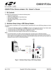
1
Si4010-DK
Si4010 D EVELOPMENT K I T U SER ’ S G UIDE
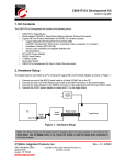
1. Key Fob Development Platform
The Si4010 key fob development platform is a flexible platform for comfortably developing software and testing the
whole system using the Silicon Laboratories software development IDE. The platform also allows programming of
the NVM on chip. The kit has three versions: one for the 434 MHz band (P/N 4010-KFOBDEV-434), one for the
868 MHz band (P/N 4010- KFOBDEV-868) and one for the 915 MHz band (P/N 4010-KFOBDEV-915).
1.1. Kit Content
Table 1. Kit Content
Qty
Part Number
Description
4010-KFOBDEV-434
Si4010 Key Fob Development Kit 434 MHz
2
4010-KFOB-434-NF
Si4010 key fob demo board 434 MHz w/o IC
1
MSC-DKPE1
3
Si4010-C2-GS
1
4010-DKPB434-BM
Si4010 MSOP key fob development board 434 MHz, SMA
1
4355-LED-434-SRX
Si4355 RFStick 434 MHz receiver board
1
MSC-PLPB_1
Key Fob Plastic Case (translucent grey)
1
MSC-BA5
Programming interface board
1
MSC-BA4
Burning adapter board
1
EC3
1
Toolstick_BA
Toolstick Base Adapter
1
MSC-DKCS5
USB Cable
SOIC/MSOP socketed development board
Si4010-C2-GS transmitter IC, SOIC Package
USB Debug Adapter
1
USB extender cable (USBA-USBA)
2
AAA
2
CRD2032
AAA battery
CR2032 3 V coin battery
4010-KFOBDEV-868
Si4010 Key Fob Development Kit 868 MHz
2
4010-KFOB-868-NF
1
MSC-DKPE1
3
Si4010-C2-GS
1
4010-DKPB868-BM
Si4010 MSOP key fob development board 868 MHz, SMA
1
4355-LED-868-SRX
Si4355 RFStick 868 MHz receiver board
Rev. 0.1 6/12
Si4010 key fob demo board 868 MHz w/o IC
SOIC/MSOP socketed development board
Si4010-C2-GS transmitter IC, SOIC Package
Copyright © 2012 by Silicon Laboratories
Si4010-DK
Si4010-DK
Table 1. Kit Content (Continued)
1
MSC-PLPB_1
1
MSC-BA5
Programming interface board
1
MSC-BA4
Burning adapter board
1
EC3
1
Toolstick_BA
Toolstick Base Adapter
1
MSC-DKCS5
USB Cable
1
USB Debug Adapter
USB extender cable (USBA-USBA)
2
AAA
2
CRD2032
4010-KFOBDEV-915
AAA battery
CR2032 3 V coin battery
Si4010 Key Fob Development Kit 915 MHz
2
4010-KFOB-915-NF
1
MSC-DKPE1
3
Si4010-C2-GS
1
4010-DKPB915-BM
Si4010 MSOP key fob development board 915 MHz, SMA
1
4355-LED-915-SRX
Si4355 RFStick 915MHz receiver board
1
MSC-PLPB_1
Key Fob Plastic Case (translucent grey)
1
MSC-BA5
Programming interface board
1
MSC-BA4
Burning adapter board
1
EC3
1
Toolstick_BA
Toolstick Base Adapter
1
MSC-DKCS5
USB Cable
1
2
Key Fob Plastic Case (translucent grey)
Si4010 key fob demo board 915 MHz w/o IC
SOIC/MSOP socketed development board
Si4010-C2-GS transmitter IC, SOIC Package
USB Debug Adapter
USB extender cable (USBA-USBA)
2
AAA
2
CRD2032
AAA battery
CR2032 3 V coin battery
Rev. 0.1
Si4010-DK
1.1.1. Burning Adapter (P/N MSC-BA4)
The programming interface board serves as an interface in between the debug adapter and the Socketed Key Fob
Development Board or the Development Key Fob. It provides 6.5 V for NVM programming. The power source is
activated by a sliding switch on the board. It is required when the user wants to program the internal NVM memory
on the chip.
The programming interface board contains an 8-pin header, to which GPIO0 to GPIO5, along with power and
ground, are connected from the development boards. Therefore, the user can tap to that header to control or
monitor the chip pins.
1.1.2. Si4010 Socketed Key Fob Development Board (P/N MSC-DKPE1)
Socketed (both SOIC and MSOP) key fob board with SMA connector.
Rev. 0.1
3
Si4010-DK
1.1.3. Si4010 MSOP Key Fob Development Board 434 MHz, SMA (P/N 4010-DKPB434-BM)
This development board has an unburned soldered Si4010, five push buttons, matched 50 SMA RF output,
battery clip, and battery switch. This board allows running user application from RAM during program development
even while board is disconnected and powered by the battery. The SMA output connector allows wired
measurements of the RF output signal.
Note: Instead of this board, some 434 MHz development kits may contain the pcb antenna version of this board, described in
"1.2.2. Si4010 Key Fob Development Board 434 MHz" on page 7.
1.1.4. Si4355 RFStick 434MHz receiver board (P/N 4355-LED-434-SRX)
Receiver board factory programmed with the simple receiver program srx_demo. Can be used for link testing with
Si4010 programmed with the rke_demo.
1.1.5. Programming Interface Board (P/N MSC-BA5)
Adapter board for interfacing customer PCB to the debug adapter.
4
Rev. 0.1
Si4010-DK
1.1.6. 4010 Key Fob Demo Board 434 MHz without IC (P/N 4010-KFOB-434-NF)
1.1.7. Key Fob Plastic Case (translucent grey) (P/N MSC-PLPB_1)
1.1.8. Toolstick Base Adapter (P/N Toolstick_BA)
Debugging adapter compatible with Si4355 RFstick receiver board and the Si4010 development boards.
1.1.9. Si4010 sample, SOIC package (P/N Si4010-C2-GS)
1.1.10. USB Cable (P/N MSC-DKCS5)
Cable to connect EC3 Debug Adapter to PC.
Rev. 0.1
5
Si4010-DK
1.1.11. EC3 Debug Adapter (P/N EC3)
Silicon Labs debugging adapter, used by other Silicon Labs’ MCU products as well, compatible with the
development platform.
6
Rev. 0.1
Si4010-DK
1.2. Other Boards
The following boards are not part of the development kit but can be ordered separately from Silicon Labs.
Part Number
4010-DKPB434-BS
Description
Si4010 SOIC key fob development board 434 MHz, SMA
4010-DKPB_434
Si4010 key fob development board 434 MHz
4010-DKMX_434
Si4010 matrix keyboard development board 434 MHz
4010-KFOB-315-NF
Si4010 key fob demo board 315 MHz w/o IC
1.2.1. Si4010 SOIC Key Fob Development Board 434 MHz, SMA
This board is similar to the board described in “1.1.3. Si4010 MSOP Key Fob Development Board 434 MHz, SMA
(P/N 4010-DKPB434-BM)” but contains the SOIC package version of the Si4010.
1.2.2. Si4010 Key Fob Development Board 434 MHz
This is also a key fob development board, but with a pcb antenna instead of the SMA connector.
Rev. 0.1
7
Si4010-DK
1.3. Usage of the Key Fob Development Platform
The Silicon Labs IDE communicates with the USB Debug Adapter through the USB bus. The following debugging
scenarios are possible:
1. EC3 debug adapter Burning adapterSi4010 socketed key fob development board
This setup is suitable for downloading, running, and debugging the program in RAM or burning the program in the
NVM and running it. The antenna or measuring instrument can be connected through an SMA connector. Since
sockets on board allow use of unsoldered ICs, this is the ideal scenario for burning the NVM memory of Si4010.
2. EC3 debug adapter Burning adapter Si4010 MSOP key fob development board
This setup is suitable for downloading, running, and debugging the program in RAM. This board has a PCB
antenna and battery, so after downloading the program and starting the execution by disconnecting in the IDE, the
board can be physically disconnected from the programming interface and tested in mobile form. A switch is
provided on the board to connect/disconnect the battery. The Toolstick Base Adapter can be also used in the two
above scenarios as a debug adapter. It can be connected to the pcb edge connector of the burning adapter.
Note: Although burning is also possible with this setup, it is not practical since Si4010 is soldered on the key fob development
board.
8
Rev. 0.1
Si4010-DK
3. EC3 debug adapter Programming adapter User’s own application
In this setup, the user can incorporate the debugging capabilities into the final application using a cheap 4-pin
header connection.
2. Debugging an Application
To debug an application the user is provided with the Silicon Laboratories IDE (Integrated Development
Environment). The IDE has an integral help. This section is not a user manual for the IDE, but highlights the items
which are important when working with the IDE.
2.1. Installing the IDE and USB Debug Adapters
Download the Silicon Labs IDE (Integrated Dvelopment Environment) from the following URL:
http://www.silabs.com/products/mcu/Pages/SiliconLaboratoriesIDE.aspx and install it on your computer. The IDE
gets installed into its own directory. The main executable file is IDE.exe. The IDE works with the USB Debug
Adapter or the Toolstick Base Adapter, shown in the section above. When the IDE recognizes the Silicon Labs USB
debug adapters, it queries whether its internal firmware is compatible with the Si4010. If not, then it notifies the user
and requests permission to update the adapter's firmware. Silicon Labs also provides a program,
usb_debug_adapter_firmware_reset.exe, to clear the adapter's firmware manually before connection to
the IDE. The program resides in the same directory as the IDE main executable.
With the Si4010 debugging chain it is required that the manual adapter firmware clearing is done for each USB
adapter before using the key fob debugging chain. That operation needs to be done only once per USB Debug
Adapter. The IDE will then program the correct firmware into the adapter.
The reset firmware executable will scan USB ports and give the user a list of connected Silicon Labs USB
adapters. The USB Debug Adapter name starts with EC. Users can have more than one USB adapter connected
to the computer.
2.2. Keil toolchain integration
The project files in examples assume that the Keil toolchain is installed into: C:\Keil directory. The location of
the Keil toolchain can be easily changed in the Silabs IDE in the Project—Tool Chain Integration menu. An
evaluation version of the Keil toolchain can be downloaded from the Keil website at http://www.keil.com/. This free
version has a 2 kB code limitation and starts the code at the 0x0800 address. The Keil free evaluation version can
be unlocked to become a 4 kB version with no code placement limitation by following the directions given in
application note AN104 about Keil toolchain integration and license management. Unlock code can be found on
the WDS CDROM in the root folder in the Keil_license_number.txt file. Contact your Silicon Laboratories sales
representative or distributor for application assistance.
Rev. 0.1
9
Si4010-DK
2.3. IDE Features
The IDE allows the following:
1. Download the OMF-51 linker output format (Keil BL51 linker output, for example) and match the source
code lines with the compiled file. This allows source code debugging, including variable value viewing, setting breakpoints, single-stepping, etc. Note that the output of the Keil LX51 linker is not understood by the
IDE.
2. Download the IntelHEX file for the application. When using the IntelHEX file the source code debugging is
not available. The user can set a breakpoint for a specific code address by going through the
Debug Breakpoints (Alt+B) menu item. The user can also single-step through the disassembly of the
loaded code.
3. Setting at least 4 breakpoints with a possible maximum of 8. The actual number of breakpoints available is
determined by the IDE from the factory setting of the chip.
4. Single-stepping through the disassembly of the code. If the OMF file is loaded, the single-stepping is
matched with the source code.
5. Viewing and changing variables, SFR registers, XREG registers, and the contents of both DATA/IDATA
RAM and CODE/XDATA RAM on the fly during debugging. When the changes are made by the user in the
corresponding windows, the user must press the Refresh Values (Alt+R) button on the toolbar to update
the values in the device. Just changing values in the IDE will not automatically update them in the device.
2.4. IDE Debugging Session
The typical IDE debugging session consists of the following sequence:
1. Connect the IDE to the chip by hitting the Connect or invoking menu Debug Connect menu item.
2. Download the OMF file either by hitting the Download code (Alt+D) toolbar button or from the
Debug Download object code menu item. The latter also allows IntelHEX download, but without the
source code debugging capability.
3. After the code download, the device is automatically halted at address 0x0000 in CODE/XDATA RAM.
Then the user can set breakpoints, single-step, animate, etc.
4. The user can hit the Reset (Ctrl+R) toolbar button any time the device is halted (not running). The internal
digital system level reset is invoked and the device goes through the boot sequence. The previously
loaded code by the user into the CODE/XDATA RAM is preserved and the device is halted at the address
0x0000 of CODE/XDATA RAM.
5. When a bug is found, the user can download a new OMF file whenever the device is halted. There is no
need to disconnect the device from the debug chain or to hit reset. The download, item 2 above, will automatically reset the device after the OMF/IntelHEX new code download is finished. It is very important to
note that whenever the Disconnect toolbar button is hit or the Debug Disconnect menu item is
invoked, the debugging chain does the following:
• Enables the LED driver. During the debugging sessions the LED current driver is forcibly disabled.
• Clears all the breakpoints.
• Releases the device from halt and lets it run from the point when it was halted.
2.5. Important Note about Single-Stepping Over ROM Code
Single-stepping through the ROM code is disabled. Whenever the user encounters the call to the ROM API
functions he or she should use the Step Over (F10) toolbar button rather than the Step (F11) or Multiple Step
button.
Even though single-stepping through the ROM API function using the Step (F11) button works from the user’s
point of view, the CPU timing is modified and real-time performance is not guaranteed when using the Step (F11)
or Multiple Step buttons over the ROM API functions. Therefore, it is highly recommended to use the Step Over
(F10) toolbar button when stepping over the ROM API functions in IDE.
Single-stepping over the bMtp_Write() function using Step (F11) or Multiple Step buttons may yield
unpredictable results in the MTP (EEPROM) and is highly discouraged. One should use the Step Over (F10) tool,
run to cursor, or setting a breakpoint when debugging around the MTP write function.
10
Rev. 0.1
Si4010-DK
2.6. Device Version
1. The device ID information can be read through the IDE through Views Debug Windows Si4010
XREG Regs. The last item bREV_ID is the device revision. The user can also call the API function
bSys_GetRevId().
2. The trim version can be read by the Silicon Labs IDE as External Memory through Views Debug Windows -> External Memory at location 0x11D6. There is a macro bSys_TrimId_c defined in the headers
for use in customer code as well. The user needs to know the TrimId before writing any code, so the manual access to it is adequate. The trim version will rarely change and customers will be notified about the
change.The provided NVM burner program reads both the bREV_ID device revision and the trim version
bSys_TrimId in the [Device] tab after the burner is connected to the device.
2.7. Debugging Application which Drives LED
To maximize utilization of the package pins, the LED current driver output is shared with the debug chain clock
signal C2CLK. To share the functionality and be able to use the IDE for debugging there are some limitations to
note and rules to follow. The following figure shows the recommended connection of the USB 10-pin debug header
to the device in the user application.
Note: The LED must be isolated by the 470 resistor for the debug chain to work.
Rev. 0.1
11
Si4010-DK
Facts about using the LED with IDE chain:
1. The IDE chain can connect to the device only if the LED current driver is off and the LED is not lit.
2. Once the IDE chain is connected to the device it blocks the device LED driver. Therefore, the application
can be written in a normal fashion using LED as desired in the final application without worry of being disconnected from the debug chain. The only limitation is that the LED will not be lit from the application during the IDE debug session. The user will still observe LED activity, but that activity is related to the debug
chain communicating with the device, not the user application driving the LED.
3. Once the IDE chain is disconnected from the device (for example, by pressing the Disconnect button in
the IDE), the device is released from halt and at the same time the blocking of the LED driver is removed.
From that point on, the application behaves and runs as a regular application and the LED activity reflects
what the application desires to do with the LED.
4. If the user wants to reconnect the IDE to the device the only requirement is that the LED must not be lit by
the application and the C2 debug interface must be active, not being actively turned off by the application.
Therefore, if the device user software is stuck in an infinite loop and driving the LED constantly or the C2
interface was turned off by the application, the IDE chain will not be able to connect to the device. In such
a situation, the device power has to be cycled to invoke internal power on reset. (See item 1 above.)
Cycling the power to the part in this context means either physical removal of the power to the device or
calling the vSys_Shutdown() function from within the application, which achieves the same result.
2.8. Hardware Issue with Debugging LED Application
There is an issue with the LED turning on and off and the functionality of the GPI04. There is no issue when the
part is programmed as the Run part and runs the final application code. Therefore, the issue affects only the
application development. There are several possible software workarounds, depending on the approach the user
wants to take.
2.8.1. Application LED Control
The user can control the LED intensity and whether the LED is on or off. The LED intensity has 4 values, 0 to 3:
Off, 0.3 mA, 0.6 mA, and 1 mA current. The user can set the intensity any time, but the LED is not going to be
turned on until the GPIO_LED is set to 1. The GPIO_LED is an alias for the P0.5 bit.
After the reset the P0.5 bit is set to 1, so it is recommended that the user use GPIO_LED = 0 at the beginning of the
user application.
To turn the LED off at the very beginning of the user application:
/* Clear the GPIO_LED.. reset will set this bit! */
GPIO_LED = 0;
To turn the LED on and off inside the user application:
/* Set LED intensity .. acceptable values are 0 (off) or 1, 2, and 3 */
vSys_LedIntensity( 3 );
…
/* To turn the LED on at currently set intensity */
GPIO_LED = 1;
…
/* To turn the LED off, keep the intensity setting */
GPIO_LED = 0;
12
Rev. 0.1
Si4010-DK
The intensity setting can be changed any time, even when the GPIO_LED = 1.
This is basically how the LED control operates. This approach will work when the part status is finalized as the Run
device, since for that program level the C2 interface is turned off after the boot-by-boot routine.
However, when the code above is used for a device in the Factory or User programming state, then the GPIO4 will
stop working after the first LED blink. The LED must be seen to be turned on and off by the application (to blink) to
experience this problem.
2.8.2. Solution 1: Living with the Limitation
The simplest solution is to know about the issue and decide to live with it. After the first LED blink, the GPI04 will
not work. In this scenario, the user may decide to test the GPI04 only when the part is fully programmed as the Run
part.
2.8.3. Solution 2: Controlled Compilation
The user may use a #define C statement to define a LED "on" value. For button press debugging purposes when
the LED can be off the code is compiled with value set as 0, so the LED will never light up and the GPIO4 will
always function. For debugging the LED, and for final application compilation for the Run state of the device, the
user will compile the application with the LED "on" value set to 1.
For example:
#ifdef DEBUG
#define gLedOnValue_c
0
#else
#define gLedOnValue_c
1
#endif
/* Clear the GPIO_LED off after reset .. reset will set this bit! */
GPIO_LED = 0;
/* Set LED intensity .. acceptable values are 0 (off) or 1, 2, and 3 */
vSys_LedIntensity( 3 );
…
/* Turn the LED on at currently set intensity */
GPIO_LED = gLedOnValue_c;
…
/* Turn the LED off, keep the intensity setting */
GPIO_LED = 0;
One advantage of this solution is that the code size is identical in both cases, Debug or Run. Cycling the power to
the part in this context means either physical removal of the power to the device or calling the vSys_Shutdown()
function from within the application, which achieves the same result.
2.8.4. Solution 3: Dynamic C2 Disable (Recommended)
The GPI04 issue manifests itself when the LED is actually being turned on and off from the application. The LED
physically blinks and is not blocked from being lit up by an application being connected to the IDE debug chain, and
the C2 interface is active and enabled.
Rev. 0.1
13
Si4010-DK
If we disable the C2 interface when the device is not connected to the IDE chain, and before the LED is turned off
when lit, then there will not be the GPIO4 problem. To do that the user must add the following function to the user
application to turn the LED on.
C function to turn the LED on:
/*
*-----------------------------------------------------------------------------*
*
INCLUDES:
*/
#include "si4010.h"
/*
*==============================================================================
*
*
VISIBLE FUNCTIONS:
*/
void
vLedOn
(
void
)
/*------------------------------------------------------------*
*
FUNCTION DESCRIPTION:
*
Turn LED on with disabling of the C2.
*
The C2 is disabled only if the part is not connected
*
to the IDE debugging chain.
*
*------------------------------------------------------------*/
{
/*
*------------------------------------------------------------*
VARIABLES:
*------------------------------------------------------------*/
GPIO_LED = 1;
if ( 0 != (RBIT_DATA & M_GPIO_LED_DRIVE) )
{
PROT0_CTRL |= M_C2_OFF;
}
}
14
Rev. 0.1
Si4010-DK
/*
*-----------------------------------------------------------------------------*/
Assembly version of the same function, assuming that the file name is ledon.a51 for
Keil toolchain.
;-----------------------------------------------------------------------------;
;
INCLUDES:
;
$NOLIST
$INCLUDE (si4010.inc)
$LIST
;--------------------------------------------------------------------------;
;
SEGMENTS:
;
; Assumes file name to be ledon.a51 .. capitalized LEDON is the file name
NAME
LEDON
?PR?vLedOn?LEDON SEGMENT CODE
;--------------------------------------------------------------------------;
;
EXTERNALS AND PUBLIC:
;
PUBLIC
vLedOn
;--------------------------------------------------------------------------;
;
CODE:
;
RSEG
?PR?vLedOn?LEDON
vLedOn:
setb
GPIO_LED
mov
A, RBIT_DATA
jnb
ACC.B_GPIO_LED_DRIVE, NoC2Disable
orl
PROT0_CTRL, #M_C2_OFF
NoC2Disable:
Rev. 0.1
15
Si4010-DK
ret
; -- End of assembly
END
;
;--------------------------------------------------------------------------;
The function is able to determine whether the device is connected to the IDE chain.
If it is not connected, then the function turns the C2 interface off. Once that is
done it is not possible to turn the C2 interface back on unless the power to the
device, or at least to the digital portion of the device, is cycled. See the
discussion below about advantages and disadvantages.
The following is an example of how to use the vLedOn() function:
/* Clear the GPIO_LED off after reset .. reset will set this bit! */
GPIO_LED = 0;
/* Set LED intensity .. acceptable values are 0 (off) or 1, 2, and 3 */
vSys_LedIntensity( 3 );
…
/* Turn the LED on at currently set intensity */
vLedOn();
…
/* Turn the LED off, keep the intensity setting */
GPIO_LED = 0;
Following are the advantages and disadvantages of this solution:
Advantages:
1. Uniform code, no need for conditional compilation, the GPIO4 and LED will function as expected under all
scenarios.
2. The user can use the GPIO_LED=1 in the code, which will block the GPIO4. But subsequent call to
vLedOn() will clear the blocking of the GPIO4 and it will start functioning normally again.
Disadvantages:
1. Once the LED is physically blinked then it is not possible for the IDE to connect to the part until the power is
cycled or the vSys_Shutdown() is called from within the application. It is up to the user to make sure that the
power is cycled.
2. If the part is programmed as the User part with the option to execute the user code after the boot automatically
without stopping, then the user application must not use the vLedOn() function just to blink LED without a user
input. If the application blinks the LED on its own, then the IDE will not be able to connect to the part, since the
C2 interface is disabled at the time when the LED is turned on. If the user does not use the option to execute
user code without stopping after the boot, there is not a problem since the device will load User code after the
reset and wait for further instructions, essentially waiting for the IDE to connect to it without executing the User
code.
16
Rev. 0.1
Si4010-DK
3. The vLedOn() function code is bigger than simple GPIO_LED=1 and is not necessary for the Run part, so
conditional compilation for LED bug may still be an option.
One recommendation for using the vLedOn() function is that the user application would include monitoring of
several buttons pressed simultaneously. If that combination happens, then the vSys_Shutdown() is invoked and
the IDE chain would be able to connect to the part again. That would satisfy the power cycling requirement without
actually cycling the physical power to the device.
2.9. Notes about USB Adapter Use
The following facts are worth noting when using the IDE debug chain:
1. Whenever the Reset button is pressed on the IDE, the system reset is invoked and the part goes through
a boot sequence.
2. Every time the new code, in OMF or HEX format, is downloaded to the part through the IDE, the IDE
issues a system reset and the device reboots. The content of the RAM memories is not touched by the
boot, with the exception of the API reserved regions in CODE/XDATA and DATA/IDATA memories. The
register banks RB0, RB1, and RB3 are cleared by the boot routine.
3. Whenever the ToolStick adapter is directly connected to the key fob design platform and the IDE is connecting to the part, the GPIO0 will be forcibly driven to 1 for about 260 ms around the beginning of the connection sequence. In the Silicon Labs-provided key fob platform, the GPIO0 isolated by a resistor, then if
the user is pressing a GPIO0 button during the connection sequence, the GPIO0 value will be viewed as 1
by the internal CPU during the IDE connection to the device.
4. It is recommended that the user uses the Burning adapter board along with the USB Debug Adapter.
Rev. 0.1
17
Si4010-DK
3. Examples provided
There are 5 demonstration examples provided with the development kit documentation pack:
1. aes_demo
2. fcast_demo
3. fstep_demo
4. tone_demo
5. keyfob_demo
6. rke_demo
All are precompiled and ready to be used without compilation for convenience. The user just needs to go to the
<name>_demo/bin directory and open the Silicon Labs IDE *.wsp project file by the Silicon Labs IDE.
Each demo can be built and debugged from within the Silicon Labs IDE.
3.1. AES demo-aes_demo
AES example with timer usage example. The timer counts the number of system clock cycles needed to run
encryption, decryption key preparation, and decryption.
3.2. Frequency casting demo-fcast_demo
This example shows the main flow when using the main vFCast_Tune tuning function. It also shows how to
transmit a predefined data packet when a button is pressed. The buttons are not debounced in this simple
example.
3.3. Frequency casting two step demo-fstep_demo
This example shows the main flow when the user wants to switch in between several frequencies fast. It is possible
to call vFCast_Tune()for several frequencies in advance, collect the information calculated, and then just quickly
apply it during transmission. This is for the cases when the 5-6 ms time spent in vFCast_Tune() is prohibitive for
switching in between frequencies.
3.4. Tone (CW) generation demo-tone_demo
This example shows the steps to generate continuous wave (tone) at a desired frequency. There are two main files
compiled to two separate example applications:
tone_demo
Run main tune vFCast_Tune once, then use only fine tuning to track the temperature changes.
tone_demo_ptune
Periodic tuning, run main tune vFCast_Tune every minute and use the fine tuning only in between the main tuning
events. However, there will be about 6 ms interruption of the output during the main tuning, once per minute.
The Keil µVision project tone_demo.Uv2 covers both targets:
tone_demo
tone_demo_ptune
For the Silicon Labs IDE there is only one target per *.wsp file, so there
are two project files:
tone_demo.wsp
tone_demo_ptune.wsp
18
Rev. 0.1
Si4010-DK
3.5. Simple key fob demo-keyfob_demo
This example demonstrates a basic key fob application transmitting a packet for every button push. Packets can be
received by an 4355-LED-XXX-SRX board. Buttons are debounced using the Button Service API functions.
3.6. RKE key fob demo-rke_demo
An advanced key fob demo using AES encryption, rolling counter in MTP memory, battery voltage measurement,
and production ID of chip as node address. This is the firmware used in the Si4010 Demo Key Fobs, available in
Silicon Labs key fob demo kits.
Rev. 0.1
19
Si4010-DK
CONTACT INFORMATION
Silicon Laboratories Inc.
400 West Cesar Chavez
Austin, TX 78701
Tel: 1+(512) 416-8500
Fax: 1+(512) 416-9669
Toll Free: 1+(877) 444-3032
Please visit the Silicon Labs Technical Support web page:
https://www.silabs.com/support/pages/contacttechnicalsupport.aspx
and register to submit a technical support request.
The information in this document is believed to be accurate in all respects at the time of publication but is subject to change without notice.
Silicon Laboratories assumes no responsibility for errors and omissions, and disclaims responsibility for any consequences resulting from
the use of information included herein. Additionally, Silicon Laboratories assumes no responsibility for the functioning of undescribed features
or parameters. Silicon Laboratories reserves the right to make changes without further notice. Silicon Laboratories makes no warranty, representation or guarantee regarding the suitability of its products for any particular purpose, nor does Silicon Laboratories assume any liability
arising out of the application or use of any product or circuit, and specifically disclaims any and all liability, including without limitation consequential or incidental damages. Silicon Laboratories products are not designed, intended, or authorized for use in applications intended to
support or sustain life, or for any other application in which the failure of the Silicon Laboratories product could create a situation where personal injury or death may occur. Should Buyer purchase or use Silicon Laboratories products for any such unintended or unauthorized application, Buyer shall indemnify and hold Silicon Laboratories harmless against all claims and damages.
Silicon Laboratories and Silicon Labs are trademarks of Silicon Laboratories Inc. Other products or brandnames mentioned herein are
trademarks or registered trademarks of their respective holders.
20
Rev. 0.1