1
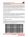
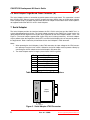
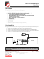
C8051F31X Development Kit
User’s Guide
1. Kit Contents
The C8051F31x Development Kit contains the following items:
•
•
•
•
•
•
•
•
C8051F31x Target Board
Serial Adapter (RS232 to Target Board Debug Interface Protocol Converter)
Cygnal IDE and Product Information CD-ROM. CD content includes:
• Cygnal Integrated Development Environment (IDE)
• Keil 8051 Development Tools (macro assembler, linker, evaluation ‘C’ compiler)
• Installation Untility (SETUP.EXE)
• Source code examples and register definition file
• Documentation
AC to DC Power Adapter
RS232 Serial Cable
7” Ribbon Cable
Quick-start Guide
C8051F31x Development Kit User’s Guide (this document)
2. Hardware Setup
The target board is connected to a PC running the Cygnal IDE via the Serial Adapter as shown in Figure 1.
1.
2.
3.
4.
Connect one end of the RS232 serial cable to a Serial (COM) Port on the PC.
Connect the other end of the RS232 serial cable to the DB-9 connector on the Serial Adapter.
Connect the Serial Adapter to the DEBUG connector on the target board with the10-pin ribbon cable.
Connect the AC/DC power adapter to power jack P1 on the target board.
AC/DC
Adapter
PC
Serial
Cable
Serial
Adpater
Ribbon Cable
Target Board
Serial Port
Figure 1. Hardware Setup
Note: The Reset switch on the target board is disabled when the serial adapter is connected to the
target board. Use the Reset button in the Cygnal IDE toolbar to reset the target when connected to
the Serial Adapter.
CYGNAL Integrated Products, Inc.
4301 Westbank Drive
Suite B-100
Austin, TX 78746
www.cygnal.com
Rev - 0.1 JUN02
Copyright © 2002 Cygnal Integrated Products, Inc.
(All rights reserved)
C8015F31X Development Kit User’s Guide
3. Software Setup
The included CD-ROM contains the Cygnal Integrated Development Environment (IDE), Keil software
8051 tools and additional documentation. Insert the CD-ROM into your PC’s CD-ROM drive. An installer
will automatically launch, allowing you to install the IDE software or read documentation by clicking buttons
on the Installation Panel. If the installer does not automatically start when you insert the CD-ROM, run
“autorun.exe” found in the root directory of the CD-ROM. Refer to the “readme.txt” file on the CD-ROM for
the latest information regarding known IDE problems and restrictions.
4. CYGNAL Integrated Development Environment
The Cygnal IDE integrates a source-code editor, source-level debugger and in-system Flash programmer.
The use of third-party compilers and assemblers is also supported. This development kit includes the Keil
Software A51 macro assembler, BL51 linker and evaluation version C51 ‘C’ compiler. These tools can be
used from within the Cygnal IDE.
4.1. System Requirements
The Cygnal IDE requirements:
•
•
•
Pentium-class host PC running Microsoft Windows 95 or later, or Microsoft Windows NT or later.
One available COM port (1-4).
64 MB RAM and 40MB free HD space recommended.
4.2. Assembler and Linker
A full-version Keil A51 macro assembler and BL51 banking linker are included with the development kit
and are installed during IDE installation. The complete assembler and linker reference manual can be
found on-line under the Help menu in the IDE or in the “Cygnal/hlp” directory (A51.pdf).
4.3. Evaluation C51 ‘C’ Compiler
An evaluation version of the Keil C51 ‘C’ compiler is included with the development kit and is installed during IDE installation . The evaluation version of the C51 compiler is the same as the full professional version
except code size is limited to 4K bytes and the floating point library is not included. The C51 compiler reference manual can be found under the Help menu in the IDE or in the “Cygnal/hlp” directory (C51.pdf).
4.4. Using the Keil Software 8051 Tools with the Cygnal IDE
To perform source-level debugging with the IDE, you must configure the Keil 8051 tools to generate an
absolute object file in the OMF-51 format with object extensions and debug records enabled. You may
build the OMF-51 absolute object file by calling the Keil 8051 tools at the command line (e.g. batch file or
make file) or by using the project manager built into the IDE. The default configuration when using the
Cygnal IDE project manger enables object extension and debug record generation. Refer to Applications
Note AN004 - Integrating Keil 8051 Tools Into the Cygnal IDE in the “Documentation” directory on the
CD-ROM for additional information on using the Keil 8051 tools with the Cygnal IDE.
To build an absolute object file using the Cygnal IDE project manager, you must first create a project. A project
consists of a set of files, IDE configuration, debug views, and a target build configuration (list of files and tool
configurations used as input to the assembler, compiler, and linker when building an output object file).
2
Rev - 0.1 JUN02
© 2002 Cygnal Integrated Products, Inc.
C8051F31X Development Kit User’s Guide
The following sections illustrate the steps necessary to manually create a project with one or more source
files, build a program and download the program to the target in preparation for debugging. (The IDE will
automatically create a single-file project using the currently open and active source file if you select Build/
Make Project before a project is defined.)
4.4.1. Creating a New Project
1. Select Project->New Project to open a new project and reset all configuration settings to default.
2. Select File->New File to open an editor window. Create your source file(s) and save the file(s) with
a recognized extension, such as .c, .h, or .asm, to enable color syntax highlighting.
3. Right-click on “New Project” in the Project Window. Select Add files to project. Select files in the
file browser and click Open. Continue adding files until all project files have been added.
4. For each of the files in the Project Window that you want assembled, compiled and linked into the
target build, right-click on the file name and select Add file to build. Each file will be assembled or
compiled as appropriate (based on file extension) and linked into the build of the absolute object file.
Note: If a project contains a large number of files, the “Group” feature of the IDE can be used to
organize. Right-click on “New Project” in the Project Window. Select Add Groups to project. Add
pre-defined groups or add customized groups. Right-click on the group name and choose Add file
to group. Select files to be added. Continue adding files until all project files have been added.
4.4.2. Building and Downloading the Program for Debugging
1. Once all source files have been added to the target build, build the project by clicking on the Build/
Make Project button in the toolbar or selecting Project->Build/Make Project from the menu.
2. C8051F31x family devices use the Cygnal 2-wire (C2) debug interface. You must select Cygnal
2-Wire in the Options->Debug Interface menu to enable connection to C8051F31x target devices.
Click the Connect button in the toolbar or select Debug->Connect from the menu to connect to the
device.
3. Download the project to the target by clicking the Download Code button in the toolbar.
Note: To enable automatic downloading if the program build is successful select Enable automatic connect/download after build in the Project->Target Build Configuration dialog. If
errors occur during the build process, the IDE will not attempt the download.
4. Save the project when finished with the debug session to preserve the current target build configuration, editor settings and the location of all open debug views. To save the project, select
Project->Save Project As... from the menu. Create a new name for the project and click on Save.
5. Example Source Code
Example source code and register definition files are provided in the “Examples/C8051F31x” directory during IDE installation. These files may be used as a template for code development. Example applications
include a blinking LED example which configures the green LED on the target to blink at a fixed rate.
© 2002 Cygnal Integrated Products, Inc.
Rev - 0.1 JUN02
3
C8015F31X Development Kit User’s Guide
5.1. Register Definition Files
Register definition files C8051F310.inc and C8051F310.h define all SFR registers and bit-addressable
control/status bits. They are installed into the “Examples/C8051F31x” directory during IDE installation. The
register and bit names are identical to those used in the C8051F31x datasheet. Both register definition files
are also installed in the default search path used by the Keil Software 8051 tools. Therefore, when using
the Keil 8051 tools included with the development kit (A51, C51), it is not necessary to copy a register
definition file to each project’s file directory.
5.2. Blinking LED Example
The example source files blink.asm and blinky.c show examples of several basic C8051F31x functions.
These include; disabling the watchdog timer (WDT), configuring the Port I/O crossbar, configuring a timer
for an interrupt routine, intializing the system clock, and configuring a GPIO port. When compiled/assembled and linked this program flashes the green LED on the C8051F31x target board about five times a second using the interrupt handler with a C8051F31x timer.
4
Rev - 0.1 JUN02
© 2002 Cygnal Integrated Products, Inc.
C8051F31X Development Kit User’s Guide
6. Target Board
The C8051F31x Development Kit includes a target board with a C8051F31x device pre-installed for evaluation and preliminary software development. Numerous inupt/output (I/O) connections are provided to facilitate prototyping using the target board. Refer to Figure 2 for the locations of the various I/O connectors.
P1
J1
J3
J5
J6
J7
J8
J9, J10
DEBUG
Power connector (accepts input from 7 to 15 VDC unregulated power adapter)
34-pin Expansion I/O connector
Port I/O Configuration Jumper Block
DB-9 connector for UART0 RS232 interface
Analog I/O terminal block
Low pass filter connector
Serial Adapter target board power connector
External crystal enable connectors
Used to connect the Serial Adapter to the target board via a 10-pin ribbon cable
RESET P0.7
Pin 1
Pin 2
J5
J3
J1
Pin 2
Pin 1
J9
C8051
F31X
DEBUG
Prototype Area
P3.3
J10
Pin 1
J7
J8
P1
J6
PWR
Pin 1
Prototyping Area I/O Connection Points
Figure 2. C8051F31x Target Board
© 2002 Cygnal Integrated Products, Inc.
Rev - 0.1 JUN02
5
C8015F31X Development Kit User’s Guide
6.1. System Clock Sources
The C8051F31x device installed on the target board features a calibrated programmable internal oscillator
which is enabled as the system clock source on reset. After reset, the internal oscillator operates at a frequency of 3.0625MHz (+/-2%) by default but may be configured by software to operate at other frequencies.
Therefore, in many applications an external oscillator is not required. However, if you wish to operate the
C8051F31x device at a frequency not available with the internal oscillator, an external crystal may be used.
Refer to the C8051F31x datasheet for more information on configuring the system clock source.
The target board is designed to facilitate the installation of an external crystal. Remove jumpers J9 and J10
and install the crystal at the pads marked Y1. Install a 10MΩ resistor at R9 and install capacitors at C14
and C15 using values appropriate for the crystal you select. Refer to the C8051F31x datasheet for more
information on the use of external oscillators.
6.2. Switches and LEDs
Two switches and two LEDs are provided on the target board. Switch SW1 is connected to the RESET pin
of the C8051F31x. Pressing SW1 puts the C8051F31x in its hardware-reset state.Switch SW2 is connected to the C8051F31x’s Port 0.7 (P0.7) general purpose I/O (GPIO) pin through jumper J3[3-4]. Pressing SW2 generates a logic low signal on the P0.7 pin. The P0.7 signal is also routed to a pin on the J1 I/O
connector. Remove the shorting block from J3[3-4] to disconnect SW2 from P0.7.
The LED labeled PWR is used to indicate a power connection to the target board. The LED labeled P3.3 is
connected to the C8051F31x’s Port 3.3 (P3.3) GPIO pin through jumper J3[1-2]. The P3.3 signal is also
routed to a pin on the J1 I/O connector. Remove the shorting block from J3[1-2] to disconnect the LED
from P3.3.
6.3. Expansion I/O Connector (J1)
The 34-pin Expansion I/O connector J1 provides access to all signal pins of the C8051F31x device. Pins
for +3V, digital ground and the output of an on-board low-pass filter are also available. A small throughhole prototyping area is also provided. All I/O signals routed to connector J1 are also routed to throughhole connection points between J1 and the prototyping area (see Figure 2 on page 5). Each connection
point is labeled indicating the signal available at the connection point.
Pin #
Description
Pin #
Description
Pin #
Description
1
2
3
4
5
6
7
8
9
10
11
12
+3VD (+3.3VDC)
PWM Output
P0.0
P0.1
P0.2
P0.3
P0.4
P0.5
P0.6
P0.7
P1.0
P1.1
13
14
15
16
17
18
19
20
21
22
23
24
P1.2
P1.3
P1.4
P1.5
P1.6
P1.7
P2.0
P2.1
P2.2
P2.3
P2.4
P2.5
25
26
27
28
29
30
31
32
33
34
P2.6
P2.7
P3.0
P3.1
P3.2
P3.3
P3.4
/RST (Reset)
GND (Ground)
GND (Ground)
Table 1. J1 Pin Descriptions
6
Rev - 0.1 JUN02
© 2002 Cygnal Integrated Products, Inc.
C8051F31X Development Kit User’s Guide
6.4. Target Board DEBUG Interface (J4)
The DEBUG connector (J4) provides access to the DEBUG pins of the C8051F31x. It is used to connect
the Serial Adapter to the target board for in-circuit debugging and Flash programming. Table 2 shows the
J4 pin definitions.
Pin #
Description
1
2, 3, 9
4
5
6
7
8
10
+3VD (+3.3VDC)
GND (Ground)
C2DAT
/RST (Reset)
P3.0
C2CK
Not Connected
J4_Pin_10
Table 2. DEBUG Connector Pin Descriptions
6.5. Serial Interface (J5)
A RS232 transceiver circuit and DB-9 (J5) connector are provided on the target board to facilitate serial
connections to UART0 of the C8051F31x. The TX and RX signals of UART0 may be connected to the
DB-9 connector and transceiver by installing jumpers on J3.
J3[5-6] - Install shorting block to connect UART0 TX (P0.4) to transceiver.
J3[7-8] - Install shorting block to connect UART0 RX (P0.5) to transceiver.
6.6. Analog I/O (J6)
Several of the C8051F31x target device’s port pins are connected to the J6 terminal block. Refer to Table 3
for the J6 terminal block connections. Install a shorting block on J7[2-3] to connect the AIN2.4 input to the
P2.4 pin of the target device.
Pin #
Description
1
2
3
4
P2.5 / AIN2.5
AIN2.4
GND (Ground)
P0.0 / Vref (Voltage Reference)
Table 3. J6 Terminal Block Pin Descriptions
6.7. Low-pass Filter (J7)
The target board features a low-pass filter that may be connected to port pin P2.4. Install a shorting block
on J7[1-2] to connect the P2.4 pin of the target device to the low-pass filter input. The output of the lowpass filter is routed to the PWM signal at J1[2]. The C8051F31x may be programmed to generate a PWM
(Pulse-Width Modulated) waveform which is then input to the low-pass filter to implement a user-controlled
PWM digital-to-analog converter. Refer to Applications Note AN007 - Implementing 16-Bit PWM Using
the PCA in the “documentation” directory on the CD-ROM for a discussion on generating a programmable
DC voltage level with a PWM waveform and low-pass filter.
© 2002 Cygnal Integrated Products, Inc.
Rev - 0.1 JUN02
7
C8015F31X Development Kit User’s Guide
6.8. Serial Adapter Target Board Power Connector (J8)
The Serial Adapter includes a connection to provide power to the target board. This connection is routed
from J4[10] to J8[1]. Place a jumper at J8[2-3] to power the board directly from an AC/DC power adapter.
Place a jumper at J8[1-2] to power the board from the Serial Adapter. Please note that the second option is
not supported with either the EC1 or EC2 Serial Adapters.
7. Serial Adapter
The Serial Adapter provides the interface between the PC’s RS232 serial port and the C8051F31x’s insystem debug/programming circuitry. The Serial Adapter connects to the C8051F31x Cygnal 2-wire (C2)
debug interface on the target board using the 10-pin connector on the Serial Adapter labeled “JTAG”, see
Figure 3. (The Serial Adapter supports both Cygnal JTAG and C2 debug interfaces.). All Serial Adapters
may be powered from the target board, but the EC1 and EC2 Serial Adapter units can not provide power to
the target board. Table 4 shows the pin definitions for the Serial Adapter’s JTAG connector.
Notes:
1. When powering the Serial Adapter via the JTAG connector, the input voltage to the JTAG connector’s power pin must be 3.0 to 3.6VDC. Otherwise, the Serial Adapter must be powered directly by
connecting the AC/DC adapter to the Serial Adapter’s DC power jack.
2. The Serial Adapter requires a target system clock of 32Khz or greater.
Pin #
Description
1
2
4
5
6
7
3,8,9,10
3.0 to 3.6VDC Input
GND (Ground)
TCK (C2DAT)
TMS
TDO
TDI (C2CLK)
Not Connected
JTAG
Serial
Adapter
RS232
Pwr
Run/
Stop
Table 4. DEBUG Connector Pin Descriptions
Pin 1
Pin 2
Figure 3. Serial Adapter JTAG Connector
8
Rev - 0.1 JUN02
© 2002 Cygnal Integrated Products, Inc.
C8051F31X Development Kit User’s Guide
Figure 4. C8051F31x Target Board Schematic
8. Schematic
© 2002 Cygnal Integrated Products, Inc.
Rev - 0.1 JUN02
9