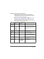
1
ACS800
Firmware Manual
IGBT Supply Control Program 7.x
ACS800 IGBT Supply Control Program 7.x
Firmware Manual
3AFE68315735 Rev E
EN
EFFECTIVE: 2011-10-07
© 2011 ABB Oy. All Rights Reserved.
5
Table of contents
Table of contents
Introduction to the manual
What this chapter contains . . . . . . . . . . . . . . . . . . . . . . . . . . . . . . . . . . . . . . . . . . . . . . . . . . . . . . . . 9
Compatibility . . . . . . . . . . . . . . . . . . . . . . . . . . . . . . . . . . . . . . . . . . . . . . . . . . . . . . . . . . . . . . . . . . . 9
Safety instructions . . . . . . . . . . . . . . . . . . . . . . . . . . . . . . . . . . . . . . . . . . . . . . . . . . . . . . . . . . . . . . . 9
Reader . . . . . . . . . . . . . . . . . . . . . . . . . . . . . . . . . . . . . . . . . . . . . . . . . . . . . . . . . . . . . . . . . . . . . . . . 9
Terms . . . . . . . . . . . . . . . . . . . . . . . . . . . . . . . . . . . . . . . . . . . . . . . . . . . . . . . . . . . . . . . . . . . . . . . . 9
Contents . . . . . . . . . . . . . . . . . . . . . . . . . . . . . . . . . . . . . . . . . . . . . . . . . . . . . . . . . . . . . . . . . . . . . 11
Start-up
What this chapter contains . . . . . . . . . . . . . . . . . . . . . . . . . . . . . . . . . . . . . . . . . . . . . . . . . . . . . . . 13
How to start-up the converter . . . . . . . . . . . . . . . . . . . . . . . . . . . . . . . . . . . . . . . . . . . . . . . . . . . . . 13
Program features
What this chapter contains . . . . . . . . . . . . . . . . . . . . . . . . . . . . . . . . . . . . . . . . . . . . . . . . . . . . . . .
Symbols used . . . . . . . . . . . . . . . . . . . . . . . . . . . . . . . . . . . . . . . . . . . . . . . . . . . . . . . . . . . . . . . . .
Local control vs. external control . . . . . . . . . . . . . . . . . . . . . . . . . . . . . . . . . . . . . . . . . . . . . . . . . . .
DriveWindow connection . . . . . . . . . . . . . . . . . . . . . . . . . . . . . . . . . . . . . . . . . . . . . . . . . . . . . .
Identification routine . . . . . . . . . . . . . . . . . . . . . . . . . . . . . . . . . . . . . . . . . . . . . . . . . . . . . . . . . . . .
Settings and diagnostics . . . . . . . . . . . . . . . . . . . . . . . . . . . . . . . . . . . . . . . . . . . . . . . . . . . . . . .
Charging . . . . . . . . . . . . . . . . . . . . . . . . . . . . . . . . . . . . . . . . . . . . . . . . . . . . . . . . . . . . . . . . . . . . .
Settings and diagnostics . . . . . . . . . . . . . . . . . . . . . . . . . . . . . . . . . . . . . . . . . . . . . . . . . . . . . . .
Synchronisation . . . . . . . . . . . . . . . . . . . . . . . . . . . . . . . . . . . . . . . . . . . . . . . . . . . . . . . . . . . . . . . .
Settings and diagnostics . . . . . . . . . . . . . . . . . . . . . . . . . . . . . . . . . . . . . . . . . . . . . . . . . . . . . . .
Starting sequence . . . . . . . . . . . . . . . . . . . . . . . . . . . . . . . . . . . . . . . . . . . . . . . . . . . . . . . . . . . . . .
Start by the operating switch (I/O control) . . . . . . . . . . . . . . . . . . . . . . . . . . . . . . . . . . . . . . . . .
Start in local control mode . . . . . . . . . . . . . . . . . . . . . . . . . . . . . . . . . . . . . . . . . . . . . . . . . . . . .
Start via fieldbus . . . . . . . . . . . . . . . . . . . . . . . . . . . . . . . . . . . . . . . . . . . . . . . . . . . . . . . . . . . . .
Settings and diagnostics . . . . . . . . . . . . . . . . . . . . . . . . . . . . . . . . . . . . . . . . . . . . . . . . . . . . . . .
Stop . . . . . . . . . . . . . . . . . . . . . . . . . . . . . . . . . . . . . . . . . . . . . . . . . . . . . . . . . . . . . . . . . . . . . . . . .
Missing phase . . . . . . . . . . . . . . . . . . . . . . . . . . . . . . . . . . . . . . . . . . . . . . . . . . . . . . . . . . . . . . . . .
Settings and diagnostics . . . . . . . . . . . . . . . . . . . . . . . . . . . . . . . . . . . . . . . . . . . . . . . . . . . . . . .
Control diagram . . . . . . . . . . . . . . . . . . . . . . . . . . . . . . . . . . . . . . . . . . . . . . . . . . . . . . . . . . . . . . . .
Controllers . . . . . . . . . . . . . . . . . . . . . . . . . . . . . . . . . . . . . . . . . . . . . . . . . . . . . . . . . . . . . . . . . . . .
DC voltage control . . . . . . . . . . . . . . . . . . . . . . . . . . . . . . . . . . . . . . . . . . . . . . . . . . . . . . . . . . . . . .
Settings and diagnostics . . . . . . . . . . . . . . . . . . . . . . . . . . . . . . . . . . . . . . . . . . . . . . . . . . . . . . .
Reactive power control . . . . . . . . . . . . . . . . . . . . . . . . . . . . . . . . . . . . . . . . . . . . . . . . . . . . . . . . . .
Settings and diagnostics . . . . . . . . . . . . . . . . . . . . . . . . . . . . . . . . . . . . . . . . . . . . . . . . . . . . . . .
Reduced Run Function . . . . . . . . . . . . . . . . . . . . . . . . . . . . . . . . . . . . . . . . . . . . . . . . . . . . . . . . . .
Removing a broken converter module . . . . . . . . . . . . . . . . . . . . . . . . . . . . . . . . . . . . . . . . . . . .
15
15
15
15
16
16
16
16
17
17
17
18
20
21
22
22
23
23
24
24
25
25
26
26
27
27
Table of contents
6
Settings and diagnostics . . . . . . . . . . . . . . . . . . . . . . . . . . . . . . . . . . . . . . . . . . . . . . . . . . . . . .
Inverter fan speed control . . . . . . . . . . . . . . . . . . . . . . . . . . . . . . . . . . . . . . . . . . . . . . . . . . . . . . . .
Settings . . . . . . . . . . . . . . . . . . . . . . . . . . . . . . . . . . . . . . . . . . . . . . . . . . . . . . . . . . . . . . . . . . .
RMIO board connection diagrams . . . . . . . . . . . . . . . . . . . . . . . . . . . . . . . . . . . . . . . . . . . . . . . . .
Temperature sensors . . . . . . . . . . . . . . . . . . . . . . . . . . . . . . . . . . . . . . . . . . . . . . . . . . . . . . . . . . .
Thermal sensor connection through I/O . . . . . . . . . . . . . . . . . . . . . . . . . . . . . . . . . . . . . . . . . .
Settings . . . . . . . . . . . . . . . . . . . . . . . . . . . . . . . . . . . . . . . . . . . . . . . . . . . . . . . . . . . . . . . . .
Diagnostics . . . . . . . . . . . . . . . . . . . . . . . . . . . . . . . . . . . . . . . . . . . . . . . . . . . . . . . . . . . . . .
Thermal connection through analogue I/O extension . . . . . . . . . . . . . . . . . . . . . . . . . . . . . . . .
Settings . . . . . . . . . . . . . . . . . . . . . . . . . . . . . . . . . . . . . . . . . . . . . . . . . . . . . . . . . . . . . . . . .
Diagnostics . . . . . . . . . . . . . . . . . . . . . . . . . . . . . . . . . . . . . . . . . . . . . . . . . . . . . . . . . . . . . .
28
29
29
30
32
33
33
33
34
34
35
Actual signals and parameters
What this chapter contains . . . . . . . . . . . . . . . . . . . . . . . . . . . . . . . . . . . . . . . . . . . . . . . . . . . . . . .
Fieldbus equivalent . . . . . . . . . . . . . . . . . . . . . . . . . . . . . . . . . . . . . . . . . . . . . . . . . . . . . . . . . . . .
Fieldbus addresses . . . . . . . . . . . . . . . . . . . . . . . . . . . . . . . . . . . . . . . . . . . . . . . . . . . . . . . . . . . .
Modbus and Modbus Plus address . . . . . . . . . . . . . . . . . . . . . . . . . . . . . . . . . . . . . . . . . . . . . .
Terms and abbreviations . . . . . . . . . . . . . . . . . . . . . . . . . . . . . . . . . . . . . . . . . . . . . . . . . . . . . . . .
01 ACTUAL SIGNALS . . . . . . . . . . . . . . . . . . . . . . . . . . . . . . . . . . . . . . . . . . . . . . . . . . . . . . . . . .
02 ACTUAL SIGNALS . . . . . . . . . . . . . . . . . . . . . . . . . . . . . . . . . . . . . . . . . . . . . . . . . . . . . . . . . .
03 ACTUAL SIGNALS . . . . . . . . . . . . . . . . . . . . . . . . . . . . . . . . . . . . . . . . . . . . . . . . . . . . . . . . . .
04 INFORMATION . . . . . . . . . . . . . . . . . . . . . . . . . . . . . . . . . . . . . . . . . . . . . . . . . . . . . . . . . . . . .
07 CONTROL WORDS . . . . . . . . . . . . . . . . . . . . . . . . . . . . . . . . . . . . . . . . . . . . . . . . . . . . . . . . .
08 STATUS WORDS . . . . . . . . . . . . . . . . . . . . . . . . . . . . . . . . . . . . . . . . . . . . . . . . . . . . . . . . . . .
09 FAULT WORDS . . . . . . . . . . . . . . . . . . . . . . . . . . . . . . . . . . . . . . . . . . . . . . . . . . . . . . . . . . . .
11 REFERENCE SELECT . . . . . . . . . . . . . . . . . . . . . . . . . . . . . . . . . . . . . . . . . . . . . . . . . . . . . . .
13 ANALOGUE INPUTS . . . . . . . . . . . . . . . . . . . . . . . . . . . . . . . . . . . . . . . . . . . . . . . . . . . . . . . .
14 DIGITAL OUTPUTS . . . . . . . . . . . . . . . . . . . . . . . . . . . . . . . . . . . . . . . . . . . . . . . . . . . . . . . . .
15 ANALOGUE OUTPUTS . . . . . . . . . . . . . . . . . . . . . . . . . . . . . . . . . . . . . . . . . . . . . . . . . . . . . .
16 SYSTEM CTR INPUTS . . . . . . . . . . . . . . . . . . . . . . . . . . . . . . . . . . . . . . . . . . . . . . . . . . . . . . .
18 LED PANEL CTRL . . . . . . . . . . . . . . . . . . . . . . . . . . . . . . . . . . . . . . . . . . . . . . . . . . . . . . . . . .
19 DATA STORAGE . . . . . . . . . . . . . . . . . . . . . . . . . . . . . . . . . . . . . . . . . . . . . . . . . . . . . . . . . . .
21 START/STOP . . . . . . . . . . . . . . . . . . . . . . . . . . . . . . . . . . . . . . . . . . . . . . . . . . . . . . . . . . . . . .
22 CACP PARALL CTRL . . . . . . . . . . . . . . . . . . . . . . . . . . . . . . . . . . . . . . . . . . . . . . . . . . . . . . . .
23 DC VOLT REF . . . . . . . . . . . . . . . . . . . . . . . . . . . . . . . . . . . . . . . . . . . . . . . . . . . . . . . . . . . . . .
24 REACTIVE POWER . . . . . . . . . . . . . . . . . . . . . . . . . . . . . . . . . . . . . . . . . . . . . . . . . . . . . . . . .
30 FAULT FUNCTIONS . . . . . . . . . . . . . . . . . . . . . . . . . . . . . . . . . . . . . . . . . . . . . . . . . . . . . . . . .
31 AUTOMATIC RESET . . . . . . . . . . . . . . . . . . . . . . . . . . . . . . . . . . . . . . . . . . . . . . . . . . . . . . . .
51 MASTER ADAPTER . . . . . . . . . . . . . . . . . . . . . . . . . . . . . . . . . . . . . . . . . . . . . . . . . . . . . . . . .
52 STANDARD MODBUS . . . . . . . . . . . . . . . . . . . . . . . . . . . . . . . . . . . . . . . . . . . . . . . . . . . . . . .
53 USER PARAMETERS . . . . . . . . . . . . . . . . . . . . . . . . . . . . . . . . . . . . . . . . . . . . . . . . . . . . . . . .
55 ADAPTIVE PROG1 . . . . . . . . . . . . . . . . . . . . . . . . . . . . . . . . . . . . . . . . . . . . . . . . . . . . . . . . . .
56 ADAPT PROG1 CNTRL . . . . . . . . . . . . . . . . . . . . . . . . . . . . . . . . . . . . . . . . . . . . . . . . . . . . . .
57 ADAPTIVE PROG2 . . . . . . . . . . . . . . . . . . . . . . . . . . . . . . . . . . . . . . . . . . . . . . . . . . . . . . . . . .
58 ADAPT PROG2 CNTRL . . . . . . . . . . . . . . . . . . . . . . . . . . . . . . . . . . . . . . . . . . . . . . . . . . . . . .
66 ADAPTIVE CONNECT . . . . . . . . . . . . . . . . . . . . . . . . . . . . . . . . . . . . . . . . . . . . . . . . . . . . . . .
70 DDCS CONTROL . . . . . . . . . . . . . . . . . . . . . . . . . . . . . . . . . . . . . . . . . . . . . . . . . . . . . . . . . . .
71 DRIVEBUS COM . . . . . . . . . . . . . . . . . . . . . . . . . . . . . . . . . . . . . . . . . . . . . . . . . . . . . . . . . . . .
90 DATA SET RECEIVE ADDRESSES . . . . . . . . . . . . . . . . . . . . . . . . . . . . . . . . . . . . . . . . . . . . .
Table of contents
37
37
37
37
37
38
39
39
40
40
40
40
42
42
43
44
45
47
48
48
49
50
51
53
57
58
58
58
59
60
61
63
64
64
66
66
7
91 DATA SET RECEIVE ADDRESSES . . . . . . . . . . . . . . . . . . . . . . . . . . . . . . . . . . . . . . . . . . . . .
92 DATA SET TRANSMIT ADDRESSES . . . . . . . . . . . . . . . . . . . . . . . . . . . . . . . . . . . . . . . . . . . .
93 DATA SET TRANSMIT ADDRESSES . . . . . . . . . . . . . . . . . . . . . . . . . . . . . . . . . . . . . . . . . . . .
98 OPTION MODULES . . . . . . . . . . . . . . . . . . . . . . . . . . . . . . . . . . . . . . . . . . . . . . . . . . . . . . . . . .
99 START UP DATA . . . . . . . . . . . . . . . . . . . . . . . . . . . . . . . . . . . . . . . . . . . . . . . . . . . . . . . . . . . .
67
67
69
69
71
Fieldbus control
What this chapter contains . . . . . . . . . . . . . . . . . . . . . . . . . . . . . . . . . . . . . . . . . . . . . . . . . . . . . . .
System overview . . . . . . . . . . . . . . . . . . . . . . . . . . . . . . . . . . . . . . . . . . . . . . . . . . . . . . . . . . . . . . .
Setting up communication through fieldbus . . . . . . . . . . . . . . . . . . . . . . . . . . . . . . . . . . . . . . . . . .
Setting up communication through the Standard Modbus Link . . . . . . . . . . . . . . . . . . . . . . . . . . . .
Setting up communication through Advant Controller . . . . . . . . . . . . . . . . . . . . . . . . . . . . . . . . . . .
Setting up communication through inverter module . . . . . . . . . . . . . . . . . . . . . . . . . . . . . . . . . . . .
Setting up communication through CACP . . . . . . . . . . . . . . . . . . . . . . . . . . . . . . . . . . . . . . . . . . . .
Setting up communication by CASCADE or INU COM WIDE . . . . . . . . . . . . . . . . . . . . . . . . . . . . .
Fieldbus control interface . . . . . . . . . . . . . . . . . . . . . . . . . . . . . . . . . . . . . . . . . . . . . . . . . . . . . . . .
Datasets 1 and 2 . . . . . . . . . . . . . . . . . . . . . . . . . . . . . . . . . . . . . . . . . . . . . . . . . . . . . . . . . . . .
Datasets 10...25 . . . . . . . . . . . . . . . . . . . . . . . . . . . . . . . . . . . . . . . . . . . . . . . . . . . . . . . . . . . . .
Received datasets . . . . . . . . . . . . . . . . . . . . . . . . . . . . . . . . . . . . . . . . . . . . . . . . . . . . . . . . .
Transmitted datasets . . . . . . . . . . . . . . . . . . . . . . . . . . . . . . . . . . . . . . . . . . . . . . . . . . . . . . .
Block diagram: reference select . . . . . . . . . . . . . . . . . . . . . . . . . . . . . . . . . . . . . . . . . . . . . . .
Data words . . . . . . . . . . . . . . . . . . . . . . . . . . . . . . . . . . . . . . . . . . . . . . . . . . . . . . . . . . . . . . . . . . .
07.01 MAIN CTRL WORD . . . . . . . . . . . . . . . . . . . . . . . . . . . . . . . . . . . . . . . . . . . . . . . . . . . . .
07.03 AUX CTRL WORD 2 . . . . . . . . . . . . . . . . . . . . . . . . . . . . . . . . . . . . . . . . . . . . . . . . . . . .
08.01 MAIN STATUS WORD . . . . . . . . . . . . . . . . . . . . . . . . . . . . . . . . . . . . . . . . . . . . . . . . . . .
08.05 DI STATUS WORD . . . . . . . . . . . . . . . . . . . . . . . . . . . . . . . . . . . . . . . . . . . . . . . . . . . . .
Fault and alarm words . . . . . . . . . . . . . . . . . . . . . . . . . . . . . . . . . . . . . . . . . . . . . . . . . . . . . . . . . . .
09.01 FAULT WORD 1 . . . . . . . . . . . . . . . . . . . . . . . . . . . . . . . . . . . . . . . . . . . . . . . . . . . . . . . .
09.02 FAULT WORD 2 . . . . . . . . . . . . . . . . . . . . . . . . . . . . . . . . . . . . . . . . . . . . . . . . . . . . . . . .
09.03 FAULT WORD 3 . . . . . . . . . . . . . . . . . . . . . . . . . . . . . . . . . . . . . . . . . . . . . . . . . . . . . . . .
09.04 ALARM WORD 1 . . . . . . . . . . . . . . . . . . . . . . . . . . . . . . . . . . . . . . . . . . . . . . . . . . . . . . .
09.11 SUPPLY FAULT WORD . . . . . . . . . . . . . . . . . . . . . . . . . . . . . . . . . . . . . . . . . . . . . . . . . .
09.12 SUPPLY ALARM WORD . . . . . . . . . . . . . . . . . . . . . . . . . . . . . . . . . . . . . . . . . . . . . . . . .
09.13 CURRENT UNBALANCE . . . . . . . . . . . . . . . . . . . . . . . . . . . . . . . . . . . . . . . . . . . . . . . . .
09.14 OVERCURRENT FAULT . . . . . . . . . . . . . . . . . . . . . . . . . . . . . . . . . . . . . . . . . . . . . . . . .
09.15 SHORT CIRC FAULT . . . . . . . . . . . . . . . . . . . . . . . . . . . . . . . . . . . . . . . . . . . . . . . . . . . .
09.16 OVERTEMP WORD . . . . . . . . . . . . . . . . . . . . . . . . . . . . . . . . . . . . . . . . . . . . . . . . . . . . .
09.17 TEMP DIF FLT WORD . . . . . . . . . . . . . . . . . . . . . . . . . . . . . . . . . . . . . . . . . . . . . . . . . . .
09.18 TEMP DIF ALM WORD . . . . . . . . . . . . . . . . . . . . . . . . . . . . . . . . . . . . . . . . . . . . . . . . . .
73
73
75
76
77
79
80
82
83
83
84
84
85
86
87
87
87
88
89
90
90
90
91
91
92
92
93
93
94
94
95
95
Fault tracing
What this chapter contains . . . . . . . . . . . . . . . . . . . . . . . . . . . . . . . . . . . . . . . . . . . . . . . . . . . . . . . 97
Safety . . . . . . . . . . . . . . . . . . . . . . . . . . . . . . . . . . . . . . . . . . . . . . . . . . . . . . . . . . . . . . . . . . . . . . . 97
Alarm and fault indications . . . . . . . . . . . . . . . . . . . . . . . . . . . . . . . . . . . . . . . . . . . . . . . . . . . . . . . 97
How to reset . . . . . . . . . . . . . . . . . . . . . . . . . . . . . . . . . . . . . . . . . . . . . . . . . . . . . . . . . . . . . . . . . . 97
Fault history . . . . . . . . . . . . . . . . . . . . . . . . . . . . . . . . . . . . . . . . . . . . . . . . . . . . . . . . . . . . . . . . . . . 97
Warning messages . . . . . . . . . . . . . . . . . . . . . . . . . . . . . . . . . . . . . . . . . . . . . . . . . . . . . . . . . . . . . 98
Fault messages . . . . . . . . . . . . . . . . . . . . . . . . . . . . . . . . . . . . . . . . . . . . . . . . . . . . . . . . . . . . . . . 101
Table of contents
8
Further information
Product and service inquiries . . . . . . . . . . . . . . . . . . . . . . . . . . . . . . . . . . . . . . . . . . . . . . . . . . . .
Product training . . . . . . . . . . . . . . . . . . . . . . . . . . . . . . . . . . . . . . . . . . . . . . . . . . . . . . . . . . . . . .
Providing feedback on ABB Drives manuals . . . . . . . . . . . . . . . . . . . . . . . . . . . . . . . . . . . . . . . .
Document library on the Internet . . . . . . . . . . . . . . . . . . . . . . . . . . . . . . . . . . . . . . . . . . . . . . . . .
Table of contents
107
107
107
107
9
Introduction to the manual
What this chapter contains
This chapter includes a description of the contents of the manual. In addition, it
contains information about the compatibility, safety and intended audience.
Compatibility
This manual is compatible with the following programs:
• version IXXR7270 IGBT supply control program. This program is used in the lineside converters of ACS800 multidrive, ACS800-17 and ACS800-11/U11.
• version ILXR7270 IGBT supply control program. This program is used in the lineside converters of ACS800-37, ACS800-37LC and ACS800-31/U31.
Safety instructions
Follow all safety instructions delivered with the drive.
• Read the complete safety instructions before you install, commission, or use
the drive. For single drives, the complete safety instructions are given at the
beginning of the hardware manual. For multidrive safety instructions, see
ACS800 Multidrive Safety Instructions (3AFE64760432 [English]).
• Read the software function specific warnings and notes before changing the
default settings of the function. For each function, the warnings and notes are
given in this manual in the subsection describing the related user-adjustable
parameters.
Reader
The reader of the manual is expected to know the standard electrical wiring
practices, electronic components and electrical schematic symbols.
Terms
Term
Description
Line-side converter /
converter
In this manual the ACS800 IGBT supply unit is referred to as
line-side converter / converter.
DriveWindow
PC tool for operating, controlling and monitoring ABB drives
APBU/NPBU
Branching unit for parallel connected converters
INT
Main Circuit Interface Board
RDCO
DDCS Communication Option module
Introduction to the manual
10
RDCU
Drive Control Unit
RMIO
Motor Control and I/O Board
Introduction to the manual
11
Contents
The manual consists of the following chapters:
• Start-up contains the basic start-up procedure of the line-side converter.
• Program features contains the feature descriptions and the reference lists of the
user settings and diagnostic signals.
• Actual signals and parameters describes the actual signals and parameters of the
line-side converter.
• Fieldbus control describes the communication through serial communication
links.
• Fault tracing lists the warning and fault messages with the possible causes and
remedies.
Introduction to the manual
12
Introduction to the manual
13
Start-up
What this chapter contains
This chapter contains the basic start-up procedure of the line-side converter.
How to start-up the converter
SAFETY
The start-up can only be carried out by a qualified electrician.
The safety instructions must be followed during the start-up procedure. See the
safety instructions on the first pages of the appropriate hardware manual or for
multidrive, see ACS800 Multidrive Safety Instructions (3AFE64760432 [English]).
Check the installation.
POWER-UP
Open the earthing switch.
Note: The earthing switch and the main disconnecting device are
either mechanically coupled or electrically interlocked: The
earthing switch can be closed only when the main disconnecting
device is open. The disconnector can be closed only when the
earthing switch is open.
Optional device.
See delivery-specific circuit
diagrams.
Close the main breaker of the supply transformer.
Close the auxiliary circuit switch-fuse.
Optional device.
See delivery-specific circuit
diagrams.
Close the main breaker of the drive and start the line-side
converter:
- Reset the starting logic with the RESET button on the cabinet
door.
- Turn the starting switch on the cabinet door from position 0 to
START position for 2 seconds, release and leave it to position 1.
Note: Line-side converter parameters do not need to be set in a normal
start-up procedure or in normal use!
Start-up
14
Start-up
15
Program features
What this chapter contains
This chapter describes the control program features.
Note: The parameters listed in this chapter do not need to be set in normal
use! They are only mentioned for explaining the program features.
Symbols used
Symbol
1.10 , 11.11
113.05
Description
Actual signal or parameter (See chapter Actual signals and parameters.)
Parameter above 100. These parameters are not visible to the user unless the
password is entered for the parameter lock in parameter 16.03 PASS CODE.
These parameters are not allowed to be changed without ABB’s permission.
Local control vs. external control
The converter can be controlled/monitored:
• locally from control panel (connect the panel cable to the panel interface on the
RDCU Drive Control Unit)
• locally from DriveWindow PC tool (connect the fibre optic cables to DDCS
channel CH3 on the RDCO DDCS Communication Option module)
• externally via I/O connections or fieldbus interface.
With the control panel or DriveWindow PC tool the user can change parameters and
view or reset the fault history. When the start key is pressed in the local control
mode, the intermediate circuit charges and the converter starts to modulate. For
instructions on how to use the control panel, see the Firmware Manual of the
motor-side converter application program.
For the default I/O connections, see section RMIO board connection diagrams on
page 30.
For information on how to control/monitor the converter through an external control
system, see chapter Fieldbus control.
DriveWindow connection
DriveWindow and other tools can be connected to DDCS channel CH3, either in
a ring or a star configuration using NDBU-xx branching units. Before starting the
communication, node numbers must be set for each converter. See parameter 70.15
CH3 NODE ADDR. This setting can be made by a point-to-point connection with
control panel CDP 312R or DriveWindow. The new node address becomes valid on
the next power-up of the RMIO board. DDCS channel CH3 is the slave in the
communication link.
Program features
16
Identification routine
At first start the line-side converter adapts itself to the supply network automatically.
No network data needs to be set by the user.
During the Line-side Identification, the supply network voltage level is estimated
based on DC voltage measurement. If the value is within the allowed limits, the
procedure checks the frequency of the network (50 Hz or 60 Hz) and the phase
order. Identification takes approximately four seconds during which the line-side
converter may not be loaded.
The automatic Line-side Identification routine is active by default and it is repeated
each time the line-side converter receives a start command after the control board
(RMIO) is powered. The automatic Line-side Identification routine can be inactivated
by a parameter if the identification routine has been performed during the first
start-up and the phase order has not been changed after the first start-up. A manual
identification can also be chosen instead.
Settings and diagnostics
Parameters
Description
99.07
Activation of the manual Line-side Identification
99.08
Activation of the automatic Line-side Identification
Actual signals
02.07
Nominal DC voltage reference
Faults
NET VOLT FLT
Main supply voltage is out of acceptable range.
Charging
After receiving the start command the line-side converter closes the charging
contactor, which in turn connects the intermediate DC link capacitors to the AC
supply via the charging resistors. The DC link voltage rises and when it is high
enough, the main contactor/breaker is closed and the charging contactor is opened.
The contactors are controlled by the line-side converter control board (RMIO) via
relay outputs RO1 and RO3.
Settings and diagnostics
Program features
Faults
Description
CHARGING FLT
Charging has failed.
MAIN CNT FLT
Main contactor fault. Main contactor/breaker is not closed or digital input DI3
signal is missing.
17
Synchronisation
First, the line-side converter is synchronised to the network by a three-phase short
circuit. On the basis of the short circuit current, the unit can identify the phase order
of the supply network and the starting point for the flux/voltage vector.
There are two alternative means for the synchronisation: one with phase order check
and the other without. The method can be chosen by a parameter.
No phase order check is performed by default since it is done during the Line-side
Identification. If the phase order is changed after the first start, the Line-side
Identification routine needs to be repeated.
If the synchronisation with phase order check is selected, the phase order can be
changed without performing the Line-side Identification routine again.
If the first synchronisation trial fails, the unit makes up to 9 additional trials.
Settings and diagnostics
Parameters
Description
99.06
Selection of the synchronisation
Faults
SUPPLY PHASE
Phase missing
SYNCHRO FLT
Short-circuit current is below limit. 9 synchronisation trials have failed.
Starting sequence
During the charging procedure the main contactor is closed followed by the Line-side
Identification and synchronisation routines. When they are completed, the modulator
starts and the line-side converter operates normally.
For a description of the starting procedure, see the following sections: Start by the
operating switch (I/O control), Start in local control mode and Start via fieldbus.
Program features
18
Start by the operating switch (I/O control)
By default, the control commands (ON/OFF/START) of the line-side converter are
given by the three-position operating switch on the cabinet door which is wired to
digital input DI2. The starting sequence is as follows:
6231
Main Status Word (value
in hexadecimal)
2737
231
2337
100 ms
Operating switch, start
1. ON and START from
relay via digital input DI2
0.2...3.0 s
0.2 s
2. Charging contactor
3. Main contactor
4a Modulating
Step
Function
1.
Line-side converter receives the ON and START commands (DI2 rising edge) from the
starting switch.
2.
Line-side converter closes the charging contactor control circuit (RO1).
3.
Line-side converter closes the main contactor and the cooling fan control circuit (RO3)
and receives the “main contactor on” acknowledgement (DI3) and the “cooling air fan in
operation” acknowledgement (DI1).
4a
Line-side converter synchronises itself to the supply network if the DC voltage level is
acceptable (charging is completed successfully).
Line-side converter starts modulation and opens the charging contactor control circuit
(RO1). The inverter units can be started.
4b
If parameter 16.01 RUN BIT SEL is set to DI7, the ON command is given via digital input
DI2 and the START command is given via digital input DI7. Line-side converter starts
modulation and the inverter units can be started. See the following starting sequence
figure.
0.2...3.0 s = Charging time. Charging time is shorter if the DC link is charged before start.
0.2 s = Start delay
Program features
19
When the ON command is given via digital input DI2 and the START command is
given via digital input DI7, the starting sequence is as follows.
Main Status Word (value in
hexadecimal)
6231
2737
2633
231
2233
100 ms
Operating switch
1. ON from relay via digital
input DI2
0.2...3.0 s
0.2 s
2. Charging contactor
3. Main contactor
4 b Modulating
START via digital input DI7
Program features
20
Start in local control mode
The local control mode is mainly used during commissioning and maintenance.
The control mode is selected with the LOC/REM key on the CDP 312R control panel
or with the DriveWindow PC tool.
Intermediate circuit DC voltage reference 23.01 DC VOLT REF is given from the
control panel (REF key) unless an analogue input is selected as the reference
source by parameter 11.01 DC REF SELECT. Reactive power reference is given by
parameter 24.01 Q POWER REF unless an analogue input is selected as the
reference source by parameter 11.02 Q REF SELECT.
Note: Run enable signal should be on before the start command is issued (that is,
DI2 = 1).
The starting sequence is as follows:
6031
Main Status Word (value
in hexadecimal)
31
2537
2137
100 ms
DI2 =1 (Run enable)
1. ON and START from
control panel or
DriveWindow PC tool
0.2...3.0 s
0.2 s
2. Charging contactor
3. Main contactor
4 Modulating
Step
Function
1.
Line-side converter receives the ON and START commands from the control panel or
DriveWindow PC tool.
2.
Line-side converter closes the charging contactor control circuit (RO1).
3.
Line-side converter closes the main contactor and the cooling fan control circuit (RO3)
and receives the “main contactor on” acknowledgement (DI3) and the “cooling air fan in
operation” acknowledgement (DI1).
4.
Line-side converter synchronises itself to the supply network if the DC voltage level is
acceptable (charging is completed successfully).
Line-side converter starts modulation and opens the charging contactor control circuit
(RO1). The inverter units can be started.
0.2...3.0 s = Charging time. Charging time is shorter if the DC link is charged before start.
0.2 s = Start delay
Program features
21
Start via fieldbus
The fieldbus control can be activated by a parameter (parameter group 98 OPTION
MODULES). The DC bus charging and the modulator start can be controlled
separately.
When the fieldbus control is active, the DC bus charging can be controlled by
a rising edge of Main Control Word (MCW) bit 0 and simultaneous high level of
digital input DI2 (ie, the operating switch on the cabinet door turned first to position
START and thereafter left to position 1).
2633
6231
Main Status Word (value
in hexadecimal)
2233
231
100 ms
DI2 (operating switch)
Main Control Word bit 0
0.2...3.0 s
0.2 s
Charging contactor
Main contactor
0.2...3.0 s = Charging time. Charging time is shorter if the DC link is charged before start.
0.2 s = Start delay
Program features
22
The modulator is started by high level of Main Control Word (MCW) bit 3 and
stopped by low level of bit 3. The modulator can be started only after the charging of
the DC bus is completed.
2737
Main Status Word (value in
hexadecimal)
2633
Main Control Word bit 3
Synchronisation
Modulation
For more information on fieldbus communication, see chapter Fieldbus control.
Settings and diagnostics
Parameters
Description
16.01
Selection of the source for the ON and START commands in I/O
control
16.15
Selects the start mode.
11.01 and 23.01
DC reference
11.02 and 24.01
Reactive power reference
98.01
Selection of the control command interface(s)
98.02
Activation of the fieldbus control
Actual signals
07.01 MAIN CTRL WORD
Status of the Main Control Word bits
08.01 MAIN STATUS WORD
Status of the Main Status Word bits
Stop
A stop signal (DI2 = 0) from the cabinet door switch stops the modulator and opens
the main contactor. A stop command can also be given in the local control mode by
pressing the Stop key ( ) on the control panel or DriveWindow PC tool.
The modulator can be stopped in the remote control mode through an external
control system. This function does not open the main contactor. The line-side
converter only shifts to the 6-pulse diode bridge mode (no regenerative braking is
allowed/possible).
Program features
23
Missing phase
A missing phase is detected by means of AC current and calculated line frequency.
When the line-side converter detects that the AC current has been below a fixed limit
for 1.5 milliseconds or that the calculated line frequency has exceeded the defined
minimum and maximum frequency limits, an alarm is generated. Modulation stops
but the main contactor/breaker remains closed. The line-side converter tries to
resynchronise as long as the DC voltage is higher than the DC undervoltage trip
limit. The resynchronising checks are made at 20 ms intervals. If the voltage in the
DC link falls below the limit, the line-side converter will open the main contactor/
breaker and trip on a DC undervoltage fault.
Settings and diagnostics
Parameters
Description
30.12
DC undervoltage fault trip limit
142.05
Minimum limit for the difference between the line frequency and the
initialised value of 50 or 60 Hz. With default value 5 Hz, the minimum
frequency limit equals 50 Hz - 5 Hz = 45 Hz (or 60 Hz - 5 Hz = 55 Hz).
142.06
Maximum limit for the difference between the line frequency and the
initialised value of 50 or 60 Hz. With default value 5 Hz, the maximum
frequency limit equals 50 Hz + 5 Hz = 55 Hz (or 60 Hz + 5 Hz = 65 Hz).
Actual signals
01.05
Calculated line frequency
Warnings
NET LOST
Supply loss
Faults
DC UNDERVOLT
Undervoltage trip
Program features
24
Control diagram
A block diagram of the measurements and the principles of the line-side converter
control program is shown below. S1, S2 and S3 denote the power switches.
Direct torque
and flux
hysteresis
control
ASICs
Torque bits
Hysteresis
Optimal
switching
logic
Flux bits
Torque ref.
Control bits
Flux ref.
Actual
flux
S1, S1, S3
Actual
torque
Actual value
calculation
DC voltage
Reactive power
control
S1, S2, S3
DC voltage
control
Current
Switching
frequency control
Reactive power reference
Supply network
Switching frequency reference
DC voltage reference
Controllers
The control includes four main controllers:
• torque and flux hysteresis controllers
• DC voltage and reactive power controllers.
On the basis of measurements, the following four items are calculated:
• actual value for flux
• actual value for torque
• actual value for reactive power
• estimate for frequency.
Program features
25
DC voltage control
DC REF Q-CTRL
SELECTOR
2.05
DC REF RAMP
A
2.06
MAX(A,B)
+
B
PI
-
Torque ref.
for
hysteresis
control
DC VOLTAGE
1.10
11.01 DC REF SELECT
PARAM 23.01
AI1
LIMITER
RAMPING
113.01 DC REF MAX
120.01 DC RAMP UP
113.02 DC REF MIN
120.02 DC RAMP DOWN
DC VOLT REF
23.01
AI2
AI3
FIELDBUS
DC voltage controller keeps the DC voltage in a preset reference in all load
conditions. The controller input, that is, the error value between the reference and
the actual measured value, is calculated from DC voltage measurement and ramped
and limited DC references. The output of the DC voltage PI controller is the torque
reference for hysteresis control.
There are two reference values for the DC voltage control:
• user-given DC voltage reference (a parameter)
• minimum DC voltage reference (calculated by reactive power controller).
In the normal mode, the ramped value of the user-defined reference is used. If it is
below the minimum DC voltage reference, the minimum reference is used instead.
The controller parameters are tuned by default. There is no need to reset them.
Settings and diagnostics
Parameters
Description
11.01
DC voltage reference source
23.01
User-given reference
113.01
Maximum DC voltage reference limit = 1.1 · sqrt(2) · parameter 04.04.
113.02
Minimum DC voltage reference limit = 0.65 · sqrt(2) · parameter 04.04.
120.01
DC voltage reference ramp time from 0 to sqrt(2) · parameter 04.04. Default
value is 1 s.
120.02
DC voltage reference ramp time from sqrt(2) · parameter 04.04 to 0. Default
value is 1 s.
Actual signals
01.10 (160.04)
Actual DC voltage
02.05
Reference from reactive power control
02.06
Ramped and limited DC voltage reference
Program features
26
Reactive power control
Reactive power control is capable of generating a preset amount of reactive power
to the network (positive = capacitive, negative = inductive) by changing the flux
length. This can be set by a parameter. By default no reactive power is generated.
When the flux length exceeds the network flux length, capacitive power is generated
to the network and vice versa. Increased flux means that the AC voltage of the lineside converter is higher than the network voltage.
Q POWER REF ADD
24.04
11.02 Q REF SELECT
PARAM 24.01
24.03 Q POWER REF2 SEL
Q POWER REF 2
24.02
PERCENT
kVAr
PHI
COSPHI
IQ REF
AC REF
+
+
AI1
Q POWER REF
AI2
24.01
AI3
PARAM 24.02
Settings and diagnostics
Parameters
Description
11.02, 24.01, 24.02, Reactive power to be generated to network
24.04
24.03
Selection of the reference unit
120.03
Reactive power reference ramp up time from 0 kVAr to the absolute value of the
converter nominal power (parameter 04.06). Default value is 1 s.
120.04
Reactive power reference ramp down time from the absolute value of the
converter nominal power (parameter 04.06) to 0 kVAr. Default value is 1 s.
Actual signals
01.07
Program features
Calculated reactive power
27
Reduced Run Function
Reduced Run Function is available for parallel connected converters, 2...12 · R8i.
Reduced Run Function makes it possible to continue the operation with limited
current if a converter module(s) is out of order. If one of the modules is broken, it
must be removed. Parameter change is needed to continue the run with reduced
current.
Removing a broken converter module
Note: The number of removed converters is restricted with the following rules:
• Maximum number of removed converters is limited to 50% of the original number
of the parallel connected converters.
AND
• When converters share a common line filter, all of them need to be removed if
one of them is out of order.
Original number of parallel converters
Number of converters which can be removed
4
2
6
2
8
2 or 4
10
2 or 4
12
2 or 4 or 6
WARNING! The safety instructions must be followed. See the safety instructions on
the first pages of the appropriate hardware manual or for multidrive, see ACS800
Multidrive Safety Instructions (3AFE64760432 [English]).
• Disconnect the supply voltage and all auxiliary voltages from the drive.
• Remove the broken converter module from the cabinet. See the appropriate
hardware manual.
• If the broken module has a common filter unit with another module, remove all
modules that share the filter with the broken module. Disconnect the LCL filter by
removing the AC fuses.
• Fasten the air baffle provided with the unit to the top module guide to block airflow
through the empty module space.
• Switch on the supply voltage. INT CONFIG fault now indicates that the number of
the connected converter modules has changed.
• If the operation is continued with limited current, the number of the existing
converter modules must be set to parameter 16.10 INT CONFIG USER.
Program features
28
• Reset the fault and start the converter. PPCS link is reconfigured automatically
during DC link charging and parameter 24.01 Q POWER REF range is limited
according to the new configuration.
Note: If INT CONFIG fault reappears, the number of the parallel connected
converters defined by parameter 16.10 INT CONFIG USER is incorrect. See signal
08.22 INT CONFIG WORD.
Settings and diagnostics
Parameters
Description
16.10
Number of parallel connected converters
24.01
Reactive power generation reference
Actual signals
08.22
Program features
Converters recognised by the application program
29
Inverter fan speed control
Converter modules can be equipped with an optional inverter fan. The fan speed can
be controlled by adjusting the fan speed control parameters. The following figures
present the different fan speed control curves.
Fan speed / Hz
50
16.08 is set to CONST 50 HZ
Drive
stopped
Fan
acceleration
time
Drive
modulating
Fan
deceleration
time
Charging
Fan speed / Hz
Drive
modulating
Drive
stopped
50
10
16.08 is set to RUN/STOP
Fan
deceleration
time
Fan
acceleration
time
Charging
Fan speed / Hz
16.08 is set to CONTROLLED
Drive
stopped
55
Drive
modulating
Fan deceleration time
Fan acceleration time
25
10
IGBT temperature / °C
Charging
90
112
Settings
Parameters
Description
16.08
Selection of the inverter fan speed control
Program features
30
RMIO board connection diagrams
Default cable connections to the RMIO board are shown below. For ACS800-11/U11
line-side converter RMIO connections, see page 31.
Terminal block size:
cables 0.3 to 3.3 mm2 (22 to 12 AWG)
Tightening torque:
0.2 to 0.4 Nm (2 to 4 lbf in.)
1)
non-programmable I/O
2)
External alarm/fault indication via
digital input DI4: See parameter 30.04
DI4 EXT EVENT.
3)
External alarm/fault indication via
digital input DI5: See parameter 30.05
DI5 EXT EVENT.
4)
START command via digital input
DI7: See parameter 16.01 RUN BIT
SEL.
5)
External alarm/fault indication via
digital input DI7: See parameter 30.13
DI7 EXT EVENT.
6) Total
maximum current shared
between this output and optional
modules installed on the board.
Fault
X20
1
2
X21
1
2
3
4
5
6
7
8
9
10
11
12
X22
1
2
3
4
5
6
7
8
9
10
11
X23
1
2
X25
1
2
3
X26
1
2
3
X27
1
2
3
VREFGND
Reference voltage -10 V DC,
1 kohm < RL < 10 kohm
VREF+
GND
AI1+
AI1AI2+
AI2AI3+
AI3AO1+
AO1AO2+
AO2-
Reference voltage 10 V DC,
1 kohm < RL < 10 kohm
Program features
By default, not in use. 0(4)...20 mA,
Rin = 100 ohm
By default, not in use. 0(4)...20 mA,
Rin = 100 ohm
By default, not in use. 0(4)...20 mA,
RL < 700 ohm
By default, not in use. 0(4)...20 mA,
RL < 700 ohm
DI1
DI2
DI3
DI4
DI5
DI6
+24V
+24V
DGND
DGND
DI7(DIIL)
Acknowledgement of converter fan 1)
Stop/Start
Acknowledgement from main contactor 1)
By default, not in use. 2)
By default, not in use. 3)
Reset 1)
+24 V DC max. 100 mA
+24V
GND
Auxiliary voltage output and input, nonisolated, 24 V DC 250 mA 6)
Digital ground
Digital ground
By default, not in use. 4) 5)
RO11
RO12
RO13
Relay output 1: Charging contactor
control 1)
RO21
RO22
RO23
Relay output 2: fault (-1)
RO31
RO32
RO33
Relay output 3: Main contactor
control 1)
230/115 V
N
By default, not in use. 0(2)...10 V,
Rin > 200 kohm
31
Default cable connections to the RMIO board for the ACS800-11/U11 line-side
converter are shown below.
Terminal block size:
cables 0.3 to 3.3 mm2 (22 to 12 AWG)
Tightening torque:
0.2 to 0.4 Nm (2 to 4 lbf in.)
1)
non-programmable I/O
2)
External alarm/fault indication via
digital input DI4: See parameter 30.04
DI4 EXT EVENT.
3)
External alarm/fault indication via
digital input DI5: See parameter 30.05
DI5 EXT EVENT.
4)
START command via digital input
DI7: See parameter 16.01 RUN BIT
SEL.
5)
External alarm/fault indication via
digital input DI7: See parameter 30.13
DI7 EXT EVENT.
6) Total
maximum current shared
between this output and optional
modules installed on the board.
X20
1
2
X21
1
2
3
4
5
6
7
8
9
10
11
12
X22
1
2
3
4
5
6
7
8
9
10
11
X23
1
2
X25
1
2
3
X26
1
2
3
X27
1
2
3
VREFGND
Reference voltage -10 V DC,
1 kohm < RL < 10 kohm
VREF+
GND
AI1+
AI1AI2+
AI2AI3+
AI3AO1+
AO1AO2+
AO2-
Reference voltage 10 V DC,
1 kohm < RL < 10 kohm
By default, not in use. 0(2)...10 V,
Rin > 200 kohm
By default, not in use. 0(4)...20 mA,
Rin = 100 ohm
By default, not in use. 0(4)...20 mA,
Rin = 100 ohm
By default, not in use. 0(4)...20 mA,
RL < 700 ohm
By default, not in use. 0(4)...20 mA,
RL < 700 ohm
DI1
DI2
DI3
DI4
DI5
DI6
+24V
+24V
DGND
DGND
DI7(DIIL)
Acknowledgement of converter fan 1)
Stop/Start
Acknowledgement from main contactor 1)
By default, not in use. 2)
By default, not in use. 3)
By default, not in use.
+24 V DC max. 100 mA
+24V
GND
Auxiliary voltage output and input, nonisolated, 24 V DC 250 mA 6)
Digital ground
Digital ground
By default, not in use. 4) 5)
RO11
RO12
RO13
Relay output 1: By default, not in
use.
RO21
RO22
RO23
Relay output 2: By default, not in
use.
RO31
RO32
RO33
Relay output 3: Main contactor
control 1)
+ 24 VDC
-
Program features
32
Temperature sensors
It is possible to measure external temperatures by connecting a temperature sensor
to the analogue inputs and outputs of the drive.
Analogue output feeds constant current through the sensor. The sensor resistance
increases as the temperature rises, as does the voltage over the sensor. The
temperature measurement function reads the voltage through analogue input and
converts it to degrees centigrade. The IGBT Supply Control program supports four
measurement channels: AI1 (of the RMIO or RAIO 1) and AI2 (of the RAIO 1) for
EXT TMP 1 and EXT TMP 2 temperature measurements and AI1 (of the RAIO 2)
and AI2 (of the RAIO 2) for EXT TMP 3 and EXT TMP 4. The constant current level
is automatically set by the application program according to the sensor type
selection.
Sensor type
Unit
Pt100
°C
Scaling
PTC
Ω
normal 0...1.5 kΩ
overtemperature > 4 kΩ
KTY84-1xx,
(silicon
temperature
sensor)
Ω
90°C = 936 Ω
110°C = 1063 Ω
130°C = 1197 Ω
150°C = 1340 Ω
The alarm and fault EXT TMP x limits are defined by parameters in group 30 FAULT
FUNCTIONS for each measurement circuit.
Program features
33
Thermal sensor connection through I/O
The figure below shows a temperature measurement of one sensor when the RMIO
board is used as the connection interface.
RMIO board
One sensor
AI1+
AI1T
AO1+
AO1-
RMIO board
Three sensors
AI1+
AI1T
T
T
AO1+
AO1-
Settings
Parameter
Additional information
30.20 EXT TMP 1 AI1
Activation of the EXT TMP 1 AI1 temperature measurement function
and selection of the sensor type
30.21…30.24
Alarm and fault limits
30.25 EXT TMP 1 DELAY
Selection of the supervision delay or deactivation of supervision
Diagnostics
Actual value
Additional information
01.32 EXT TMP 1
Measured external temperature measurement 1
Alarm
Signal
EXT TMP 1 HI
Signal 09.04 ALARM WORD 1 bit 2 value is 1
EXT TMP 1 LO
Signal 09.04 ALARM WORD 1 bit 2 value is 1
Fault
Signal
EXT TMP 1 HI
Signal 09.03 FAULT WORD 3 bit 2 value is 1
EXT TMP 1 LO
Signal 09.03 FAULT WORD 3 bit 2 value is 1
Program features
34
Thermal connection through analogue I/O extension
The figure below shows a temperature measurement of one sensor when analogue
input AI1 of an optional Analogue I/O Extension module, RAIO, is used as the
connection interface.
RAIO module
One sensor
AI1+
AI1T
AO1+
AO1-
RAIO module
Three sensors
AI1+
AI1T
T
T
AO1+
AO1-
Settings
Parameter
Additional information
30.20 EXT TMP 1 AI1
Activation of the EXT TMP 1 AI1 temperature measurement function
and selection of the sensor type
Sensor type
RAIO-01 Signal type
1xPt100
0…2 V
2xPt100
0…10 V
3xPt100
0…10 V
1...3 PTC
0…10 V
30.21…30.24
Alarm and fault limits
30.25 EXT TMP 1 DELAY
Selection of the supervision delay or deactivation of supervision
98.11 AI/O EXT MODULE 1
Activation of the communication to the optional analogue I/O
extension module
Set RAIO-01 input mode to unipolar (default) and signals type to 0…2 V or 0…10 V
depending on sensor type. For more information, see RAIO-01 Analogue I/O
Extension User's Manual (3AFE64484567 [English]).
Program features
35
Switch S2 (Operating mode) for RAIO-01
Analogue input AI1
Analogue input AI2
ON
ON
1 2
3
4
5
6
3
4
5
6
ON
ON
1 2
1 2
3
4
5
6
1 2
3
4
5
6
Input signal
± 0(4)…20 mA
± 0(2)…10 V
± 0…2 V
0(4)…20 mA
0(2)…10 V
0…2 V
(Default)
Switch S2 (Current or voltage signal)
ON
ON
1 2 3
4
5
6
1 2
3
4
5
6
ON
1 2
1 2 3
4
5
6
Voltage signal
± 0(2)…10 V
ON
ON
1 2
3
4
5
6
Voltage signal
± 0…2 V
ON
3
4
5
6
Current signal
± 0(4)…20 mA
(Default)
1 2 3
4
5
6
Diagnostics
Actual value
Additional information
01.32 EXT TMP 1
Measured external temperature measurement 1
Alarm
Signal
EXT TMP 1 HI
Signal 09.04 ALARM WORD 1 bit 2 value is 1
EXT TMP 1 LO
Signal 09.04 ALARM WORD 1 bit 2 value is 1
EXT ANALOG IO
Signal 09.04 ALARM WORD 1 bit 10 value is 1
Fault
Signal
EXT TMP 1 HI
Signal 09.03 FAULT WORD 3 bit 2 value is 1
EXT TMP 1 LO
Signal 09.03 FAULT WORD 3 bit 2 value is 1
Program features
36
Program features
37
Actual signals and parameters
What this chapter contains
This chapter describes the actual signals and parameters. The chapter also lists the
fieldbus equivalents, data types and default values.
Note: Parameter values do not need to be set in normal use!
Fieldbus equivalent
Fieldbus equivalent defines the scaling between the value used in the converter
control program and the integer used in serial communication.
Fieldbus addresses
Type Rxxx adapter modules (such as RPBA, RCAN, etc.): See the appropriate
user’s manual.
Interbus-S NIBA-01 module:
• xxyy · 100 + 12288 converted into hexadecimal (xx = parameter number and
yy = subindex).
Example: The index for drive parameter 13.09 is 1309 + 12288 = 13597 =
351D (hex).
Modbus and Modbus Plus address
The drive parameter and dataset information are mapped into the 4xxyy (where xxyy
= drive parameter number) register area. This holding register can be read from
an external device, which can modify the register values by writing into them.
There are no setup parameters for mapping the data to the 4xxyy registers. The
mapping is pre-defined and corresponds directly to the drive parameter grouping
which is being used by the local drive panel.
Terms and abbreviations
Term
Definition
Actual signal
Signal measured or calculated by the converter. Can be monitored by the
user. No user setting possible.
B
Boolean
C
Character string
Def.
Default value
FbEq
Fieldbus equivalent: the scaling between the value shown on the panel and
the integer used in serial communication
I
Integer
R
Real
T.
Data type (see B, C, I, R)
Actual signals and parameters
38
No.
Name/Value
Description
FbEq / T.
01.05 FREQUENCY
Calculated line frequency [Hz]
100 = 1 Hz
01.06 LINE CURRENT
Measured line current [A]
1=1A
01.07 REACTIVE POWER
Calculated reactive power (positive = capacitive, negative = inductive) [kVar] 1 = 1 kVAr
01.08 POWER
Calculated line-side converter power (positive = power flow from supply
network to intermediate circuit, negative = power flow from intermediate
circuit to supply network) [kW]
1 = 1 kW
01.09 POWER
Input power in percent of the nominal value (parameter 04.06 CONV NOM
POWER) [%]
100 = 1%
01.10 DC VOLTAGE
Measured intermediate circuit voltage [V]
1=1V
01.11 MAINS VOLTAGE
Calculated input voltage [V]
1=1V
01.12 ACS800 TEMP
IGBT temperature [°C]
1 = 1°C
01.13 TIME OF USAGE
Elapsed time counter. Runs when the RMIO board is powered. [h]
1=1h
01.14 KWH SUPPLY
Counts the kilowatt hours of operation
(= 01.16 KWH MOTORING - 01.17 KWH GENERATING). [kWh]
1 = 100 kWh
01 ACTUAL SIGNALS
The counter can be reset by parameter 16.09 RESET COUNTER.
01.15 DI7-1 STATUS
Status of digital inputs DI7 to DI1. 0 VDC = “0” +24 VDC = “1”.
1=1
Example: Control panel display when digital inputs DI1 and DI4 are activated
is 0001001, where the digits for digital inputs are read from right to left (DI1 to
DI7).
01.16 KWH MOTORING
Counts the kilowatt hours of motoring (power flow from supply network to
intermediate circuit). [kWh]
1 = 100 kWh
The counter can be reset by parameter 16.09 RESET COUNTER.
01.17 KWH GENERATING
Counts the kilowatt hours of regenerative braking (power flow from
intermediate circuit to supply network). [kWh]
1 = 100 kWh
The counter can be reset by parameter 16.09 RESET COUNTER.
01.19 AI1 [V]
Non-scaled value of analogue input AI [V]. See parameters 13.01 AI1 HIGH 10000 = 10 V
VALUE and 13.02 AI1 LOW VALUE.
or 20 mA
01.20 AI2 [mA]
Non-scaled value of analogue input AI2 [mA]. See parameters 13.04 AI2
HIGH VALUE and 13.05 AI2 LOW VALUE.
20000 =
20 mA, 2 V or
10 V
01.21 AI3 [mA]
Non-scaled value of analogue input AI3 [mA]. See parameters 13.08 AI3
HIGH VALUE and 13.09 AI3 LOW VALUE.
20000 =
20 mA
01.22 RO3-1 STATUS
Status of the standard I/O board relay outputs
1=1
Example: Control panel display when relay outputs 2 and 3 are activated is
0000110, where the digits are read from right to left (RO1 to RO3)
01.23 AO1
Value of analogue output 1 signal [mA]. See parameter group 15
ANALOGUE OUTPUTS for signal selection and scaling.
20000 =
20 mA
01.24 AO2
Value of analogue output 2 signal [mA]. See parameter group 15
ANALOGUE OUTPUTS for signal selection and scaling.
20000 =
20 mA
01.26 LED PANEL OUTP
NLMD-01 LED panel output [%]. See parameter group 18 LED PANEL
CTRL.
1=1
01.27 COSFII
Calculated cosfii
100 = 1
Actual signals and parameters
39
No.
Name/Value
01.30 BREAKER COUNTER
Description
FbEq / T.
Main contactor/breaker counter. Counts the times the main contactor/breaker 1 = 1
has been closed.
The counter can be reset by parameter 16.09 RESET COUNTER.
01.31 FAN ON-TIME
Running time of the converter cooling fan [h]
1=1
The counter can be reset by parameter 16.09 RESET COUNTER. Resetting
is recommended when the fan is replaced.
01.32 EXT TMP 1
External temperature measurement. See par. 98.11 AI/O EXT MODULE 1.
1=1ºC
01.33 EXT TMP 2
External temperature measurement. See par. 98.11 AI/O EXT MODULE 1.
1=1ºC
01.34 EXT TMP 3
External temperature measurement. See par. 98.15 AI/O EXT MODULE 2.
1=1ºC
01.35 EXT TMP 4
External temperature measurement. See par. 98.15 AI/O EXT MODULE 2.
1=1ºC
01.39 EXT1 AI1
Non-scaled value of analog input AI1 of I/O extension module 1
1=1
01.40 EXT1 AI2
Non-scaled value of analog input AI2 of I/O extension module 1
1=1
01.41 EXT2 AI1
Non-scaled value of analog input AI1 of I/O extension module 2
1=1
01.42 EXT2 AI2
Non-scaled value of analog input AI2 of I/O extension module 2
1=1
02.05 DC REF Q-CTRL
Minimum voltage reference of intermediate circuit calculated by reactive
power control [V]
1=1V
02.06 DC REF RAMP
Ramped and limited intermediate circuit voltage reference for power control
[V]
1=1V
02.07 DC REF INITIALIZ
Initialised intermediate circuit voltage reference based on Line-side
Identification [V]. The voltage reference is calculated from DC voltage
measurement and is approximately sqrt(2) · supply network voltage.
1=1V
03 ACTUAL SIGNALS
Monitoring signals
03.12 PP 1 TEMP
Measured IGBT temperature of converter no. 1 [ºC]
1 = 1ºC
03.13 PP 2 TEMP
Measured IGBT temperature of converter no. 2 [ºC]
1 = 1ºC
03.14 PP 3 TEMP
Measured IGBT temperature of converter no. 3 [ºC]
1 = 1ºC
03.15 PP 4 TEMP
Measured IGBT temperature of converter no. 4 [ºC]
1 = 1ºC
03.18 TEMP DIF MAX
Maximum phase temperature difference [ºC]. Measured from all phases.
1 = 1ºC
03.19 PHASE U TEMP DIF
Temperature difference between individual module phase U and the average 1 = 1ºC
temperature of the rest of the modules [ºC]
03.20 PHASE V TEMP DIF
Temperature difference between individual module phase V and the average 1 = 1ºC
temperature of the rest of the modules [ºC]
03.21 PHASE W TEMP DIF
Temperature difference between individual module phase W and the average 1 = 1ºC
temperature of the rest of the modules [ºC]
02 ACTUAL SIGNALS
Actual signals and parameters
40
No.
Name/Value
04 INFORMATION
04.01 SW PACKAGE VER
Description
FbEq / T.
Program versions, converter ratings
Displays the type and version of the firmware package in the converter.
-; C
Decoding key:
IXXR7xxx
I = Input bridge
X = IGBT supply unit firmware
X = Application name (parameter 4.03)
R = RMIO control board
Firmware version
04.02 DTC VERSION
Line-converter control software version. This fixed part of the application
program consists of line-converter control, operational system,
communication control of the DDCS channels, and Modbus software of the
control panel.
-; B
04.03 APPLIC NAME
Displays the type and version of the application program.
-; C
04.04 CONV NOM VOLTAGE
Downloaded nominal supply voltage of the converter [V]
1 = 1 V; R
04.05 CONV NOM CURRENT
Downloaded nominal line current of the converter [A]
1 = 1 A; R
04.06 CONV NOM POWER
Converter nominal power [kW]
1 = 1 kW; R
04.07 CONV MAX VOLTAGE
Maximum value of converter voltage measurement range [V]
1 = 1 V; R
04.08 CONV MAX CURRENT
Maximum value of converter current measurement range [A]
1 = 1 A; R
04.09 INVERTER TYPE
Converter type
-; C
04.10 APBU EPLD VERSION
APBU branching unit logic version. Default: NO LOGIC.
-; C
04.11 BOARD TYPE
Shows the control board type.
-; C
Note: RMIO - 1X boards have different type of FLASH memory chips than
RMIO - 0X. Only software version IXXR7240 or later will operate with the
RMIO - 1X and RMIO - 0X boards. Do not restore full backup from RMIO - 0X
to RMIO - 1X and vice versa.
07 CONTROL WORDS
07.01 MAIN CTRL WORD
16-bit data word. See section 07.01 MAIN CTRL WORD on page 87.
07.03 AUX CTRL WORD 2
16-bit data word. See section 07.03 AUX CTRL WORD 2 on page 87.
08 STATUS WORDS
08.01 MAIN STATUS WORD
16-bit data word. See section 08.01 MAIN STATUS WORD on page 88.
08.05 DI STATUS WORD
16-bit data word. See section 08.05 DI STATUS WORD on page 89.
08.22 INT CONFIG WORD
16-bit data word. Number of converter units recognised by the application
during PPCC link initialisation.
Bit 0 = INT1 = Converter 1 INT board
...
Bit 11 = INT12 = Converter 12 INT board
09 FAULT WORDS
09.01 FAULT WORD 1
16-bit data word. See section 09.01 FAULT WORD 1 on page 90.
09.02 FAULT WORD 2
16-bit data word. See section 09.02 FAULT WORD 2 on page 90.
Actual signals and parameters
41
No.
Name/Value
Description
FbEq / T.
09.03 FAULT WORD 3
16 bit data word. See section 09.03 FAULT WORD 3 on page 91.
09.04 ALARM WORD 1
16 bit data word. See section 09.04 ALARM WORD 1 on page 91.
09.11 SUPPLY FAULT WORD
16-bit data word. See section 09.11 SUPPLY FAULT WORD on page 92.
09.12 SUPPLY ALARM WORD 16-bit data word. See section 09.12 SUPPLY ALARM WORD on page 92.
09.13 CURRENT UNBALANCE 16-bit data word. See section 09.13 CURRENT UNBALANCE on page 93.
09.14 OVERCURRENT FAULT 16-bit data word. See section 09.14 OVERCURRENT FAULT on page 93.
09.15 SHORT CIRC FAULT
16-bit data word. See section 09.15 SHORT CIRC FAULT on page 94.
09.16 OVERTEMP WORD
16-bit data word. See section 09.16 OVERTEMP WORD on page 94.
09.17 TEMP DIF FLT WORD
16-bit data word. See section 09.17 TEMP DIF FLT WORD on page 95.
09.18 TEMP DIF ALM WORD
16-bit data word. See section 09.18 TEMP DIF ALM WORD on page 95.
09.30 FAULT CODE 1 LAST
Fieldbus code of the latest fault. See chapter Fault tracing.
09.31 FAULT CODE 2 LAST
Fieldbus code of the 2nd latest fault
09.32 FAULT CODE 3 LAST
Fieldbus code of the 3rd latest fault
09.33 FAULT CODE 4 LAST
Fieldbus code of the 4th latest fault
09.34 FAULT CODE 5 LAST
Fieldbus code of the 5th latest fault
09.35 WARN CODE 1 LAST
Fieldbus code of the latest warning
09.36 WARN CODE 2 LAST
Fieldbus code of the 2nd latest warning
09.37 WARN CODE 3 LAST
Fieldbus code of the 3rd latest warning
09.38 WARN CODE 4 LAST
Fieldbus code of the 4th latest warning
09.39 WARN CODE 5 LAST
Fieldbus code of the 5th latest warning
Actual signals and parameters
42
No.
Name/Value
Description
11 REFERENCE
SELECT
Reference sources
11.01 DC REF SELECT
Defines the source for the intermediate circuit DC voltage reference.
T./FbEq
Def.
I
PARAM
23.01
Note: Value is automatically set to FIELDBUS if parameter 98.02
COMM. MODULE is set to INU COM LIM.
Note: Selection AI1 is disabled when parameter 30.20 EXT TMP 1 AI1
is activated and parameter 98.11 AI/O EXT MODULE 1 is inactive.
PARAM 23.01
Value of parameter 23.01 DC VOLT REF
1
AI1
Analogue input AI1
2
AI2
Analogue input AI2
3
AI3
Analogue input AI3
4
FIELDBUS
23.01 DC VOLT REF from dataset. See section Block diagram:
reference select on page 86.
5
Defines the source for the reactive power reference.
I
11.02 Q REF SELECT
Note: Value is automatically set to PARAM 24.02 if parameter 98.02
COMM. MODULE is set to INU COM LIM.
PARAM
24.01
Note: Selection AI1 is disabled when parameter 30.20 EXT TMP 1 AI1
is activated and parameter 98.11 AI/O EXT MODULE 1 is inactive.
PARAM 24.01
Value of parameter 24.01 Q POWER REF
1
AI1
Analogue input AI1
2
AI2
Analogue input AI2
3
AI3
Analogue input AI3
4
PARAM 24.02
Value of parameter 24.02 Q POWER REF2
5
13 ANALOGUE
INPUTS
Analogue input signal processing
13.01 AI1 HIGH VALUE
Defines the integer value used in serial communication that
corresponds to the maximum value of analogue input AI1.
-32768...32767
13.02 AI1 LOW VALUE
-32768...32767
13.03 FILTER AI1
0...30000 ms
I
20000
I
0
Defines the filter time constant for analogue input AI1. The hardware
filter time constant (with RMIO) is 20 ms (fixed, cannot be altered).
R
1000 ms
Filter time constant
1 = 1 ms
Integer value
Defines the integer value used in serial communication that
corresponds to the minimum value of analogue input AI1.
Integer value
%
Unfiltered Signal
O = I · (1 - e-t/T)
100
63
Filtered Signal
T
Actual signals and parameters
I = filter input (step)
O = filter output
t = time
T = filter time constant
t
43
No.
Name/Value
13.04 AI2 HIGH VALUE
-32768...32767
13.05 AI2 LOW VALUE
-32768...32767
13.06 MINIMUM AI2
Description
T./FbEq
Def.
Defines the integer value used in serial communication that
corresponds to the maximum value of analogue input AI2.
I
0
Defines the integer value used in serial communication that
I
corresponds to the minimum value of analogue input AI2 (0 or 4 mA).
0
Integer value
Integer value
Defines the minimum value for analogue input AI2.
I
0 mA
Zero milliamperes
1
4 mA
Four milliamperes
2
Defines the filter time constant for analogue input AI2. The hardware
filter time constant (with RMIO) is 20 ms (fixed, cannot be altered).
R
Filter time constant. See parameter 13.03 FILTER AI1.
1 = 1 ms
Defines the integer value used in serial communication that
corresponds to the maximum value of analogue input AI3 (20 mA).
I
13.07 FILTER AI2
0...30000 ms
13.08 AI3 HIGH VALUE
-32768...32767
13.09 AI3 LOW VALUE
-32768...32767
13.10 MINIMUM AI3
Defines the integer value used in serial communication that
I
corresponds to the minimum value of analogue input AI3 (0 or 4 mA).
0 mA
Zero milliamperes
1
4 mA
Four milliamperes
2
Defines the filter time constant for analogue input AI3. The hardware
filter time constant (with RMIO) is 20 ms.
R
0...30000 ms
Filter time constant. See parameter 13.03 FILTER AI1.
1 = 1 ms
Defines the minimum value for analogue input AI1.
I
0V
Zero volts
1
-10 V
- ten volts
2
14 DIGITAL
OUTPUTS
14.04 DO2 GROUP+INDEX
10000
0
Integer value
I
13.12 MINIMUM AI1
1000 ms
Integer value
Defines the minimum value for analogue input AI3.
13.11 FILTER AI3
0 mA
0 mA
1000 ms
0V
Relay output control
Selects relay output RO2 control signal.
I
801
Output is controlled with a selectable bit (see parameter 14.05 DO2
BIT NUMBER) of the signal selected by this parameter.
Example: When bit number 0 (RDY_ON) of parameter 08.01 MAIN
STATUS WORD is selected to control relay output R02, the value of
parameter 14.04 is set to 801, where 8 indicates the group number
and 01 the index of the selected signal. The bit number is specified
with parameter 14.05 DO2 BIT NUMBER.
-19999...19999
Parameter index 801 denotes signal 08.01.
Note: Inversion of the output is set with a minus sign, ie, -801.
14.05 DO2 BIT NUMBER
0...15
Defines the bit number of the signal selected by parameter 14.04 DO2 I
GROUP+INDEX.
0
Bit number
Actual signals and parameters
44
No.
Name/Value
Description
15 ANALOGUE
OUTPUTS
Output signal processing
15.01 ANALOGUE
OUTPUT 1
Connects a measured signal to analogue output AO1.
T./FbEq
Def.
I
0
B
NO
An external control system can also control the output. The dataset in
which the signal is transmitted to the converter is directed into one of
the data parameters (19.01...19.08) using parameters 90.01...90.18.
The data parameter is then coupled to the analogue output with this
parameter.
Note: ANALOGUE OUTPUT 1 is not in use when parameter 30.20
EXT TMP 1 AI1 is activated and parameter 98.11 AI/O EXT MODULE
1 is inactive.
0...30000
15.02 INVERT AO1
Parameter index 109 denotes signal 01.09 POWER.
Activates analogue output AO1 signal inversion.
NO
Inversion inactive. Minimum signal value corresponds to the minimum 0
output value.
YES
Inversion active. Maximum signal value corresponds to the minimum
output value.
1
Defines the minimum value for analogue output AO1.
I
Zero milliamperes
1
15.03 MINIMUM AO1
0 mA
4 mA
Four milliamperes
2
10 mA
Ten milliamperes
3
Defines the filter time constant for analogue output AO1.
R
Filter time constant
100 =
1.00 s
15.04 FILTER AO1
0.00...10.00 s
%
Unfiltered Signal
15.05 SCALE AO1
I = filter input (step)
O = filter output
t = time
T = filter time constant
Filtered Signal
T
0.10 s
O = I · (1 - e-t/T)
100
63
0 mA
t
Defines the nominal value of the signal connected to analogue output R
AO1. See parameter 15.01 ANALOGUE OUTPUT 1. The value
corresponds to 20 mA at the output.
100
Example: Parameter 01.06 LINE CURRENT is indicated through
analogue output AO1. The nominal value of line current is 100 A. This
parameter is set to 100 to match the nominal value (100 A) with the
analogue output signal maximum (20 mA).
0...65536
15.06 ANALOGUE
OUTPUT 2
0...30000
15.07 INVERT AO2
Real value
1=1
Connects a measured signal to analogue output AO2.
I
0
B
NO
Parameter index 109 denotes signal 01.09 POWER.
Activates analogue output AO2 signal inversion.
NO
Inversion inactive. Minimum signal value corresponds to the minimum 0
output value.
YES
Inversion active. Maximum signal value corresponds to the minimum
output value.
1
Defines the minimum value for analogue output AO2.
I
15.08 MINIMUM AO2
Actual signals and parameters
0 mA
45
No.
Name/Value
Description
T./FbEq
0 mA
Zero milliamperes
1
4 mA
Four milliamperes
2
10 mA
Ten milliamperes
3
Defines the filter time constant for analogue output AO2. See
parameter 15.04 FILTER AO1.
R
Filter time constant
100 =
1.00 s
15.09 FILTER AO2
0.00...10.00 s
15.10 SCALE AO2
0...65536
15.11 EXT1 AO1
Defines the nominal value of the signal connected to analogue output R
AO2. See parameter 15.06 ANALOGUE OUTPUT 2. The value
corresponds to 20 mA at the output. See parameter 15.05 SCALE
AO1.
Real value
Def.
0.10 s
100
1=1
Connects a measured signal to analogue output AO1 of I/O extension I
module EXT1.
0
Note: AO1 of EXT1 is not in use if temperature measurement 30.20
EXT TMP 1 AI1 SEL is activated.
0…30000
15.16 EXT1 AO2
Parameter index in (xx)xyy format, where (xx)x= parameter group,
y = parameter number. For example, value 109 denotes signal 01.09
POWER.
Connects a measured signal to analogue output AO2 of I/O extension I
module EXT1.
0
Note: AO2 of EXT1 is not in use if temperature measurement 30.26
EXT TMP 2 AI2 SEL is activated.
0…30000
15.25 EXT2 AO1
Parameter index in (xx)xyy format, where (xx)x= parameter group,
y = parameter number. For example, value 109 denotes signal 01.09
POWER.
Connects a measured signal to analogue output AO1 of I/O extension I
module EXT2.
0
Note: AO1 of EXT2 is not in use if temperature measurement 30.32
EXT TMP 3 AI1 SEL is activated.
0…30000
15.26 EXT2 AO2
Parameter index in (xx)xyy format, where (xx)x= parameter group,
y = parameter number. For example, value 109 denotes signal 01.09
POWER.
Connects a measured signal to analogue output AO2 of I/O extension I
module EXT2.
0
Note: AO2 of EXT2 is not in use if temperature measurement 30.38
EXT TMP 4 AI2 SEL is activated.
0…30000
Parameter index in (xx)xyy format, where (xx)x= parameter group,
y = parameter number. For example, value 109 denotes signal 01.09
POWER.
16 SYSTEM CTR
INPUTS
Parameter lock, parameter back-up etc.
16.01 RUN BIT SEL
Selects the source for commands ON and START in I/O control. See
section Start by the operating switch (I/O control) on page 18.
B
DI2
Note: This parameter is not in use in ACS800-31/U31, ACS800-37
and ACS800-37LC.
DI2
ON command via digital input DI2
START command via digital input DI2
0
Actual signals and parameters
46
No.
Name/Value
Description
T./FbEq
DI7
ON command via digital input DI2
START command via digital input DI7
1
Def.
Note: This selection forces the value of parameter 30.13 DI7 EXT
EVENT to NO.
16.02 PARAMETER LOCK
Selects the state of the parameter lock. The lock prevents parameter
changing.
B
OPEN
LOCKED
Locked. Parameter values cannot be changed from the control panel. 1
The lock can be opened by entering the valid code to parameter 16.03
PASS CODE.
OPEN
The lock is open. Parameter values can be changed.
0
Selects the pass code for the parameter lock (see parameter 16.02
PARAMETER LOCK).
I
0
I
DONE
16.03 PASS CODE
0...30000
Setting 358 opens the lock. The value reverts automatically back to 0.
16.06 PARAMETER BACKUP Saves parameters from the RAM memory to the FPROM memory.
Saving of parameters is needed only when parameter changes
through an external control system have to be stored to the FPROM
memory.
Note: Parameter changes by CDP 312R control panel or
DriveWindow are immediately saved to the FPROM memory.
DONE
Parameter saving has been completed.
0
SAVE
Parameters are being saved to the FPROM memory.
1
Defines the source of the RMIO control board power supply.
I
16.07 CTRL BOARD
SUPPLY
INTERNAL 24V
The RMIO control board is supplied from internal power supply from 1
the inverter module. After power fail saving function the RMIO-board is
booted.
EXTERNAL 24V
The RMIO control board is powered from an external supply. After
2
power fail saving function the RMIO-board is not automatically booted.
16.08 FAN SPD CTRL MODE Selects the inverter fan speed control. Converters can be equipped
with an optional controllable inverter fan. See section Inverter fan
speed control on page 29.
I
CONST 50HZ
Fan is always running at constant frequency of 50 Hz when powered. 0
RUN/STOP
Fan is running at constant speed of 50 Hz when the drive is running.
Fan is running at constant speed of 10 Hz when the drive is stopped.
CONTROLLED
The speed of the fan is determined from the IGBT temperature vs. the 2
fan speed curve when the drive is running. The speed range is
25...55 Hz.
Fan is running at constant speed of 10 Hz when the drive is stopped.
16.09 RESET COUNTER
I
NO
No reset. The value automatically restores to NO after a reset.
1
BREAKER
Main contactor/breaker counter reset (01.30 BREAKER COUNTER)
2
FAN ON TIME
Drive cooling fan running time counter reset (01.31 FAN ON-TIME)
3
KWH
kWh counter reset (01.14 KWH SUPPLY, 01.16 KWH MOTORING and 4
01.17 KWH GENERATING)
Number of parallel connected converters. Activates the Reduced Run R
function.
Note: The number of disconnected converters is limited. For more
information, see section Reduced Run Function on page 27.
Actual signals and parameters
CONTROLLED
1
Resets the selected counter.
16.10 INT CONFIG USER
2
NO
0
47
No.
Name/Value
Description
T./FbEq
1...12
Number of parallel connected converters
1=1
Changes the sign of the power.
B
16.14 POWER SIGN
CHANGE
No power sign change
0
YES
Power sign changed: Signs of signals 01.08 and 01.09 are inverted.
1
LEVEL
NO
Note: This parameter is not in use in ACS800-31/U31, ACS800-37
and ACS800-37LC.
NO
16.15 START MODE
Def.
Selects the start mode.
B
Starts converter by level of control command. Control command is
selected by parameter 98.01 COMMAND SEL and 98.02 COMM.
MODULE.
0
EDGE
WARNING! After a fault reset, the converter will start if the start
signal is on.
EDGE
18 LED PANEL CTRL
Starts converter by EDGE of control command. Control command is
selected by parameter 98.01 COMMAND SEL and 98.02 COMM.
MODULE.
1
The NLMD-01 Monitoring Display has a LED bar to show an absolute
real type value.
50
100 150%
0
The source and the scale of the display signal are defined by this
parameter group.
Note: If NLMD -01 and CDP 312R Control Panel are used together,
actual signal 01.26 LED PANEL OUTPUT must be the first signal in
CDP 312R Actual Signal Display Mode. Otherwise the NLMD-01 LED
bar display will show an incorrect value.
18.01 LED PANEL OUTPUT
Selects the signal source for the NLMD-01 Monitoring Display.
I
109
Example: To show signal 01.09 POWER on the display, set parameter
18.01 to value 109.
0...30000
18.02 SCALE PANEL
Parameter index 109 denotes signal 01.09 POWER.
Defines the value of the signal selected by parameter 18.01 LED
R
PANEL OUTPUT which corresponds to 100% on the LED bar display.
100
Example: Signal 01.05 FREQUENCY is shown on the LED display:
At 50 Hz the LED display indicates full value (100%) when:
Parameter 18.01 is set to 105.
Parameter 18.02 is set to 5000 (= 100 · 50 = 5000, where 100 is the
integer scale (FbEq) for signal 01.05).
0...65536
Scaling factor
1=1
Actual signals and parameters
48
No.
Name/Value
19 DATA STORAGE
19.01 DATA 1
Description
T./FbEq
Def.
R
0
Parameters for receiving information from or sending to an external
control system. The parameters are unconnected and they can be
used for linking, testing and commissioning purposes.
Stores data written from a user-defined source.
Example: Monitor a signal written by an external control system to
dataset 14 word 2 using the DriveWindow PC tool as follows:
Define the dataset 14 word 2 destination address in the converter
application program by setting parameter 90.08 DATA SET 14 VAL 2
to 1901 (points to 19.01 DATA 1.)
Set DriveWindow monitoring channel to read parameter 19.01.
AC 800M /
AC 80
RMIO
Dataset table
Dataset
14
Data
Index
set
Index 1
A
Index 2
Index 3
14
Address
assignment of
dataset
1
Group
Index
2
90
08
For
DriveWindow
PC tool
19.01
3
A = value assigned from an external control system
…
-32768...32767
Data value
1=1
…
…
…
...
See parameter 19.01.
R
0
Data Value
1=1
19.08 DATA 8
-32768...32767
21 START/STOP
IGBT bridge start and stop logic parameters to be used when there are
two different types of power supply units in parallel: a diode supply unit
and an IGBT supply unit. With these parameters the IGBT supply unit
can be inactivated during the motoring (forward) mode and the drive
takes power from the supply only through the diode supply unit.
Note: These parameters change the normal line-side converter start/
stop logic.
21.01 DC LEVEL START
Activates the DC level start feature. See parameter 21.02 DC
VOLTAGE LEVEL.
B
Note: DC level start mode is intended only for the generating mode.
Note: Do not use this feature with ACS800-11/U11/17 and ACS80031/U31/37/37LC.
NO
Inactive
YES
Active. This selection is not recommended for units with an LCL filter. 1
Consult your local ABB representative before setting this parameter to
YES.
Actual signals and parameters
0
NO
49
No.
Name/Value
21.02 DC VOLTAGE LEVEL
210 … 1174 V
Description
T./FbEq
Def.
Defines the intermediate circuit DC voltage level at which the
modulation starts. The DC level start feature needs to be activated.
See parameter 21.01 DC LEVEL START.
R
373…
1073 V
Voltage level. The default value and setting range vary depending on
the value of signal 04.04 CONV NOM VOLTAGE as follows:
1=1V
Par.
04.04
Range of par. 21.02 2)
[V]
[V]
Min. [V]
Max. [V]
240
373
220
408
415
646
380
706
500
778
457
851
690
1073
632
1174
1) 1.1
2)
21.03 STOP LEVEL TIME
Default of par.
21.02 1)
· sqrt(2) · par. 04.04 CONV NOM VOLTAGE
(65%...120%) · sqrt(2) · par. 04.04 CONV NOM VOLTAGE
Defines the time delay for the modulator stop function. The control
program stops the IGBT bridge modulation when motoring (forward)
power is higher than the limit defined by parameter 21.04 STOP
LEVEL POWER for a time defined by this parameter.
R
1000 ms
The figure below illustrates the modulation control logic.
P, U
+
Pm
Pg
Uc
parameter 21.02
parameter 21.04
P
t
parameter 21.03
Modulation
On
Off
t
Uc = Intermediate circuit DC voltage
P = Converter supply power
2…999900 ms
Time delay
1 = 1 ms
21.04 STOP LEVEL POWER Defines the motoring (forward) power for the modulator stop function. R
See parameter 21.03 STOP LEVEL TIME.
0...04.06 kW
Motoring (forward) power
1 = 1 kW
22 CACP PARALL
CTRL
Parameter is visible only when 98.02 COMM. MODULE is set to
CACP.
22.01 SUB CONVERTER ID
Sub converter selection. Sets sub converter communication and
control parameters.
I
Sets parameters for sub converter 1.
1
SUB CONV. 1
0 kW
4
Actual signals and parameters
50
No.
Name/Value
Description
T./FbEq
SUB CONV. 2
Sets parameters for sub converter 2.
2
SUB CONV. 3
Sets parameters for sub converter 3.
3
NOT SELECTED
Inactive
4
22.02 POWER BAL MODE
Selection of sub converter power control mode.
5
COMM DC PERC
Sets parameters for power control in % with common DC-voltage
circuit.
1
COMM DC ACT
Sets parameters for power control in kW with common DC-voltage
circuit.
2
SEP DC PERC
Sets parameters for power control in % with separate DC-voltage
circuits.
3
SEP DC ACT
Sets parameters for power control in kW with separate DC-voltage
circuits.
4
NOT SELECTED
Inactive
5
23 DC VOLT REF
Intermediate circuit DC voltage reference. See sections DC voltage
control on page 25 and Block diagram: reference select on page 86.
23.01 DC VOLT REF
Defines the intermediate circuit DC voltage reference. By changing
this parameter value, the DC link voltage can be raised higher than
with a conventional 6-pulse diode rectifier in order to compensate a
low voltage level in the network.
R
WARNING! If intermediate circuit voltage is increased, also the
motor supply voltage at nominal frequency increases. Check that
the motor insulation tolerates the change.
WARNING! Beware of the supply unit LCL filter overheating. The
heat loss increases as the intermediate circuit level increases.
Before changing the voltage reference, consult your local ABB
representative.
DC voltage reference. The setting range varies depending on the
value of signal 04.04 CONV NOM VOLTAGE as follows:
Par. 04.04
DC reference range 1)
[V]
Minimum [V]
Maximum [V]
240
220
373
415
380
646
500
457
778
690
632
1073
1)
(approximately 65%…110%) · sqrt(2) · par. 4.04 CONV NOM
VOLTAGE
Note: The program limits the minimum value to sqrt(2) · UAC.
Actual signals and parameters
220…
1073 V
Example: If the supply voltage is 380 V and the motor voltage 400 V,
the voltage difference can be compensated simply by setting the DC
voltage reference to 565 V (ie, sqrt(2) · 400 V). However, the line-side
converter power is still calculated on the basis of 380 V:
P = sqrt(3) · 380 · line current.
V
Def.
1=1V
51
No.
Name/Value
23.10 GEN POWER LIMIT
0…300%
Description
T./FbEq
Defines the generating power limit in percent of the converter nominal R
power (signal 04.06 CONV NOM POWER).
Note: Synchronization to the electrical power network may fail if the
value of this parameter is below 10%.
Note: This parameter is not in use in ACS800-31/U31, ACS800-37
and ACS800-37LC.
Reactive power compensation. See sections Reactive power control
on page 26 and Block diagram: reference select on page 86.
24.01 Q POWER REF
Defines the reference value for the reactive power generation.
Line-side converter can generate reactive power to the supply
network. See also parameter 24.02 Q POWER REF2.
R
Reactive power in percent of the converter nominal power (signal
04.06 CONV NOM POWER).
Positive value denotes capacitive load.
Negative value denotes inductive load.
100 = 1%
Defines the reference for the reactive power generation written into
parameter 24.01 Q POWER REF. The reference unit is selected by
parameter 24.03 Q POWER REF2 SEL.
I
24.02 Q POWER REF2
-
100 = 1%
Generating power limit
24 REACTIVE
POWER
-100…+100%
Def.
0%
0
Note: Parameter 11.02 Q REF SELECT must be set to PARAM 24.02.
-32768…32767
Reference value
(equals to
-327.68…327.67%)
Example: When parameter 24.03 Q POWER REF2 SEL is set to
PERCENT, value 10000 of parameter 24.02 Q POWER REF2 equals
value 100% of parameter 24.01 Q POWER REF (ie, 100% of the
converter nominal power given in signal 04.06 CONV NOM POWER).
1=1
-32768…32767
Reference value
(equals to
-32768…32767 kVAr)
Example: When parameter 24.03 Q POWER REF2 SEL is set to kVAr,
value 1000 of parameter 24.02 Q POWER REF2 equals parameter
24.01 Q POWER REF value calculated with the following equation:
100 · (1000 kVAr divided by converter nominal power in kVAr)%.
-3000…3000
Reference value
1=1
1=1
(equals to -30…30 deg) Example: When parameter 24.03 Q POWER REF2 SEL is set to PHI,
value 3000 of parameter 24.02 POWER REF2 equals approximately
parameter 24.01 Q POWER REF value calculated with the following
equation (where P is read from actual signal 01.09 POWER):
P
P
cos ( ϕ ) = ---- = ------------------------S
2
2
P +Q
S
Q
ϕ
P
Positive reference denotes capacitive load.
Negative reference denotes inductive load.
Parameter 24.02 values are converted to degrees by the application
program: -3000...3000 = -30°...30°. Values above 3000 or below -3000
equal -30°/30°, since the range is limited to -3000/3000.
Actual signals and parameters
52
No.
Name/Value
Description
T./FbEq
-8600…-9999 (equals
to -0.86…-0.9999)
Reference value when parameter 24.03 Q POWER REF2 SEL is set
to COSPHI. Positive reference denotes capacitive load. Negative
reference denotes inductive load.
1=1
Reference value when parameter 24.03 Q POWER REF2 SEL is set
(equals to -100…100% to IQ REF.
of 04.05 CONV NOM
CURRENT)
IQ REF input
Q POWER REF output
1=1
and
Def.
8600…10000 (equals
to 0.86…1.0000)
-10000…10000
-100%…+100% of
ICONV_NOM
-100%…+100% of
PCONV_NOM
LPF
04.05
3
04.06
01.11
NOM CURRENT MAINS VOLTAGE
8000…9000…10000
(equals to
90…100…110% of
04.04 CONV NOM
VOLTAGE)
NOM POWER
Reference value when parameter 24.03 Q POWER REF2 SEL is set
to AC REF.
AC REF input
90%…110% of
UAC_NOM
PI
24.15 AC-CTR GAIN
24.16 AC-CTR INTEG TIME
LPF
1=1
Q POWER REF
output
-100%…+100%
of PCONV_NOM
PI controller output
Q POWER REF
-100%…+100%
04.04
CONV NOM VOLTAGE UAC CTRL INPUT
24.03 Q POWER REF2 SEL
Selects the reference unit. See parameter 24.02 Q POWER REF 2.
I
PERCENT
In percent of the nominal power
1
kVAr
kVAr
2
PHI
angle ϕ
3
COSPHI
Cosϕ
4
IQ REF
Reactive current reference selection
5
AC REF
AC voltage control reference selection
6
Adds a defined value to 24.02 Q POWER REF2.
R
24.04 Q POWER REF ADD
-30000...30000 kVAr
24.15 AC-CTR GAIN
0…32767
24.16 AC-CTR INTEG TIME
PERCENT
0 kVAr
1=
1 kVAr
Defines the relative gain of the AC voltage controller.
R
If gain is set to 1, a 10% change in error value (reference – actual
value) causes the AC voltage controller output to change by 10%.
1=1
Defines the integration time of the AC voltage controller.
R
0…32767
Actual signals and parameters
1=1s
7.5
1s
53
No.
Name/Value
Description
30 FAULT
FUNCTIONS
Programmable protection functions
30.02 EARTH FAULT
Selects how the drive reacts when an earth (ground) fault or current
unbalance is detected.
T./FbEq
Def.
B
FAULT
Note: With parallel connected units, 30.02 EARTH FAULT is forced to
value FAULT and the fault message is CUR UNBAL xx instead of
EARTH FAULT.
Note: ACS800-11/U11 line-side converter is not equipped with earth
fault supervision.
WARNING
The converter generates warning EARTH FAULT.
0
FAULT
The converter trips on fault EARTH FAULT / CUR UNBAL xx.
1
30.03 EARTH FAULT LEVEL Selects the earth (ground) fault level.
R
• Non-parallel connected converters: Defines the earth (ground) fault
level.
4 for
ACS600
nonparallel
connected
• Parallel connected converters: Defines the converter input current
imbalance level (eg, a short-circuit).
Note: This parameter cannot be changed without a valid pass code.
Contact your local ABB representative.
1
1% unbalance in the sum current
2
3% unbalance in the sum current
3
8% unbalance in the sum current
4
13% unbalance in the sum current
5
18% unbalance in the sum current
6
28% unbalance in the sum current
7
39% unbalance in the sum current
8
62% unbalance in the sum current
30.04 DI4 EXT EVENT
1=1
Selects how converter reacts to the state of digital input DI4.
I
NO
Not in use.
1
DI4=0 FAULTS
If digital input DI4 is OFF (0), the converter trips on fault EXT EVENT
DI4.
2
DI4=1 FAULTS
If digital input DI4 is ON (1), the converter trips on fault EXT EVENT
DI4.
3
DI4=0 ALARMS
If digital input DI4 is OFF (0), the converter generates warning EXT
EVENT DI4.
4
DI4=1 ALARMS
If digital input DI4 is ON (1), the converter generates warning EXT
EVENT DI4.
5
30.05 DI5 EXT EVENT
3 for
ACS800
Selects how the converter reacts to the state of digital input DI5.
I
NO
Not in use
1
DI5 = 0 FAULTS
If digital input DI5 is OFF (0), the converter first generates warning
EXT EVENT DI5 and trips on fault EXT EVENT DI5 after the delay
defined by parameter 30.10 DI5 TRIP DELAY has elapsed.
2
DI5 = 1 FAULTS
If digital input DI5 is ON (1), the converter first generates warning EXT 3
EVENT DI5 and trips on fault EXT EVENT DI5 after the delay defined
by parameter 30.10 DI5 TRIP DELAY has elapsed.
DI5 = 0 ALARMS
If digital input DI5 is OFF (0), the converter generates warning EXT
EVENT DI5.
5 for
parallel
connected
NO
NO
4
Actual signals and parameters
54
No.
Name/Value
Description
T./FbEq
DI5 = 1 ALARMS
If digital input DI5 is ON (1), the converter generates warning EXT
EVENT DI5.
5
30.10 DI5 TRIP DELAY
0…3600 s
30.11 DC OVERVOLT TRIP
Defines the delay time before the converter trips on fault EXT EVENT R
DI5. Supervision is selected by parameter 30.05 DI5 EXT EVENT.
Delay time
0s
1=1
Defines the intermediate circuit DC overvoltage fault DC OVERVOLT R
trip limit. Default trip limit is 427 V DC for 240 V units, 740 V DC for
415 V units, 891 V DC for 500 V units and 1230 V DC for 690 V units.
30.12...99% of 04.07 V Trip limit
Def.
427/740/
891/1230
V
1=1V
30.12 DC UNDERVOLT TRIP Defines the intermediate circuit DC undervoltage fault DC
R
UNDERVOLT trip limit. Default trip limit is 170 V DC for 240 V units,
293 V DC for 415 V units, 354 V DC for 500 V units and 488 V DC for
690 V units.
170/293/
354/488 V
Note: This parameter also determines the DC voltage check limit
during charging.
See also section Missing phase on page 23.
0...30.11 V
30.13 DI7 EXT EVENT
Trip limit
1=1V
Selects how the converter reacts to the state of digital input DI7. See
parameter 16.01 RUN BIT SEL.
I
NO
Note: This parameter is not in use in ACS800-31/U31, ACS800-37
and ACS800-37LC.
NO
Not in use
1
DI7=0 FAULTS
If digital input DI7 is OFF (0), the converter first generates warning
EXT EVENT DI7 and trips on fault EXT EVENT DI7 after the delay
defined by parameter 30.14 DI7 TRIP DELAY has elapsed.
2
DI7=1 FAULTS
If digital input DI7 is ON (1), the converter first generates warning EXT 3
EVENT DI7 and trips on fault EXT EVENT DI7 after the delay defined
by parameter 30.14 DI7 TRIP DELAY has elapsed.
DI7=0 ALARMS
If digital input DI7 is OFF (0), the converter generates warning EXT
EVENT DI7.
4
DI7=1 ALARMS
If digital input DI7 is ON (1), the converter generates warning EXT
EVENT DI7.
5
30.14 DI7 TRIP DELAY
Defines the delay time before the converter trips on fault EXT EVENT R
DI7. Supervision is selected by parameter 30.13 DI7 EXT EVENT.
0s
Note: This parameter is not in use in ACS800-31/U31, ACS800-37
and ACS800-37LC.
0…3600 s
30.20 EXT TMP 1 AI1
Delay time
1=1
Activates external temperature measurement 1 and selects the sensor I
type. See section Temperature sensors on page 32 for connection
diagrams. Analogue I/O extension module RAIO is selected by
parameter 98.11 AI/O EXT MODULE 1.
If 98.11 AI/O EXT MODULE 1 is set to NOT IN USE, RMIO-board AI1/
AO1 is used for temperature measurement. AI1 selection of
parameters 11.01 DC REF SELECT and 11.02 Q REF SELECT are
disabled. Function of parameter 15.01 ANALOGUE OUTPUT 1 is
disabled.
NOT IN USE
Inactive
Actual signals and parameters
1
NOT IN
USE
55
No.
Name/Value
Description
1xPT100
The temperature is measured with one Pt100 sensor. Analogue output 2
AO1 feeds constant current through the sensor. The sensor resistance
increases as temperature rises, as does the voltage over the sensor.
The temperature measurement function reads the voltage through
analogue input AI1 and converts it to degrees centigrade. Constant
current: 9.1 mA (0...10 V range with RMIO or 0...2 V range with RAIO).
T./FbEq
2xPT100
Temperature is measured using two Pt100 sensors. Constant current: 3
9.1 mA (0...10 V range with RAIO and RMIO).
3xPT100
Temperature is measured using three Pt100 sensors. Constant
current: 9.1 mA (0...10 V range with RAIO and RMIO).
1…3 PTC
The temperature is supervised using one to three PTC sensors or one 5
to three KTY84-1xx silicon temperature sensors. Analogue output
AO1 feeds constant current through the sensor(s).
Def.
4
The resistance of the sensor increases sharply as temperature rises
over the sensor reference temperature Tref, as does the voltage over
the resistor. The temperature measurement function reads the voltage
through analogue input AI1 and converts it into ohms.
The figure below shows typical PTC sensor resistance values as a
function of the operating temperature.
Ohm
4000
1330
Temperature
PTC resistance
Normal
0…1.5 kohm
Excessive
> 4 kohm
550
100
T
Constant current: 1.6 mA (0...10 V range with RAIO and RMIO).
30.21 EXT TMP 1 FLT LO
-250…5000
30.22 EXT TMP 1 ALM LO
-250…5000
30.23 EXT TMP 1 ALM HI
-250…5000
30.24 EXT TMP 1 FLT HI
Defines lower trip limit for external temperature measurement 1.
R
Limit in ºC or Ω
1=1
Defines lower alarm limit for external temperature measurement 1.
R
Limit in ºC or Ω
1=1
Defines higher alarm limit for external temperature measurement 1.
R
Limit in ºC or Ω
1=1
Defines higher trip limit for external temperature measurement 1.
R
Limit in ºC or Ω
1=1
Delay time before alarm of fault is generated.
R
0
0 s value disables alarm and fault.
1=1
4…3600 s
Delay time
1=1
-250…5000
30.25 EXT TMP 1 DELAY
30.26 EXT TMP 2 AI2
NOT IN USE
Activates external temperature measurement 2 and selects the sensor I
type. See section Temperature sensors on page 32 for connection
diagrams. Analogue I/O extension module RAIO is selected by
parameter 98.11 AI/O EXT MODULE 1.
Inactive
0
0
100
110
0
NOT IN
USE
1
Actual signals and parameters
56
No.
Name/Value
Description
T./FbEq
1xPT100
See parameter 30.20 EXT TMP 1 AI1.
2
Def.
Constant current: 9.1 mA (0…2 V range with RAIO)
2xPT100
See parameter 30.20 EXT TMP 1 AI1.
3
Constant current: 9.1 mA (0…10 V range with RAIO)
3xPT100
See parameter 30.20 EXT TMP 1 AI1.
4
Constant current: 9.1 mA (0…10 V range with RAIO)
1…3 PTC
See parameter 30.20 EXT TMP 1 AI1.
5
Constant current: 1.6 mA (0…10 V range with RAIO)
30.27 EXT TMP 2 FLT LO
Defines lower trip limit for external temperature measurement 2.
R
0
30.28 EXT TMP 2 ALM LO
Defines lower alarm limit for external temperature measurement 2.
R
0
30.29 EXT TMP 2 ALM HI
Defines higher alarm limit for external temperature measurement 2.
R
100
30.30 EXT TMP 2 FLT HI
Defines higher trip limit for external temperature measurement 2.
R
110
30.31 EXT TMP 2 DELAY
Delay time before alarm of fault is generated.
R
0
30.32 EXT TMP 3 AI1
Activates external temperature measurement 3 and selects the sensor I
type. See section Temperature sensors on page 32 for connection
diagrams. Analogue I/O extension module RAIO is selected by
parameter 98.15 AI/O EXT MODULE 2.
NOT IN USE
1xPT100
Inactive
1
See parameter 30.20 EXT TMP 1 AI1.
2
NOT IN
USE
Constant current: 9.1 mA (0…2 V range with RAIO)
2xPT100
See parameter 30.20 EXT TMP 1 AI1.
3
Constant current: 9.1 mA (0…10 V range with RAIO)
3xPT100
See parameter 30.20 EXT TMP 1 AI1.
4
Constant current: 9.1 mA (0…10 V range with RAIO)
1…3 PTC
See parameter 30.20 EXT TMP 1 AI1.
5
Constant current: 1.6 mA (0…10 V range with RAIO)
30.33 EXT TMP 3 FLT LO
Defines lower trip limit for external temperature measurement 3.
R
0
30.34 EXT TMP 3 ALM LO
Defines lower alarm limit for external temperature measurement 3.
R
0
30.35 EXT TMP 3 ALM HI
Defines higher alarm limit for external temperature measurement 3.
R
100
30.36 EXT TMP 3 FLT HI
Defines higher trip limit for external temperature measurement 3.
R
110
30.37 EXT TMP 3 DELAY
Delay time before alarm of fault is generated.
R
0
30.38 EXT TMP 4 AI2
Activates external temperature measurement 3 and selects the sensor I
type. See section Temperature sensors on page 32 for connection
diagrams. Analogue I/O extension module RAIO is selected by
parameter 98.15 AI/O EXT MODULE 2.
NOT IN USE
Inactive
1
1xPT100
See parameter 30.20 EXT TMP 1 AI1.
2
Constant current: 9.1 mA (0…2 V range with RAIO)
2xPT100
See parameter 30.20 EXT TMP 1 AI1.
3
Constant current: 9.1 mA (0…10 V range with RAIO)
3xPT100
See parameter 30.20 EXT TMP 1 AI1.
4
Constant current: 9.1 mA (0…10 V range with RAIO)
1…3 PTC
See parameter 30.20 EXT TMP 1 AI1.
Constant current: 1.6 mA (0…10 V range with RAIO)
Actual signals and parameters
5
NOT IN
USE
57
Description
T./FbEq
Def.
30.39 EXT TMP 4 FLT LO
No.
Name/Value
Defines lower trip limit for external temperature measurement 4.
R
0
30.40 EXT TMP 4 ALM LO
Defines lower alarm limit for external temperature measurement 4.
R
0
30.41 EXT TMP 4 ALM HI
Defines higher alarm limit for external temperature measurement 4.
R
100
30.42 EXT TMP 4 FLT HI
Defines higher trip limit for external temperature measurement 4.
R
110
30.43 EXT TMP 4 DELAY
Delay time before alarm of fault is generated.
R
0
31 AUTOMATIC
RESET
Automatic fault reset
Automatic resets are possible only for certain fault types and when the
automatic reset function is activated for that fault type.
The automatic reset function is not operational if the drive is in local
control (L visible on the first row of the control panel display).
WARNING! If the start command is selected and it is ON, the
converter may restart immediately after automatic fault reset.
Ensure that the use of this feature will not cause danger.
WARNING! Do not use these parameters when the drive is
connected to a common DC bus. The charging resistors may be
damaged in an automatic reset.
31.01 NUMBER OF TRIALS
Defines the number of automatic fault resets the drive performs within I
the time defined by parameter 31.02 TRIAL TIME.
0
Note: When the value of parameter is not 0 and parameter 98.02
COMM. MODULE is set to INU COM LIM, sending a fault bit of 08.01
MAIN STATUS WORD to inverter side is delayed 1 s to get time for
lineconverter automatic reset function.
0…5
31.02 TRIAL TIME
1.0…180.0 s
31.03 DELAY TIME
0.0…3.0 s
31.04 OVERCURRENT
Number of the automatic resets
0
Defines the time for the automatic fault reset function. See parameter R
31.01 NUMBER OF TRIALS.
Allowed resetting time
100...
18000
Defines the time the drive will wait after a fault before attempting an
automatic reset. See parameter 31.01 NUMBER OF TRIALS.
R
Reset delay
0...300
Activates/deactivates the automatic reset for the converter overcurrent B
fault.
NO
Inactive
0
YES
Active
65535
Activates/deactivates the automatic reset for the intermediate link
overvoltage fault.
B
NO
Inactive
0
YES
Active
65535
Activates/deactivates the automatic reset for the intermediate link
undervoltage fault.
B
NO
Inactive
0
YES
Active
65535
31.05 OVERVOLTAGE
31.06 UNDERVOLTAGE
30 s
0s
NO
NO
NO
Actual signals and parameters
58
No.
Name/Value
51 MASTER
ADAPTER
Description
T./FbEq
Def.
I
1
I
5
I
3
These parameters are visible and need to be adjusted only when
a fieldbus adapter module (optional) is installed and activated by
parameter 98.02 COMM. MODULE. For details on the parameters,
refer to the manual of the fieldbus adapter module and chapter
Fieldbus control.
Note: Any changes in these parameters take effect only after the next
power-up of the adapter module.
51.01 FIELDBUS PAR1
(Module type and software version)
51.02 FIELDBUS PAR2...33
(According to module type)
...
51.33
52 STANDARD
MODBUS
Settings for the Standard Modbus Link. See chapter Fieldbus control.
These settings are only visible when parameter 98.02 COMM.
MODULE has been set to STANDARD MODBUS. See the RMBA-01
Modbus Adapter User's Manual (3AFE64498851 [English]).
52.01 STATION NUMBER
Defines the address of the device. Two units with the same address
are not allowed on-line.
1…247
52.02 BAUDRATE
Address
Defines the transfer rate of the link.
1
600 bit/s
2
1200 bit/s
3
2400 bit/s
4
4800 bit/s
5
9600 bit/s
6
19200 bit/s
52.03 PARITY
Defines the use of parity and stop bit(s). The same setting must be
used in all on-line stations.
1 = NONE1STOPBIT
No parity bit, one stop bit
2 = NONE2STOPBIT
No parity bit, two stop bits
3 = ODD
Odd parity indication bit, one stop bit
4 = EVEN
Even parity indication bit, one stop bit
53 USER
PARAMETERS
This parameter group consists of unconnected parameters to be used
with adaptive programming blocks.
53.01 NUMERIC 1…10
…
53.10
User’s numeric parameter for adaptive programming purposes.
I
User's ASCII string type of parameter for the alarm or fault text
definition of EVENT block.
S
-8388608...8388607
53.11 STRING 1…7
…
53.17
0...9 chars
Actual signals and parameters
59
No.
Name/Value
55 ADAPTIVE PROG1
Description
T./FbEq
Def.
Adaptive programming task 1 settings:
- selections of the function blocks and their input connections
- diagnostics.
See ACS600/ACS800 Application Guide Adaptive Program for
System Application Program 7.x (3AFE68420075 [English]).
This parameter group is mainly used with the DriveAP 2.x PC tool.
55.01 STATUS
1…128
Shows the value of the adaptive program task 1status word.
The table below shows the alternative bit states and the corresponding
values on the panel display.
Bit
0
1
2
3
4
5
6
8
55.02 FAULTED PAR
0...32768
55.05 BLOCK1
1...26
55.06 INPUT1
-255.255.31
…+255.255.31 /
C -32768…C 32767
Display
1
2
4
8
10
20
40
80
Meaning
Stopped
Running
Faulted
Editing
Checking
Pushing
Popping
Initialising
Points out the faulted parameter in adaptive program task 1.
Value
Selects the function block type for Block 1 in the adaptive program
task 1.
Function block type
Selects the source for input I1 of Block 1.
Parameter index or a constant value:
- Parameter pointer: Inversion, group, index and bit fields. The bit
number is effective only for blocks handling boolean inputs.
- Constant value: Inversion and constant fields. Inversion field must
have value C to enable the constant setting.
Example: The state of digital input DI2 is connected to Input 1 as
follows:
- Set the source selection parameter (55.06) to +.01.15.01. (The
application program stores the state of digital input DI2 to bit 1 of
actual signal 01.15.)
- If you need an inverted value, switch the sign of the pointer value
(- 01.15.01.).
55.07 INPUT2
Selects the source for input I2 of Block 1.
See parameter 55.06 INPUT1.
55.08 INPUT3
Selects the source for input I3 of Block 1.
See parameter 55.06 INPUT1.
55.09 OUTPUT
0…32768
55.10 BLOCK2
0…32768
55.11 INPUT1
Stores and displays the output of Block 1.
No user-setting possible
Selects the function block type for Block 2 in the adaptive program
task 1.
Function block type
Selects the source for input I1 of Block 2.
Actual signals and parameters
60
No.
Name/Value
Description
-255.255.31 C -32768
…255.255.31 C
See parameter 55.06 INPUT1.
T./FbEq
Def.
EDIT
32767
55.12 INPUT2
Selects the source for input I2 of Block 2.
See parameter 55.06 INPUT1.
55.13 INPUT3
Selects the source for input I3 of Block 2.
See parameter 55.06 INPUT1.
55.14 OUTPUT
0…32768
55.15 BLOCK3
…
Stores and displays the output of Block 2.
No user-setting possible
Selects the function block type for Block 3 in the adaptive program
task 1.
0…32768
Function block type
…
…
55.34 OUTPUT
0…32768
Stores and displays the output of Block 6.
No user-setting possible
56 ADAPT PROG1
CNTRL
Adaptive program task 1 control. The update time of task 1 control is
10 ms.
56.01 ADAPT PROG CMD
Selects the operation mode for the adaptive program task 1.
I
STOP
Stop. The program can be edited.
1
START
Run. The program cannot be edited.
2
EDIT
Stop to edit mode (ie, the execution of the task is stopped for editing). 3
The program can be edited.
See parameter group 55 ADAPTIVE PROG1.
56.02 EDIT CMD
Selects the command for the block placed in the location defined by
parameter 56.03 EDIT BLOCK.
I
NO
Home value. The value automatically restores to NO after an editing
command has been executed.
1
The program must be in the editing mode (see parameter 56.01
ADAPT PROG CMD).
PUSH
Shifts the block in the location defined by parameter 56.03 EDIT
2
BLOCK and the subsequent blocks one location up. A new block can
be placed in the emptied location.
The program must be in the editing mode (see parameter 56.01
ADAPT PROG CMD).
DELETE
Selects the block in the location defined by parameter 56.03 EDIT
BLOCK and shifts the subsequent blocks one step down.
The program must be in the editing mode (see parameter 56.01
ADAPT PROG CMD).
Actual signals and parameters
3
NO
61
No.
Name/Value
Description
T./FbEq
PROTECT
Activation of the task protection: Read protects the input connections
of the blocks. Activate as follows:
4
Def.
- Ensure that the task operation mode is START or STOP (parameter
56.01 ADAPT PROG CMD).
- Set the passcode by parameter 56.05 PASS CODE.
- Set parameter 56.02 to PROTECT.
When protection is activated:
- All parameters in group 55 ADAPTIVE PROG1 excluding the block
output parameters are hidden (read protected).
- It is not possible to switch the task operating mode (parameter 56.01
ADAPT PROG CMD) to the editing mode.
- Parameter 56.05 PASS CODE value is set to 0.
UNPROTECT
Deactivation of the task protection: no read protection of the inputs of 5
the blocks. Deactivate as follows:
- Ensure that the task operation mode is START or STOP (parameter
56.01 ADAPT PROG CMD).
- Set the passcode by parameter 56.05 PASS CODE.
- Set parameter 56.02 to UNPROTECT.
56.03 EDIT BLOCK
1…15
Defines the block location number for the command selected by
parameter 56.02 EDIT CMD.
0
Block location number
56.04 TIMELEV_SEL
Indicates the fixed execution cycle time of 10 ms for the adaptive
program task 1.
10 ms
56.05 PASSCODE
Defines the passcode, which activates/deactivates the protection of
the input connections of the blocks. See parameter 56.02 EDIT CMD.
0
0 h…FFFFFF h
Passcode. The setting restores to 0 after the protection is activated/
deactivated.
Note: When you activate the protection, write down the passcode and
store it for later use.
57 ADAPTIVE PROG2
Adaptive programming task 2 settings:
- selections of the function blocks and their input connections
- diagnostics.
See ACS600/ACS800 Application Guide Adaptive Program for
System Application Program 7.x (3AFE68420075 [English]).
This parameter group is mainly used with the DriveAP 2.x PC tool.
57.01 STATUS
1…128
Shows the value of the adaptive program task 2 status word.
The table below shows the alternative bit states and the corresponding
values on the panel display.
Bit
0
1
2
3
4
5
6
8
57.02 FAULTED PAR
Display
1
2
4
8
10
20
40
80
Meaning
Stopped
Running
Faulted
Editing
Checking
Pushing
Popping
Initialising
Points out the faulted parameter in adaptive program task 2.
Actual signals and parameters
62
No.
Name/Value
Description
0…32768
Value
57.05 BLOCK1
1…26
57.06 INPUT1
Selects the function block type for Block 1 in the adaptive program
task 2.
Function block type
Selects the source for input I1 of Block 1.
-255.255.31…
Parameter index or a constant value:
+255.255.31 /
- Parameter pointer: Inversion, group, index and bit fields. The bit
number is effective only for blocks handling boolean inputs.
C -32768…C 32767
- Constant value: Inversion and constant fields. Inversion field must
have value C to enable the constant setting.
Example: The state of digital input DI2 is connected to Input 1 as
follows:
- Set the source selection parameter (57.06) to +.01.15.01. (The
application program stores the state of digital input DI2 to bit 1 of
actual signal 01.15.)
- If you need an inverted value, switch the sign of the pointer value
(-01.15.01.).
57.07 INPUT2
Selects the source for input I2 of Block 1.
See parameter 57.06 INPUT1.
57.08 INPUT3
Selects the source for input I3 of Block 1.
See parameter 57.06 INPUT1.
57.09 OUTPUT
0…32768
57.10 BLOCK2
0…32768
57.11 INPUT1
Stores and displays the output of Block 2.
No user-setting possible
Selects the function block type for Block 2 in the adaptive program
task 1.
Function block type
Selects the source for input I1 of Block 2.
See parameter 57.06 INPUT1.
57.12 INPUT2
Selects the source for input I2 of Block 2.
See parameter 57.06 INPUT1.
57.13 INPUT3
Selects the source for input I3 of Block 2.
See parameter 57.06 INPUT1.
57.14 OUTPUT
0…32768
57.15 BLOCK3
0…32768
Stores and displays the output of Block 2.
No user-setting possible
Selects the function block type for Block 3 in the adaptive program
task 2.
Function block type
…
…
…
57.
154
OUTPUT
Stores and displays the output of Block 30.
0…32768
No user-setting possible
Actual signals and parameters
T./FbEq
Def.
63
No.
Name/Value
58 ADAPT PROG2
CNTRL
Description
T./FbEq
Def.
Adaptive program task 2 control. The update time of task 2 control is
100 ms.
See parameter group 57 ADAPTIVE PROG2.
See ACS600/ACS800 Application Guide Adaptive Program for
System Application Program 7.x (3AFE68420075 [English]).
58.01 ADAPT PROG CMD
Selects the operation mode for the adaptive program task 2.
EDIT
STOP
Stop. The program can be edited.
1
START
Run. The program cannot be edited.
2
EDIT
Stop to edit mode (ie, the execution of the task is stopped for editing). 3
The program can be edited.
58.02 EDIT CMD
Selects the command for the block placed in the location defined by
parameter 58.03 EDIT BLOCK.
NO
Home value. The value automatically restores to NO after an editing
command has been executed.
NO
1
The program must be in the editing mode (see parameter 58.01
ADAPT PROG CMD).
PUSH
Shifts the block in the location defined by parameter 58.03 EDIT
2
BLOCK and the subsequent blocks one location up. A new block can
be placed in the emptied location.
The program must be in the editing mode (see parameter 58.01
ADAPT PROG CMD).
DELETE
Selects the block in the location defined by parameter 58.03 EDIT
BLOCK and shifts the subsequent blocks one step down.
3
The program must be in the editing mode (see parameter 58.01
ADAPT PROG CMD).
PROTECT
Activation of the task protection: Read protects the input connections
of the blocks. Activate as follows:
4
- Ensure that the task operation mode is START or STOP (parameter
58.01 ADAPT PROG CMD).
- Set the passcode by parameter 58.05 PASS CODE.
- Set parameter 58.02 to PROTECT.
When protection is activated:
- All parameters in group 57 ADAPTIVE PROG2 excluding the block
output parameters are hidden (read protected).
- It is not possible to switch the task operating mode (parameter 58.01
ADAPT PROG CMD) to the editing mode.
- Parameter 58.05 PASS CODE value is set to 0.
UNPROTECT
Deactivation of the task protection: no read protection of the inputs of 5
the blocks. Deactivate as follows:
- Ensure that the task operation mode is START or STOP (parameter
58.01 ADAPT PROG CMD).
- Set the passcode by parameter 58.05 PASS CODE.
- Set parameter 58.02 to UNPROTECT.
58.03 EDIT BLOCK
1…15
58.04 TIMELEV_SEL
Defines the block location number for the command selected by
parameter 58.02 EDIT CMD.
0
Block location number
Indicates the fixed execution cycle time of 10 ms for the adaptive
program task 2.
100 ms
Actual signals and parameters
64
No.
Name/Value
58.05 PASSCODE
0 h…FFFFFF h
Description
T./FbEq
Defines the passcode, which activates/deactivates the protection of
the input connections of the blocks. See parameter 58.02 EDIT CMD.
Def.
0
Passcode. The setting restores to 0 after the protection is activated/
deactivated.
Note: When you activate the protection, write down the passcode and
store it for later use.
66 ADAPTIVE
CONNECT
66.04 ALM WORD1 BIT7
-255.255.31: C
-32768 ...
255.255.31: C
32767
66.05 FLT WORD2 BIT8
-255.255.31: C
-32768 ...
255.255.31: C
32767
66.06 MSW BIT6
-255.255.31: C
-32768 ...
255.255.31: C
32767
Selects the source for 09.04 ALARM WORD 1 bit 7.
P
0
P
0
P
0
R
1
Parameter pointer or constant value:
- Parameter pointer: Inversion, group, index and bit fields. The bit
number is effective only for blocks handling boolean inputs.
- Constant value: Inversion and constant fields. The inversion field
must have value C to enable the setting of the constant.
Selects the source for 09.02 FAULT WORD2 bit 8.
Parameter pointer or constant value:
- Parameter pointer: Inversion, group, index and bit fields. The bit
number is effective only for blocks handling boolean inputs.
- Constant value: Inversion and constant fields. The inversion field
must have value C to enable the setting of the constant.
Selects the source for 08.01 MAIN STATUS WORD bit 6.
Parameter pointer or constant value:
- Parameter pointer: Inversion, group, index and bit fields. The bit
number is effective only for blocks handling boolean inputs.
- Constant value: Inversion and constant fields. The inversion field
must have value C to enable the setting of the constant.
70 DDCS CONTROL
Settings for the fibre optic channels CH0, CH1 and CH3
70.01 CH0 NODE ADDR
Defines the node address for DDCS channel CH0. No two nodes
on-line may have the same address.
With AC 800M (CI858) DriveBus connection the drives are addressed
from 1 to 24. With AC 80 DriveBus connection, the drives are
addressed from 1 to 12.
In other control systems, the node address is set according to the
application.
Note: Value is automatically set to 120 if parameter 98.02 COMM.
MODULE is set to INU COM LIM.
1...254
70.02 CH0 LINK CONTROL
Node address
1=1
Defines the light intensity of the transmission LEDs. LEDs act as light R
sources for option fibres which are connected to DDCS channel CH0.
10
With the maximum length of optic fibre cable, use value 15.
1...15
70.03 CH0 BAUD RATE
Light intensity
1=1
Selects the communication speed of DDCS channel CH0. If FCI
I
(Fieldbus Communication Interface) and fieldbus communication
modules are used, parameter has to be set to 4 Mbit/s. Otherwise, the
external control system sets the communication speed automatically.
8 Mbit/s
8 Mbit/s (not in use)
0
4 Mbit/s
4 Mbit/s
1
Actual signals and parameters
4 Mbit/s
65
No.
Name/Value
Description
T./FbEq
2 Mbit/s
2 Mbit/s (not in use)
2
1 Mbit/s
1 Mbit/s
3
70.04 CH0 TIMEOUT
Defines the time delay before channel CH0 or type Rxxx fieldbus
R
adapter interface communication break alarm/fault (COMM MODULE)
is activated. Time count starts when the link fails to update the
communication message. The action taken by the drive on
a communication break is defined by parameter 70.05 CH0 COM
LOSS CTRL.
Def.
2s
When parameter is set to zero, time is not monitored and CH0 COMM
MODULE fault is not indicated regardless of the value of parameter
70.05 CH0 COM LOSS CTRL.
0...60000 ms
Time
1 = 1 ms
70.05 CH0 COM LOSS CTRL Selects how the drive reacts when communication error on DDCS
channel CH0 or on type Rxxx fieldbus adapter interface has been
detected. Time delay for the communication break alarm/fault
activation is defined by parameter 70.04 CH0 TIMEOUT.
I
FAULT
Note: This parameter is in use when parameter 98.01 COMMAND
SEL is set to MCW and external serial communication is activated by
parameter 98.02 COMM. MODULE.
NO FAULT
Converter generates warning COMM MODULE.
1
FAULT
Converter trips on fault COMM MODULE.
2
70.06 CH1 LINK CONTROL
Defines the light intensity of the transmission LEDs. LEDs act as light R
sources for option fibres which are connected to DDCS channel CH1.
10
With the maximum length of optic fibre cable, use value 15.
1...15
70.15 CH3 NODE ADDR
Light intensity
1=1
Defines the node address for DDCS channel CH3. No two nodes
R
on-line may have the same address. Typically the setting needs to be
changed when the drive is connected in a ring configuration which
consists of several converters and a PC with a DriveWindow PC tool.
1
Note: The new node address becomes valid only after the next
power-up of the RMIO board.
1...254
70.16 CH3 LINK CONTROL
Node address
1=1
Defines the light intensity of the transmission LEDs. LEDs act as light R
sources for option fibres which are connected to DDCS channel CH3.
15
With the maximum length of optic fibre cable, use value 15.
1...15
70.19 CH0 HW
CONNECTION
Light intensity
1=1
Selects the topology of the DDCS channel CH0 link.
B
STAR
Note: This parameter is not in use in the DriveBus mode.
Note: Value is automatically set to RING if parameter 98.02 COMM.
MODULE is set to INU COM LIM.
RING
Devices are connected in a ring.
0
STAR
Devices are connected in a star.
1
Selects the topology of the DDCS channel CH3 link.
B
70.20 CH3 HW
CONNECTION
STAR*
*Note: With ACS800-11/U11/17 and ACS800-31/U31/37/37LC, the
default value of this parameter is RING.
RING
Devices are connected in a ring.
0
STAR
Devices are connected in a star.
1
Actual signals and parameters
66
No.
Name/Value
Description
T./FbEq
71 DRIVEBUS COM
DDCS channel CH0 DriveBus settings
71.01 CH0 DRIVEBUS
MODE
Selects the communication mode for the DDCS channel CH0. The
B
new mode becomes valid only after the next power-up of the
converter. Data is exchanged 4 times faster in the DriveBus mode than
in the DDCS mode.
Def.
YES
Note: Value is automatically set to NO if parameter 98.02 COMM.
MODULE is set to INU COM LIM.
NO
DDCS mode
0
YES
DriveBus mode
1
90 DATA SET
RECEIVE
ADDRESSES
Addresses into which the received fieldbus datasets are written.
90.01 D SET 10 VAL 1
Selects the address into which dataword 1 of dataset 10 is written.
Update time is 2 ms.
0…20000
90.02 D SET 10 VAL 2
0…20000
90.03 D SET 10 VAL 3
0…20000
90.04 D SET 12 VAL 1
0…20000
90.05 D SET 12 VAL 2
0…20000
90.06 D SET 12 VAL 3
0…20000
90.07 D SET 14 VAL 1
0…9999
90.08 D SET 14 VAL 2
0…9999
90.09 D SET 14 VAL 3
0…9999
90.10 D SET 16 VAL 1
0…9999
90.11 D SET 16 VAL 2
0…9999
The parameters are visible only when parameter 98.02 COMM.
MODULE is set to NO, ADVANT/N-FB, CACP, CASCADE and INU
COM WIDE. For more information, see chapter Fieldbus control.
I
701
I
0
I
0
I
0
I
0
I
0
I
0
I
0
I
0
I
0
I
0
Parameter index
Selects the address into which dataword 2 of dataset 10 is written.
Update time is 2 ms.
Parameter index
Selects the address into which dataword 3 of dataset 10 is written.
Update time is 2 ms.
Parameter index
Selects the address into which dataword 1 of dataset 12 is written.
Update time is 4 ms.
Parameter index
Selects the address into which dataword 2 of dataset 12 is written.
Update time is 4 ms.
Parameter index
Selects the address into which dataword 3 of dataset 12 is written.
Update time is 4 ms.
Parameter index
Selects the address into which dataword 1 of dataset 14 is written.
Update time is 10 ms.
Parameter index
Selects the address into which dataword 2 of dataset 14 is written.
Update time is 10 ms.
Parameter index
Selects the address into which dataword 3 of dataset 14 is written.
Update time is 10 ms.
Parameter index
Selects the address into which dataword 1 of dataset 16 is written.
Update time is 10 ms.
Parameter index
Selects the address into which dataword 2 of dataset 16 is written.
Update time is 10 ms.
Parameter index
Actual signals and parameters
67
No.
Name/Value
90.12 D SET 16 VAL 3
0…9999
90.13 D SET 18 VAL 1
0…9999
90.14 D SET 18 VAL 2
0…9999
90.15 D SET 18 VAL 3
0…9999
90.16 D SET 20 VAL 1
0…9999
90.17 D SET 20 VAL 2
0…9999
90.18 D SET 20 VAL 3
0…9999
Description
T./FbEq
Def.
Selects the address into which dataword 3 of dataset 16 is written.
Update time is 10 ms.
I
0
I
0
I
0
I
0
I
0
I
0
I
0
I
0
Parameter index
Selects the address into which dataword 1 of dataset 18 is written.
Update time is 100 ms.
Parameter index
Selects the address into which dataword 2 of dataset 18 is written.
Update time is 100 ms.
Parameter index
Selects the address into which dataword 3 of dataset 18 is written.
Update time is 100 ms.
Parameter index
Selects the address into which dataword 1 of dataset 20 is written.
Update time is 100 ms.
Parameter index
Selects the address into which dataword 2 of dataset 20 is
written. Update time is 100 ms.
Parameter index
Selects the address into which dataword 3 of dataset 20 is written.
Update time is 100 ms.
Parameter index
91 DATA SET
RECEIVE
ADDRESSES
See 90 DATA SET RECEIVE ADDRESSES.
91.01 D SET 22 VAL 1
Selects the address into which dataword 1 of dataset 22 is written.
Update time is 100 ms.
…
0…9999
Parameter index
…
…
…
…
Selects the address into which dataword 3 of dataset 24 is written.
Update time is 100 ms.
I
0
I
801
I
110
I
0
I
0
91.06 D SET 24 VAL 3
0…9999
Parameter index
92 DATA SET
TRANSMIT
ADDRESSES
Datasets which the converter sends to the fieldbus master station. The
parameters are visible only when parameter 98.02 COMM. MODULE
is set to NO, ADVANT/N-FB, CACP, CASCADE and INU COM WIDE.
For more information, see chapter Fieldbus control.
92.01 D SET 11 VAL 1
Selects the address from which dataword 1 of dataset 11 is read.
Update time is 2 ms.
0…20000
92.02 D SET 11 VAL 2
0…20000
92.03 D SET 11 VAL 3
0…20000
92.04 D SET 13 VAL 1
Parameter index
Selects the address from which dataword 2 of dataset 11 is read.
Update time is 2 ms.
Parameter index
Selects the address from which dataword 3 of dataset 11 is read.
Update time is 2 ms.
Parameter index
Selects the address from which dataword 1 of dataset 13 is read.
Update time is 4 ms.
Actual signals and parameters
68
No.
Name/Value
Description
0…20000
Parameter index
92.05 D SET 13 VAL 2
0…20000
92.06 D SET 13 VAL 3
0…20000
92.07 D SET 15 VAL 1
0…9999
92.08 D SET 15 VAL 2
0…9999
92.09 D SET 15 VAL 3
0…9999
92.10 D SET 17 VAL 1
0…9999
92.11 D SET 17 VAL 2
0…9999
92.12 D SET 17 VAL 3
0…9999
92.13 D SET 19 VAL 1
0…9999
92.14 D SET 19 VAL 2
0…9999
92.15 D SET 19 VAL 3
0…9999
92.16 D SET 21 VAL 1
0…9999
92.17 D SET 21 VAL 2
0…9999
92.18 D SET 21 VAL 3
0…9999
Selects the address from which dataword 2 of dataset 13 is read.
Update time is 4 ms.
T./FbEq
Def.
I
111
I
106
I
911
I
0
I
0
I
912
I
115
I
122
I
0
I
0
I
0
I
108
I
112
I
0
Parameter index
Selects the address from which dataword 3 of dataset 13 is read.
Update time is 4 ms.
Parameter index
Selects the address from which dataword 1 of dataset 15 is read.
Update time is 10 ms.
Parameter index
Selects the address from which dataword 2 of dataset 15 is read.
Update time is 10 ms.
Parameter index
Selects the address from which dataword 3 of dataset 15 is read.
Update time is 10 ms.
Parameter index
Selects the address from which dataword 1 of dataset 17 is read.
Update time is 10 ms.
Parameter index
Selects the address from which dataword 2 of dataset 17 is read.
Update time is 10 ms.
Parameter index
Selects the address from which dataword 3 of dataset 17 is read.
Update time is 10 ms.
Parameter index
Selects the address from which dataword 1 of dataset 19 is read.
Update time is 100 ms.
Parameter index
Selects the address from which dataword 2 of dataset 19 is read.
Update time is 100 ms.
Parameter index
Selects the address from which dataword 3 of dataset 19 is read.
Update time is 100 ms.
Parameter index
Selects the address from which dataword 1 of dataset 21 is read.
Update time is 100 ms.
Parameter index
Selects the address from which dataword 2 of dataset 21 is read.
Update time is 100 ms.
Parameter index
Selects the address from which dataword 3 of dataset 21 is read.
Update time is 100 ms.
Parameter index
Actual signals and parameters
69
No.
Name/Value
Description
93 DATA SET
TRANSMIT
ADDRESSES
See 92 DATA SET TRANSMIT ADDRESSES.
93.01 D SET 23 VAL 1
Selects the address from which dataword 1 of dataset 23 is read.
Update time is 100 ms.
…
T./FbEq
Def.
I
0
0…9999
Parameter index
…
…
…
…
Selects the address from which dataword 3 of dataset 25 is read.
Update time is 100 ms.
I
0
B
I/O*
93.06 D SET 25 VAL 3
0…9999
Parameter index
98 OPTION
MODULES
Activation of external serial communication. See chapter Fieldbus
control.
98.01 COMMAND SEL
Selects the control command interface(s). See parameter 98.02
COMM. MODULE.
See also section Start via fieldbus on page 21.
Note: With ACS800-11/U11/17 and ACS800-31/U31/37/37LC, the
default value of this parameter is MCW.
MCW
Via a serial link and through digital input terminals
0
I/O
Through digital input terminals
1
98.02 COMM. MODULE
Activates the external serial communication and selects the interface. I
See parameters 16.01 RUN BIT SEL and 16.15 START MODE.
NO
Note: With ACS800-11/U11/17 and ACS800-31/U31/37/37LC, the
default value of this parameter is INU COM LIM.
NO
No external serial communication. The converter is controlled through 1
the I/O interface.
FIELDBUS
The converter communicates through an Rxxx type fieldbus adapter
connected to Slot 1 or through an Nxxx type fieldbus adapter
connected to RMIO board DDCS channel CH0 using data sets 1
and 2.
2
Data set 1 and 2 are typically used with type Rxxx or Nxxx fieldbus
adapter modules. See also parameter group 51 MASTER ADAPTER
(fieldbus adapter).
ADVANT/N-FB
The converter communicates via RMIO board DDCS channel CH0
using datasets 10 to 25. This selection is used with, eg, AC 800M,
AC 80, APC2 and Nxxx type fieldbus adapters. See also parameter
groups 70 DDCS CONTROL and 71 DRIVEBUS COM.
3
STD MODBUS
The converter communicates through RMBA-0x Modbus adapter
module connected to option Slot 1 of the drive.
4
Note: With NMBA, use selection FIELDBUS or ADVANT/N-FB.
See parameter group 52 STANDARD MODBUS and RMBA-01
Modbus Adapter User's Manual (3AFE64498851 [English]).
CACP
Converter is controlled by CACP board or inverter via CACP-board.
See group 22 CACP PARALL CTRL.
5
CASCADE
Converter is controlled by a cascade drive.
6
INU COM WIDE
Converter is controlled by another inverter. Wide communication.
7
INU COM LIM
Converter is controlled by another inverter. Limited communication.
8
Actual signals and parameters
70
No.
Name/Value
98.09 DI/O EXT MODULE 1
Description
T./FbEq
Activates the communication to the optional digital I/O extension
I
module 1 and defines the type and connection interface of the module.
Def.
NOT IN
USE
See signals 07.03 AUX CTRL WORD 2 and 08.05 DI STATUS WORD.
Faster DC input signal detection can be achieved by disabling the
hardware filter of the digital input with the configuration DIP switch on
the circuit board of the module.
DIP switch S2 (RDIO)
DI3 DI2 DI1
Enabled
Hardware filtering
Disabled
ON
1 2
3
4
Note: Always enable the hardware filtering with an AC input signal.
For more information, see RDIO-01 Digital I/O Extension User's
Manual (3AFE64485733 [English]).
NOT IN USE
Inactive
2
RDIO-SLOT1
Communication active. Module type: RDIO.
3
Connection interface: Option Slot 1 of the drive.
RDIO-SLOT2
Communication active. Module type: RDIO.
RDIO-DDCS
Communication active. Module type: RDIO.
4
Connection interface: Option Slot 2 of the drive.
Switch S1
9AB
6
4 5 78
98.10 DI/O EXT MODULE 2
DE F
3
Note: Module node number must be set to 2 with
switch S1.
C
2
01
Connection interface: Optional I/O module adapter
AIMA) that communicates with the wind turbine
converter through a fibre optic DDCS link CH1.
5
Activates the communication to the optional digital I/O extension
I
module 2 and defines the type and connection interface of the module.
See signals 07.03 AUX CTRL WORD 2 and 08.05 DI STATUS WORD.
Faster DC input signal detection can be achieved by disabling the
hardware filter of the digital input with the configuration DIP switch on
the circuit board of the module.
DIP switch S2 (RDIO)
DI3 DI2 DI1
Enabled
Hardware filtering
Disabled
ON
1 2
3
4
Note: Always enable the hardware filtering with an AC input signal.
For more information, see RDIO-01 Digital I/O Extension User's
Manual (3AFE64485733 [English]).
NOT IN USE
Inactive
2
RDIO-SLOT1
Communication active. Module type: RDIO.
3
Connection interface: Option Slot 1 of the drive.
RDIO-SLOT2
Communication active. Module type: RDIO.
Connection interface: Option Slot 2 of the drive.
Actual signals and parameters
4
NOT IN
USE
71
Name/Value
Description
T./FbEq
RDIO-DDCS
Communication active. Module type: RDIO.
5
DE F
9 AB
Activates the communication to the optional analogue I/O extension
module 1. Only used for external temperature measurement.
I
NOT IN USE
Inactive. See parameter 30.20 to use RMIO-board AI1/AO1.
2
RAIO-SLOT 1
Communication active. Module type: RAIO. See parameters 30.20 and 3
30.26.
RAIO-SLOT 2
Communication active. Module type: RAIO. See parameters 30.20 and 4
30.26.
RAIO-DDCS
Communication active. Module type: RAIO.
5
DE F
9AB
Activates the communication to the optional analogue I/O extension
module 2. Only used for external temperature measurement.
I
NOT IN USE
Inactive
2
RAIO-SLOT1
Communication active. Module type: RAIO. See parameters 30.32 and 3
30.38.
RAIO-SLOT2
Communication active. Module type: RAIO. See parameters 30.32 and 4
30.38.
RAIO-DDCS
Communication active. Module type: RAIO.
5
DE F
9AB
C
6
4 5 78
Note: Module node number must be set to 6 with
switch S1.
Switch S1
2
01
Connection interface: Optional I/O module adapter
(AIMA) that communicates with the wind turbine
converter through a fibre optic DDCS link CH1.
99 START UP DATA
Language, identification run selection etc.
99.01 LANGUAGE
Selects the display language.
I
ENGLISH
English
0
DEUTSCH
German
2
Defines the name for the drive or application. The name is visible on
the control panel display in the Drive Selection Mode or on the
DriveWindow main menu.
C
99.02 DEVICE NAME
NOT IN
USE
3
98.15 AI/O EXT MODULE 2
C
6
4 5 78
Note: Module node number must be set to 5 with
switch S1.
Switch S1
2
01
Connection interface: Optional I/O module adapter
(AIMA) that communicates with the wind turbine
converter through a fibre optic DDCS link CH1.
NOT IN
USE
3
98.11 AI/O EXT MODULE 1
C
6
4 5 78
Note: Module node number must be set to 3 with
switch S1.
Switch S1
2
01
Connection interface: Optional I/O module adapter
AIMA) that communicates with the wind turbine
converter through a fibre optic DDCS link CH1.
Def.
3
No.
ENGLISH
Note: The name can be typed only by using a drive PC tool.
Name
99.06 FAST SYNC
Activates the fast synchronisation of the line-side converter at start.
See section Synchronisation on page 17.
B
NO
Inactive: synchronisation with phase order check
0
YES
Active: synchronisation without phase order check
1
99.07 LINE SIDE ID RUN
Enables the manual Line-side Identification. See section Identification B
routine on page 16.
YES
NO
Actual signals and parameters
72
No.
Name/Value
Description
T./FbEq
NO
Disabled
0
YES
Enabled. The identification starts when the line-side converter
1
receives the start command. (Identification takes about 4 seconds. It is
not allowed to load the line-side converter during the identification.)
99.08 AUTO LINE ID RUN
NO
Enables the automatic Line-side Identification. See section
Identification routine on page 16.
B
Disabled
0
Def.
YES
Note: Automatic identification can be disabled if the identification
routine has been performed during the first start-up and the phase
order has not been changed after the first start-up.
YES
99.09 APPLIC RESTORE
NO
YES
99.10 SUPPLY ID NUMBER
Enabled. The identification is requested automatically after the RMIO
board power-up. The identification starts automatically when the
line-side converter receives the start command. The parameter
actually forces parameter 99.07 LINE SIDE ID RUN to YES.
(Identification takes about 4 seconds. It is not allowed to load the
line-side converter during the identification.)
1
Restores the original parameter settings.
B
No
0
Yes
1
This parameter can be used by an external control system to check
the right connections of the optical cables to the converter. This
parameter requires support from the external control system to verify
the correct connection.
I
0...32767
Actual signals and parameters
NO
0
73
Fieldbus control
What this chapter contains
This chapter describes how the drive can be controlled by external devices over
a communication network.
System overview
The drive can be connected to an external control system – usually a fieldbus
controller – via an adapter module. The drive can be set to receive all of its control
information through the external control interface, or the control can be distributed
between the external control interface and other available sources, for example,
digital and analogue inputs.
The following diagram shows the control interfaces and I/O options of the supply
unit.
Drive Control Unit
(RDCU)
Slot 1
CDP 312R Control Panel
and related accessories
Motor Control
and I/O Board
(RMIO)
Slot 2
External control via
analogue/digital inputs
and outputs
X33
Optional module 1: Rxxx fieldbus adapters,
RAIO, RDIO
Optional module 2: RMBA, RAIO, RDIO
Optional module 3: DDCS Communication
Option (RDCO-0x)
The fibre optic channels provided by the
RDCO module can be used for fieldbus
connection (Nxxx fieldbus adapter modules),
PC connection (DriveWare® PC tools) or
Advant Controller connection (eg, AC 800M,
AC 80).
Input power
~
=
Converter unit
=
~
To motor
Inverter unit
The line-side converter can also be controlled by another inverter.
Fieldbus control
74
The following table gives information on the DDCS (Distributed Drives
Communication System) channels CH0...CH3 of the RDCO module. The RDCO
module is connected to the RMIO board.
Channel
Interfaces
RDCO-01
RDCO-02
RDCO-03
CH0
Advant Controller
10 MBd
5 MBd
5 MBd
Fieldbus Interface
DDCS/DriveBus
CH1
Basic I/O / Optional I/O
5 MBd
5 MBd
5 MBd
CH2
Master/Follower
10 MBd
10 MBd
5 MBd
CH3
DriveWindow (PC, 1 Mbit/s)
10 MBd
10 MBd
5 MBd
Fieldbus control
75
Setting up communication through fieldbus
Fieldbus adapters for several communication protocols are available (for
example, PROFIBUS and Modbus). Rxxx type fieldbus adapter modules are
mounted in expansion Slot 1 of the drive. Nxxx type fieldbus adapter modules are
connected to channel CH0 of the RDCO module.
Note: For instructions on setting up an RMBA-01 module, see section Setting up
communication through the Standard Modbus Link on page 76.
Before configuring the drive for fieldbus control, the adapter module must be
mechanically and electrically installed according to the instructions given in the
hardware manual of the drive and the module manual.
The following table lists the parameters which need to be defined when setting up
communication through a fieldbus adapter.
Parameter
Alternative
settings
Setting for
fieldbus control
Function/Information
98.01
COMMAND SEL
MCW
MCW
Selects the control command interface(s).
98.02 COMM.
MODULE
NO
FIELDBUS
ADVANT/N-FB
STD MODBUS
CACP
CASCADE
INU COM WIDE
INU COM LIM
FIELDBUS (with Rxxx or
Nxxx)
Initialises communication between drive and
fieldbus adapter module. Activates module
set-up parameters for type Nxxx and Rxxx
fieldbus modules (group 51 MASTER
ADAPTER).
70.01 CH0
NODE ADDR
1-125
1
Defines the node address for DDCS channel
CH0 (type Nxxx adapter).
71.01 CH0
DRIVEBUS
MODE *
YES = DriveBus
mode
NO = DDCS mode
NO
Selects the communication mode for DDCS
channel CH0 (type Nxxx adapter).
70.04 CH0
TIMEOUT
0-60000 ms
Defines the delay time before channel CH0 (type
Nxxx adapter) or type Rxxx fieldbus adapter
interface communication break alarm/fault is
indicated.
70.05 CH0 COM
LOSS CTRL
NO FAULT
FAULT
Defines the action taken after CH0 (type Nxxx
adapter) or type Rxxx fieldbus adapter interface
communication fault.
70.19 CH0 HW
CONNECTION
RING
STAR
I/O
ADVANT/N-FB (with
Nxxx)
Default value is STAR,
which is typically used
with branching units.
Selects the topology of the DDCS channel CH0
(type Nxxx adapter) link.
This parameter has no
effect in the DriveBus
mode.
Fieldbus control
76
Groups 90 DATA
SET RECEIVE
ADDRESSES...
93 DATA SET
TRANSMIT
ADDRESSES
Addresses for receive and transmit data.
Note: When 98.02 COMM.MODULE is set to
FIELDBUS, the addresses for receive and
transmit data are fixed. See section Fieldbus
control interface on page 83.
* Parameter is valid after the next power-up of the drive.
Setting up communication through the Standard Modbus Link
An RMBA-01 Modbus Adapter connected to Slot 1 of the RMIO board forms
an interface called the Standard Modbus Link. The Standard Modbus Link can be
used for external control of the drive by a Modbus controller (RTU protocol only).
Before configuring the drive for Modbus control, the adapter module must be
mechanically and electrically installed according to the instructions given in the
hardware manual of the drive and the module manual.
The following table lists the parameters which need to be defined when setting up
communication through the Standard Modbus link.
Note: With NMBA-01 Modbus Adapter, parameter 98.02 COMM. MODULE must be
set to FIELDBUS or ADVANT/N-FB. See section Setting up communication through
fieldbus on page 75.
Parameter
Alternative
settings
Setting for
fieldbus control
Function/Information
98.01
COMMAND
SEL
MCW
MCW
Selects the control command interface(s).
98.02 COMM.
MODULE
NO
FIELDBUS
ADVANT/N-FB
STD MODBUS
CACP
CASCADE
INU COM WIDE
INU COM LIM
STD MODBUS
Initializes communication between drive (Standard
Modbus Link) and Modbus protocol controller. Activates
communication parameters in group 52 STANDARD
MODBUS.
I/O
When 98.02 COMM.MODULE is set to STD MODBUS, the addresses for receive
and transmit data are fixed. See section Fieldbus control interface on page 83.
More information on Modbus communication is available at http://www.modbus.org.
Fieldbus control
77
Setting up communication through Advant Controller
The Advant Controller is connected via a DDCS link to channel CH0 of the RDCO
module.
• AC 800M Advant Controller
DriveBus connection: CI858 DriveBus Communication Interface required. See CI858
DriveBus Communication Interface User’s Manual (3AFE68237432 [English]).
Optical ModuleBus connection: TB811 (5 MBd) or TB810 (10 MBd) Optical
ModuleBus Port Interface required. See section Optical ModuleBus connection
below.
For more information, see AC 800M Controller Hardware Manual (3BSE027941
[English]), AC 800M/C Communication, Protocols and Design manual
(3BSE028811 [English]) ABB Industrial Systems, Västerås, Sweden.
• AC 80 Advant Controller
DriveBus connection: Connectable to RMIO-0x/1x board with RDCO-01.
Optical ModuleBus connection: TB811 (5 MBd) or TB810 (10 MBd) Optical
ModuleBus Port Interface required. See section Optical ModuleBus connection
below.
• CI810A Fieldbus Communication Interface (FCI)
Optical ModuleBus connection
TB811 (5 MBd) or TB810 (10 MBd) Optical ModuleBus Port Interface required.
The TB811 Optical ModuleBus Port Interface is equipped with 5 MBd optical
components, while the TB810 is equipped with 10 MBd components. All optical
components on a fibre optic link must be of the same type since 5 MBd components
do not match with 10 MBd components. The choice between TB810 and TB811
depends on the equipment it is connected to. With RDCO Communication Option
Module, the Interface is selected as follows:
Optional ModuleBus Port
Interface
DDCS Communication Option Module
RDCO-01
TB811
TB810
RDCO-02
RDCO-03
×
×
×
If branching unit NDBU-85/95 is used with CI810A, TB810 Optical ModuleBus Port
Interface must be used.
Fieldbus control
78
The following table lists the parameters which need to be defined when setting up
communication between the drive and Advant Controller.
Parameter
Alternative
settings
Setting for
fieldbus control
Function/Information
98.01
COMMAND
SEL
MCW
MCW
Selects the control command
interface(s).
98.02 COMM.
MODULE
NO
FIELDBUS
ADVANT/N-FB
STD MODBUS
CACP
CASCADE
INU COM WIDE
INU COM LIM
ADVANT/N-FB
Initialises communication between drive
(fibre optic channel CH0) and Advant
Controller. The transmission speed is
4 Mbit/s.
70.01 CH0
NODE ADDR
1-125
AC 800M DriveBus (CI858)
1...24
AC 800M ModuleBus
1...125
AC 80 DriveBus
1-12
AC 80 ModuleBus
17-125
FCI (CI810A)
17-125
APC2
1
Defines the node address for DDCS
channel CH0.
71.01 CH0
DRIVEBUS
MODE *
YES = DriveBus
mode
NO = DDCS
mode
AC 800M DriveBus (CI858)
YES
AC 800M ModuleBus
NO
AC 80 DriveBus
YES
APC2/AC 80 ModuleBus/FCI
(CI810A)
NO
Selects the communication mode for
DDCS channel CH0.
70.04 CH0
TIMEOUT
0-60000 ms
Defines the delay time before channel
CH0 communication break alarm/fault is
indicated.
70.05 CH0
COM LOSS
CTRL
NO FAULT
FAULT
Defines the action taken after a CH0
communication fault.
70.19 CH0 HW
CONNECTION
RING
STAR
I/O
Default value is STAR, which is
typically used with branching units.
Selects the topology of the DDCS
channel CH0 link.
This parameter has no effect in the
DriveBus mode.
Groups
Addresses for receive and transmit data.
See section Fieldbus control interface
on page 83.
90 DATA SET
RECEIVE
ADDRESSES...
93 DATA SET
TRANSMIT
ADDRESSES
* Parameter is valid after the next power-up of the drive.
Fieldbus control
79
Setting up communication through inverter module
Before configuring the drive for control, connect fibre optic cables between inverter
DDCS channel CH1 and line-side converter DDCS channel CH0.
The following table lists the parameters which need to be defined when setting up
communication between inverter channel CH1 and converter channel CH0.
Converter
parameter
Alternative
settings
Setting for inverter
control
Function/Information
98.01
COMMAND SEL
MCW
MCW
Selects the control command interface(s):
I/O
I/O
MCW = Control commands through inverter.
I/O = Control commands via converter digital inputs.
98.02 COMM.
MODULE
NO
FIELDBUS
ADVANT/N-FB
STD MODBUS
CACP
CASCADE
INU COM WIDE
INU COM LIM
INU COM LIM
Initialises line-side converter channel CH0
communication for inverter control.
11.01 DC REF
SELECT
FIELDBUS
Defines the source for the intermediate circuit DC
voltage reference.
Value is automatically set to FIELDBUS if parameter
98.02 COMM. MODULE is set to INU COM LIM.
11.02 Q REF
SELECT
PARAM 24.02
Defines the source for the reactive power reference.
Value is automatically set to PARAM 24.02 if
parameter 98.02 COMM. MODULE is set to INU
COM LIM.
70.01CH0 NODE
ADDR
120
Defines the node address for DDCS channel CH0.
Value is automatically set to 120 if parameter 98.02
COMM. MODULE is set to INU COM LIM.
71.01 CH0
DRIVEBUS
MODE *
NO
Selects the communication mode for the DDCS
channel CH0.
Value is automatically set to NO if parameter 98.02
COMM. MODULE is set to INU COM LIM.
70.19 CH0 HW
CONNECTION
RING
Selects the topology of the DDCS channel CH0 link.
Value is automatically set to RING if parameter 98.02
COMM. MODULE is set to INU COM LIM.
70.20 CH3 HW
CONNECTION
RING
Selects the topology of the DDCS channel CH3 link.
201.09 PANEL
DRIVE ID *
1…65535
2…65535
Defines the panel ID number. If ID number is set to 1,
it is automatically changed to 2, because number 1 is
reserved for the inverter.
202.01 LOCAL
LOCK
TRUE
FALSE
TRUE
Disables entering the local control mode (LOC/REM
key of the panel), ie, local control is not allowed
because of inverter control.
Value is automatically set to TRUE if parameter
98.02 COMM.MODULE is set to INU COM LIM.
Fieldbus control
80
Inverter
parameter
Alternative
settings
Setting for line-side
converter control
Function/Information
112.04 SUPPLY
CTRL MODE
NONE
LINE CONV
LINE CONV
Initialises inverter channel CH1 communication,
ie, enables line-side converter control.
* Parameter is valid after the next power-up of the drive.
Setting up communication through CACP
The following table list the parameters which are set automatically when parameter
98.02 COMM. MODULE is set to CACP for the first time and 22.01 SUB
CONVERTER ID is selected according to parallel configuration. After the parameter
98.02 COMM. MODULE has been set, the parameter values are alterable. Note:
Blank cell means that the current value of the cell is not changed.
98.02 COMM. MODULE = CACP
Converter parameter
Value
Value
Value
Value
22.01 SUB CONVERTER ID
NOT SELECTED
SUB CONV. 1
SUB CONV. 2
SUB CONV. 3
11.01 DC REF SELECT
PARAM 23.01
1
2
3
11.02 Q REF SELECT
PARAM 24.02
24.03 Q POWER REF2 SEL
kVAr
70.01 CH0 NODE ADDR
70.19 CH0 HW
CONNECTION
STAR
70.20 CH3 HW
CONNECTION
STAR
71.01 CH0 DRIVEBUS MODE
NO
90.01 D SET 10 VAL 1
701
0
0
90.02 D SET 10 VAL 2
0
701
0
90.03 D SET 10 VAL 3
0
0
701
90.04 D SET 12 VAL 1
2301
90.07 D SET 14 VAL 1
24.02
0
0
90.08 D SET 14 VAL 2
0
24.02
0
90.09 D SET 14 VAL 3
0
0
24.02
92.01 D SET 11 VAL 1
801
92.02 D SET 11 VAL 2
108
92.03 D SET 11 VAL 3
107
92.04 D SET 13 VAL 1
115
92.05 D SET 13 VAL 2
111
92.06 D SET 13 VAL 3
106
92.07 D SET 15 VAL 1
205
92.09 D SET 15 VAL 3
112
92.10 D SET 17 VAL 1
911
92.11 D SET 17 VAL 2
912
92.12 D SET 17 VAL 3
117
Fieldbus control
81
98.01 COMMAND SEL
MCW
90.02 D SET 10 VAL 2
0
90.02 D SET 10 VAL 2
0
139.02 LOAD BALAN GAIN
0
0.1
0.1
The following table list the parameters which are set automatically when parameter
98.02 COMM. MODULE is set to CACP and 22.02 POWER BAL MODE is selected
according to parallel configuration. Note: Blank cell means that the current value of
the cell is not changed.
98.02 COMM. MODULE = CACP
Converter parameter
Value
Value
Value
22.02 POWER BAL MODE
NOT
SELECTED
COMM DC
PERC
COMM DC ACT SEP DC PERC
Value
Value
SEP DC ACT
90.05 D SET 12 VAL 2
13706
13703
13901
13906
137.05 POWER REF ENA
ON
ON
OFF
OFF
137.10 POWREF DC-CTRL
YES
YES
NO
NO
Fieldbus control
82
Setting up communication by CASCADE or INU COM WIDE
The following table list the parameters which are set automatically when parameter
98.02 COMM. MODULE is set to CASCADE or INU COM WIDE. Note: Blank cell
means that the current value of the cell is not changed.
Converter parameter
Value
Value
98.02 COMM. MODULE
CASCADE
INU COM WIDE
11.01 DC REF SELECT
PARAM 23.01
PARAM 23.01
11.02 Q REF SELECT
PARAM 24.02
PARAM 24.02
70.01 CH0 NODE ADDR
1
120
70.15 CH3 NODE ADDR *
2
2
70.19 CH0 HW
CONNECTION
RING
RING
70.20 CH3 HW
CONNECTION
RING
RING
71.01 CH0 DRIVEBUS
MODE
NO
NO
90.01 D SET 10 VAL 1
701
701
90.02 D SET 10 VAL 2
2301
2301
90.03 D SET 10 VAL 3
2402
2402
90.04 D SET 12 VAL 1
15804
92.01 D SET 11 VAL 1
801
801
92.02 D SET 11 VAL 2
108
108
92.03 D SET 11 VAL 3
107
107
92.04 D SET 13 VAL 1
911
115
92.05 D SET 13 VAL 2
912
111
92.06 D SET 13 VAL 3
115
106
92.07 D SET 15 VAL 1
122
92.08 D SET 15 VAL 2
106
92.09 D SET 15 VAL 3
111
92.10 D SET 17 VAL 1
119
911
92.11 D SET 17 VAL 2
120
912
92.12 D SET 17 VAL 3
121
112
92.13 D SET 19 VAL 1
112
92.14 D SET 19 VAL 2
406
92.15 D SET 19 VAL 3
132
92.16 D SET 21 VAL 1
133
92.17 D SET 21 VAL 2
134
92.18 D SET 21 VAL 3
135
98.01 COMMAND SEL
MCW
201.09 PANEL DRIVE ID *
* Parameter is valid after the next power-up of the drive.
Fieldbus control
MCW
2
83
Fieldbus control interface
The communication between an external control system and the drive consists of
datasets. The link sends the dataset into the dataset table in the drive program and
returns the content of the next dataset to the external control system as a return
message.
If the DriveBus protocol is used, the DriveBus master can send one message which
contains one dataset for 10 drives during a 1 ms time period.
One dataset (DS) consists of three 16-bit words called data words (DW). The IGBT
Supply Control Program supports the use of datasets 1, 2 or datasets 10...25. The
first transmitted dataset number can be assigned by setting the offset parameter in
group 51 MASTER ADAPTER. For example, by setting the offset to 9, the first
dataset is written to dataset 10.
Datasets 1 and 2
The contents of datasets 1 and 2 vary depending on the setting of parameter 98.02
COMM. MODULE.
When parameter 98.02 is set to FIELDBUS and Nxxx or RMBA-0x type of a module
is used, the contents of datasets 1 and 2 are as follows:
DS
DW
Signal
Default address
Signal update time
1
1
Main Control Word
07.01 MAIN CTRL WORD
10 ms
2
Reference 1
23.01 DC VOLT REF
10 ms
3
Reference 2
24.02 Q POWER REF2
10 ms
1
Main Status Word
08.01 MAIN STATUS WORD
10 ms
2
Actual 1
01.08 POWER
10 ms
3
Actual 2
01.07 REACTIVE POWER
10 ms
2
When parameter 98.02 is set to FIELDBUS and Anybus modules are used
(eg, RPBA-0x, RDNA-0x…), the contents of datasets 1 and 2 are as follows:
DS
DW
Signal
Default address
Signal update time
1
1
Main Control Word
07.01 MAIN CTRL WORD
10 ms
2
Reference 1
23.01 DC VOLT REF
10 ms
1
Main Status Word
08.01 MAIN STATUS WORD
10 ms
2
Actual 1
01.08 POWER
10 ms
2
Fieldbus control
84
Datasets 10...25
The contents of datasets 10...25 can be selected by parameter groups 90 DATA SET
RECEIVE ADDRESSES...93 DATA SET TRANSMIT ADDRESSES. Transmit and
receive addresses are defined in an external control system application.
Received datasets
DS
10**
DW
time*
Default address
Address
7.01 MAIN CTRL WORD
90.01
1
2 ms
2
2 ms
90.02
3
2 ms
90.03
12**
1...3
4 ms
90.04...90.06
14
1...3
10 ms
90.07...90.09
16
1...3
10 ms
90.10...90.12
18
1...3
100 ms
90.13...90.15
20
1...3
100 ms
90.16...90.18
22
1...3
100 ms
91.01...91.03
24
1...3
100 ms
91.04...91.06
* Time within which the drive reads data from the datasets to the parameter table or writes data from
the parameter table to the datasets. Since the drive is a follower of the communication master, the
actual communication cycle time depends on the communication speed of the master.
** Boolean data type parameters are not supported. If boolean data type parameters need to be set
from the external control system, use datasets 14...24.
Fieldbus control
85
Transmitted datasets
DS
11**
13**
15
DW
time*
Default address
Address
1
2 ms
8.01 MAIN STATUS WORD
92.01
2
2 ms
1.10 DC VOLTAGE
92.02
3
2 ms
92.03
1
4 ms
92.04
2
4 ms
1.11 MAINS VOLTAGE
92.05
3
4 ms
1.06 LINE CURRENT
92.06
1
10 ms
9.11 SUPPLY FAULT WORD
92.07
2
10 ms
92.08
3
10 ms
1
10 ms
9.12 SUPPLY ALARM WORD
92.10
2
10 ms
1.15 DI6-1 STATUS
92.11
3
10 ms
1.22 RO3-1 STATUS
92.12
19
1...3
100 ms
21
1
100 ms
1.08 POWER
92.16
2
100 ms
1.12 ACS800 TEMP
92.17
3
100 ms
92.18
23
1...3
100 ms
93.01...93.03
25
1...3
100 ms
93.04...93.06
17
92.09
92.13...92.15
* Time within which the drive reads data from the datasets to the parameter table or writes data from
the parameter table to the datasets. Since the drive is a follower of the communication master, the
actual communication cycle time depends on the communication speed of the master.
** Boolean data type parameters are not supported. If boolean data type parameters need to be set to
the external control system, use datasets 15...25.
Fieldbus control
86
Block diagram: reference select
The figure below shows the parameters for DC and reactive power reference
selection.
Converter RMIO board
98.02 COMM. MODULE
= FIELDBUS (=Rxxx-type)
Slot 1
Dataset 1
MCW (fixed)
REF1 (fixed)
Slot 1
Dataset 2
MSW (fixed)
ACT1 (fixed)
MCW = Main Control Word
MSW = Main Status Word
Inverter RMIO board
112.04 SUPPLY CTRL
MODE = LINE CONV
98.02 COMM. MODULE
= INU COM LIM
CH1
Dataset 121
MCW
95.06
95.07
CH0
Dataset 121
MCW (fixed)
Q-REF (fixed)
DC REF (fixed)
CH1
Dataset 122
09.12
09.13
CH0
Dataset 122
MSW (fixed)
106 (value)
110 (value)
CH1
Dataset 123
95.08
95.09
CH0
Dataset 123
106
110
11.01 DC REF SELECT
PARAM 23.01
98.02 COMM. MODULE
= STD MODBUS or
FIELDBUS (=Nxxx-type)
CH0 or
Slot 1
CH0 or
Slot 1
AI1
AI2
Dataset 1
MCW (fixed)
REF1 (fixed)
REF2 (fixed)
DC VOLT REF
23.01
AI3
FIELD BUS
Dataset 2
MSW (fixed)
ACT1 (fixed)
ACT2 (fixed)
11.02 Q REF SELECT
PARAM 24.01
98.02 COMM. MODULE
= ADVANT/N-FB
CH0
CH0
Fieldbus control
Datasets 10...24
MCW
23.01
24.01
24.02
Dataset 2
MSW
ACT1
ACT2
AI1
24.03 Q POWER REF2 SEL
AI2
AI3
24.02
PERCENT
+
kVAr
PSII
COSPHI
PARAM 24.02
+
24.04
24.01
Q POWER REF
87
Data words
The Control Word (CW) is the principal means of controlling the drive from a fieldbus
system. The Control Word is sent by the external control system to the drive. The
drive switches between its states according to the bit-coded instructions of the
Control Word.
The Status Word (SW) is a word containing status information, sent by the drive to
the external control system.
07.01 MAIN CTRL WORD
Actual signal 07.01 MAIN CTRL WORD is the main control word of the converter. On
the control panel the value is shown in hexadecimal format. See also section Starting
sequence on page 17. (Update interval is 10 ms.)
Bit
Name
Value
Description
0
ON/OFF
0 ⇒1
Start charging (close charging contactor).
0
Open main contactor (switch power off).
1, 2
Not in use
3
START
1
Start modulation.
0
Stop modulation.
0 ⇒1
Reset.
0
–
0
Not in use
4…6
Not in use
7
RESET
8…15
07.03 AUX CTRL WORD 2
Auxiliary Control Word 2 (ACW2). A 16-bit data word.
Bit
Name
Description
0
EXT1 DO1 CONTROL
RDIO Extension module 1 digital output DO1 control
1
EXT1 DO2 CONTROL
RDIO Extension module 1 digital output DO2 control
2
EXT2 DO1 CONTROL
RDIO Extension module 2 digital output DO1 control
3
EXT2 DO2 CONTROL
RDIO Extension module 2 digital output DO2 control
4…15
Not in use
Fieldbus control
88
08.01 MAIN STATUS WORD
Actual signal 08.01 MAIN STATUS WORD is the main status word of the converter.
On the control panel the value is shown in hexadecimal format. See also section
Starting sequence on page 17. (Update interval is 4 ms.)
Bit
Name
Value
STATE/Description
0
RDY_ON
1
Ready to switch on = no fault
0
Not ready to switch on = fault
1
RDY_RUN
1
Ready to operate = DC bus charged
0
Not ready to operate
Operation enabled
2
RDY_REF
1
3
TRIPPED
1
Fault
0
No fault
–
Not in use
0
4, 5
6
SELECTABLE
1
0
7
8
9
10
MODULATING
REMOTE
Warning
0
No Warning
1
Converter modulates.
0
Converter is not modulating.
1
Drive control location: REMOTE
0
Drive control location: LOCAL
1
Network voltage is OK.
Network voltage is lost.
11
–
Not in use
12
–
Not in use
14
15
NET OK
1
0
13
Fieldbus control
ALARM
Selected by parameter 66.06 MSW BIT6.
CHARGING OR
RDY_RUN
CHARGING
Combines bits 14 and 1.
1
Ready to operate = DC bus charged
or
Charging contactor closed
0
Not ready to operate
or
Charging contactor open
1
Charging contactor closed
0
Charging contactor open
–
Not in use
89
8.01 MAIN STATUS WORD value at usual states of converter.
STATE
MSW in integer MSW in hex
MSW in binary
No fault
561
231
0000 0010 0011 0001
Charging
25137
6231
0110 0010 0011 0001
ID-run
9783
2637
0010 0110 0011 0111
Modulating
10039
2737
0010 0111 0011 0111
Network voltage is lost, NET LOST alarm 8887
22B7
0010 0010 1011 0111
Tripped
238
0000 0010 0011 1000
568
08.05 DI STATUS WORD
Digital input status word. A 16-bit data word.
Bit
Name
Description
0
DI1
RMIO board digital input DI1 status
1
DI2
RMIO board digital input DI2 status
2
DI3
RMIO board digital input DI3 status
3
DI4
RMIO board digital input DI4 status
4
DI5
RMIO board digital input DI5 status
5
DI6
RMIO board digital input DI6 status
6
DI7 (DIIL)
RMIO board digital input DI7 status
7
EXT1 DI1
Optional digital I/O Extension module 1 RDIO digital input DI1 status
8
EXT1 DI2
Optional digital I/O Extension module 1 RDIO digital input DI2 status
9
EXT1 DI3
Optional digital I/O Extension module 1 RDIO digital input DI3 status
10
EXT2 DI1
Optional digital I/O Extension module 2 RDIO digital input DI1 status
11
EXT2 DI2
Optional digital I/O Extension module 2 RDIO digital input DI2 status
12
EXT2 DI3
Optional digital I/O Extension module 2 RDIO digital input DI3 status
13…15
Not in use
Fieldbus control
90
Fault and alarm words
09.01 FAULT WORD 1
For the possible causes and remedies, see chapter Fault tracing. (Update interval is
100 ms.)
Bit
Name
Description
0
SHORT CIRC
Short circuit in the main circuit
1
OVERCURRENT
Overcurrent
2
DC OVERVOLT
Intermediate circuit DC overvoltage
3
ACS800 TEMP
IGBT overtemperature
4
EARTH FAULT
Internally detected earth (ground) fault
5, 6
Not in use
7
Internals faults
8...15
Not in use
Internal fault. If the bit is 1, write down the fault message from the
fault logger and contact your local ABB representative.
Bit value: 1 = fault, 0 = no fault
09.02 FAULT WORD 2
For the possible causes and remedies, see chapter Fault tracing. (Update interval is
100 ms.)
Bit
Name
Description
0
SUPPLY PHASE
Missing phase during synchronisation
1
Not in use
2
DC UNDERVOLT
3...5
Not in use
6
IO FAULT
I/O device fault on DDCS channel CH1
7
CTRL B TEMP
RMIO control board overtemperature
8
Not in use
9
OVER SWFREQ
10
Not in use
11
PPCC LINK
PPCC link fault
12
COMM MODULE
Communication error between drive and type Rxxx fieldbus
module or between drive and external control system
13...15 Not in use
Bit value: 1 = fault, 0 = no fault
Fieldbus control
Intermediate circuit DC undervoltage
Switching overfrequency
91
09.03 FAULT WORD 3
For the possible causes and remedies, see chapter Fault tracing. (Update interval is
100 ms).
Bit
Name
Description
0…1
Not in use
2
EXT TMP 1
External over/undertemperature 1
3
EXT TMP 2
External over/undertemperature 2
4
EXT TMP 3
External over/undertemperature 3
5
EXT TMP 4
External over/undertemperature 4
6…11
Not in use
12
INV OVERTEMP
Converter module temperature is excessive.
13
MOD CHOKE T
Overtemperature in choke of liquid cooled R8i inverter module.
14
MOD BOARD T
Overtemperature in AINT board of inverter module.
15
Not in use
09.04 ALARM WORD 1
For the possible causes and remedies, see chapter Fault tracing. (Update interval is
100 ms).
Bit
Name
Description
0, 1
Not in use
2
EXT TMP 1
External over/undertemperature 1
3
EXT TMP 2
External over/undertemperature 2
4
EXT TMP 3
External over/undertemperature 3
5
EXT TMP 4
External over/undertemperature 4
6
T MEAS CIRC
External temperature measurement circuit error
7…9
Not in use
10
EXT ANALOG IO
11
Not in use
12
INV OVERTEMP
Converter module temperature is excessive.
13
MOD CHOKE T
Overtemperature in choke of liquid cooled R8i inverter module.
14
MOD BOARD T
Overtemperature in AINT board of inverter module.
15
Not in use
RAIO analogue I/O error
Fieldbus control
92
09.11 SUPPLY FAULT WORD
For the possible causes and remedies, see chapter Fault tracing. (Update interval is
100 ms.)
Bit
Name
Description
0
CHARGING FLT
DC link short-circuit during charging
1
OVERCURRENT
Overcurrent
2
EXT EVENT DI5
External fault indicated via digital input DI5
3
ACS 800 TEMP
IGBT overtemperature
4
EXT EVENT DI4
External fault indicated via digital input DI4
5
DI1
Fan failure. Fault is activated 5 seconds after failure.
6
MAIN CNT FLT
Main contactor failure
7
SHORT CIRC
Short-circuit in the main circuit
8
Internal fault
Internal fault. If this bit is 1, write down the fault message from
the fault logger and contact your local ABB representative.
9
NET VOLT FLT
Supply voltage out of range during synchronisation
10
COMM MODULE
Communication error between drive and type Rxxx fieldbus
module or between drive and external control system
11
EXT EVENT DI7
External fault indicated via digital input DI7
12
EARTH FAULT
Internally detected earth (ground) fault
13
SYNCHRO FLT
Synchronisation to supply failed
14
DC UNDERVOLT
Intermediate circuit DC undervoltage
15
DC OVERVOLT
Intermediate circuit DC overvoltage
Bit value: 1 = fault, 0 = no fault
09.12 SUPPLY ALARM WORD
For the possible causes and remedies, see chapter Fault tracing. (Update interval is
100 ms.)
Bit
Name
Description
0
COMM MODULE
Communication break detected
1
PANEL LOST
Local control lost.
2
DI1
DI1 alarm. Alarm is activated 0.5 seconds after failure.
3
AI<MIN FUNC
Current below 4 mA (4 mA minimum selected)
4
ACS 800 TEMP
IGBT overtemperature
5
CURRENT LIM
Current limit exceeded
6...9
Not in use
10
NET LOST
Network voltage lost
11
EXT EVENT DI7
External fault indicated via digital input DI7
12
Not in use
13
EARTH FAULT
Internally detected earth (ground) fault
EXT EVENT DI4
External fault indicated via digital input DI4
14
EXT EVENT DI5
External fault indicated via digital input DI5
15
Not in use
Bit value: 1 = fault, 0 = no fault
Fieldbus control
93
09.13 CURRENT UNBALANCE
For the possible causes and remedies, see chapter Fault tracing. (Update interval is
2 ms.)
Bit
Name
Description
0
CUR UNBAL 1
Excessive output current unbalance in converter module 1 of
parallel connected converter modules
1
CUR UNBAL 2
Excessive output current unbalance in converter module 2 of
parallel connected converter modules
2
CUR UNBAL 3
Excessive output current unbalance in converter module 3 of
parallel connected converter modules
…
…
…
11
CUR UNBAL 12
Excessive output current unbalance in converter module 12 of
parallel connected converter modules
12...15
Not in use
Bit value: 1 = fault, 0 = no fault
09.14 OVERCURRENT FAULT
For the possible causes and remedies, see chapter Fault tracing. (Update interval is
2 ms.)
Bit
Name
Description
0
OVERCURR 1
Excessive input current in converter module 1 of parallel
connected converter modules
1
OVERCURR 2
Excessive input current in converter module 2 of parallel
connected converter modules
2
OVERCURR 3
Excessive input current in converter module 3 of parallel
connected converter modules
…
…
…
11
OVERCURR 12
Excessive input current in converter module 12 of parallel
connected converter modules
12...15
Not in use
Bit value: 1 = fault, 0 = no fault
Fieldbus control
94
09.15 SHORT CIRC FAULT
For the possible causes and remedies, see chapter Fault tracing. (Update interval is
2 ms.)
Bit
Name
Description
0
SC INV U 1
Short circuit in converter module 1 of parallel connected
converter modules
1
SC INV U 2
Short circuit in converter module 2 of parallel connected
converter modules
2
SC INV U 3
Short circuit in converter module 3 of parallel connected
converter modules
…
…
…
11
SC INV U 12
Short circuit in converter module 12 of parallel connected
converter modules
12
SC PHASE U
Short circuit in phase U in the faulted module
13
SC PHASE V
Short circuit in phase V in the faulted module
14
SC PHASE W
Short circuit in phase W in the faulted module
Bit value: 1 = fault, 0 = no fault
09.16 OVERTEMP WORD
For the possible causes and remedies, see chapter Fault tracing. (Update interval is
2 ms.)
Bit
Name
Description
0
ACS TEMP INV1
Overtemperature in converter module 1 of parallel connected
converter modules
1
ACS TEMP INV2
Overtemperature in converter module 2 of parallel connected
converter modules
2
ACS TEMP INV3
Overtemperature in converter module 3 of parallel connected
converter modules
…
…
…
11
ACS TEMP INV12
Overtemperature in converter module 12 of parallel connected
converter modules
12
OVERTEMP PHASE U
Overtemperature in phase U in the faulted module
13
OVERTEMP PHASE V
Overtemperature in phase V in the faulted module
14
OVERTEMP PHASE W
Overtemperature in phase W in the faulted module
Bit value: 1 = fault, 0 = no fault
Fieldbus control
95
09.17 TEMP DIF FLT WORD
For the possible causes and remedies, see chapter Fault tracing. (Update interval is
2 ms.)
Bit
Name
Description
0
TEMPD INV1
Temperature difference fault in converter module 1 of parallel
connected converter modules
1
TEMPD INV2
Temperature difference fault in converter module 2 of parallel
connected converter modules
2
TEMPD INV3
Temperature difference fault in converter module 3 of parallel
connected converter modules
…
…
…
11
TEMPD INV12
Temperature difference fault in converter module 12 of parallel
connected converter modules
12
TEMPD PHASE U
Temperature difference fault in phase U in the faulted module
13
TEMPD PHASE V
Temperature difference fault in phase V in the faulted module
14
TEMPD PHASE W
Temperature difference fault in phase W in the faulted module
Bit value: 1 = fault, 0 = no fault
09.18 TEMP DIF ALM WORD
For the possible causes and remedies, see chapter Fault tracing. (Update interval is
2 ms.)
Bit
Name
Description
0
TEMPD INV1
Temperature difference alarm in converter module 1 of parallel
connected converter modules
1
TEMPD INV2
Temperature difference alarm in converter module 2 of parallel
connected converter modules
2
TEMPD INV3
Temperature difference alarm in converter module 3 of parallel
connected converter modules
…
…
…
11
TEMPD INV12
Temperature difference alarm in converter module 12 of parallel
connected converter modules
12
TEMPD PHASE U
Temperature difference alarm in phase U in the faulted module
13
TEMPD PHASE V
Temperature difference alarm in phase V in the faulted module
14
TEMPD PHASE W
Temperature difference alarm in phase W in the faulted module
Bit value: 1 = fault, 0 = no fault
Fieldbus control
96
Fieldbus control
97
Fault tracing
What this chapter contains
This chapter lists all alarm and fault messages including the possible causes and
corrective actions.
Safety
WARNING! Only qualified electricians are allowed to maintain the drive. The safety
instructions on the first pages of the appropriate hardware manual or safety manual
must be read before you start working with the drive.
Alarm and fault indications
An alarm or a fault message on the panel display indicates abnormal drive status.
Most alarm and fault causes can be identified and corrected using this information.
If not, an ABB representative should be contacted.
It is assumed that there is a control panel connected to the line-side converter. For
instructions on how to use the control panel, see the firmware manual of the
motor-side converter application program. If the converter is operated with the
control panel detached, the red LED in the panel mounting platform indicates the
fault condition. (Note: Some converter types are not fitted with the LEDs as
standard.)
The four digit code number in brackets after the message is for the fieldbus
communication. See chapter Fieldbus control.
How to reset
The converter can be reset either by pressing the keypad RESET key, by digital
input or fieldbus or switching the supply voltage off for a while. When the fault has
been removed, the drive can be restarted.
Fault history
When a fault is detected, it is stored in the fault history. The latest faults and alarms
are stored together with the time stamp at which the event was detected.
The fault logger collects 64 of the latest faults. When the drive power is switched off,
16 of the latest faults are stored.
The Fault History can be viewed by pressing the control panel double arrow keys
(
or
) in the Actual Signal Display Mode. The fault history can then be scrolled
with arrow keys (
and
). To exit the fault history, press an arrow key (
or
). The fault history can be cleared by pressing the RESET key.
Fault tracing
98
Warning messages
Warning
ACS 800 TEMP
Cause
Converter IGBT temperature is excessive.
What to do
Check ambient conditions.
(4210)
Check air flow and fan operation.
(09.12 SUPPLY ALARM
Check heatsink fins for dust pick-up.
WORD bit 4)
AI<MIN FUNC
(8110)
(09.12 SUPPLY ALARM
WORD bit 3)
ALM
Check line current against converter current.
Check for proper analogue control signal level.
Analogue control signal 4...20 mA is below
minimum allowed value 3.1 mA. This can be
caused by incorrect signal level or failure in
control wiring.
Check minimum limit settings (parameters
13.06 MINIMUM AI2 and 13.10 MINIMUM
AI3).
Converter internal alarm
Check control wiring.
Check connections in converter cabinet.
(xx)
Write down alarm code (in brackets). Contact
your local ABB representative.
(08.01 MAIN STATUS WORD
bit 7)
BATT FAILURE
(5581)
APBU branching unit memory backup battery
error caused by
- incorrect APBU switch S3 setting
With parallel connected converters, enable
backup battery by setting actuator 6 of switch
S3 to ON.
- too low battery voltage
Replace backup battery.
Note: Actuator 6 of switch S3 is normally
activated (ON) during commissioning.
COMM MODULE
(7510)
(09.12 SUPPLY ALARM
WORD bit 0)
Cyclical communication between drive and
type Rxxx fieldbus module or between drive
and external control system connected to
DDCS channel CH0 is lost.
(Programmable fault or
alarm: See parameters
70.04 and 70.05.)
Note: Set actuator 6 of switch S3 to OFF when
APBU is stored as spare part.
Check fieldbus communication status. See
chapter Fieldbus control, or appropriate
fieldbus adapter manual.
Check group 51 MASTER ADAPTER (fieldbus
adapter) parameter settings.
Check group 52 STANDARD MODBUS
(Standard Modbus link) parameter settings.
Check that channel CH0 node address is
correct (parameter 70.01 CH0 NODE ADDR).
Check that bus master is communicating and
correctly configured.
Check cable connections and earthings.
Check optic fibres between Advant Controller
(or type Nxxx fieldbus adapter) and RMIO
board DDCS channel CH0.
CURRENT LIM
Current limit is exceeded.
(2212)
(09.12 SUPPLY ALARM
Replace fibre optic cables.
Limit inverter actual power or decrease
reactive power generation reference value
(parameter 24.01 Q POWER REF).
WORD bit 5)
DI1
(9081)
(09.12 SUPPLY ALARM
WORD bit 2)
Fault tracing
Fan is not rotating or fan contactor connection
is loose. This supervision is valid only when
converter is in RDY_RUN state (ie, 08.01 Main
Status Word bit 1 = 1).
Check acknowledge circuit connected to digital
input DI1.
Check fan.
Replace fan.
99
Warning
EARTH FAULT
Cause
Earth fault in Earthed/Grounded Network
(2330)
Sum of line currents measured with internal
current transducers is too high.
(09.12 SUPPLY ALARM
WORD bit 13)
(Programmable fault or
alarm: See parameter
30.02.)
Earth (ground) fault in LCL filter, converter, DC
link, inverter(s), motor cables or motor, or
current imbalance in parallel connected
converter modules.
Earth (ground) fault level can be too sensitive.
EXT ANALOG IO
(7081)
Analogue I/O error on RAIO I/O Extension
module.
(09.04 ALARM WORD 1 bit 10)
EXT EVENT DI4
Digital input DI4 alarm
(9084)
Check converter and LCL filter for earth
leakages.
Check motors.
Check motor cables.
Check inverter(s).
Check parameter 30.03 EARTH FAULT
LEVEL settings.
Check cabinet temperature.
Replace RAIO module if alarm is continuously
active.
Check digital input DI4.
Check parameter 30.04 DI4 EXT EVENT
setting.
(09.12 SUPPLY ALARM
WORD bit 13)
(Programmable fault or
alarm: See parameter
30.04)
EXT EVENT DI5
What to do
Check converters fuses (parallel connected
converter modules).
Digital input DI5 alarm
(9085)
Check digital input DI5.
Check parameter 30.05 DI5 EXT EVENT
setting.
(09.12 SUPPLY ALARM
WORD bit 14)
(Programmable fault or
alarm: See parameter
30.05.)
EXT EVENT DI7
Digital input DI7 alarm
(9087)
Check parameters 30.13 DI7 EXT EVENT
setting.
(09.12 SUPPLY ALARM
WORD bit 11)
(Programmable fault or
alarm: See parameter
30.13)
EXT TMP x LO
External undertemperature x
Check limits of external temperature
measurement in group 30 FAULT
FUNCTIONS.
External overtemperature x
Check limits of external temperature
measurement in group 30 FAULT
FUNCTIONS.
The value of parameter 23.10 GEN POWER
LIMIT has been set below 10%. The converter
start-up may have failed.
Converter module temperature is excessive.
Check and adjust parameter 23.10 GEN
POWER LIMIT setting.
(4495 - 4498)
(09.04 ALARM WORD 1 bits
2…5)
EXT TMP x HI
(4491 - 4494)
(09.04 ALARM WORD 1 bits
2…5)
GEN P LI<10%
(FFCD)
INV OVERTEMP
Check digital input DI7.
Check internal cooling system.
(4290)
Check coolant inlet temperature.
(09.04 ALARM WORD 1 bit 12)
Check operation of liquid cooled unit.
Fault tracing
100
Warning
MOD BOARD T
(FF88)
Cause
Overtemperature in AINT board of inverter
module.
What to do
Check inverter fan.
Overtemperature in choke of liquid cooled R8i
inverter module.
Check inverter fan.
Check ambient temperature.
(09.04 ALARM WORD 1 bit 14)
MOD CHOKE T
(FF89)
(09.04 ALARM WORD 1 bit 13)
NET LOST
(32A3)
(09.12 SUPPLY ALARM
WORD bit 10)
PANEL LOST
(5300)
(09.12 SUPPLY ALARM
WORD bit 1)
NO COMMUNICATION
(x)
Network voltage is lost during modulation. Line
current is below supervision limit or line
frequency differs more than 5 Hz from
initialsed value of 50 or 60 Hz. For more
information, see section Missing phase on
page 23.
Local control device (control panel or
DriveWindow PC tool) selected as active
control location has ceased communicating.
Note: Converter shifts to remote control mode
automatically.
This alarm message is generated by control
panel.
- Cabling problem or hardware malfunction
detected on panel link.
Check ambient temperature.
Check liquid cooled system.
Check network conditions (power breaks,
voltage transients).
Check input power connections.
Check input fuses.
Check control panel or PC tool connection.
Check control panel connector. See hardware
manual.
Replace control panel.
Check panel link connections.
Press RESET key. Reset may take up to half
a minute, please wait.
Check panel type and version of converter
application program (see parameter group 04
INFORMATION). Panel type is printed on
panel cover.
Converter ID number has been changed from To change ID number back to 1 go to Drive
1 (change is not displayed on control panel).
Selection Mode by pressing DRIVE. Press
ENTER. Set ID number to 1. Press ENTER.
Factory parameter settings are being restored. Wait until restore is completed.
- If (x) = (4), panel type is not compatible with
converter program version.
ID N CHANGED
(FF68)
LOAD FACTORY
(FF69)
REPLACE FAN
(4280)
TEMP DIF x y
(4380)
(09.18 TEMP DIF ALM WORD)
T MEAS CIRC
(FF91)
(09.04 ALARM WORD 1 bit 6)
Fault tracing
Running time of converter cooling fan has
exceeded its estimated life time.
Change fan. Reset fan run time counter. See
parameter 01.31 FAN ON-TIME.
Excessive temperature difference between
several parallel connected converter modules.
x (1...12 R8i) refers to converter module
number and y (U, V, W) refers to phase.
Check cooling fan.
Excessive temperature can be caused, eg, by
unequal current sharing between parallel
connected converters.
Error in external temperature measurement
circuit. This can be caused by broken
temperature sensor or cable.
Replace fan.
Check air filters.
Check connections of external temperature
measurement circuit. See section Temperature
sensors on page 32 for connection diagrams.
101
Fault messages
Fault Text
ACS 800 TEMP
Cause
Converter IGBT temperature is excessive.
What to do
Check ambient conditions.
(4210)
Check air flow and fan operation.
(09.01 FAULT WORD 1 bit 3)
Check heatsink fins for dust pick-up.
(09.11 SUPPLY FAULT WORD
Check line current against converter current.
bit 3)
ACS TEMP x y
(4210)
(09.16 OVERTEMP WORD)
CTRL B TEMP (4110)
(09.02 FAULT WORD 2 bit 7)
CHARGING FLT
(3230)
(09.11 SUPPLY FAULT WORD
bit 0)
COMM MODULE
(7510)
(09.02 FAULT WORD 2 bit 12)
(09.11 SUPPLY FAULT WORD
bit 10)
(Programmable fault or
alarm: See parameters
70.04 and 70.05.)
Excessive internal temperature in converter
module of several parallel connected converter
modules. x (1...12 R8i) refers to faulty
converter module number and y (U, V, W)
refers to phase.
RMIO control board temperature exceeds
88°C.
Check ambient conditions.
DC link voltage is not high enough after
charging.
Check charging circuit fuses.
DC link voltage has not exceeded minimum
limit or current is not below preset limit.
Check possible short circuit in DC link.
Check air flow and fan operation.
Check heatsink fins for dust pick-up.
Check motor power against converter power.
Check air flow and fan operation.
Check charging circuit.
Check undervoltage trip limit (parameter 30.12
DC UNDERVOLT TRIP).
Faulty PPCC link (DC voltage measurement is Check PPCC link. See fault message PPCC
zero)
LINK.
Cyclical communication between drive and
Check fieldbus communication status. See
type Rxxx fieldbus module or between drive
chapter Fieldbus control, or appropriate
and external control system connected to
fieldbus adapter manual.
DDCS channel CH0 is lost.
Check group 51 MASTER ADAPTER (fieldbus
adapter) parameter settings.
Check group 52 STANDARD MODBUS
(Standard Modbus link) parameter settings.
Check that channel CH0 node address is
correct (parameter 70.01 CH0 NODE ADDR).
Check that bus master is communicating and
correctly configured.
Check cable connections and earthings.
Check optic fibres between Advant Controller
(or type Nxxx fieldbus adapter) and RMIO
board DDCS channel CH0.
CUR UNBAL xx
(2330)
(09.13 CURRENT
UNBALANCE)
Replace fibre optic cables.
Excessive output current unbalance in
Check motor.
converter module of several parallel connected Check motor cable.
converter modules. xx (2...12) refers to faulty
Check converter fuses.
converter module number.
Check converter.
Check inverter(s).
Check LCL filter.
Fault tracing
102
Fault Text
DC OVERVOLT
(3210)
Cause
What to do
Excessive intermediate circuit DC voltage. This Check level of supply voltage, DC voltage and
converter nominal voltage.
can be caused by
(09.01 FAULT WORD 1 bit 2)
- static or transient overvoltages in mains, or
(09.11 SUPPLY FAULT WORD
- excessive supply voltage during
synchronisation.
bit 15)
Check DC overvoltage trip limit (parameter
30.11).
Default trip limit is
- 427 V DC for 240 V units
- 740 V DC for 415 V units
- 891 V DC for 500 V units
DC UNDERVOLT
(3220)
(09.02 FAULT WORD 2 bit 2)
(09.11 SUPPLY FAULT WORD
bit 14)
- 1230 V DC for 690 V units.
Intermediate circuit DC voltage is not sufficient Check supply and converter fuses.
due to missing mains phase, blown fuse or
Check supply voltage.
converter internal fault.
Check DC undervoltage trip limit (parameter
Default trip limit is
30.12).
- 170 V DC for 240 V units
- 293 V DC for 415 V units
- 354 V DC for 500 V units
(2330)
- 488 V DC for 690 V units.
Fan is not rotating or fan contactor connection Check acknowledge circuit connection to digital
is loose. This supervision is valid only when
input DI1.
converter is in RDY_RUN state (ie, 08.01 Main Check fan.
Status Word bit 1 = 1).
Replace fan.
Earth fault in Earthed/grounded Network
Check converter fuses (parallel connected
converter modules).
Sum of line currents measured with internal
(09.01 FAULT WORD 1 bit 4)
current transducers is too high.
DI1
(9081)
(09.11 SUPPLY FAULT WORD
bit 5)
EARTH FAULT
(09.11 SUPPLY FAULT WORD
bit 12)
(Programmable fault or
alarm: See parameter
30.02.)
Check converter and LCL filter for earth
Earth (ground) fault in LCL filter, converter, DC leakages.
link, inverter(s), motor cables or motor, or
Check motors.
current imbalance in parallel connected
Check motor cables.
converters.
Check inverter(s).
Earth (ground) fault level can be too sensitive.
EXT EVENT DI4
Digital input DI4 fault
(9084)
Check parameter 30.04 DI4 EXT EVENT
setting.
(09.11 SUPPLY FAULT WORD
bit 4)
(Programmable fault or
alarm: See parameter
30.04)
EXT EVENT DI5
(9085)
(09.11 SUPPLY FAULT WORD
bit 2)
(Programmable fault or
alarm: See parameters
30.05 and 30.10.)
Fault tracing
Check parameter 30.03 EARTH FAULT LEVEL
settings.
Check digital input DI4.
Digital input DI5 fault
Check digital input DI5.
Check parameter 30.05 DI5 EXT EVENT and
30.10 DI5 TRIP DELAY settings.
103
Fault Text
EXT EVENT DI7
Cause
Digital input DI7 fault
(9087)
Check parameters 30.13 DI7 EXT EVENT and
30.14 DI7 TRIP DELAY settings.
(09.11 SUPPLY FAULT WORD
bit 11)
(Programmable fault or
alarm: See parameters
30.13 and 30.14)
EXT TMP x LO
External undertemperature x
Check limits of external temperature
measurement in group 30 FAULT
FUNCTIONS.
External overtemperature x
Check limits of external temperature
measurement in group 30 FAULT
FUNCTIONS.
(4495 - 4498)
(09.03 FAULT WORD 3 bits
2…5)
EXT TMP x HI
(4491 - 4494)
(09.03 FAULT WORD 3 bits
2…5)
FLT
What to do
Check digital input DI7.
Converter internal fault
Check connections inside converter cabinet.
Write down Fault code (in brackets). Contact
your local ABB representative.
(xx)
(08.01 MAIN STATUS WORD
bit 3)
INT CONFIG
(5410)
INV OVERTEMP
Number of parallel connected converter
modules defined by parameter 16.10 INT
CONFIG USER is incorrect.
Converter module temperature is excessive.
(09.03 FAULT WORD 3 bit 12)
(7000)
(09.02 FAULT WORD 2 bit 6)
MAIN CNT FLT
(FF17)
I/O communication fault or error detected on
channel CH1 of RDCO module. This can be
caused by fault in RDCO module or control
board (RMIO) or faulty/loose fibre optic cable
connection.
Main contactor is not functioning properly, or
connection is loose.
(09.11 SUPPLY FAULT WORD
bit 6)
MOD BOARD T
(FF88)
Check internal cooling system.
Check coolant inlet temperature.
(4290)
IO FAULT
Check parameter 16.10 INT CONFIG USER
setting.
Overtemperature in AINT board of inverter
module.
Check operation of liquid cooled unit.
Check connections between RMIO and RDCO
module. Test with new fibre optic cables.
Replace RDCO module / RMIO board.
Check main contactor control circuit wiring.
Check main contactor operating voltage level
(should be 230 V).
Check digital input DI3 connections.
Check inverter fan.
Check ambient temperature.
(09.03 FAULT WORD 3 bit 14)
MOD CHOKE T
(FF89)
(09.03 FAULT WORD 3 bit 13)
NET VOLT FLT
(3100)
(09.11 SUPPLY FAULT WORD
bit 9)
Overtemperature in choke of liquid cooled R8i
inverter module.
Check inverter fan.
Check ambient temperature.
Check liquid cooled system.
Main supply voltage is out of acceptable range Check main supply voltage.
during synchronisation or Line-side
Restart unit.
Identification. Trip limit is
- 115 V for 230 V units
- 208 V for 415 V units
- 250 V for 500 V units
- 345 V for 690 V units.
Fault tracing
104
Fault Text
OVERCURR xx
(2310)
(09.01 FAULT WORD 1 bit 1
09.11 SUPPLY FAULT WORD
Cause
Overcurrent fault in converter module of
several parallel connected converter modules.
xx (2...12) refers to faulty converter module
number.
bit 1
What to do
Check motor load.
Check supply voltage.
Check that there are no power factor
compensation capacitors in supply.
Check converter power semiconductors
(IGBTs) and current transducers.
09.14 OVERCURRENT
FAULT)
OVERCURRENT
(2310)
(09.01 FAULT WORD 1 bit 1
09.11 SUPPLY FAULT WORD
bit 1)
OVER SWFREQ
(FF55)
(09.02 FAULT WORD 2 bit 9)
POWERF INV xx
(3381)
PPCC LINK xx
(5210)
(09.02 FAULT WORD 2 bit 11)
Excessive input current. There are two
overcurrent trip limits:
Check motor load.
Check supply voltage.
- 0.98 ·converter maximum current (parameter Check that there are no power factor
04.08)
compensation capacitors in supply.
- approximately 190% of converter nominal
Check converter power semiconductors
current (parameter 04.05).
(IGBTs) and current transducers.
Switching overfrequency fault. This may be due Replace RMIO board.
to hardware fault in electronic boards.
Replace INT board.
With parallel connected converter modules
replace APBU (or NPBU) branching unit.
INT board powerfail in converter unit of several Check that INT board power cable is
parallel connected converter modules. xx refers connected.
to faulty converter module number.
Check that POW board is working correctly.
INT board current measurement or
communication fault between RMIO and INT
boards
Fault indication is activated when charging is
completed and DC link voltage is high, but not
when DC link voltage is disconnected and
RMIO board has external power supply.
xx (1...12) refers to faulty converter module
number.
Fault can be caused by faulty power plate.
Replace INT board.
Check fibre optic cable connection between
RMIO and INT boards. With parallel connected
converter modules, also check cabling to
APBU (or NPBU) branching unit.
If fault is still active, replace APBU (or NPBU)
branching unit (only with parallel connected
converter modules), RMIO and INT board (in
this order) until fault disappears.
Replace fibre optic cables.
If RMIO is powered from external supply,
ensure that supply is on.
Check converter power semiconductors
(IGBTs).
Check that there is no short circuit in power
stage. Short circuit or overcurrent caused by
faulty IGBTs can activate PPCC LINK fault.
Branching unit type defined by parameter
112.16 PBU BOARD TYPE is incorrect.
SHORT CIRC
(2340)
(09.01 FAULT WORD 1 bit 0)
Short circuit fault
With parallel connected converters, check
parameter 112.16 PBU BOARD TYPE setting.
Note: Parameters above 100 are not visible
unless password is entered for parameter lock
in parameter 16.03 PASS CODE. These
parameters are not allowed to be changed
without ABB’s permission.
Measure resistances of converter power
semiconductors (IGBTs).
If faulty IGBTs are found, replace IGBTs and/or
INT and/or NGDR boards or converter module.
Check main circuit.
Fault tracing
105
Fault Text
SC INV xx y
(2340)
(09.01 FAULT WORD 1 bit 0
09.11 SUPPLY FAULT WORD
Cause
Short circuit in phase module of several parallel
connected converter modules. xx (1...12) refers
to faulty converter module number and y (U, V,
W) refers to faulty phase.
bit 7
If faulty IGBTs are found, replace IGBTs and/or
INT and/or NGDR boards or converter module.
Check main circuit.
09.15 SHORT CIRC FAULT)
SUPPLY PHASE
What to do
Measure resistances of converter power
semiconductors (IGBTs).
Missing phase during synchronisation
(3130)
Check supply fuses.
Check supply for network imbalance.
(09.02 FAULT WORD 2 bit 0)
SYNCHRO FLT
Synchronisation to supply network has failed.
(8180)
Supply frequency has changed remarkably
since Line-side Identification routine.
(09.11 SUPPLY FAULT WORD
Perform Line-side Identification routine again.
See parameter 99.07 LINE SIDE ID RUN.
bit 13)
TEMP DIF x y
(4380)
(09.17 TEMP DIF FLT WORD)
USER MACRO
Excessive temperature difference between
several parallel converter modules. x (1...12
R8i) refers to converter module number and y
(U, V, W) refers to phase.
Excessive temperature can be caused, eg, by
unequal current sharing between parallel
connected converter modules.
No User Macro saved or file is defective.
Check cooling fan.
Replace fan.
Check air filters.
Create User Macro again.
(FFA1)
Fault tracing
106
Fault tracing
Further information
Product and service inquiries
Address any inquiries about the product to your local ABB representative, quoting the type
designation and serial number of the unit in question. A listing of ABB sales, support and service
contacts can be found by navigating to www.abb.com/drives and selecting Sales, Support and
Service network.
Product training
For information on ABB product training, navigate to www.abb.com/drives and select Training
courses.
Providing feedback on ABB Drives manuals
Your comments on our manuals are welcome. Go to www.abb.com/drives and select Document
Library – Manuals feedback form (LV AC drives).
Document library on the Internet
You can find manuals and other product documents in PDF format on the Internet. Go to
www.abb.com/drives and select Document Library. You can browse the library or enter selection
criteria, for example a document code, in the search field.
3AFE68315735 REV E / EN
EFFECTIVE: 2011-10-07
ABB Oy
Drives
P.O. Box 184
FI-00381 HELSINKI
FINLAND
Telephone +358 10 22 211
Telefax
+358 10 22 22681
www.abb.com/drives
ABB Inc.
Automation Technologies
Drives & Motors
16250 West Glendale Drive
New Berlin, WI 53151
USA
Telephone
262 785-3200
1-800-HELP-365
Fax
262 780-5135
www.abb.com/drives
ABB Beijing Drive Systems Co. Ltd.
No. 1, Block D, A-10 Jiuxianqiao Beilu
Chaoyang District
Beijing, P.R. China, 100015
Telephone
+86 10 5821 7788
Fax
+86 10 5821 7618
www.abb.com/drives