1
VLSI
Solution
y
VS1000 Programmer’s Guide
PKP
VSMPG
4. PERIPHERAL DOCUMENTATION
4.3
Interruptable General Purpose IO (VS1000)
v1.0 2002-04-
23
4.3.1
General
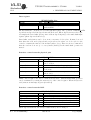
This chapter describes the interrupt-capable 16-bit general-purpose I/O block for VS DSP.
Note that in VS1000, pin function is partly handled also by the System Controller:
GPIOn MODE register bits control whether output data for a GPIO pin is taken from
a peripheral function (mode=“1”) or the GPIO controller (mode=“0”).
4.3.2
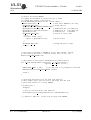
Reg
0
1
2
3
4
5
6
7
8
9
10
Registers
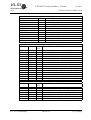
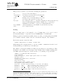
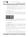
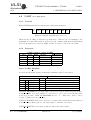
Interruptable General I/O registers, prefix GPIOx
Type Reset Abbrev
Description
r/w
0
DDR
Data direction
r/w
0
ODATA
Data output
r
0
IDATA
Data input (I/O pin state)
r/w
0
INT FALL
Falling edge interrupt enable
r/w
0
INT RISE
Rising edge interrupt enable
r/w
0
INT PEND
Interrupt pending source
w
0
SET MASK
Data set (→ 1) mask
w
0
CLEAR MASK Data clear (→ 0) mask
r/w
0
BIT CONF
Bit engine config 0 and 1
r/w
0
BIT ENG0
Bit engine 0 read/write
r/w
0
BIT ENG1
Bit engine 1 read/write
Data Direction GPIOx DDR
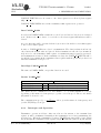
The data direction register (DDR) configures the directions of each of the 16 I/O pins.
A bit set to 1 in the DDR turns the corresponding I/O pin to output mode, while a bit
set to 0 sets the pin to input mode. The register is set to all zeros in reset, i.e. all pins
are inputs by default. The current state of the DDR can also be read.
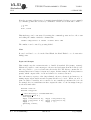
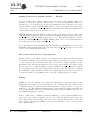
Output Data GPIOx ODATA
A write sets the data register value. Change in bits that are configured as outputs are
reflected in the outputs. A read returns the state of data register value.
Note: configuring a pin as input should not reset the state of the corresponding data
register bit. If the data register is first written 0xffff and then all pins are configured as
outputs by writing 0xffff to DDR, all outputs should go to the high state.
Rev. 0.15 Preliminary
2008-06-30
Page 51(87)