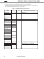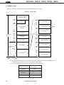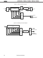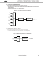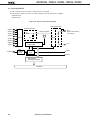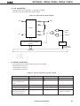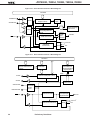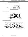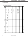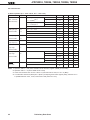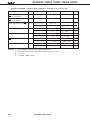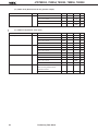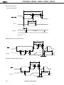
1
PRELIMINARY DATA SHEET
MOS INTEGRATED CIRCUIT
µPD780053,780054,780055,780056,780058
8-BIT SINGLE-CHIP MICROCONTROLLER
DESCRIPTION
The µPD780053,780054,780055,780056 and 780058 are members of the µPD780058 subseries in the 78K/0
series. These microcontrollers suppress the EMI (Electro Magnetic Interference) noise internally generated to the
lower level than the existing µPD78054 subseries. In addition, they have many peripheral hardware units such as an
8-bit resolution A/D converter, 8-bit resolution D/A converter, timers, serial interface, real-time output ports, and
interrupt functions.
A flash memory model that can operate on the same voltage as the mask ROM models, µPD78F0058, and various
development tools are now under development.
The funcitons are explaned in detail in the following User's Manuals. Be sure to read these manuals when
designing your system.
µPD780058, 780058Y Subseries User's Manual : U12013E
78K/0 Series User's Manual - Instruction
: U12326E
FEATURES
• Internal high-capacity ROM & RAM
Item
Program Memory
Part Number
•
•
•
•
•
•
•
•
(ROM)
µPD780053
24K bytes
µPD780054
32K bytes
µPD780055
40K bytes
µPD780056
48K bytes
µPD780058
60K bytes
Data Memory
Internal high-speed RAM
Internal buffer RAM
Internal expanded RAM
1024 bytes
32 bytes
None
1024 bytes
External memory expansion space: 64K bytes
Minimum instruction execution time changeable from high speed (0.4 µs) to ultra low-speed (122 µs)
I/O ports: 68 pins (N-ch open-drain : 4 pins)
8-bit resolution A/D converter : 8 channels (VDD = 2.7 to 5.5 V)
8-bit resolution D/A converter : 2 channels (VDD = 2.7 to 5.5 V)
Serial interface
: 3 channels
Timer
: 5 channels
Operating voltage range
: VDD = 1.8 to 5.5 V
APPLICATION FIELDS
Car audio systems, cellular phones, pagers, printers, AV systems, cameras, PPCs, and vending machines
The information in this document is subject to change without notice.
Document No. U12182EJ1V1DS00 (1st edition)
Date Published January 1999 N CP(K)
Printed in Japan
The mark
shows major revised points.
©
1997
µPD780053, 780054, 780055, 780056, 780058
ORDERING INFORMATION
Part Number
µPD780053GC-×××-8BT
80-pin plastic QFP (14 × 14 mm)
µPD780053GK-×××-BE9
80-pin plastic TQFP (fine pitch) (12 × 12 mm)
µPD780054GC-×××-8BT
80-pin plastic QFP (14 × 14 mm)
µPD780054GK-×××-BE9
80-pin plastic TQFP (fine pitch) (12 × 12 mm)
µPD780055GC-×××-8BT
80-pin plastic QFP (14 × 14 mm)
µPD780055GK-×××-BE9
80-pin plastic TQFP (fine pitch) (12 × 12 mm)
µPD780056GC-×××-8BT
80-pin plastic QFP (14 × 14 mm)
µPD780056GK-×××-BE9
80-pin plastic TQFP (fine pitch) (12 × 12 mm)
µPD780058GC-×××-8BT
80-pin plastic QFP (14 × 14 mm)
µPD780058GK-×××-BE9
80-pin plastic TQFP (fine pitch) (12 × 12 mm)
Remark
2
Package
××× indicates ROM code suffix.
Preliminary Data Sheet
µPD780053, 780054, 780055, 780056, 780058
78K/0 SERIES PRODUCT DEVELOPMENT
The following shows the 78K/0 Series products development. Subseries name are shown inside frames.
Products in
mass production
Products under
development
Y subseries products are compatible with I2C bus.
Control
100-pin
100-pin
100-pin
100-pin
80-pin
80-pin
80-pin
64-pin
64-pin
64-pin
64-pin
64-pin
64-pin
64-pin
42/44-pin
µPD78075B
µPD78078
µ PD78070A
µ PD780058
µ PD78058F
µ PD78054
µ PD780034
µ PD780024
µ PD78014H
µPD78018F
µPD78014
µPD780001
µPD78002
µPD78083
EMI-noise reduced version of the µPD78078
µPD78078Y
µPD78070AY
µ PD780018YNote
µ PD780058YNote
µ PD78058FY
µ PD78054Y
µ PD780034Y
µPD780024Y
µ PD78018FY
µ PD78014Y
µPD78002Y
A timer was added to the µPD78054 and external interface was enhanced
ROM-less version of the µPD78078
Serial I/O of the µPD78078Y was enhanched and the function is limited
Serial I/O of the µPD78054 was enhanced and EMI-noise was reduced
EMI-noise reduced version of the µPD78054
UART and D/A converter were added to the µPD78014 and I/O was enchanced
A/D converter of the µPD780024 was enchanced
Serial I/O of the µPD78018F was added
EMI-noise reduced version of µ PD78018F
Low-voltage (1.8 V) operation version of the µ PD78014, with larger
selection of ROM and RAM capacities
An A/D converter and 16-bit timer were added to the µPD78002
An A/D converter was added to the µPD78002
Basic subseries for control
On-chip UART, capable of operating at low voltage (1.8 V)
Inverter control
64-pin
µPD780988
On-chip inverter control circuit and UART. EMI-noise was reduced.
FIPTM drive
78K/0
Series
100-pin
100-pin
80-pin
80-pin
I/O and FIP C/D of the µPD78044F were enhanced, Display output total: 53
I/O and FIP C/D of the µPD78044H were enhanced, Display output total: 48
N-ch open drain was added to the µPD78044F, Display output total: 34
µPD780208
µ PD780228
µPD78044H
µPD78044F
Basic subseries for driving FIP, Display output total: 34
LCD drive
100-pin
100-pin
100-pin
µ PD780308
µPD780308Y
The SIO of the µPD78064 was enhanced and ROM, RAM capacity increased
µ PD78064B
µPD78064
µ PD78064Y
EMI-noise reduced version of the µPD78064
Basic subseries for driving LCDs, On-chip UART
IEBusTM supported
80-pin
80-pin
µPD78098B
µ PD78098
EMI-noise reduced version of the µ PD78098
An IEBus controller was added to the µ PD78054
Meter control
80-pin
µPD780973
On-chip controller/driver for automotive meter drive
Note Under planning
Preliminary Data Sheet
3
µPD780053, 780054, 780055, 780056, 780058
The following lists the main functional differences between subseries products.
Function
Subseries Name
Control
ROM
Capacity
µPD78075B
32 K - 40K
µPD78078
48 K - 60K
µPD78070A
–
µPD780058
24 K - 60 K
µPD78058F
48 K - 60 K
µPD78054
16 K - 60 K
µPD780034
8 K - 32 K
Timer
8-bit 16-bit Watch WDT
8-bit 10-bit
A/D A/D
8-bit
D/A
4ch
8ch
2ch
1ch
1ch
1ch
–
2ch
Serial
Interface
3ch (UART : 1ch)
–
8ch
8ch
–
–
88
1.8 V
61
2.7 V
3ch (time division
UART: 1ch)
68
1.8 V
3ch (UART: 1ch)
69
2.7 V
3ch (UART: 1ch, time
2ch
µPD78014
8 K - 32 K
µPD780001
8K
µPD78002
8 K - 16 K
51
1.8 V
division 3-wire: 1ch)
µPD78014H
8 K - 60 K
VDD MIN. External
Value Expansion
2.0 V
µPD780024
µPD78018F
I/O
53
2.7 V
–
–
µPD78083
1ch
1ch
–
–
8ch
39
–
53
1ch (UART: 1ch)
33
1.8 V
µPD780988
32 K - 60 K
3ch
Note
–
1ch
–
8ch
–
3ch (UART: 2ch)
47
4.0 V
FIP
µPD780208
32 K - 60 K
2ch
1ch
1ch
1ch
8ch
–
–
2ch
74
2.7 V
drive
µPD780228
48 K - 60 K
3ch
–
–
1ch
72
4.5 V
µPD78044H
32 K - 48 K
2ch
1ch
1ch
68
2.7 V
µPD78044F
16 K - 40 K
µPD780308
48 K - 60 K
57
2.0 V
µPD78064B
32 K
µPD78064
16 K - 32 K
IEBus
µPD78098B
40 K - 60 K
3ch (UART : 1 ch)
69
2.7 V
supported
µPD78098
32 K - 60 K
LV
µPD78P0914
32 K
2ch
54
4.5 V
Inverter
–
control
LCD
drive
2ch
2ch
1ch
1ch
1ch
8ch
–
–
3ch (time division
UART: 1ch)
2ch (UART : 1 ch)
2ch
1ch
1ch
1ch
8ch
–
2ch
6ch
–
–
1ch
8ch
–
–
Note 16-bit timer : 2 channels
10-bit timer : 1 channel
4
–
Preliminary Data Sheet
–
µPD780053, 780054, 780055, 780056, 780058
OVERVIEW OF FUNCTION
Product Name
Item
Internal
memory
ROM
High-speed RAM
Buffer RAM
Expanded RAM
Memory space
General registers
Minimum instruction execution
time
When main system
clock selected
When subsystem
clock selected
µPD780053
µPD780054
µPD780055
µPD780056
µPD780058
24K bytes
32K bytes
40K bytes
1024 bytes
32 bytes
48K bytes
60K bytes
None
64 K bytes
8 bits × 32 registers (8 bits × 8 registers × 4 banks)
On-chip minimum instruction execution time cycle modification function
1024 bytes
0.4 µs/0.8 µs/1.6 µs/3.2 µs/6.4 µs/12.8 µs (at 5.0 MHz operation)
122 µs (at 32.768 kHz operation)
Instruction set
•
•
•
•
I/O ports
Total
• CMOS input
• CMOS I/O
• N-ch open-drain I/O
A/D converter
D/A converter
Serial interface
•
•
•
•
Timer
•
•
•
•
Timer output
3 (14-bit PWM output × 1)
Clock output
19.5 kHz, 39.1 kHz, 78.1 kHz, 156 kHz, 313 kHz, 625 kHz, 1.25 MHz, 2.5 MHz, 5.0 MHz
(at main system clock: 5.0 MHz operation)
32.768 kHz (at subsystem clock: 32.768 kHz operation)
Buzzer output
1.2 kHz, 2.4 kHz, 4.9 kHz, 9.8 kHz (at main system clock: 5.0 MHz operation)
Vectored
interrupt
sources
16-bit operation
Multiplication/division (8 bits × 8 bits,16 bits ÷ 8 bits)
Bit manipulation (set, reset, test, boolean operation)
BCD correction, etc.
: 68
: 2
: 62
: 4
8-bit resolution × 8 channels (VDD = 2.7 to 5.5 V)
8-bit resolution × 2 channels (VDD = 2.7 to 5.5 V)
3-wire serial I/O/SBI/2-wire serial I/O mode selectable: 1 channel
3-wire serial I/O mode (on-chip max. 32 bytes automatic data transmit/receive function):
1 channel
• 3-wire/serial I/O/UART mode (on-chip time division transfer function) selectable:
1 channel
16-bit timer/event counter
8-bit timer/event counter
Watch timer
Watchdog timer
:
:
:
:
1
2
1
1
channel
channels
channel
channel
Maskable
Internal interrupt : 13, external interrupt : 6
Non-maskable
Internal interrupt : 1
Software
1
Test input
Internal : 1, external : 1
Supply voltage
VDD = 1.8 to 5.5 V
Operating ambient temperature
TA = –40 to +85°C
Package
• 80-pin plastic QFP (14 × 14 mm)
• 80-pin plastic TQFP (fine pitch) (12 × 12 mm)
Preliminary Data Sheet
5
µPD780053, 780054, 780055, 780056, 780058
CONTENTS
1.
PIN CONFIGURATION (TOP VIEW) ..............................................................................................
7
2.
BLOCK DIAGRAM .........................................................................................................................
9
3.
PIN FUNCTIONS ............................................................................................................................ 10
3.1
PORT PINS .............................................................................................................................................. 10
3.2
OTHER PINS ............................................................................................................................................ 12
3.3
PIN I/O CIRCUITS AND RECOMMENDED CONNECTION OF UNUSED PINS ................................. 14
4.
MEMORY SPACE ............................................................................................................................ 18
5.
PERIPHERAL HARDWARE FUNCTION FEATURES .................................................................. 19
6.
5.1
PORTS ...................................................................................................................................................... 19
5.2
CLOCK GENERATOR ............................................................................................................................. 20
5.3
TIMER/EVENT COUNTER ...................................................................................................................... 20
5.4
CLOCK OUTPUT CONTROL CIRCUIT ................................................................................................. 23
5.5
BUZZER OUTPUT CONTROL CIRCUIT ................................................................................................ 23
5.6
A/D CONVERTER .................................................................................................................................... 24
5.7
D/A CONVERTER .................................................................................................................................... 25
5.8
SERIAL INTERFACES ............................................................................................................................ 25
5.9
REAL-TIME OUTPUT PORT FUNCTIONS ............................................................................................ 27
INTERRUPT FUNCTIONS .............................................................................................................. 28
6.1
INTERRUPT FUNCTIONS ....................................................................................................................... 28
6.2
TEST FUNCTIONS .................................................................................................................................. 32
7.
EXTERNAL DEVICE EXPANSION FUNCTIONS .......................................................................... 33
8.
STANDBY FUNCTION .................................................................................................................... 33
9.
RESET FUNCTION .......................................................................................................................... 33
10. INSTRUCTION SET ......................................................................................................................... 34
11. ELECTRICAL SPECIFICATIONS ................................................................................................... 36
12. PACKAGE DRAWINGS .................................................................................................................. 63
APPENDIX A. DEVELOPMENT TOOLS ........................................................................................... 65
APPENDIX B. RELATED DOCUMENTS ........................................................................................... 68
6
Preliminary Data Sheet
µPD780053, 780054, 780055, 780056, 780058
1. PIN CONFIGURATION (TOP VIEW)
• 80-pin plastic QFP (14 × 14 mm)
µPD780053GC-×××-8BT, 780054GC-×××-8BT, 780055GC-×××-8BT, 780056GC-×××-8BT, 780058GC-×××-8BT
• 80-pin plastic TQFP (fine pitch) (12 × 12 mm)
P00/INTP0/TI00
P01/INTP1/TI01
P02/INTP2
P03/INTP3
P04/INTP4
P05/INTP5
VSS0
VDD1
X2
X1
IC
XT2
XT1/P07
VDD0
AVREF0
P10/ANI0
P11/ANI1
P12/ANI2
P13/ANI3
P14/ANI4
µPD780053GK-×××-BE9, 780054GK-×××-BE9, 780055GK-×××-BE9, 780056GK-×××-BE9, 780058GK-×××-BE9
7
54
P122/RTP2
P70/SI2/RxD0
8
53
P121/RTP1
P71/SO2/TxD0
9
52
P120/RTP0
P72/SCK2/ASCK
10
51
P37
P20/SI1
11
50
P36/BUZ
P21/SO1
12
49
P35/PCL
P22/SCK1
13
48
P34/TI2
P23/STB/TxD1
14
47
P33/TI1
P24/BUSY/RxD1
15
46
P32/TO2
P25/SI0/SB0
16
45
P31/TO1
P26/SO0/SB1
17
44
P30/TO0
P27/SCK0
18
43
P67/ASTB
P40/AD0
19
42
P66/WAIT
P41/AD1
41
20
21 22 23 24 25 26 27 28 29 30 31 32 33 34 35 36 37 38 39 40
Cautions 1.
2.
RESET
P65/WR
P64/RD
P63
P123/RTP3
AVREF1
P62
55
P61
6
P60
P124/RTP4
P131/ANO1
P57/A15
56
P56/A14
5
VSS1
P125/RTP5
P130/ANO0
P55/A13
57
P54/A12
4
P53/A11
P126/RTP6
AVSS
P52/A10
58
P51/A9
3
P50/A8
P127/RTP7
P17/ANI7
P47/AD7
59
P46/AD6
2
P45/AD5
P16/ANI6
P44/AD4
80 79 78 77 76 75 74 73 72 71 70 69 68 67 66 65 64 63 62 61
60
P43/AD3
1
P42/AD2
P15/ANI5
Directly connect the IC (Internally Connected) pins to VSS0 or VSS1.
Connect the AVSS pin to VSS0.
Remarks 1. ××× indicates ROM code suffix.
2. If the microcontroller is used in an application where the noise generated from the microcontroller
must be suppressed, it is recommended that power be supplied to VDD0 and VDD1 from separate
sources, and that VSS0 and VSS1 be connected to separate group lines, to improve noise immunity.
Preliminary Data Sheet
7
µPD780053, 780054, 780055, 780056, 780058
A8-A15
: Address Bus
P130, P131
: Port13
AD0-AD7
: Address/Data Bus
PCL
: Programmable Clock
ANI0-ANI7
: Analog Input
RD
: Read Strobe
ANO0, ANO1
: Analog Output
RESET
: Reset
ASCK
: Asychronous Serial Clock
RTP0-RTP7
: Real-Time Output Port
ASTB
: Address Strobe
RxD0, RxD1
: Receive Data
AVREF0, 1
: Analog Reference Voltage
SB0, SB1
: Serial Bus
AVSS
: Analog Ground
SCK0-SCK2
: Serial Clock
BUSY
: Busy
SI0-SI2
: Serial Input
BUZ
: Buzzer Clock
SO0-SO2
: Serial Output
IC
: Internally Connected
STB
: Strobe
INTP0-INTP5
: Interrupt from Peripherals
TI00, TI01
: Timer Input
P00-P05, P07
: Port0
TI1, TI2
: Timer Input
P10-P17
: Port1
TO0-TO2
: Timer Output
P20-P27
: Port2
TxD0, TxD1
: Transmit Data
P30-P37
: Port3
VDD0, VDD1
: Power Supply
P40-P47
: Port4
VSS0, VSS1
: Ground
P50-P57
: Port5
WAIT
: Wait
P60-P67
: Port6
WR
: Write Strobe
P70-P72
: Port7
X1, X2
: Crystal (Main System Clock)
P120-P127
: Port12
XT1, XT2
: Crystal (Subsystem Clock)
8
Preliminary Data Sheet
µPD780053, 780054, 780055, 780056, 780058
2. BLOCK DIAGRAM
TO0/P30
TI00/INTP0/P00
TI01/INTP1/P01
16-bit TIMER/
EVENT COUNTER
TO1/P31
TI1/P33
8-bit TIMER/
EVENT COUNTER 1
TO2/P32
TI2/P34
8-bit TIMER/
EVENT COUNTER 2
PORT0
P00
P01-P05
P07
PORT1
P10-P17
PORT2
P20-P27
PORT3
P30-P37
PORT4
P40-P47
PORT5
P50-P57
PORT6
P60-P67
PORT7
P70-P72
PORT12
P120-P127
PORT13
P130,P131
REAL-TIME
OUTPUT PORT
RTP0/P120RTP7/P127
WATCHDOG TIMER
WATCH TIMER
SI0/SB0/P25
SO0/SB1/P26
SCK0/P27
SERIAL
INTERFACE 0
78K/0
CPU CORE
SI1/P20
SO1/P21
SCK1/P22
STB/TxD1/P23
BUSY/RxD1/P24
SERIAL
INTERFACE 1
BUSY/RxD1/P24
STB/TxD1/P23
SI2/RxD0/P70
SO2/TxD0/P71
SCK2/ASCK/P72
SERIAL
INTERFACE 2
ROM
RAM
ANI0/P10ANI7/P17
AVSS
AVREF0
ANO0/P130,
ANO1/P131
AVSS
A/D CONVERTER
D/A CONVERTER
AVREF1
INTP0/P00INTP5/P05
BUZ/P36
PCL/P35
EXTERNAL
ACCESS
AD0/P40AD7/P47
A8/P50A15/P57
RD/P64
WR/P65
WAIT/P66
ASTB/P67
SYSTEM
CONTROL
RESET
X1
X2
XT1/P07
XT2
INTERRUPT
CONTROL
BUZZER OUTPUT
CLOCK OUTPUT
CONTROL
VDD0,
VDD1
VSS0,
IC
VSS1
Remark The internal ROM and RAM capacities differ depending on the product.
Preliminary Data Sheet
9
µPD780053, 780054, 780055, 780056, 780058
3. PIN FUNCTIONS
3.1 PORT PINS (1/2)
Pin Name
P00
Input
P01
Input/
output
P02
After
Reset
DualFunction Pin
Input only
Input
INTP0/TI00
Input/output can be specified bit-wise.
When used as an input port, on-chip pull-up
resistor can be used by software.
Input
INTP1/TI01
Function
I/O
Port 0
7-bit input/output port
INTP2
P03
INTP3
P04
INTP4
P05
INTP5
P07Note 1
Input
P10-P17
Input/
output
P20
Input/
output
P21
P22
P23
Input only
Input
XT1
Port 1
8-bit input/output port.
Input/output can be specified bit-wise.
When used as an input port, on-chip pull-up resistor can be used by
softwareNote 2.
Input
ANI0-ANI7
Port 2
8-bit input/output port.
Input/output can be specified bit-wise.
When used as an input port, on-chip pull-up resistor can be used by
software.
Input
SI1
SO1
SCK1
STB/TxD1
P24
BUSY/RxD1
P25
SI0/SB0
P26
SO0/SB1
P27
SCK0
Input/
output
P30
P31
P32
P33
Port 3
8-bit input/output port.
Input/output can be specified bit-wise.
When used as an input port, on-chip pull-up resistor can be used by
software.
Input
TO0
TO1
TO2
TI1
P34
TI2
P35
PCL
P36
BUZ
P37
—
P40-P47
Input/
output
Port 4
8-bit input/output port.
Input/output can be specified in 8-bit unit.
When used as an input port, on-chip pull-up resistor can be used by
software. Test input flag (KRIF) is set to 1 by falling edge detection.
Input
AD0-AD7
Notes 1. When using the P07/XT1 pins as an input port, set 1 in the bit 6 (FRC) of the processor clock control
register (PCC). On-chip feedback resistor of the subsystem clock oscillator should not be used.
2. When using the P10/ANI0 to P17/ANI7 pins as the A/D converter analog input pins, set port 1 to input
mode. Use of the on-chip pull-up resistor is cancelled automatically.
10
Preliminary Data Sheet
µPD780053, 780054, 780055, 780056, 780058
3.1 PORT PINS (2/2)
Pin Name
I/O
Function
P50-P57
Input/
output
Port 5
8-bit input/output port.
LED can be driven directly.
Input/output can be specified bit-wise.
When used as an input port, on-chip pull-up resistor can be used by software.
P60
Input/
output
Port 6
8-bit input/outport port. Input/output can be
specified bit-wise.
P61
P62
P63
N-ch open-drain input/
output port. On-chip pullup resistor can be used
by mask option. LED can
be driven directly.
After
Reset
DualFunction Pin
Input
A8-A15
Input
—
RD
When used as an input
port, on-chip pull-up
resistor can be used by
software.
P64
P65
P66
WR
WAIT
ASTB
P67
P70
P71
Input/
output
P72
Port 7
3-bit input/output port.
Input/output can be specified bit-wise.
When used as an input port, on-chip pull-up resistor can be used by software.
Input
SI2/RxD0
SO2/TxD0
SCK2/ASCK
P120-P127
Input/
output
Port 12
8-bit input/output port.
Input/output can be specified bit-wise.
When used as an input port, on-chip pull-up resistor can be used by software.
Input
RTP0-RTP7
P130, P131
Input/
output
Port 13
2-bit input/output port.
Input/output can be specified bit-wise.
When used as an input port, on-chip pull-up resistor can be used by software.
Input
ANO0, ANO1
Preliminary Data Sheet
11
µPD780053, 780054, 780055, 780056, 780058
3.2 OTHER PINS (1/2)
Pin Name
INTP0
I/O
Input
INTP1
Function
External interrupt request input for which the effective edge (rising edge,
falling edge, or both rising edge and falling edge) can be specified.
After
Reset
DualFunction Pin
Input
P00/TI00
P01/TI01
INTP2
P02
INTP3
P03
INTP4
P04
INTP5
P05
SI0
Input
Serial interface serial data input.
Input
P25/SB0
SI1
P20
SI2
P70/RxD
SO0
Output
Serial interface serial data output.
Input
P26/SB1
SO1
P21
SO2
P71/TxD
SB0
SB1
SCK0
SCK1
Input/
output
Serial interface serial data input/output.
Input/
output
Serial interface serial clock input/ output
Input
P25/SI0
P26/SO0
Input
P27
P22
P72/ASCK
SCK2
Output
Serial interface automatic transmit/receive strobe output.
Input
P23/TxD1
BUSY
Input
Serial interface automatic transmit/receive busy input.
Input
P24/RxD1
RxD0
Input
Asynchronous serial interface serial data input.
Input
P70/SI2
STB
P24/BUSY
RxD1
TxD0
Output
Asynchronous serial interface serial data output.
Input
P71/SO2
P23/STB
TxD1
ASCK
Input
Asynchronous serial interface serial clock input.
Input
P72/SCK2
TI00
Input
External count clock input to the 16-bit timer (TM0)
Input
P00/INTP0
P01/INTP1
TI01
Capture trigger signal input to the capture register (CR00)
TI1
External count clock input to the 8-bit timer (TM1)
P33
TI2
External count clock input to the 8-bit timer (TM2)
P34
TO0
Output
16-bit timer (TM0) output (dual-function as 14-bit PWM output)
Input
P30
TO1
8-bit timer (TM1) output
P31
TO2
8-bit timer (TM2) output
P32
PCL
Output
Clock output (for main system clock, subsystem clock trimming).
Input
P35
BUZ
Output
Buzzer output.
Input
P36
RTP0-RTP7
Output
Real-time output port by which data is output in synchronization with a trigger.
Input
P120-P127
AD0-AD7
Input/
output
Low-order address/data bus at external memory expansion.
Input
P40-P47
A8-A15
Output
High-order address bus at external memory expansion.
Input
P50-P57
RD
Output
External memory read operation strobe signal output.
Input
P64
WR
12
External memory write operation strobe signal output.
Preliminary Data Sheet
P65
µPD780053, 780054, 780055, 780056, 780058
3.2 OTHER PINS (2/2)
After
Reset
DualFunction Pin
Wait insertion at external memory access.
Input
P66
Strobe output which latches the address information output at port 4 to access
external memory.
Input
P67
A/D converter analog input.
Input
P10-P17
D/A converter analog output.
Input
P130, P131
A/D converter reference voltage input (dual-function as analog power supply).
—
—
D/A converter reference voltage input.
—
—
A/D converter, D/A converter ground potential. Use at the same potential as
VSS0.
—
—
Input
System reset input.
—
—
X1
Input
Main system clock oscillation crystal connection.
—
—
X2
—
—
—
XT1
Input
Input
P07
XT2
—
—
—
VDD0
—
Port block positive power supply.
—
—
VSS0
—
Port block ground potential.
—
—
VDD1
—
Positive power supply (except for port and analog blocks).
—
—
VSS1
—
Ground potiential (except for port and analog blocks).
—
—
IC
—
Internally connected. Connect to VSS0 or VSS1 directly.
—
—
Pin Name
I/O
WAIT
Input
ASTB
Output
ANI-ANI7
Input
ANO0, ANO1
Output
AVREF0
Input
AVREF1
Input
AVSS
—
RESET
Function
Subsystem clock oscillation crystal connection.
Preliminary Data Sheet
13
µPD780053, 780054, 780055, 780056, 780058
3.3 PIN I/O CIRCUITS AND RECOMMENDED CONNECTION OF UNUSED PINS
The input/output circuit type of each pin and recommended connection of unused pins are shown in Table 3-1.
For the input/output circuit configuration of each type, see Figure 3-1.
Table 3-1. Input/Output Circuit Type of Each Pin (1/2)
Pin Name
Input/Output
Circuit Type
I/O
P00/INTP0/TI00
2
Input
P01/INTP1/TI01
8-C
Input/output
16
Input
P10/ANI0-P17/ANI7
11-D
Input/output
P20/SI1
8-C
P21/SO1
5-H
P22/SCK1
8-C
P23/STB/TxD1
5-H
P24/BUSY/RxD1
8-C
P25/SI0/SB0
10-B
Recommended Connection when Not Used
Connect to VSS0.
Independently connect to VSS0 through resistor.
P02/INTP2
P03/INTP3
P04/INTP4
P05/INTP5
P07/XT1
Connect to VDD0.
Independently connect to VDD0 or VSS0 through resistor.
P26/SO0/SB1
P27/SCK0
P30/TO0
5-H
P31/TO1
P32/TO2
P33/TI1
8-C
P34/TI2
P35/PCL
5-H
P36/BUZ
P37
P40/AD0-P47/AD7
5-N
Independently connect to VDD0 through resistor.
P50/A8-P57/A15
5-H
Independently connect to VDD0 or VSS0 through resistor.
P60-P63
13-J
Independently connect to VDD0 through resistor.
P64/RD
5-H
Independently connect to VDD0 or VSS0 through resistor.
P65/WR
P66/WAIT
P67/ASTB
14
Preliminary Data Sheet
µPD780053, 780054, 780055, 780056, 780058
Table 3-1. Input/Output Circuit Type of Each Pin (2/2)
Pin Name
P70/SI2/RxD0
Input/Output
Circuit Type
I/O
8-C
Input/
P71/SO2/TxD0
5-H
output
P72/SCK2/ASCK
8-C
P120/RTP0-
5-H
Recommended Connection when Not Used
Independently connect to VDD0 or VSS0 through resistor.
P127/RTP7
P130/ANO0 ,
12-C
Independently connect to VSS0 through resistor.
P131/ANO1
RESET
2
Input
XT2
16
—
AVREF0
—
—
Leave open.
Connect to VSS0.
AVREF1
Connect to VDD0.
AVSS
Connect to VSS0.
IC
Connect to VSS0 or VSS1 directly.
Preliminary Data Sheet
15
µPD780053, 780054, 780055, 780056, 780058
Figure 3-1. Pin Input/Output Circuits (1/2)
Type 2
Type 8-C
VDD0
pullup
enable
P-ch
IN
VDD0
data
P-ch
IN/OUT
Schmitt-Triggered Input with Hysteresis Characteristic
VDD0
Type 5-H
pullup
enable
output
disable
N-ch
VSS0
VDD0
Type 10-B
pullup
enable
P-ch
P-ch
VDD0
data
VDD0
data
P-ch
P-ch
IN/OUT
output
disable
IN/OUT
open drain
output disable
N-ch
VSS0
N-ch
VSS0
input
enable
Type 5-N
pullup
enable
pullup
enable
P-ch
IN/OUT
N-ch
output
disable
Comparator
VSS0
input
enable
16
P-ch
P-ch
IN/OUT
output
disable
P-ch
VDD0
data
VDD0
data
V DD0
Type 11-D
VDD0
Preliminary Data Sheet
N-ch
P-ch
+
-
VSS0
N-ch
VSS0
VREF (Threshold Voltage)
µPD780053, 780054, 780055, 780056, 780058
Figure 3-1. Pin Input/Output Circuits (2/2)
VDD0
Type 12-C
pullup
enable
Type 16
feed back
P-ch
cut-off
VDD0
data
P-ch
P-ch
IN/OUT
output
disable
input
enable
N-ch
VSS0
P-ch
XT1
Analog Output
Voltage
N-ch
XT2
VSS0
Type 13-J
VDD0
Mask
Option
IN/OUT
data
output disable
N-ch
VSS0
VDD0
RD
P-ch
Middle-High Voltage Input Buffer
Preliminary Data Sheet
17
µPD780053, 780054, 780055, 780056, 780058
4. MEMORY SPACE
Figure 4-1 shows the µPD780053/780054/780055/780056/780058 memory map.
Figure 4-1. Memory Map
FFFFH
Special Function Registers
(SFR) 256 × 8 bits
FF00H
FEFFH
FEE0H
FEDFH
FA7FH
General Registers
32 × 8 bits
Use Prohibited
F800H
F7FFH
Internal High-Speed
RAM Note 3
Internal Expanded RAM
1024 × 8 bits
F400H
F3FFH
FB00H
FAFFH
Use Prohibited Note 2
Use Prohibited
Data Memory
Space
FAE0H
FADFH
FAC0H
FABFH
Note 1
Internal Buffer RAM
32 × 8 bits
F000H
nnnnH
Program Area
1000H
0FFFH
Use Prohibited
FA80H
FA7FH
CALLF Entry Area
0800H
07FFH
Program Area
External Memory
0080H
007FH
Program Memory
Space
nnnnH + 1
nnnnH
CALLT Table Area
Internal ROM
Note 3
0040H
003FH
Vector Table Area
0000H
0000H
Notes 1. µPD780058 only
2. When the external device expansion function is used with the µPD780058, set the internal ROM capacity
to 56K bytes or less using the memory size switching register (IMS).
3. The internal ROM capacity depends on the products (see the next table).
Relevant Product Name
18
Internal ROM Last Address
nnnnH
µPD780053
5FFFH
µPD780054
7FFFH
µPD780055
9FFFH
µPD780056
BFFFH
µPD780058
EFFFH
Preliminary Data Sheet
µPD780053, 780054, 780055, 780056, 780058
5. PERIPHERAL HARDWARE FUNCTION FEATURES
5.1 PORTS
The following three types of I/O ports are available.
• CMOS input (P00, P07)
:
2
• CMOS input/output (P01-P05, port 1-port 5, P64-P67, port 7, port 12, port 13)
:
62
• N-channel open-drain input/output (P60-P63)
:
4
:
68
Total
Table 5-1. Port Functions
Name
Port 0
Pin Name
Function
P00, P07
Dedicated input port pins
P01-P05
Input/output port pins. Input/output specifiable bit-wise.
When used as input port pins, on-chip pull-up resistor can be used by software.
Port 1
P10-P17
Input/output port pins. Input/output specifiable bit-wise.
When used as input port pins, on-chip pull-up resistor can be used by software.
Port 2
P20-P27
Port 3
P30-P37
Input/output port pins. Input/output specifiable bit-wise.
When used as input port pins, on-chip pull-up resistor can be used by software.
Input/output port pins. Input/output specifiable bit-wise.
When used as input port pins, on-chip pull-up resistor can be used by software.
Port 4
P40-P47
Input/output port pins. Input/output specifiable in 8-bit units.
When used as input port pins, on-chip pull-up resistor can be used by software.
Port 5
P50-P57
Test flag (KRIF) is set to 1 by falling edge detection.
Input/output port pins. Input/output specifiable bit-wise.
When used as input port pins, on-chip pull-up resistor can be used by software.
LED direct drive capability.
Port 6
P60-P63
N-channel open-drain input/output port pins. Input/output specifiable bit-wise.
On-chip pull-up resistor can be used by mask option.
LED direct drive capability.
P64-P67
Input/output port pins. Input/output specifiable bit-wise.
When used as input port pins, on-chip pull-up resistor can be used by software.
Port 7
P70-P72
Input/output port pins. Input/output specifiable bit-wise.
Port 12
P120-P127
Input/output port pins. Input/output specifiable bit-wise.
When used as input port pins, on-chip pull-up resistor can be used by software.
When used as input port pins, on-chip pull-up resistor can be used by software.
Port 13
P130, P131
Input/output port pins. Input/output specifiable bit-wise.
When used as input port pins, on-chip pull-up resistor can be used by software.
Preliminary Data Sheet
19
µPD780053, 780054, 780055, 780056, 780058
5.2 CLOCK GENERATOR
Two types of generators, a main system clock generator and a subsystem clock generator, are avaibable.
The minimum instruction execution time can also be changed.
• 0.4 µs/0.8 µs/1.6 µs/3.2 µs/6.4 µs/12.8 µs (main system clock: at 5.0 MHz operation)
• 122 µs (subsystem clock: at 32.768 kHz operation)
Figure 5-1. Clock Generator Block Diagram
XT1/P07
XT2
Subsystem
Clock
Oscillator
fXT
Watch Timer, Clock
Output Function
Prescaler
1
X1
X2
Main System fX
Clock
Oscillator
Selector
STOP
Clock to Peripheral
Hardware
Prescaler
fXX
fXX fXX fXX
2 22 23
Scaler
2
fX
2
fXX fXT
24 2
Selector
Standby
Control
Circuit
Wait Control
Circuit
CPU Clock
(fCPU)
To INTP0
Sampling Clock
5.3 TIMER/EVENT COUNTER
The following five channels of the timer/event counter are available.
• 16-bit timer/event counter : 1 channel
• 8-bit timer/event counter
: 2 channels
• Watch timer
: 1 channel
• Watchdog timer
: 1 channel
Table 5-2. Operations of Timer/Event Counter
Operation
mode
Function
16-Bit Timer/
Event Counter
8-Bit Timer/
Event Counter
Watch Timer
Watchdog Timer
Interval timer
1 channel
2 channels
1 channel
1 channel
External event counter
1 channel
2 channels
—
—
Timer output
1 output
2 outputs
—
—
PWM output
1 output
—
—
—
Pulse width measurement
1 input
—
—
—
Square wave output
1 output
2 outputs
—
—
Ono-shot pulse output
1 output
—
—
—
2
2
2
1
Interrupt request
20
Preliminary Data Sheet
µPD780053, 780054, 780055, 780056, 780058
Figure 5-2. 16-Bit Timer/Event Counter Block Diagram
Internal Bus
INTP1
TI01/P01/INTP1
16-Bit Capture/
Compare Register
(CR00)
Selector
INTTM00
PWM pulse
Output
Control
Circuit
Match
Watch Timer
Output
Output Control
Circuit
TO0/P30
2fXX
fXX
Selector
fXX/2
16-Bit Timer Register
(TM0L)
fXX/2 2
TI00/P00/INTP0
Clear
Edge
Detector
Selector
Match
INTTM01
INTP0
16-Bit Capture/
Compare Register
(CR01)
Internal Bus
Figure 5-3. 8-Bit Timer/Event Counter Block Diagram
Internal Bus
INTTM1
8-Bit Compare
Register (CR10)
8-Bit Compare
Register (CR20)
Selector
Match
Match
Output
Control
Circuit
INTTM2
fXX/2-fXX/29
fX/211
Selector
8-Bit Timer
Register 1 (TM1)
Selector
TI1/P33
Clear
8-Bit Timer
Register 2 (TM2)
Clear
fXX/2-fXX/29
fX/211
TO2/P32
Selector
Selector
TI2/P34
Output
Control
Circuit
TO1/P31
Internal Bus
Preliminary Data Sheet
21
µPD780053, 780054, 780055, 780056, 780058
Figure 5-4. Watch Timer Block Diagram
fW
2 14
Selector
fXX/2 7
Selector
fW
5-Bit Counter
Selector
Prescaler
fXT
INTWT
fW
2 13
fW
24
fW
25
fW
26
fW
27
fW
28
fW
29
INTTM3
Selector
To 16-Bit Timer/
Event Counter
Figure 5-5. Watchdog Timer Block Diagram
fXX
23
Prescaler
fXX
24
fXX
25
fXX
26
fXX
27
fXX
28
fXX
29
fXX
2 11
INTWDT
Maskable
Interrupt Request
Selector
8-Bit Counter
Control
Circuit
RESET
INTWDT
Non-Maskable
Interrupt Request
22
Preliminary Data Sheet
µPD780053, 780054, 780055, 780056, 780058
5.4 CLOCK OUTPUT CONTROL CIRCUIT
The clock with the following frequency can be output as a clock output.
• 19.5 kHz/39.1 kHz/78.1 kHz/156 kHz/313 kHz/625 kHz/1.25 MHz/2.5 MHz/5.0 MHz (main system clock: at
5.0 MHz operation)
• 32.768 kHz (subsystem clock: at 32.768 kHz operation)
Figure 5-6. Clock Output Control Circuit Configuration
fXX
fXX/2
fXX/2 2
fXX/2 3
fXX /2 4
Selector
Synchronization
Circuit
Output Control
Circuit
PCL/P35
fXX /2 5
fXX /2 6
fXX /2 7
fXT
5.5 BUZZER OUTPUT CONTROL CIRCUIT
The clock with the following frequency can be output as a buzzer output.
• 1.2 kHz/2.4 kHz/4.9 kHz/9.8 kHz (main system clock: at 5.0 MHz operation)
Figure 5-7. Buzzer Output Control Circuit Block Diagram
f XX /2 9
f XX /2 10
Selector
Output Control
Circuit
BUZ/P36
f XX /2 11
Preliminary Data Sheet
23
µPD780053, 780054, 780055, 780056, 780058
5.6 A/D CONVERTER
An A/D converter of 8-bit resolution × 8 channels is incorporated.
The following two types of the A/D conversion operation start-up methods are available.
• Hardware start
• Software start
Figure 5-8. A/D Converter Block Diagram
Series Resistor String
Sample & Hold Circuit
ANI0/P10
ANI1/P11
AVREF0
(dual-funciton as analog
power supply)
Voltage Comparator
ANI2/P12
Tap
Selector
ANI3/P13
ANI4/P14
Selector
AVSS
ANI5/P15
ANI6/P16
Succesive Approxmation
Register (SAR)
ANI7/P17
INTP3/P03
Edge
Detection
Circuit
Control
Circuit
AVSS
INTAD
INTP3
A/D Conversion
Result Register (ADCR)
Internal Bus
24
Preliminary Data Sheet
µPD780053, 780054, 780055, 780056, 780058
5.7 D/A CONVERTER
A D/A converter of 8-bit resolution × 2 channels is available.
Conversion method is R-2R resistor ladder method.
Figure 5-9. D/A Converter Block Diagram
AVREF1
ANOn
Selector
DACSn
Write
AVSS
INTTMx
D/A Conversion Value Set Register n
(DACSn)
DAMm
D/A Converter
Mode Register
Internal Bus
n
= 0, 1
m
= 4, 5
x
= 1, 2
5.8 SERIAL INTERFACES
Three channels of the clocked serial interface are incorporated.
• Serifal interface channel 0
• Serifal interface channel 1
• Serifal interface channel 2
Table 5-3. Types and Functions of Serial Interface
Function
3-wire serial I/O mode
Serial Interface Channel 0
(MSB/LSB first switchable)
3-wire serial I/O mode with
—
Serial Interface Channel 1
(MSB/LSB first switchable)
Serial Interface Channel 2
(MSB/LSB first switchable)
(MSB/LSB first switchable)
—
—
automatic transmit/receive
function
SBI (serial bus interface) mode
(MSB first)
—
2-wire serial I/O mode
(MSB first)
—
Asynchronous serial interface
—
(UART) mode (on-chip time
—
—
(Dedicated baud rate
generator incorporated)
division transfer function)
Preliminary Data Sheet
25
µPD780053, 780054, 780055, 780056, 780058
Figure 5-10. Serial Interface Channel 0 Block Diagram
Internal Bus
SI0/SB0/P25
Selector
Serial I/O Shift
Register 0 (SIO0)
Output
Latch
SO0/SB1/P26
Selector
Busy/Acknowledge
Output Circuit
Bus Release/Command/
Acknowledge Detection
Circuit
Interrupt
Request
Signal
Generator
Serial Clock Counter
SCK0/P27
INTCSI0
fXX/2-fXX/28
Serial Clock
Control Circuit
Selector
TO2
Figure 5-11. Serial Interface Channel 1 Block Diagram
Internal Bus
Automatic Data Transmit/
Receive Address Pointer
(ADTP)
Buffer RAM
Automatic Data
Transmit/Receive
Interval Specification
Register (ADTI)
Match
SI1/P20
Serial I/O Shift Register 1 (SIO1)
SO1/P21
5-Bit Counter
STB/TxD1/P23
BUSY/RxD1/P24
SCK1/P22
Handshake
Control
Circuit
Serial Clock Counter
Interrupt Request
Signal Generator
INTCSI1
fXX/2-fXX/2
Serial Clock Control Circuit
26
Preliminary Data Sheet
Selector
TO2
8
µPD780053, 780054, 780055, 780056, 780058
Figure 5-12. Serial Interface Channel 2 Block Diagram
RxD1/BUSY/P24
TxD0/SO2/P71
TxD1/STB/P23
Direction Control Circuit
Direction Control Circuit
Transmit Shift Register
(TXS/SIO2)
Selector
RxD0/SI2/P70
Receive Buffer Register
(RXB/SIO2)
Receive Shift Register
(RXS)
Transmit Control Circuit
Selector
Internal Bus
Receive Control Circuit
INTST
INTSER
INTSR/INTCSI2
SCK Output
Control Circuit
ASCK/SCK2/P72
Baud Rate
Generator
fXX-fXX/210
5.9 REAL-TIME OUTPUT PORT FUNCTIONS
Data set previously in the real-time output buffer register is transferred to the output latch by hardware concurrently
with timer interrupt request and external interrupt request generation in order to output to off-chip. This is real-time
output function. And pins to output to off-chip are called real-time output ports.
By using a real-time output port, a signal which has no jitter can be output. This is most applicable to control of
stepping motor, etc.
Figure 5-13. Real-Time Output Port Block Diagram
Internal Bus
INTP2
INTTM1
INTTM2
Output Trigger
Control Circuit
Real-Time Output Real-Time Output
Buffer Register
Buffer Register
High-order 4 Bits Low-order 4 Bits
(RTBL)
(RTBH)
Real-Time Output Port Mode
Register (RTPM)
Output Latch
P127
P120
Preliminary Data Sheet
27
µPD780053, 780054, 780055, 780056, 780058
6. INTERRUPT FUNCTIONS AND TEST FUNCTIONS
6.1 INTERRUPT FUNCTIONS
There are interrupt functions, 21 sources of three different kinds, as shown below.
• Non-maskable :
1
• Maskable
: 19
• Software
:
1
Table 6-1. Interrupt Source List (1/2)
Note 1
Interrupt Type
Non-maskable
Maskable
Default
Priority
Interrupt Source
Name
Trigger
–––
INTWDT
Watchdog timer overflow
(watchdog timer mode 1 selected)
0
INTWDT
Watchdog timer overflow
(interval timer mode selected)
1
INTP0
Pin input edge detection
Internal/
External
Internal
Vector Table
Address
Basic
Configuration
TypeNote 2
0004H
(A)
(B)
External
0006H
(C)
(D)
2
INTP1
0008H
3
INTP2
000AH
4
INTP3
000CH
5
INTP4
000EH
6
INTP5
0010H
7
INTCSI0
End of serial interface channel 0
transfer
8
INTCSI1
End of serial interface channel 1
transfer
0016H
9
INTSER
Generation of serial interface channel
0018H
Internal
0014H
(B)
2 UART receive error
10
INTSR
INTCSI2
11
INTS
End of serial interface channel 2
UART reception
001AH
End of serial interface channel 2 3wire transfer
End of serial interface channel 2
UART transmission
001CH
Notes 1. The default priority is a priority order when two or more maskable interrupt requests are generated
simultaneously. 0 is the highest order and 17, the lowest.
2. Basic configuration types (A) to (E) correspond to (A) to (E) in Figure 6-1, respectively.
28
Preliminary Data Sheet
µPD780053, 780054, 780055, 780056, 780058
Table 6-1. Interrupt Source List (2/2)
Interrupt
Type
Software
Note 1
Default
Priority
Interrupt Source
Name
Trigger
Internal/
External
Vector Table
Address
Basic
Configuration
TypeNote 2
Internal
001EH
(B)
12
INTTM3
Reference time interval signal from watch
timer
13
INTTM00
Generation of match signal of 16-bit
timer register and capture/compare
register (CR00)
0020H
14
INTTM01
Generation of match signal of 16-bit
timer register and capture/compare
register (CR01)
0022H
15
INTTM1
Generation of match signal of 8-bit
timer/event counter 1
0024H
16
INTTM2
Generation of match signal of 8-bit timer/
event counter 2
0026H
17
INTAD
End of conversion by A/D converter
0028H
—
BRK
BRK instruction execution
–
003EH
(E)
Notes 1. The default priority is a priority order when two or more maskable interrupt requests are generated
simultaneously. 0 is the highest order and 17, the lowest.
2. Basic configuration types (A) to (E) correspond to (A) to (E) in Figure 6-1, respectively.
Preliminary Data Sheet
29
µPD780053, 780054, 780055, 780056, 780058
Figure 6-1. Interrupt Function Basic Configuration(1/2)
(A) Internal non-maskable interrupt
Internal Bus
Interrupt
Request
Vector Table
Address
Generator
Priority Control
Circuit
Standby Release
Signal
(B) Internal maskable interrupt
Internal Bus
MK
Interrupt
Request
PR
IE
ISP
Priority Control
Circuit
IF
Vector Table
Address
Generator
Standby Release
Signal
(C) External maskable interrupt (INTP0)
Internal Bus
Interrupt
Request
Sampling Clock
Select Register
(SCS)
External Interrupt
Mode Register
(INTM0)
Sampling
Clock
Edge
Detection
Circuit
MK
IF
IE
PR
Priority Control
Circuit
ISP
Vector Table
Address
Generator
Standby Release
Signal
30
Preliminary Data Sheet
µPD780053, 780054, 780055, 780056, 780058
Figure 6-1. Interrupt Function Basic Configuration(2/2)
(D) External maskable interrupt (except INTP0)
Internal Bus
External Interrupt
Mode Register
(INTM0)
Interrupt
Request
Edge Detection
Circuit
MK
IE
PR
Priority Control
Circuit
IF
ISP
Vector Table
Address
Generator
Standby Release
Signal
(E) Software interrupt
Internal Bus
Interrupt
Request
Priority Control
Circuit
IF
: Interrupt request flag
IE
: Interrupt enable flag
Vector Table
Address
Generator
ISP : In-service priority flag
MK : Interrupt mask flag
PR : Priority specification flag
Preliminary Data Sheet
31
µPD780053, 780054, 780055, 780056, 780058
6.2 TEST FUNCTIONS
There are two sources of test functions as shown in Table 6-2.
Table 6-2. Test Input Source List
Test Input Source
Internal/External
Trigger
Name
INTWT
Watch timer overflow
Internal
INTPT4
Port 4 falling edge detection
External
Figure 6-2. Test Function Basic Configuration
Internal Bus
MK
Test Input
flag
IF
IF
: Test input flag
MK : Test mask flag
32
Preliminary Data Sheet
Standby Release
Signal
µPD780053, 780054, 780055, 780056, 780058
7. EXTERNAL DEVICE EXPANSION FUNCTIONS
The external device expansion functions connect external devices to areas other than the internal ROM, RAM and
SFR. Ports 4 to 6 are used for external device connection.
8. STANDBY FUNCTION
There are the following two standby functions to reduce the system power consumption.
• HALT mode : The CPU operating clock is stopped.
The average current consumption can be reduced by intermittent operation in combination with
the normal operating mode.
• STOP mode : The main system clock oscillation is stopped. The whole operation by the main system clock is
stopped, so that the system operates with ultra-low power consumption using only the subsystem
clock.
Figure 8-1. Standby Function
CSS=1
Main System
Clock Operation
Interrupt
Request
CSS=0
HALT
Instruction
STOP
Instruction
Interrupt
Request
STOP Mode
(Main system clock
oscillation stopped)
HALT Mode
(Clock supply to CPU is
stopped, oscillation)
Subsystem Clock
Operation Note
Interrupt
Request
HALT
Instruction
HALT Mode Note
(Clock supply to CPU is
stopped, oscillation)
Note The power consumption can be reduced by stopping the main system clock. When the CPU is operating on
the subsystem clock, set the MCC (bit 7 of the processor clock control register (PCC)) to stop the main system
clock. The STOP instruction cannot be used.
Caution
When the main system clock is stopped and the system is operated by the subsystem clock, the
subsystem clock should be switched again to the main system clock after the oscillation
stabilization time is secured by the program.
Remark CSS: Bit 4 of processor clock control regisrer (PCC).
9. RESET FUNCTION
There are the following two reset methods.
• External reset input by RESET pin
• Internal reset by watchdog time runaway time detection
Preliminary Data Sheet
33
µPD780053, 780054, 780055, 780056, 780058
10. INSTRUCTION SET
(1) 8-bit instruction
MOV, XCH, ADD ADDC, SUB, SUBC, AND, OR, XOR, CMP, MULU, DIVUW, INC, DEC, ROR, ROL, RORC,
ROLC, ROR4, ROL4, PUSH, POP, DBNZ
Second
Operand
First
Operand
A
r
[HL + Byte]
#byte
A
r Note
sfr
saddr
!addr16
PSW
[DE]
[HL]
[HL + B]
$addr16
1
None
[HL + C]
ADD
MOV
MOV
MOV
MOV
ADDC
XCH
XCH
XCH
XCH
MOV
MOV
MOV
MOV
ROR
XCH
XCH
XCH
ROL
SUB
ADD
ADD
ADD
ADD
ADD
RORC
SUBC
ADDC
ADDC
ADDC
ADDC
ADDC
ROLC
AND
SUB
SUB
SUB
SUB
SUB
SUBC
OR
SUBC
SUBC
SUBC
SUBC
XOR
AND
AND
AND
AND
AND
CMP
OR
OR
OR
OR
OR
MOV
XOR
XOR
XOR
XOR
XOR
CMP
CMP
CMP
CMP
CMP
MOV
ADD
INC
DEC
ADDC
SUB
SUBC
AND
OR
XOR
CMP
DBNZ
B, C
sfr
MOV
MOV
saddr
MOV
ADD
MOV
DBNZ
INC
DEC
ADDC
SUB
SUBC
AND
OR
XOR
CMP
!addr16
PSW
MOV
MOV
MOV
PUSH
POP
[DE]
[HL]
MOV
ROR4
ROL4
[HL + Byte]
[HL + B]
[HL + C]
MOV
X
MULU
C
DIVUW
Note Except r = A
34
Preliminary Data Sheet
µPD780053, 780054, 780055, 780056, 780058
(2) 16-bit instruction
MOV, XCHW, ADDW, SUBW, CMPW, PUSH, POP, INCW, DECW
Second Operand
First Operand
AX
AX
#word
MOVW
ADDW
SUBW
CMPW
MOVW
MOVW Note
sfrp
MOVW
MOVW
saddrp
MOVW
MOVW
SP
sfrp
MOVW
saddrp
!addr16
MOVW
MOVW
SP
None
MOVW
XCHW
rp
!addr16
rp Note
INCW, DECW
PUSH, POP
MOVW
MOVW
MOVW
Note Only when rp = BC, DE or HL
(3) Bit manipulation instruction
MOV1, AND1, OR1, XOR1, SET1, CLR1, NOT1, BT, BF, BTCLR
Second Operand
First Operand
A.bit
sfr.bit
saddr.bit
PSW.bit
[HL].bit
CY
$addr16
None
A.bit
MOV1
BT
BF
BTCLR
SET1
CLR1
sfr.bit
MOV1
BT
BF
BTCLR
SET1
CLR1
saddr.bit
MOV1
BT
BF
BTCLR
SET1
CLR1
PSW.bit
MOV1
BT
BF
BTCLR
SET1
CLR1
[HL].bit
MOV1
BT
BF
SET1
CLR1
BTCLR
CY
MOV1
AND1
MOV1
AND1
MOV1
AND1
MOV1
AND1
MOV1
AND1
SET1
CLR1
OR1
XOR1
OR1
XOR1
OR1
XOR1
OR1
XOR1
OR1
XOR1
NOT1
(4) Call instruction/branch instruction
CALL, CALLF, CALLT, BR, BC, BNC, BZ, BNZ, BT, BF, BTCLR, DBNZ
Second Operand
First Operand
Basic instruction
AX
BR
Compound
instruction
!addr16
CALL
BR
!addr11
CALLF
[addr5]
CALLT
$addr16
BR, BC, BNC
BZ, BNZ
BT, BF
BTCLR
DBNZ
(5) Other instructions
ADJBA, ADJBS, BRK, RET, RETI, RETB, SEL, NOP, EI, DI, HALT, STOP
Preliminary Data Sheet
35
µPD780053, 780054, 780055, 780056, 780058
11. ELECTRICAL SPECIFICATIONS
Absolute Maximum Ratings (TA = 25 °C)
Parameter
Supply voltage
Symbol
Test Conditions
Rating
VDD
–0.3 to +7.0
V
AVDD
–0.3 to VDD + 0.3
V
AVREF0
–0.3 to VDD + 0.3
V
AVREF1
–0.3 to VDD + 0.3
V
–0.3 to +0.3
V
AVSS
Input voltage
VI1
P00-P05, P07, P10-P17, P20-P27, P30-P37, P40-P47,
–0.3 to VDD + 0.3
P50-P57, P64-P67, P70-P72, P120-P127, P130, P131,
X1, X2, XT2, RESET
VI2
Output voltage
Unit
P60-P63
V
N-ch Open-drain
–0.3 to +16
V
–0.3 to VDD + 0.3
V
AVSS – 0.3 to AVREF0 + 0.3
V
VO
Analog input voltage VAN
P10-P17
Output
current, high
1 pin
–10
mA
P01-P05, P30-P37, P56, P57, P60-P67, P120-P127 total
–15
mA
P10-P17, P20-P27, P40-P47, P50-P55, P70-P72,
–15
mA
Peak value
30
mA
rms value
15
mA
Peak value
100
mA
rms value
70
mA
100
mA
rms value
70
mA
P10-P17, P20-P27, P40-P47,
Peak value
50
mA
P70-P72, P130, P131 total
rms value
20
mA
P01-P05, P30-P37, P64-P67,
Peak value
50
mA
P120-P127 total
rms value
20
mA
–40 to +85
°C
–65 to +150
°C
IOH
Analog input pin
P130, P131 total
IOL Note
Output
current, low
1 pin
P50-P55 total
P56, P57, P60-P63 total
Operating ambient
temperature
Storage
temperature
Note
Peak value
TA
Tstg
rms value should be calculated as follows: [rms value] = [Peak value] × √duty
Caution
Product quality may suffer if the absolute maximum rating is exceeded for even a single parameter
or even momentarily. That is, the absolute maximuam ratings are rated values at which the product
is on the verge of suffering physical damage, and therefore the product must be used under
conditions which ensure that the absolute maximum ratings are not exceeded.
36
Preliminary Data Sheet
µPD780053, 780054, 780055, 780056, 780058
Main System Clock Oscillation Circuit Characteristics (TA = –40 to +85 °C, VDD = 1.8 to 5.5 V)
Resonator
Ceramic
resonator
Recommended
Circuit
X2
X1 IC
Oscillator
frequency (fx)
C2
C1
Note 1
Oscillation
stabilization time
Crystal
resonator
X2
X1 IC
C1
X1
VDD = 4.5 to 5.5 V
Note 2
MAX.
Unit
5.0
MHz
4
ms
5.0
MHz
10
ms
30
1.0
5.0
MHz
85
500
ns
Note 1
X1 input
µ PD74HCU04
1.0
1.0
Oscillation
frequency (fx)
TYP.
After VDD reaches oscillator voltage range MIN.
X1 input
X2
MIN.
Note 1
stabilization time
External
clock
Note 2
VDD = Oscillator
voltage range
Oscillator
frequency (fx)
C2
Test Conditions
Parameter
high/low level width
(tXH , tXL)
Notes 1. Indicates only oscillation circuit characteristics. Refer to AC Characteristics for instruction execution time.
2. Time required to stabilize oscillation after reset or STOP mode release.
Cautions 1. When using the main system clock oscillator, wirinin the area enclosed with the broken line
should be carried out as follows to avoid an adverse effect from wiring capacitance.
• Wiring should be as short as possible.
• Wiring should not cross other signal lines.
• Wiring should not be placed close to a varying high current.
• The potential of the oscillator capacitor ground should be the same as VSS1.
• Do not ground wiring to a ground pattern in which a high current flows.
• Do not fetch a signal from the oscillator.
2. When the main system clock is stopped and the system is operated by the subsystem clock, the
subsystem clock should be switched again to the main system clock after the oscillation
stabilization time is secured in software.
Preliminary Data Sheet
37
µPD780053, 780054, 780055, 780056, 780058
Subsystem Clock Oscillation Circuit Characteristics (TA = –40 to +85 °C, VDD = 1.8 to 5.5 V)
Resonator
Recommended Circuit
IC XT2
Crystal
resonator
XT1
R2
C4
External
clock
C3
Parameter
Oscillator
frequency (fXT) Note 1
Oscillation
stabilization time Note 2
XT1
XT2
µ PD74HCU04
Test Conditions
MIN.
TYP.
MAX.
Unit
32
32.768
35
kHz
1.2
2
s
VDD = 4.5 to 5.5 V
10
XT1 input
frequency (fXT) Note 1
32
100
kHz
XT1 input
high/low level width
(tXTH , tXTL)
5
15
µs
Notes 1. Indicates only oscillation circuit characteristics. Refer to AC Characteristics for instruction execution time.
2. Time required to stabilize oscillation after VDD reaches oscillator voltage MIN.
Cautions 1. When using the subsystem clock oscillator, wiring in the area enclosed with the broken line
should be carried out as follows to avoid an adverse effect from wiring capacitance.
• Wiring should be as short as possible.
• Wiring should not cross other signal lines.
• Wiring should not be placed close to a varying high current.
• The potential of the oscillator capacitor ground should be the same as VSS1.
• Do not ground wiring to a ground pattern in which a high current flows.
• Do not fetch a signal from the oscillator.
2. The subsystem clock oscillation circuit is a circuit with a low amplification level, more prone
to misoperation due to noise than the main system clock. Therefore, when using the subsystem
clock, take care with the wiring.
Capacitance (TA = 25°C, VDD = VSS = 0 V)
Parameter
Symbol
Test Conditions
Input
capacitance
CIN
f = 1 MHz
Measured pins returned to 0 V.
Input/output
capacitance
CIO
f = 1 MHz
Measured pins returned to 0 V.
Remark
38
MIN.
TYP.
MAX.
Unit
15
pF
P01-P05, P10-P17,
P20-P27, P30-P37,
P40-P47, P50-P57,
P64-P67, P70-P72,
P120-P127, P130, P131
15
pF
P60-P63
20
pF
The characteristics of the dual-function pins are the same as those of the port pins unless otherwise
specified.
Preliminary Data Sheet
µPD780053, 780054, 780055, 780056, 780058
DC Characteristics (TA = –40 to +85 °C, VDD = 1.8 to 5.5 V)
Parameter
Input voltage,
high
Symbol
VIH1
VIH2
Test Conditions
P10-P17, P21, P23, P30-P32,
P35-P37, P40-P47, P50-P57,
P64-P67, P71, P120-P127,
P130, P131
VDD = 2.7 to 5.5 V
P00-P05, P20, P22, P24-P27,
VDD = 2.7 to 5.5 V
P33, P34, P70, P72, RESET
VIH3
P60-P63
VDD = 2.7 to 5.5 V
(N-ch open-drain)
VIH4
VIH5
Input voltage,
low
VIL1
VIL2
X1, X2
VDD = 2.7 to 5.5 V
VIL4
VIL5
Output voltage,
VOH
Note
Remark
VOL1
Unit
0.7 VDD
VDD
V
0.8 VDD
VDD
V
0.8 VDD
VDD
V
0.85 VDD
VDD
V
0.7 VDD
15
V
0.8 VDD
15
V
VDD
V
VDD
V
0.8 VDD
VDD
V
2.7 V≤ VDD < 4.5 V
0.9 VDD
VDD
V
Note
0.9 VDD
VDD
V
0
0.3 VDD
V
0
0.2 VDD
V
P10-P17, P21, P23, P30-P32,
P35-P37, P40-P47, P50-P57,
P64-P67, P71, P120-P127,
P130, P131
VDD = 2.7 to 5.5 V
P00-P05, P20, P22, P24-P27,
VDD = 2.7 to 5.5 V
0
0.2 VDD
V
0
0.15 VDD
V
4.5 V≤ VDD ≤ 5.5 V
0
0.3 VDD
V
2.7 V≤ VDD < 4.5 V
0
0.2 VDD
V
0
0.1 VDD
V
0
0.4
V
0
0.2
V
0
0.2 VDD
V
P60-P63
X1, X2
VDD = 2.7 to 5.5 V
4.5 V≤ VDD ≤ 5.5 V
XT1/P07, XT2
2.7 V≤ VDD < 4.5 V
0
0.1 VDD
V
Note
0
0.1 VDD
V
VDD = 4.5 to 5.5 V, IOH = –1 mA
VDD–1.0
IOH = –100 µA
high
Output voltage,
low
MAX.
VDD–0.5
P33, P34, P70, P72, RESET
VIL3
TYP.
VDD–0.2
4.5 V≤ VDD ≤ 5.5 V
XT1/P07, XT2
MIN.
V
VDD–0.5
P50-P57, P60-P63
VDD = 4.5 to 5.5 V,
IOL = 15 mA
P01-P05, P10-P17, P20-P27,
P30-P37, P40-P47, P64-P67,
P70-P72, P120-P127, P130,
P131
VDD = 4.5 to 5.5 V,
IOL = 1.6 mA
VOL2
SB0, SB1, SCK0
VDD = 4.5 to 5.5 V,
open-drain,
pulled-up (R = 1 kΩ)
VOL3
IOL = 400 µA
V
0.4
2.0
V
0.4
V
0.2 VDD
V
0.5
V
For use as P07, use an inverter to input the reverse phase of P07 to the XT2 pin.
The characteristics of a dual-function pin and a port pin are the same unless specified otherwise.
Preliminary Data Sheet
39
µPD780053, 780054, 780055, 780056, 780058
DC Characteristics (TA = –40 to +85 °C, VDD = 1.8 to 5.5 V)
Parameter
Input leakage
current, high
Symbol
ILIH1
Test Conditions
VIN = VDD
ILIH2
Input leakage
current, low
MIN.
TYP.
MAX.
Unit
P00-P05, P10-P17, P20-P27,
P30-P37, P40-P47, P50-P57,
P60-P67, P70-P72, P120-P127,
P130, P131, RESET
3
µA
X1, X2, XT1/P07, XT2
20
µA
ILIH3
VIN = 15 V
P60-P63
80
µA
ILIL1
VIN = 0 V
P00-P05, P10-P17, P20-P27,
P30-P37, P40-P47, P50-P57,
P64-P67, P70-P72,
P120-P127, P130, P131, RESET
–3
µA
X1, X2, XT1/P07, XT2
–20
µA
–3 Note
µA
ILIL2
ILIL3
P60-P63
Output leakage
current, high
ILOH
VOUT = VDD
3
µA
Output leakage
current, low
ILOL
VOUT = 0 V
–3
µA
Mask option pull-up
R1
VIN = 0 V, P60-P63
20
40
120
kΩ
R2
VIN = 0 V, P01-P05, P10-P17, P20-P27, P30-P37,
P40-P47, P50-P57, P64-P67, P70-P72, P120-P127,
P130, P131
15
30
90
kΩ
resistor
Software pull-up
resistor
Note
For P60 to P63 without on-chip pull-up resistor (specifiable by mask option), a low-level input leakage current
of –200 µA (MAX.) flows only during the 1.5 clocks (no wait) after an instruction has been executed to read
out port 6 (P6) or port mode register 6 (PM6). Outside the period of 1.5 clocks following executing a readout instruction, the current is –3 µA (MAX.).
Remark
40
The characteristics of a dual-function pin and a port pin are the same unless specified otherwise.
Preliminary Data Sheet
µPD780053, 780054, 780055, 780056, 780058
DC Characteristics (TA = –40 to +85 °C, VDD = 1.8 to 5.5 V)
Parameter
Power supply
current Note 5
Symbol
IDD1
Test Conditions
5.0 MHz Crystal oscillation
operating mode
(fXX = 2.5 MHz) Note 3
5.0 MHz Crystal oscillation
operating mode
(fXX = 5.0 MHz) Note 4
IDD2
IDD3
IDD4
IDD5
IDD6
5.0 MHz Crystal oscillation
HALT mode
(fXX = 2.5 MHz) Note 3
MIN.
TYP.
MAX.
Unit
VDD = 5.0 V ±10 %
Note 1
4
12
mA
VDD = 3.0 V ±10 %
Note 2
0.6
1.8
mA
VDD = 2.0 V ±10 %
Note 2
0.35
1.05
mA
VDD = 5.0 V ±10 %
Note 1
6.5
19.5
mA
VDD = 3.0 V ±10 %
Note 2
0.8
2.4
mA
VDD = 5.0 V ±10 %
1.4
4.2
mA
VDD = 3.0 V ±10 %
0.5
1.5
mA
VDD = 2.0 V ±10 %
280
840
µA
5.0 MHz Crystal oscillation
HALT mode
(fXX = 5.0 MHz) Note 4
VDD = 5.0 V ±10 %
1.6
4.8
mA
VDD = 3.0 V ±10 %
0.65
1.95
mA
32.768 kHz Crystal oscillation
operating mode Note 6
VDD = 5.0 V ±10 %
60
120
µA
VDD = 3.0 V ±10 %
32
64
µA
VDD = 2.0 V ±10 %
24
48
µA
VDD = 5.0 V ±10 %
25
55
µA
VDD = 3.0 V ±10 %
5
15
µA
VDD = 2.0 V ±10 %
2.5
12.5
µA
VDD = 5.0 V ±10 %
1
30
µA
VDD = 3.0 V ±10 %
0.5
10
µA
VDD = 2.0 V ±10 %
0.3
10
µA
VDD = 5.0 V ±10 %
0.1
30
µA
VDD = 3.0 V ±10 %
0.05
10
µA
VDD = 2.0 V ±10 %
0.05
10
µA
32.768 kHz Crystal oscillation
HALT mode Note 6
XT1 = VDD
STOP mode
When feedback resistor is used
XT1 = VDD
STOP mode
When feedback resistor is unused
Notes 1. Operating in high-speed mode (when set the processor clock control register (PCC) to 00H).
2. Operating in low-speed mode (when set the PCC to 04H).
3. Operation with fXX = fX/2 (when oscillation mode selection register (OSMS) is set to 00H)
4. Operation with fXX = fX (when OSMS is set to 01H)
5. This current flows in the VDD and AVDD pins. However, a current flowing in the A/D converter, D/A converter,
and on-chip pull-up resistor are not included.
6. When the main system clock is halted
Preliminary Data Sheet
41
µPD780053, 780054, 780055, 780056, 780058
AC Characteristics
(1) Basic operation (TA = –40 to +85 °C, VDD = 1.8 to 5.5 V)
Parameter
Cycle time
Symbol
TCY
(Min. instruction
Test Conditions
Operating on main system clock
MIN.
Operating on main system clock
(fXX = 5.0
MHz)Note 2
low-level width
Unit
0.8
64
µs
64
µs
VDD = 3.5 to 5.5 V
0.4
32
µs
VDD = 2.7 to 3.5 V
0.8
32
µs
125
µs
40Note 3
Operating on subsystem clock
TI00 input high/
MAX.
2.0
VDD = 2.7 to 5.5 V
(fXX = 2.5 MHz)Note 1
execution time)
TYP.
122
tTIH00
3.5 V ≤ V DD ≤ 5.5 V
2/fsam+0.1Note 4
µs
tTIL00
2.7 V ≤ VDD < 3.5 V
2/fsam+0.2Note 4
µs
2/fsam+0.5Note 4
µs
10
µs
20
µs
TI01 input high/
tTIH01
VDD = 2.7 to 5.5 V
low-level width
tTIL01
TI1, TI2, TI5, TI6
fTI1
VDD = 4.5 to 5.5 V
0
4
MHz
0
275
kHz
TI1, TI2, TI5, TI6
tTIH1
VDD = 4.5 to 5.5 V
100
ns
input high/
tTIL1
1.8
µs
input frequency
low-level width
Interrupt request
input high/
tINTH
INTP0
tINTL
3.5 V ≤ VDD ≤ 5.5 V 2/fsam+0.1Note 4
µs
2.7 V ≤ VDD < 3.5 V
2/fsam+0.2Note 4
µs
2/fsam+0.5Note 4
µs
low-level width
INTP1-INTP5, P40-P47
RESET low
level width
tRSL
VDD = 2.7 to 5.5 V
VDD = 2.7 to 5.5 V
10
µs
20
µs
10
µs
20
µs
Notes 1. Operation with fXX = fX/2 (when oscillation mode selection register (OSMS) is set to 00H)
2. Operation with fXX = fX (when OSMS is set to 01H)
3. Value when external clock is used. When a crystal resonator is used, it is 114 µs (MIN.)
4. In combination with bits 0 (SCS0) and 1 (SCS1) of sampling clock select register (SCS), selection of fsam
is possible between fXX/2N, fXX/32, fXX/64 and fXX/128 (when N= 0 to 4).
42
Preliminary Data Sheet
µPD780053, 780054, 780055, 780056, 780058
TCY vs VDD (At fXX = fX main system clock operation)
60
60
10
10
Cycle Time TCY [µs]
Cycle Time TCY [µs]
TCY vs VDD (At fXX = fX/2 main system clock operation)
Operation Guaranteed
Range
2.0
Operation
Guaranteed
Range
2.0
1.0
1.0
0.5
0.4
0.5
0.4
0
0
1
2
3
4
5
6
1
2
3
4
5
6
Supply Voltage VDD [V]
Supply Voltage VDD [V]
Preliminary Data Sheet
43
µPD780053, 780054, 780055, 780056, 780058
(2) Read/write operation
(a) When MCS = 1, PCC2 to PCC0 = 000B (TA = –40 to +85 °C, VDD = 4.5 to 5.5 V)
Parameter
Symbol
Test Conditions
MIN.
MAX.
Unit
ASTB high-level width
tASTH
0.85tCY – 50
ns
Address setup time
tADS
0.85tCY – 50
ns
Address hold time
tADH
50
ns
Data input time from address
tADD1
(2.85 + 2n)tCY – 80
ns
tADD2
(4 + 2n)tCY – 100
ns
tRDD1
(2 + 2n)tCY – 100
ns
tRDD2
(2.85 + 2n)tCY – 100
ns
Data input time from RD↓
Read data hold time
tRDH
0
ns
RD low-level width
tRDL1
(2 + 2n)tCY – 60
ns
tRDL2
(2.85 + 2n)tCY – 60
ns
WAIT↓ input time from RD↓
WAIT↓ input time from WR↓
tRDWT1
0.85tCY – 50
ns
tRDWT2
2tCY – 60
ns
tWRWT
2tCY – 60
ns
(2 + 2n)tCY
ns
WAIT low-level width
tWTL
(1.15 + 2n)tCY
Write data setup time
tWDS
(2.85 + 2n)tCY – 100
ns
Write data hold time
tWDH
20
ns
WR low-level width
tWRL
(2.85 + 2n)tCY – 60
ns
RD↓ delay time from ASTB↓
tASTRD
25
ns
WR↓ delay time from ASTB↓
tASTWR
0.85tCY + 20
ns
ASTB↑ delay time from
RD↑ in external fetch
tRDAST
0.85tCY – 10
1.15tCY + 20
ns
Address hold time from
tRDADH
0.85tCY – 50
1.15tCY + 50
ns
Write data output time from RD↑
tRDWD
40
Write data output time from WR↓
tWRWD
0
50
ns
Address hold time from WR↑
tWRADH
0.85tCY
1.15tCY + 40
ns
RD↑ delay time from WAIT↑
tWTRD
1.15tCY + 40
3.15tCY + 40
ns
WR↑ delay time from WAIT↑
tWTWR
1.15tCY + 30
3.15tCY + 30
ns
RD↑ in external fetch
Remarks
44
1.
MCS: Oscillation mode selection register (OSMS) bit 0
2.
3.
PCC2 to PCC0: Processor clock control register (PCC) bit 2 to bit 0
tCY = TCY/4
4.
n indicates number of waits.
Preliminary Data Sheet
ns
µPD780053, 780054, 780055, 780056, 780058
(b) When except MCS = 1, PCC2 to PCC0 = 000B (TA = –40 to +85 °C, VDD = 2.0 to 5.5 V)
Parameter
ASTB high-level width
Address setup time
Symbol
tASTH
tADS
Address hold time
tADH
Data input time from address
tADD1
Test Conditions
VDD = 2.7 to 5.5 V
VDD = 2.7 to 5.5 V
VDD = 2.7 to 5.5 V
MIN.
MAX.
tCY – 80
ns
tCY – 150
ns
tCY – 80
ns
tCY – 150
ns
0.4tCY – 10
ns
0.37tCY – 40
tADD2
Data input time from RD↓
tRDD1
tRDD2
Read data hold time
tRDH
RD low-level width
tRDL1
tRDL2
WAIT↓ input time from RD↓
WAIT↓ input time from WR↓
tRDWT1
VDD = 2.7 to 5.5 V
VDD = 2.7 to 5.5 V
VDD = 2.7 to 5.5 V
tWDS
Write data hold time
tWDH
WR low-level width
tWRL
tASTRD
tASTWR
VDD = 2.7 to 5.5 V
VDD = 2.7 to 5.5 V
VDD = 2.7 to 5.5 V
ns
(3 + 2n)tCY – 320
ns
(4 + 2n)tCY – 200
ns
(4 + 2n)tCY – 300
ns
(1.4 + 2n)tCY – 70
ns
(1.37 + 2n)tCY – 120
ns
(2.4 + 2n)tCY – 70
ns
(2.37 + 2n)tCY – 120
ns
ns
(1.4 + 2n)tCY – 20
ns
(1.37 + 2n)tCY – 20
ns
(2.4 + 2n)tCY – 20
ns
(2.37 + 2n)tCY – 20
ns
(1 + 2n)tCY
VDD = 2.7 to 5.5 V
ns
(3 + 2n)tCY – 160
0
VDD = 2.7 to 5.5 V
tWRWT
Write data setup time
Remarks
VDD = 2.7 to 5.5 V
VDD = 2.7 to 5.5 V
tWTL
WR↓ delay time from ASTB↓
VDD = 2.7 to 5.5 V
tRDWT2
WAIT low-level width
RD↓ delay time from ASTB↓
VDD = 2.7 to 5.5 V
VDD = 2.7 to 5.5 V
Unit
tCY – 100
ns
tCY – 200
ns
2tCY – 100
ns
2tCY – 200
ns
2tCY – 100
ns
2tCY – 200
ns
(2 + 2n)tCY
ns
(2.4 + 2n)tCY – 60
ns
(2.37 + 2n)tCY – 100
ns
20
ns
(2.4 + 2n)tCY – 20
ns
(2.37 + 2n)tCY – 20
ns
0.4tCY – 30
ns
0.37tCY – 50
ns
1.4tCY – 30
ns
1.37tCY – 50
ns
1.
MCS: Oscillation mode selection register (OSMS) bit 0
2.
3.
PCC2 to PCC0: Processor clock control register (PCC) bit 2 to bit 0
tCY = TCY/4
4.
n indicates number of waits.
Preliminary Data Sheet
45
µPD780053, 780054, 780055, 780056, 780058
(b) When except MCS = 1, PCC2 to PCC0 = 000B (TA = –40 to +85 °C, VDD = 2.0 to 5.5 V)
Parameter
Symbol
Test Conditions
MIN.
MAX.
Unit
ASTB↑ delay time from
RD↑ in external fetch
tRDAST
tCY – 10
tCY + 20
ns
Address hold time from
tRDADH
tCY – 50
tCY + 50
ns
RD↑ in external fetch
Write data output time from RD↑
tRDWD
VDD = 2.7 to 5.5 V
0.4tCY – 20
ns
0.37tCY – 40
ns
Write data output time from WR↓
tWRWD
VDD = 2.7 to 5.5 V
0
0
120
ns
Address hold time from WR↑
tWRADH
VDD = 2.7 to 5.5 V
tCY
tCY + 60
ns
tCY
tCY + 120
ns
0.6tCY + 180
2.6tCY + 180
ns
0.63tCY + 350
2.63tCY + 350
ns
0.6tCY + 120
2.6tCY+ 120
ns
0.63tCY + 240
2.63tCY+ 240
ns
RD↑ delay time from WAIT↑
WR↑ delay time from WAIT↑
Remarks
46
tWTRD
tWTWR
VDD = 2.7 to 5.5 V
VDD = 2.7 to 5.5 V
1.
MCS: Oscillation mode selection register (OSMS) bit 0
2.
3.
PCC2 to PCC0: Processor clock control register (PCC) bit 2 to bit 0
tCY = TCY/4
4.
n indicates number of waits.
Preliminary Data Sheet
60
ns
µPD780053, 780054, 780055, 780056, 780058
(3) Serial interface (TA = –40 to +85 °C, VDD = 1.8 to 5.5 V)
(a) Serial interface channel 0
(i) 3-wire serial I/O mode (SCK0... Internal clock output)
Parameter
SCK0 cycle time
SCK0 high/low-level
Symbol
tKCY1
tKH1, tKL1
Test Conditions
tSIK1
SCK0↑)
SI0 hold time (from
SCK0↑)
tKSI1
SO0 output delay time
from SCK0↓
tKSO1
TYP.
MAX.
Unit
4.5 V ≤ VDD ≤ 5.5 V
800
ns
2.7 V ≤ VDD < 4.5 V
1600
ns
2.0 V ≤ VDD < 2.7 V
3200
ns
4800
ns
VDD = 4.5 to 5.5 V
tKCY1/2 – 50
ns
tKCY1/2 – 100
ns
4.5 V ≤ VDD ≤ 5.5 V
100
ns
2.7 V ≤ VDD < 4.5 V
150
ns
2.0 V ≤ VDD < 2.7 V
300
ns
400
ns
400
ns
width
SI0 setup time (to
MIN.
C = 100 pF Note
300
ns
MAX.
Unit
Note C is the load capacitance of SO0 output line.
(ii) 3-wire serial I/O mode (SCK0... External clock input)
Parameter
SCK0 cycle time
SCK0 high/low-level
Symbol
tKCY2
tKH2, tKL2
width
SI0 setup time (to
tSIK2
Test Conditions
tKSI2
SO0 output delay time
tKSO2
800
ns
2.7 V ≤ VDD < 4.5 V
1600
ns
2.0 V ≤ VDD < 2.7 V
3200
ns
4800
ns
400
ns
4.5 V ≤ VDD ≤ 5.5 V
2.7 V ≤ VDD < 4.5 V
800
ns
2.0 V ≤ VDD < 2.7 V
1600
ns
2400
ns
100
ns
150
ns
400
ns
2.0 V ≤ VDD ≤ 5.5 V
C = 100 pF Note VDD = 2.0 to 5.5V
from SCK0↓
SCK0 rise, fall time
tR2, tF2
TYP.
4.5 V ≤ VDD ≤ 5.5 V
SCK0↑)
SI0 hold time (from
SCK0↑)
MIN.
When using external device
300
ns
500
ns
160
ns
1000
ns
expansion function
When not using external device
expansion function
Note C is the load capacitance of SO0 output line.
Preliminary Data Sheet
47
µPD780053, 780054, 780055, 780056, 780058
(iii) SBI mode (SCK0... Internal clock output)
Parameter
SCK0 cycle time
Symbol
tKCY3
SCK0 high/low-level width tKH3, tKL3
SB0, SB1 setup time
(to SCK0↑)
SB0, SB1 hold time
tSIK3
Test Conditions
MIN.
TYP.
MAX.
Unit
4.5 V ≤ VDD ≤ 5.5 V
800
ns
2.0 V ≤ VDD < 4.5 V
3200
ns
4800
ns
4.5 V ≤ VDD ≤ 5.5 V
tKCY3/2 – 50
ns
2.0 V ≤ VDD < 4.5 V
tKCY3/2 – 150
ns
4.5 V ≤ VDD ≤ 5.5 V
100
ns
2.0 V ≤ VDD < 4.5 V
300
ns
400
ns
tKCY3/2
ns
tKSI3
(from SCK0↑)
SB0, SB1 output delay
time from SCK0↓
tKSO3
R = 1 kΩ ,
SB0, SB1↓ from SCK0↑
tKSB
tKCY3
ns
SCK0↓ from SB0, SB1↓
C = 100 pF
VDD = 4.5 to 5.5 V
Note
0
250
ns
0
1000
ns
tSBK
tKCY3
ns
SB0, SB1 high-level width tSBH
tKCY3
ns
SB0, SB1 low-level width
tKCY3
ns
tSBL
Note R and C are the load resistors and load capacitance of the SCK0, SB0 and SB1 output line.
(iv) SBI mode (SCK0... External clock input)
Parameter
SCK0 cycle time
Symbol
tKCY4
SCK0 high/low-level width tKH4, tKL4
SB0, SB1 setup time
(to SCK0↑)
tSIK4
SB0, SB1 hold time
(from SCK0↑)
tKSI4
SB0, SB1 output delay
time from SCK0↓
tKSO4
Test Conditions
MIN.
TYP.
MAX.
Unit
4.5 V ≤ VDD ≤ 5.5 V
800
ns
2.0 V ≤ VDD < 4.5 V
3200
ns
4800
ns
4.5 V ≤ VDD ≤ 5.5 V
400
ns
2.0 V ≤ VDD < 4.5 V
1600
ns
2400
ns
4.5 V ≤ VDD ≤ 5.5 V
100
ns
2.0 V ≤ VDD < 4.5 V
300
ns
400
ns
tKCY4/2
ns
R = 1 kΩ ,
C = 100 pF
VDD = 4.5 to 5.5 V
Note
0
300
ns
0
1000
ns
SB0, SB1↓ from SCK0↑ tKSB
tKCY4
ns
SCK0↓ from SB0, SB1↓ tSBK
tKCY4
ns
SB0, SB1 high-level width tSBH
tKCY4
ns
SB0, SB1 low-level width
tSBL
tKCY4
ns
SCK0 rise, fall time
tR4, tF4
When using external device
160
ns
1000
ns
expansion function
When not using external device
expansion function
Note R and C are the load resistors and load capacitance of the SB0 and SB1 output line.
48
Preliminary Data Sheet
µPD780053, 780054, 780055, 780056, 780058
(v) 2-wire serial I/O mode (SCK0... Internal clock output)
Parameter
SCK0 cycle time
Symbol
tKCY5
Test Conditions
C = 100 pF
SCK0 high-level width
SCK0 low-level width
SB0, SB1 setup time
(to SCK0↑)
tKSI5
SB0, SB1 output delay
tKSO5
Unit
3200
ns
4800
ns
tKCY5/2 – 160
ns
tKCY5/2 – 190
ns
tKCY5/2 – 50
ns
tKCY5/2 – 100
ns
4.5 V ≤ VDD ≤ 5.5 V
300
ns
2.7 V ≤ VDD < 4.5 V
350
ns
2.0 V ≤ VDD < 2.7 V
400
ns
500
ns
VDD = 4.5 to 5.5 V
tSIK5
MAX.
ns
VDD = 2.7 to 5.5 V
tKL5
TYP.
1600
Note
tKH5
SB0, SB1 hold time
(from SCK0↑)
MIN.
2.7 V ≤ VDD ≤ 5.5 V
R = 1 kΩ,
600
ns
ns
0
300
ns
time from SCK0↓
Note R and C are the load resistors and load capacitance of the SCK0, SB0 and SB1 output line.
(vi) 2-wire serial I/O mode (SCK0... Internal clock input)
Parameter
SCK0 cycle time
SCK0 high-level width
SCK0 low-level width
SB0, SB1 setup time
Symbol
tKCY6
tKH6
tKL6
tSIK6
Test Conditions
tKSI6
SB0, SB1 output delay
time from SCK0↓
tKSO6
SCK0 rise, fall time
MAX.
Unit
1600
ns
2.0 V ≤ VDD < 2.7 V
3200
ns
4800
ns
2.7 V ≤ VDD ≤ 5.5 V
650
ns
2.0 V ≤ VDD < 2.7 V
1300
ns
2100
ns
2.7 V ≤ VDD ≤ 5.5 V
800
ns
2.0 V ≤ VDD < 2.7 V
1600
ns
2400
ns
100
ns
150
ns
tKCY6/2
ns
VDD = 2.0 to 5.5 V
R = 1 kΩ,
C = 100 pF
tR6, tF6
TYP.
2.7 V ≤ VDD ≤ 5.5 V
(to SCK0↑)
SB0, SB1 hold time
(from SCK0↑)
MIN.
Note
4.5 V ≤ VDD ≤ 5.5 V
0
300
ns
2.0 V ≤ VDD < 4.5 V
0
500
ns
0
800
ns
160
ns
1000
ns
When using external device
expansion function
When not using external device
expansion function
Note
R and C are the load resistors and load capacitance of the SB0 and SB1 output line.
Preliminary Data Sheet
49
µPD780053, 780054, 780055, 780056, 780058
(b) Serial interface channel 1
(i) 3-wire serial I/O mode (SCK1...Internal clock output)
Parameter
SCK1 cycle time
SCK1 high/low-level width
SI1 setup time (to SCK1↑)
SI1 hold time (from SCK1↑)
SO1 output delay time from SCK1↓
Symbol
tKCY7
tKH7, tKL7
tSIK7
Test Conditions
TYP.
MAX.
Unit
4.5 V ≤ VDD ≤ 5.5 V
800
ns
2.7 V ≤ VDD < 4.5 V
1600
ns
2.0 V ≤ VDD < 2.7 V
3200
ns
4800
ns
VDD = 4.5 to 5.5 V
tKCY7/2–50
ns
tKCY7/2–100
ns
4.5 V ≤ VDD ≤ 5.5 V
100
ns
2.7 V ≤ VDD < 4.5 V
150
ns
2.0 V ≤ VDD < 2.7 V
300
ns
400
ns
400
ns
tKSI7
tKSO7
MIN.
C = 100 pF
Note
300
ns
MAX.
Unit
Note C is the load capacitance of the SO1 output line.
(ii) 3-wire serial I/O mode (SCK1...External clock input)
Parameter
SCK1 cycle time
SCK1 high/low-level width
SI1 setup time (to SCK1↑)
SI1 hold time (from SCK1↑)
SO1 output delay time from SCK1↓
SCK1 rise, fall time
Symbol
tKCY8
tKH8, tKL8
tSIK8
Test Conditions
tR8, tF8
800
ns
2.7 V ≤ VDD < 4.5 V
1600
ns
2.0 V ≤ VDD < 2.7 V
3200
ns
4800
ns
4.5 V ≤ VDD ≤ 5.5 V
400
ns
2.7 V ≤ VDD < 4.5 V
800
ns
2.0 V ≤ VDD < 2.7 V
1600
ns
2400
ns
VDD = 2.0 to 5.5 V
C = 100 pF
Note
VDD = 2.0 to 5.5 V
When using external device
expansion function
When not using external device
expansion function
Note
50
TYP.
4.5 V ≤ VDD ≤ 5.5 V
tKIS8
tKSO8
MIN.
C is the load capacitance of the SO1 output line.
Preliminary Data Sheet
100
ns
150
ns
400
ns
300
ns
500
ns
160
ns
1000
ns
µPD780053, 780054, 780055, 780056, 780058
(iii) 3-wire serial I/O mode with automatic transmit/receive function (SCK1...Internal clock output)
Parameter
SCK1 cycle time
SCK1 high/low-level width
SI1 setup time (to SCK1↑)
Symbol
tKCY9
tKH9, tKL9
tSIK9
SI1 hold time (from SCK1↑)
tKSI9
SO1 output delay time from SCK1↓
tKSO9
STB↑ from SCK1↑
tSBD
Strobe signal high-level width
tSBW
Busy signal setup time
Test Conditions
MIN.
TYP.
MAX.
Unit
4.5 V ≤ V DD ≤ 5.5 V
800
ns
2.7 V ≤ VDD < 4.5 V
1600
ns
2.0 V ≤ VDD < 2.7 V
3200
ns
4800
ns
tKCY9/2–50
ns
tKCY9/2–100
ns
4.5 V ≤ V DD ≤ 5.5 V
100
ns
2.7 V ≤ VDD < 4.5 V
150
ns
2.0 V ≤ VDD < 2.7 V
300
ns
400
ns
VDD = 4.5 to 5.5 V
400
C = 100 pF Note
ns
300
ns
tKCY9/2–100
tKCY9/2+100
ns
2.7 V ≤ VDD < 5.5 V
tKCY9–30
tKCY9+30
ns
2.0 V < VDD < 2.7 V
tKCY9–60
tKCY9+60
ns
tKCY9–90
tKCY9+90
ns
tBYS
100
ns
4.5 V ≤ V DD ≤ 5.5 V
100
ns
2.7 V ≤ VDD < 4.5 V
150
ns
2.0 V ≤ VDD < 2.7 V
200
ns
(to busy signal detection timing)
Busy signal hold time
tBYH
(from busy signal detection timing)
300
SCK1↓ from busy inactive
Note
tSPS
ns
2tKCY9
ns
C is the load capacitance of the SO1 output line.
Preliminary Data Sheet
51
µPD780053, 780054, 780055, 780056, 780058
(iv) 3-wire serial I/O mode with automatic transmit/receive function (SCK1...External clock input)
Parameter
SCK1 cycle time
SCK1 high/low-level width
SI1 setup time (to SCK1↑)
SI1 hold time (from SCK1↑)
SO1 output delay time from SCK1↓
SCK1 rise, fall time
Symbol
Test Conditions
52
TYP.
MAX.
Unit
4.5 V ≤ VDD ≤ 5.5 V
800
ns
2.7 V ≤ VDD < 4.5 V
1600
ns
2.0 V ≤ VDD < 2.7 V
3200
ns
4800
ns
tKH10, tKL10 4.5 V ≤ VDD ≤ 5.5 V
400
ns
2.7 V ≤ VDD < 4.5 V
800
ns
2.0 V ≤ VDD < 2.7 V
1600
ns
2400
ns
tKCY10
tSIK10
VDD = 2.0 to 5.5 V
tKSI10
tKSO10
tR10, tF10
C = 100 pF
Note
VDD = 2.0 to 5.5 V
When using external device
expansion function
When not using external device
expansion function
Note
MIN.
C is the load capacitance of the SO1 output line.
Preliminary Data Sheet
100
ns
150
ns
400
ns
300
ns
500
ns
160
ns
1000
ns
µPD780053, 780054, 780055, 780056, 780058
(c) Serial interface channel 2
(i) 3-wire serial I/O mode (SCK2...Internal clock output)
Parameter
SCK2 cycle time
SCK2 high/low-level width
SI2 setup time (to SCK2↑)
Symbol
tKCY11
tSIK11
tKSI11
SO2 output delay time from SCK2↓
tKSO11
MIN.
TYP.
MAX.
Unit
800
ns
2.7 V ≤ VDD < 4.5 V
1600
ns
2.0 V ≤ VDD < 2.7 V
3200
ns
4800
ns
tKCY11/2–50
ns
tKCY11/2–100
ns
4.5 V ≤ VDD ≤ 5.5 V
100
ns
2.7 V ≤ VDD < 4.5 V
150
ns
2.0 V ≤ VDD < 2.7 V
300
ns
400
ns
400
ns
tKH11, tKL11 VDD = 4.5 to 5.5 V
SI2 hold time (from SCK2↑)
Note
Test Conditions
4.5 V ≤ VDD ≤ 5.5 V
C = 100 pF Note
300
ns
MAX.
Unit
C is the load capacitance of the SO2 output line.
(ii) 3-wire serial I/O mode (SCK2...External clock input)
Parameter
SCK2 cycle time
SCK2 high/low-level width
SI2 setup time (to SCK2↑)
SI2 hold time (from SCK2↑)
Symbol
tKCY12
Test Conditions
MIN.
TYP.
4.5 V ≤ V DD ≤ 5.5 V
800
ns
2.7 V ≤ VDD < 4.5 V
1600
ns
2.0 V ≤ VDD < 2.7 V
3200
ns
4800
ns
400
ns
tKH12,
4.5 V ≤ V DD ≤ 5.5 V
tKL12
2.7 V ≤ VDD < 4.5 V
800
ns
2.0 V ≤ VDD < 2.7 V
1600
ns
2400
ns
tSIK12
VDD = 2.0 to 5.5 V
tKSI12
Note
SO2 output delay time from SCK2↓
tKSO12
C = 100 pF
SCK2 rise, fall time
tR12,
Other than below
tF12
VDD = 4.5 to 5.5 V
VDD = 2.0 to 5.5 V
100
ns
150
ns
400
ns
300
ns
500
ns
160
ns
1
µs
When not using external device
expansion function
Note
C is the load capacitance of the SO2 output line.
Preliminary Data Sheet
53
µPD780053, 780054, 780055, 780056, 780058
(iii) UART mode (Dedicated baud rate generator output)
Parameter
Symbol
Transfer rate
Test Conditions
MIN.
TYP.
MAX.
Unit
4.5 V ≤ VDD ≤ 5.5 V
78125
bps
2.7 V ≤ VDD < 4.5 V
39063
bps
2.0 V ≤ VDD < 2.7 V
19531
bps
9766
bps
MAX.
Unit
(iv) UART mode (External clock input)
Parameter
ASCK cycle time
ASCK high-/low-level width
Symbol
MIN.
TYP.
4.5 V ≤ VDD ≤ 5.5 V
800
ns
2.7 V ≤ VDD < 4.5 V
1600
ns
2.0 V ≤ VDD < 2.7 V
3200
ns
4800
ns
tKH13, tKL13 4.5 V ≤ VDD ≤ 5.5 V
400
ns
2.7 V ≤ VDD < 4.5 V
800
ns
2.0 V ≤ VDD < 2.7 V
1600
ns
2400
ns
tKCY13
Transfer rate
ASCK rise, fall time
Test Conditions
tR13, tF13
4.5 V ≤ VDD ≤ 5.5 V
39063
bps
2.7 V ≤ VDD < 4.5 V
19531
bps
2.0 V ≤ VDD < 2.7 V
9766
bps
6510
bps
1000
ns
160
ns
VDD = 4.5 to 5.5 V,
when not using external device
expansion function.
54
Preliminary Data Sheet
µPD780053, 780054, 780055, 780056, 780058
AC Timing Test Point (Excluding X1, XT1 Input)
0.8 VDD
0.2 VDD
0.8 VDD
0.2 VDD
Test Points
Clock Timing
1/fX
tXL
tXH
VIH4 (MIN.)
VIL4 (MAX.)
X1 Input
1/fXT
tXTL
tXTH
VIH5 (MIN.)
VIL5 (MAX.)
XT1 Input
TI Timing
tTIL00, tTIL01
tTIH00, tTIH01
TI00, TI01
1/fTI1
tTIL1
tTIH1
TI1,TI2
Preliminary Data Sheet
55
µPD780053, 780054, 780055, 780056, 780058
Read/Write Operation
External fetch (no wait) :
A8-A15
High-Order 8-Bit Address
tADD1
Low-Order
8-Bit
Address
AD0-AD7
Hi-Z
Operation
Code
tRDADH
tRDD1
tADS
tASTH
tADH
tRDAST
ASTB
RD
tRDH
tRDL1
tASTRD
External fetch (wait insertion) :
A8-A15
High-Order 8-Bit Address
tADD1
Low-Order
8-Bit
Address
AD0-AD7
Hi-Z
Operation
Code
tRDADH
tRDD1
tADS
tASTH
tADH
tRDAST
ASTB
RD
tASTRD
tRDL1
tRDH
WAIT
tRDWT1
56
tWTL
tWTRD
Preliminary Data Sheet
µPD780053, 780054, 780055, 780056, 780058
External data access (no wait) :
A8-A15
High-Order 8-Bit Address
tADD2
Low-Order
8-Bit
Address
AD0-AD7
Hi-Z
Hi-Z
Read Data
Hi-Z
Write Data
tRDD2
tADS
tADH
tRDH
tASTH
ASTB
RD
tASTRD
tRDWD
tRDL2
tWDH
tWDS
tWRADH
tWRWD
WR
tASTWR
tWRL
External data access (wait insertion) :
A8-A15
High-Order 8-Bit Address
tADD2
Low-Order
8-Bit
Address
AD0-AD7
Hi-Z
Hi-Z
Read Data
Hi-Z
Write Data
tRDD2
tADS
tADH
tRDH
tASTH
ASTB
tASTRD
RD
tRDWD
tRDL2
tWDH
tWDS
tWDWR
WR
tASTWR
tWRL
tWRADH
WAIT
tRDWT2
tWTRD
tWTL
Preliminary Data Sheet
tWRWT
tWTL
tWTWR
57
µPD780053, 780054, 780055, 780056, 780058
Serial Transfer Timing
3-wire serial I/O mode :
tKCYm
tKLm
tKHm
tFn
tRn
SCK0-SCK2
tSIKm
SI0-SI2
tKSIm
Input Data
tKSOm
SO0-SO2
Output Data
m = 1, 2, 7, 8, 11, 12
n = 2, 8, 12
SBI mode (bus release signal transfer) :
tKCY3, 4
tKL3, 4
tKH3, 4
tF4
tR4
SCK0
tKSB
tSBL
tSBH
tSBK
tSIK3, 4
SB0, SB1
tKSO3, 4
SBI mode (command signal transfer) :
tKCY3,4
tKL3, 4
tR4
tKH3, 4
tF4
SCK0
tSIK3, 4
tKSB
tSBK
tKSI3, 4
SB0, SB1
tKSO3, 4
58
Preliminary Data Sheet
tKSI3, 4
µPD780053, 780054, 780055, 780056, 780058
2-wire serial I/O mode :
tKCY5, 6
tKL5, 6
tKH5, 6
tF6
tR6
SCK0
tSIK5, 6
tKSI5, 6
tKSO5, 6
SB0, SB1
3-wire serial I/O mode with automatic transmit/receive function :
SO1
D2
SI1
D1
D2
D0
D1
D7
D0
D7
tKSI9, 10
tSIK9, 10
tKH9, 10
tKSO9, 10
tF10
SCK1
tR10
tKL9, 10
tSBD
tSBW
tKCY9, 10
STB
3-wire serial I/O mode with automatic transmit/receive function (busy processing) :
SCK1
7
8
9 Note
10 Note
tBYS
10+n Note
tBYH
1
tSPS
BUSY
(Active high)
Note
The signal is not actually driven low here; it is shown as such to indicate the timing.
Preliminary Data Sheet
59
µPD780053, 780054, 780055, 780056, 780058
UART mode (external clock input) :
t KCY13
t KL13
t KH13
tR13
tF13
ASCK
A/D Converter Characteristics (TA = –40 to +85 °C, VDD = 2.7 to 5.5 V, AVSS = VSS = 0 V)
Parameter
Symbol
Test Conditions
Resolution
Overall
MIN.
TYP.
MAX.
8
8
8
errorNote
Conversion time
tCONV
16
Sampling time
tSAMP
12/fxx
Analog input voltage
VIAN
AVSS
Reference voltage
AVREF0 current
AVREF0
IREF0
RREF0
When A/D conversion is not performed
±1.0
%
100
µs
AVREF0
V
AVDD
V
500
1500
µA
0
3
µA
When A/D converter is not operatingNote 3
Resistance between AVREF0 and AVSS
bit
µs
2.7
When A/D converter is operatingNote 2
Unit
4
14
kΩ
Notes 1. Overroll error excluding quantization error (±1/2 LSB). It is indicated as a ratio to the full-scale value.
2. The current flowing to AVREF0 pin when bit 7 (CS) of the A/D converter mode register (ADM) is 1.
3. The current flowing to AVREF0 pin when bit 7 (CS) of the A/D converter mode regidter (ADM) is 0.
Remark fxx : Main system clock frequency (fX or fX/2)
fx : Main system clock oscillation frequency
D/A Converter Characteristics (TA = –40 to +85 °C, VDD = 2.7 to 5.5 V, AVSS = VSS = 0 V)
Parameter
Symbol
Test Conditions
MIN.
TYP.
MAX.
Unit
Resolution
Overall error
8
bit
R = 2 MΩNote 1
1.2
%
MΩNote 1
0.8
%
R=4
R = 10
MΩNote 1
Settling time
C=30pF
Output resistance
Analog reference voltage
AVREF1 current
RO
Note 1
AVREF1 = 4.5 to 5.5 V
Note 2
AVREF1
IREF1
Resistance between AVREF1 and AVSS RAIREF1
2.7
4
8
Notes 1. R and C denote D/A converter output pin load resistance and load capacitance, respectively.
2. Value for 1 D/A converter channel
Remark DACS0 and DACS1: D/A conversion value setting register 0 and 1
60
Preliminary Data Sheet
%
10
µs
15
µs
8
Note 2
DACS0, DACS1 = 55HNote 2
0.6
kΩ
VDD
V
2.5
mA
kΩ
µPD780053, 780054, 780055, 780056, 780058
Data Memory STOP Mode Low Supply Voltage Data Retention Characteristics (TA = –40 to +85°C)
Parameter
Symbol
Data retention power
supply voltage
VDDDR
Data retention power
supply current
IDDDR
Release signal set time
tSREL
Oscillation stabiliation
wait time
Note
tWAIT
Test Conditions
MIN.
TYP.
1.8
VDDDR = 1.8 V
Subsystem clock stop and feed-back resistor
disconnected
0.1
MAX.
Unit
5.5
V
10
µA
µs
0
17
Release by RESET
2 /fx
ms
Release by interrupt
Note
ms
In combination with bits 0 to 2 (OSTS0 to OSTS2) of oscillation stabilization time select register (OSTS) , selection
of 212/fXX and 214/fXX to 217/fXX is possible.
Remark
fXX: Main system clock frequency (fX or fX/2)
fX : Main system clock oscillatior frequency
Data Retention Timing (STOP Mode Release by RESET)
Internal Reset Operation
HALT Mode
Operating Mode
STOP Mode
Data Retension Mode
VDD
VDDDR
tSREL
STOP Instruction Execution
RESET
tWAIT
Data Retention Timing (Standby Release Signal: STOP Mode Release by Interrupt Signal)
HALT Mode
Operating Mode
STOP Mode
Data Retension Mode
VDD
VDDDR
tSREL
STOP Instruction Execution
Standby Release Signal
(Interrupt Request)
tWAIT
Preliminary Data Sheet
61
µPD780053, 780054, 780055, 780056, 780058
Interrupt Input Timing
tINTL
tINTH
INTP0-INTP5
RESET Input Timing
tRSL
RESET
62
Preliminary Data Sheet
µPD780053, 780054, 780055, 780056, 780058
12. PACKAGE DRAWINGS
80 PIN PLASTIC QFP (14×14)
A
B
60
61
41
40
detail of lead end
C
S
D
R
Q
80
1
21
20
F
G
H
I
M
J
P
K
M
N
NOTE
Each lead centerline is located within 0.13 mm (0.005 inch) of
its true position (T.P.) at maximum material condition.
L
ITEM
MILLIMETERS
INCHES
A
17.20±0.20
0.677±0.008
B
14.00±0.20
0.551 +0.009
–0.008
C
14.00±0.20
0.551 +0.009
–0.008
D
17.20±0.20
0.677±0.008
F
0.825
0.032
G
0.825
0.032
H
0.32±0.06
0.013 +0.002
–0.003
I
0.13
0.005
J
0.65 (T.P.)
0.026 (T.P.)
K
1.60±0.20
0.063±0.008
L
0.80±0.20
0.031 +0.009
–0.008
M
0.17 +0.03
–0.07
0.007 +0.001
–0.003
N
0.10
0.004
P
1.40±0.10
0.055±0.004
Q
0.125±0.075
0.005±0.003
R
3° +7°
–3°
3° +7°
–3°
S
1.70 MAX.
0.067 MAX.
P80GC-65-8BT
Preliminary Data Sheet
63
µPD780053, 780054, 780055, 780056, 780058
80 PIN PLASTIC TQFP (FINE PITCH) (
12)
A
B
60
41
61
40
21
F
80
1
20
H
I
M
J
K
M
P
G
R
Q
S
D
C
detail of lead end
N
L
NOTE
ITEM
Each lead centerline is located within 0.10 mm (0.004 inch) of
its true position (T.P.) at maximum material condition.
MILLIMETERS
INCHES
A
14.0±0.2
0.551 +0.009
–0.008
B
12.0±0.2
0.472 +0.009
–0.008
C
12.0±0.2
0.472 +0.009
–0.008
D
14.0±0.2
0.551 +0.009
–0.008
F
1.25
0.049
G
1.25
0.049
H
0.22 +0.05
–0.04
0.009±0.002
I
0.10
0.004
J
0.5 (T.P.)
0.020 (T.P.)
K
1.0±0.2
0.039 +0.009
–0.008
L
0.5±0.2
0.020 +0.008
–0.009
M
0.145 +0.055
–0.045
0.006±0.002
N
0.10
0.004
P
1.05
0.041
Q
0.05±0.05
0.002±0.002
R
5°±5°
5°±5°
S
1.27 MAX.
0.050 MAX.
P80GK-50-BE9-4
64
Preliminary Data Sheet
µPD780053, 780054, 780055, 780056, 780058
APPENDIX A. DEVELOPMENT TOOLS
The following development tools are available for developing systems using the µ PD780058 subseries.
Refer to (5) Cautions when the development tools are used.
(1) Language processing software
RA78K/0
78K/0 series common assembler package
CC78K/0
78K/0 series common C compiler package
DF780058
Device file for the µ PD780058 subseries
CC78K/0-L
78K/0 series common C compiler library source file
(2) Flash memory writing tools
Flashpro II
(Part number: FL-PR2)
Dedicated flash programmer for microcomputers incorporating flash memory
FA-80GC Note
Adapter for flash memory writing
FA-80GK Note
Note Under development
(3) Debugging tools
• When using the IE-78K0-NS in-circuit emulator
IE-78K0-NS Note
78K/0 series common in-circuit emulator
IE-70000-MC-PS-B
Power supply unit for IE-78K0-NS
IE-70000-98-IF-C Note
Interface adapter necessary when a PC-9800 series computer (except notebook-type
personal computer) is used as host machine
IE-70000-CD-IF Note
PC card and interface cable necessary when a PC-9800 series notebook-type personal
computer is used as host machine
IE-70000-PC-IF-C Note
Interface adapter necessary when an IBM PC/AT TM or a compatible machine is used as
host machine
IE-780308-NS-EM1 Note
Emulation board common to the µ PD780308 subseries
NP-80GC Note
Emulation probe for 80-pin plastic QFP (GC-8BT type)
NP-80GK Note
Emulation probe for 80-pin plastic TQFP (GK-BE9 type)
TGK-080SDW
Conversion adapter to connect the board of the target system to be mounted on 80-pin
plastic TQFP (GK-BE9 type) and NP-80GK
EV-9200GC-80
Socket to be mounted on the board of the target system for 80-pin plastic QFP (GC-8BT
type)
ID78K0-NS Note
Integrated debugger for IE-78K0-NS
SM78K0
78K/0 series common system simulator
DF780058
Device file for the µ PD780058 subseries
Note Under development
Preliminary Data Sheet
65
µPD780053, 780054, 780055, 780056, 780058
• When using the IE-78001-R-A in-circuit emulator
IE-78001-R-A Note
78K/0 series common in-circuit emulator
IE-70000-98-IF-B
IE-70000-98-IF-C Note
Interface adapter necessary when a PC-9800 series computer (except notebook-type
personal computer) is used as host machine
IE-70000-PC-IF-B
IE-70000-PC-IF-C Note
Interface adapter necessary when an IBM PC/AT or a compatible machine is used
as host machine
IE-78000-R-SV3
Interface adapter and cable necessary when an EWS is used as host machine
IE-780308-NS-EM1
IE-780308-R-EM
Note
Emulation board common to the µ PD780308 subseries
IE-78K0-R-EX1 Note
Emulation probe conversion board necessary when the IE-780308-NS-EM1 is used in
the IE-78001-R-A.
EP-78230GC-R
Emulation probe for 80-pin plastic QFP (GC-8BT type)
EP-78054GK-R
Emulaiton probe for 80-pin plastic TQFP (GK-BE9 type)
TGK-080SDW
Conversion adapter to connect the board of the target system to be mounted on 80-pin
plastic TQFP (GK-BE9 type) and EP-78054GK-R
EV-9200GC-80
Socket to be mounted on the board of the target system made for the 80-pin plastic
QFP (GC-8BT type)
ID78K0
Integrated debugger for IE-78001-R-A
SM78K0
78K/0 series common system simulator
DF780058
Device file for the µ PD780058 subseries
Note Under development
(4) Real-time OS
RX78K/0
Real-time OS for 78K/0 series
MX78K0
OS for 78K/0 series
66
Preliminary Data Sheet
µPD780053, 780054, 780055, 780056, 780058
(5) Cautions when the development tools are used
• The ID78K0-NS, ID78K0, and SM78K0 are used in combination with the DF780058.
• The CC78K/0 and RX78K/0 are used in combination with the RA78K/0 and DF780058.
• Flashpro II, FA-80GC, FA-80GK, NP-80GC, and NP-80GK are products of Naito Densei Machida Mfg. Co.,
Ltd. (TEL: (044)822-3813). Contact an NEC distributor when purchasing these products.
• TGK-080SDW is a product of Tokyo Eletech Corp.
Inquiry : Daimaru Kogyo, Ltd.
Electronics Dept. (TEL: Tokyo (03) 3820-7112)
Electronics 2nd Dept. (TEL: Osaka (06) 244-6672)
• Refer to the 78K/0 Series Selection Guide (U11126E) for information on third party development tools.
• Host machines and OSs compatible with the software are as follows:
Host Machine [OS]
PC
[Windows TM ]
Software
PC-9800 Series
IBM PC/AT and compatible machines
[Japanese/English Windows]
RA78K/0
Note
CC78K/0
Note
ID78K0-NS
EWS
HP9000 series 700 TM [HP-UX TM ]
SPARCstation TM [SunOS TM]
NEWS TM (RISC) [NEWS-OS TM ]
–
ID78K0
SM78K0
–
RX78K/0
Note
MX78K0
Note
Note DOS based software
Preliminary Data Sheet
67
µPD780053, 780054, 780055, 780056, 780058
APPENDIX B. RELATED DOCUMENTS
Documents Related Devices
Document No.
Document Name
Japanese
English
µPD780058, 780058Y Subseries User’s Manual
U12013J
U12013E
µPD780053, 780054, 780055, 780056, 780058 Data Sheet
U12182J
This document
µPD78F0058 Preliminary Product Information
U12092J
U12092E
78K/0 Series User’s Manual - Instruction
U12326J
U12326E
78K/0 Series Instruction Table
U10903J
—
78K/0 Series Instruction Set
U10904J
—
Development Tool Documents (User’s Manual)
Document No.
Document Name
Japanese
RA78K0 Assembler Package
Operation
U11802J
U11802E
Assembly Language
U11801J
U11801E
Structured Assembly
Language
U11789J
U11789E
U12323J
EEU-1402
Operation
U11517J
U11517E
Language
U11518J
U11518E
RA78K Series Structured Assembler Preprocessor
CC78K0 C Compiler
CC78K/0 C Compiler Application Note
English
U13034J
U13034E
CC78K Series Library Source File
Programming Know-How
U12322J
—
IE-78K0-NS
Planned
Planned
IE-78001-R-EM
Planned
Planned
IE-780308-NS-EM1
Planned
Planned
IE-780308-R-EM
U11362J
U11362E
EP-78230
EEU-985
EEU-1515
EP-78054GK-R
EEU-932
EEU-1468
Reference
U10181J
U10181E
External Part User Open
Interface Specifications
U10092J
U10092E
Reference
U12900J
Planned
SM78K0 System Simulator
Windows Based
SM78K Series System Simulator
ID78K0-NS Integrated Debugger
PC Based
ID78K0 Integrated Debugger
EWS Based
Reference
U11151J
—
ID78K0 Integrated Debugger
PC Based
Reference
U11539J
U11539E
ID78K0 Integrated Debugger
Windows Based
Guide
U11649J
U11649E
Caution
The documents listed above are subject to change without notice. Be sure to use the latest
documents for designing your system.
68
Preliminary Data Sheet
µPD780053, 780054, 780055, 780056, 780058
Documents Related to Embedded Software (User’s Manual)
Document No.
Document Name
78K/0 Series Real-Time OS
78K/0 Series OS MX78K0
Japanese
English
Fundamentals
U11537J
U11537E
Installation
U11536J
U11536E
Fundamental
U12257J
U12257E
Other Related Documents
Document No.
Document Name
Japanese
English
IC Package Manual
C10943X
Semiconductor Device Mounting Technology Manual
C10535J
C10535E
Quality Grades on NEC Semiconductor Devices
C11531J
C11531E
NEC Semiconductor Device Reliability/Quality Control System
C10983J
C10983E
Guide to Prevent Damage for Semiconductor Devices by Electrostatic Discharge (ESD)
C11892J
C11892E
Semiconductor Device Quality/Reliability Handbook
C12769J
—
Microcomputer Product Series Guide
U11416J
—
Caution
The documents listed above are subject to change without notice. Be sure to use the latest
documents for designing your system.
Preliminary Data Sheet
69
µPD780053, 780054, 780055, 780056, 780058
NOTES FOR CMOS DEVICES
1 PRECAUTION AGAINST ESD FOR SEMICONDUCTORS
Note: Strong electric field, when exposed to a MOS device, can cause destruction
of the gate oxide and ultimately degrade the device operation. Steps must
be taken to stop generation of static electricity as much as possible, and
quickly dissipate it once, when it has occurred. Environmental control must
be adequate. When it is dry, humidifier should be used. It is recommended
to avoid using insulators that easily build static electricity. Semiconductor
devices must be stored and transported in an anti-static container, static
shielding bag or conductive material.
All test and measurement tools
including work bench and floor should be grounded. The operator should
be grounded using wrist strap. Semiconductor devices must not be touched
with bare hands. Similar precautions need to be taken for PW boards with
semiconductor devices on it.
2 HANDLING OF UNUSED INPUT PINS FOR CMOS
Note: No connection for CMOS device inputs can be cause of malfunction. If no
connection is provided to the input pins, it is possible that an internal input
level may be generated due to noise, etc., hence causing malfunction. CMOS
device behave differently than Bipolar or NMOS devices. Input levels of
CMOS devices must be fixed high or low by using a pull-up or pull-down
circuitry.
Each unused pin should be connected to V DD or GND with a
resistor, if it is considered to have a possibility of being an output pin. All
handling related to the unused pins must be judged device by device and
related specifications governing the devices.
3 STATUS BEFORE INITIALIZATION OF MOS DEVICES
Note: Power-on does not necessarily define initial status of MOS device. Production process of MOS does not define the initial operation status of the device.
Immediately after the power source is turned ON, the devices with reset
function have not yet been initialized. Hence, power-on does not guarantee
out-pin levels, I/O settings or contents of registers. Device is not initialized
until the reset signal is received. Reset operation must be executed immediately after power-on for devices having reset function.
70
Preliminary Data Sheet
µPD780053, 780054, 780055, 780056, 780058
Regional Information
Some information contained in this document may vary from country to country. Before using any NEC
product in your application, please contact the NEC office in your country to obtain a list of authorized
representatives and distributors. They will verify:
• Device availability
• Ordering information
• Product release schedule
• Availability of related technical literature
• Development environment specifications (for example, specifications for third-party tools and
components, host computers, power plugs, AC supply voltages, and so forth)
• Network requirements
In addition, trademarks, registered trademarks, export restrictions, and other legal issues may also vary
from country to country.
NEC Electronics Inc. (U.S.)
NEC Electronics (Germany) GmbH
NEC Electronics Hong Kong Ltd.
Santa Clara, California
Tel: 408-588-6000
800-366-9782
Fax: 408-588-6130
800-729-9288
Benelux Office
Eindhoven, The Netherlands
Tel: 040-2445845
Fax: 040-2444580
Hong Kong
Tel: 2886-9318
Fax: 2886-9022/9044
NEC Electronics Hong Kong Ltd.
Velizy-Villacoublay, France
Tel: 01-30-67 58 00
Fax: 01-30-67 58 99
Seoul Branch
Seoul, Korea
Tel: 02-528-0303
Fax: 02-528-4411
NEC Electronics (France) S.A.
NEC Electronics Singapore Pte. Ltd.
Milton Keynes, UK
Tel: 01908-691-133
Fax: 01908-670-290
Spain Office
Madrid, Spain
Tel: 01-504-2787
Fax: 01-504-2860
United Square, Singapore 1130
Tel: 65-253-8311
Fax: 65-250-3583
NEC Electronics Italiana s.r.l.
NEC Electronics (Germany) GmbH
Milano, Italy
Tel: 02-66 75 41
Fax: 02-66 75 42 99
Scandinavia Office
Taeby, Sweden
Tel: 08-63 80 820
Fax: 08-63 80 388
NEC Electronics (France) S.A.
NEC Electronics (Germany) GmbH
Duesseldorf, Germany
Tel: 0211-65 03 02
Fax: 0211-65 03 490
NEC Electronics (UK) Ltd.
NEC Electronics Taiwan Ltd.
Taipei, Taiwan
Tel: 02-2719-2377
Fax: 02-2719-5951
NEC do Brasil S.A.
Electron Devices Division
Rodovia Presidente Dutra, Km 214
07210-902-Guarulhos-SP Brasil
Tel: 55-11-6465-6810
Fax: 55-11-6465-6829
J98. 11
Preliminary Data Sheet
71
µPD780053, 780054, 780055, 780056, 780058
FIP and IEbus are trademarks of NEC Corporation.
MS-DOS and Windows are either registered trademarks or trademarks of Microsoft
Corporation in the United States and/or other countries.
PC/AT and PC DOS are trademarks of IBM Corporation.
HP9000 series 700 and HP-UX are trademarks of Hewlett-Packard Company.
SPARCstation is a trademark of SPARC International, Inc.
SunOS is a trademark of Sun Microsystems, Inc.
NEWS and NEWS-OS are trademarks of Sony Corporation.
The documents referred to in this publication may include preliminary versions. However, preliminary versions are not marked
as such.
The export of this product from Japan is regulated by the Japanese government. To export this product may be prohibited
without governmental license, the need for which must be judged by the customer. The export or re-export of this product
from a country other than Japan may also be prohibited without a license from that country. Please call an NEC sales
representative.
No part of this document may be copied or reproduced in any form or by any means without the prior written
consent of NEC Corporation. NEC Corporation assumes no responsibility for any errors which may appear in
this document.
NEC Corporation does not assume any liability for infringement of patents, copyrights or other intellectual property
rights of third parties by or arising from use of a device described herein or any other liability arising from use
of such device. No license, either express, implied or otherwise, is granted under any patents, copyrights or other
intellectual property rights of NEC Corporation or others.
While NEC Corporation has been making continuous effort to enhance the reliability of its semiconductor devices,
the possibility of defects cannot be eliminated entirely. To minimize risks of damage or injury to persons or
property arising from a defect in an NEC semiconductor device, customers must incorporate sufficient safety
measures in its design, such as redundancy, fire-containment, and anti-failure features.
NEC devices are classified into the following three quality grades:
"Standard", "Special", and "Specific". The Specific quality grade applies only to devices developed based on a
customer designated "quality assurance program" for a specific application. The recommended applications of
a device depend on its quality grade, as indicated below. Customers must check the quality grade of each device
before using it in a particular application.
Standard: Computers, office equipment, communications equipment, test and measurement equipment,
audio and visual equipment, home electronic appliances, machine tools, personal electronic
equipment and industrial robots
Special: Transportation equipment (automobiles, trains, ships, etc.), traffic control systems, anti-disaster
systems, anti-crime systems, safety equipment and medical equipment (not specifically designed
for life support)
Specific: Aircrafts, aerospace equipment, submersible repeaters, nuclear reactor control systems, life
support systems or medical equipment for life support, etc.
The quality grade of NEC devices is "Standard" unless otherwise specified in NEC's Data Sheets or Data Books.
If customers intend to use NEC devices for applications other than those specified for Standard quality grade,
they should contact an NEC sales representative in advance.
Anti-radioactive design is not implemented in this product.
M4 96.5