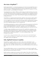
1
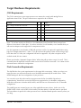
Danville Signal Processing, Inc. dspFlash™ Deluxe SHARC/Blackfin Flash Programmer User Manual Version 2.6 Danville Signal Processing, Inc. dspFlash™ User Manual Copyright © 2009-2014 Danville Signal Processing, Inc. All rights reserved. Printed in the USA. Under the copyright laws, this manual may not be reproduced in any form without prior written permission from Danville Signal Processing, Inc. Danville Signal Processing, Inc. strives to deliver the best product to our customers. As part of this goal, we are constantly trying to improve our products. Danville Signal Processing, Inc., therefore, reserves the right to make changes to product specification or documentation without prior notice. Updated operating manuals and product specification sheets are available at our website for downloading. This manual may contain errors, omissions or “typo’s”. Please send your comments, suggestions and corrections to: Danville Signal Processing, Inc. 38570 100th Avenue Cannon Falls, MN 55009-5534 Trademark Notice dspFlash is a trademark of Danville Signal Processing, Inc. VisualDSP++, CrossCore Embedded Studio, Blackfin, and SHARC are trademarks of Analog Devices, Inc. Windows, Windows XP, Windows 7 and Windows 8 are trademarks of Microsoft Corporation. Contact Information Danville Signal Processing, Inc. 38570 100th Avenue Cannon Falls, MN 55009 E-mail: Web Site: [email protected] http://www.danvillesignal.com Voice: 507-263-5854 Fax: 877-230-5629 dspFlash™ User Manual Page 2 Table of Contents Overview of dspFlashTM ............................................................................................ 5 Early dspFlash Versions & Updates ............................................................................ 5 Flash Devices ............................................................................................................ 6 Getting Started.......................................................................................................... 7 First Steps - Installation ............................................................................................. 7 Target Hardware Requirements ................................................................................ 8 JTAG Requirements................................................................................................................................... 8 Flash Connection Requirements ................................................................................................................ 8 Operation - Connecting to the dspFlash .................................................................... 9 For Version 2.0 and Later .......................................................................................................................... 9 Setting Up Your Target .............................................................................................................................. 9 Choosing and Uploading a file .................................................................................................................. 9 Writing a File .......................................................................................................................................... 10 Programming the Flash............................................................................................................................ 11 Manual Memory Operations ................................................................................... 12 Erase Chip............................................................................................................................................... 12 Erase Sector ............................................................................................................................................ 12 Pre-Program Test & Post-Program Test .................................................................................................... 12 Manual Write Operations ....................................................................................................................... 12 Manual Read Operations ........................................................................................................................ 12 Programmer............................................................................................................ 13 JTAG Chaining ........................................................................................................................................ 13 Advanced ............................................................................................................................................... 13 Tools ...................................................................................................................... 14 Upgrading Firmware ............................................................................................................................... 14 SDRAM Test ........................................................................................................................................... 14 Demo Mode ........................................................................................................................................... 14 Import New Chip Driver ......................................................................................................................... 14 Update Flash Library ............................................................................................................................... 14 Pre Programming and Post Programming Tests ........................................................ 15 Setup Testing .......................................................................................................................................... 15 The Scripting Commands ........................................................................................................................ 16 Testing SHARC DSPs ............................................................................................................................... 17 Testing Blackfin DSPs .............................................................................................................................. 17 Danville Signal JTAG Adapters................................................................................. 18 dspFlash™ User Manual Page 3 Troubleshooting and FAQs...................................................................................... 19 RoHS Compliance .................................................................................................. 20 Product Warranty ................................................................................................... 20 dspFlash™ User Manual Page 4 Overview of dspFlashTM Danville Signal's dspFlash™ is an onboard programming tool for both serial and parallel flash memory. These flash devices are programmed through a JTAG interface, using proprietary JTAG commands similar to an emulator. This programming method uses the target processor to program its own flash rather than relying very slow boundary scan commands. The dspFlash Deluxe has 128Mb of SDRAM to hold the file(s) to be loaded into flash, and a separate 128 Mb SDRAM to hold an image of a test function. The SDRAM needs to be uploaded to only once per session. The JTAG interface of the dspFlash programming module is hot swappable which allows for quick transition from board to board. These two features can greatly reduce programming time during production runs. The dspFlash uses a supporting stand-alone Windows application. This program is regularly updated and may be downloaded from the Danville Signal website. The Windows application provides an easy-to-use graphical environment aimed at quick and simple production programming. The program also embeds all the device drivers, which allows for new devices to be added quickly. Should the need arise; the dspFlash programmer can even reprogram itself. The dspFlash programming process requires very little knowledge of the target processor and basically reduces the flash programming process to the push of a button. The most demanding tasks to program a flash during production are reduced to: opening a previously saved configuration file, plugging a JTAG cable in properly, and possibly resetting the target processor in the event of an error. To actually configure the dspFlash you need to know the SPI or parallel flash configuration on the target board. This includes the Chip Select configuration, target processor, and target flash models. The dspFlash Windows application cannot generate a LDR or binary file directly, but uses LDR or binary files that are created using VisualDSP++ or CrossCore Embedded Studio or other development environments. If you do not have a background with these skills, you may want to check out the Danville Signal website, as well as the Analog Devices website for links to useful references. Danville engineers are also available to discuss your application. Early dspFlash Versions & Updates The dspFlash was originally available in two versions, a Basic version and the Deluxe version. The Basic version has been discontinued for many years. There were two hardware variants of the Basic version (1 & 2). All Deluxe versions are type 2. You can identify the Basic version from the Deluxe by the color of the LEDs;. the Deluxe version uses red LEDs and the Basic version used Green LEDs. The latest dspFlash hardware now uses a new internal flash and is not backwards compatible with versions before 2.60. We suffer from same problem as everyone else, we couldn't support a flash that didn't exist when the earlier firmware was written. Danville continues to support previous customers with free updates. These will work with the latest software. The new firmware automatically compensates for the various hardware variants. If you have dspFlash™ User Manual Page 5 a Version 1 dspFlash, please contact us before you attempt an upgrade. The pre and post test functions are not supported with the Basic version. Occasionally, the dspFlash firmware update with an older dspFlash (before 2.60) will fail. The update utility is built into the dspFlash Windows program. There is a plan B, the firmware can be rewritten via its JTAG connector, just like your target boards. We recommend that you have an ADI ICE or another dspFlash programmer available before you update an earlier version to insure that you do not disrupt your production line if the update should fail. The latest internal dspFlash update (version 2.60 or greater) is much more robust, but this not going to help until this firmware is loaded permanently into the dspFlash programmer. Flash Devices There are many different choices of flash memory devices that you can choose from when designing or updating your product. This plethora of choices makes it impossible to test or support every possible combination. We try to support and test many different configurations. The support list is maintained on our web site. Here are some recommendations: • • • • • • • If Danville uses a specific flash - DSP combination on our boards , it will always be supported. If ADI uses a flash - DSP combination on an EZ-Kit, it is probably tested and supported. AVOID PARALLEL FLASH. SPI flash have gotten much faster and larger and are much easier to layout. In most cases, you will want to use an SO-8 or SOL-8 package. The PCB footprint can be made universal. It is unlikely that we will add new support for new parallel flash devices. We generally have support for Adesto (Atmel), Micron (ST) & Spansion SPI devices. If a device is not on the list, it may still work with a driver for a similar part. In the future, we plan to have a set of CFI compliant drivers for serial flash. This will make long term support much easier since the flash will be able to tell the driver its requirements. If you are trying to program a parallel flash for an ADSP-21262 or ADSP-21364, you are likely to have a serious problem. These parts were designed before CFI compliant parallel flash. You cannot program a CFI compliant parallel flash with these DSPs and at this time, virtually all parallel flash devices are CFI compliant. You are going to need to migrate your design to boot from serial flash, find a sufficient supply of obsolete flash devices, or migrate to a newer SHARC (ADSP-214xx preferred). Check with us if you are starting a new design. We might be able to suggest a good flash candidate. dspFlash™ User Manual Page 6 Getting Started The dspFlash includes the following items: Hardware: • • • • dspFlash Programmer USB Cable 2 dspFlash JTAG cables JTAG Signal Integrity Adapter Documents (CD): • • • This Manual Windows Application Installer USB Drivers We recommend that you have the following tools: • • • Analog Devices VisualDSP++ or CrossCore Embedded Studio Analog Device HP USB, USB ICE, ICE-1000 or ICE-2000 Any necessary JTAG adapters You can purchase any of these tools from Danville Signal by visiting our website, where you can also find helpful links to other tools and documents. The dspFlash application program requires Windows XP, Windows 7 or Windows 8. You should have the latest service packs installed. First Steps - Installation Once you have received the dspFlash, the first thing to do is to plug it into the PC via the included USB cable. This will begin the driver installation process. Follow the Windows prompts and browse for the driver files on this CD located in the usbdrivers folder. Once the drivers are installed, please locate the msi file which will install the dspFlash programming application into your PC. The programming application should automatically detect the dspFlash programmer and connect to it and add it to the list of available dspFlashes. Connecting to the target is as simple as plugging in the JTAG cable. The target device can be either powered or unpowered when the cable is plugged in. Once your target is powered, the LED indicating the logic voltage level should light. If this does not light, you should refer to Analog Devices application note EE-68 which describes the proper JTAG connections, specifically pulling pin 5 high via a pull-up resistor. If this resistor is not present the voltage level of the target is assumed to be 3.3V. Configurations using lower logic level voltages without this pull-up resistor are not supported by the dspFlash. dspFlash™ User Manual Page 7 Target Hardware Requirements JTAG Requirements The JTAG connections to your target processor are assumed to comply with Analog Devices Application Note EE-68. The pin connections are required to be as follows. Ground 1 2 EMU Key, This pin should be removed 3 4 Ground Pulled to Vddio through a 4.7KΩ resistor1 5 6 TMS Ground1 7 8 TCK Ground1 9 10 TRST Ground1 11 12 TDI Ground 13 14 TDO Note 1: If you have wired your JTAG for a “Local Boundary Scan Controller” then you may have different connections for these pins. If you have wired for a local boundary scan controller then you will need an adapter on the target side to compensate for this. It is also important to note that the 4.7KΩ pull up resistor on Pin 5 is required for applications using logic level voltages other than 3.3 Volts. If you do not have this pull-up resistor and are using a logic level other than 3.3 Volts your configuration will not be supported. Any other exception can be worked around, this one cannot. Please note that the “Automatic Program Write” utilizes the pull-up resistor on pin 5 as well. This is essentially how the dspFlash can detect when a new device has been connected. You cannot use the Autostart feature without this configuration. Flash Connection Requirements The dspFlash also has certain requirements for the target flash connections. When you select your target processor you will notice that the rest of the blanks automatically fill in with values. These default settings are the boot configuration of your processor. You can select your chip select and for most processors the list of available chip selects is comprehensive, however the rest of the SPI lines are required to be in a bootable configuration. What this really means is that the MOSI, MISO, and SCK lines are all assumed to be in a bootable configuration. The parallel ports are assumed to use one of the applicable memory selects. In the case of the SHARC ADSP-21262 or the ADSP-21364 families, the base address of the flash must be specified. The base address is specified for other processors but is calculated based upon the memory select you are using. dspFlash™ User Manual Page 8 Operation - Connecting to the dspFlash For Version 2.0 and Later Your dspFlash should be automatically detected when it is plugged into the computer and added to the list of available dspFlashes upon its enumeration. Setting Up Your Target Setting up a connection on the dspFlash is simple. Step 1: Select the target processor. To do this, select the processor on the target board from the pull down box. Step 2: Select your flash configuration, at the current time both SPI and parallel flashes are supported. If you are using a SPI flash the next step is to specify your chip select line by choosing it from the CS pull-down box. If you are using a parallel flash you have to specify either the memory select line that the flash is connected to or the base address. The base address is user supplied for the ADSP-21262, and ADSP-21364 families and is used to signal the location of the flash to both the dspFlash programming module and to the target. Step 3: Select the manufacturer of the target flash to be programmed, then the model of the flash. You no longer need to select the type of ldr file you are using because it is automatically detected. Many file types can be written to flash. If you are writing any sort of file that does not conform to ADI ldr file formats (ASCII, or Intel Hex) will be written as a binary file. If you are programming an audio file, a video file, or a binary loader file they will be written bit for bit as they are in the files. Choosing and Uploading a file With the dspFlash you can write many types of files into flash including LDR files which can be used to boot the processor. There are specific configurations you must adhere to write bootable code to the flash. For example, if you are using a Blackfin BF-532 and a SPI flash, you have to have a CS of PF2, and write with an offset of zero. Bootable code must be written with an offset address of zero. If you are using a SPI flash and a SHARC processor, you also must bit reverse your data file. This is required because of differences in the booting SPI configuration and normal SPI configurations. This bit reversing can be done by checking the Bit box next to the applicable file(s). If you have already uploaded your code and must change this setting, it is necessary to upload the file again. It is important to note that when you are working with multiple files you do not have to bit reverse every file you are working with. If you would like to bit reverse every file you are going to write you have to check every bit reverse box. If your file is not intended to boot your processor your options are much more flexible. There are dspFlash™ User Manual Page 9 many more chip select lines to choose from, and you can make use of loading with offsets. These files should be written in binary format and will be imaged bit for bit into flash. Once you have chosen your data file and bit reversed it if need be, the next step is to upload. Uploading your data file to the dspFlash programmer will send the configuration, processor, and flash to the dspFlash. This is important because if any of these things are changed, uploading will need to be repeated. Once your file has been uploaded then you are ready to perform flash operations. Writing a File There are three options to consider when writing a file to flash. The first of these is the offset address. This will dictate to the dspFlash where to start the file writing process. This address will need to be zero for booting cases, and can be nonzero for non-booting applications. The average write speed of the dspFlash is 33kB/s; this may vary depending on your processor and flash. The second option to consider while writing files to flash is the preprogram erase operation. This operation has three possible settings: erase affected, erase all, and no erase. If you choose to erase affected it will only erase the sectors that will be affected by the writing operation. If you choose erase all, the entire chip will be erased prior to writing, and if you choose no erase, no erase will take place prior to the writing. Due to the huge erase times of large flashes, which can take minutes, erase affected can often be more efficient. If your file is large enough to occupy 85-90% of the flash you are using, then erase all may be a better option. If the flash on your target board is blank then no erase is definitely the best option, because it adds no extra time to your operation. The third option you have is whether or not you would like to use any of the new automatic programming additions. These automatic programming features allow the user to program strings, date stamps, or serial numbers to the flash immediately after programming completes. These features can be setup by choosing “Setup Auto.” This will bring up the following dialog (graphic shown on next page). From this dialog you can specify a starting serial number, a starting address for one of two automatic programming options, and whether you would like your serial number programmed as part of an ASCII string or as a binary number. You can also choose whether or not to erase the affected sector(s). You can embed the selected date with the “@” symbol, or the serial number with the “$” symbol. dspFlash™ User Manual Page 10 During a production run, the program button can be the only button to click to trigger the programming of another board, assuming the target board is the same as the previous board. This can save valuable time during a long production run. If you have the pull up resistor on pin 5 of JTAG, then you can save even more time by clicking the Start Automatic Program Write button and then when a new device is detected the write file programming sequence will be triggered. This can save a significant amount of time and can keep an operator from making unnecessary repetitive motions to click a button over and over again. Programming the Flash To write your file(s) to flash you simply have to click the Program button next to the dspFlash you wish to write from. This will initialize the writing process and you can monitor the progress of each dspFlash with the individual progress bars. dspFlash™ User Manual Page 11 Manual Memory Operations Erase Chip If you choose the Erase chip operation your entire flash will be erased. It is important to note that this operation can take over a minute for larger flashes. Once this process has been initiated it cannot be stopped as well, so if you are using a big flash and click it you are in for the wait. Erase Sector Choosing Erase Sector will erase the sector that contains the address in the address box. Sectors can vary in size and the dspFlash will erase the largest possible sector for the address you have selected. If you need to know the size of the sector that will be erased you can view it from the memory section of the datasheet of your flash. Pre-Program Test & Post-Program Test Clicking this button will execute the script that corresponds to the test you click. These scripts are specified in the test setup dialog, which can be accessed by clicking Setup Test from the main dialog. This will execute the script the same way it would be executed during the production process. Manual Write Operations The auxiliary write operation can be used for many things. You can write individual values or you may write ASCII strings. For example, you could use it to write copyright notices into flash using the write string operation. You could also use it to write a serial number or calibration values. In order to write values, you have to specify three things: 1) The starting address in flash where the writing begins. 2) Select the size of the word (8, 16 or 32 bits). 3) Specify the data to be written. This data is specified in hexadecimal characters. Strings are written in a similar fashion. You specify the starting address and string radio button. The string can be up to 64 characters long. It is automatically terminated with a null character (0x00). Manual Read Operations There are four options for auxiliary read operations, which can be used to read the contents of your flash. You can read one, two, or four bytes, or you can read an ASCII string. The difference here is that if you read an ASCII string the values will be decoded and the read will stop at the terminating null character, or if this character is not found, a read of 64 characters will be performed. The read operation is performed as follows; first specify the starting address in the start address box, second select the read you want, and then perform the read. dspFlash™ User Manual Page 12 Programmer JTAG Chaining Please note: Only JTAG devices with 5 bit instruction registers are currently supported; this includes all ADI Sharcs, Blackfins, and TigerSharcs. JTAG chaining gives a hardware designer the ability to control multiple JTAG devices through a single JTAG connector on the board. The implementation of JTAG chaining is presumed to comply with both Analog Devices application note EE-68 and the IEEE 1149.1 JTAG boundary scan standard. When you enable JTAG chaining two boxes will appear next to your select processor box. These boxes are JTAG chain length, and JTAG chain position. The JTAG chain length counts from one and represents the number of JTAG devices in the scan chain. The other box is the JTAG chain position. The device, which is connected to the TDO of the JTAG connector, is device zero. The device, which is connected to TDI of device zero, is device one. If you follow this chain you should be able to determine which device is which. If you have four devices in you JTAG scan chain then the last device in your scan chain is device three. Advanced Core Clock Modification This feature will not be available upon initial release but will be implemented on future releases. To increase core clock speed, you can adjust the core clock registers from the advanced menu. Note: This procedure should be done with caution. Improper settings in the core registers can cause the target DSP to meltdown. If you know the values you would like to write to the registers, you can uncheck the use default values box, and then input the applicable values for the registers for your processor. Since these values are dependent on the oscillator you are using, predefined register values will be an unlikely upgrade in the future. Connection Register Modification Possibly the best way to improve performance is to adjust the values written to the connection registers, either the SPI or parallel controls. In order to change these register values, you have to click the use default values checkbox, which will allow editing of the registers. The values you choose will be used in place of the default register values we used for testing at Danville Signal. These values generally use a 10MHz SPI clock frequency, or a medium number of wait states on a parallel connection. This was written to try to compromise widespread device support with the same values while still maintaining an acceptable level of performance. Please refer to your target processors hardware reference manual available from Analog Devices for register definitions. dspFlash™ User Manual Page 13 Tools Upgrading Firmware With every application update there may be a firmware upgrade. The process of upgrading the firmware of the dspFlash is simple; just click the Upgrade Firmware button on the Tools Menu. You will be asked to confirm firmware upgrade, after it is completed, you will need to restart both the application and the dspFlash programming module. When you restart the application you should see your new firmware revision in the message center. SDRAM Test Testing the SDRAM of your dspFlash programming module may occasionally be necessary. It would also be recommended if you start to see problems across multiple boards. To execute the test click the SDRAM test under the tools menu. If there is a hardware problem, please call or e-mail Danville Signal’s support department to discuss options. Demo Mode This feature is designed to allow anyone to take a test drive of the dspFlash. It creates four “Demo” units that can be used just like dspFlash units, so you can get the hang of using the dspFlash application or create your configuration files without the presence of the dspFlash. These virtual dspFlash units will allow you to test and debug files and works similarly to the dspFlash. Import New Chip Driver This option will allow you to add support for new DSPs and even more flashes if new internal drivers are needed. Once you have chosen this you will see a file dialog where you can specify your new chip driver. The new chip drivers are available for download individually from www.danvillesignal.com/support. Update Flash Library This option allows you to update the flash library that may or may not need to update the chip drivers as well. Once this option is chosen you will see a file dialog where you can select the new flash library. The new flash libraries are available for download from www.danvillesignal.com/support. dspFlash™ User Manual Page 14 Pre Programming and Post Programming Tests The deluxe version of the dspFlash supports running test programs either before or after programming the flash. These programs are specified in ldr file format. This allows you to do things like check the SDRAM on your board, or ring out a Codec, or even test the I/O by blinking lights on a test module and interacting with the user. The flow of the test program works like this. Start C Script OK/Bad What is the result? OK Program C Script DSP Test Program OK/Bad Stop DSP Test Program Bad The dspFlash executes the test program based on a C script. This script allows the user to interact with R0-R7 on the target DSP which makes it possible to setup your program to use a jump table and execute multiple tests sequentially and conditionally based on the results of the previous tests. Setup Testing The test options are accessed through the Setup Testing dialog. dspFlash™ User Manual Page 15 The first thing to do when configuring your test is to specify your test ldr file. This is done by clicking the “…” which will bring up a file dialog where you can select your test file. You can specify both pre-program and post-program tests from this dialog and then you can enable them from the main screen. The Scripting Commands Like all C programs, the C program starts with main(). The dspFlash main is of type bool and will return either true or false which correspond to pass and fail. There are several supported functions with their standard C support. If/else – the conditional operators Ex If(r0 == 6 && r1 == 2) { function1(); } else function2(); askif/else – conditional operation based on message box which poses the question to the operator dspFlash™ User Manual Page 16 Ex askif(“Question”) function1(); else function2(); message – reports a string to the message box. Ex Message(“R0 = “+r0); for – loops for a specific user count Ex for(int I = 0; I < 10; I++) { Do something… } test – executes the tests program Ex R0 = 1; test(); if (r0 == 2) return true; else return false; while – execute while condition is true Ex while( r0 !=2) { function(); test(); } Testing SHARC DSPs A example for testing SHARC DSPs is provided with the CD. We used the Danville Signal dspblok 21469 as the test case to illustrate how users can incorporate testing using the dspFlash. The folder SHARC_test_example contains a Visual DSP project, a compiled ldr file, a test script and dspFlash programming file that utilizes the testing mechanism. Please read through some of the text files that serve as documentation for this example. Testing Blackfin DSPs Blackfin testing is in alpha stage. The mechanisms are intact but the support team has not yet provided a working example to properly ring out this feature. Danville will update its website as soon as an example is provided. You are welcome to try using test scripts with Blackfins, but we are making no promises. We decided to include this feature since many of our users are early adopters and might want to give it a try. dspFlash™ User Manual Page 17 Danville Signal JTAG Adapters You may notice that the Danville Signal JTAG adapter is available for purchase along with your dspFlash programmer. On our boards we use a male 16 pin, 2mm dual row header as our JTAG connection. This is smaller than the connectors used by Analog Devices. We offer an adapter to convert this 2mm header to the standard 0.100 headers used by the Analog Devices emulators as well as the dspFlash JTAG connection. If you want to use the Danville JTAG adapter, the connections are exactly the same as the larger ADI connector with the exception of Pins 15 & 16. These pins do not exist on the ADI JTAG connector and are tied to Vd+3.3 (IO Voltage) on Danville boards. dspFlash™ User Manual Page 18 Troubleshooting and FAQs When programming flash a number of problems can occur. A brief discussion of common problems can be found below. If you have a problem not listed here feel free to contact Danville Signal at [email protected]. Problem: I can’t seem to connect to the dspFlash programming module Solution: First try power cycling the dspFlash, simply unplug and plug it in again. Restart the application and see if that solves the problem. If not, is the status light illuminated on the dspFlash? If the status light is not illuminated, there is possibly a problem with the driver. Reinstall the driver provided on the CD. If it still doesn’t work, contact Danville Signal. Problem: I wrote a working LDR file to a target but it doesn’t boot properly Solution: The most likely cause of this is writing the file improperly. If you are using a processor with an SPI flash then bit reversing is necessary. The other possible programming problem would be if the file were written with an offset. Writing with offset is not a bootable configuration. The other cause of this could be hardware. If your hardware is not configured properly booting will not take place. Most processors have specific requirements regarding which chip selects can be used, and how the flash is connected. In a parallel setup a certain memory select must be used. Problem: I wrote something to the flash and now I can’t connect to my target, even with an emulator Solution: This probably happened because what was written to flash caused a processor core fault which results from bad code in the boot area of the flash. This can be remedied by changing the boot configuration pins of your processor. If these pins are tied directly to a supply and not through a pullup or pull-down resistor, then this method probably will not be possible. This can also be remedied with an emulator and exceptional timing. The trick to fixing the problem this way is to connect to your device between power-up and boot. This is possible on most processors, however can be quite tricky. Once the processor is booted and not faulted you should be able to erase the flash either with the emulator or with the dspFlash. If you are going to switch from the emulator to the dspFlash, you should be careful not to power cycle or reset the device or you will have to start the process over again. If neither of the other options worked it may be necessary to remove the flash and erase it by some other method. dspFlash™ User Manual Page 19 RoHS Compliance The European Union approved a directive on the restriction of the use of certain hazardous substances in electrical and electronic equipment. This directive is commonly known as RoHS, EU Directive 2002/95/EC. This directive severely limits the amount of lead and 5 other substances that can be in contained in nonexempt products. The directive became European law in February 2003 and took effect July 1, 2006. The dspFlash is RoHS compliant. Product Warranty Danville Signal Processing, Inc. products carry the following warranty: Danville Signal Processing products are warranted against defects in materials and workmanship. If Danville Signal Processing receives notice of such defects during the warranty period, Danville Signal Processing shall, at its option, either repair or replace hardware products which prove to be defective. Danville Signal Processing software and firmware products which are designated by Danville Signal Processing for use with our hardware products are warranted not to fail to execute their programming instructions due to defects in materials and workmanship. If Danville Signal Processing receives notice of such defects during the warranty period, Danville Signal Processing shall, at its option, either repair or replace software media or firmware which do not execute their programming instructions due to such defects. Danville Signal Processing does not warrant that operation of the software, firmware, or hardware shall be uninterrupted or error free. The warranty period for each product is one year from date of installation. Limitation of Warranty: The forgoing warranty shall not apply to defects resulting from: • • • • • Improper or inadequate maintenance by the Buyer; Buyer-supplied software or interfacing; Unauthorized modification or misuse; Operation outside the environmental specification of the product; Improper site preparation and maintenance. Exclusive Remedies: The remedies provided herein are the Buyer’s sole and exclusive remedies. In no event shall Danville Signal Processing, Inc. be liable for direct, indirect, special, incidental or consequential damages (including loss of profits) whether based on contract, tort, or any other legal theory. dspFlash™ User Manual Page 20