1
US008255587B2
(12) Ulllted States Patent
(10) Patent N0.:
McClure et a].
(54)
US 8,255,587 B2
(45) Date of Patent:
PROTOCOL ADAPTER FOR PASSING
(52)
*Aug. 28, 2012
US. Cl. .............. .. 710/16; 710/73; 710/74; 701/24;
DIAGNOSTIC MESSAGES BETWEEN A HOST
701/29; 701/31; 701/33; 701/33; 701/36;
COMPUTER AND VEHICLE NETWORKS
701/53
OPERATING IN J 1939 OR ‘H708 PROTOCOL
(75)
(58)
F1010 01 00331110011011 Search ................ .. 340/431,
Inventors: Robert E. McClure, Danville, IN (US);
_
David M_ such’ Greenwood’ IN (Us)
(73) Assignee: Dearborn Group, Inc., Farmington
Hills, MI (US)
(*)
Notice:
(56)
_
_
_
_
References Cited
5,491,418
Th1s patent 1s subject to a termmal d1sclaimer.
A
5,541,840 A
5,555,498 A
(21) Appl. N0.: 13/199,340
Filed,
Aug 26 2011
.
.
2/1996
A11310 et 31.
................ .. 324/402
7/1996 Gume etal.
9/1996 Berra et al.
5,646,865 A
7/1997 Alfaro et al.
2/1999 1011118011
5,964,852 A
,
*
5,870,573 A
5,896,569 A
(22)
340/933;_ 710/72T74
US. PATENT DOCUMENTS
4,602,127 A
7/19g6 Neely et a1‘
4,975,846 A
12/1990 Abe et a1.
5,077,670 A
12/1991 Takai et 31.
Subject to any disclaimer, the term of this
patent is extended or adjusted under 35
U.S.C. 154(b) by 0 days.
_
_
See appl1cat1on ?le for complete search h1story.
4/1999 Butler et al.
10/1999 Overton
(Continued)
(65)
Prior Publication Data
Us 2011/0314191 A1
Dec. 22, 2011
_
OTHER PUBLICATIONS
_
Dearborn Group, Inc., Dearborn Group Technology, 11850 Network
Related U‘s‘ Apphcatlon Data
(60)
Analysis Tool, 1NAT User’s Manual Version 5.0, 1999, 63 pages,
Continuation of application No. 12/799,739, ?led on
Apr. 30, 2010, noW Pat. No. 8,032,668, Which is a
_
P1’lmary Examme" * Tammara Peyton
Dec. 17, 2007, noW Pat. No. 7,725,630, Which is a
division ofapplication No. 10/888,432, ?led on Jul. 9,
(74) Attorney, Agent, or Firm *Warn Partners, P.C.
2004,
(51)
_
continuation of application No. 12/002,427, ?led on
noW
Pat.
No.
7,337,245,
Which is
a
connnuanon'm'pan of apphcanon NO‘ 09/532’718’
(60)
Farmington Hills, Michigan
(57)
ABSTRACT
A protocol adapter for transferring diagnostic messages
?led on Mar‘ 22’ 2000’ HOW Pat‘ NO‘ 6’772’248'
betWeen netWorks Within a vehicle and a host computer. The
Provisional application No. 60/126,588, ?led on Mar.
protocol adapter operates as a voltage translator to support
26, 1999,
11708 software. The protocol adapter also recognizes When
the protocol adapter is connected to a host computer running
the 11939 and/or 11708 protocols and automatically sWitches
to that protocol.
Int. C1.
G06F 13/12
G06F 3/00
G06F 15/173
(2006.01)
(2006.01)
(2006.01)
16 Claims, 9 Drawing Sheets
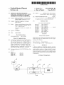
18
K
K 10
STORAGE
K74 16
HOST
COMPUTER
V 12
——-l
l
I/O BUARD—_Il
CPU BOARD
L 34
[I
IN- VEHICLE
NETWORKS
US 8,255,587 B2
Page 2
US. PATENT DOCUMENTS
6,122,684 A
9/2000 Sakura
6,181,992 B1
6,189,057 B1
1/2001 Gurne et a1.
2/2001 SchWanZ
etal.
.
6,193,359 B1
6,195,359 B1
2/2001 Pam 6‘ a1~
2/2001 Eng etal.
6,321,151 B1
6,526,340 B1*
11/2001
ShultZ
2/2003 Reuletal. ..................... .. 701/29
6,571,136 B1
6,608,554 B2
5/2003 Staiger
*
6,772,248 B1
7,337,245 B2
7,725,630 B2
7817019 B2*
’
’
_
_
* clted by examlner
8/2003 Leseskyetal. ............. .. 340/431
8/2004 McClure et :11.
2/2008 McClure et :11.
5/2010 McClure et :11.
10/2010 Lesesky ...................... .. 340/431
US. Patent
Aug. 28, 2012
Sheet 1 of9
US 8,255,587 B2
35_.: 33%_
N)J
Q
\a.
R
a
“a
5%EM"
2AM'
E28
/
at
_-
Go:
muéEm
US. Patent
Aug. 28, 2012
Sheet 2 of9
US 8,255,587 B2
nrq
90010
N
at
592 58%
e2 SE M.Em
US. Patent
Aug. 28, 2012
Sheet 3 of9
a:g:
US 8,255,587 B2
.5NE
- gm
- $5
ANN-{II
mat
82AU
~|Hvswe
Hvea.
US. Patent
Aug. 28, 2012
Sheet 4 of9
AU
Lmw v. AU
A
AEm a
3%
US 8,255,587 B2
25%:
HH
II11
at
Q-
FvTUL
m‘5.:E
H4.
AU
$2
,.a:
A,
13%
m 55mm5=22aws11:
ax:n5
55%
5H
§§
Au
@856
US. Patent
Aug. 28, 2012
Sheet 6 of9
US 8,255,587 B2
[5%
a?
Em a
US. Patent
$3
Aug. 28, 2012
Sheet 7 of9
US 8,255,587 B2
0
2
E
Sq
u
“5
3.5 Iv$3=2
s5
22am“
E‘Iv2
3%
a
.
m
2QM
=2
ll
52%AU
US. Patent
Aug. 28, 2012
Sheet 9 of9
US 8,255,587 B2
anI.2“
EN
3M1 2.>2iv
>5alv
an2s:
RE
55
3
=
aam ?s 23%N9 a,a“
a.
G
a
a
EE5Nm
a
E3
m
2%
E:g
22
3Q8QL.W“SE
EsE
N“:
Os“
- Em
R
h
<
“
n.
a“
M
m
585%
“
s
U
Q
v
\
m
2e:.I
Lw
\w5.Esfuq
U
mm‘.
US 8,255,587 B2
1
2
PROTOCOL ADAPTER FOR PASSING
DIAGNOSTIC MESSAGES BETWEEN A HOST
COMPUTER AND VEHICLE NETWORKS
OPERATING IN J1939 OR J1708 PROTOCOL
to detect the end of message, but also added an inherent delay
betWeen the vehicle data link and the ho st computer serial
communication port.
The J1939 protocol required that softWare had to be
matched to the diagnostic tool for Which it Was Written. Obso
lete softWare had to be paired With legacy hardWare, and neW
softWare had to be paired With neW hardWare. This required
CROSS-REFERENCE TO RELATED
APPLICATIONS
that each diagnostic shop oWn and maintain several diagnos
This application is a Continuation Application of US. Ser.
No. 12/799,739 ?ledApr. 30, 2010, Which is a continuation of
US. Ser. No. 12/002,427 ?led Dec. 17, 2007, Which is a
10
tic tools. It Would be desirable to have a protocol adapter that
could operate as an old voltage translator to support obsolete
softWare using the J1708 protocol, and recogniZe When the
Divisional Application of US. application Ser. No. 10/888,
432, ?led Jul. 9, 2004, Which is a Continuation-in-Part Appli
cation ofU.S. application Ser. No. 09/532,718, ?led Mar. 22,
protocol adapter is connected to a host computer running neW
softWare to automatically sWitch to the J1939 protocol.
2000, Which claims the bene?t of US. Provisional Patent
SUMMARY OF THE INVENTION
Application Ser. No. 60/126,588, ?led Mar. 26, 1999.
In accordance With the teachings of the present invention,
a protocol adapter is disclosed for transferring diagnostic
BACKGROUND OF THE INVENTION
20
support J1708 softWare. The protocol adapter also recogniZes
This invention relates generally to a protocol adapter for
passing diagnostic messages betWeen netWorks Within a
vehicle and a host computer and, more particularly, to a
protocol adapter for passing diagnostic messages betWeen
25
netWorks Within a vehicle and a host computer, Where the
protocol adapter includes a pass-through mode of operation
Where the protocol adapter emulates legacy protocol adapters
so that state of the art host computers can communicate With
the vehicle netWorks using obsolete softWare.
messages betWeen netWorks Within a vehicle and a host com
puter. The protocol adapter operates as a voltage translator to
1. Field of the Invention
30
2. Discussion of the RelatedArt
Vehicles employ various netWorks and systems for diag
nostics, analysis and monitoring of vehicle systems. These
When the protocol adapter is connected to a host computer
running the J1939 and/ or J1708 protocols and automatically
sWitches to that protocol.
In one embodiment, the protocol adapter includes a control
area netWork (CAN) transceiver circuit that provides an inter
face betWeen the vehicle netWork and the host computer When
the vehicle netWork is operating in a J 1939 protocol and a
J1708 transceiver that provides an interface betWeen the
vehicle netWork and the host computer When the vehicle
netWork is operating in a J1708 protocol. The J1708 trans
ceiver circuit includes a voltage translator for translating the
voltage of the J1708 protocol signals. The protocol adapter
various netWorks are generally selectively connectable to an
external host computer so that the operation of the vehicle
netWorks can be monitored by an external system. These
further includes a static random access memory (RAM) cir
cuit that provides temporary data storage and is connected to
the CPU through data and address channels, a ?ash memory
vehicle systems and netWorks operate under various proto
cols, such as the J1708 and the J1939 protocols. Protocol
module that provides permanent storage of application data
and loader application information, and a universal asynchro
adapters are knoWn in the art that alloW the host computer to
nous receive and transmit (UART) circuit that provides com
munication of asynchronous data to and from the host com
communicate With the vehicle netWorks through the proto
cols.
puter.
One knoWn type of protocol adapter for this purpose is the
J1708 protocol adapter. The ?rst generation of the J1708
protocol adapterused for diagnostic purposes included a volt
Additional advantages and features of the present inven
tion Will become apparent from the folloWing description and
appended claims, taken in conjunction With the accompany
age translator With a built-in-timer circuit that ?agged the end
ing draWings.
of a message. This protocol adapter design Worked Well for
J 1708 protocols because it and the standard serial communi
BRIEF DESCRIPTION OF THE DRAWINGS
cation port of the host computer Were based on universal
asynchronous receive and transmit (UART) technology hav
ing different physical interfaces, i.e., different voltages. The
FIG. 1 is a block diagram of a protocol adapter system,
according to an embodiment of the present invention, that
timer circuit Was needed to alloW the host computer to rec
transfers both J1708 and J1939 signals betWeen a host com
ogniZe the end of message as de?ned by the J1708 protocol.
Most host computers, hoWever, did not have adequate
resources to comply With the rigid timing requirements
needed for end of message detection.
puter and a vehicle netWork;
FIG. 2 is a schematic block diagram of an input/output
A second generation protocol for vehicle diagnostics pur
in the I/O board shoWn in FIG. 2;
FIG. 4 is a schematic diagram of a poWer supply regulator
circuit in the I/O board shoWn in FIG. 2;
(I/O) board in the protocol adapter shoWn in FIG. 1;
FIG. 3 is a schematic diagram of a J1708 transceiver circuit
poses is the J1939 protocol. With the J1939 protocol, there
Was no longer a basic compatibility betWeen the knoWn host
computer serial communication port and the J1939 protocol.
60
FIG. 5 is a schematic diagram of an LED indicator circuit
microprocessors in their diagnostic tools. These micropro
in the I/O board shoWn in FIG. 2;
FIG. 6 is a schematic block diagram of a central processing
cessors Would receive an entire message from one of the
unit (CPU) board in the protocol adapter shoWn in FIG. 1;
It therefore became necessary for protocol adapters to use
supported links, and do message validation, including end of
message detection. The microprocessor Would then forWard
the message on to the appropriate communication channel if
it did not detect an error. This alleviated the need for the timer
65
FIG. 7 is a schematic diagram of the central processing unit
in the CPU board shoWn in FIG. 6;
FIG. 8 is a schematic diagram of a static memory module
circuit in the CPU board shoWn in FIG. 6; and
US 8,255,587 B2
4
3
FIG. 9 is a schematic diagram of an I/O interface connector
circuit in the CPU board shown in FIG. 6.
-continued
WR*-active low signal used for external Writes
EXTINT-designates an external intenupt
AD[0.15]-address data lines to transfer between the processor
DETAILED DESCRIPTION OF THE
EMBODIMENTS
and memory
LA[0.15]-latch address used to latch the desired memory bytes
EPA3-input/output for high speed capture/compare channels
EPA8-input/output for high speed capture/compare channels
EPA9-input/output for high speed capture/compare channels
The following discussion of the embodiments of the inven
tion directed to a protocol adapter for transferring both 11708
and 11939 protocol diagnostic messages between networks
within a vehicle and a host computer is merely exemplary in
SCO-clock pin for SSIOO
SDO-data pin for SSIOO
SCI-clock pin for SSIOO
SDI-data pin for SSIOO
P2.4—standared bi-directional ports for data transfer
nature, and is in no way intended to limit the invention or its
applications or uses.
FIG. 1 is a block diagram of a system 10 for transferring
diagnostic signals between vehicle networks 12 in a vehicle to
an external host computer 14 through a protocol adapter 30.
Such diagnostic messages can be any signals for monitoring
any suitable vehicle network within the vehicle for diagnos
TXD-used to transmit serial data
RXD-used to receive serial data
TXCAN-used to transmit CAN signal
RXCAN-used to receive CAN signal
A[9.15]—high level address for selecting large byte operations
HDWfRST*-active love hardware reset
FLASHfUPPER-FLASH upper byte
FLASHfCS*-active low enable FLASH chip select
RAMfCS*-active low enable RAM chip select
20 UARTfCS*-active low enable UART chip select
D[0.15]-data signal used to transfer data bi-directionally between
including state of the art host computers and obsolete host
tics and/or maintenance purposes, as would be well under
stood to those skilled in the art. The host computer 14 can be
any host computer known in the art used for this purpose,
the processor and memory
computers. The host computer 14 includes an RS-232 I/O
port 1 6 that provides an RS —232 interface to the host computer
14. The RS-232 port 16 provides direct access to the 11708/
A[1.15]—address signal used to select the desired memory
allocation area
CE’ZLOWER-active low chip enable for lower byte
RS-485 link. The signals received and analyZed by the host 25 DE’ZLOWER-active low data enable for lower byte
WE’ZLOWER-active low write enable for lower byte
computer 14 can be stored in any suitable storage device 18,
CE’lUPPER-active low chip enable for upper byte
such as a display or magnetic tape. The signals used by the
DE’ZUPPER-active low data enable for upper byte
vehicle networks 12 can be of any particular vehicle protocol,
WE’lUPPER-active low write enable for upper byte
FLASHfUPPER-FLASH upper byte write enable
including the 11708 protocol provided on line 20 and the
30 FLASHfCE*-active low FLASH chip enable
11939 protocol provide on line 22.
FLASHiDE’g-active low FLASH data enable
FLASHfWE*-active low FLASH write enable
A[1.3]—address signal used to select the desired allocation area
According to the invention, the protocol adapter 30 is com
patible for both the 11708 protocol and the 11939 protocol.
The protocol adapter 30 provides a “pass-through” interface
so that various compliant applications from various develop
ers can use any of the unique developer applications. This
allows all compliant software applications and hardware
interface adapters to be interchangeable. The protocol adapter
30 is capable of performing electronic control module (ECM)
emulation, analysis of network message loading, simulation
of message traf?c loading of an in-vehicle network, inventory
management, ECM code testing, a gateway between net
works and vehicle maintenance status checks.
The protocol adapter 30 includes an I/O sub-assembly
board 32 and a CPU sub-assembly board 34, both of which
will be described in detail below. When the vehicle networks
12 use the 11708 protocol, the protocol adapter 30 can operate
in a pass-through mode where the 11708 signals on the line 20
are passed through a voltage translator directly to an RS-232
transceiver in the I/O board 32. With the 11708 protocol, the
protocol adapter 30 can also operate under the control of an
embedded processor where the 11708 signals on the line 20
are passed through a voltage translator to be processed in the
CPU board 34 and routed to an RS —232 transceiver (discussed
below) in the I/O board 32. If the vehicle networks 12 are
using the newer 11939 protocol, the 11939 signals on the line
22 are processed in the CPU board 34 to provide the 11939
D[0.7]—data signal used to transfer data bi-directionally between the
processor and memory
35 CS*-active low chip select
RESET-signal used for reset
INTR-interrupt line to processor
SOUT-data out
DTR* —active low enable data terminal ready
RTS*-active low enable ready to send
MBAUD-used to set the processor in high speed mode.
40
Unused in this application.
SIN-data in
DSR*-active low enable data set ready
CTS*-active low enable clear to send
EPA3-input/output for high speed for capture/compare channels
EPA8-input/output for high speed for capture/compare channels
45 EPA9-input/output for high speed for capture/compare channels
P2.4—PC LED control
UARTiSOUT-UART data out
UARTiDTR>g —active low enable UART data terminal ready
UARTfRTS*-active low enable UART ready to send
UARTiSIN-UART data in
50 UARTfDSR*-active low enable UART data set ready
UARTiCTS’g-active low enable UART clear to send
55
compatibility.
The U0 board 30 and the CPU board 34 use the following
list of signals:
60
ACH[2.7]-inputs for the analog/digital converter
RESET*-active low signal issued to reset the processor
READY-signal used to lengthen memory cycles for slow memory
RD*-active low signal used for external memory reads
WRH*-active low signal used to designate high-byte Writes
65
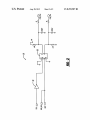
FIG. 2 is a schematic block diagram of the I/O board 32.
The (U0) board 32 includes an external I/O interface circuit
40, an RS-232 transceiver circuit 42, a power supply regulator
circuit 44, a controller area network (CAN) transceiver circuit
48 for the 11939 protocol, a 11708 transceiver circuit 50
including a voltage translator, an LED indicator circuit 52 and
input and output ports 54 and 56 interconnected as shown.
The external I/O interface circuit 40 provides the interface
connection between the various circuits in the I/O board 32
and the connections to the host computer 14 and the vehicle
networks 12. The RS-232 transceiver circuit 42 provides an
RS-232 interface between the vehicle networks 12 and the
host computer 14.
The CAN transceiver circuit 48 provides a CAN interface
between the vehicle networks 12 and the host computer 14
US 8,255,587 B2
5
6
When the vehicle networks 12 are operating in the J1939
protocol. In one embodiment, the CAN transceiver is the
model P82C25 1 T, Well knoWn to those skilled in the art. The
monitors the data so as to provide the J1708 de?ned timing
signals on any or all of the RS-232 hardWare handshake
J 1708 transceiver circuit 50 provides the J 1708 protocol
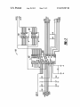
FIG. 8 is a schematic diagram of the static RAM circuit 92,
and includes a memory chip 110 andAND gates 112, 114 and
signals.
interface betWeen the vehicle netWorks 12 and the host com
puter 14. FIG. 3 is a schematic diagram of the J1708 trans
ceiver circuit 50 and includes a voltage translator 68 and an
input buffer 70 electrically interconnected, as shoWn. In one
116 electrically interconnected as shoWn. In one embodi
ment, the memory chip 110 is the model TC551664BJ-20,
Well knoWn to those skilled in the art. The memory chip 110
is used for temporary data storage and is connected to the
CPU 100 through the data and address channels. Once a
memory allocation area is speci?ed through the address chan
nel, data can be read or Written through the data channel. Data
embodiment, the voltage translator 68 is the model SN75176,
Well knoWn to those skilled in the art.
Both the transceiver circuits 48 and 50 include transmit
mailboxes for transmitting J1708 and J1939 messages to the
signals D(0-15) are used to transfer data bi-directionally
betWeen the CPU 100 and the memory chip 110. Address
signals A(1-15) are used to select the desired memory allo
cation area in the memory chip 110.
The static RAM circuit 92 provides space reserved in the
adapter’s memory for the temporary storage of data for the
transmit and receive mailboxes. The static RAM circuit 92
netWorks 12 and receive mailboxes for receiving J1708 and
J 1939 messages from the netWorks 12. The protocol adapter
30 alloWs the user to customiZe each transmitted message.
The J1708 or J1939 message to be transmitted may include
the relative time to the adapter timer, When the message
transmission is to begin, the number of times the message is
to be sent, the desired time interval betWeen transmissions,
20
announcing a successful transmission, the number of times
the message should be sent before auto-deletion occurs, and
Whether to enable a call back announcing the time of message
deletion. The J 1708 or J 1939 message received may include
mailbox data, storage for oversiZed messages, such as J1939
transport protocol messages, and the concatenation of small
25
Which protocol to scan, Which bits should be masked by
hardWare-level ?ltering, Which bits should be matched by
hardWare-level ?ltering, What information, such as mailbox
30
cation Will be noti?ed When a message is received, such as
transparent update, receive call back, polling, etc.
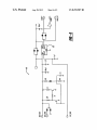
FIG. 4 is a schematic diagram of the poWer supply regula
tor circuit 44 and includes a voltage regulator 60 intercon
nected With other circuit elements, as shoWn. The poWer
35
supply regulator circuit 44 converts a vehicle battery voltage
to a regulated 5V DC for operation of the adapter 30.
FIG. 5 is a schematic diagram of the LED circuit 52. The
LED circuit 52 includes four LED control lines coupled to
four LEDs 72, 74, 76 and 78 through input buffers 80, 82, 84
and 86, respectively. In this embodiment, the LED 72 indi
cates that the protocol adapter 30 is being poWered, the LED
45
50
CPU 100 to serial data to the host computer 14, and vice versa.
FIG. 7 is a schematic diagram of the CPU 100, and includes
a microprocessor 102 and tWo input/output chips 104 and 106
electrically coupled as shoWn. In this embodiment, the micro
processor 102 is the model 87C196CA and the chips 104 and
106 are the model 74HC573. In the pass through mode, the
microprocessor 102 delivers data directly to the J 1708 trans
ceiver circuit 50 to the RS-232 transceiver circuit 42, and
ment, the interface chip 120 is the model 74HC241. The
interface circuit 98 provides interfacing betWeen the CPU 1 00
and the I/O board 32.
The foregoing discussion discloses and describes merely
exemplary embodiments of the present invention. One skilled
in the art Will readily recogniZe from such discussion and
from the accompanying draWings and claims that various
changes, modi?cations and variations can be made therein
Without departing from the spirit and scope of the invention as
de?ned in the folloWing claims.
ule 94 is used for program storage. The module 94 is respon
sible for the permanent storage of the application data and
loader application information. The module 94 alloWs the
protocol adapter 30 to be updated With neW ?rmWare in the
?eld. The uploaded ?rmware is stored in the RAM circuit 92.
The UART circuit 96 is used for communication of asyn
chronous data to and from the programmable controller 14.
The UART circuit 96 is used to convert parallel data from the
replace legacy hardWare With the protocol adapter 30 and
maintain compatibility With their original softWare.
FIG. 9 is a schematic diagram of the CPU I/O interface
circuit 98, and includes an interface chip 120. In one embodi
the protocol adapter 30 is operating in the J 1708 protocol.
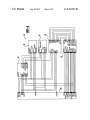
FIG. 6 is a schematic block diagram of the CPU board 34.
The CPU board 34 includes a CPU 100, a device decoder
circuit 90, a static RAM circuit 92, a ?ash memory module
94, a UART circuit 96 and a CPU I/O interface circuit 98
electrically interconnected as shoWn. The ?ash memory mod
messages. The protocol adapter 30 accommodates these over
siZed messages by putting the J1708 mailbox into extended
mode and attaching it to a location in the static RAM circuit
92. The J1939 transport layer also makes use of the RAM
circuit 92 to ensure that transport timing requirements are
met. The storing of multiple messages in the static RAM
circuit 92 reduces multiple reads and Writes to the adapter
hardWare. The concatenation of these short messages reduces
the overhead on the serial port. The static RAM circuit 92
alloWs users to replace legacy hardWare With an interface that
can support existing softWare. Consequently, users can
40
74 indicates a link to the RS-232 port 16 of the host computer
14, the LED 76 indicates that the protocol adapter 30 is
operating in the J1939 protocol and the LED 78 indicates that
messages.
Sometimes both the J1708 and the J1939 protocols trans
mit oversiZed messages. A normal J 1708 message may be up
to 21 bytes long. HoWever, special modes may utiliZe longer
number, time stamp, identi?er, length of data, etc., should be
sent to the host immediately upon receipt, and hoW the appli
provides ?exibility for transmitting and receiving messages,
regardless of the J1708 or J1939 vehicle protocol, by provid
ing a temporary message storage location, redirection of
the ID and data to be sent, the conditions for a call back
55
What is claimed is:
1. A protocol adapter for transferring diagnostic messages
betWeen a vehicle netWork in a vehicle and an external host
computer, said adapter comprising:
60
a plurality of transceiver circuits for providing an interface
betWeen the vehicle netWork and the host computer
When the vehicle netWork is operating in one of a plu
rality of protocols;
Wherein the adapter automatically sWitches to one or more
65
of the plurality of protocols the host computer is using;
and further comprising a central processing unit (CPU),
said CPU controlling the operation of the plurality of
transceiver circuits to automatically sWitch betWeen the
US 8,255,587 B2
8
7
circuits, depending on which of the plurality of protocols
the host computer is using; and
plurality of transceiver circuits, depending on which of
the plurality of protocols the host computer is using.
2. The protocol adapter according to claim 1 one of said
plurality of transceiver circuits further comprising an RS-232
transceiver, said RS-232 transceiver circuit providing an
a voltage translator for translating the voltage of one or
5
interface to an RS-232 port on the host computer.
3. The protocol adapter according to claim 1, further com
prising a device decoder, said device decoder decoding input
signals sent to the CPU.
interface to an RS-232 port on the host computer.
4. The protocol adapter according to claim 1, further com
prising a static random access memory (RAM) circuit, said
RAM circuit including a RAM that provides temporary data
storage and is connected to the CPU through data and address
channels.
11. The protocol adapter according to claim 9, further
comprising a static random access memory (RAM) circuit,
said RAM circuit including a RAM that provides temporary
data storage and is connected to said CPU through data and
address channels.
5. The protocol adapter according to claim 4 wherein the
RAM circuit further provides redirection of mailbox data,
storage for oversiZed messages and the concatenation of
12. The protocol adapter according to claim 11 wherein the
RAM circuit further provides redirection of mailbox data,
storage for oversiZed messages and the concatenation of
small messages.
small messages.
6. The protocol adapter according to claim 1, further com
prising a ?ash memory module, said ?ash memory module
13. The protocol adapter according to claim 9 further com
prising a ?ash memory module, said ?ash memory module
providing permanent storage of application data and loader
application information.
providing permanent storage of application data and loader
application information.
7. The protocol adapter according to claim 1, further com
prising a universal asynchronous receive and transmit
14. The protocol adapter according to claim 9 further com
prising a universal asynchronous receive and transmit
(UART) circuit, said UART circuit providing communication
(UART) circuit, said UART circuit providing communication
of asynchronous data to and from the host computer.
8. The protocol adapter according to claim 1, further com
prising a CPU I/O interface circuit, said CPU I/O interface
circuit providing an interface between the CPU and the trans
ceiver circuits.
9. A protocol adapter for transferring diagnostic messages
between a vehicle network in a vehicle and an external host
computer, said adapter comprising:
a plurality of transceiver circuits for providing an interface
between the vehicle network and the host computer
when the vehicle network is operating in one of a plu
rality of protocols;
a central processing unit (CPU), said CPU controlling the
operation of the plurality of transceiver circuits to auto
matically switch between the plurality of transceiver
more of said plurality of protocols, said voltage transla
tor being part of one of said plurality of transceiver
circuits.
10. The protocol adapter according to claim 9, one of said
plurality of transceiver circuits further comprising an RS-232
transceiver, said RS-232 transceiver circuit providing an
of asynchronous data to and from the host computer.
15. The protocol adapter according to claim 9, further
30
comprising a CPU I/O interface circuit, said CPU l/O inter
face circuit providing an interface between said CPU and the
transceiver circuits.
16. The protocol adapter according to claim 9, one of said
plurality of transceiver circuits further comprising a J1708
transceiver circuit, said J 1708 transceiver circuit providing an
interface between the vehicle network and the ho st computer
when the vehicle network is operating in a J1708 protocol and
the protocol adapter is operating in a pass-through mode, said
J 1708 transceiver circuit including the voltage translator for
translating the voltage of the J1708 protocol signals.
*
*
*
*
*