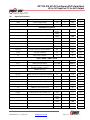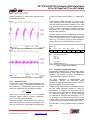
1
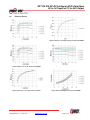
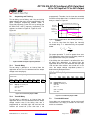
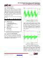
DP7120 20A DC-DC Intelligent dPOL Data Sheet
8V to 14V Input • 0.7V to 5.5V Output
Applications
• Low voltage, high density systems with
Intermediate Bus Architectures (IBA)
• Point-of-load regulators for high performance DSP,
FPGA, ASIC, and microprocessor applications
• Desktops, servers, and portable computing
• Broadband, networking, optical, and
communications systems
Benefits
• Integrates digital power conversion with intelligent
power management
• Eliminates the need for external power
management components
2
• Programmable via industry-standard I C
communication bus (DPM required)
• Reduce the number of discrete parts within a
power system.
• Reduces board space, system cost, complexity
and time to market
Features
• Input voltage range: 8V–14V
• High continuous output current: 20A
• Wide digitally programmable output voltage range:
0.7V–5.5V
• Active patented current sharing
• Single-wire serial communication bus between dPOL
and Digital Power Manager (DPM)
• Programmable dynamic output voltage positioning for
better load transient response
• Overcurrent, overvoltage, undervoltage, and
overtemperature protections with programmable
thresholds and hiccup or latching modes
• Programmable fixed switching frequency:
500KHz or 1.0MHz
• Programmable switching phase delay
• Programmable turn-on and turn-off delays
• Programmable turn-on and turn-off output voltage
slew rates with tracking protection
• Auto Compensation
• In-System Loop Identification (SysID) through
pseudo-random noise injection
• Power Good signal with programmable threshold and
delay.
• Advanced fault management and propagation
• Start up into pre-biased load
• Real time voltage, current, and temperature
measurements, monitoring, and reporting
• Small footprint Vertical oriented SMT package:
8x32mm
• Low profile of 14mm
• Compatible with conventional pick-and-place
equipment
• Wide operating temperature range -40°C - 85°C
• UL 60950-1/CSA 22.2 No. 60950-1-07 Second
Edition, IEC 60950-1: 2005, and EN 60950-1:2006
(pending)
Description
Power-One’s DP7120 is an intelligent, fully programmable step-down point-of-load DC-DC converter integrating
digital power conversion and intelligent power management. The dPOL is used in conjunction with DM73xx Series
Digital Power Manager (DPM), and completely eliminates the need for external components for output voltage
setting, sequencing, tracking, protection, monitoring, error amplifier compensation and reporting. All performance
parameters of the DP7120 are programmable and managed through Digital Power Manager via the industry2
standard I C communication bus and can be changed by a user at any time during product development and
operation. Telemetry data is available in real time and can be accessed over the I²C bus.
BCD.00259 Rev. 1.0, 12 Feb 2013
www.power-one.com
Page 1 of 37
DP7120 20A DC-DC Intelligent dPOL Data Sheet
8V to 14V Input • 0.7V to 5.5V Output
Reference Documents:
• DM7300 Digital Power Manager Data Sheet
• DM7300 Digital Power Manager Programming Manual
• Power-One I2C GEN II Graphical User Interface
2
• DM00056-KIT USB to I C Adapter Kit. User Manual
1.
Ordering Information
DP
71
Product
family:
Series:
Intelligent
dPOL
Converter
20
G
–
zz
1
®
dPWER
Packaging Option
R100 - 100pcs T&R
RoHS compliance:
Output
Current:
20A
G - RoHS compliant for all six
substances
Dash
Q1 – 1pc sample for evaluation only
Example: DP7120G-R100: A 100-piece reel of RoHS compliant dPOL converters. Each dPOL converter is
labeled DP7120G. (Larger reel sized not available)
2.
Absolute Maximum Ratings
Stresses in excess of the absolute maximum ratings may cause performance degradation, adversely affect longterm reliability, and cause permanent damage to the converter.
3.
Parameter
Conditions/Description
Min
Max
Units
Inductor or
Printed Circuit Board (PCB)
Temperature
Input Voltage applied
-40
125
°C
Input Voltage
250ms Transient
15
VDC
Output Current
(See Output Current De-rating Curves)
20
ADC
-16
Environmental and Mechanical Specifications
Parameter
Conditions/Description
Min
Nom
Units
Ambient Temperature Range
-40
85
°C
Storage Temperature (Ts)
-55
125
°C
15
grams
Weight
1
Max
MTBF
Calculated Per Telcordia Technologies SR-332
6.24
MHrs
Peak Reflow Temperature
DP7120G
245
Lead Plating
DP7120G
100% Matte Tin
Moisture Sensitivity Level
DP7120G
3
Packaging option is used only for ordering and not included in the part number printed on the dPOL converter label.
BCD.00259 Rev. 1.0, 12 Feb 2013
www.power-one.com
Page 2 of 37
260
°C
DP7120 20A DC-DC Intelligent dPOL Data Sheet
8V to 14V Input • 0.7V to 5.5V Output
4.
Electrical Specifications
Specifications apply at the input voltage from 8V to 14V, output load from 0 to 20A, ambient temperature from
-40°C to 85°C. Test conditions include an output filter with 3 x 330µF 20mΩ solid electrolytic plus 2 x 22µF X7R
ceramic output capacitors, unless otherwise noted..
4.1.
Input Specifications
Parameter
Conditions/Description
Input voltage (VIN)
4.2.
Min
Nom
8
Input Current (at no load)
VIN=14.0V, VOUT=3.3V
Undervoltage Lockout
Ramping Up
Ramping Down
VLDO Input Current
Current drawn from the external low
voltage supply at VLDO=8V
Max
1electrol
ytic4
50
VDC
mADC
7.5
5
Units
50
VDC
VDC
mADC
Output Specifications
Parameter
Conditions/Description
Min
Output Voltage Range (VOUT)
Output Voltage Setpoint
Resolution
Output Voltage Setpoint Accuracy
Nom
0.7
Max
Units
5.5
VDC
2.5mV (1LSB)
2
nd
Vo Loop Enabled
±(0.6% + 5mV)
2
Output Current (IOUT)
VIN MIN to VIN MAX
Line Regulation
VIN MIN to VIN MAX
±0.3
%VOUT
0 to IOUT MAX
±0.2
%VOUT
50
60
mV
µs
10
20
40
18
35
50
mV
mV
mV
mV
mV
mV
VIN=12V, IOUT=0.5×IOUT MAX
20
ppm/°C
Default
Programmable to
Default
Programmable, 1.56% steps
500
500 / 1,000
90.5
Load Regulation
Dynamic Regulation
Peak Deviation
Settling Time
Output Voltage Peak-to-Peak
Ripple and Noise
Scope BW=20MHz
Full Load
Temperature Coefficient
Switching Frequency
Duty Cycle Limit
-5.5
Slew rate 1A/µs, 50 -75% load step
FSW=500kHz
to 10% of peak deviation
See Output Load Transient Section
VIN=8.0V, VOUT=0.7V
VIN=8.0V, VOUT=2.5V
VIN=8.0V, VOUT=5.5V
VIN=14V, VOUT=0.7V
VIN=14V, VOUT=2.5V
VIN=14V, VOUT=5.5V
20
3.125
ADC
kHz
100
%
%
2
At negative (sink) output current (bus terminator mode) the efficiency of the DP7120 degrades resulting in increased internal power
dissipation and switching noise. Therefore maximum allowable negative current under specific conditions is lower than the current determined
from the de-rating curves shown in paragraph.
BCD.00259 Rev. 1.0, 12 Feb 2013
www.power-one.com
Page 3 of 37
DP7120 20A DC-DC Intelligent dPOL Data Sheet
8V to 14V Input • 0.7V to 5.5V Output
4.3.
Protection Specifications
Parameter
Conditions/Description
Min
Nom
Max
Units
Non-Latching, 130ms period
Latching/Non-Latching
132
36
132
%IOUT
%IOUT
Output Overcurrent Protection
Default
Programmable
Default
Programmable in 11 steps
Type
Threshold
Threshold Accuracy
-20
+20
%IOCP.SET
Non-Latching, 130ms period
Latching/Non-Latching
130
110
130
%VO.SET
%VO.SET
Output Overvoltage Protection
Default
Programmable
Default
Programmable in 10% steps
Type
Threshold
Threshold Accuracy
Measured at VO.SET=2.5V
Delay
From instant when threshold is exceeded until
the turn-off command is generated
6
Default
Emergency Off
Programmable to
Critical Off / Emergency Off
3
Turn Off Behavior
-2
2
%VOVP.SET
µs
Output Undervoltage Protection
Default
Programmable
Default
Programmable in 5% steps
Type
Threshold
Non-Latching, 130ms period
Latching/Non-Latching
75
75
90
Threshold Accuracy
Measured at VO.SET=2.5V
Delay
From instant when threshold is exceeded until
the turn-off command is generated
6
Default
Sequenced Off
Programmable to
Sequenced / Critical Off
Turn Off Behavior
3
-2
2
%VO.SET
%VO.SET
%VUVP.SET
µs
Overtemperature Protection
Type
Default
Programmable
Non-Latching, 130ms period
Latching/Non-Latching
Turn Off Threshold
Temperature is increasing
120
°C
Turn On Threshold
Temperature is decreasing after the module was
4
shut down by OTP
110
°C
Threshold Accuracy
Delay
Turn Off Behavior
3
-5
From instant when threshold is exceeded until
the turn-off command is generated
Default
Programmable to
5
6
°C
µs
Sequenced Off
Sequenced / Critical Off
Tracking Protection (when Enabled)
3
Sequenced Off: The turn-off follows the turn-off delay and slew-rate settings; Critical Off: At turn-off both low and high switches are
immediately disabled; Catastrophic Off: At turn-off the high side switch is disabled and the low side switch is enabled.
OTP clears when Overtemp Warning (Status Register TW bit) turns off.
4
BCD.00259 Rev. 1.0, 12 Feb 2013
www.power-one.com
Page 4 of 37
DP7120 20A DC-DC Intelligent dPOL Data Sheet
8V to 14V Input • 0.7V to 5.5V Output
Type
Default
Programmable
Threshold
Enabled during output voltage ramping up
Threshold Accuracy
Disabled
Latching/Non-Latching, 130ms
-50
Delay
From instant when threshold is exceeded until
the turn-off command is generated
Threshold
Always enabled, reported in Status register (TW
5
bit)
Threshold Accuracy
From Nominal Set Point
±250
mVDC
50
mVDC
6
µs
110
°C
Overtemperature Warning
-5
Hysteresis
+5
1.7
°C
°C
Power Good Signal (PG pin)
Logic
Lower Threshold
Upper Threshold
Threshold Accuracy
6
PG On Delay
VOUT is inside the PG window
VOUT is outside the PG window
Default
Programmable in 5% steps
Default
Programmable in 5% steps
105
110
Measured at VO.SET=2.5V
-2
2
Default
Programmable at
Default
PG Off Delay
Programmable same as PG On Delay
5
6
High
Low
90
90
95
110
0
0, 10, 50, 150
PG disabled when VOUT ≤ VUV
threshold
PG disabled at turn-off command
(Reset function)
Temp Warning error same sign and proportional with OTP error.
From instant when threshold is exceeded until status of PG signal changes high
BCD.00259 Rev. 1.0, 12 Feb 2013
www.power-one.com
Page 5 of 37
%VO.SET
%VO.SET
%VO.SET
%VO.SET
ms
DP7120 20A DC-DC Intelligent dPOL Data Sheet
8V to 14V Input • 0.7V to 5.5V Output
4.4.
Feature Specifications
Parameter
Conditions/Description
Min
Nom
Max
Units
Current Share
Type
Active, Single Line
Maximum Number of Modules
Connected in Parallel
IOUT ≥ 20% IOUT NOM
Current Share Accuracy
IOUT ≥ 20% IOUT NOM
Interleave (Phase Shift)
Default
Programmable in 22.5° steps
4
±20
%IOUT
337.5
Degree
degree
Interleave
0
0
7
Sequencing
Turn ON Delay
Turn OFF Delay
Default
Programmable in 1ms steps
Default
Programmable in 1ms steps
0
0
255
0
0
63
ms
ms
ms
ms
Tracking
Turn ON Slew Rate
Turn OFF Slew Rate
Default
Programmable in 8 steps
Default
Programmable in 8 steps
0.05
0.05
8
2.0
-0.05
-0.05
-2.0
8
V/ms
V/ms
V/ms
V/ms
Optimal Voltage Positioning
Load Regulation
Default
Programmable in 7 steps
0
0
2.45
mV/A
mV/A
Feedback Loop Compensation
Proportional (Kr)
Programmable
0.01
2
Integral (Ti)
Programmable
1
100
µs
Differential (Td)
Programmable
1
100
µs
Differential Roll-Off (Tv)
Programmable
1
100
µs
Monitoring
Voltage Monitoring Accuracy
12 Bit Resolution over 0.5…5.5V
-0.5
0.5
%
Current Monitoring Accuracy
20% IOUT NOM < IOUT < IOUT NOM
-20
+20
%IOUT
Temperature Monitoring Accuracy
Junction temperature of dPOL
controller
-5
+5
°C
9
Remote Voltage Sense (+VS and –VS pins)
Voltage Drop Compensation
Between +VS and VOUT
300
mV
Voltage Drop Compensation
Between -VS and PGND
100
mV
7
Timing based on SD clock and subject to tolerances of SD.
Achieving fast slew rates under specific line and load conditions may require feedback loop adjustment. See Rising and Falling Slew Rates..
9
For remote sense, it is recommended to place a 0.01-0.1µF ceramic capacitor between +VS and –VS pins as close to the dPOL converter
as possible.
8
BCD.00259 Rev. 1.0, 12 Feb 2013
www.power-one.com
Page 6 of 37
DP7120 20A DC-DC Intelligent dPOL Data Sheet
8V to 14V Input • 0.7V to 5.5V Output
4.5.
Signal Specifications
Parameter
Conditions/Description
Min
Nom
Max
Units
VDD
Internal supply voltage
3.15
3.3
3.45
V
Logic In Max
Pull Up Logic max safe input
VDD+.5
V
0.3 x VDD
V
VDD + 0.5
V
0.45 x
VDD
V
60
mA
300
ns
10
pF
SYNC/DATA Line (SD pin)
ViL_sd
LOW level input voltage
-0.5
ViH_sd
HIGH level input voltage
Vhyst_sd
Hysteresis of input Schmitt trigger
VoL
LOW level sink current @ 0.5V
Tr_sd
Maximum allowed rise time 10/90%VDD
Cnode_sd
Added node capacitance
Ipu_sd
Pull-up current source at Vsd=0V
0.3
1.0
mA
Freq_sd
Clock frequency of external SD line
475
525
kHz
Tsynq
Sync pulse duration
22
28
T0
Data=0 pulse duration
72
78
0.75 x
VDD
0.25 x
VDD
14
5
% of clock
cycle
% of clock
cycle
Inputs: ADDR0…ADDR4, EN, IM
ViL_x
LOW level input voltage
-0.5
0.3 x VDD
V
ViH_x
HIGH level input voltage
0.7 x VDD
VDD+0.5
V
Vhyst_x
Hysteresis of input Schmitt trigger
0.1 x VDD
0.3 x VDD
V
RdnL_ADDR
External pull down resistance
ADDRX forced low
10
kOhm
Power Good and OK Inputs/Outputs
Iup_PG
Pull-up current source input forced low PG
25
110
µA
Iup_OK
Pull-up current source input forced low OK
175
725
µA
ViL_x
LOW level input voltage
-0.5
0.3 x VDD
V
ViH_x
HIGH level input voltage
0.7 x VDD
VDD+0.5
V
Vhyst_x
Hysteresis of input Schmitt trigger
0.1 x VDD
0.3 x VDD
V
IoL
LOW level sink current at 0.5V
4
20
mA
0.84
3.1
mA
-0.5
0.3 x VDD
V
VDD+0.5
V
0.45 x
VDD
V
60
mA
100
ns
Current Share Bus (CS pin)
Iup_CS
Pull-up current source at VCS = 0V
ViL_CS
LOW level input voltage
ViH_CS
HIGH level input voltage
Vhyst_CS
Hysteresis of input Schmitt trigger
IoL
LOW level sink current at 0.5V
Tr_CS
Maximum allowed rise time 10/90% VDD
BCD.00259 Rev. 1.0, 12 Feb 2013
www.power-one.com
0.75 x
VDD
0.25 x
VDD
14
Page 7 of 37
DP7120 20A DC-DC Intelligent dPOL Data Sheet
8V to 14V Input • 0.7V to 5.5V Output
5.
Pin Assignments and Descriptions
Pin
Name
Pin
Number
Pin
Type
VIN
1
NC
IM
Buffer
Type
Pin Description
Notes
Not Used
No internal connection
2
Not Used
Leave floating
NC
3
Not Used
Leave floating
NC
4
Not Used
Leave floating
NC
5
Not Used
Leave floating
NC
6
Not Used
Leave floating
NC
7
Not Used
Leave floating
NC
8
Not Used
Leave floating
VREF
9
Not Used
Nominally 2.5V. Leave unconnected
EN
10
Not Used
Leave floating or connect to PGND
OK
11
I/O
PU
Fault/Status Condition
Connect to OK pin of the DPM and any other
dPOLs of the same group.
SD
12
I/O
PU
Sync/Data Line
Connect to SD pin of DPM
PG
13
I/O
PU
Power Good
Pin state reflected in Status Register.
TRIM
14
Not Used
Leave floating
CS
15
I/O
PU
Current Share
Connect to CS pins of other dPOLs connected in
parallel. Leave floating if not on shared bus.
ADDR4
16
I
PU
dPOL Address Bit 4
Tie to PGND for 0 or leave floating for 1
ADDR3
17
I
PU
dPOL Address Bit 3
Tie to PGND for 0 or leave floating for 1
ADDR2
18
I
PU
dPOL Address Bit 2
Tie to PGND for 0 or leave floating for 1
ADDR1
19
I
PU
dPOL Address Bit 1
Tie to PGND for 0 or leave floating for 1
ADDR0
20
I
PU
dPOL Address Bit 0
Tie to PGND for 0 or leave floating for 1
-VS
21
I
PU
Negative Voltage Sense
+VS
22
I
PU
Positive Voltage Sense
VOUT
23
P
Output Voltage
PGND
24
P
Power Ground
VIN
25
P
Input Voltage
A
Connect to the negative point close to the load or
PGND
Connect to the positive point close to the load or
VOUT
Legend: I=input, O=output, I/O=input/output, P=power, A=analog, PU=internal pull-up, NC=No Connection
BCD.00259 Rev. 1.0, 12 Feb 2013
www.power-one.com
Page 8 of 37
DP7120 20A DC-DC Intelligent dPOL Data Sheet
8V to 14V Input • 0.7V to 5.5V Output
6.
Typical Performance Characteristics
6.1.
Thermal De-rating Curves
24
25
20
Load Current [Adc]
Load Current [Adc]
20
16
12
500 LFM (2.5 m/s)
400 LFM (2.0 m/s)
300 LFM (1.5 m/s)
200 LFM (1.0 m/s)
100 LFM (0.5 m/s)
30 LFM (0.15 m/s)
8
4
30
40
500 LFM (2.5 m/s)
400 LFM (2.0 m/s)
300 LFM (1.5 m/s)
200 LFM (1.0 m/s)
100 LFM (0.5 m/s)
30 LFM (0.15 m/s)
10
5
0
20
15
50
60
70
80
0
90
20
30
40
Ambient Temperature [°C]
Figure 1.
Available output current vs. ambient air
temperature and airflow rates for converter
DP7120 mounted horizontally with air flowing
from input to output, MOSFET temperature ≤ 120
°C, Vin = 8 V, Vout = 5 V, and Fsw= 500KHz
60
70
80
90
Figure 3. Available output current vs. ambient air temperature
and airflow rates for converter DP7120 mounted
horizontally with air flowing from input to output,
MOSFET temperature 120 C, Vin = 12 V, Vout = 5
V, and Fsw= 500KHz
18
18
15
15
Load Current [Adc]
Load Current [Adc]
50
Ambient Temperature [°C]
12
9
500 LFM (2.5 m/s)
400 LFM (2.0 m/s)
300 LFM (1.5 m/s)
200 LFM (1.0 m/s)
100 LFM (0.5 m/s)
30 LFM (0.15 m/s)
6
3
30
40
50
60
70
80
90
Ambient Temperature [°C]
Figure 2.
9
500 LFM (2.5 m/s)
400 LFM (2.0 m/s)
300 LFM (1.5 m/s)
200 LFM (1.0 m/s)
100 LFM (0.5 m/s)
30 LFM (0.15 m/s)
6
3
0
20
12
20
30
40
50
60
70
80
90
Ambient Temperature [°C]
Available output current vs. ambient air
temperature and airflow rates for converter
DP7120 mounted horizontally with air flowing
from input to output, MOSFET temperature ≤ 120
°C, Vin = 8 V, Vout = 5 V, and Fsw= 1MHz
BCD.00259 Rev. 1.0, 12 Feb 2013
0
www.power-one.com
Figure 4. Available output current vs. ambient air temperature
and airflow rates for converter DP7120 mounted
horizontally with air flowing from input to output,
MOSFET temperature 120 C, Vin = 12 V, Vout = 5
V, and Fsw= 1MHz
Page 9 of 37
DP7120 20A DC-DC Intelligent dPOL Data Sheet
8V to 14V Input • 0.7V to 5.5V Output
6.2.
Efficiency Curves
Figure 5. Efficiency vs. Load. Vin=12V, Fsw=500kHz
Figure 8. Efficiency vs. Output Voltage, Iout=7A, Fsw=500kHz
Figure 6 Efficiency vs Load. Vin=8V, Fsw=500KHz
Figure 9. Efficiency vs Vin. Fsw=500kHz
Figure 7 Efficiency vs Vout at Vin=12V, Load=20A
BCD.00259 Rev. 1.0, 12 Feb 2013
www.power-one.com
Figure 10 Power Dissipation Vin=12V, Fsw=500KHz
Page 10 of 37
DP7120 20A DC-DC Intelligent dPOL Data Sheet
8V to 14V Input • 0.7V to 5.5V Output
Figure 11 Effciency vs Load, Vin=12V, Fsw=1MHz
Figure 12 Efficiency vs Load, Vin=8V, Fsw=1MHz
BCD.00259 Rev. 1.0, 12 Feb 2013
www.power-one.com
Figure 13 Efficiency vs Vin, Fsw=1MHz
Figure 14 Dissipation vs Load. Vin=12V, Fsw=1MHz
Page 11 of 37
DP7120 20A DC-DC Intelligent dPOL Data Sheet
8V to 14V Input • 0.7V to 5.5V Output
7.
Programmable Features
7.1.
Performance parameters of DP7120 dPOL
converters can be programmed via the industry
2
standard I C communication bus. Each parameter
has a default value stored in the volatile memory
registers detailed in Table 1. The setup registers 00h
through 14h are programmed at the system powerup. When the user programs new performance
parameters, the values in the registers are
overwritten. Upon removal of the input voltage, the
default values are restored.
Output Voltage
The output voltage can be programmed in the GUI
Output Configuration window shown in the Figure 15
2
or directly via the I C bus by writing into the VOS
register shown in Figure 16.
DP7120 converters can be programmed using the
2
Graphical User Interface or directly via the I C bus by
using high and low level commands as described in
the ‘”DPM Programming Manual”.
DP7120 parameters can be reprogrammed at any
time during the system operation and service except
for the digital filter coefficients, the switching
frequency and the duty cycle limit, that can only be
changed when the dPOL output is turned off.
CONFIGURATION REGISTERS
Name
Register
PC1
Protection Configuration 1
PC2
Protection Configuration 2
PC3
Protection Configuration 3
TC
Tracking Configuration
INT
Interleave and Frequency Configuration
DON
Turn-On Delay
DOF
Turn-Off Delay
VLC
Voltage Loop Configuration
CLS
Current Limit Set-point
DCL
Duty Cycle Limit
PC4
Protection Configuration 4
V1H
Output Voltage Setpoint 1 (Low Byte)
V1L
Output Voltage Setpoint 1 (High Byte)
V2H
Output Voltage Setpoint 2 (Low Byte)
V2L
Output Voltage Setpoint 2 (High Byte)
V3H
Output Voltage Setpoint 3 (Low Byte)
V3L
Output Voltage Setpoint 3 (High Byte)
CP
Controller Proportional Coefficient
CI
Controller Integral Coefficient
CD
Controller Derivative Coefficient
B1
Controller Derivative Roll-Off Coefficient
STATUS REGISTERS
Name
Register
RUN
Run enable / status
ST
Status
MONITORING REGISTERS
Name
Register
VOH
Output Voltage High Byte (Monitoring)
VOL
Output Voltage Low Byte (Monitoring)
IO
Output Current (Monitoring)
TMP
Temperature (Monitoring)
Address
0x00
0x01
0x02
0x03
0x04
0x05
0x06
0x07
0x08
0x09
0x0A
0x0B
0x0C
0x0D
0x0E
0x0F
0x10
0x11
0x12
0x13
0x14
Address
0x15
0x16
Address
0x17
0x27
0x18
0x19
Figure 15. Output Configuration Window
Note that the GUI shows the effect of setting PG, OV
and UV limits as both values and graphical limit bars.
Vertical hashed lines are error bars for the
Overcurrent (OC) limit.
7.1.1. Output Voltage Setpoint
The output voltage programming range is from 0.7 V
to 5.5 V. The resolution is constant across the range
and is 2.5 mV. A Total of 3 registers are provided:
one should be used for the normal setpoint voltage;
the other two can be used to define a low/high
margining voltage setpoint. Note that each register is
16bit wide and that the high byte needs always to be
written / read first. The writing of the low byte triggers
the refresh of the whole 16bit register (the high byte
is written to a shadow register).
Unlike other configuration registers, the dPOL
controller's VOS registers are dynamic. Changes to
VOS values can be made while the output is enabled
over the I2C bus through register bypass commands
and the dPOL will change its output immediately.
Table 1. DP7120 Memory Registers
BCD.00259 Rev. 1.0, 12 Feb 2013
www.power-one.com
Page 12 of 37
DP7120 20A DC-DC Intelligent dPOL Data Sheet
8V to 14V Input • 0.7V to 5.5V Output
VOS: Output Voltage Set-Point
Address: 0x0B … 0x10
Coefficient
V1H First Vo Setpoint High Byte
V1L First Vo Setpoint Low Byte
V2H Second Vo Setpoint High Byte
V2L
Second Vo Setpoint Low Byte
V3H Third Vo Setpoint High Byte
V3L
Third Vo Setpoint Low Byte
Mapping:
- 12 bit data word, left aligned
- 1LSB = 2.5mV
Addr
0x0B
0x0C
0x0D
0x0E
0x0F
0x10
Bits
8
8
8
8
8
8
Default
bus. In the DP7007 Load Regulation can be set to
one of eight values: 0, 0.37, 0.74, 1.11, 1.48, 1.85,
2.23, or 2.6 mV/A.
Figure 18 shows a DP7120 dPOL with 0 mV/A (load
current) regulation. Alternating high and low output
load currents causes large transients in Vout to
appear with each change.
Note:
- all registers are readable and writeable
- always write and read the high byte first
Figure 16. Output Voltage Setpoint Register VOS
7.1.2. Output Voltage Margining
If the output voltage needs to be varied by a certain
percentage, the margining function can be utilized.
The margining can be programmed in the dPOL
2
Configuration window or directly via the I C bus
using high level commands as described in the
”DM7300 Digital Power Manager Programming
Manual”.
In order to properly margin dPOLs that are
connected in parallel, the dPOLs must be members
of one of the Parallel Buses. Refer to the GUI
System Configuration Window shown in Figure 55.
Figure 18 Transient Response with Regulation set to 0 mV/A.
As the Load Regulation parameter is increased, step
offsets in output voltage begin to appear, as shown
in Figure 19, with non-zero Regulation.
VOUT
Upper Regulation
Limit
Lower Regulation
Limit
Operating
Point
VI Curve Without
Load Regulation
VI Curve With
Load Regulation
Headroom without
Load Regulation
Headroom with
Load Regulation
Light
Load
IOUT
Heavy
Load
Figure 17. Optimal Voltage Positioning Concept
7.1.3. Output Load Regulation Control
When Load Regulation is programmed to be nonzero, the output voltage will decrease as the output
current increases, so the VI characteristic will have a
negative slope at the point of regulation This can be
programmed in the GUI Output Configuration
2
window shown in Figure 15 or directly via the I C
BCD.00259 Rev. 1.0, 12 Feb 2013
www.power-one.com
Figure 19 Transient response with Regulation set to 074
mV/A.
The Load Regulation parameter is an important part
of Current Sharing. It is used to set one dPOL as a
"master" and all others sharing the load as "slaves".
The dPOL with the lowest Regulation parameter sets
the effective overall regulation. (See Current Sharing
elsewhere in this document.)
Page 13 of 37
DP7120 20A DC-DC Intelligent dPOL Data Sheet
8V to 14V Input • 0.7V to 5.5V Output
7.2.
Sequencing and Tracking
Turn-on delay, turn-off delay, and rising and falling
output voltage slew rates can be programmed in the
dPOL Configure Sequencing window shown in
Figure 20 or directly via the I2C bus by writing into
the DON, DOF, and TC registers, respectively. The
registers are shown in Figure 21, Figure 23, and
Figure 24.
programmed). Therefore, for the slew rate controlled
turn-off the ramp-down time is included in the turn-off
delay as shown in Figure 22
User programmed turn-off delay, T DF
Turn-Off
Command
Calculated
delay T D
Internal
ramp-down
command
Ramp-down time, T F
Ramp-down time, T
V OUT
Falling slew
rate dV F/dT
Time
Figure 22. Relationship between Turn-Off Delay and Falling
Slew Rate
As it can be seen from the figure, the internally
calculated delay TD is determined by the equation
below.
V
TD = TDF − OUT ,
dVF
dT
For proper operation TD shall be greater than zero.
The appropriate value of the turn-off delay needs to
be programmed to satisfy the condition.
Figure 20. dPOL Configure Sequencing Window
7.2.1. Turn-On Delay
Turn-on delay is defined as an interval from the
application of the Turn-On command until the output
voltage starts ramping up.
Address: 0x05
R/W-0
DON6
R/W-0
DON5
R/W-0
DON4
R/W-0
DON3
Bit 7:0
DON[7:0]: Turn-On delay in ms
0x00 = 0ms (default)
0x01 = 1ms
…
0xFF = 255ms
DOF: Turn-Off Delay Configuration
Address: 0x06
DON: Turn-On Delay Configuration
R/W-0
DON7
Bit 7
If the falling slew rate control is not utilized, the turnoff delay only determines an interval from the
application of the Turn-Off command until both high
side and low side switches are turned off. In this
case, the output voltage ramp-down process is
determined by load parameters.
R/W-0
DON2
R/W-0
DON1
R/W-0
DON0
Bit 0
U
--Bit 7
Bit 7:6
Bit 5:0
U
---
R/W-0
DOF5
R/W-0
DOF4
R/W-1
DOF3
R/W-0
DOF2
R/W-1
DOF1
R/W-1
DOF0
Bit 0
Unimplemented: read as ‘0’
DOF[5:0]: Turn-Off delay in ms
0x00 = 0ms
0x01 = 1ms
…
0x0B = 11ms (default)
…
0x3F = 63ms
Figure 21. Turn-On Delay Register DON
Figure 23. Turn-Off Delay Register DOF
7.2.2. Turn-Off Delay
Turn-off delay is defined as an interval from the
application of the Turn-Off command until the output
voltage reaches zero (if the falling slew rate is
programmed) or until both high side and low side
switches are turned off (if the slew rate is not
BCD.00259 Rev. 1.0, 12 Feb 2013
www.power-one.com
7.3.
Turn-On/Off Control
Once delays are accounted for, turn-on and turn-off
characteristics are simply a function of slew rates,
which are selectable.
Page 14 of 37
DP7120 20A DC-DC Intelligent dPOL Data Sheet
8V to 14V Input • 0.7V to 5.5V Output
7.3.1. Rising and Falling Slew Rates
Output voltage ramp up (and down) control is
accomplished by programming the rising and falling
slew rates of the output voltage, supported in the
GUI as shown in Figure 20, which is implemented by
the DPM through writing data to the TC register,
Figure 24.
To achieve programmed slew rates, the output
voltage is being changed in 10mV steps where
duration of each step determines the slew rate. For
example, ramping up a 1.0V output with a slew rate
of 0.5V/ms will require 100 steps duration of 20µs
each.
Duration of each voltage step is calculated by
dividing the master clock frequency generated by the
DPM. Since all dPOLs in the system are
synchronized to the master clock, the matching of
voltage slew rates of different outputs is very
accurate as it can be seen in Figure 25 and Figure
30.
ICHG = CLOAD ×
dVR
dt
Where, CLOAD is load capacitance, dVR/dt is rising
voltage slew rate, and ICHG is charging current.
When selecting the rising slew rate, a user needs to
ensure that
ILOAD + ICHG < IOCP
Where IOCP is the overcurrent protection threshold of
the dPOL. If the condition is not met, then the
overcurrent protection will be triggered during the
turn-on process. To avoid this, dVR/dt and the
overcurrent protection threshold should be
programmed to meet the condition above.
7.3.2. Delay and Slew Rate Combination
The effect of setting slew rates and turn on/off delays
is illustrated in the following sets of figures.
TC: Tracking Configuration
Address: 0x03
U
--Bit 7
Bit 7
Bit 6:4
Bit 3
Bit 2:0
R/W-0
R2
R/W-0
R1
R/W-1
R0
R/W-1
SC
R/W-1
F2
R/W-0
F1
R/W-0
F0
Bit 0
Unimplemented: read as ‘0’
R[2:0]: Vo rising slew rate
0 = 0.05 V/ms (default when in bus terminator mode)
1 = 0.1 V/ms (default)
2 = 0.2 V/ms
3 = 0.25 V/ms
4 = 0.5 V/ms
5 = 1.0 V/ms
6 = 2.0 V/ms
7 = Reserved
SC: Turn-off slew rate control
0 = disabled
1 = enabled (default)
F[2:0]: Vo falling slew rate
0 = -0.05 V/ms
1 = -0.1 V/ms
2 = -0.2 V/ms
3 = -0.25 V/ms (default when in bus terminator mode)
4 = -0.5 V/ms (default)
5 = -1.0 V/ms
6 = -2.0 V/ms
7 = Reserved
Figure 25. Tracking Turn-On. Rising Slew Rate is
Programmed at 0.5V/ms for each output.
Figure 24. Tracking Configuration Register TC
During the turn on process, a dPOL not only delivers
current required by the load (ILOAD), but also charges
the load capacitance. The charging current can be
determined from the equation below:
BCD.00259 Rev. 1.0, 12 Feb 2013
www.power-one.com
Page 15 of 37
DP7120 20A DC-DC Intelligent dPOL Data Sheet
8V to 14V Input • 0.7V to 5.5V Output
7.3.3. Pre-Bias
In some applications, power may "leak" from a
powered circuit to an unpowered bus, typically
®
through ESD protection diodes. The dPWER
controller in the dPOL holds off turn on its output
until the desired ramp up point crosses the pre-bias
point, as seen in Figure 29.
Figure 26. Turn-On with Different Rising Slew Rates.
Rising Slew Rates are V1-1V/ms, V2-0.5V/ms, V3-0.2V/ms.
Figure 29. Turn On into Prebiased Load. V3 is Prebiased by
V2 via a Diode.
Figure 27. Sequenced Turn-On. Rising Slew Rate is
Programmed at 1V/ms. V2 Delay is 2ms, V3 delay is 4ms.
This figure was captured with an actual system
where a diode was added to pre-bias a 1.5V bus
from a 1.85V bus in order to simulate the effect of
current leakage through protection circuits of
unpowered logic connected to powered logic outputs
(a common source of pre-bias in power systems).
7.4.
Turn-Off Characteristics
Turn of captures show that combining turn off delays
and ramp rates. Note that while turnoff delays have a
lower upper time limit as compared to turn on delays,
all ramp down rates are available independently to
turn on and off.
Figure 28 Two outputs delayed 5ms. All slew rates at 0.5V/ms.
BCD.00259 Rev. 1.0, 12 Feb 2013
www.power-one.com
Page 16 of 37
DP7120 20A DC-DC Intelligent dPOL Data Sheet
8V to 14V Input • 0.7V to 5.5V Output
Thresholds of overcurrent, over- and undervoltage
detection, and Power Good limits can be
programmed in the GUI Output Configuration
2
window (Figure 15) or directly via the I C bus by
writing into the PC2 registers shown in Figure 32.
Note that the overvoltage and undervoltage
protection thresholds and Power Good limits are
defined as percentages of the output voltage.
Therefore, the absolute levels of the thresholds
change when the output voltage setpoint is changed
either by output voltage adjustment or by margining.
PC2: Protection Configuration Register 2 1)
Address: 0x01
Figure 30. Tracking Turn-Off. Falling Slew Rate is
Programmed at 0.5V/ms.
U
--Bit 7
U
---
R/W-0
PGHL
R/W-0
PGLL
R/W-1
OVPL1
R/W-0
OVPL0
R/W-0
UVPL1
R/W-0
UVPL0
Bit 0
Bit7:6
Bit 5
Figure 31. Turn-Off with Tracking and Sequencing. Falling
Slew Rate is Programmed at 0.5V/ms.
7.5.
Faults, Errors and Warnings
Unimplemented: read as ‘0’
PGHL: Power Good High Level
1 = 105% of Vo
0 = 110% of Vo (default)
Bit 4
PGLL: Power Good Low Level
1 = 95% of Vo
0 = 90% of Vo (default)
Bit 3:2 OVPL: Over Voltage Protection Level
00 = 110% of Vo
01 = 120% of Vo
10 = 130% of Vo (default)
11 = 130% of Vo
Bit 1:0 UVPL: Under Voltage Protection Level
00 = 75% of Vo (default)
01 = 80% of Vo
10 = 85% of Vo
11 = 90% of Vo
1) This register can only be written when PWM is not active (RUN[RUN] is ‘0’)
Figure 32. Protection Configuration Register PC2
All dPOL series converters have a comprehensive
set of programmable fault and error protection
functions that can be classified into three groups
based on their effect on system operation: warnings,
faults, and errors. These are warnings, errors and
faults. Warnings include Thermal (Overtemperature
limit near) and Power Good (a warning in a negative
sense.)
Overcurrent limits are set either in the GUI dPOL
Output configuration dialog or in the dPOL's CLS
register as shown in Figure 33.
Note that the CLS register includes bits which control
the Regulation option settings. When writing into this
register be careful to not change Regulation by
accident.
Faults in DP7xxx and DP8xxx series dPOLs include
overcurrent protection, overvoltage, overtemperature
and tracking failure detection. Errors include only
undervoltage. Control of responses to Faults and
Errors are distributed between different dPOL
registers and are configurable in the GUI.
BCD.00259 Rev. 1.0, 12 Feb 2013
www.power-one.com
Page 17 of 37
DP7120 20A DC-DC Intelligent dPOL Data Sheet
8V to 14V Input • 0.7V to 5.5V Output
CLS: Current Limit Setting
Address: 0x08
R/W-0
LR2
Bit 7
R/W-0
LR1
Bit 7:5
LR[2:0]: Load Regulation setting
0 = 0 V/A/Ω (default)
1 = 0.39 V/A/Ω
2 = 0.78 V/A/Ω
3 = 1.18 V/A/Ω
4 = 1.57 V/A/Ω
5 = 1.96 V/A/Ω
6 = 2.35 V/A/Ω
7 = 2.75 V/A/Ω
TCE: Temperature Compensation for Current Limitation Enable
0 = disabled
1 = enabled (default)
CLS[3:0]: Current Limit set-point when Vo Stationary or Falling
0x0 = 37%
0x1 = 47%
…
0xB = 140% (default)
values higher than 0xB are translated to 0xB (140%)
Bit 4
Bit 3:0
R/W-0
LR0
R/W-1
TCE
R/W-1
CL3
R/W-0
CL2
R/W-1
CL1
R/W-1
CL0
Bit 0
Figure 33. Current Limit Setpoint Register CLS
7.5.1. Warnings
This group includes Overtemperature Warning and
Power Good Signal. Warnings do not turn off dPOLs
but rather generate signals that can be transmitted to
2
a host controller via the I C bus.
7.5.1.1. Overtemperature Warning
The Overtemperature Warning is generated when
temperature of the controller exceeds 120°C. The
Overtemperature Warning changes the TW bit of the
status register ST. When the temperature falls below
117°C, the PT bit is cleared and the
Overtemperature Warning is removed.
7.5.1.2. Power Good
Power Good (PG) is an open collector output that is
pulled low, if the output voltage is outside of the
Power Good window. The window is formed by the
Power Good High threshold that is programmable at
105 or 110% of the output voltage and the Power
Good Low threshold that can be programmed at 90
or 95% of the output voltage.
Power Good protection is only enabled after the
output voltage reaches its steady state level. A
programmable delay can be set between 0 and
150ms to delay the release of the PG pin after the
voltage has reached the steady state level (see
BCD.00259 Rev. 1.0, 12 Feb 2013
www.power-one.com
Figure 20). This allows using the PG pin to reset load
circuits properly. The Power Good protection
remains active during margining voltage transitions.
The threshold will vary proportionally to the voltage
change (see Figure 34).
The Power Good Warning pulls the PG pin low and
changes the PG bit of the status register ST to 0.
When the output voltage returns within the Power
Good window, the PG pin is released high, the PG
bit is cleared and the Power Good Warning is
removed. The Power Good pin can also be pulled
low by an external circuit to initiate the Power Good
Warning.
At turn-off the PG pin can be programmed to either
be pulled low immediately following the turn-off
command, or then when the voltage actually starts to
ramp down (Reset vs. Power Good functionality in
Figure 20).
Note: To retrieve status information, Status Monitoring in the GUI
DPM Configure Devices window should be enabled (refer to
Digital Power Manager Data Sheet). The DPM will retrieve
the status information from each dPOL on a continuous
basis.
7.5.2. Faults
This group includes overcurrent, overtemperature,
undervoltage, and tracking protections. Triggering
any protection in this group will turn off the dPOL.
For UV and OT faults the turn-off can be
programmed to sequenced or critical turn-off
behavior:
7.5.2.1. Overcurrent Protection
Overcurrent protection is active whenever the output
voltage of the dPOL exceeds the prebias voltage (if
any). When the output current reaches the OC
threshold, the POL control chip asserts an OC fault.
The dPOL sets the OC bit in the register ST to 0.
Both high side and low side switches of the dPOL
are turned off instantly (fast turn-off).
Current sensing is across the dPOLs choke. To
compensate for copper winding TC, compensation is
added to keep the OC threshold approximately
constant at temperatures above room temperature.
Note that the temperature compensation can be
disabled in the dPOL Configure Output window or
2
directly via the I C by writing into the CLS register.
However, it is recommended to keep the
temperature compensation enabled.
Page 18 of 37
DP7120 20A DC-DC Intelligent dPOL Data Sheet
8V to 14V Input • 0.7V to 5.5V Output
clamping diodes between different voltage rails
which are frequently recommended by ASIC
manufacturers.
7.5.2.2. Undervoltage Protection
The undervoltage protection is only active during
steady state operation of the dPOL to prevent
nuisance tripping. If the output voltage decreases
below the UV threshold and there is no OC fault, the
UV fault signal is generated, the dPOL turns off, and
the UV bit in the register ST is changed to 0. The
output voltage is ramped down according to
sequencing and tracking settings (regular turn-off).
When the tracking protection is enabled, the dPOL
continuously compares actual value of the output
voltage to its programmed value as defined by the
output voltage and its rising slew rate. If absolute
value of the difference exceeds 250mV, the tracking
fault signal is generated, the dPOL turns off, and the
TR bit in the register ST is changed to 0. Both high
side and low side switches of the dPOL are turned
off instantly (fast turn-off).
7.5.2.3. Overtemperature Protection
Overtemperature protection is active whenever the
dPOL is powered up. If temperature of the controller
exceeds 120°C, the OT fault is generated, dPOL
turns off, and the OT bit in the register ST is changed
to 0. The output voltage is ramped down according
to sequencing and tracking settings (regular turn-off).
The tracking protection can be disabled, if it
contradicts requirements of a particular system (for
example turning into high capacitive load where
rising slew rate is not important). It can be disabled
in the dPOL Configure Fault window or directly via
2
the I C bus by writing into the PC1 register.
If non-latching OTP is programmed, the dPOL will
restart as soon as the temperature of the controller
decreases below the Overtemperature Warning
threshold of 110°C.
7.5.3.
Faults and Margining
As noted earlier, UV and OV protection settings are
a percentage of Vout. As Vout ramps between
nominal, low or high margin values, UVP and OVP
limits adjust accordingly This is illustrated in Figure
34. The middle Vo (Vout) level is the result of a Low
Margining command. It shuts off when PG is
asserted.
7.5.2.4. Tracking Protection
Tracking protection is active only when the output
voltage is ramping up. The purpose of the protection
is to ensure that the voltage differential between
multiple rails being tracked does not exceed 250mV.
This protection eliminates the need for external
Vo
RUN
OC enabled
PG enabled
Vo_Rise
Vo_Stable
H
K_
TR
1.0V
pre-biased output
TR
L
K_
Vo_Fall
Vo_Stable
Vo_Rise
Vo_Stable
OVP Limit
OVP Limit
PG High Limit
PG High Limit
Vo_Fall
OVP Limit
PG High Limit
Vo
PGLow Limit
UVP Limit
PGLow Limit
PGLow Limit
UVP Limit
UVP Limit
Time
Figure 34. Protection Enable Conditions
BCD.00259 Rev. 1.0, 12 Feb 2013
www.power-one.com
Page 19 of 37
DP7120 20A DC-DC Intelligent dPOL Data Sheet
8V to 14V Input • 0.7V to 5.5V Output
7.5.4. Errors
The group includes overvoltage protection.
PC1: Protection Configuration Register 1
7.5.4.1. Overvoltage Protection
R/W-0
TRE
Bit 7
R/W-1
PVE
Bit 7
TRE: Tracking fault enable
1 = enabled
0 = disabled
PVE: Phase voltage error enable
1 = enabled
0 = disabled
TRC: Tracking Fault Protection Configuration
1 = latching
0 = non-latching
OTC: Over Temperature Protection Configuration
1 = latching
0 = non-latching
OCC: Over Current Protection Configuration
1 = latching
0 = non- latching
UVC: Under Voltage Protection Configuration
1 = latching
0 = non- latching
OVC: Over Voltage Protection Configuration
1 = latching
0 = non- latching
PVC: Phase Voltage Protection Configuration
1 = latching
0 = non- latching
The overvoltage protection is active whenever the
output voltage of the dPOL exceeds the pre-bias
voltage (if any). If the output voltage exceeds the
overvoltage protection threshold, the overvoltage
error signal is generated, the dPOL turns off, and the
OV bit in the register ST is changed to 0. The high
side switch is turned off instantly, and simultaneously
the low side switch is turned on to ensure reliable
protection of sensitive loads. The low side switch
provides low impedance path to quickly dissipate
energy stored in the output filter and achieve
effective voltage limitation. The OV threshold can be
programmed from 110% to 130% of the output
voltage setpoint, but not lower than 0.5V. Also the
OV threshold will always be at least 0.25V above the
setpoint.
Address: 0x00
Bit 6
Bit 5
Bit 4
Bit 3
Bit 2
Bit 1
7.5.5. Fault and Error Latching
The user has the option of setting up any protection
option
as
either
latching/non-latching
and
propagating or non-propagating.
Propagation and Latching for each dPOL is set in the
2
GUI (Figure 35 below) or directly via the I C by
writing into the PC1 register shown in Figure 36.
Bit 0
R/W-0
TRC
R/W-0
OTC
R/W-0
OCC
R/W-0
UVC
R/W-1
OVC
R/W-1
PVC
Bit 0
Figure 36. Protection Configuration Register PC1
7.5.6.
Fault and Error Turn Off Control
In the GUI dPOL Fault dialog is a column of spin
controls which set the Turn-Off style OT, UV and OV
events. The choices are defined as:
Sequenced: Outputs shut down according to ramp
down rate control settings.
Critical: Both high side and low side switches of the
dPOL are turned off instantly
Figure 35. GUI dPOL Fault Propagation Option Window
If the non-latching protection is selected, a dPOL will
attempt to restart every 130ms until the condition
that triggered the protection is removed. When
restarting, the output voltages follow tracking and
sequencing settings.
If the latching type is selected, a dPOL will turn off
and stay off. The dPOL can be turned on after
130ms, if the condition that caused the fault is
removed and the respective bit in the ST register
was cleared, or the Turn On command was recycled,
or the input voltage was recycled.
BCD.00259 Rev. 1.0, 12 Feb 2013
www.power-one.com
Emergency: The high side switch is turned off
instantly, and simultaneously the low side switch is
turned on to ensure reliable protection of sensitive
loads
7.5.7.
Fault and Error Status
Status of dPOL protection logic is stored in the
dPOL's ST register shown in Figure 37.
When Status monitoring is enabled for a group, the
DPM will read this register and make the information
available for uses such as GUI Monitor display.
Page 20 of 37
DP7120 20A DC-DC Intelligent dPOL Data Sheet
8V to 14V Input • 0.7V to 5.5V Output
ST: Status register
Address: 0x16
R-1
TW
Bit 7
Bit 7
Bit 6
Bit 5
Bit 4
Bit 3
Bit 2
Bit 1
Bit 0
R-0
PG
R/W-11) R/W-11) R/W-11) R/W-11) R/W-11) R/W-11)
TR
OT
OC
UV
OV
PV
Bit 0
TW: Temperature Warning
PG: Power Good Warning (high and low)
TR: Tracking Fault
OT: Over Temperature Fault
OC: Over Current Fault
UV: Under Voltage Fault
OV: Over Voltage Error
PV: Reserved
Note: an activated fault is encoded as ‘0’
1) Writing a ‘1’ into a fault/error bit clears a latching fault/error
Figure 37. Protection Status Register ST
7.5.8. Fault and Error Propagation
The feature adds flexibility to the fault management
scheme by giving users control over propagation of
fault signals within and outside of the system. The
propagation means that a fault in one dPOL can be
programmed to turn off other dPOLs and devices in
the system, even if they are not directly affected by
the fault
7.5.8.1. Fault Propagation
When propagation is enabled, a faulty dPOL
propagates declaration of that even through pulling
its OK pin low. This signals to the DPM and any
other dPOL connected to that signal, that the dPOL
has a Fault or Error condition. A low OK line initiates
turn-off of other dPOLs connected to the same OK
line with the same turn-off behavior as the faulty
dPOL. The turn-off type is encoded into the OK line
when it transitions from high to low.
7.5.8.2. Grouping of dPOLs
Figure 38. DPM Configure Faults Window
Note that the turn-off type of the fault as it
propagates through the DPM will remain unchanged.
Propagation options for dPOLs can be read or set in
the dPOL PC3 register shown in Figure 38
PC3: Protection Configuration Register 3
Address: 0x02
U
--Bit 7
Bit 7:6
Bit 5
Bit 4
Bit 3
Bit 2
®
dPWER dPOLs can be arranged in groups of up to
4, 8, 16 or 32 dPOLs (depending upon the DPM
model used). Membership in a group is set in the
GUI in the DPM / Configure / Devices dialog, and
implemented in hardware by connecting the OK pins
of each dPOL in the group to the matching OK input
on the DPM.
Bit 1
Bit 0
U
---
R/W-1
TRP
R/W-1
OTP
R/W-1
OCP
www.power-one.com
R/W-1
OVP
Unimplemented: Read as ‘0’
TRP: Tracking Protection Propagation
0 = disabled
1 = enabled
OTP: Over Temperature Protection Propagation
0 = disabled
1 = enabled
OCP: Over Current Protection Propagation
0 = disabled
1 = enabled
UVP: Under Voltage Protection Propagation
0 = disabled
1 = enabled
OVP: Over Voltage Protection Propagation
0 = disabled
1 = enabled
PVP: Reserved
Figure 39. Protection Configuration Register PC3
In order for a particular Fault or Error to propagate
through the OK line, Propagation needs to be
checked in the GUI dPOL Configure / Fault
Management Window. This read in the dPOLs PC3
register shown in Figure 39.
BCD.00259 Rev. 1.0, 12 Feb 2013
R/W-1
UVP
Page 21 of 37
R/W-1
PVP
Bit 0
DP7120 20A DC-DC Intelligent dPOL Data Sheet
8V to 14V Input • 0.7V to 5.5V Output
7.5.9. Front End and Crowbar
As shown in the propagation dialog, if an error is
propagated, the DPM can be configured to generate
commands to turn off a front end (a DC-DC
converter generating the intermediate bus voltage) or
trigger crowbar protection to accelerate removal of
the IBV voltage. (The two options are independent of
inter-group propagation, and may require some
external hardware to interface to the front end supply
or crow-bar SCR device.)
the undervoltage is removed. The 130ms hiccup
interval is guaranteed regardless of the turn-off delay
setting.
7.5.10. Propagation Examples
Understanding Fault and Error propagation is easier
with the following examples.
The First example is of of non-propagation from a
dPOL, as shown in Figure 40. An undervoltage error
shuts down the Vo, but since propagation was not
enabled, OK-A is not pulled down and Vo2 stays up.
Figure 41. Turn-On into UVP on V3. The UV Fault Is
Programmed To Be Non-Latching. Ch1 – Vo1, Ch2 –
Vo2(Group A), Ch3 – Vo3 (Group B) Vo4 not shown.
The next example is intra-group propagation, the
dPOL propagates its fault or error events. Here fault
propagation between dPOLs is enabled.
In Figure 42 the dPOL powering output Vo1 again
encounters an undervoltage error. It pulls its OK line
low. Since the dPOL powering output Vo2 (Ch3 in
the picture) belongs to the same group (A in this
case), pulling down OK-A tells that dPOL to execute
a regular turn-off.
Figure 40. No Group Fault Propagation
Figure 41 shows a scope capture an actual system
when undervoltage error detection is set to not
propagate.
In this example, the dPOL connected to scope Ch 1
encounters the undervoltage fault after turn-on.
Because fault propagation is not enabled for this
dPOL, it alone turns off and generates the UV fault
signal. Because a UV fault triggers the sequenced
turn-off, the dPOL meets its turn-off delay and falling
slew rate settings during the turn-off process as
shown in the trace for Ch1. Since the UV fault is
programmed to be non-latching, the dPOL will
attempt to restart every 130 ms, repeating the
process described above until the condition causing
BCD.00259 Rev. 1.0, 12 Feb 2013
www.power-one.com
Figure 42. Intra Group Fault Propagation
Since both Vo1 and Vo2 have the same delay and
slew rate settings they will continue to turn off and on
Page 22 of 37
DP7120 20A DC-DC Intelligent dPOL Data Sheet
8V to 14V Input • 0.7V to 5.5V Output
synchronously every 130ms as shown in Figure 43
until the condition causing the undervoltage is
removed.
Note that the dPOL powering the output Vo2 (Ch3)
actually reaches its voltage set point before the error
in Vo1 is detected.
The turn-off type of a dPOL fault/error as propagated
by the faulty dPOL via the OK line is propagated
through the DPM to other dPOLs connected to other
Groups through its connection to their OK line or
lines.
This behavior assures that all dPOLs configured to
be affected through Group linkages will switch off
with the same turn-off type.
7.5.11. Protection Summary
A summary of protection support, their parameters
and features are shown in Table 2.
Figure 43. Turn-On into UVP on V3. The UV Fault Is
Programmed To Be Non-Latching and Propagate
From Group C to Group A. Ch1 – V3 (Group C),
Ch2 – V2, Ch3 – V1 (Group A)
Table 2. Summary of Protection Parameters and Features
Code
Name
Type
When Active
Low Side
Switch
N/A
Propagation
Disable
Whenever VIN is applied
Turn
Off
No
TW
Warning
PG
TR
OT
Temperature
Warning
Power Good
Tracking
Overtemperature
Status Bit
No
Warning
Fault
Fault
During steady state
During ramp up
Whenever VIN is applied
No
Fast
Regular
N/A
Off
Off
No
Yes
No
Overcurrent
Undervoltage
Fault
Fault
When VOUT exceeds prebias
During steady state
Fast
Regular
Off
Off
Overvoltage
Error
When VOUT exceeds prebias
Fast
On
PG
Critical
Sequenced or
Critical
Critical
Sequenced or
Critical
Critical or
Emergency
OC
UV
OV
BCD.00259 Rev. 1.0, 12 Feb 2013
www.power-one.com
Page 23 of 37
No
No
No
DP7120 20A DC-DC Intelligent dPOL Data Sheet
8V to 14V Input • 0.7V to 5.5V Output
7.6.
OK Coding of Faults and Errors
®
dPWER dPOLs have an additional functionality added to the OK line signal. The OK line is used to propagate
and receive information from other devices in the power system belonging to the same group as to the kind of
turn-off procedure a device has initiated because of a fault.
Figure 44 shows the three types of OK encoding. The bubbles show when the SD and OK line logic levels are
sampled by dPOL and the DPM logic.
Figure 44. OK Severity Encoding Waveforms
Note that the OK line state changes are always executed by dPOLs at the negative edge of the SD line.
The chart shows shut down response types as the user can select the kind of response desired for each type of
Fault or Error (within the limits of choice provided for each type of Fault or Error) .All dPOL devices in the same
Group are expected to trigger the same turn-off procedure in order to maintain overall tracking of output voltages
in the system. And when fault propagation is set to go from one group to another, the encoding is passed along
un-changed.
7.7.
Switching And Compensation
®
dPWER dPOLs utilize the digital PWM controller.
The controller enables users to program most of the
performance parameters, such as switching
frequency, PWM duty cycle and limiting, interleave,
and feedback loop compensation.
forced to use the same frequency by the GUI.
Working around this restriction is not recommended.
7.7.1. Switching Frequency
The switching frequency of the DP7120 can be
programmed to either 500KHz or 1MHz in the GUI
PWM Controller window shown in Figure 45 or
directly via the I2C bus by writing into the INT
register shown in Figure 46. Note that the content of
the register can be changed only when the dPOL is
turned off.
Each dPOL is equipped with a PLL that locks to the
500 KHz SD signal which is generated by the DPM.
This sets up for switching actions to be synchronous
to the falling edge of SD by all dPOLs, which are
thereby kept coordinated to each other.
Although synchronized to SD, switching frequencies
of each dPOL in a system is independent of every
other dPOL, with the exception of shared load bus
groups, where are dPOLs sharing the load are
BCD.00259 Rev. 1.0, 12 Feb 2013
www.power-one.com
Figure 45. PWM Controller Window
In some applications, switching at higher frequencies
is desirable even though efficiency is lower, because
it allows for better transient response or lower
application system noise.
Page 24 of 37
DP7120 20A DC-DC Intelligent dPOL Data Sheet
8V to 14V Input • 0.7V to 5.5V Output
7.7.2. Interleave Selection
Within the same PWM dialog is the switching
Interleave control. Interleave is defined as a phase
delay between the synchronizing slope of the master
clock on the SD pin and the start of each dPOL
PWM cycle. This parameter can be programmed in
the dPOL Controller Configure Compensation
2
window or directly via the I C bus by writing into the
INT register in 22.5° steps.
INT: Interleave Configuration
Address: 0x04
R
PHS1
Bit 7
R
PHS0
Bit 7:6
PHS[1:0]: Phase selection
0 = Single phase (PWM0)
1 = Dual phase (PWM0 and PWM2)
2 = Triple phase (PWM0, PWM1 and PWM2)
3 = Quad phase (PWM0, PWM1, PWM2 and PMW3)
FRQ: PWM frequency selection
0 = 500 kHz (default)
1 = 1000 kHz
Unimplemented: Read as ‘0’
INT[3:0]: PWM interleave phase with respect to SD line
0x00 = 0° phase lag
0x01 = 22.5° phase lag
0x02 = 45° phase lag
…
0x1F = 337.5° phase lag
Bit 5
Bit 4
Bit 3:0
R/W-0
FRQ
U
---
R/W-0
INT3
R/W-0
INT2
R/W-0
INT1
R/W-0
INT0
Bit 0
Figure 47. Input Voltage Noise, No Interleave
Figure 48 hows the input voltage noise of the threeoutput system with programmed interleave. Instead
of all three dPOLs switching at the same time as in
the previous example, the switching cycle of dPOLs
V1, V2, and V3 start at 67.5°, 180°, and 303.75° of
phase delay, respectively. Noise is spread evenly
across the switching cycle resulting in more than 1.5
times reduction..
Figure 46. Interleave Configuration Register INT
7.7.3. Interleave and Input Bus Noise
When a dPOL turns on its high side switch there is
an inrush of current. If no interleave is programmed,
inrush current spikes from all dPOLs in the system
reflect back into the input source at the same time,
added together as shown in Figure 47.
Figure 48. Input Voltage Noise with Interleave
7.7.4.
Interleave and Current Sharing Noise
Similar noise reduction can be achieved on the
output of dPOLs connected in parallel. Figure 49 and
Figure 50 show the output noise of two dPOLs
connected in parallel without and with a 180°
interleave, respectively. Resulting noise reduction is
more than 2 times and is equivalent to doubling
BCD.00259 Rev. 1.0, 12 Feb 2013
www.power-one.com
Page 25 of 37
DP7120 20A DC-DC Intelligent dPOL Data Sheet
8V to 14V Input • 0.7V to 5.5V Output
switching frequency or adding extra capacitance on
the output of the dPOLs.
to keep the output voltage where it is supposed to
be.
A side effect of PWM duty cycle is it also sets the
rate of change of current into the output filter. A high
limit helps deal with transients. However, if this is too
high, an overcurrent alarm can be tripped. Thus DC
limiting must be a compromise between supplying
drive train losses and avoiding nuisance trips from
transient load responses.
The duty cycle limit can be programmed in the GUI
PWM Controller window Figure 45 or directly via the
2
I C bus by writing into the DCL register shown in
Figure 51. The GUI will supply its own estimate of
the best DC limit if the Propose button is clicked.
DCL: Duty Cycle Limitation
Address: 0x09
Figure 49. Output Voltage Noise, Full Load, No Interleave
R/W-1
DCL5
Bit 7
R/W-1
DCL4
Bit 7:2
DCL[5:0]: Duty Cycle Limitation
0x00 = 0
0x01 = 1/64
0x02 = 2/64
…
0x1F = 63/64
Unimplemented: Read as ‘0’
Bit 1:0
R/W-1
DCL3
R/W-0
DCL2
R/W-1
DCL1
R/W-0
DCL0
U
---
U
--Bit 0
Figure 51. Duty Cycle Limit Register
7.7.6. Feedback Loop Compensation
Programming feedback loop compensation allows
optimizing dPOL performance for various application
conditions. For example, increase in bandwidth can
significantly improve dynamic response.
Figure 50. Output Voltage Noise, Full Load, 180°° Interleave
7.7.5. Duty Cycle Limit
The DP7120 is a step-down converter therefore VOUT
is always less than VIN. The relationship between the
two parameters is characterized by the duty cycle
and can be estimated from the following equation:
V
DC = OUT ,
VIN .MIN
Where, DC is the duty cycle, VOUT is the required
maximum output voltage (including margining),
VIN.MIN is the minimum input voltage.
The dPOL controller sets PWM duty cycle higher or
lower than the above to compensate for drive train
losses or to pull excess charge out of the output filter
BCD.00259 Rev. 1.0, 12 Feb 2013
www.power-one.com
The dPOL implements a programmable PID
(Proportional, Integral, and Derivative) digital
controller to shape the open loop transfer function for
desired bandwidth, phase/gain margin.
Feedback loop compensation can be programmed in
the GUI PWM Controller window by setting Kr
(Proportional), Ti (Integral), Td (Derivative), and Tv
(Derivative roll-off) parameters or directly writing into
the respective registers (CP, CI, CD, B1). Note that
the coefficient Kr and the timing parameters (Ti, Td,
Tv) displayed in the GUI do not map directly to the
register values. It is therefore strongly recommended
to use only the GUI to set the compensation values.
The GUI offers 3 ways to compensate the feedback
loop:
Page 26 of 37
DP7120 20A DC-DC Intelligent dPOL Data Sheet
8V to 14V Input • 0.7V to 5.5V Output
Auto-Compensation: The GUI will calculate
compensation settings from either information
entered as to output capacitors in the application
circuit, or, if the SysID function has been run, the
frequency response measured through the SysID
function in the target dPOL. This method is usually
sufficient, but is sensitive to accurate accounting of
capacitor values and esr. The GUI displays the
results of running Auto-Compensation as a set of
graphs and compensation values.
Manual Compensation: The GUI supports manually
adjusting feedback compensation parameters. As
the parameters are changed the GUI recalculates
expected frequency and phase performance.
System Identification
(SysID) and
AutoCompensation: Hardware built into the dPOL
controller that injects pseudo random bit sequence
(PRBS) noise into PWM calculations and observes
the response of the output voltage. The GUI collects
this data and calculates actual system frequency
response. Having frequency response data allows
the Auto-Compensation function to have a better
idea of actual output filter characteristics when it
calculates feedback coefficients.
Figure 52. Transient Response with Regulation set to
0.0 mV/A.
Increasing the Load Regulation parameter induces a
droop, or offset, in the output at the higher current
load.
Using noise to plumb the output filter requires current
values for compensation be good enough that
injected signal can be extracted from system noise
and the added noise does not trip a fault or error
response. A modestly accurate solution for
compensation must be obtained by calculating from
assumed system component values before invoking
SysID.
7.8.
Transient Response
The pictures below show the deviation of the output
voltage in response to alternating 25 / 75 % step
loads applied at 2.5A/µs. The dPOL converter
switching at 500KHz and had 10 x 22µF ceramic
capacitors connected across the output pins.
Bandwidth of the feedback loop was programmed for
faster transient response.
Figure 53. Transient Response with Regulation set to
0.74 mV/A
7.9.
Load Current Sharing
The DFP7120 is equipped with a patented active
digital current share function. Setting up for current
sharing requires both hardware and software
configuration actions.
To set up for the current sharing, interconnect the
CS pins of the dPOLs that are to share the load in
parallel. This pulse width modulated digital signal
drives the output currents of all dPOLs to
BCD.00259 Rev. 1.0, 12 Feb 2013
www.power-one.com
Page 27 of 37
DP7120 20A DC-DC Intelligent dPOL Data Sheet
8V to 14V Input • 0.7V to 5.5V Output
approximately the same level (the dominant, or
master dPOL will tend to carry slightly more of the
load than the others).
In addition to the CS interconnection, the DPM must
be informed of the sharing configuration. This is
done in the DPM / Configure / Devices window
shown in Figure 55. Just to the right of each dPOL
address, set the spin control to one of 10 possible
sharing busses (the number is an accounting aid for
firmware.)
The GUI automatically copies common parameters
changed in one dPOL's setup information into all
dPOLs connected to the parallel bus. Some
parameters, such as load sharing, must be set
independently.
7.9.1. CS and Regulation
Load Regulation is an important part of setting up
two or more dPOLs to share load. The dPOL
designated the "master" should have a lower Load
Regulation setting than the other dPOL(s) connected
to its sharing bus.
In operation, the negative CS duty cycle in each
dPOL is proportional to the unit's load current. As the
loading goes up, the negative period gets wider. A
dPOL which sees CS duty greater than its internally
calculated value will increase its output voltage to
increase its load share.
Non-zero regulation, on the other hand, tends to
lower output voltage as loading increases. It also
tends to retard the calculated CS period. The effect
of these two actions, regulation and CS tracking,
cause the dPOL or dPOLS with higher regulation
values to track the loading of the dPOL with a lower
regulation value. The Load Regulation setting
insures the master will carry a slightly higher share of
the common load.
Load Regulation is set in the Device / Configure /
Output dialog as noted earlier. Best sharing is done
when the slave devices have two to three steps
higher Load Regulation values. Less and sharing is
slightly unstable (ripple noise increases), more
regulation and sharing becomes much less equal.
Note that the GUI does not automatically bump up
regulation for dPOLs attached to the same regulation
bus. This must be done by hand. Also, it is
recommended that the dPOL closest to the biggest
load element on the shared output bus be set up to
act as the group's master.
BCD.00259 Rev. 1.0, 12 Feb 2013
www.power-one.com
7.9.2. CS and Interleave
Since shared busses tend to have relatively high
currents, interleaving switching of shared bus dPOLs
is generally desirable. The lowest noise generation is
usually achieved when shared bus dPOL interleave
phasing is set to approximately equally spaced
intervals.
7.10.
Monitoring
Along with status information, dPOL converters can
monitor their own performance parameters such as
output voltage, output current, and temperature.
The output voltage is measured at the output sense
pins, output current is measured using the ESR of
the output inductor and temperature is measured by
the thermal sensor built into the controller IC. Output
current readings are adjusted based on temperature
readings to compensate for the change of ESR of
the inductor with temperature.
A 12-Bit Analog to Digital Converter (ADC) converts
the output voltage, output current, and temperature
into a digital signal to be transmitted via the serial
interface (12Bits for the Voltage, 8 Bits for the
Current and Temperature).
Monitored parameters are stored in registers (VOM,
IOM, and TMON) that are continuously updated in
the DPM at a fixed refresh rate of 1sec. These
2
monitoring values can be accessed via the I C
interface with high and low level commands as
described in the ‘”DPM Programming Manual”.
Shown in Figure 54 is a capture of the GUI System
Monitor while operating the Z1-DM7300 Evaluation
board.
7.10.1. In System Monitoring
In system parametric and status monitoring is
through the I2C interface. Protocols are covered in
the ZM7300 DPM Programming Manual. The GUI
uses the published commands.
In writing software for I2C bus transactions, it is
important to note that I2C responses are lower in
priority in DPM operation than SD bus transactions.
If an I2C transaction overlaps an SD bus transaction,
the DPM will put the I2C bus on "hold" until it
completes its SD activity. The GUI is aware of this
and such delays are transparent.
When directly polling dPOLs for information, setting
I2C bus timeouts too low can cause hangups where
Page 28 of 37
DP7120 20A DC-DC Intelligent dPOL Data Sheet
8V to 14V Input • 0.7V to 5.5V Output
the DPM is waiting for the I2C master to complete a
transaction and the master has timed out. To avoid
such timeout related problems, set I2C interface
timeout to greater than the time required for polling
all dPOLs, or 150ms (whichever is greater). See the
programming manual referenced above for the
equation used to calculated worst case polling
duration.
Figure 54. DPM Monitoring Window
8.
Adding dPOLs to the System
®
The dPOL converters are added to a dPWER
system through the DPM Configuration/Devices
dialog. Clicking on an empty address location brings
up a menu which allows specifying which dPOL type
is needed. Figure 55 below is an example using all of
the DP7000 series devices currently offered.
Note that Auto-On, P-Monitor and S-Monitor options
are only configurable by Group, and not by individual
dPOL configuration. These options affect only DPM
behavior. Enabling them does not burden a dPOL.
BCD.00259 Rev. 1.0, 12 Feb 2013
www.power-one.com
Auto-On sets a group to turn on once all IBV power
is available and dPOLs are configured.
P-Monitor enables periodic query of Vout, Iout and
Temp values from each dPOL in the group where it
is enabled (dPOLs will always measure these
parameters in an ongoing basis even if Vout is not
enabled.
S-Monitor enables periodic query of dPOL Status.
While a DPM will always be able to detect a low OK
condition, it requires this option enabled for Monitor
function to query status registers.
Page 29 of 37
DP7120 20A DC-DC Intelligent dPOL Data Sheet
8V to 14V Input • 0.7V to 5.5V Output
Figure 55 Evaluation Board Configuration showing Current Share Bus Assignment
BCD.00259 Rev. 1.0, 12 Feb 2013
www.power-one.com
Page 30 of 37
DP7120 20A DC-DC Intelligent dPOL Data Sheet
8V to 14V Input • 0.7V to 5.5V Output
9.
Testing Fault and Error Response
®
Included in the architecture of dPWER dPOLs is a
mechanism for simulating errors and faults. This
allows the designer to test their response
configuration without actually needing to induce the
fault.
The Power-One GUI supports this feature in the
Monitor window when monitoring is active (See
Figure 56). When monitoring is off, the Fault Injection
control boxes are disabled and grayed out.
Figure 56. Fault Injection Controls In Monitor Window
Fault injection into a dPOL requires selecting that
dPOL in the POL status dialog in the left column of
the Monitoring dialog window. As long as the
checkbox is checked, the fault trigger is present in
the dPOL. An injected fault is handle by the dPOL in
the same fashion as an actual fault. It therefore gets
BCD.00259 Rev. 1.0, 12 Feb 2013
www.power-one.com
propagated to the other dPOLs / Groups and shuts
down
in
the
programmed
way
the
dPOL/Group/System as programmed for that fault.
Page 31 of 37
DP7120 20A DC-DC Intelligent dPOL Data Sheet
8V to 14V Input • 0.7V to 5.5V Output
Figure 57. Example Overtemp Fault Ingection in the GUI
In Figure 57 we see the effects of injecting an
Overtemp (OT) fault. Note that dPOL-0 shows an OT
fault. dPOL-0 and -1 are in the same Group and fault
propagation for the dPOL is to propagate to the
group. dPOL -4 and above are in Groups B and C.
Propagation is not enabled from Group A to B.
The OT fault shows up as an orange indicator in the
dPOL and RUN status LEDs. Group LEDs show
yellow, indicating all of the members of the group
have shut down.
Fault recovery depends whether the fault is a
latching or non-latching fault:
A non latching fault is cleared by unchecking the
checkbox (clears the fault trigger). The dPOL will re-
BCD.00259 Rev. 1.0, 12 Feb 2013
www.power-one.com
start after the 130ms time out of non-latching faults
(hiccup time) (Group and System follows restart).
Latching faults clear in one of two ways. The first
method is to clear the fault trigger (uncheck the
checkbox) (note: the dPOL remains off since the
fault is latching).
Alternately, a latched fault can be cleared by toggling
the EN pin or by commanding the dPOL to turn-off
and turn-off again via the GUI interface (obviously
more convenient). Therefore, once the fault trigger is
cleared, click the “Off” button of the dPOL or Group
(clears the fault, status LEDs turn back to green) and
then the “On” button of the dPOL or Group to reenable it.
Page 32 of 37
DP7120 20A DC-DC Intelligent dPOL Data Sheet
8V to 14V Input • 0.7V to 5.5V Output
10.
Typical Application
Figure 58 is a block diagram of a multiple dPOL power system. The key interconnections needed between the
DPM and the dPOLs are Intermediate Voltage Bus (IBV), SD, OK (A - C), and, between the first two dPOLs which
share a bus load, their CS connections. Each dPOL has its own output bulk filter capacitors. This illustrates how
simple a dPOL based system is to implement in hardware. SD provides synchronization of all dPOLs as well as
communication. PG, not shown, is optional, though this is usually used with auxiliary power supplies that are not
digitally controlled.
Figure 58. Multi-dPOL Power System Diagram
Shown in Figure 59 is a schematic of a typical application using at least one DP7120 point-of-load converter
(dPOL). The system includes a DM7300 series Digital Power Manager (DPM), a DP7120 dPOL. Although only
®
one dPOL is shown, other, additional dPWER series dPOLs (Note SD and OK dashed lines "TO OTHER
dPOLS") may be connected.
In this case the DP7120 is connected to OK-A. Shown connected to the dP7015 OK pin is an optional low value
resistor helpful in some cases for fault isolation.
The type, value, and the number of output capacitors shown in the schematic are required to meet the
®
specifications published in the data sheet. However, all dPWER dPOLs are fully operational with different
configurations of output capacitors. The supervisory reset circuit in the above diagram, U2, is recommended for
systems where the 3.3V supply to the DPM does not turn on faster than 0.5 V/ms.
The DPM does require some passive components which are located close to that part but not shown in the
diagram above.
Note: The DP7120 is footprint compatible with the ZY7120—No change in PCB is needed to upgrade to dPWER
parts., However, configuration data must be altered through the Power-One I2C GUI and programmed into the
®
DPM. When upgrading to dPWER , mixing ZY and DP series devices is not recommended. All parts must be
upgraded.
BCD.00259 Rev. 1.0, 12 Feb 2013
www.power-one.com
Page 33 of 37
®
DP7120 20A DC-DC Intelligent dPOL Data Sheet
8V to 14V Input • 0.7V to 5.5V Output
BCD.00259 Rev. 1.0, 12 Feb 2013
www.power-one.com
Page 34 of 37
ERROR: stackunderflow
OFFENDING COMMAND: ~
STACK:
Mouser Electronics
Authorized Distributor
Click to View Pricing, Inventory, Delivery & Lifecycle Information:
Power-One:
DP7120G-R100