1
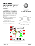
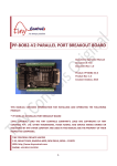
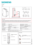
NCP2824FCT2GEVB
NCP2824FCT2 Evaluation
Board User's Manual
http://onsemi.com
EVAL BOARD USER’S MANUAL
Overview
The NCP2824 is a Filterless Class D amplifier capable of
delivering up to 2.4 W to a 4 W load with a 5 V supply
voltage. With the same battery voltage, it can deliver 1.2 W
to an 8 W load with less than 1% THD+N. The Non-clipping
function adjusts automatically the output voltage in order to
control the distortion when an excessive input is applied to
the amplifier. This adjustment is done thanks to an
Automatic Gain Control circuitry (AGC) built-in the chip.
A simple Single wire interface allows to enable/disable the
non Clipping function and also to configure the maximum
distortion level in the output. A programmable power limit
function is also embedded in order to protect speakers from
damage caused by an excessive sound level.
The intent of the evaluation boards is to illustrate typical
operation of the NCP2824 device for laboratory
characterization. The NCP2824FCT2GEVB schematic is
depicted in Figure 2.
Figure 1. NCP2824FCT2GEVB Board Picture
© Semiconductor Components Industries, LLC, 2012
May, 2012 − Rev. 2
1
Publication Order Number:
EVBUM2110/D
NCP2824FCT2GEVB
BOARD SCHEMATIC
J14CON2
2
3
100n
2
CNTL
OUTM
NCP2824
B1
Vdd
ÎÎ
ÎÎ
ÎÎ
ÎÎ
1
1
1
1
1
J10
TP 1.0D
A3
OUTP
C3
OUTN
1
1
CNTL
AGND
ÎÎ
ÎÎ
1
OUTP
INM
C2
J8
TP 1.0D
3
1
1
1
1
INP
C1
C6
4.7μF
0
1
A1
VDD
2
1
1
2
C2
INMF
0
J1
1
U1
NC
1
A2
J5
C3
4.7μF
0
1
ÎÎÎ
Î
ÎÎ
BOARD FIXATION HOLES
1
Vdd
J11
TP 1.0D
J15
2
1
2
1
CON2
SPEAKER CONNECTION
1
Jumper2
ÎÎ
ÎÎ
100μF−NC
B2
ÎÎ
ÎÎ
0
1
2
2
0
100n
1
1
1
J19
0
J9
TP 1.0D
C5
2
CUT H
J7
TP 1.0D
J2
2
C1
2
Jumper2
1
PGND
1
B3
1
2
ÎÎ
J4
1
1
J18
FIX 3.2 H FIX 3.2 H FIX 3.2 H FIX 3.2 H
CUT H
INPF
1
J17
1
2
J6
TP 1.0D
J3
1
2
ÎÎ
ÎÎ
J16
POWER SUPPLY
Jumper3
0
C4
NC
0
0
ÎÎÎÎ ÎÎ
ÎÎÎÎ ÎÎ
J12
J13
1
ENABLE− SINGLE WIRE
0
0
1
2
2
1
GND
1
TP 1.0D
0
Title
NCP2824 EVB
Size
Document Number
CustomNCP2824 EVB TLS−P−001−A−0310−DR
Date:
Figure 2. NCP2824FCT2GEVB Evaluation Board Schematic
http://onsemi.com
2
Sheet
Rev
1
of
1
NCP2824FCT2GEVB
OPERATION
The operating power supply of the NCP2824 is from 2.5
to 5.5 V. The absolute maximum input voltage is 7.0 V. A
power supply set to 3.6 V and current limit set to at least
1.5 A must be connected to J14 connector to powering the
NCP2824EVB/D. Also to compensate for parasitic
inductance of wires between the power supply and the
evaluation board it is highly recommended to connect a
470 mF electrolytic capacitor to bypass J14 terminal. Like
this the device can be evaluated under powering condition
very similar that battery power supplies.
Table 1. NCP2824 CONFIGURATION
Pulse
Counting
Register
Description
01
AGC
AGC disable
02
03
Reset
Reset configuration
04
Gain
Control
Gain = 12 dB
THD
Control
1%
05
06
Performances of EVB Solution
07
To be as close as possible with final handset application,
the design of this power conversion solution used small size
footprints where possible. Changing components may
positively or negatively impact the evaluation board
performance illustrated in Figure 3 to 8. For more
information please refer to the NCP2824 datasheet.
Single Wire Interface Operation
The single wire interface allows changing the default
configuration of the NCP2824.
After Wake up, the NCP2824 is configured with:
• AGC enable
• Non Clip + Power limit
• Gain = 18 dB
• THD max = 1%
Gain = 18 dB
2%
08
4%
09
6%
10
8%
11
10%
12
15%
13
20%
14
NC+L
Non Clip + Power limit
15
NC
Non Clip only
16
Power
Limit
Control
0.45 VPeak
17
18
The following table described all the NCP2824
configurations.
AGC Enable
0.9 VPeak
1.35 VPeak
19
1.8 VPeak
20
2.25 VPeak
21
2.7 VPeak
22
3.15 VPeak
23
3.6 VPeak
Single Wire commands can easily be emulated using a
pulse generator configured in accordance with the Single
wire specification, for more information about timings
please refers to NCP2824 datasheet.
http://onsemi.com
3
NCP2824FCT2GEVB
Table 2. BOARD CONNECTIONS
INPUT POWER
Symbol
Descriptions
J14−1
This is the positive connection for power supply. The leads (positive + ground) to the input supply should
be twisted and kept as short as possible.
J14−2
This is the return connection for the power supply (Ground signal)
J13
Ground clip
AUDIO
Descriptions
Symbol
J3
Positive Audio input
J2
Negative Audio input
J15−2
Positive Audio output
J15−1
Negative Audio output
SWITCHES SETUP
Switch Descriptions
Symbol
J1
Enable
J4
Short input capacitor on positive input
J5
Short input capacitor on negative input
J2
Connect the positive audio input to Gnd
J3
Connect the negative audio input to Gnd
TEST POINT
Switch Descriptions
Symbol
J12
This test point is directly connected to the GND
J9
This test point is directly connected to the Vdd pin
J6
This test point is connected to the positive audio input
J7
This test point is connected to the negative audio input
J10
This test point is connected to the positive audio output
J11
This test point is connected to the negative audio output
http://onsemi.com
4
NCP2824FCT2GEVB
TYPICAL OPERATING CHARACTERISTICS
THD+N vs Pout @ 255C
THD+N vs Pout @ 25°C
Vdd=2.5V
Vdd=2.7V
Vdd=3V
Vdd=3.6V
Vdd=4.2V
Vdd=5V
Vdd=5.5V
Vdd=2.5V
10
10
THD (%)
100
THD (%)
100
1
0.1
Vdd=2.7V
Vdd=3V
Vdd=3.6V
Vdd=4.2V
Vdd=5V
Vdd=5.5V
1
0.1
0.01
10
100
1000
0.01
10
10000
Pout (mW)
100
1000
10000
Pout (mW)
Figure 3. THD vs. POUT, RI = 8 W, f = 1 kHz
Figure 4. THD vs. POUT, RI = 4 W, f = 1 kHz
THD ve rsus Fre que ncy @ Vdd=3.6V
Eff vs Pout @ Vdd=3.6V
RL = 8 W
100
Pout=250mW
10
Pout=500mW
90
80
1
THD+N (%)
70
(%)
60
50
0.1
40
30
0.01
20
10
0.001
0
10
0
200
400
600
Pout (mW)
800
100
1000
1000
10000
100000
Freq (Hz)
Figure 5. Efficiency vs. POUT, RI = 8 W, f = 1 kHz
Figure 6. THD vs. Frequency, RI = 8 W,
POUT = 250 mW
PSRR vs Frequency (Inputs grounded, Gain = 12 dB, Cin = 1 mF)
P e a k vol ta ge vs. V i n for V DD= 5V
Vdd=3V
4.0
Vpeak Target=0.45V
Vpeak Target=2.25V
Vdd=3.6V
Vdd=5V
0
Temp=25 5C
Vpeak Target=0.9V
Vpeak Target=2.7V
Vpeak Target=1.35V
Vpeak Target=3.15V
Vpeak Target=1.8V
Vpeak Target=3.6V
−10
−20
3.0
−30
PSRR (dB)
3.5
(V)
2.5
2.0
−40
−50
1.5
−60
1.0
−70
0.5
0.0
0.0
−80
0.2
0.4
0.6
0.8
1.0
10
1.2
Vin(V)
100
1000
10000
Freq (Hz)
Figure 7. Peak Output Voltage in Power Limit vs. Input
Voltage (rms) and Power Limit Settings, Av = 12 dB
Figure 8. PSRR vs. Frequency
http://onsemi.com
5
100000
NCP2824FCT2GEVB
PCB LAYOUT
Figure 11 show the layout of the NCP2824FCT2GEVB
board.
For more specific layout guidelines please refer to the
NCP2824 datasheet.
As with all Class D amplifiers, care must be observed to
place the components on the PCB and layout the critical
nodes. The evaluation board is made of 4 PCB layers where
first internal layer is a GND. Figure 9, Figure 10 and
Figure 9. Assembly Layer TOP
Figure 10. Top Layer Routing
http://onsemi.com
6
NCP2824FCT2GEVB
Figure 11. Bottom Layer Routing
Table 3. BILL OF MATERIALS
Qty
Ref Des.
Description
Size
Manufacturer
Part Number
1
U1
NCP2824
CSP−9
1.45 x 1.45
mm
ON Semiconductor
NCP2824
2
C1, C2
Capacitor, Ceramic 100 nF
0603
KEMET
C0603C104K5RAC
2
C3, C6
Capacitor, Ceramic 4.7 mF 6.3 V
0603
KEMET
C0603C475K9PAC
2
J14, J15
Mal. SL5.08/2/90B plus Fem. BLZ
5.08/2
Weidmuller
SL5.08/2/90 +
BLZ 5.08/2
3
J1
Header 3 pin, 100 mil spacing
0.100 x 2
Std
Std
2
J2, J3
Header 2 pin, 100 mil spacing
0.100 x 2
Std
Std
1
J6
GND Connection
Std
Std
9
J6, J7, J9, J10,
J11, J12, J13
Test Point
Std
Std
2
J4, J5
Soldering point must be connected
1
PCB
PCB 2.0 in x 2.0 in x 1.0 mm, 4 Layers
Any
TLS−P−001−A−0310−RD
NOTE: C3 is not mounted
ON Semiconductor and
are registered trademarks of Semiconductor Components Industries, LLC (SCILLC). SCILLC reserves the right to make changes without further notice
to any products herein. SCILLC makes no warranty, representation or guarantee regarding the suitability of its products for any particular purpose, nor does SCILLC assume any liability
arising out of the application or use of any product or circuit, and specifically disclaims any and all liability, including without limitation special, consequential or incidental damages.
“Typical” parameters which may be provided in SCILLC data sheets and/or specifications can and do vary in different applications and actual performance may vary over time. All
operating parameters, including “Typicals” must be validated for each customer application by customer’s technical experts. SCILLC does not convey any license under its patent rights
nor the rights of others. SCILLC products are not designed, intended, or authorized for use as components in systems intended for surgical implant into the body, or other applications
intended to support or sustain life, or for any other application in which the failure of the SCILLC product could create a situation where personal injury or death may occur. Should
Buyer purchase or use SCILLC products for any such unintended or unauthorized application, Buyer shall indemnify and hold SCILLC and its officers, employees, subsidiaries, affiliates,
and distributors harmless against all claims, costs, damages, and expenses, and reasonable attorney fees arising out of, directly or indirectly, any claim of personal injury or death
associated with such unintended or unauthorized use, even if such claim alleges that SCILLC was negligent regarding the design or manufacture of the part. SCILLC is an Equal
Opportunity/Affirmative Action Employer. This literature is subject to all applicable copyright laws and is not for resale in any manner.
PUBLICATION ORDERING INFORMATION
LITERATURE FULFILLMENT:
Literature Distribution Center for ON Semiconductor
P.O. Box 5163, Denver, Colorado 80217 USA
Phone: 303−675−2175 or 800−344−3860 Toll Free USA/Canada
Fax: 303−675−2176 or 800−344−3867 Toll Free USA/Canada
Email: [email protected]
N. American Technical Support: 800−282−9855 Toll Free
USA/Canada
Europe, Middle East and Africa Technical Support:
Phone: 421 33 790 2910
Japan Customer Focus Center
Phone: 81−3−5817−1050
http://onsemi.com
7
ON Semiconductor Website: www.onsemi.com
Order Literature: http://www.onsemi.com/orderlit
For additional information, please contact your local
Sales Representative
EVBUM2110/D