1
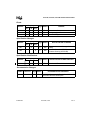
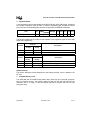
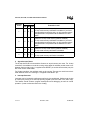
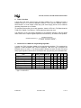
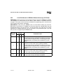
80C51GB, 83C51GB,
87C51GB
SPECIFICATION UPDATE
Release Date: December, 1996
Order Number: 272880-003
The 80C51GB, 83C51GB, 87C51GB may contain design defects or errors known as
errata. Characterized errata that may cause the 80C51GB, 83C51GB, 87C51GB’s
behavior to deviate from published specifications are documented in this specification
update.
Information in this document is provided in connection with Intel products. No license, express or implied, by
estoppel or otherwise, to any intellectual property rights is granted by this document. Except as provided in Intel’s
Terms and Conditions of Sale for such products, Intel assumes no liability whatsoever, and Intel disclaims any
express or implied warranty relating to sale and/or use of Intel products, including liability or warranties relating to
fitness for a particular purpose, merchantability, or infringement of any patent, copyright or other intellectual
property right. Intel products are not intended for use in medical, life saving, or life sustaining applications.
Intel retains the right to make changes to specifications and product descriptions at any time, without notice.
Contact your local Intel sales office or your distributor to obtain the latest specifications before placing your
product order.
*Third-party brands and names are the property of their respective owners.
Copies of documents which have an ordering number and are referenced in this document, or other Intel
literature, may be obtained from:
Intel Corporation
P.O. Box 7641
Mt. Prospect IL 60056-7641
or call in North America 1-800-879-4683, Europe 44-0-1793-431-155,
France 44-0-1793-421-777, Germany 44-0-1793-421-333, other countries 708-296-9333
Copyright © 1996, INTEL CORPORATION
ii
December, 1996
272880-003
80C51GB, 83C51GB, 87C51GB SPECIFICATION UPDATE
CONTENTS
REVISION HISTORY .................................................................................1
PREFACE ..................................................................................................2
SUMMARY TABLE OF CHANGES ...........................................................4
IDENTIFICATION INFORMATION .............................................................6
ERRATA .....................................................................................................6
SPECIFICATION CHANGES .....................................................................7
SPECIFICATION CLARIFICATIONS .......................................................13
DOCUMENTATION CHANGES ...............................................................13
272880-003
December, 1996
iii
80C51GB, 83C51GB, 87C51GB SPECIFICATION UPDATE
iv
December, 1996
272880-003
80C51GB, 83C51GB, 87C51GB SPECIFICATION UPDATE
REVISION HISTORY
Rev. Date
Version
07/01/96
001
11/13/96
002
12/11/96
003
272880-003
Description
This is the original Specification Update document. It contains all
errata identified to this date.
Deleted items from the “additions and changes to A/D converter
specifications” paragraph of erratum number 9600002 (these
items are reflected in the current version of the datasheet),
changed status of erratum number 9600002 (fixed in B-step), and
changed status of erratum number 9600003 (will be documented
in the future).
Clarified specification change number 001.
Added specification change number 002.
Added specification clarification number 001.
December, 1996
1 of 13
80C51GB, 83C51GB, 87C51GB SPECIFICATION UPDATE
PREFACE
As of July, 1996, Intel's Semiconductor Products Group has consolidated available
historical device and documentation errata into this new document type called the Specification Update. We have endeavored to include all documented errata in the consolidation
process, however, we make no representations or warranties concerning the
completeness of the Specification Update.
This document is an update to the specifications contained in the Affected
Documents/Related Documents table below. This document is a compilation of device and
documentation errata, specification clarifications and changes. It is intended for hardware
system manufacturers and software developers of applications, operating systems, or
tools.
Information types defined in Nomenclature are consolidated into the specification update
and are no longer published in other documents.
This document may also contain information that was not previously published.
Affected Documents/Related Documents
Title
Embedded Microcontrollers
MCS® 51 Microcontroller Family User’s Manual
Order
270648-008
272383-002
Nomenclature
Errata are design defects or errors. These may cause the published (component, board,
system) behavior to deviate from published specifications. Hardware and software
designed to be used with any component, board, and system must consider all errata
documented.
Specification Changes are modifications to the current published specifications. These
changes will be incorporated in any new release of the specification.
Specification Clarifications describe a specification in greater detail or further highlight
a specification’s impact to a complex design situation. These clarifications will be incorporated in any new release of the specification.
Documentation Changes include typos, errors, or omissions from the current published
specifications. These will be incorporated in any new release of the specification.
2 of 13
December, 1996
272880-003
80C51GB, 83C51GB, 87C51GB SPECIFICATION UPDATE
NOTE:
Errata remain in the specification update throughout the product’s lifecycle, or until a
particular stepping is no longer commercially available. Under these circumstances, errata
removed from the specification update are archived and available upon request. Specification changes, specification clarifications and documentation changes are removed from
the specification update when the appropriate changes are made to the appropriate
product specification or user documentation (datasheets, manuals, etc.).
272880-003
December, 1996
3 of 13
80C51GB, 83C51GB, 87C51GB SPECIFICATION UPDATE
SUMMARY TABLE OF CHANGES
The following table indicates the errata, specification changes, specification clarifications,
or documentation changes which apply to the 80C51GB, 83C51GB, 87C51GB product.
Intel may fix some of the errata in a future stepping of the component, and account for the
other outstanding issues through documentation or specification changes as noted. This
table uses the following notations:
Codes Used in Summary Table
Steps
X:
(No mark)
or (Blank box):
Errata exists in the stepping indicated. Specification Change
or Clarification that applies to this stepping.
This erratum is fixed in listed stepping or specification change
does not apply to listed stepping.
Page
(Page):
Page location of item in this document.
Status
Doc:
Fix:
Fixed:
NoFix:
Eval:
Document change or update will be implemented.
This erratum is intended to be fixed in a future step of the component.
This erratum has been previously fixed.
There are no plans to fix this erratum.
Plans to fix this erratum are under evaluation.
Row
Change bar to left of table row indicates this erratum is either
new or modified from the previous version of the document.
4 of 13
December, 1996
272880-003
80C51GB, 83C51GB, 87C51GB SPECIFICATION UPDATE
Errata
Number
9600001
9600002
9600003
Steppings
A-1
X
X
X
B
B-2
Page Status
6
6
7
X
Fixed
Fixed
Doc
ERRATA
Powerdown Current
Analog-to-digital Converter
Power Off Flag
Specification Changes
Number
Steppings
A-1
001
B
B-2
X
002
X
Page Status
5
Doc
5
Doc
SPECIFICATION CHANGES
Features Added and Changed in
B-step
Lock Bits Moved to UPROM to
Enhance Security (87C51GB)
Specification Clarifications
Number
001
Steppings
A-1
B
B-2
X
X
X
Page Status
5
Doc
SPECIFICATION CLARIFICATIONS
Port 1 and 3 Reset Values
Documentation Changes
Number
001
272880-003
Document
Page Status
Revision
272383-002
13
Doc
DOCUMENTATION CHANGES
MCS® 51 Microcontroller Family User’s Manual,
8XC51GB Hardware Description
December, 1996
5 of 13
80C51GB, 83C51GB, 87C51GB SPECIFICATION UPDATE
IDENTIFICATION INFORMATION
Markings
No special identifier. Standard 8XC51GX product marking.
ERRATA
9600001.
Powerdown Current
PROBLEM: The 87C51GB (A-1 stepping) powerdown current (Ipd) is defined as 200 µA
maximum with all output pins disconnected, crystal unconnected, EA# = Vcc, Port 0 =
Vcc, and RESET = Vss.
However, the 87C51GB exhibits high Ipd at high temperatures (+135°C). A typical
controller draws an average of 20 – 50 µA at room temperature. The cause of the high Ipd
is attributed to P624 process characteristics. Therefore, we do not specify Ipd on the A-1
stepping, so powerdown mode is restricted. We expect the problem to be resolved when
the 87C51GB (B stepping) moves to process P629.
IMPLICATION: In high-temperature environments, systems may exhibit higher than
expected Ipd.
WORKAROUND: None defined.
STATUS: Fixed. Refer to Summary Table of Changes to determine the affected steppings.
9600002.
Analog-to-digital Converter
PROBLEM: The 87C51GB (A-1 stepping) A/D channel 4 (ACH4) has been despecified.
Channel 4 does not convert correctly at combinations of high Vcc, high frequency, and low
temperature. The remaining channels (ACH0–ACH3 and ACH5–ACH7) are fully functional
at –45 to +135°C.
In the A-1 stepping, the input to the A/D converter is a field-effect transistor (FET), and
Input resistance is 1 MΩ or greater.
IMPLICATION: Designs using ACH4 at low temperature, high Vcc, and high frequency
may experience unpredictable results.
WORKAROUND: Avoid using ACH4, especially under the indicated conditions.
6 of 13
December, 1996
272880-003
80C51GB, 83C51GB, 87C51GB SPECIFICATION UPDATE
STATUS: Fixed. Refer to Summary Table of Changes to determine the affected steppings.
9600003.
Power Off Flag
PROBLEM: The power off flag (POF) is mentioned in the 87C51GB Architectural
Overview; however, it was not included in the datasheet because it is not fully tested. The
POF will be tested at Vcc=3.0V and defined in a future datasheet after the B-step.
IMPLICATION: It is unlikely that this condition will cause a system malfunction.
WORKAROUND: None.
STATUS: Doc. Refer to Summary Table of Changes to determine the affected steppings.
SPECIFICATION CHANGES
001.
Features Added and Changed in B-step
PROBLEM: The 8xC51GB (B-step) is based on the FX core, with all of the FX design
features. The B-step includes the following major changes and enhancements.
•
Changed Features
— Port 1 reset state (low after reset)
— Reset pin polarity (active low)
— Third signature byte is implemented
•
Added Features
— Third lock bit implemented
— Asynchronous reset
— Interrupts can be invoked by software (undocumented in A-step)
— P1.0/T2 is Timer 2 overflow output
— P3.3 function added for programming protection
Changed Features
This section describes the features that changed from the A-step to the B-step 87C51GB.
1.
Port 1 Reset State
Port 1 is low after reset in B-step, but was high after reset in A-step. This change makes
ports 1 and 4 at the same logic levels during reset and operation. (Only port 1 reset logic
272880-003
December, 1996
7 of 13
80C51GB, 83C51GB, 87C51GB SPECIFICATION UPDATE
level was changed.) The port 1 registers, timer functions, and timer logic levels remain the
same as in A-step.
If both A-step and B-step controllers are to be used with a common PC board, software
might be used during initialization to invert B-step port 1 outputs (write SFR 90H just after
reset) to maintain the same logic levels for A-step and B-step controllers. This action could
cause a “glitch” during reset on the B-step port 1 outputs. Unless a valid reset pulse (two
machine cycles or longer) is provided, the ports will not latch their reset state.
2.
Reset Polarity
The reset signal is active-low in B-step, but was active-high in A-step. This change allows
designers to use a simple RC circuit to reset the controller at power-up. An internal 100Ω
pullup resistor permits generating a power-on reset using only an external capacitor to
ground. The capacitance should be large enough to allow the crystal oscillator time (at
least two machine cycles) to start before the capacitor releases the reset signal. If the
reset pin is connected to ground through a 1-µF capacitor, the B-step 87C51GB will
generate an automatic reset when Vcc is turned on.
The “Power on Reset Circuitry” drawing in the 8XC51GB Hardware Description in the
MCS® 51 Microcontroller Family User’s Manual shows the capacitor connected from the
reset pin to ground.
The A-step required an inverter in the reset circuit for most regulators. The B-step does
not require the inverter. When reset is held low, the B-step 87C51GB enters the reset
state. When reset is driven high or released, the internal pullup resistor pulls the reset
signal high and allows the processor to begin executing instructions at 0000H.
Unless a valid reset pulse (two machine cycles or longer) is provided, the ports will not
latch their reset state.
If both A-step and B-step controllers are to be used with a common PC board, jumpers
should be included in the reset circuit for inverter or capacitor changes. These jumpers
shuld allow designers to configure the reset signal for A-step or B-step controllers with
little effort. If only B-step controllers are used, the reset circuit can be designed without the
jumpers.
8 of 13
December, 1996
272880-003
80C51GB, 83C51GB, 87C51GB SPECIFICATION UPDATE
3.
Signature Bytes
A new signature byte has been added to the 83C51GB and 87C51GB B-step, increasing
the number of signature bytes to three. To read the signature bytes, activate the control
pins as shown in the following table and use the procedure for EPROM verification.
Task
RST PSEN#
Read Signature Bytes
H
L
ALE/
EA#/Vpp P2.6 P2.7 P3.3 P3.6 P3.7
PROG#
H
H
L
L
L
L
L
The following tables list the locations and contents of the signature bytes for the A-step
and B-step, respectively.
Contents
Location
87C51GB
A-step
83C51GB
A-step
1EH
1FH
89H
5AH
89H
5BH
Description
Identifies the product as an Intel controller
Identifies the specific product
Contents
Location
87C51GB
B-step
83C51GB
B-step
30H
31H
60H
89H
58H
EBH
89H
58H
6BH or EBH
Description
Identifies the product as an Intel controller
Identifies an FX-core product
Identifies the specific FX-core product
Added Features
This section describes the enhancements to the B-step controller, which is based on the
FX core.
1.
Program Memory Lock
The 83C51GB and 87C51GB B-step feature three locks bits and a 64-byte encryption
array for program security. The following table lists the lock bits and their effect on the
controller. Item 5 on page 11 lists the signals required to program the lock bits and
encryption array.
272880-003
December, 1996
9 of 13
80C51GB, 83C51GB, 87C51GB SPECIFICATION UPDATE
Security
Level
Lock Bit
LB3 LB2 LB1
Protection Level
No program lock features are implemented.
On-chip code memory verification is enabled. If you have
1
U
U
U programmed an encryption array, on-chip program code is
encrypted before it is placed onto the data bus for verification.
Code executing from external memory cannot fetch code
bytes from on-chip code memory (MOVC disabled).
2
U
U
P On-chip code memory verification is enabled. If you have
programmed an encryption array, on-chip program code is
encrypted before it is placed onto the data bus for verification.
Code executing from external memory cannot fetch code
3
U
P
P bytes from on-chip code memory (MOVC disabled).
On-chip code memory verification is disabled.
Code cannot execute from external memory.
4
P
P
P
On-chip code memory verification is disabled.
U = unprogrammed; P= programmed. Other combinations of the lock bits are undefined.
2.
Asynchronous Reset
The B-step 8xC51GB microcontrollers feature an asynchronous port reset. For A-step
controllers, the oscillator must be be running and at least 19 oscillator periods must occur
between the time that a logic 1 is applied to the RESET pin and the time that the port pins
are driven to their reset states.
For B-step controllers, the oscillator need not be running. The port pins are driven to their
reset states as soon as a valid logic 1 is applied to the RESET pin.
3.
Interrupt Structure
Interrupts can be invoked by software as well as by the peripherals. Software can invoke
an interrupt by writing to an interrupt pending register (C5H and C6H in the SFR map).
This feature should enhance program development and debugging as well as normal
operation. (It was not documented in the A-step.)
10 of 13
December, 1996
272880-003
80C51GB, 83C51GB, 87C51GB SPECIFICATION UPDATE
4.
Timer 2 Clockout
A 50% duty-cycle clock output function has been added to P1.0. In addition to being a
standard I/O pin, P1.0 has two alternate functions: it can input the external clock for
timer/counter 2; or it can output a 50% duty-cycle clock ranging from 61 Hz to 4 MHz at
operating frequencies up to 16 MHz.
To configure timer/counter 2 as a clock generator, clear the C/T2 bit in T2CON and set the
T2OE bit in T2MOD. The TR2 bit in T2CON starts and stops the clock.
The frequency of the clock output depends on the oscillator frequency and the reload
value of the Timer 2 capture registers (RCAP2H and RCAP2L), as shown in this equation:
Oscillator Frequency
Clockout Frequency = ---------------------------------------------------------------------------------------4 × ( 65536 – RCAP2H, RCAP2L )
5.
Control Pin P3.3 Added to Programming Algorithm
A control pin (P3.3) has been added to the programming algorithm. This programming
algorithm is not compatible with previous steppings. Hold P3.3 high to program the
EPROM and low to verify it. The following table indicates the levels at which the control
and program signals must be held to accomplish each programming and verification task.
Task
RST PSEN#
ALE/ EA#/Vpp P2.6 P2.7 P3.3 P3.6 P3.7
PROG#
Program Code
H
L
L†
Vpp ††
Verify Code
H
L
H
H
†
Program Encryption Array H
L
L
Vpp ††
†
Program Lock Bit 1
H
L
L
Vpp ††
†
Program Lock Bit 2
H
L
L
Vpp ††
Program Lock Bit 3
H
L
L†
Vpp ††
Read Signature Bytes
H
L
H
H
† ALE/PROG# is pulsed low for 100 µs for programming.
††
Vpp = +12.5V ± 5%
272880-003
December, 1996
L
L
L
H
H
H
L
H
L
H
H
H
L
L
H
L
H
H
H
H
L
H
H
L
H
L
H
L
H
H
H
H
L
L
L
11 of 13
80C51GB, 83C51GB, 87C51GB SPECIFICATION UPDATE
002.
Lock Bits Moved to UPROM to Enhance Security (87C51GB)
PROBLEM: To enhance security, the lock bits have been moved from EPROM to UPROM.
The UPROM is a secure area on the device; values written to UPROM cannot be
changed. The function of the lock bits, the method for programming them, and the use of
the encryption array remain unchanged.
IMPLICATION: Verify that your EPROM code is correct before setting any lock bits.
Because the lock bits are in UPROM, the lock bits cannot be changed after they are
programmed once. If you set only LB1, you can still verify your code, but you cannot
reprogram the EPROM (although you can still erase it using ultraviolet light). If you set
LB2, you can no longer verify the EPROM code.
Security
Level
Lock Bit
LB3 LB2 LB1
Protection Level
No program lock features are implemented.
On-chip code memory verification is enabled. If you have
1
U
U
U programmed an encryption array, on-chip program code is
encrypted before it is placed onto the data bus for verification.
Code executing from external memory cannot fetch code
bytes from on-chip code memory (MOVC disabled).
2
U
U
P On-chip code memory verification is enabled. If you have
programmed an encryption array, on-chip program code is
encrypted before it is placed onto the data bus for verification.
Code executing from external memory cannot fetch code
3
U
P
P bytes from on-chip code memory (MOVC disabled).
On-chip code memory verification is disabled.
Code cannot execute from external memory.
4
P
P
P
On-chip code memory verification is disabled.
U = unprogrammed; P= programmed. Other combinations of the lock bits are undefined.
12 of 13
December, 1996
272880-003
80C51GB, 83C51GB, 87C51GB SPECIFICATION UPDATE
SPECIFICATION CLARIFICATIONS
001.
Port 1 and 3 Reset Values
PROBLEM: The reset value of all ports is logic “1”; however, the reset value of ports 1 and
3 is sustained by a weak pull-up. It is recommended that applications not use the reset
value of these ports to drive external loads. If the application requires the use of the reset
value of these ports, an external pull-up resistor should be added.
DOCUMENTATION CHANGES
001.
MCS® 51 Microcontroller Family User’s Manual, 8XC51GB
Hardware Description
ITEM: The 8XC51GB Hardware Description in the MCS® 51 Microcontroller Family
User’s Manual contains an error. On page 6-41, the last two sentences of Section 11.1
should read as follows:
If OSCR = 0FEH, the OFD is enabled. If OSCR=0FFH, the OFD is disabled.
272880-003
December, 1996
13 of 13