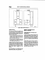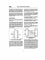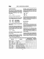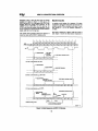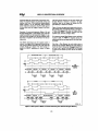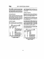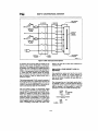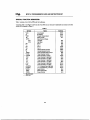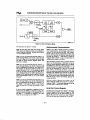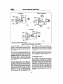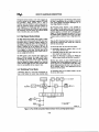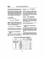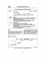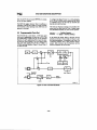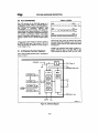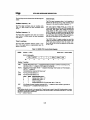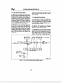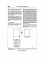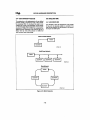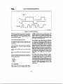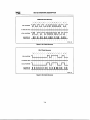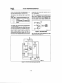
1
MCS@51 MICROCONTROLLER FAMILY USER’S MANUAL ORDER NO.: 272383-002 FEBRUARY 1994 Intel Corporation makes no warrsnfy for the uee of ite products and assumes no responsibility for any ewors which may appear in this document nor does it make a commitment to update the information contained herein. Intel retains the right to make changes to these specifications at any time, without notk Contact your local Intel sales office or your distributor to obtain the latest speoificationa before placing your product order. MDS is an ordering code only and is not usad ae a product name or trademark of Intel Corporation. Intel Corporation and Intel’s FASTPATH trademark or products, are not affiliated with Kinetics, a division of Excelan, ●Ofher brands and names are the properly of their respective owners, Additional copies of this document or other Intel literature maybe obtained from: Intel Corporation Literature Selas P.O. Box 7S41 Mt. Prospect, IL 6005S-7641 or call 1-800-879-4683 c-INTELCORPORATION, 1093 Inc. or its FASTPATH PAGE MCS” 51 CONTENTS MICROCONTROLLER c“*pTf== 1 FAMILY MCS 51 Family of Microcontrollers Archkedural Ovewiew .............................l-l USER’S MANUAL CHAPTER 2 MCS 51 Programmer’s Guide and Instruction Set ..........................................2-l CHAPTER 3 8051, 8052 and 80C51 Hardware Description ...............................................3.l CHAPTER 4 8XC52J54/58 Hardware Description ............4-1 CHAPTER 5 8XC51 FX Hardware Description .................5-1 CHAPTER 6 87C51GB Hardware Description .................8-1 CHAPTER 7 83CI 52 Hardware Description ....................7-1 MCS@ 51 Family of Microcontrollers Architectural Overview 1 MCS@51 FAMILY OF MICROCONTROLLERS ARCHITECTURAL OVERVIEW CONTENTS INTRODUCTION PAGE .........................................1-3 CHMOS Devices .....”.....’.......”.....-...-..........I-5 M;~$&:RGA-~oN INMc- 51 .................................................1-6 Lo ical Separation of Program and Data h emoy ....................................................l+ Program Memo~ .........................................l-7 Data Memory ...............................................1 -8 THE MC951 INSTRUCTION SET .............1 -9 Program Status Word ..................................1 -9 Addressing Modes .....................................l-l O Arithmetic Instructions ...............................1-10 Logical lnstrudions Data Tran#ers ....................................l.l2 ...........................................l.l2 Boolean Instructions ..................................1-14 Jump Instructions ......................................1-16 CPU TIMING .............................................l-l7 Machine Cycles .........................................1-18 Interrupt Structure ......................................l.2O ADDITIONAL 1-1 REFERENCES ...................1 -22 ir&L [email protected] ARCHITECTURAL OVERVIEW INTRODUCTION The8051 is the original member of the MCW-51 family, and is the core for allMCS-51 devices. The features of the 8051 core are ● 8-bit CPU optimized for control applications ● Extensive Boolean processing (Single-blt logic) capabtilties ● ● ● ● ● ● ● ● ● 64K Program Memory address space 64K Data Memory address space 4K bytes of on-chip Program Memory 128 bytesof on-chip Data RAM 32 bidirectional and individually addressable 1/0 lines Two 16-bit timer/counters Full duplex UART 6-source/5-vector interrupt structure with two priority levels On-chip clock oscillator The basic architectural structure of this 8051 core is shown in Figure L EXTERNAL INTERRUPTS ,, I I COUNTER INPUTS w H H II BUS CONTROL Q SERIAL PORT 4 1/0 PORTS 11 TXO Po P2 PI RXD P3 AODRESS/DATA 270251-1 Figure 1. Block Diagram of the 8051 Core 1-3 intd. MCS@-51 ARCHITECTURAL 1-4 OVERVIEW i~. MCS@’-5l ARCHITECTURAL 1-5 OVERVIEW [email protected] i~. * ----------- 8 1 1 1 1 1 1 1 I 1 ARCHITECTURAL PROORAMMrhtosv (REM ONLY) -------------$ s FFFFw T I 1 1 1 1 1 1 1 1 1 1 - I o 8 0 0 0 8 0 1 1 1 1 1 I 1 1 1 I , B I I EXTERNAL 0 9 I I I , 1 I : # G=o o 2STERNAL 0 1 0 @ * I : ● - ---------- m.1 IN7ERNAL 0000 -------- : : 0 9 * I I I -.! OVERVIEW -----------------------t 8 I 1 I 8 I I I : o # 8 9 8 8 0 0 9 t # I , 1 : FfH: OATAMEMORY (RW/WRlT2) . . . . . 8 8 I I 0 I * 0 I I # I I I I I I 1 EXIERNALm - : 1 I I IN7ERNM I 1 I 1 1 0 1 1 ------ 0: 9, e, 9 0 9 8 1 I 00 ,1+ 1 ● -------- 0000 --------- ..- J: -. 1% -.-: tiR 270251-2 Figure 2. MCW’-51 Memory Structure CHMOS Devices MEMORY ORGANIZATION MCS@-51 DEVICES Functionally, the CHMOS devices (designated with “C” in the middle of the device name) me all fiuy compatible with the 8051, but being CMOS, draw less current than an HMOS counterpart. To further exploit the power savings available in CMOS circuitry, two reduced power modes are added ● Software-invoked Idle Mode, during which the CPU is turned off while the RAM and other on-chip peripherals continue operating. In this mode, current draw is reduced to about 15% of the current drawn when the device is fully active. ● Software-invoked Power Down Mode, during which all on-chip activities are suspended. The on-chip RAM continues to hold its data. In this mode the device typically draws less than 10 pA. Logical Separation Data Memory IN of Program and AU MCS-51 devices have separate address spacea for Program and Data Memory, as shown in Figure 2. The logical separation of Program and Data Memory allows the Data Memory to be acceased by 8-bit addressea, which can be more quickly stored and manipulated by an 8-bit CPU. Nevertheless, ld-bh Data Memory addresses can also be generated through the DPTR register. Program Memory can only be read, not written to. There can be up to 64K bytes of Program Memory. In the ROM and EPROM versions of these devices the loweat 4K, 8K or 16K bytes of Program Memory are provided on-chip. Refer to Table 1 for the amount of on-chip ROM (or EPROM) on each device. In the ROMleas versions all Program Memory is external. The read strobe for external Program Memory is the signal PSEN @rogram Store Enable). Although the 80C51BH is functionally compatible with its HMOS counterpart, s~lc differeneea between the two types of devices must be considered in the design of an application circuit if one wiahea to ensure complete interchangeability between the HMOS and CHMOS devices. These considerations are discussed in the Ap plieation Note AP-252, “Designing with the 80C5lBH. For more information on the individual devices and features listed in Table 1, refer to the Hardware De scriptions and Data Sheets of the specific device. 1-6 intel. MCS@-51 ARCHITECTURAL OVERVIEW The lowest 4K (or SK or 16K) bytes of Program Memory can be either in the on-chip ROM or in an external ROM. This selection is made by strapping the ~ (External Access) pin to either VCC or Vss. Data Memory occupies a separate addrexs space from %OgrCt122 hkznory. Up to 64K bytes of exterttd RAM can be addreased in the externrd Data Memo~. The CPU generatea read and write signals RD and ~, as needed during external Data Memory accesses. In the 4K byte ROM devices, if the= pin is strapped to VcC, then program fetches to addresses 0000H through OFFFH are directed to the internal ROM. Program fetches to addresses 1000H through FFFFH are directed to external ROM. External Program Memory and external Data Memory ~~ combined if-desired by applying the ~ ~d PSEN signals to the inputs of an AND gate and using the output of the gate as the read strobe to the external Program/Data memory. ProgramMemory In the SK byte ROM devices, = = Vcc selects addresses (XtOOHthrough lFFFH to be internal, and addresses 2000H through F’FFFH to be external. Figure 3 shows a map of the lower part of the Program Memory. After reset, the CPU begins execution from location OWOH. In the 16K byte ROM devices, = = VCC selects addresses 0000H through 3FFFH to be internal, and addresses 4000H through FFFFH to be external. AS shown in F@ure 3, each interrupt is assigned a tixed location in Program Memory. The interrupt causes the CPU to jump to that location, where it commences execution of the serviee routine. External Interrupt O, for example, is assigned to location 0003H. If External Interrupt O is going to & used, its service routine must begin at location 0003H. If the interrupt is not going to be used, its service location is available as general purpose Program Memory. If the ~ pin is strapped to Vss, then all program fetches are directed to external ROM. The ROMleas parts must have this pin externally strapped to VSS to enable them to execute properly. The read strobe to externally: PSEN, is used for all external oro.cram fetches. PSEN LSnot activated for in- ‘s & ..-. (O033H) m% 1 l== 1 EPROM INSTR. Po m 002EH = ALE 002SH INTSRRUPT LOCATIONS LArcn Ssvrm 0013H II 270251-4 000SH 0003H R2S~ i AOOR a’s ‘z~ 00IBH Figure 4. Executing from External Program Memory 0000H 270251-3 Figure 3. MCW’-51 The hardware configuration for external program execution is shown in Figure 4. Note that 16 I/O lines (Ports O and 2) are dedicated to bus fictions during external Program Memory f~hes. Port O(PO in Figure 4) servex as a multiplexed address/data bus. It emits the low byte of the Program Counter (PCL) as an address, snd then goes into a float state awaiting the arrival of the code byte from the Program Memory. During the time that the low byte of the Program Counter is valid on PO, the signal ALE (Address Latch Enable) clocks this byte into an address latch. Meanwhile, Port 2 (P2 in Figure 4) emits the high byte of the Program Countex (WI-I). Then ~ strobex the EPROM and the code byte is read into the microcontroller. Program Memory The interrupt aeMce locations are spaced at 8-byte intervak 0U03H for External Interrupt O, 000BH for Tmer O, 0013H for External Interrupt 1, 00IBH for Timer 1, etc. If an interrupt service routine is short enough (as is often the case in control applications), it can reside entirely within that 8-byte interval. Longer service routinea can use a jump instruction to skip over subsequent interrupt locations, if other interrupts are in use. 1-7 MCS@-51 ARCHITECTURAL Program Memory addresses are always 16 bits wide, even though the aotual amount of Program Memory used ntSy be kSS than 64K bytes. External prOq exeoutiorssacrifices two of the 8-bit ports, PO and P2, to the fisnction of addressing the Program Memory. OVERVIEW Internal Data Memory is mapped in Figure 6. The memory space is shown divided into three bloeka, which are generally referred to as the Lower 128, the Upper 128, and SFR space. Internal Data Memory addresses are always one byte Wid%which implies an address space of only 256 bytes. However, the addressing modes for intemssl RAM ean in fact seeommodate 384 bytes, using a simple trick. Direct addresses higher than 7FH awes one memory space, and indirect addresses higher than 7FH access a different memory space. Thus Figure 6 shows the Upper 128 and SFR spaceoccupyingthe ssmeblockof addrq 80H throu~ FFH, slthoud they are physically separateentities; Data Memory Theright half of Figure 2 shows the internal and external Dats Memory spaces available to the MCS-51 user. F@ure 5 shows a hardware configuration for accessing up to 2K bytes of external RAM. The CPU in this ease is executing from internal ROM. Port O serves as a multiplexed address/data bus to the RAM, and 3 lines of Port 2 are bein~d to page the RAM. The CPU generates = and WR signals as needed during exterial WM ameases. - n BANK SELECT BRS IN 7FH 2FH SN-ACORESSASLSSPACE (S~ A~ESSES O-7F) ‘1 20H 1 1FH “{ lSH 17H ‘0{ 10H OFH 0’{ OBH 07H eo{o Ill 4 SANKSOF 8 REGIS7SRS RO-R7 RESETVALUEOF S7ACKPOIN7ER 270251-7 I 1’ I 270251-5 Figure 7. The Lower 128 Bytes of internal RAM Figure 5. Accessing External Data Memory. If the Program Memory is Internal, the Other Bits of P2 are Available as 1/0. The Imwer 128 bytes of W are present in all MCS-51 devices as mapped in F@ure 7. The lowest 32 bytes are grouped into 4 banks of 8 registers. Program instructions call out these registers as RO through R7. Two bits in the Program Status Word (PSW) seleet which register bank is in use. This allows more effieient use of code space, since register instructions are shorter than instructions that use direet addreasiig. There ean be up to 64K bytea of external Data Memory. External Data Memory addresses can be either 1 or 2 bytes wide. One-byte addresses are often used in cxmjunction with one or more other 1/0 lines to page the R4M, as shown in Figure 5. Two-byte addresws ears atso be used, irz which case the high address byte is emitted at Port 2. ~:.. .-... - , AC=IELE , SV INDIREC7 : AtORESSING ONLY SDH9 UPP~ FFH I FFH ACCESSIBLE BV OIRECT AODRSSSING EP ‘m ACCESSIBLE LOWER SY 01REC7 128 ANO INC+REC7 o AGGRESSING 80H W 1 SPWAL NC710N &oAmm~o ‘E~m CONTROLems TIMER RE— STACKiolN7ER ACCUMULATOR (’nC.) NO SIT-AOORSSSABLE SPACES AVAIUBLE AS S7ACK SPACEIN DEVICESWMI 256 BWES RAM NOT IMPLE14EN7ED IN 8051 80H 270251-6 270251-8 Figure 6. The Upper 128 Bytes of Internal RAM Figure 6. Internal Data Memory I-6 in~. M~@-51 ARCHITECTURAL CTIAC] FOIRSIIRBO[ A a a b OVI * OVERVIEW A I P I KWO 1 PARllY OFACCLWUIATORSS7 ~ NARoWARCTO 1 IF IT CONTAINS AN 000 NUMBEROF 1S, OTHERWISE 171SRESE7TO0 CARRYFLAGRECEIVESCMi/fmw; FROU BIT 1 Of ALU OPERANOS Psw6— AUXILIARYCARRYFLAG RECEIVES CARRYOUT FROM B171 OF AOOMON OPERANOS — Psw 1 USER OEFINABLEFUG nw5 GENERALPURPOSES7ATUS FLAG Psw 2 OVERFLOWFIAO SET BY ARITIMCWOPERAl!ONS REGtS7ER BANKSW’% Psw3 REOSJER BANKSELECT Bll O t 270251-10 -. .- . . . . . .- . . . ... .. . . . ------ ---- Figure 1u. Psw (Progrsm ssssus worn) Register m mc5w-51 The next 16 bytea above the register bankBform a block of bit-addressable memory apace. The MCS-51 instruction set includes a wide seleetion of single-blt instructions, and the 128 bits in this area can be directly addressed by these irsstmctions. The bit addreascs in this area are W)H through 7FH. t2evtces !%teers addresses in SFR mace are both byte. and bit. addressable. The blt-addre&able SFRS are ‘those whose address ends in 000B. The bit addresses in this ares are 80H throUgh FFH. THE MCS@-51 INSTRUCTION All of the bytes in the LQwer 128 can be accessed by either direct or indirect addressing. The Upper 128 (Figure 8) can only be accessed by indirect addressing. The Upper 128 bytes of RAM are not implemented in the 8051, but me in the devices with 256 bytea of RAM. (Se Table 1). All members of the MCS-51 family execute the same instruction set. The MCS-51 instruction set is optimized for 8-bit control applications. It provides a variety of fast addressing modes for accessing the internal MM to facilitate byte operations on small data structures. The instruction sd provides extensive support for one-bit variables as a separate data t% allowing direct blt manipulation in control and logic systems that require Boolean prmessirsg. Figure 9 gives a brief look at the Special Funotion Register (SFR) space. SFRS include the Port latchea, timers, pe2iphA controls, etc. l%ese registers can only& -seal by dmect addressing. In general, all MCS-51 microcontrollers have the same SFRB as the 8051, and at the same addresses in SFR space. However, enhancements to the 8051 have additional SFRB that are not present in the 8051, nor perhaps in other proliferations of the family. “u RE~MAPPSO An overview of the MCS-51 instruction set is prrsented below, with a brief description of how certain instructions might be used. References to “the assembler” in this discussion are to Intel’sMCS-51 Macro Assembler, ASM51. More detailed information on the instruction set can be found in the MCS-51 Macro Assembler User’s Guide (Grder No. 9W3937 for 1S1SSystems, Grder No. 122752 for DOS Systems). POR7S EOH Program Status Word AOORESSES7NAT END IN OH OR EN ARCALSO B~-AOORESSABLE m The Program Status Word (PSW) contains several status bits that reflect the current state of the CPU. The PSW, shown in Figure 10, resides in SFR space. It contains the Csrry bi~ the Auxdiary Carry (for BCD operations), the two register bank select bits, the Gvesflow flag, a Parity bit, and two userdefinable status tlags. PORT .3 80H AOH Porn 2 90H POR7 1 SET -POR7 PINS -ACCUMULATOR -Psw (E7c.) B The Carry bit, other than serving the functions of a Carry bit in arithmetic operations, also sesws as the “Accumulator” for a number of Boolean operations. J-A--I 270251-9 Figure 9. SFR Spsce 1-9 MCS@-51 ARCHITECTURAL The bits RSOand RSl are wed to select one of the four register banks shown in Figure 7. A number of instructions refer to these RAM locations as RO through R7. The selection of which of the four banks is being referred to is made on the basis of the bits RSO and RS1 at execution time. The Parity bit reflects the number of 1s in the Accumulator P = 1 if the Accumulator contains an odd number of 1s, and P = O if the Accumulator contains an even number of 1s. Thus the number of 1s in the Accumulator plus P is always even. Two bits in the PSW are uncommitted and maybe used as general purpose status flags. Addressing Modes The addressing modes in the MCS-51 instruction set are as follows OVERVIEW IMMEDIATE CONSTANTS The value of a constant can follow the opcode in Program Memory. For example, MOV A, # 100 loads the Accumulator with the decimal number 100. The same number could be specified in hex digitz as 64H. INDEXED ADDRESSING only Program Memory can be amessed with indexed addressing, and it can only be read. This addressing mode is intended for reading look-up tables in Program Memory. A Id-bit base register (either DPTR or the Program Counter) points to the base of the table, and the Accumulator is setup with the table entry number. The address of the table entry in Program Memory is formed by adding the Accumulator data to the base pointer. DIRECT ADDRESSING In direct addressing the operand is specitied by an 8-bit addreas field in the instruction. Only internal Data RAM and SFRS can be directly addressed. INDIRECT ADDRESSING In indirect addressing the instruction specifies a register which contains the address of the operand. Both internal and external RAM can be indirectly addressed. The address register for 8-bit addresses can be RO or RI of the selected register bank, or the Stack Pointer. The addreas register for id-bit addresses can only be the id-bit “data pointer” register, DPTR. REGISTER Another type of indexed addreaaing is used in the “case jump” instruction. In this case the destination address of a jump instruction is computed as the sum of the base pointer and the Accumulator &ta. Arithmetic Themenu of arithmetic instructions is listed in Table 2. The table indicates the addressing modes that can be used with each instruction to access the <byte> operand. For example, the ADD A, <byte> instruction can be written as ADD ADD ADD ADD INSTRUCTIONS The register banks, containing registers RO through R7, can be accemed by certain instructions which carry a 3-bit register specification within the opcode of the instruction. Instructions that access the registers this way are code efficient, since this mode elirninatez an addreas byte. When the instruction is executedj one of the eight registers in the selected bank is amessed. One of four banks is selected at execution time by the two bank select bits in the PSW. REGISTER-SPECIFIC INSTRUCTIONS Some instructions are specific to a certain register. For example, some instructions always operate on the Accumulator, or Data Pointer, etc., so no address byte is Inneeded to point to it. The opcode itself does that. structions that refer to the Accurrdator as A assemble as accumulator-specific opcmdes. Instructions A,7FH A,@RO A,R7 A, # 127 (direct addressing) (indirect addressing) (register addressing) (iediate constant) The execution times listed in Table 2 assume a 12 MHz clock frequency. All of the arithmetic instructions execute in 1 ps except the INC DPTR instruction, which takes 2 W, snd the Multiply and Divide instructions, which take 4 ps. Note that any byte in the internal Data Memory space can be incremented or decremented without going through the Accumulator. One of the INC instructions operates on the Id-bit Data Pointer. The Data Pointer is used to generate 16-bit addresses for external memory, w being able to increment it in one 16-bit operation is a usefirl feature. The MUL AB instruction multiplies the Accumulator by the data in the B register and puts the Id-bit product into the concatenated B and Accumulator registers. 1-1o inl# MCS@-51 ARCHITECTURAL OVERVIEW Table 2 A Ust of the MCS@I-51 Arithmetic Mnemonic Addressing Operation Dk ADD I I A, <byte> ADDOA, <byte> SUBB A, <byte> INC A INC . <byte> A = A + I A= A+< A–<byte>-C I A=A+l I <byte> I Ind byte>+C I X I X x lmm x I 1 x X x I =<byte>+l Execution Time (@ Modes Rq x x <byte> A= Instructions I X ] X I X I X I 1 11-1 I I lhJC DPTR I DPTR = DpTR + 1 I Data Pointer only 121 I DEC A I A= A-l I Accumulator only Ill DEC <byte> <byte> MUL AB B.A=Bx DIV AB I IDAA = <byte> x – 1 x I A I A = Int [A/B] B = MOd [A/Bl I Decimal Adjust I The DIV AB instruction divides the Accumulator by the data in the B register and leevea the 8-bit quotient in the Accumulator, and the 8-bit remainder in the B register. x 1 I ACC and B only ACC and B only I 1 Accumulator onlv I 1 x x 4 I I 4 Ill Accumulatoronly eompletcs the shift in 4 p.s and leaves the B register holding the bits that were shifted out. The DA A instruction is for BCD arithmetic operations. In BCD arithmetic, ADD and ADDC instructions should always be followed by a DA A operation, is also in BCD. Note that DA to ensure that the red A will not convert a binary number to BCD. The DA A operation produces a meaningfid result only as the second step in the addition of two BCD bytes. Oddly enough, DIV AB finds lees use in arithmetic “divide” routines than in radix eonversions and pro~ble shift operstioILs. k example of the use of DIV AB in a radix conversion will be given later. In s~ operations, dividing a number by 2n shifts its n bits to the right. Using DIV AS to perform the division Table 3. A Uet of the MCS@J-51Logical Instructions I I Mnemonic ANL A,< byte> ANL <byte>,A ANL <bvte>, A = A ORL A,< byte> ORL <bvte>,A #data ORL <byte>, #data XRL A,< byte> XRL <byte>,A XRL <byte>, .AND. <byte> <byte> = <byte> .AND. A <byte> = <byte> .AND. #data I A= A.OR. <byte> <byte> = <byte> .OR. A I <byte> = <byte> .OR. #data A = A .XOR. <byte> I #data Addressing Operation <byte> = <byte> .XOR. A <byte> = <byte> .XOR. #data Dir Ind x x x Execution Modes I Reg I Time Imm x x 1 1 2 x I X1X1X1X x x X1X1X x I I (ps) X 1 1 2 x 1 I 1 2 I CRL A A=OOH Accumulator only 1 CPL A A = Accumulator only 1 IRL RLC .NOT. A A I Rotate ACC Left 1 bit A I Rotate Left through Csrry Rotate ACC Right 1 bit RR A RRC A Rotate SWAP A Swap Nibbles in A Right through Carry 1-11 I I Accumulator onlv Ill I Accumulator only I 1 Accumulator only 1 Accumulator only 1 Accumulator onlv 1 I irrtel. MCS@-51 ARCHITECTURAL The SWAP A instruction interchanges the high and low nibbles within the Accumulator. This is a useful operation in BCD manipulations. For exampie+ if the Accumulator contains a binary number which is known to be leas thsn IQ it can be qnickly converted to BCD by the following code: Logical Instructions Table 3 shows the list ofMCS-51 logical instructions. The instructions that perform Boolean operations (AND, OIL Exclusive OIL NOT) on bytes perform the operation on a bit-by-bit bssis. That is, if the AecumuIator contains 001101OIB and <byte> contains O1OIOOIIB,then ANL OVERVIEW MOV DIV SWAP ADD A, <byte> B,# 10 AB A A,B will leave the Accumulator holding OOO1OOOIB. Dividing the number by 10 leaves the tens digit in the low nibble of the Accumulator, and the ones digit in the B register. The SWAP and ADD instructions move the tens digit to the high nibble of the Accumulator, and the onea digit to the low nibble. The addrcasing modes that can be used to access the <byte> operand are listedin Table 3. Thus, the ANL A, <byte> instruction may take any of the forms ANL ANL ANL ANL A,7FH A,@Rl A,R6 A, # 53H (direct addressing) (indirect addressing) (register addressing) (immediate constant) Data Transfers INTERNAL AU of the logical instructions that are Accumulatorspecflc execute in lps (using a 12 MHz clock). The othem take 2 ps. Note that Boolean operations can be performed on any byte in the lower 128 internal Data Memory space or the SFR space using direct addressing, without having to use the Accumulator. The XRL <byte >, #data instruction, for example offets a quick and easy way to invert port bits, as in XRL Pl,#oFFH If the operation is in response to an interrupt, not using the Accumulator saves the time and effort to stack it in the service routine. The Rotate instructions (3U & RLC A, etc.) shift the Aeeurtmlator 1 bit to the MI or right. For a left rotation, the MSB rolls into the LSB position. For a right rotation, the LSB rolls into the MSB position. Table 4. A List of the MCS@-51 Data Tranafer Mnemonic RAM Table 4 shows the menu of instructions that are available for moving data around within the internal memory spaces, and the addressing modes that can be used with each one. Wkh a 12 MHz clock, all of these instructions execute in either 1 or 2 ps. The MOV < dest >, < src > instruction allows dats to be transferred between any two internal RAM or SFR lwations without going through the Accumulator. Remember the Upper 128 byes of data RAM can be acwased only by indirect addressing, and SFR space only by direct addressing. Note that in all MCS-51 devices, the stack resides in on-chip RAM, and grows upwards. The PUSH instruction first increments the Stack Pointer (SP), then copies the byte into the stack. PUSH and POP use only dkcct addressing to identify the byte being saved or restored, Instructions that Access Internal Data Memory Space Addressing Operation Modes Ind Reg Imm x 1 x 2 x 2 MOV A, <src> A = <src> x x x MOV <cleat> ,A <dest> = A x x x <dest> = <src> x x x MOV <dest>, MOV DPTR,#data16 <src> DPTR = 16-bit immediate constant. PUSH <WC> INC SP: MOV “@’SP’, <src> x POP <dest> MOV <dest>, “@SP”: DEC SP x XCH A, <byte> ACC and <byte> exchange data x XCHD A,@Ri ACC and @Riexchange low nibbles 1-12 Execution Time (ps) Dir 1 2 2 x x x 1 1 i~o MCS@-51 OVERVIEW ARCHITECTURAL but the stack itself is accessed by indirect addressing using the SP register. This means the stack can go into the Upper 128, if they are implemented, but not into SFR space. Atler the routine has been executed, the Accumulator contains the two digits that were shitled out on the right. Doing the routine with direct MOVS uses 14 code bytes and 9 ps of execution time (assuming a 12 MHs clock). The same operation with XCHS uses less code and executes almost twice as fast. In devices that do not implement the Upper 128, if the SP points to the Upper 128, PUSHed bytes are lost, and POPped bytes are indeterminate. To right-shift by an odd number of digits, a one-digit shift must be executed. Figure 12 shows a sample of code that will right-shii a BCD number one digi~ using the XCHD instruction. Again, the contents of the registers holding the number and of the Accumulator are shownalongsideeachinstruction. The Data Transfer instructions include a id-bit MOV that can be used to initialise the Data Pointer (DPTR) for look-up tables in Program Memory, or for Id-bit external Data Memory accesw. The XCH A, <byte> instruction causes the Amulator snd addressed byte to exchsnge data. The XCHD A, @Ri instruction is similar, but only the low nibbles are involved in the exchange. MOV MOV Rl, #2EH RO,#2DH m loop for R1 = 2EH To see how XCH and XCHD can be used to fatitate data manipulations, consider first the problem of shit%ing an 8digit BCD number two digits to the right. Figure 11 shows how this can be done using direct MOVS, and for comparison how it can be done using XCH instructions. To aid in understanding how the code works, the contents of the registers that are holding the BCD number and the content of the Accumulator are shown alongside each instruction to indicate their status after the instruction has been executed. .00P MOV XCHD SWAP MOV DEC DEC CJNE Imp for RI = 2DH loop for R1 = 2CH: ioop for RI = 2BH: CLR XCH n3JMm MOV A,2EH MOV 2EH2DH % ;; MOV 00 12 2CH:2BH : % ~ A A,2AH 00 12 34 56 78 00 12 34 56 78 00 12 34 58 78 00 12 34 58 67 00 12 34 58 67 00 12 34 56 67 76 76 67 67 67 67 00 12 36 45 67 00 18 23 45 67 0s 01 22 45 67 45 23 01 06 01 23 45 67 00 01 23 45 67 00 06 Figure 12. Shifting a SCD Number One Digit to the Right First, pointers RI and RO are setup to point to the two bytea containing the last four BCD digits. Then a loop is executed which leaves the last byte, location 2EIL holding the last two digits of the shifted number. The pointers are decrernented, and the loop is repeated for location 2DH. The CJNE instruction (Compare and Jump if Not Equal) is a loop control that will be described later. gm (a) Using direct MOVS 14 bytes, 9 ps ~ A,@Rl A,@RO A @Rl,A RI RO Rl,#2AH,LOOP The loop is executed from LOOP to CJNE for R1 = 2EH, 2DH, 2CH and 2BH. At that point the digit that was originally shii out on the right has propagated to location 2AH. Siice that location should be left with 0s, the lost digit is moved to the Accumulator. (b) Using XCHS 9 bytes, 5 ps .. Figure 11. Shifting a BCD Number Two Dlgite to the Right 1-13 [email protected] EXTERNAL ARCHITECTURAL Alf of these instructions execute in 2 pa, with a 12 MHz clock. Tabfe 5. A List of the MCS@-51 Data Mnemonic Operation PC) - 1 The first MOVC instruction in Table 6 can accommodate a table of up to 256 entries, numbered O through 255. The number of the desired entry is loaded into the Accumulator, and the Data Pointer is setup to point to beginning of the table. Then A,@A+DPTR copies the desired table entry into the Accumulator. Execution Time (*) 8 b~ MOVX A,@’Ri Read external RAM @Ri 8 bb MOVX @Ri,A Write external RAM @Ri 2 16 bfia at (A + I MOVC Trsnafer Instructions that Accees Extarnsl Data Memory Spaoe ‘6 bns Table 6. Tha MCS3’-51 Lookup Table Read Inetmctions RAM Table 5 shows a list of the Data Transfer inatmctions that acceas external Data Memory. Only indirect ad&easing can be used. The choice is whether to use a one-byte address, @M where Ri can be either RO or RI of the selected register bank, or a two-byte address, @DPTR. The disadvantage to using 16-bit addresses if only a few K bytesof externalRAMare involvedis that 16-bit addresses use alf 8 bits of Port 2 as addreas bus. On the other hand, S-bit addresses allow one to address a few K bytes of RAM, as shown in Figure 5, without having to sacrifice all of Port 2. Address Width OVERVIEW The other MOVC instruction works the same way, except the Program Counter (PC) is used as the table base, and the table is accewed through a subroutine. First the number of the desired entry is loaded into the Accumulator, and the subroutine is cslled: ~ ‘ovx “@DpTR Read external RAM @DPTR 2 ‘ovx ‘DmR’A Writa exlemal RAM @DPTR 2 MOV CALL &ENTRY_NUMBER TABLE The subroutine “TABLE” would look like this: TABLE: Note that in all external Data RAM acaases, the Accumulator is always either the destination or source of the data. MOVC A,@A + PC The table itself immediately follows the RET (return) instruction in Program Memory. This type of table can have up to 255 entries, numbered 1 through 255. Number O can not be used, because at the time the MOVC instruction is executed, the PC contains the address of the RET instruction. An entry numbered O would be the RET opcode itseff. The read and write strobes to external RAM are activated only during the execution of a MOVX instruction. Normally these signals are inactive and in fact if they’re not going to be used at u their pins are available as extra 1/0 lines. More about that later. LOOKUP TABLES Boolean Instructions Table 6 shows the two instructions that are available for reading lookup tables in Program Memory. Since these instructions access only Program Memory, the lookup tablea can only be read, not updated. The nmemonic is MOVC for “move constant”. MCS-51 devices contain a complete Boolean (single-bit) processor. The internal RAM contains 128 addressable bits, and the SFR space can support up to 128 other addressable blta. Afl of the port lines are bWaddressabl% and each one csn be treated as a separate singleblt port. The instructions that access these bits are not just conditional branches, but a complete menu of move, aeL clear, complement, OR and AND instmctions. These kinds of bit operations are not essily obtained in other architectures with any amount of byteOriented Sottware. If the table access is to external Program Memory, then the read strobe is PSEN. 1-14 intd. MCS@-51 ARCHITECTURAL Note that the Boolean instruction set includes ANL and ORL operations, but not the XRL (_ExclusiveOR) operation. An XRL operation is simple to implement in sof?.ware.Suppose, for example, it is Wuired @ form the Exclusive OR of two bits Table 7. A List of the MCS’@-51 Boolean Instrutilons Mnemonic Operation Execution Time (us) ANL C,bit I 2 ANL C./bit !IC = C .AND. .NOT. bit I1 2 n 2 nnl F MO\ MO\ G. IC = C .AND. bit 16= C.OR. bit OVERVIEW C = bitl .XRL. bit2 The sot%vare to do that could be as follows: MOV UIL,U I UIL – w 1= I ICLR c Ic=o 1 CLR bit ]bit=o 1 Ic=l SETB bn Ibit= 1 1 CPL C I C = .NOT. C 1 CPL bit I bit = .NOT. bit 1 JC rel lJumpif C= 1 2 JNC rel Jump if C = O 2 2 JB bit,rel Jump if bti = 1 JNB bit,rel Jump if bit = O JBC bit,rel IJump if bti = 1; CLR bit I 1 This code uses the JNB instruction, one of a series of bk-teat instructions which execute a jump if the addressed bit is set (JC, JB, JBC) or if the addressed bit is not set (JNG JNB). In the above case, blt2 is being tested, and if bitZ = Othe CPL C instruction is jumped over. 2 2 JBC executes the jump if the addressed bit is set, and also clears the bit. Thus a fig can be teated and cleared in one operation. The instruction set for the Boolean processor is shown in Table 7. Alt bit ameaaca are by direct addressing. Blt addreases OOHthrough 7PH are in the Lower 128, and bit addresses 80H through FFH are in SFR space. All the PSW bits are directly addressable so the Parity bit, or the general purpose flags, for example, are also available to the bit-test instructions. Note how easily an internal ilag can be moved to a port pin: MOV MOV CPL (continue) Fkst, bit 1 is moved to the Carry. If bit2 = O, then C now contains the correct reauh. That is, bit 1 .XRL. bit2 = bitl ifbiti = O. On the other hand, ifbit2 = 1 C now contains the complement of the correct result. It need only be inverted (CPL C) to complete the opcrstion. 1 SETB C I OVER C,bit 1 bit2,0VER C RELATIVE C,PLAG P1.o,c OFFSET The destination address for these jumps is specitied to In this example, FLAG is the name of any addressable bit in the Lower 128 or SFR space. An 1/0 line (the LSB of Port 1, in this case) is set or cleared depending on whether the flag blt is 1 or O. in the PsW isused as the single-bit ACCU. The bTy bit mulator of the Boolean processor. Bit instructions that refer to the Carry bit as C assemble as Carry-specflc instructions (CLR C, etc). The Carry bit also has a direct addreas, since it resides in the PSW register, which is bit-addressable. the assembler by a label or by an actual address in Program Memory. However, the destination address assembles to a relative offset byte. This is a signed (two’s complement) oftket byte which is added to the PC in two’s complement arithmetic if the jump is executed. 1-15 The range of the jump is therefore -128 to + 127 Program Memory bytes relative to the first byte following the instruction. i~. MCS@-51 ARCHITECTURAL the Accumulator. Typically, DPTR is set up with the addms of a jump table, and the Accumulator is given an index to the table. In a 5-way branch, for examplq an integer Othrough 4 is loaded into the Accumulator. The code to be executed might be ax follows Jump lnstruMlons Table 8 shows the list of unconditional jumps. Table 8. Unconditional Jumps in MCW’-51 Oavices I Mnarnonic I JMP JMP CALL addr I I Jumo to addr @A+ DPTR I Jump to A+ DPTR addr I Return fromsubroutine I RETI I NOP 121 I DPTR, #JUMP_TABLE A,INDEX_NUMBER @A+DPTR 2 The RL A instruction converts the index number (O through 4) to an even number on the range Othrough 8, because each entry in the jump table is 2 bytee long: 2 I Call subroutine at addr 1RET MOV MOV RLA JMP Exeeution Tilna (us) Operation OVERVIEW I z I Returnfrominterrupt I 2 I No oparation 1 ~P_TABLE MMP AJMP AJMP AJMP The Table lists a single “JMP addr” instruction, but in fact there are three-SJMP, LJMP and AMP-which differ in the format of the destination address. JMP is a generic mnemonic which can be used if the programmer does not care which way the jump is eneoded. CASE_O CASE_l CASE_2 CASE_3 CASE_4 Table 8 shows a single “CALL addr” instruction, but there are two of them-LCALL and ACALL-which differ in the format in which the subroutine address is given to the CPU. CALL is a generic mnemonic which ean be used if the programmer does not care which way the address is encoded. The SJMP instruction eneodes the destination address as a relative offset, as deaeribed above. The instruction is 2 bytes long, eonsiating of the opeode and the relative offset byte. The jump distance is limited to a range of -128 to + 127 bytes reIative to the instruction following the SJMP. The LCALL instruction uses the Id-bit address format, and the subroutine ean be anywhere in the 64K Program Memory space. The ACALL instruction uses the 1l-bit format, and the subroutine most be in the same 2K bkxk as the instruction following the ACALL. The LJMP instruction eneodea the destination address as a Id-bit constant. The instruction is 3 bytes long, consisting of the opeode and two address bytes. The destination address ean be anywhere in the 64K Program Memory SPSW. The AJMP instruction encodes the destination address as an 1l-bit constant. The instruction is 2 bytee long, eonaisting of the opode, which itself contains 3 of the 11 address bits, followed by another byte containing the low 8 bits of the destination address. When the instruction is executed, these 11 bits are simply substituted for the low 11 bits in the PC. The high 5 bits stay the same. Hence the destination has to be within the same 2K block as the instruction following the AJMP. In all eases the programmer specifies the de&nation address to the assembler in the same way as a label or as a id-bit constant. The assembler will put the destination address into the eormct format for the given instruction. If the format required by the instruction will not support the distance to the specified destination rtddresa, a “Destination out of range” message is written into the Lkt fde. The JMP @A+ DPTR instruction supports ease jumps. The destination address is computed at exeeution time as the sum of the lti-bit DPTR register and 1-16 In any case the programmer specifies the subroutine address to the assembler in the same way as a label or as a 16-bit constant. The assembler will put the address into the correct format for the given instructions. Subroutines should end with a RET instruction, which returns execution to the instruction following the CALL. RETI is used to return from an interrupt service routine. The only difference between RET and RETI is that RETI tells the interrupt control system that the interrupt in progress is done. If there is no interrupt in progress at the time RETI is executed, then the RETI is functionally identical to RBT. Table 9 shows the list of conditional jumps available to the MCS-51 user. All of these jumps specify the destination address by the relative ot%et meth~ and so are lindted to a jump distance of – 128 to + 127 bytes from the instruction following the conditional jump instruction. Important to note, however, the user speeifies to the assembler the actual destination address the same way as the other jump as a label or a id-bit constant. i~. MCS@-51 ARCHITECTURAL Table 9. Conditions Mnemonic OVERVIEW Jumps in MCS@-51 Devioes Addressing Operation Dir ind Modes Rag imm Execution Time (ps) JZ rei Jump if A = O Accumulator oniy 2 JNZ rel Jumpif Accumulator oniy 2 ,rel A+O CJNE A, <byte> ,rei Deorement and jump if not zero Jumpif A # <byte> CJNE <byte> ,#data,rei Jump if <byte> # #data DJNZ <byte> There is no Zero bit in the PSW. The JZ and JNZ instructions test the Accumulator data for thst ccmdition. The DJNZ instruction (Dezrement and Jump if Not Zero) is for loop control. To execute a loop N times, load a counter byte with N and tersninate the loop with a DJNZ to the beginning of the loop, as shown below for N = 10: x x x 2 2 2 x x x @ Mes-51 HIAOS ORCHMOS ‘4-J -4-I -i-l OUART&&~WA; > STAL7. Cl RrsONAmR 57. S-TAL1 Vss = LOOP: 270251-11 MOV com~#lo (begin loop) Figure 13. Using the On-Chip Oeciilator ● * w’% (;d Imp) DJNZ COUNTER,LOOP (continue) HMOS ORCnuos SmLS The CJNE instruction (Compare and Jump if Not Equal) can also be used for loop control as in Figure 12. Two bytes are specified in the operand field of the instruction. The jump is executed only if the two bytes are not equal. In the example of Figure 12, the two bytes were the data in R1 and the constant 2AH. The initial data in R1 was 2EH. Every time the loop was executed, R 1 was decresnertted, and the looping was to continue until the R1 &ta reached 2AH. Another application of this instruction is in “great= than, less than” comparisons. The two bytes in the op erand field are taken as unsigned integers. If the first is less than the second, then the Carry bit is set (l). If the first is greater than or equal to the second, then the Carry bit is cleared. CLOCK SIGNAL STAL1 = 270251-12 A. HMOS or CHMOS Mcs”-51 EilSRNAL CLOCK HMOS ONLY STAL2 STAL1 Vss = 270251-13 B. HMOS Only CPU TIMING u Mm%! CHMOS ONLY All MCS-51 microcontrollers have an on-chip oscillator which can be used if desired as the clock source for the CPU. To use the on-chip oscillator, connect a crystal or ceramic resonator between the XTAL1 and XTAL2 pins of the microcontroller, and capacitors to ground as shown in Figure 13. (w) WRNAL STU.2 nut L= Vss s 270251-14 C. CHMOS only Figure 14. Using an Externai Ciock 1-17 i~. MCS’5’-51 ARCHITECTURAL Examples of how to drive the clock with an external oscillator are shown in Figure 14. Note that in the HMOS devices (S051, etc.) the signal at the XTAL2 pin actually drives the internal clock generator. In the CHMOS devices (SOC5lBH, ete.) the signsl at the XTAL1 pin drives the internal clock generator. If only one pin is going to be driven with the external oscillator signal, make sure it is the right pin. Machine Cycles A machine cycle consists of a sequence of 6 statea, numbered S1 through S6. Each state time lasts for two oscillator periods. Thus a machine cycle takes 12 Oscillator periods or 1 ps if the oscillator frequency is 12 MHz. Each state is divided into a Phase 1 half and a Phase 2 half. Figure 15 shows the fetch/execute sequences in The internal clock generator defmea the sequence of states that make up the MCS-51 machine cycle. 51 52 as se Plm Prps PIP2 PIPS (%L) as PIPs OVERVIEW .% Pips s as 52 PIPS Pips L as S4.SE mm PIP2 P2 PIPS I 51 Pips I ALE 1 ! I I I - nw OPCODE. J I READ NEXT :,,-4ir-NEmo”oOEAGA ~ I I (A)t-byts, l-eydshs2mdh, e.g., WC A. I I I I r I I READ OPCODE. I I I (B)2-byte. 1* lm@s2b. I i *.e.. Aoo A,mdma I I I 1 READ NEXT OPCODE OPCOOE I (DISCARD). I I [ ------S1 ------- as es e4ae imhlesm , 1 Seslases I [c) l-byle,2qs4C I AGAIN. ~ e4aEes I I ---------- RSAO NEXT OPCODE AGAIN. I , ‘1=”” I ? 1~ sla2a2s4] - as AOOR [0) MOW (l-, I I — READ OPCOOE (MWX). READ NEXT OPCOOE (OISCARD) I S-c@@ I -----I I ●.s., INC DPTR. jI----- NO eel I NO FETCH. ~NOALE 1 S11S21S2]24SSSS I ----- ,,; .----- I DATA J ACCESS EXTERNAL MEMORY I I 270251-15 Figure 15. Stete Sequences 1-18 in MCS@’-5l Devices in~e MCS@-51 ARCHITECTURAL OVERVIEW fetch/execute sequences are the same whether the Program Memory is internal or external to the chip. Execution times do not depend on whether the Program Memory is internal or external. states and phases for various kinds of instructions. NormalIy two program fetches sre generated during each machine cycle, even if the instruction being executed doesn’t require it. If the instruction being executed doesn’t need more code bytes, the CPU simply ignores the extra fetch, and the Program Counter is not incremented. The Figure 16 shows the signals and timing involved in program fetches when the Program Memory is external. If Program Memo~xternsl, then the Program Memory read strobe PSEN is normally activated twice per machine cycle, as shown in Figure 16(A). Execution of a one-cycle instruction (Figure 15A and B) begins during State 1 of the machine cycle when the opcode is latched into the Instruction Register. A second fetch occurs during S4 of the same machine cycle, Execution is complete at the end of State 6 of this mschine cycle. If an access to external Data Memory occurs, as shown in Figure 16(B), two PSENS are skippe$ because the address and data bus are being used for the Data Memory access. instructions take two machine cycles to execute. No program fetch is generated during the see ond cycle of a MOVX instruction. This is the ordy time program fetches are skipped. The fetch/execute sequence for MOVX instructions is shown in Figure 15(D). The MOVX r ONE MACHINE CVCLS sl[a21s21s41aslss ALE -N ~ SIIS21S21S41SE T I I I 1 I I 1 I I I I 1 1 P2 PCH ONE MACIUNE CYCLE I 1 ro Note that a Data Memory bus cycle takes twice as much time as a Program Memory bus cycle. Figure 16 shows the relative timing of the addresses being emitted at Ports Oand 2, and of ALE and PSEN. ALE is used to latch the low address bvte from PO into the address latch. r x [ 1 126 I I PCH OUT I x’ I ! , 1 1 1 I 1 I 1 1 I 1 PCH OUT OUTX L 1 I I I 1 I I I PCNOUT 1 I t5i:F t~::$m WITH%)UT A MOVX. ty;LL&T &T G:v:m’lxm:m -N ) I I I I ~ 1 1 I E P2PcHc@( I ! PCHOUT t P&m&T 1 1 I I OPH OUT OR P2 OUT I I I I x! , I x: I 1 1 I I I 1 PCH OUT (B) WITH A MOVX. )( PWOUT iAC:O&UT 2702!31 -16 Figure 16. Bus Cycles in MCS@-51 Oevices Extilng 1-19 irom External Program Memory i~e MCS@-51 ARCHITECTURAL When the CPU is executing from intemrd Program Memory, ~ is not activated, and program addresses are not emitted. However, ALE continues to be activated twice per machine cycle and so is available as a clock output signal. Note, however, that one ALE is skipprd during the execution of the MOVX instmction. Interrupt Structure The 8051 core provides 5 interrupt sources 2 external interrupts, 2 timer interrupts, and the serial pat interrupt. What follows is an overview of the interrupt structure for the t3051.Other MCS-51 devices have additional interrupt sources and vectors as shown in Table 1. Refer to the appropriate chapters on other devices for further information on their interrupts. INTERRUPT ENABLES Each of the interrupt sources can be individually enabled or disabled by setting or clearing a bit in the SFR (MSB) (LSB) EAl — I—IESIETI Enablebk = 1 enablesb Ensblebk =odieabksit symbol Pmiti9n EA IE.7 IEXIIETOIEXO OVERVIEW natned IE (Interrupt Enable). This register also contains a global disable bit, which can be cleared to disable all interrupts at once. Figure 17 shows the IE register for the 8051. INTERRUPT PRIORITIES Each interrupt source can also be individually prolevels by setting or ~ed t? one of two priority clearing a blt m the SFR named 1P (Interrupt Priority). Figure 18 shows the 1P register in the 8051. A low-priority interrupt w be interrupted bya highpriority interrupt, but not by another low-priority intercan’t beinterrupted by IUpt. A high-priority interrupt any other interrupt source. If two interrupt rquests of different priority levels are received simultaneously, the request of Klgher priority level is serviced. If interrupt requests of the same prioritylevel are received simultaneously, an interred polling sequence determines which request is serviced. Thus within each priority level there is a second priority structure determined by the polling sequence. Figure 19 shows, for the 8051, how the IE and IP regieters and the polling sequence work to determine which if any inttipt Wiilbe-serviced. interqf. Function d&bles all intempts. If EA = O, no interruptW be acknowledged.If EA = 1, each intenupt source is itiiuslfy enabled or disebled by settingw clearingite eneblebit. — IE.6 reserved” — IE.5 reewed” ES IE.4 Ser!41Pwf Intemuptenabletin. ETl IE.3 TImw 1 OverflowInterrupteneblebit Exl IE.2 Gtsmsl Intenupf1 enable bit ETo IE.1 TimerOflwrffw Interruptenabfebm Exo IE.O EstemslIntenuptOenablebit “Thesereservedbiteare used in otherMCS-51devices. (LSB) (MSB) —— — IPSIPTI IPXIIPTOIPXO Prforifybit=lsssign shighpriwity. Prioritytit = OassignslowprWity. symbol — POeitiQn Functfon IP.7 resewed” IP.6 rewed” — IP.5 reservedPs IP.4 Serial Porfinterruptp+eritybii PTl IP.3 Timer 1 intenuptpfbrity bfi. IP2 Pxl ExternalIntenupt1 ptirity bit. lP.1 PTo limsr Ointerruptpriorftybii Pxo fP.o ExternalIntellupto priorityMt. “These resewedtits are usedin other MCB-51devices. Figure 17. IE (Interrupt Enable) Register in the 8051 Figure 18. 1P (Interrupt Priority) Register in the 8051 1-20 intd. M~@-51 ARCHITEC~RAL IE REGISTER OVERVIEW HIGH PRIORllY INTERRUPT 1P REGISTER o b e b o ● 0 b 0 ➤ 1. +h-O+io 1 I I INTERRUPT ‘POLUNG SEQUENCE /&+. TFo 1 -&-J. 1 I : 7FI J&o I I : RI n v J+ I A \ ~ LyPwPNrr 270251-17 .- Figure 19.8051 Intermpt control system pleted in lms time than it takes other architectures to commence them. In operatiom all the interrupt tlags are latched into the interrupt control system during State 5 of every machine cycle. The samples are polled during the following machine cycle- If the flag for an enabled interrupt is found to be set (l), the interrupt system generates an LCALL to the appropriate location in Program Memory, unless some other condition blocks the interrupt. Several conditions can block an interrupt, among them that an interrupt of equal or higher priority level is already in progress. SIMULATING SOFIWARE A THIRD PRIORITV LEVEL IN Some applications require more than the two priority levels that are provided by on-chip hardware in MCS-51 devices. In these cases, relatively simple software can be written to produce the same effect as a thkd priority level. The hardware-generated LCALL csusea the contents of the Program Counter to be pushed onto the stack, and reloads the PC with the beginning address of the service routine. As previously noted (Rgare 3), the service routine for each interrupt begins at a fixed location. Firat, interrupts that are to have higher priority than 1 are ssaigned to priority 1 in the 1P (Interrupt Priority) register. The service routines for priority 1 interrupts that are supposed to be interruptible by “priority 2“ interrupts are written to include the following code Only the Program Counter is automatically pushed onto the stack, not the PSW or any other register. Having only the PC be automatically saved allows the programmer to decide how much time to spend saving which other registers. This enhances the interrupt response time, albdt at the expense of increasing the pro-er’s bu~en of responsibility. As a result, many snterrupt functions that are typical in control applicstions-togghmg a port pim for example, or reloading a timer, or unloading a serial but%r-can otten be mm- PUSH IE IE, #MASK MOV LABEL CALL ● ****** (execute service routine) ● ****** LABEL 1-21 POP RET RETI IE MCS@I-51 ARCHITECTURAL OVERVIEW As soon as any priority 1 interrupt is acknowledged, the IE (Interrupt Enable) register is m-defined so as to disable all but “priority 2“ interrupts. Then, a CALL to LAEEL exeoutes the RETI instruction, which clears the priority 1 interrupt-in-program tlip-flop. At this point SIly priority 1 interrupt that is enabled can be seticed, but Ody “priority’ 2“ illtCSTUptSare enabled. ADDITIONAL REFERENCES POPping IE restores the original enable byte. Tberr a normal RET (rather than another RETI) is used to terminate the service routine. The additional software adds 10 ps (at 12 MHz) to priority 1 interrupts. 2. AP-70 “Using the Intel MCW-51 Boolean Processing Capabtities” The following application notes are found in the Embedded Chstml AppIicatwns handbook. (Order Number: 270648) to the Intel MCS@-5I Sin. gle-Chip Microcomputer Family” 1. AP-69 “An Introduction 1-22 MCS@51Programmer’s Guide and Instruction Set 2 PAGE MCWI51 PROGRAMMER’S CONTENTS GUIDE AND MEMORYORGANIZATION........................2-3 INSTRUCTION SET PROGRAM MEMORY .................................2-3 Data Memory...............................................2-4 INDIRECT ADDRESS AREA,...........,.........2-6 DIRECT AND INDIRECT ADDRESS AREA ......................................................2-6 SPECIAL FUNCTION REGISTERS............2-8 WHAT DO THE SFRS CONTAIN JUST AFTER POWER-ON OR A RESET,......,,2-9 SFR MEMORY MAP .................................2-lo PSW: PROGRAM STATUS WORD. BIT ADDRESSABLE ...................................2-1 1 PCON: POWER CONTROL REGISTER. NOT BIT ADDRESSABLE .....,..,........,..2-1 1 INTERRUPTS ............................................2-1 2 IE: INTERRUPT ENABLE REGISTER. BIT ADDRESSABLE ............................2-12 ASSIGNING HIGHER PRIORITY TO ONE OR MORE INTERRUPTS ..,.........,2-13 PRIORITY WITHIN LEVEL .......................2-13 1P:INTERRUPT PRIORITY REGISTER. BIT ADDRESSABLE ..,..........,.,,...........2-13 TCON: TIMEFVCOUNTER CONTROL REGISTER. BIT ADDRESSABLE ......,.2-14 TMOD: TIMEWCOUNTER MODE CONTROL REGISTER. NOT BIT ADDRESSABLE ...................................2-14 TIMER SET-UP .........................................2-1 5 TIMEFVCOUNTER O ,..............,..,........,.,..2-15 TIMER/COUNTER 1..................................2-16 T2CON: TIMEWCOUNTER 2 CONTROL REGISTER. BIT ADDRESSABLE ........2-17 TIMEWCOUNTER 2 SET-UP ...................2-18 SCON: SERIAL PORT CONTROL REGISTER. BIT ADDRESSABLE ....,...2-19 2-1 CONTENTS PAGE CONTENTS SERIAL PORT SET-UP............................ 2-19 GENERATING BAUD RATES ..................2-1 9 Serial Port in Mode O................................ 2-19 Serial Port in Mode 1 ................................ 2-19 USING TIMER/COUNTER 1 TO GENERATE BAUD RATES ..................2-20 PAGE USING TIMEFUCOUNTER2 TO GENERATE BAUD RATES ..................2-20 ‘ER’AL ‘ORT ‘N ‘ODE 2 .“.”””-””-””””. ”..”;-” 2-20 SERIAL PORT IN MODE 3 ...................O. 2-20 M=&51 INSTRUCTION SET .................2-21 INSTRUCTION DEFINITIONS ................. 2-28 2-2 MCS@-51 PROGRAMMER’S GUIDEAND INSTRUCTION SET i~. The informationpreaentedin this chapter is collectedfrom the MCW-51 ArchitecturalOverviewand the Hardware Descriptionof the 8051,8052and 80C51chapters of this book. The material has been selected and rearrangedto form a quick and convenientreferencefor the programmersof the MCS-51.This guidepertains specificallyto the 8051,8052and 80C51. MEMORY ORGANIZATION PROGRAM MEMORY The 8051 has separateaddressspacesfor Program Memoryand Data Memory.The Program Memorycan be up to 64K bytes long.The lower4K (8K for the 8052)may resideon-chip. Figure 1 showsa map of the 8051program memory,and Figure 2 showsa map of the 8052program memory. FFFF m. WK BwEe exrmful. 64K — evree OR EXTERNAL 10M Omo 270249-1 Figure1. The 8051 Program Memory 2-3 MCS@-51PROGRAMMER’SGUIDE AND INSTRUCTION SET S4K BWEB 270249-2 Data Memory: The 8051can address up to 64K bytes of Data Memoryexternal to the chip. The “MOW? instmetion is used to access the external data memory.(Refer to the MCS-51Instmction Set, in this chapter, for detailed deaeriptionof instructions). The 8051has 128bytesof on-chipRAM (256bytesin the 8052)plus a numberof SpecialFunctionRegisters(SFRS). The lower 128byteaof 3Uh4 can be accessedeither by direct addressing(MOVdata addr) or by indirect addressing (MOV @Ri).Figure 3 showsthe 8051and the 8052Data Memoryorganization. 2-4 in~e MCS”-51 PROGRAMMER’SGUIDE AND INSTRUCTION SET OFFF “F 9—————I 64K Bwea DIRECT & INomECT Aoon~ 270249-3 Figure 3a. The 8051 Data Memory I FFFl m’rEmAL 6 IWIRECT ADORESSING ONLY em To FFn w’ 64K m-me ExnmNAL ema OmE(n om.Y m n= Olmcl & INOIRECT AwnEaslNG 00. 270249-4 Figure 3b. The 8052 Date Memory 2-5 i~. MCS@-51PROGRAMMER’S GUIDE AND INSTRUCTION SET INDIRECT ADDRESS AREA: Note that in Figure 3b the SFRSand the indirect address RAM have the same addreasea(80H-OFFH).Nevertheless, they are two separate areas and are amesaed in two diiferentways. For examplethe instruction MOV 8oH,#o&lH writesOAAHto Port Owhichis one of the SFRSand the instruction MOV Rr),#80H MOV @RO,#OBBH writesOBBHin location 80H of the data RAM. Thus, after executionof both of the aboveinstructionsPort Owill contain OAAHand location 80 of the MM will contain OBBH. Note that the stack operationsare examplesof indirect addressing,so the upper 128bytesof data MM are available as stack space in those deviceswhich implement 256 bytesof internal RAM. DIRECT AND INDIRECT ADDRESS AREA: The 128bytesof W whichcan be ameasedby both direct and indirect addressingcan be dividedinto 3 segments as listedbelow and shownin Figure 4. 1. Registar Banks O-3:LocationsOthrough lFH (32 bytes).ASM-51and the deviceafter reset defaultto register bank O. To use the other register banks the user must select them in the software (refer to the MCS-51Micro AssemblerUser’s Guide). Each register bank contains 8 one-byteregisters, Othrough 7. Resetinitiahzesthe StackPointerto location 07H and it is incrementedonceto start from location08Hwhichis the first register(RO) of the secondregister bank. Thus, in order to use more than one register bank, the SP shouldbe intiaked to a different locationof the RAM where it is not used for data storage (ie, higher part of the WNW). 2. Bit AddressableArex 16bytes have been assignedfor this segment,20H-2FH.Each one of the 128bits of this wgmmt can be directly addressed(0-7FH). The bits can be referred to in two ways both of which are acaptable by the ASM-51.One way is to refer to their address ie. Oto 7FH. The other way is with referenceto bytes20H to 2FH. Thus,bits O-7 can alsobe referred to as bits 20.0-20.7, and bits 8-FH are the same as 21.0-21.7 and so on. Each of the 16bytes in this segmentcan also be addressedas a byte. 3. Scratch Pad Arex Bytes30H through 7FH are availableto the user as &ta MM. However,if the stack pointex has been initializedto this arm enoughnumber of bytes shouldbe left aside to prevent 5P data destruction. 2-6 in~. MCS@-51PROGRAMMER’SGUIDE AND INSTRUCTION SET Figure4 shows the difYerentsegmentsof the on-chipRAM. sol SCRATCH Pm ARSA 14P 4SI 1.7 I 3F 301 . . . 7F 2P AaaRLLs 2s 27 SSGMENT 20 0... 18 3 IF 10 2 1? RSGISIER 0s 1 OF 00 0 07 BANKS 270249-5 Figure 4.128 Bytes of RAM Direct and Indirect Addreeesble 2-7 in~. MCS@-51PROGRAMMER’S GUIDE AND INSTRIJCTlON SET SPECIAL FUNCTION REGISTERS: Table 1 containsa list of all the SFRs end their addressee. ComparingTable 1and Figure 5 showsthat all of the SFRs that are byteand bit addressableare locatedon the first col~n of-the diagram in Figure 5. Table 1 Symbol *ACC *B “Psw SP DPTR DPL DPH *PO *P1 ●P2 *P3 *IP *IE TMOD “TCON *+ T2CON THO TLO TH1 TL1 +TH2 +TL2 + RCAP2H + RCAP2L ●SCON SBUF PCON = Bitaddreaaable + = 8052 only Name Accumulator B Register ProgramStatusWord Stack Pointer Data Pointer2 Bytes LowByte HighByte Porto Port1 Port2 Port3 InterruptPriorityControl InterruptEnable Control Timer/Counter Mode Control Timer/Counter Control Timer/Counter 2 Control Timer/Counter O HighByte Timer/Counter O LowByte Timer/Counter 1 HighByte Timer/Counter 1 LowByte Timer/Counter 2 HighByte Timer/Counter 2 LowByte T/C 2 Capture Reg. HighByte T/C 2 Capture Reg. LowByte SerialControl Serial Data Buffer PowerControl 2-8 Address OEOH OFOH ODOH 81H 82H 83H 80H 90H OAOH OBOH OB8H OA8H 89H 88H OC8H 8CH 8AH 8DH 8BH OCDH OCCH OCBH OCAH 98H 99H 87H int& [email protected] PROGRAMMERS GUIDE AND INSTRUCTION SET WHAT DO THE SFRS CONTAIN JUST A~ER POWER-ON OR A RESET? Table 2 lists the contents of each SFR after power-onor a hardware reset. Table 2. Conte ) of the SFRS after reset Register Value in Binary “ACC “B *PSW SP DPTR DPH DPL *PO *P1 *P2 *P3 *IP 00000000 00000000 00000000 00000111 00000000 00000000 11111111 11111111 11111111 11111111 8051 XXXOOOOO, 8052 XXOOOOOO 8051 OXXOOOOO, 8052 OXOOOOOO 00000000 00000000 00000000 00000000 00000000 00000000 00000000 00000000 00000000 00000000 00000000 00000000 Indeterminate HMOS OXXXXXXX CHMOS OXXXOOOO *IE TMOD ●TCON ● +T2CON THO TLO TH1 TL1 +TH2 +TL2 +RCAP2H +RCAP2L ●SCON SBUF PCON = Undefined = BitAddreassble + = 8052only 2-9 intd. M(3%51 PROGRAMMERS GUIDE AND INSTRUCTION SET SFR MEMORY MAP 8 Bytes F8 FO FF B F7 E8 EO EF ACC E7 D8 DF DO Psw C8 T2CON D7 RCAP2L RCAP2H TL2 CF TH2 C7 co B8 1P BF BO P3 B7 A8 IE AF AO P2 98 SCON 90 PI 88 TCON TMOD TLO TL1 80 Po SP DPL DPH -r A7 SBUF 9F 97 Figure 5 Bit Addressable 2-1o THO 8F TH1 PCON 87 i~. M=@-51 PROGRAMMER’S GUIDE AND INSTRUCTION SET Those SFRsthat havetheir bits assignedfor variousfunctionsare listedin this section.A briefdescriptionof each bit is providedfor quick reference.For more detailed informationrefer to the Architecture Chapter of this book. PSW: PROGRAM STATUS WORD. BIT ADDRESSABLE. AC CY CY PSW.7 AC FO Rsl Rso PSW.6 PSW.5 PSW.4 Ov — PSW.3 PSW.2 Psw.1 P Psw.o FO RS1 RSO Ov I — I P Carry Flag. AuxiliaryCarry Flag, Flag Oavailableto the user for generalpurpose. RegisterBank selector bit 1 (SEE NOTE 1). RegisterBank selector bit O(SEE NOTE 1). OverflowFlag. User definableflag. Parity flag. Set/cleared by herdwareeach instructioncycleto indicateerrodd/werr number of ‘1’bita in the accumulator. NOTE: 1. Thevaluepresented byRSOandRS1selectsthecorresponding registerbank. RS1 RSO Register Bank Address o o 1 1 0 1 0 1 0 1 2 3 OOH-07H 08H-OFH 10H-17H 18H-l FH PCON: POWER CONTROL REGISTER. NOT BIT ADDRESSABLE. SMOD I — I — I — GF1 GFO PD IDL SMOD Double baud rate bit. If Timer 1 is used to generatebaud rate end SMOD = 1, the baud rate is doubled when the SeriatPort is used in modes 1, 2, or 3. — Not implemented,reservedfor future w.* — Not implemented,reservedfor future w.* — Not implemented,reservedfor future use.” GF1 General purposeflag bit. GFO General purposeflag bit. Power Down bit. Setting this bit activates Power Down operation in the 80C51BH.(Availableonly in PD CHMOS). IDL Idle Modebit. %.ttittgthis bit activatesIdle Modeoperationin the 80C51BH.(Availableonlyin CHMOS). If 1sare writtento PD andIDL at thesametimejPD tske$precedence, ●Usersoftwareshouldnotwrite1s to reservedbita.Thaeebitsmaybe usedin futureMCS-51productsto invokenew featurea.In thatcase,theresetor inactivevalueofthe newbitwillbeO,anditsectivevaluewillbe 1. 2-11 irltele McS@-51PROGRAMMER’SGUIDE AND INSTRUCTION SET INTERRUPTS: In 1. 2. 3. order to use any of the interrupts in the MCS-51,the followingthree steps must be taken. 3et the EA (enableall) bit in the IE register to 1. Set the correspondingindividualinterrupt enablebit in the IE register to 1. Beginthe interruptserviceroutineat the em-respondingVector Addressof that interrupt. SeeTablebelow. I Interrupt Souroe I IEO TFO IE1 TF1 RI &Tl TF2 & EXF2 I Vector Address OO03H OOOBH O013H OOIBH O023H O02BH In addition,for extemaf interrupts,pins~ and INT1 (P3.2and P3.3)must be set to 1,and dependingon whether the intermpt is to be level or transitionactivated, bits ITOor IT1 in the TCON register may needto be set to 1. ITx = Olevel activated ITx = 1 transitionactivated IE: INTERRUPT ENABLE REGISTER. BIT ADDRESSABLE. If the bit is O,the correspondinginterrupt is disabled.If the bit is 1,the correspondinginterruptis enabled. EA — EA IE.7 — ET2 Es ET1 EX1 ETO EXO IE.6 IE.5 IE.4 IE.3 IE.2 IE.1 IE.O ET2 ES ETl EX1 ETo EXO Disablesall interrupts.IfEA = O,no interrupt willbe acknowledged.IfEA = 1,each interrupt source is individuallyenabledor disabledby setting or elearing its enablebit. Not implemented,reservedfor future use.* Enable or disablethe Timer 2 overflowor capture interrupt (8052only). Enable or disablethe serial port interrupt. Enable or disablethe Timer 1 overtlowinterrupt. Enable or disableExternal Interrupt 1. Enable or disablethe Timer Ooverflowinterrupt. Enable or disableExternal Interrupt O. *Usersoftwareshould not write 1sto reserved bits. These bits may be used in futore MCS-51preducts to invoke new features. In that case, the reset or inactivevalue of the new bit wilt be O,and its active valuewillbe 1. 2-12 M=@-51 PROGRAMMER’SGUIDE AND INSTRUCTION SET ASSIGNING HIGHER PRIORITY TO ONE OR MORE INTERRUPTS: In order to assign higher priority to an interrupt the correspondingbit in the 1Pregister must be set to 1. Rememberthat whilean interrupt servieeis in progress,it cannot be interrupted by a lower or same levelinterrupt. PRIORITV WITHIN LEVEL: Priority within level is only to resolvesimultaneousrequestsof the same priority level. From high to low, interrupt sourcesare listed below: IEO TFo IE1 TF1 RI or TI TF2 or EXF2 1P:INTERRUPT PRIORITY REGISTER. BIT ADDRESSABLE. If the bit is O,the correspondinginterrupt has a lowerpriority and if the bit is 1 the correspondinginterrupt has a higher priority. I — — — PT2 Ps Pm Pxl PTo Pxo — PT2 Ps PTl Pxl PTO Pxo 1P.7 Not irnplementi reservedfor future use.* 1P.6 Not implemented,reservedfor future use.* 1P. 5 Detines the Timer 2 interrupt priority level(8052only). 1P.4 Definesthe SerialPort interrupt priority level. 1P. 3 Definesthe Timer 1 interrupt priority level. 1P.2 Defines External Interrupt 1 priority lexwl. 1P. 1 Defines the Timer Ointerrupt priority level. 1P.O Definesthe External Interrupt Opriority level. *Usersoftware should not write 1s to reserved bits. Theaebits may be used in fiture MCS-51products to invoke new features. In that case, the reset or inactive valueof the new bit will be O,and its active value willbe 1. 2-13 intel. M=@-51 PROGRAMMER’SGUIDE AND INSTRUCTION SET TCON: TIMER/COUNTER CONTROL REGISTER. BIT ADDRESSABLE. TFl TFl TR1 TFO TRO IEI IT1 IEO ITO TR1 TFO TRO IE1 IT1 IEO ITO TCON. 7 Timer 1 overflowflag. Setby hardware when the Timer/Counter 1 overtlows.Clearedby hsrdware as processorvectorsto the interrupt service routine. TCON.6 Timer 1 run control bit. Set/ckared by softwareto turn Timer/Counter 1 ON/OFF. TCON. 5 Timer Ooverflowflag. Setby hardware when the Timer/Counter Ooverflows.Clearedby hsrdware as proceasorvectorsto the seMce routine. TCON.4 TixnerOrun control bit. Set/cleared by software to turn Timer/Counter OON/OFF. TCON. 3 External Interrupt 1 edge flag. Set by hardware when Extemsf Interrupt edge is detected. Clearedby hardware wheninterrupt is proeesaed. TCON.2 Interrupt 1 type control bit. Set/cleared by sotlwsre to specifyfalling edgeflowleveltriggered External Interrupt. TCON. 1 External Interrupt Oedgeflag.Set by hardware when ExternalInterrupt edgedeteeted.Cleared by hardware when interrupt is proeeased. TCGN.O Interrupt Otype control bit. Set/cleared by sotlwsre to specifyfsfling edge/low leveltriggered External Interrupt. TMOD: TIMER/COUNTER MODE CONTROL REGISTER. NOT BIT ADDRESSABLE. GATE CiT’ Ml MO TIMER 1 TIMER O WhenTRx (in TCON) is set rmdGATE = 1,TIMEIUCOUNTERxwillrun only whileINTx pinis high (hardware ecmtrol).When GATE = O,TWIER./C0UNTERx will run only while TRx = 1 (software control). Timer or Counter seleetor. Ckred for Timer operation(input from internal system clock).Set for Counter operation(input from Tx input pin). Mode selectorbit. (NOTE 1) Mode selectorbit. (NOTE 1) NOTE1: Ml o o 1 1 MO 00 1 02 1 1 1 Operating Mode 13-bit Timer (MCSA8 compatible) 16-bit Timer/Counter 1 8-bit Auto-ReloadTimer/Counter 3 mimer o).TLois an a-bitTimer/Counter controlledby the standard Timer o controlbite,THOisan 8-bitTimer and is controlledby Timer 1 controlbits. (Timer 1) Timer/Counter 1 stopped. 3 2-14 intel. MCS@-51PROGRAMMER’SGUIDE AND INSTRUCTION SET TIMER SET-UP Tables 3 through 6 give some valuesfor TMOD whicheen be used to setup Timer Oin differentmodes. It is assumedthat only one timer is beingused at a time. If it is desiredto run TimersOend 1simukaneoudy,in snY the valuein TMOD for Timer Omust be ORed with the value shownfor Timer 1 (Tables5 and 6). mod% For example,ifit is desired to run Timer Oin mode1GATE (externalcontrol),and Timer 1in mode2 COUNTER, then the value that must be loaded into TMOD is 69H (09H from Table 3 ORed with 60H from Table 6). Moreover.it is assumedthat the user, at this mint, is not ready to turn the timers on and will do that at a different point in he programby setting bit T-Rx(in TCON)to 1. - TIMER/COUNTER O As a Timer: MODE o 1 2 3 m Table 3 ““N 13-bit Timer 16-bit Timer 8-bit Auto-Reload two 6-bit Timera As a Counter: OOH OIH 02H 03H 08H 09H OAH OBH Table 4 TMOD MODE o 1 2 3 COUNTER 0 FUNCTION INTERNAL CONTROL (NOTE 1) EXTERNAL CONTROL (NOTE 2) 13-bitTimer 16-bitTimer 8-bit Auto-Reload 04H 05H 06H OCH ODH OEH one8-bitCounter 07H OFH NOTES bitTROinthesotlwere. 1. TheTimeristurnedON/OFF by eettinglclearing on ~ (P3.2)whenTRO= 1 2. The Timeria turnedON/OFF by the 1 to Otransition (herdwarecontrol). 2-15 intd. M@@.51 PROGRAMMERS GUIDE AND INSTRUCTION SET TIMER/COUNTER 1 As a Time~ Table 5 TMOD MODE TIMER 1 FUNCTION INTERNAL CONTROL (NOTE 1) EXTERNAL CONTROL (NOTE 2) o 1 2 3 13-bitTimer 16-bitTimer 8-bit Auto-Reload does notrun OOH 10H 20H 30H 80H 90H AOH BOH 40H 50H 60H — WH DOH EOH — As a Counter: o 1 2 3 Table 6 13-bitTimer 16-bitTimer 8-bitAuto-Reload not available NOTES 1.TheTimeristurnedON/OFFbysetting/claaring bitTR1 inthesoftware. 2. The Timeris turnedON/OFF by the 1 to O transition on ~ (P3.3)whenTR1 = 1 (hardwere control). 2-16 i@. McS@-51 PROGRAMMER’S GUIDE AND INSTRUCTION SET T2CON: TIMER/COUNTER 2 CONTROL REGISTER. BIT ADDRESSABLE 8052 Only TF2 EXF2 RCLK TCLK EXEN2 TR2 Cln cP/m T2CON.7 Timer 2 overfiowtlag set by hardware and cleared by software. TP2 cannotbe set when either RCLK = 1 or CLK = 1 EXP2 T2CON.6 Timer 2 external fig set wheneithera c.mtureor reload is causedbv a nemtive transition on T2EX,and EXEN2-= 1.WhenTimer2 ktermpt is enabl~ EXF2-= 1‘%11causethe CPU to vector to the Timer 2 interrupt routine.EXF2 must be cleared by software RCLK T2C0N. 5 Receiveclock tlag. When set, causesthe Serial Port to use Timer 2 overtlowpulses for its receiveclockin modes 1& 3. RCLK = OcausesTimer 1 overflowto be used for the receive clock. TLCK T2C0N. 4 Transmit clock flag. When set, causesthe Serial Port to use Timer 2 overtlowpulses for its transmit clock in modes 1 & 3. TCLK = O causes Timer 1 overflowsto be used for the transmit clcck. EXEN2 T2C0N. 3 Timer 2 external enable flag. When set, allows a capture or reload to occur as a result of negative transition on T2EX if Timer 2 is not being used to clock the Serial Port. EXEN2 = OcauaeaTimer 2 to ignoreeventsat T2EX. T2CON.2 SoftwareSTART/STOP control for Timer 2. A logic 1 starts the Timer. TR2 CRT T2CON. 1 Timer or Counter select. O = Internal Timer. 1 = ExternalEventCounter (fallingedgetriggered). cP/Rm T2CON.o Capture/Reload flag. Whereset, captures will occur on negative transitions at T2EX if EXEN2 = 1. When cleared, AuteReloads will occur either with Timer 2 overflowsor negativetransitions at TZEXwhenEXEN2 = 1. When either RCLK = 1 or TCLK = 1, this bit is ignoredand the Timer is forcedto Auto-Reloadon Timer 2 overflow. TP2 2-17 in~. M~Q.51 PROGRAMMERS GUIDE AND INSTRUCTION SET TIMER/COUNTER 2 SET-UP Ex~t for the baud rate mnerstor mode. the values aiven for T2CONdo not include the settine of the TR2 bit. ller~fore, bit TR2 must ~ set, separately,to turn th~Timer on. As a Timer: Table 7 T2CON MODE INTERNAL CONTROL (NOTE 1) EXTERNAL CONTROL (NOTE 2) OOH OIH 08H 34H 24H 14H 36H 26H 16H 16-bitAuto-Reload 16-bitCapture BAUD rate generatorreceive& transmitsame baudrate receive only transmitonlv 09H 4s a Counter: Table 8 I TMOD I MODE INTERNAL CONTROL (NOTE 1) EXTERNAL CONTROL (NOTE 2) 16-bitAuto-Reload 16-bitCapture 02H 03H OAH OBH NOTES 1. Capture/Reload occursonlyonTimer/Counter overflow. 2. Capture/Reload occurson Timer/Counter overflowand a 1 to O transition on T2EX (P1.1)pinexceptwhenTimer2 isusedinthebaudrategenerating mode. 2-18 i~e McS@-51 PROGRAMMER’S GUIDE AND INSTRUCTION SET SCON: SERIAL PORT CONTROL REGISTER. BIT ADDRESSABLE. I SMO SM1 SMO SM1 SM2 SM2 TB8 REN RB8 TI RI SCON.7 Serial Port modespecifier.(NOTE 1). SCON.6 Serial Port modespecifier.(NOTE 1). SCON.5 Enablesthe multiproceasor eomrnunieationfeaturein modes2 & 3. In mode2 or 3, if SM2is set to 1 then RI will not be activated if the -veal 9th data bit (RB8)is O.In mode 1,ifSM2 = 1 then RI will not be activated if a valid stop bit was not received.In modeO,SM2 shouldbe O. (SeeTable 9). SCON.4 Set/Cleared by softwareto Enable/Disable reeeption. SCON.3 The 9th bit that will be transmitted in modes2 & 3. Set/Cleared by software, SCON.2 In modes2 & 3, is the 9th data bit that was received.In mode 1,ifSM2 = O,RB8is the stop bit that was received.In mode O,RB8 is not used. SCON.1 Transmit interrupt tlag. Set by hardware at the end of the 8th bit time in mode O,or at the beginningof the stop bit in the other modes.Must be cleared by software. SCON.O Receive interrupt flag. Set by hardware at the end of the 8th bit time in mode O,or halfway through the stop bit time in the other modes(exceptsee SM2).Must be cleared by software. REN TB8 RB8 TI RI NOTE1: SMO SM1 Mode Deaoription Saud Rate o o 1 0 1 0 0 1 2 SHl~ REGISTER 8-Bit UART 9-Bit UART 1 1 3 9-Bit UART FOSC.112 Variable Fo.sc./64OR Fosc./32 Variable SERIAL PORT SET-UP: Table 9 MODE SCON SM2 VARIATION o 1 2 3 10H 50H 90H DOH SingleProcessor Environment (SM2 = O) o 1 2 3 :0; BOH FOH Multiprocessor Environment (SM2 = 1) GENERATING BAUD RATES Serial Port in Mode O: ModeOhas a freedbaud rate whichis 1/12 of the oscillatorfrequency.To run the serial port in this mode none of the Timer/Countersneed to be set up. Only the SCON register needsto be defined. Baud Rate = Y Serial Port in Mode 1: Mode 1 hss a variablebaud rate. The baud rate can be generatedby either Timer 1 or Timer 2 (8052only). 2-19 i~. MCS@-51PROGRAMMER’SGUIDE AND INSTRUCTION SET USING TIMER/COUNTER 1 TO GENERATE BAUD RATES: For this purpose,Timer 1 is used in mode 2 (Aut@Reload).Refer to Timer Setupsectionof this chapter. BaudRate= Kx Oscillator Freq. 32X 12x [256 – (THI)] If SMOD = O,then K = 1. If SMOD = 1, then K = 2. (SMODis the PCON register). Most of the time the user knowsthe baud rate and needsto know the reload valuefor TH1. Therefore,the equation to calculate IT-Hcan be written as: TH1 must be an integer value.Roundingoff THl to the neareat integer may not producethe desired baud rate. In this casejthe user may have to chooseenother crystal frequency. Sincethe PCON register is not bit addressable,one wayto set the bit is logicalORingthe PCON register. (ie, ORL PCON,#80H). The address of PCON is 87H. USING TIMER/COUNTER 2 TO GENERATE BAUD RATES: For this purpose,Timer 2 must be used in the baud rate generating mode. Refer to Timer 2 Setup Table in this chapter. If Timer 2 is beingclockedthrough pin T2 (P1.0)the baud rate is: BaudRate = Timer2 OverflowRate 16 And if it is beingclockedinternallythe baud rate is: BaudRate= OscFraq 32X [65536- (RCAP2H,RCAP2L)] To obtain the reload value for RCAP2Hand RCAP2Lthe aboveequationcan be rewritten as: RCAP2H,RCAP2L= 65536 – 32 ;:a::ate SERIAL PORT IN MODE 2: Thebaud rate is fixedin this modeand is 7,, or%. of the oscillatorfrequencydpding on the v~ue of the SMOD bit in the PCON register. In this modenone of the Timers are used and the clock comesfrom the internal phase 2 clock. SMOD = 1, Baud Rate = YWOsc Frcq. SMOD = O,Baud Rate = yWw FrMI. To set the SMODbit: ORL pcON, #80H. The address of PCON is 87H. SERIAL PORT IN MODE 3: Thebaud rate in mode 3 is variableand sets up exactlythe same as in mode 1. 2-20 I i~. M=”-51 PROGRAMMER’SGUIDE AND INSTRUCTION SET M=@-51 INSTRUCTION SET Table 10.8051 Inatruotion Set Summary Interrupt ResponseTime: Refer to Hardware Description Chapter. Dsseription Mnemonic --- Instructions that Affect Flag Settings(l) Ffsg Inetmetion Flsg C OV AC C OV AC ADD xx X CLRC o ADDC xx X CPLC x xx X ANLC,bit X SUBB MUL ox ANLC,/bit X DIV ox ORLC,bit X x DA ORLC,bit X RRC x MOVC,bit X RLC x x CJNE SETBC 1 (l)FJotethat operationson SFR byte address 208or ADD .- A,Rn Instruetkm INC A INC INC Rn Accumulator Adddirectbyteto Accumulator Addindirect RAM toAccumulator Addimmediate dateto Accumulator Addregister to Accumulator withCarry Adddirectbyteto Accumulator withCarry Addindirect RAMto Accumulator withCarry Addimmediate datetoAcc withCeny Subtract Register fromAcewith borrow Subtrectdirect bytefromAcc withborrow Subfrectindiract RAMfromACC withborrow Subtract immediate date fromAccwith borrw Increment Accumulator Incrsmsnt register direct Increment direct ADD A,direct ADD A,@Ri ADD A,#date ADDC A,Rn ADDC A,dirsct bit addresses 209-215(i.e., the PSW or bits in the PSW) will also afect flag settings. ADDC A.@Ri Nota on inetruetionsat and ad&aesingmodes: — Register R7-RO of the currently seRn lectedRegister Bank. direct — 8-bit internal data location’s address. This could been Internal Dsta RAM locetion (0-127) or a SFR [i.e., I/O pofi control register, status register, etc. (128-255)]. @Ri — 8-bit internal data RAM location (O255)addreasedindirectly through register R1 or RO. #data — 8-bitco~~t includedin instruction. #data 16— 16-bitconstant includedin instmction. addr 16 — 16-bit destination address. Used by LCALL & LJMP. A branch can be anywhere within the 64K-byte Program Memory SddR$S SpCCe. addr 1 — n-bit destination sddrrss. Used by ACALL& AJMP. The branch willbe within the same 2K-byte page of program memo~ as the first byte of the foil-g instruction. rel — Signed(two’scomplement)S-bitoffset byte.Usedby SJMP end all conditional jumps. Range is -128 to + 127 bytes relative to first byte of the followinginstruction. — Direct Addressedbit in Internal Data bit W or SpecialFunction Register. . Ma registerto ADDC A,#date SUBB A,Rn SUBB A,direct SUBB A.@Ri A.#date ‘m Oaeilfstor Period 1 12 2 12 1 12 2 12 1 12 2 12 1 12 2 12 1 12 2 12 1 12 2 12 1 12 1 12 12 2 byte 1 12 Increment direct RAM 1 12 Decrement DEC A Accumulator 1 12 Decrement DEC Rn Regieter 2 12 Decrement direct DEC direct byte 1 12 Decrement DEC @Ri indirect RAM WImnemonics copyrighted @lntelCor’pxetion 1980 INC . 2-21 @Ri i~e McS@-51PROGRAMMER’SGUIDE AND INSTRUCTION SET Table 10.8051 Inetruotion Sat Summary (Continued) Mnemonic Deaoription ~we o:acw~r tRITNWTIC OPERATIONS (Continued) Increment Date 1 NC DPTR Pointer 1 dUL AB MultiPiy A& B 1 )IV AB Ditie A byB )A A DecimelAdjuet 1 Accumulator .OGICALOPERATtONS ANDRegieterto 1 \NL A,Rn Accumulator ANDdiractbyte 2 tNL A,direct toAccumulator 1 4NL A,@Ri ANDindirect RAMto Accumulator 4NL A,#date ANDimmediate 2 datato Accumulator 4NL direct,A ANDAccumulator 2 todirectbyte 4NL diract,#data ANDimmediate 3 datatodirectbyte 1 ORregister to )RL A,Rn Accumulator 2RL A,direct ORdirectbyteto 2 Accumulator ORindiractRAM 1 2RL A,@Ri toAccumulator 2 ORimmediate 3RL A,#date datato Accumulator 3RL dirac4,A ORAccumulator 2 todirectbyte 3 3RL dirsct,~date ORimmediate detetodiractbyte 1 KRL A,Rn Excluaiva-OR regieterto Armmulator 2 I(RL A,diraot ExclusMe-OR directbyteto Accumulator 1 KRL A,@Ri Exclush/e-OR indirect RAMto Accumulator 2 KRL A,#data Exclusiva-OR immediate datato Accumulator 2 Excluaive-OR KRL direct,A Accumulator to directbyte 3 KRL direct,gdata Exclueive-OR immediate date todirectbyte 1 Clear CLR A Accumulate 1 Complement CPL A Accumulator .LUUIGAL ------ urtm ---------IIUNS {wmunuao) ,A RL 24 48 48 12 A RLC A RR A 12 RRC A 12 12 SWAP A 12 . . ,. 1 Accumulator Left 1 Rotate Accumulator Left through theCarry 1 Rotate Accumulator Right 1 Rotate Accumulator Rightthrough mecerry 1 Swapnibbles withinthe Accumulator 12 12 12 12 12 DATATRANSFER 12 1 Move MOV A,Rn register to Accumulator 12 2 Movediract MOV A,direct byteto Accumulator 12 1 Moveindirect MOV A,@Ri RAMto Accumulator 12 2 Move MOV A,#date immediate dateto Accumulator 12 1 Move MOV Rn.A Accumulator toregister 24 2 MOV Rn,direot Movedirect byteto register 12 2 Move MOV Rn,#date immediate date toregister 12 2 Mova MOV direct,A Accumulator todirectbyte 24 2 MOV direct,Rn Moveregister todirectbyte 24 3 MOV diract,directMovedirect bytatodiract 24 2 MOV direct,@Ri Moveindirect RAMto directbyte 24 3 MOV direct,#date Move immediate data todireotbyte 12 1 Move MOV @Ri,A Accumulator to indirect RAM Allmnemonics copyrighted @lnteiCorporation 19S0 12 24 12 12 12 12 12 24 12 12 12 12 12 24 12 I 12 .2-22 in~. M=”-51 PROGRAMMER’S GUIDE AND INSTRUCTION SET Table 10.8051 Instruction Set Summary(Continued) I Mnemonic OeecriptfonByte ~~k~o’ IDATATRANSFER (continued) MOV @Ri,direct Movedirect byteto indirect RAM Move MOV @Ri,#date immediate dateto indirect RAM MOV DPTR,#data16LoedDets Pointer witha 16-bitconstant MOVC A,@A+DPTR MoveMe byterelativeto DPTRtoAcc MOVC A,@A+PC MoveCode byterelativeto PCtoAcc MOVX A,@Ri Move External RAM(8-bit eddr)toAcc Move MOVX A,@DPTR External RAM(l&bit addr)toAcc MoveAccto MOVX @Ri,A External RAM (8-bitaddr) MoveAccto MOVX @DPTR,A External RAM (lS-bitaddr) Pushdirect PUSH direct byteonto stack Popdirect POP direct bytefrom stack Exchange XCH A,Rn register with 24 2 12 3 24 1 24 1 24 1 24 1 24 1 24 1 24 2 24 2 24 1 12 XCH A,direct Exchange directbyte with 2 12 XCH A,@Ri Exchange indirect RAM with 1 12 Exchange loworderDigif indirect RAM 1 12 XCHD A,@Ri I 2 Mnemonic Description Byte Oeciltetor Period BOOLEAN VARIABLEMANIPULATION 12 1 wearwny L 12 Clesrdirectbit 2 CLR bit 1 12 SetCarry SETB c Setdirectbit 2 12 bit 1 12 Complement c CPL carry 12 Complement 2 bit CPL directbit ANDdirectbit 24 2 C,bit ANL toCARRY 24 C,/bit ANDcomplement 2 ANL ofdirectbit tocarry ORdirectbit 2 24 C,bit ORL tocarry 24 C,/bit ORcomplement 2 ORL ofdirectbit tocarry 12 2 Movedirectbit MOV C,bit tocarry MoveCsrryto 24 2 MOV bit,C directbit JumpifCsny rel 24 2 JC isset JumpifCarry 24 2 rel JNC notset 24 3 bit,rel Jumpifdirecf JB Bitisset 24 3 bi$rel Jumpifdirect JNB BitisNotset 24 3 bit.rel Jumoifdirect JBC Bitisset& clearbit PROGRAMBRANCHING 2 ACALL addrl1 Absolute 24 Subroutine call LCALL addr16 Long 24 3 Subroutine call Returnfrom 24 1 RET Subroutine Retumfrom 1 RETI 24 intempt 24 2 AJMP addrll Absolute Jump 24 3 WMP addr16 LongJump ShortJumo 24 2 SJMP rel (relativeaddr) VImnemonics copyrigMed @lntelCorporation 1980 GLH with Acc 2-23 int# MCS@-51PROGRAMMER’S GUIDE AND INSTRUCTION SET Table 10.8051 Instruction Set SummarY (Continued) Mnemonic .FmWrIANI . . . . . .. BmANGmNQ -m . ..-,,,..- Description Byte ‘~or ,-- —.,.... (wnunueq .’, @A+DPTR Jumpindirecf relativetothe DPTR JZ rel Jumpif Accumulator isZero Jumpif JNZ rel Accumulator isNotZero CJNE A,direct,rei Compare directbyteto AccandJump ifNotEquai CJNE A,#date,rel Compare immediate to AccandJumo ifNotEqual JMP Mnemonic 1 24 2 24 2 24 3 24 3 24 Description Syte ~~or PROGRAM BRANCHING (Continued) 3 24 CJNE Rn,#date,rei Compare immediate to register and JumpifNot Equal 24 3 CJNE @Ri,#data,rel Compare immediate to indirect and JumpifNot Equal DJNZ Rn,rei 24 Decrement 2 registerand JumpifNot Zero 3 24 DJNZ direct,rel Decrement directbyte andJumpif NotZero NOP 12 NoOperation 1 dlmnemonics copyrighted @intelCorporation 1980 2-24 i~. M~@-51 PROGRAMMERS GUIDE AND INSTRUCTION SET i in Haxadecirnal Order Table 11. Instruction Q Hex Code 00 01 02 03 04 05 06 07 06 Oe OA OB Oc OD OE OF 10 11 12 13 14 15 16 17 16 19 1A lB lC ID lE IF 20 21 22 23 24 25 26 27 28 23 2A 2B 2C 2D 2E 2F 30 31 32 Number of Bytes 1 2 3 1 1 2 1 1 1 1 1 1 1 1 1 1 3 2 3 1 1 2 1 1 1 1 1 1 1 1 1 1 3 2 1 1 2 2 1 1 1 1 1 1 1 ; : 2 1 Mnemonic NOP AJMP WMP RR INC INC INC INC INC INC INC INC INC INC INC INC JBC ACALL LCALL RRC DEC DEC DEC DEC DEC DEC DEC DEC DEC DEC DEC DEC JB AJMP RET RL ADD ADD ADD ADD ADD ADD ADD ADD ADD ADD ADD ADD JNB ACALL RETI Operands Hex Number code of Bytes 33 34 35 36 37 36 39 3A 3B 3C 3D 3E 3F 40 41 42 43 44 45 46 47 46 49 4A 4B 4C 4D 4E 4F 50 51 52 53 54 55 56 57 5e 59 5A 5B 5C 5D 5E 5F eo 61 62 63 64 65 codesddr codesddr A A dstsaddr @RO @Rl RO RI R2 R3 R4 R5 R6 R7 bitaddr,codeaddr codeaddr codeaddr A A dataaddr @RO @Rl RO RI R2 R3 R4 R5 R6 R7 bifaddr,codeaddr codeaddr A A,#dats A,datsaddr A,@RO A,@Rl A,RO A,R1 A,R2 A,R3 A,R4 A,R5 A,R6 A,R7 bitaddr,codeaddl codeaddr 2-25 1 2 2 1 1 1 1 1 1 1 1 1 1 2 2 2 3 2 2 1 1 1 1 1 1 1 1 1 1 2 2 2 3 2 2 1 1 1 1 1 1 1 1 1 1 2 2 2 3 2 2 Mnemonic RLC ADDC ADDC ADDC ADDC ADDC ADDC ADDC ADDC ADDC ADDC ADDC ADD(2 JC AJMP ORL ORL ORL ORL ORL ORL ORL ORL ORL ORL ORL ORL ORL ORL JNC ACALL ANL ANL ANL ANL ANL ANL ANL ANL ANL ANL ANL ANL ANL ANL JZ AJMP XRL XRL XRL XRL operands A A,#data A,datsaddr A,@RO A,@Rl A,RO A,R1 A,R2 A,R3 A,R4 A,R5 A,R6 A,R7 codeaddr codeaddr datsaddr,A dateaddr,#data A,#data A,dataaddr A,@RO A,@Rl A,RO A,R1 A,R2 A,R3 A,R4 A,R5 A,Re A,R7 codeaddr codeaddr dataaddr,A dataaddr,#data A,#data A,datsaddr A,@RO A,@Rl A,RO A,R1 A,R2 A,R3 A,R4 A,R5 A,R6 A,R7 codeaddr codeaddr datesddr,A datesddr,#data A,#data A,dataaddr int# [email protected] PROGRAMMER’S GUIDE AND INSTRUCTION s Hex Code 5s 57 56 59 3A 5B 5C 6D SE SF 70 71 72 73 74 75 76 77 76 79 7A 70 7C 7D 7E 7F 80 81 82 83 84 85 86 87 66 89 8A 8B SC 8D 8E 8F 90 91 92 93 94 95 M 97 98 Number of Bytaa 1 1 1 1 1 1 1 1 1 1 2 2 2 1 2 3 2 2 2 2 2 2 2 2 2 2 2 2 2 1 1 3 2 2 2 2 2 2 2 2 2 2 3 2 2 1 2 2 1 1 1 Mnemonic XRL XRL XRL XRL XRL XRL XRL XRL XRL XRL JNZ ACALL ORL JMP MOV MOV MOV MOV MOV MOV MOV MOV hAov Mov MOV MOV SJMP AJMP ANL MOVC DIV MOV MOV MOV MOV MOV MOV MOV MOV MOV MOV MOV MOV ACALL MOV MOVC SUBB SUBB SUBB SUBB SUBB .. . . .-—-------- ----- ,--. SET .....---, Hex Number Mnemonic Coda of Bytaa Oparanda A,@RO A,@Rl ~RO A,RI A,R2 A,R3 A,R4 A,R5 A,R6 A,R7 codeaddr codeaddr C,bitaddr @A+DPTR A,#data datsaddr,#data @RO, #data @Rl,#data RO,#data Rl, #data R2,#data R3,#data R4,#data R5,#data R6,#data R7,#data codeaddr codeaddr C,bitaddr A,@A+PC AB dataaddr,dataaddr dataaddr,@RO dataaddr,@Rl dataaddr,RO dataaddr,Rl dataaddr,R2 dataaddr,R3 dataaddr,R4 dataaddr,R5 dataaddr,R6 dataaddr,R7 DPTR,#data codeaddr bitsddr,C A,@A+DPTR A,#data A,dataaddr A,@RO A,@Rl A,RO 99 9A 9B 9C 9D 9E 9F AO Al A2 A3 A4 A5 A6 A7 A8 A9 AA AB AC AD AE AF BO B1 02 B3 24 B5 B6 B7 08 B9 BA BB BC BD BE BF co c1 C2 C3 C4 C5 C8 C7 C8 C9 CA CB 2-26 1 1 1 1 1 1 1 2 2 2 1 1 2 2 2 2 2 2 2 2 2 2 2 2 2 1 3 3 3 3 3 3 3 3 3 3 3 3 2 2 2 1 1 2 SUBB SUBB SUBB SUBB SUBB SUBB SUBB ORL AJMP MOV INC MUL reaervad MOV MOV MOV MOV MOV MOV MOV MOV MOV MOV ANL ACALL CPL CPL CJNE CJNE CJNE CJNE CJNE CJNE CJNE CJNE CJNE CJNE CJNE CJNE PUSH AJMP CLR CLR SWAP XCH 1 XCH 1 XCH XCH XCH XCH XCH 1 1 1 1 operands A,R1 A,R2 A,R3 A,R4 A,R5 A,R6 A,R7 C,/bitaddr codeaddr C,bitaddr DPTR AB @RO,dataaddr @Rl,dataaddr RO,data addr Rl,dataaddr R2,dataaddr R3,dstaaddr R4,dataaddr R5,dataaddr R6,dataaddr R7,dataaddr C,/bitaddr codeaddr bitaddr c A,#data,codeaddr A,dataaddr,code addr @RO, #dats,codaaddr @Rl,#data,codeaddr RO,#data,codeaddr Rl,#datasodeaddr R2,#data$odeaddr R3,#daQcodeaddr R4,#dats@de addr R5,#data,codeaddr R8,#data,codeaddr R7,#data,codeaddr dataaddr codeaddr bitaddr c A A,dataaddr A,@RO A,@Rl A,RO A,R1 A,R2 A,R3 ir& Hex Code cc CD CE CF Do D1 D2 D3 D4 D5 D6 D7 CM D9 DA DB DC DD DE DF EO El E2 E3 E4 E5 M=@-51 PROGRAMMER’SGUIDE AND INSTRUCTION SET Table 11. Instruction Opoode In1 xadecimal Order (Continued) Number Number Hex Mnemonic Operende Code of Bytee ‘nemonic of Bytee 1 1 1 1 2 2 2 1 1 3 1 1 2 2 2 2 2 2 2 2 1 2 1 1 1 2 XCH XCH XCH XCH POP ACALL SETB SETB DA DJNZ XCHD XCHD DJNZ DJNZ DJNZ DJNZ DJNZ DJNZ DJNZ DJNZ MOVX AJMP MOVX MOVX CLR MOV A,R4 A,R5 A,R6 A,R7 dateaddr codaaddr biladdr c A dateaddr,codeaddr A,@RO A,@Rl RO,code addr Rl,codeaddr R2,codeaddr R3,cadeaddr R4,codeaddr R5,codaaddr R6,c0deaddr R7,codeaddr A,@DPTR codeaddr A,@RO A,@Rl A A,dateaddr 2-27 E6 E7 E8 E9 EA EB EC ED EE EF FO FI F2 F3 F4 F5 F6 F7 F8 F9 FA FB FC FD FE FF 1 1 1 1 1 1 1 1 i 1 1 2 1 1 1 2 1 1 1 1 1 1 1 1 1 1 MOV MOV MOV MOV MOV MOV MOV MOV MOV MOV MOVX ACALL MOVX MOVX CPL MOV MOV MOV MOV MOV MOV MOV MOV MOV MOV MOV Operande A,@RO A,@Rl A,RO A,R1 A,R2 A,R3 A,R4 A,R5 A,R6 A,R7 @DPTR,A codeaddr @RO,A @Rl,A A dataaddr,A @RO,A @Rl~ RO,A RI,A R2,A R3,A R4,A R5,A R6,A R7,A WS@-51 PROGRAMMER’S GUIDEAND INSTRUCTION SET INSTRUCTION DEFINITIONS ACALL addrll Function: AbsoluteCall Deaoription: ACALL unconditionallycalls a subroutinelocated at the indicated address.The instruction incrementsthe PC twim to obtain the address of the followinginstruction, then Duaheathe Id-bit result onto the stack (low-orderbyte fret) and incremen~ the Stack Pointer&vice.The “velyconcatenatingthe five high-orderbits of the destinationaddress is obtainedby suceesm incrementedPC opcodebits 7-5,and the secondbyte of the instruction.The subroutinecalled must therefore start within the same2K block of the programmemoryas the fsrstbyte of the instrueticmfollowingACALL. No flagsare affected. Example: InitiallySP equals 07H. The label “SUBRTN”is at programmemorylocation0345H. After executingthe instruction, ACALL SUBRTN at location0123H, SP will contain 09H, internal IL4M locations08H and 09H will contain 25H and OIH, respectively,and the PC will contain 0345H. Bytw 2 Cyclw 2 Encoding: I alO a9 a8 1 0001 a7 a6 a5 a4 ACALL (PC)- (PC)+ 2 (SP) + 1 ((sP)) + (PC74) (SP) + (SP) + 1 ((SP))- (PC15.8) (PClo.o)+ page address (SP) + 2-26 a3 a2 al aO in~o ADD M~’@.51 PROGRAMMER’S GUIDE AND INSTRUCTION SET A,<src-byte> Function: Description: Add ADD adds the bytevariableindicatedto the Acewmdator,leavingthe result in the Accumulator. The carry and awdliary-carrytlags ~e set, respectively,if there is a carry-outfrom bit 7 or bit 3, and cleared otherwise. When adding unsigned integers, the carry flag indicates an overtlowoeared. OVis set if there is a carry-out of bit 6 but not out of bit 7, or a carry-outof bit 7 but not bit 6; otherwiseOV is cleared. When addingsigmd integera,OV indicates a negativenumber produced as the sum of two positiveoperandsjor a paitive sum from two negativeoperands. Foursouree operandaddressingmodesare allowed:register,direcLregister-indirect,or immediate. Example: The Accumulatorholds OC3H(11OOOO11B) and register O holds OAAH(10101O1OB).The instruction, ADD A,RO willleave6DH (O11O1IO1B) in the Accumulatorwith the AC flag clearedand both the carry flag and OV SWto L ADD A,Rn Bytes: 1 Cycles: 1 0010 Encoding: Operation: ADD Irrr ADD (A) + (A) + @O A,direct Bytatx 2 cycles: 1 Encoding: Operation: 0010 0101 I directaddress ADD (A) + (A) + (direct) 2-29 MCS”-51 PROGRAMMER’S GUIDE AND INSTRUCTION SET ADD A,@Ri Bytes: 1 Cycles: 1 Encoding: IO O1OI Operation: ADD (A) - (A) + ((%)) Ollil ADD &#dats Bytes 2 Cycles: 1 0010 Encoding: Operation: 0100 [ immediatedata ADD (A) - (A) + #data ADDC A,<src-byte> Function: Description: Add with Carry ADDC simultaneouslyadds the byte variableindicated, the carry tlag and the Accumulator contents, leavingthe result in the Accumulator.The carry and auxiliary-carryfiags are set, respectively,if there is a carry-out from bit 7 or bit 3, and cleared otherwise.When adding unsignedintegers,the carry tlag indicatesan overtlowOccured. OV is set if there is a carry-out of bit 6 but not out of bit 7, or a carry-outof bit 7 but not out of bit 6; otherwiseOV is cleared. When addingsignedintegers, OV indicatssa negativenumber producedas the sum of two positiveoperandsor a positivesum from two negativeoperands. Four souroeoperandaddressingmodesare allowed:register, direct, register-indirect,or immediate. Example: ‘l%eAccumulatorholds OC3H(11OOOO11B) and register OholdsOAAH(10101O1OB)with the ~ fig set. The instruction, ADDC A,RO will leave6EH (0110111OB) in the Accumulatorwith AC clearedand both the Carry flag and Ov set to 1. 2-30 intd. MCS@-51 PROGRAMMER’S GUIDE AND INSTRUCTION SET ADDC A,Rn Bytes: Cyclm 1 1 Encoding: Operation: 0011 Irrr ADDC (A) - (A) + (0 +(%) ADDC A,direct Bytes: 2 Cycles: 1 0011 Encoding: Operation: 0101 1 directaddress ADDC (A) + (A) + (C) + (direct) ADDC A,@Ri Bytes: 1 Cycles: 1 0011 Encoding: Operation: Olli ADDC (A) + (A) + (C) + ((IQ) ADOC A,+dats Bytes: 2 Cyclesx 1 Enooding: Operation: 0011 0100 I immediatedata ADDC (A) +- (A) + (C) + #data 2-31 i~. MCS@-51PROGRAMMER’SGUIDE AND INSTRUCTION SET AJMP addrll AbsoluteJultlp AJMP transfers program executionto the indicated address,which ia formedat run-time by concatenatingthe high-orderfivebits of the PC (afier incrementingthe PC twice),opcodebits 7-5,and the secondbyte of the instruction. The destinationmust thereforebe withinthe same 2K block of program memoryas the first byte of the instructionfollowingAJMP. Example The label “JMPADR” is at program memory location0123H.The instruction, AJMP JMPADR is at location 0345Hand will load the PC with O123H. Bytas .L Cycles 2 Encoding: Operation: alO a9 a8 O 0001 a7 a6 a5 a4 a3 S2 al aO AJMP @’cl+ (m + 2 (PClo.o)+ page address ANL <dest-byte>, <src-byte> Funotion: I.@cal-AND for byte variables ANL performsthe bitwiselogical-ANDoperation betweenthe variablesindicatedand storea the results in the destinationvariable. No flags are affected. The two operandsallowsix addressingmode combinations.When the destinationis the Accumulator, the source can w register, direct, regiater-indirec~or immediateaddressing;when the destinationis a direct address, the source can be the Accumulatoror immediatedata. Note: When this instruction is used to modify an output port, the value used as the original port data will be read from the output data latch not the input pins. Example: If the Accumulatorholds OC3H(11OOUHIB)and registerOholds 55H (O1OIO1O1B) then the instruction, ANL A,RO will leave 41H (OIOWOOIB) in the Accumulator. When the destinationis a directly addressed byte, this instruction will clear combinationsof bits in SOYRAM locationor hardware register. The maskbyte determiningthe pattern of bits to beclearedwouldeitherbe a constantcontainedintheinstructionor a valuecomputedin the Accumulatorat run-time.The instruction, ANL Pl, #Ol110011B will clear bits 7, 3, and 2 of output port 1. 2-32 in~. MCS@-51PROGRAMMER’SGUIDE AND INSTRUCTION SET ANL A,Rn Bytes: 1 Cycles: 1 Encoding: 0101 Irrr 0101 0101 Operation: ANL A,direct Bytee: Cycles: Encoding: Operation: directaddress ANL (A) ~ (A) A (direct) ANL &@Ri Bytes: 1 Cyclee: 1 0101 Encoding: Operation: Olli ANL (A) + (A) A (w)) ANL A,#data Bytes: 2 Cycles: 1 0101 Encoding: Operation: ANL 0100 immediate date ANL (A) + (A) A #data dire@A Bytas: cycles 2 1 00101 Encoding: 10101 Operation: ANL (direct) + (direct) A (A) directaddress 2-33 i~. M=@-51 PROGRAMMER’S GUIDE AND INSTRUCTION SET ANL dire@ #dats Bytes: 3 Cycles: 2 0101 Encoding: Operation: ANL 0011 directaddress immediatedata ANL (direct) + (direct) A #data C,<src-bit> Function: Description: Logioal-ANDfor bit variables If the Booleanvalueof the sourcebit is a logicalOthen clear the carry flag;otherwiseleavethe carry flag in its current stste. A slash (“/”) precedingthe operandin the assemblylanguage indicatesthat the logicalcomplementof the addressedbit is used as the sourcevaluq but the source bit itself & not affwed. No other flsgs are affected. Onlydirect addressingis allowedfor the source -d. Set the carry flag if, and only if, P1.O= 1, ACC. 7 = 1, and OV = O: MOV C,P1.O ;LOAD CARRY WITH INPUT PIN STATE ANL ~ACC.7 ;AND CARRY WITH ACCUM. BIT 7 ANL C,/OV ;AND WITH INVERSEOF OVERFLOWFLAG ANL C,bit Bytes: 2 Cycles: 2 1000 Encoding: Operation: ANL 100101 H ANL (C) ~ (C) A (bit) C,/bit Bytes: 2 Cycles: . Encoding: Operation: 1o11 0000 ANL (C) + (C)A 1 = (bit) 2-34 it@l. MCS’@-51PROGRAMMER’S GUIDE AND INSTRUCTION SET CJNE <dest-byte>,<src-byte>, rel Function: Description: Compareand Jump if Not Equal. CJNE comparesthe magnitudesof the fmt two operands,and branches if their valuesare not equal. The branch destinationis computedby addingthe signedrelative-displacementin the last instructionbyte to the PC, after incrementingthe PC to the start of the next instruction. The carry flag is set if the unsignedinteger value of <dest-byte> is less than the unsigned integer valueof <src-byte>; otherwise,the carry is cleared. Neither operand is tided. The first two operands allow four addressingmode combinations:the Accumulatormay be comparedwith any directlyaddressedbyte or immediateda~ and any indirectRAM location or worldngregister can be comparedwith an immediateconstant. The Accumulator contains 34H. Register 7 contains 56H. The first instruction in the sequence CJNE R7,#60H, NOT-EQ ..... JC “‘“ REoLLOw ... ..... NOT—EQ: ; R7 = 60H. ; IF R7 < &3H. ; R7 > 60H. sets the carry flag and branchesto the instructionat labelNOT-EQ. Bytestingthe carry flag, this instructiondetermines whether R7 is greater or less than 60H. If the data being presentedto Port 1 is also 34H, then the instruction, WAIT: CJNE A,P1,WAIT clears the carry tlag and continueswith the next instructionin sequence,sincethe Accumulator doesequal the data read from P1. (If someother valuewas beinginput on Pl, the program will loopat this point until the PI data changesto 34H.) CJNE A,direct,rel Bytes: 3 Cycles: 2 Encoding: Operation: 1o11 0101 I ‘ire”addressI (PC) - (PC) + 3 IF (A) <> (direct) THEN (PC) + (PC) + relativeoffket IF (A) < (direct) THEN ~L~E (c) -1 (c)+ o 2-35 EiEl intel. M&0h51 PROGRAMMERS GUIDE AND INSTRUCTION SET CJNE A,4$data,rei Bytee: 3 Cycles: 2 1o11 0100 (-PC)+ (PC) + 3 Encoding: Operation: IF (A) <> data THEN (PC) - ] immediatedats I (PC)+ ! rel. address I relative offiet IF (A) < data THEN EME (c) -1 (c) + o CJNE Rn,#dats,rel Bytea: 3 Cyclea: 2 Encoding: 1o11 Operation: (PC) + Irrr I immediate data EEl (Pc) + 3 IF (Rn) <> data THEN (PC) + m) + relative ofiet IF (R@ < data THEN (c) + 1 ELSE (c)+ o CJNE @Ri,#data,rel Bytea: 3 Cyclea: 2 Olli I immediatedate I Encoding: I 1o11 Operation: (P(2)+ (PC) + 3 IF ((Ri)) <> data THEN (PC) t (PC!) + rehztive oflset IF (@i)) < data THEN ELSE (c) -1 (c) + r) 2-36 I rel.addressI intd. MCS@-51PROGRAMMER’SGUIDE AND INSTRUCTION SET CLR A Function: Description: Example: Clear Aecunlulator The Aecunmlatoris cleared (all bits set on zero). No flags are affeeted. The Accumulatorcontsins 5CH (010111OOB). The instruction, CLR A will leave the Accumulatorset to OOH(~ CLR Bytee: 1 Cyclea: 1 Encoding: 1110 Operation: CLR (A) + O B). 0100 bit Function: Description: Example: Clear bit The indicated bit is cleared(reset to zero).No other flagsare atkted. CLR ean operateon the CSITY tig or any directlyaddressablebit. Port 1 has previouslybeen written with 5DH (O1O111O1B). The instruction, CLR P1.2 will leave the port set to 59H (O1O11CK)1B). CLR C Bytea: 1 cycle= 1 Encoding: I Operation: CLR 1100 0011 I (c)+ o CLR bit Bytea: 2 Cyclea: 1 Encoding: 1 100 Operation: CLR (bit) + O 0010 I bitaddress I 2-37 intelo MCS@-51PROGRAMMER’SGUIDE AND INSTRUCTION SET CPL A Function: Description: Example: ComplementAccumulator Each bit of the Accumulatoris logicallycomplemented(one’scomplement).Bits whichpreviouslycontaineda one are changedto a zero and vice-versa.No tlags are affected. The Accumulatorcontains 5CH (O1O111CX3B). The instruction, CPL A will leave the Accumulatorset to OA3H(101OOO11B). Bytes: 1 Cycles: 1 Enooding: Operation: CPL 1111 CPL (A) -1 0100 (A) bit Function: Deeoription: Complementbit The bit variablespecifiedis complemented.A bit which had beena one is changedto zero and vice-versa.No other flagsare affected.CLR can operate on the carry or any directly addressable bit. Note:Whenthis instructionis usedto modifyan output pin,the valueused as the originaldata will be read from the output data latch, not the input pin. Example: Port 1 has previouslybeen written with 5BH (O1O1I1O1B). The instruction sequence, CPL P1.1 CPL P1.2 will leavethe port set to 5BH(O1O11O11B). CPL C Bytes: 1 Cycletx 1 Encoding: I 1o11 Operation: CPL 0011 (c)+ 1 (c) 2-38 i~. CPL MCS@-51PROGRAMMER’SGUIDE AND INSTRUCTION SET bit Bytes: 2 Cycles: 1 Encoding: Operstion: DA 1o11 100’01 EEiEl CPL (bit) ~l(bit) A Funotion: Description: Decimrd-adjust Accumulatorfor Addition DA A adjusts the eight-bitvaluein the Accumulatorresultingfrom the earlieradditionof two variables(each in packed-BCDformat), producingtwo four-bitdigits. Any ADD or ADDC instruction may have been usedto perform the addition. IfA ccurmdatorbits 3-Oare greater than nine (xxxxlOIO-XXXX1 I1I), or if the AC tlag is onq six is added to the Accunndatorproducingthe proper J3CDdigit in the low-ordernibble.This internal additionwouldset the carryflag ifa carry-outof the low-orderfour-bitfieldpropagated through all high-orderbits, but it would not clear the carry tlag otherwise. If the carry tlag is now seLor if the four high-orderbits nowexceednine (101OXXXX-1I1XXXX), thesehigh-orderbits are incrementedby six, producingthe properBCDdigitin the high-order nibble.Again, this wouldset the carry flag if there was a carry-out of the high-orderbits, but wouldn’tclear the carry. The carry flag thus indicates if the sum of the original two BCD variablesis greater than 1120, allowingmultipleprecisiondecimaladdition.OVis not affected. All of this occurs during the one instruction cycle. Essentially,this instructionperforms the decimal conversionby addingOOH,06H, 60H, or 66H to the Accurnulator, depending on initial Accurmdatorand P3W conditions. Note:DA A cannot simplyconverta hexadecimalnumber in the Accrumdatorto BCD notation, nor does DA A apply to decimalsubtraction. 2-39 intd. MCS@-51PROGRAMMER’SGUIDE AND INSTRUCTION SET The Accumulatorholdsthe value56H(OIO1OI1OB) representingthe packedBCDdigits of the decimal number 56. Register 3 containsthe value 67H (0110011lB)representingthe packed BCD digits of the decimal number 67. The carry flag is set. The instructionsequence. ADDC A,R3 DA A wdl first perform a standard twos-complementbinary addition, resultingin the value OBEH (10111110)in the Accumulator. The carry and auxiliary carry flags will be cleared. The Decimal Adjust instruction will then alter the Accumulator to the value 24H (OO1OO1OOB), indicatingthe packedBCDdigitsof the decimal number 24, the low-ordertwo digitsof the decimalsum of 56,67, and the carry-in.The carry tlag willbe set by the Decimal Adjust instruction,indicatingthat a ddnal overflowoccurred. The true sum 56,67, and 1 is 124. BCDvariablescan be incrementedor decrementedby addingOIHor 99H.If the Accumulator initially holds 30H (representingthe digitsof 30 decimal),then the instructionsequence, ADD A#99H DA A will leave the carry set and 29H in the Accumulator,since 30 + 99 = 129.The low-order byte of the sum can be interpreted to mean 30 – 1 = 29. Bytes 1 Cycles: 1 Encoding: Operstion: 1101 0100 DA -contents of Accumulatorare BCD IF [[(A3-13)>91 V [(AC) = 111 THEN(A34)- (A343)+ 6 AND IF [[(A7-4)> 9] V [(C) = 111 THEN (A74) - (A74) + 6 2-40 in~. MCS”-51 PROGRAMMER’S GUIDE AND INSTRUCTION SET DEC byte Function: Description: Decrement The variableindicatedis decrementedby 1.An originalvalueof OOHwill underilowto OFFH. No flags are affected. Four operand addressingmodes are allowed:accumulator, register, &r@ or register-indirect. Note: When this instruction is used to modifyan output port, the value used as the original port data willbe read from the output data latch, not the input pins. Exampte: Register Ocontains 7FH (0111111IB). Internal RAM locations7EH and 7FH contain OOH and 40H, respectively.The instructionsequence DEC @RO DEC RO DEC @RO will leave registerOset to 7EH and internal RAM locations7EH and 7FH set to OFFHand 3FI-I. DEC A Bytes: Cyclx 1 1 Encoding: Operation: 0001 DEC (A) - 0100 (A) – 1 DEC Rn Bytes: 1 cycles: 1 Encoding: Operation: 0001 lrrr DEC (Rn) + @l) – 1 241 i~. MCS@-51PROGRAMMER’SGUIDE AND INSTRUCTION SET DEC direct Bytes: 2 Cycles: 1 Encoding: 0001 Operation: DEC (direct) - 0101 I directaddress (direct) – 1 DEC @Ri Bytes: 1 Cycles: 1 Encoding: 10001 Operation: DEC (w)) -((N)) I Ollil – I DIV AB Function: Description: Divide DIV AB divideathe unsignedeight-bitinteger in the Accumulatorby the unsignedeight-bit integer in register B. The Accumulator receivesthe integer part of the quotient; register B receivesthe integer remainder.The carry snd OV tlags will be cleared. Exception: ifB had originallycontainedOOH,the valuesreturned in the Accumulatorand B- register will be undefinedand the overflowflag will be set. The carry tlag is cleared in any case. Example: The Accumulatorcontains251(OFBHor 11111011B) and B contains 18(12Hor OOO1OO1OB). The instruction, DIV AB will leave 13in the Accumulator(ODHor OOOO11O1B) and the value 17(lIH or OOO1OOO1B) in B, since 251 = (13 X 18) + 17.Carry and OV willboth be cleared. Bytes: 1 Cycles: 4 Enooding: Operation: I 1000 DIV (A)15.8 ~)74 - 0100 (A)/@t) 2-42 in~. DJNZ MCS@-51PROGRAMMER’SGUIDE AND INSTRUCTION SET <byte>, <rel-addr> Function: Description: DecrementandJumpif Not =0 DJNZ decrementsthe location indicated by 1, and branchesto the address indicatedby the second operandif the resulting value is not zero. An originalvalue of OOHwill underflowto OFFH.No tlags are at%cted.The branch destinationwouldbe computedby addingthe signed relative-displacementvaluein the last instructionbyteto the PC, after incrementingthe PC to the first byte of the followinginstruction. The location decreznentedmaybe a register or directlyaddressedbyte. Note: When this instruction is used to modfi an output port, the value used as the original port data will be read from the output data latch, not the input pins. Example: Internal RAM locations40H, 50~ and 60H containthe values OIH, 70H, and 15H,respec- tively. The instructionsequence, DJNZ 40H,LABEL-1 DJNZ 50H,LABEL-2 DJNZ 60H,LABEL-3 will cause a jump to the instructionat label LABEL-2 withthe valuesOOH,6FH, and 15Hin the three W locations The first jump was not taken becausethe result was zero. This instruction provideaa simpleway of executinga programloop a givennumberof times, or for addinga moderatetime delay (from 2 to 512machinecycles)with a singleinstruction. The instruction sequence, TOOOLE: MOV CPL DJNZ R2,#8 P1.7 R2,TOOGLE will toggle P1.7 eight times, causing four output pukes to appear at bit 7 of output Port 1. Each pulse will last three machinecycles;two for DJNZ and one to alter the pin. DJNZ Rn,rel Bytee: cycles: 2 2 Encoding: I 1101 Operation: DJNZ (PC!)- (PC) + 2 m) -(w – 1 w ~~~ 0 or (I@ < t) 11’”1 EEl (PC)+ (PC)+ rd 2-43 int& MCS”-51 PROGRAMMER’SGUIDE AND INSTRUCTION SET DJNZ direct@ Byte= 3 Cycles 2 1101 Encoding: Operation: INC 0101 I ‘irw’addressI EiEl DJNZ (PC) + (PC) + 2 (direct) + (direct) – 1 IF (direot) >0 or (direct) <0 THEN (PC) -(PC) + ml <byte> Function: Description: Incmsnent INC incrementsthe indicatedvariableby 1. An originalvalueof OFFHwill overflowto OOH. No figs are affected.Three addressingmodesare allowed:register,direct, or register-indirect. Note.”When this instruction is used to modifyan output port, the value used ss the original port data will be read from the output data latch, not the input pins. Exsmple: RegisterOcontains7EH (01111111OB). Internal RAM locations7EHand 7FH mntain OFFH and 40H, respectively.The instructionsequence, INC @RO INC RO INC @RO will leaveregisterOset to 7FH and internal RAM locations7EHand 7FH holding(respectively) (XIHand 41H. INC A Bytes: 1 cycles: 1 Encoding: Operstion: 0000 0100 INC (A) + (A) + 1 2-44 i~e INC M=”-51 Rn Bytes: cycles 1 1 0000 Encoding: Operation: INC INC m)+ Bytee: 2 Cycles: 1 Operation: w) + 1 0000 0101 1 directaddress INC (direct) ~ (direct) + 1 @Ri Bytes: 1 Cycles: 1 0000 Encoding: Operation: INC Irrr direct Encoding: INC PROGRAMMER’S GUIDE AND INSTRUCTION SET Olli INC (m)) + (m)) + 1 DPTR Function: Description: Increment Dsta Pointer Increment the id-bit data pointer by 1. A id-bit increment (modulo216)is performed;an overflowof the low-orderbyte of the data pointer (DPL) from OFFHto COHwill increment the high-orderbyte (DPH). No tlsgs are sfkted. This is the only id-bit register whichcan be incremented. Example: RegistersDPH and DPL contsin 12Hsnd OFEH,respectively.The instruction sequence, INC DPTR INC DFTR INC DPTR will chsnge DPH and DPL to 13Hsnd OIH. Bytes: Cycle= 1 2 Encoding: 1o1o Operation: INC (DPTR) - 0011 (DFITl) + 1 245 i~. MCS@-5f PROGRAMMER’SGUIDE AND INSTRUCTION SET JB bityrei Function: Description: Jump if Bit set If the indicated bit is a one,jump to the addreasindicat@ otherwiseproceedwith the next instruction.The branch destinationis computedby addingthe signedreistive-displscement in the third instruction byte to the PC, after incrementingthe PC to the fnt byte of the next instruction. The bit tested k nor modified. No tlags are affected. The Accumulatorhoids 56(O1O1O11OB). The The data present at input port 1 is 11OO1O1OB. instructionsequence, JB P1.2,LABEL1 JB ACC.2,LABEL2 will causeprogram executionto branch to the instruction at label LABEL2. Bytes: 3 Cycierx 2 Encoding: Operstion: 0010 1004 JB (PC)+ (PC)+ 3 EEzEEl EizEl IF (bit) = 1 THEN (PC) +- (PC) + rel JBC bitrei Function: Description: lump if Bit is setand Clearbit If the indicated bit is one, branch to the address indicated; otherwiseproceedwith the next instruction. 17rebit wili not be cleared ~~itis already a zero. The branch destinationis computed by adding the signedrelative-displacementin the third instruction byte to the PC, after incrementingthe PC to the tlrst byte of the next instruction. No flags are affected. Note:When this instructionis used to test an output pin, the value used as the original data will be read from the output data latch, not the input pin. Exempie: The Accumulatorholds 56H (01010110B).The instruction sequence, JBC ACC.3,LABELI 3BC ACC.2,LABEL2 will cause program executionto continueat the instruction identifiedby the label LABEL2, with the Accumulator modifiedto 52H (OIO1OO1OB). 2-46 M=”-51 Bytes: 3 Cycles: 2 Encoding: Operation: programmers I“” ”’l” JBc (PC) - ”””1 GUIDE AND INSTRUCTION SET DEEl EiEiEl (PC) + 3 IF (bit) = 1 THEN (bit) * O (PC) ~ (PC) + rel JC rel Function: Daacription: Exsmple: Jump if Carry is set If the carry flag is set, branch to the addreas indicated; otherwise proceed with the next instruction.The branch destinationis computedby addingthe signedrelative-displacementin the secondinstructionbyte to the PC, after incrementingthe PC twice. No flagsare afkted. The carry flagis clesred. The instruction sequence, JC LABEL1 CPL C JC LABEL2 will set the carry and cause program executionto continueat the instructionidentifiedby the label LABEL2. Bytes 2 cycles: 2 Encoding: Operation: 0100 0000 = JC (PC)+ (PC)+ 2 IF (C) = 1 THEN (PC) ~ (PC) + rel 2-47 i@. JMP MCS@-51PROGRAMMER’SGUIDE AND INSTRUCTION SET @A+DPIR Function: ]umpindirect Add the eight-bitunsignedcontentsof the Accurnulator with the sixteen-bitdata pointer, and load the resultingsum to the programcounter.This willbe the addressfor subsequentinstruction fetches.Sixteen-bitaddition is performed(modrdo216):a camy-outfrom the low-order eight bits propagatesthrough the higher-orderbits. Neither the Accumulator nor the Data Pointer is altered.No tlags are affected. An evennumberfromOto 6 is in the Accumulator.The followingsequenceof instructionswill branch to one of four AJMP instructionsin a jump table starting at JMP-TBL: MOV JMP AJMP AJMP AJMP AJMP JMP-TBL: DPTRj#JMP-TBL @A+DPTR LABEL.O LABEL1 LABEL2 LABEL3 If the Accumulatorequals 04H when starting this sequence,execution will jump to label LABEL2.Rememberthat AJMP is a two-byteinstruction,so the jump instructions start at every other address. Bytex 1 Oycies: 2 Encoding: 10111 Opersliorx JMP W)+ 00111 (A) + WW 2-48 MCS@-51PROGRAMMER’SGUIDE AND INSTRUCTION SH JNB bi~rel Function: Jump if Bit Not set If the indicatedbit is a zero, branch to the indicatedaddress;otherwiseproceedwith the next instruction.The branch destinationis computedby addingthe signedrelative-displacementin the third instruction byte to the PC, after incrementingthe PC to the first byte of the next instruction. The bit tested is not modt~ed. No flags are affected. Example: The data present at input port 1is 11W101OB. The Accumulatorholds 56H(01010110B).The instruction sequence, JNB P1.3,LABEL1 JNB ACC.3,LABEL2 will cause program executionto continueat the instructionat label LABEL2. Bytes: 3 Cycles: 2 Encoding: 0011 100001 Operation: JNB $W:)y; +3 THEN (PC) t JNC LGzEl EEl (PC) + rel. rel Function: Description: Example: Jump if Carry not set If the carry tlag is a zero, branch to the addreas indicated;otherwiseproceed with the next instruction.The branch destinationis computedby addingthe signedrelative-displacementin the second instruction byte to the PC, after incrementingthe PC twice to point to the next inatruetion.The carry tlag is not moditled. The carrytlag is set. The instructionsequence, JNC LABEL1 CPL C JNc LABEL2 will clear the carry and cause program executionto continueat the instruction identitkd by the label LABEL2. Bytes 2 Cycles: 2 Encoding: Operation: 0101 JNC (PC) - 100001 - (PC) + 2 IF (C) = O THEN (PC) t (PC) + rel 2-49 i~. MCS@-51PROGRAMMER’SGUIDE AND INSTRUCTION SET JNZ rel Function: Jump if AccumulatorNot Zero If any bit of the Accumulator is a one, branch to the indicatedaddress;otherwiseproceedwith the next instruction. The branch destination is computedby adding the signed relativedisplacement in the second instruction byte to the PC, after incrementingthe PC twice. The Accumulator is not modified.No tlags are affected. Example: The Accumulator originallyholdsOOH.The instructionsequence, JNZ LABEL1 INC A JNZ LAEEL2 will set the Accumulatorto OIH and continueat label LABEL2. Bytea: 2 Cyclea: 2 0111 Encoding: Operation: 10’001 EiEl JNz (PC)+ (PC) + 2 IF (A) # O THEN (PC) ~ (PC) + rel JZ rel Function: Daaoription: Jump if AccumulatorZero If all bits of the Accumulatorare zero, branch to the addressindica@ otherwiseproceedwith the next instruction. The branch destination is computedby adding the signed relative-displacement in the second instruction byte to the PC, after incrementingthe PC twice. The Accumulator is not modified.No flags are affected. The Accumulator originallycontainsOIH. The instruction sequen~ JZ LABELI DEC A JZ LABEL2 will change the Aec.umulator to OOHand cause programexeeutionto continueat the instruction identifiedby the label LABEL2. Bytea: Cycles: “ .4 2 E“ncodirrg: I 0110 Operation: 0000 [ rel. addreee Jz (PCJ) + (w)+ 2 IF (A) = O THEN (PC) t @C) + rel 2-50 in~. M=”-51 programmers GUIDE AND INSTRUCTION SET LCALL addr16 Function: Longcall Description: LCALLcalls a subroutineIooatedat the indicatedaddress. The instructionadds three to the program counter to generate the address of the next instruction and then pushes the Id-bit result onto the stack (low byte first), incrementingthe Stack Pointer by two. The high-order and low-orderbytesof the PC are then loaded,respectively,with the secondand third bytes of the LCALLinstruction.Programexeoutionrxmtinueswith the instructionat this address.The subroutinemaythereforebeginanywherein the full 64K-byteprogrammemoryaddress space. No ilags are affeeted. Example: Initiallythe Stack Pointer equals07H.The label “SUBRTN”is assignedto programmemory location 1234H.After exeoutingthe instruction, LCALL SUBRTN at location0123H,the Stack Pointer will contain09H, internal IL4M Iccations08H and 09H will contain26H and OIH, and the PC will contain 1234H. Bytes: 3 Cycles: 2 Encoding: 0001 Operation: LCALL 0010 I addr’’-add’ I EEEiEl (PC) + 3 (SP) + (SP) + 1 ((sP)) - (PC74) (SP) - (SP) + 1 ((sP)) - (PC15.8) (PC) ~ addr15~ (PC) + UMP addr16 Function: Long Jump Description: LJMP causesan unconditionalbranch to the indiested address,by loadingthe high-orderand low-orderbytes of the PC (respectively)with the second and third instruction bytes. The destinationmay therefore be anywherein the full 64K program memoryaddress sparx. No flags are affected. Example: The label“JMPADR” is assignedto the instructionat programmemorylocation 1234H.The instruction LJMP JMPADR at location0123Hwill load the programcounter with 1234H. Cycles: Enooding: operation: 2-51 i~. M=@-51 PROGRAMMER’S GUIDE AND INSTRUCTION SET MOV <dest-byte>, <erc-byte> Function: Oeacription: Movebyte vmiable The byte variableindicatedby the secondoperandis copiedinto the locationspecifiedby the first operand.The source byte is not affeeted.No other register or flag is at%eted. This is by far the mmt flexible operation. Fifteen combinationsof source and destination addressingmodes are allowed. Example: Internal RAM location 30H holds 40H. The value of RAM location 40H is 10H.The data prcaentat input port 1 is 11OO1O1OB (OCAH). MOV MOV MOV MOV MOV MOV RO,#30H A,@RO R1,A B,@Rl @Rl,Pl P2,PI ;RO < = 30H ;A < = 40H ;Rl < = 40H ;B < = 10H ;RAM (4X-I)< = OCAH ;P2 #OCAH leavesthe value30Hin register O,40Hin both the Aecumulator and register 1, 10Hitsregister B, and OCAH(11OO1O1OB) both in RAM Ioeation40H and output on port 2. MOV A,Rn Bytes: 1 Cycles: 1 1110 Encoding: Operation: *MOV lrrr MOV (A) + (RIO A,direct Bytes: 2 Cycles: 1 Encoding: Operation: 1110 0101 direct address MOV (A) + (direct) MOV~ACC ie not a valid instruction. 2-52 intd. MCS@-51PROGRAMMER’SGUIDE AND INSTRUCTION SH MOV A,@Ri Bytes: 1. Cycles: 1 1110 Encoding: Operation: Olli MOV (A) - (~)) MOV A,#data Bytes: 2 Cycles: 1 0111 Encoding: Operation: 0100 I immediatedata MOV (A) + #data MOV Ftn,A Bytes: 1 Cycles: 1 Encoding: I 1111 Operation: MOV ~) t I Irrrl (A) MOV Rn,direot Bytee: .L Cyclea: 2 Encoding: I Operation: 1010 Ilr’rl - MOV (I@ + (direct) MOV Rn, #data Bytes: cycles: . 1 Encoding: 0111 Operation: MOV (R@ - lrrr immediatedata #dsts 2-53 irrtd. M~@-51 PROGRAMMER’SGUIDE AND INSTRUCTION SET MOV directJl Bytetx 2 Cycle$x 1 1111 Encoding: Operation: 0101 directaddress MOV (direct) - (A) MOV dire@Rn Bytes: 2 Cyciee: 2 1000 Encoding: Operation: Irrr directaddress MOV (direct) + (lb) MOV directjdirect Bytw 3 Cycie= 2 Encoding: Operation: I 1000 0101 I dir.addr. (src) dir.addr. (dest) directaddress immediatedata I MOV (direct) +- (direct) MOV direct@Ri Bytes: 2 Cycles: 2 1000 Olli Encoding: I Operation: MOV (MM) + (w)) MOV direc$xdats %yte= 3 Cycle= 2 Encoding: 0111 Operation: MOV (direct) + 0101 #date 2-54 intd. MOV MCS@-51PROGRAMMEWSGUIDE AND INSTRUCTION SET @Ri& Bcycles: .1 1 1111 Encoding: Operation: MOV MOV MOV Olli MOV (@i)) + (A) @Ri,direct Bytes: 2 Cycles: 2 I directaddr. I Encoding: llOIOIOllil Operation: MOV (@i)) + (direct) @Ri,#data Bytes: 2 Cycles: .1 Encoding: 0111 Operation: MOV ((RI)) + Olli I immediate data #data <cleat-bit>, <erc-bit> Function: data Move bit Description: The Booleanvariableindicatedby the second operand is copiedinto the locationspecitkd by the first operand. One of the operandsmust be the carry flag; the other may be any directly addressablebit. No other registeror flag is affected. Example: The carry tlag is originallyset. The data present at input Port 3 is 11OOO1OIB. The data previouslywritten to output Port 1 is 35H (03110101 B). MOV P1.3,C MOV C,P3.3 MOV P1.2,C will leavethecarrycleared and changePort 1 to 39H (OO111OO1B). 2-55 I I int& M=@-51 PROGRAMMER’S GUIDE AND INSTRUCTION SET MOV C,blt Bytes: 2 Cycles: 1 Enooding: 1o1o Operstion: MOV (~+(bit) 1“0’01 EiEl 1“0’01 E MOV bi&C Bytes: .L Cycles: 2 1001 Enooding: Operstion: MOV MOV (bit) + (C) DPTR,#dsts16 Function: Description: Load Data Pointer with a Id-bit constant The Data Pointer is loaded with the Id-bit constant indicated.The id-bit constant is loaded into the second and third bytes of the instruction. The secondbyte (DPH) is the high-order byte, while the third byte (DPL) holds the low-orderbyte. No tlags are atTeeted. This is the only instruction whichmovea 16bits of tits at once. Example: The instruction, MOV DPTR, # 1234H willload the value 1234Hinto the Data Pointer: DPH willhold 12Hand DPL will hold 34H. Bytesx 3 Cycles: .L Encoding: Operation: 1001 0000 I immed. dsts15-6 MOV (DPTR) ~ #data154 DPH ❑ DPL + #<S15.8❑ #data73 2-56 I immed.data7-O intd. MCS@-51PROGRAMMER’SGUIDE AND INSTRUCTION SET MOVC A,@A+<baas-reg> Function: Description: Example: MoveCode byte The MOVCinatmctionsload the Accumulatorwith a oode byte, or constant from program memory.The addressof the byte fetchedis the sum of the originalunsignedeight-bitAccumulator contents and the contents of a sixteen-bitbase register, which may be either the Data Pointer or the PC. In the latter case, the PC is incrementedto the addressof the following instruction before being added with the Accumulator; otherwise the base register is not altered. Sixteen-bitaddition is performed so a carry-out from the low-ordereight bits may propagatethrough higha-order bits. No flags are affected. A valuebetweenOand 3 is in the Accumulator.The followinginstructionswill translate the valuein the Accumulatorto one of four valuesdefimedby the DB (definebyte) directive. REL-PC: INC A MOVC A,@A+PC RET DB 66H DB 77H DB 88H DB 99H If the subroutineis called with the Accumulatorequal to OIH, it will return with 77H in the Auxmmlator. The INCA beforethe MOVCinstruction is neededto “get around” the RET instructionabovethe table. If severalbytes of code separated the MOVCfrom the table, the correspondingnumber wouldbe added to the Accumulator instead. MOVC ~@A+ DPTR Bytes: 1 Cycles: 2 Encoding: 11001 Operation: MOVC (A) + ((A) + (D~)) MOVC 10011 I A,@A + Pc Bytes: 1 Cycles: 2 Encoding: Operation: 1000 0011 MOVC (PC) + (PC) + 1 (A) - ((A) + (PC)) 2-57 int& MOVX MCS@-51PROGRAMMER’SGUIDE AND INSTRUCTION SET <dest-byte>, <sin-byte> Function: Deaoription: Move External data The MOVX instructions transfer data betweenthe Accumulator and a byte of exa memory,hence the “X” appendedto MOV.There are two types of instructions,differingin whetherthey providean eight-bitor sixteen-bitindirect address to the externrddata RAM. In the first typq the contents of ROor R] in the current register bank providean eight-bit address multiplexedwith data on PO.Eight bits are sufficient for external 1/0 expansion decodingor for a relativelysmall RAM array. For somewhatlarger arrays, any output port pins can be used to output higher-orderaddress bits. These pins wouldbe controlled by an output instructionprecedingthe MOVX. In the secondtype of MOVXinstruction,the Data Pointer generatesa sixteen-bitaddress. P2 outputsthe high-ordereight addressbits (the contents of DPH) whilePOmultiplexesthe loworder eightbits (DPL) with data. The P2 SpecialFunction Register retains its previouscontents whilethe P2 ouQut buffers are emitting the contents of DPH. This form is faster and more efticientwhen accessingvery large data arrays (up to 64K bytes), since no additional instructionsare neededto set up the output ports. It is possiblein some situations to mix the two MOVX types. A large R4M array with its high~rder address lines driven by P2 can be addressed via the Data Pointer,or with code to output high-orderaddress bits to P2 followedby a MOVX instructionusingROor RI. Example: An external256 byte RAM usingmultiplexed address/&talines(e.g.,an Mel 8155UM/ I/Oflimer) is connected to the 8051Port O. Port 3 provides control lines for the external W. Ports 1 and 2 are used for normal 1/0. Registers O and 1 contain 12H and 34H. Location34Hof the extemsJ RAM holdsthe value 56H. The instructionsequence, MOVX A@Rl MOVX @RO,A copiesthe value 56H into both the Accumulatorand external RAM location 12H. 2-58 i~o M=@-51 PROGRAMMER’SGUIDE AND INSTRUCTION SET MOVX &@Ri Bytes: 1 Cycles: 2 Encoding: Operation: 1110 OOli MOVX (A) - (~)) MOVX A@DPIR Bytes: 1 Cycles: 2 1110 0000 Encoding: 1111 OOli Operation: MOVX Encoding: Operation: MOVX MOVX @Ri,A Bytes: 1 Cycles: 2 @DPIR#l Bytes: 1 cycles: 2 Encoding: 1111 Operation: MOVX (DPTR) - 0000 (A) 2-59 i~e MCS”-51 PROGRAMMER’SGUIDE AND INSTRUCTION SET MUL AB Multiply Deeoriptiors: Example MUL AB multipliesthe unsignedeight-bit integers itsthe Accumulator and register B. The Iow-orderbyteof the sixteen-bitproduct is left in the Accumulator,and the high-orderbyte in B. If the product is greater than 255 (OPPH)the ovcrtlowflag is set; otherwiseit is cleared. The carry fiag is alwayscleared. Originallythe Accumulatorholds the value 80 (50H).RegisterB holds the value 160(OAOH). The instruction, MuLAB will givethe product 12,S00(3200H),so B is changedto 32H(OO11OO1OB) and the Accumulator is cleared. The overflowflag is set, carry is cleared. Bytes: 1 Cycles: 4 Encoding: I 101 OIO1OOI Operation: MUL (A)74 + (A) X (B) (B)15-8 NOP Function: No Operation Description: Executioncontinuesat the followinginstruction. Other than the PC, no registersor flagsare affected. Example: It is desired to producea low-goingouQut pulse on bit 7 of Port 2 lasting exactly5 cycles.A simple SETB/CLRsequencewouldgeneratea one-cyclepulse,so four additionalcyclesmust be inserted. This may be done (ssauming no interrupts are enabled) with the instruction SeqUenee, CLR NOP NOP NOP NOP SETB Bytes P2.7 P2.7 1 Cycles: 1 Encoding: 000010000 Operation: NOP (PC)+ (-PC) +1 2-00 in~. MCS@-51PROGRAMMER’SGUIDE AND INSTRUCTION SET ORL <dest-btie> <src-byte> Funotion: Logicsl-ORfor byte variables ORL performs the bitwiselogical-ORoperationbetweenthe indicated variables,storing the results in the destinationbyte. No flags are affected. The two operandsallowsixaddressingmodecombinations.Whenthe destinationis the Accumulator, the source can use register, direct, register-indirect,or immediateaddressing;when the destinationis a direct addreas,the source can be the Accumulatoror immediatedata. Note.-When this instructionis used to modifyan output port, the value used as the original port dats will be resd from the output data latch, not the input pins. Example: If the Accumulator holds OC3H(I1OOOO1IB) and ROholds 55H (O1O1O1O1B) then the instruction, ORL A,RO will leave the Accumulatorholdingthe value OD7H(110101llB). When the destinationis a directlyaddreasedbyte, the instructioncan set combinationsof bits in any RAM location or hardware register. The pattern of bits to be set is determinedby a mask byte, whichmaybe eithera constantdata valuein the instructionor a variablecomputed in the Aecunndator at rim-time.The instruction, ORL P1,#OOllOOIOB will set bits 5,4, and 1 of output Port 1. ORL &Rn Bytes: 1 Cycles: 1 Encoding: Operstion: 0100 lrrr ORL (A) +- (A) V K) 2-61 i~e M=a-sl PROGRAMMER’S GUIDEAND INSTRUCTION SET ORL &direct Bytes: 2 Cycles: 1 Encoding: 1010010101 Operation: ORL I directaddress (A) + (A) V (direct) ORL &@Ri Bytes: 1 Cycles: 1 Olli 0100 Encoding: Operation: ORL A,#dets Bytes: 2 Cycles: 1 Encoding: Iolool Operation: ORL (A) - immediatedata O1oo1 (A) V #dsts ORL direct,A Bytes: Cyclea: 1 0100 Encoding: Operation: 0010 directaddress ORL (direct) ~(direct) V (A) ORL direcQ*data Bytes: 3 Cycles: 2 Encoding: Orwstion: 0100 ORL (direct)+ 0011 I EEEl (direct) V #data 2-62 immediate date I in~. MCS@-51PROGRAMMER’S GUIDE AND INSTRUCTION SET ORL C,<src-bit> Function: Description: Example: Logical-ORfor bit variables *t the carry flagif the Booleanvalue is a logical 1; leave the carry in its current state otherwise. A slash (“/”) precedingthe operand in the assemblylanguageindicatesthat the logicalcomplementof the addressedbit is used as the source value,but the sourcebit itselfis not at%cted.No other tlags are afkcted. Set the carry flag if and only ifP1.O = 1, ACC. 7 = 1, or OV = O: MOV CPI.O ;LOAD CARRY WITH INPUT PIN P1O ORL C,ACC.7 ;OR CARRY WITH THE ACC. BIT 7 ORL Wov ;OR CARRY WITH THE INVERSEOF OV. ORL C,bit Bytes: 2 Cycles: 2 0111 Encoding: IOO1OI EEl Operation: ORL C,/bit Bytes: 2 Cycles: . Encoding: Operation: I 1010 100001 ORL (c)+ (c) v @=) EEEl 2-63 i~. M~eI-51 programmers GUIDE AND INSTRUCTION SET POP direot mrsctiom Pop from stack. The contents of the internal RAM location addressedby the Stack Pointer is read, and the Stack Pointer is decrementedby one. The value read is then transferred to the directly addressedbyte indicated.No flags are affected. Example: The Stack Pointer originally contains the value 32H, and internal RAM locations 30H through 32H contain the values 20H, 23H, and OIH, respectively.The instructionsequen~ POP DPH POP DPL willleavethe Stsck Pointer equal to the value30Hand the Data Pointer set to 0123H.At this point the instruction, POP SP will leave the Stick Pointer set to 20H. Note that in this special case the Stack Pointer was *remented to 2FH beforebeing loaded with the value popped (20H). Bytea: 2 Cycla$s 2 Encoding: I 1101 0000 Operation: POP (direct) + ((sP)) (SP) 4-(SP) – 1 directaddress PUSH direct Function: Description: push onto stack The StackPointeris incrementedby one. The contentsof the indicatedvariableis then copied into the internal RAM locationaddressedby the Stack Pointer. Otherwiseno flagsare affected. On entaing an interrupt routine the Stack Pointercontains09H. The Data Pointer holds the value O123H.The instruction sequence, PUSH DPL PUSH DPH will leave the Stack Pointer set to OBHand store 23H and OIH in internal FL4Mlocations OAHand OBH,respectively. Bytes: 2 Cycletx 2 Enooding: Operation: 1100 0000 I directaddreaa PUSH (SP) + (SP) + 1 ((SP))- (direct) 2-04 int& M~tV-51 PROGRAMMER’SGUIDEANDINSTRUCTIONSET RET Function: Return tlom subroutine Description: RET pops the high-and low-orderbytes of the PC successivelyfrom the staclGdecrementing the Stack Pointer by two. Program executioncontinuesat the resultingaddress,generallythe instruction immediatelyfollowingan ACALLor LCALL. No tlags are affected. Example: The Stack Pointer originallycontains the valueOBH.Internal RAM locationsOAHand OBH contain the value-a23H and OIH, respectively.The instruction, RET will leave the Stack Pointer equal to the value 09H. Program executionwill continue at Ioeation0123H. Bytm 1 cycles: 2 Encoding: 10010100101 Operation: RET (Pc~~-s) +- ((sP)) (SP) +(SP) – 1 (PC74) + ((sP)) (SP) + (SP) -1 RETI Function: Return from interrupt Description: RETI pops the high- and low-orderbytes of the PC successivelyfrom the stack, and reatores the interrupt logic to accept additional interrupts at the same priority level as the one just processed.The Stack Pointer is left decrementrdby two. No other registersare aik%sd; the PSW is not automaticallyrestored to its pre-interruptstatus. Program executioncontinuesat the resultingaddress, which is generallythe instructionimmediatelyafter the point at which the interrupt requestwas detected. Ifa lower-or same-levelinterrupt had beenpendingwhen the RETI instruction is executed, that one instruction will be executedbefore the pending interrupt is processed. Exemple: The Stack Pointer originally contains the value OBH.An interrupt was detected during the instruction ending at location 0122H. Internal RAM locations OAHand OBHcontain the values 23H and OIH, reapeotively.The instruction, RETI wilt leave the Stack Pointer equat to O$IHand return program executionto locationO123H. Bytes: 1 Cyclee: 2 Encoding: Operation: 10011 I 00101 (PCls.s) + ((sP)) (sP)+ (SP) -1 (PC74) + ((sP)) (SP) -(SP) -1 2-65 intd. M=”-51 PROGRAMMER’SGUIDE AND INSTRUCTION SET RL A Function: Description: Example: Rotate Aecurnulator Left The eight bits in the Aeeurmdatorare rotated one bit to the left. Bit 7 is rotated into the bit O position.No flagsare akted. The Aeeumulatorholds the value OC5H(11OQO1O1B). The instruction, RLA leavesthe Accumulatorholdingthe value 8BH (1OOO1O11B) with the carry unaffected. Bytes: Cycle= 1 L 0010 Encoding: Operation: 0011 I RL (~ + 1) - (An) n = O – 6 (AO)+ (A7) RLC A Function: Rotate Accumulator L-et?through the Carry flag Description: The eightbits in the Aeeumulator and the carry tlag are togetherrotated onebit to the left. Bit 7 movesinto the carry flag;the originalstate of the carry tlag movesinto the bit Oposition.No other flags are affeeted. Example: The Accumulatorholds the valueOC5H(110CHI101B), and the carry is zero. The instruction, RLC A leavesthe Accumulatorholdingthe value 8BH (1OOO1O1OB) with the carry set. Bytes: Cycle= Encoding: Operation: 1 1 0011 0011 RLc (An+ 1)~ (An) n = O – 6 (AO)+ (C) (C) +- (A7) 2-66 intd. M~@-51 PROGRAMMER’S GUIDE AND INSTRUCTION SET RR A Functiorx Description: Example: Rotate AccumulatorRight The eight bits in the Aeoumulatorare rotated onebit to the right. Bit Ois rotated into the bit 7 position.No flags are affected. The Accumulator holds the value OC5H(11COO1O1B). The instruction, RRA leavesthe Aecmmdatorholdingthe value OE2H(111OOOIOB) with the carry unattested. RRC Bytes: 1 cycles: 1 Encoding: 0000 Operation: RR (An) + (A7) - 0011 (An + 1) n = O – 6 (AO) A Rotate Aeeumulator Right through Carry flag Description: Example: The eightbits in the Accumulatorand the carry flag are togetherrotated one bit to the right. Bit O moves into the carry tlag; the originrd value of the carry flag moves into the bit 7 position.No other figs are affected. The Accumulator holds the value OC5H(11OOO1O1B), the carry is zero. The instruction, RRC A leavesthe Accumulatorholdingthe value 62 (O11OOO1OB) with the carry set. Bytes: 1 cycles: 1 Encoding: 0001 Operation: RRc (An) + 0011 (h (A7) - (C) (C) + (AO) + 1) n = O – 6 2-67 i~e SETB M(3@-51 PROGRAMMER~SGUIDE AND INSTRUCTION SET <bit> Function: Set Bit SETB sets the indicated bit to one. SETB can operate on the carry flag or any directly addressablebit. No other flags are affected. Example: The carry flagis clesred.Output Port 1has beenwritten with the value34H(OO11O1OOB). The instructions, SETE C SETB PI.O will leave the carry tlag set to 1 and changethe data output on Port 1 to 35H (OO11O1O1B). SETB C Bytes: 1 cycles: 1 Encoding: 11101 Operation: SETB (c) + 1 10011 I SETB bit Bytes: 2 cycles: 1 Encoding: Operation: 1101 100101 EiEEl SETB (bit)+ 1 2-68 i~. MCS@-51PROGRAMMER’S GUIDE AND INSTRUCTION SET SJMP rel Function: Short JurnP Deaoription: Programcontrol branchss unconditionallyto the address indicated.The branch destinationis computedby adding the signed displacementin the second instructionbyte to the PC, after incrementingthe PC twice. Therefore, the range of destinationsallowedis from 128bytes precedingthis instruction to 127bytes followingit. Example: The label“RELADR” is assignedto an instruction at program memorylocation0123H.The instruction, SJMP RELADR will assembleinto location O1OOH. After the instruction is executed,the PC will ccmti the value0123H. (Norc Under the aboveconditionsthe instruction followingSJMPwillbeat 102H.Therefore, the displacementbyte of the instructionwillbe the relativeoffset(O123H-O1O2H) = 21H. Put another way,an SJMP with a displacementof OFEHwouldbe a one-instructioninfiniteloop.) Bytes: 2 Cycles: 2 Encoding: Operation: 1000 100”01 EEl SJMP (PC) + (PC) + 2 (PC) - (PC) + rel 2-69 i@. MCS”-51PROGRAMMER’S GUIDEANDINSTRUCTIONSET SUBB A<sro-byte> Function: Deeoription: Subtract with bOrrOW SUBBsubtracts the indicated variable and the carry tlag together from the Accumulator, lesvingthe result in the Accumulator.SUBBsets the carry (borrow)tlag if a borrowis needed for bit 7, and cleam C otherwise. (H c was set bqfors executing a SUBBinstruction, this indicates that a borrow was neededfor the previousstepin a multipleprecisionsubtraction,so the csrry is subtracted from the Accumulatoralong with the source operand.)AC is set if a borrowis neededfor bit 3, and clearedotherwise.OVis set ifa borrowis neededinto bit 6, but not into bit 7, or into bit 7, but not bit 6. When subtraetm “ g signedintegersOV indicatesa negativenumber produwd whena negative value is subtracted from a positive value, or a positive result when a positive number is subtractedfrom a negativenumber. The sourceoperandallowsfour addressingmodes:register,direct, register-indirecLor immediate. The AccumulatorholdsOC9H(11OO1OO1B), register2 holds 54H (O1O1O1OOB), and the carry flag is set. The instruction, SUBB A,R2 will leavethe value 74H (O1I1O1OOB) in the accumulator,with the cany flag and AC cleared but OVset. Notice that OC9Hminus 54H is 75H.The differencebetweemthis and the aboveresult is due to the carry (borrow)flag beingset beforethe operation.If the state of the carry is not known before starting a singleor multiple-precisionsubtraction, it should be explicitlycleared by a CLR C instruction. SUBB A,Rn Bytes: 1 Cycles: 1 Irrr Encoding: I 1001 Operation: SUBB (A) - (A) - (C) - (IQ 2-70 intel. MCS”-51 PROGRAMMER’SGUIDE AND INSTRUCTION SET SUBB ~direct Bytes: 2 cycles: 1 1001 0101 Encoding: I Operation: SUBB (A) - (A) – (C) – (direct) I directaddress SUBB A@Ri Bytes: 1 cycles: 1 Encoding: I1OO1 Operation: SUBB (A) - (A) - (C) - ((M)) IOllil SUBB A,4$dats Bytes: .f Cycles: 1 1001 Encoding: Operation: SWAP 0100 I immediate data SUBB (A) - (A) - (C) – #data A Function: Description: Example: Swapnibbleswithinthe Accumulator SWAP A interchange the low- and high-ordernibblea(four-bit fields) of the Accumulator (bits 3-0md bits 7-4).The operationcan ako be thoughtof as a four-bitrotate instruction.No flags are affected. The Accumulatorholdsthe value OC5H(11OO31O1B). The instruction, SWAP A leavesthe Accumulatorholdingthe value 5CH (O1O111OOB). Bytes: 1 Cycles: 1 Encoding: Operation: 1100 0100 SWAP (A3-0)~ (A7-4) 2-71 intd. MC=’-5l PROGRAMMER’SGUIDEANDINSTRUCTIONSET XCH Aj<byte> Function: BxchangeAccumulatorwith byte variable Description: XCH leads the Accumulatorwith the contents of the indicated variable, at the same time writing the originalAccumulator contents to the indicated variable. The source/destination operand ean w register,direet, or register-indirectaddressing. Example: ROcontains the address20H. The Accumulatorholds the value 3FH (OO1lllllB). Internal RAM location20H holds the value 75H (01110101B).The instruction, X3-I A,@RO will leaveRAM location20H holdingthe values3FH (0011111IB) and 75H (O111O1O1B) in the accumulator. XCH A,Rn Bytee: 1 Cycles: 1 1100 Encoding: Operation: XCH XCH (A) z (R@ A,direct Bytes: 2 Cycles: 1 1100 Encoding: Operation: XCH Irrr 0101 I directaddress XCH (A) z (direet) A,@Ri Bytes: 1 cycles: 1 Encoding: Operation: 1100 Olli XCH (A) ~ (@)) 2-72 i~. MCS”-51 programmers GUIDE AND INSTRUCTION SET XCHD A,@Ri Funotion: ExchangeDigit XCHD exchangesthe low-ordernibbleof the Accumulator(bits 3-O),generallyrepresentinga hexadecimalor BCD digit,withthat of the internal IGUkilocationindirectlyaddressedby the sapp~ti=gister. me high-ordernibbles(bits 7-4) of each register are not af%cted.No tlsgs Example: Internal ROcontains the address 20H. The Accunndator holds the value 36H (OO11O1IOB). W location 20H holdsthe value 75H (O111O1O1B). The instruction, XCHD A,@RO willleaveRAM location20Hholdingthe value76H(O111O11OB) and 35H(OIM1O1O1B) in the Accumulator. Bytes: 1 cycles: 1 Encoding: 1101 Operation: XCHD Olli (A~~) Z ((lti~~)) XRL <cleat-byte>, <src-byte> Function: Description: LogicalExclusive-ORfor byte vsriablea XRL performs the bitwiselogicalExcIusive-ORoperation between the indicated variables, storing the results in the destination.No flags are affected. The two operandsallowsixaddressingmode combinations.Whenthe destinationis the Accumulator, the source can use register,direcL register-indirect,or immediateaddressing;when the destinationis a direct address,the source can be the Accumulatoror immediate data. (Note When this instructionis used to modifyan output port, the value used as the original port dats will be read from the output data latch, not the input pins.) Example: If the Accumulator holdsOC3H(11000011B)and register Oholds OAAH(101OIO1OB) then the instruction, XRL A,RO will leavethe Accumulator holdingthe vatue 69H (O11OIOOIB). When the destinationis a directlyaddressedbyte this instructioncan complementcombina- tionsofbitsinanyMM locationor hardwareregister.Thepatternofbitstobecomplemented by a maskbyte eithera constsntcontainedin the instructionor a ed is then determin variable computedin theAccumulator at run-time.Theinstruction, XRL Pl,#OOllOOOIB will complementbits 5, 4, and Oof output Port 1. 2-73 intJ I(RL MCS”-51 PROGRAMMER’SGUIDE AND INSTRUCTION SET A,ml Bytes: 1 Cycles; 1 Encoding: Operation: Irrr 0110 XRL (4+- (4 ~ (W XRL A,direct Bytes 2 Cycles: 1 Encoding: 10110101011 Operation: XRL ] directaddress I (A) + (A) V (direct) XRL A,@Ri Bytes: 1 Cycles: 1 Enwding: 0110 Olli 0110 01001 Operation: XRL A,#data Bytes: 2 Cycles: 1 Encoding: Operation: I immediatedats I XRL (A) + (A) V #data XRL tiire@A Bytes: cycles Encoding: Operation: 2 1 0110 0010 direct address XRL (dinzt) + (direct) V (A) 2-74 MCS@-51PROGRAMMER’SGUIDE AND INSTRUCTION SET XRL dire@ #date Bytea: 3 Cydea: 2 Encoding: 0110 Operation: XRL (direct)+ 0011 I direct address (direct) Y #data 2-75 immediate date 8 and 80C51 0 Hardware Description 53 8051,8052 and 80C51 Hardware Description CONTENTS CONTENTS PAGE INTRODUCTION ........................................ 3-3 Special Function Registers ......................... 3-3 PORT STRUCTURES AND OPERATION........................................... 3-6 [/0 Configurations....................................... 3-7 Writing to a Port .......................................... 3-7 Port Loading and Interfacing ...................... 3-8 Read-Modify-Write Feature ........................ 3-9 PAGE INTERRUPTS ........................................... 3-23 Priority Level Structure ............................. 3-24 How Interrupts Are Handled ..................... 3-24 External Interrupts .................................... 3-25 Response Time. ........................................ 3-25 SINGLE-STEP OPERATION.................... 3-26 RESET...................................................... 3-26 ACCESSING EXTERNAL MEMORY.........3-9 POWER-ON RESET................................. 3-27 TIMEWCOUNTERS ................................... 3-9 Timer Oand Timer 1.................................. 3-10 Timer 2...................................................... 3-12 POWER-SAVING MODES OF OPERATfON ......................................... 3-27 CHMOS Power Reduction Modes ............ 3-27 SERIAL INTERFACE ............................... 3-13 Multiprocessor Communications .............. 3-14 Serial Port Control Register ...................... 3-14 Baud Rates...............................................3-15 More About Mode O.................................. 3-17 More About Mode 1 .................................. 3-17 More About Modes 2 and 3 ...................... 3-20 EPROM VERSIONS .................................3-29 Exposure to Light...................................... 3-29 Program Memory Locks ........................... 3-29 ONCE Mode ............................................. 3-30 THE ON-CHIP OSCILLATORS ................3-30 HMOS Versions ........................................ 3-30 CHMOS Versions ..................................... 3-32 INTERNAL TIMING .................................. 3-33 3-1 8051, 8052 AND 80C51 HARDWARE DESCRIPTION INTRODUCTION Thischapter preaents a comprehensivedescription of ● The EPROMversionsof the 8051AH, 8052AHand 80C51BH The devicesunder considerationare listed in Table 1. As it becomesunwieldyto be constantly referring to each of these devicesby their individualnam~ we will adopt a convcmtionof referring to them genericallyas 8051sand 8052s,unlessa specificmemberof the group is beingreferred to, in which case it willbe specifically named. The “8051s” include the 8051AH, 80C51BH, and their ROMlessand EPROM versions.The “8052s” are the 8052AH,8032AHand 8752BH. the on-chip hardware featuresof the MCS@-51microcontroller. Includedin this descriptionare ● The port drivers and how they function both as ports and, for Ports Oand 2, in bus operations ● The Timer/Counters ● The Serial Interface ● The Interrupt System ● Reset . The ReducedPower Modesin the CHMOSdevices Figure 1showsa functionalblockdiagramof the 8051s and 8052s. Table 1.The MCS-51 Family of Mien ontroiiera [ 1 Devioe Name 8051AH 8052AH 80C51BH I ROMleaa Version EPROM Veraion ROM Bytes 8031AH 8032AH 80C31BH 8751H, 8751BH 8752BH 87C51 4K 8K 4K m SpecialFunctionRegisters A map of the on-chipmemoryarea called SFR (SpecialFunctionRegister)spaceis shownin Figure2. SFRSmarked by parentheses are residentin the 8052sbut not in the 8051s. 3-3 HARDWARE DESCRIPTION OF THE 8051,8052 AND 80C51 i~. PO.O-PQ.7 P2.O-P2.7 I / I I B mAo~:AAt v REGISTER mm? REG%TER BUFFER I r I I I I [ INCRE%NTE@ I I PORTANDTIMER BLOCKS WA Ee ALE TIMING :K’ >~ C2#%OL ~: =g RST I I / [ I li~ P POUT1 PORT3 LATCH LATCH ‘= mmi –-––– XTAL1 Pom3 ORWERS DRIVERS —————— X7AL2 4&JJ w P3,0-P1.7 .. —— ——— —, ‘Rddenli. 805s/s0320mJy. P3,0-P3.7 = 270252-1 Figure 1. MCS-51 Architectural Block Diagram 3-4 HARDWARE DESCRIPTION OF THE 8051,8052 AND 80C51 8Bytes F8 FO FF B F7 E8 EO EF ACC E7 lx Do C8 DF Psw , , (T2CON) I (RCAP2L) I (-m) I 1. m (RCAP2H) D7 1 CF (TH2) [ 1 [ c? S8 ,, BO Ps B7 AS AF AO IE m 98 S&N 90 PI 88 T&N 80 Po BF I I 1 1 I i 1 I, II I1 II I, I1 A7 SBUF I 9F TMOD TLO TL1 SP DPL DPH THO THI 97 8F I I PCON 87 Figure 2. SFR Map. (... ) Indicates Resident in 8052s, not in 8051s Note that not all of the addressesare occupied.Unoccupied addreaaea are not implementedon the chip. Read accemesto theae addresseawill in general return random da@ and write accesseswillhave no effect. to hold a 16-bitaddress. It may be manimdatedas a id-bit register or as two ind~-dent 8-bit-registers. User software should not write 1s to these unimplemented locations, since they may be used in future MCS-51producta to invokenew features. In that case the reset or inactive values of the newbits will always be O,and their active values willbe 1. PO,Pl, P2 and P3 are the SFR latches of Ports O,1,2 PORTS O TO 3 and 3, respectively. SERiAL DATA BUFFER ACC is the Accumulator register.The mnemonicsfor Accmnulator-Speciticinstructions, however, refer to the Accumulatorsimply as A. The Serial Data ButTeris actually two separate registers, a transmit butTerand a receive butTerregister. When &ta is movedto SBUF, it goes to the transmit buffer where it is held for aerial transmission.(Moving a byte to SBUF is what initiatea the transmission.) When data is moved from SBUF, it comes from the receivebuffer. B REGISTER TIMER REGiSTERS The B register is used during multiplyand divideoper- ations.For other instructionsit can be treated as another scratch pad register. Register pairs (THO,TLO), (TH1, TL1), and (TI-D, TL2) are the id-bit Countingregistersfor Timer/Counters O, 1, and 2, reqectively. PROGRAM STATUS WORD CAPTURE REGiSTERS The fi.mctionsof the SFRSare outlinedbelow. ACCUMULATOR The PSWregister contains program status as detailedin Figure 3. information The register pair (RCAP2H RCAP2L) are the Capture registetxfor the Timer 2 “Capture Mcde.” In this mode, in responseto a transition at the 8052’sT2EX pin, TH2 and TL2 are copied into RCAP2H and RCAP2L. Timer 2 alsohas a 16-bitauto-reloadmode, and RCAP2H and RCAP2Lhold the reload valuefor this mode. More about Timer 2’s festures in a later section. STACKPOINTER StackPointer Register is 8 bitswide.It is incrementedbefore data is stored duringPUSH and CALL executions.Whilethe stack mayresideanywherein onchip RAM, the Stack Pointer is initializedto 07H after a reset. This causes the stack to beginat location08H. The CONTROL REGiSTERS DATA POiNTER Special Function Registers 1P, IE, TMOD, TCON, T2CON,SCON,and PC(3Ncontain control and status bits for the interrupt system,the Timer/Count~ and the serial port. They are describedin later sections. The Data Pointer (IXTR) consists of a high byte (DPH) and a low byte (DPL). Its intendedftmction is 3-5 in~. HARDWARE DESCRIPTION OF THE 8051,8052 AND 80C51 (MSB) I symbol CY (LSB) I AC Rsl I f&nseand Slgniflemee PoeJtlOn CY PSW.7 Calwflaa. AC PSW.6 Ausii~-&yfleg. (For SCD~rafiLWs.) PSW.5 FO FO RSO Symbol Ov — P PoaStlon Ov — PSW.2 Psw.1 P Psw.o Name and Slgnifiaanee Overflow fiag. Uaerd&fneMe flag. Parifyfleg. Saflclesred by hardwsm eaeh insfmfion cycle to indicatean odd/ swannumber of “one” bits in the Aecumulatw, i.e., even parity. FlagO (Availabletofhe uaerforgenersl PSW.4 PSW.3 RSI RSO Pm-.) lWaterbsnk edectsontrol O.Set/cleared tyadhssreto 1 b~ I & NOTE: The contents of (RS1, RSO) enable the working register banks as follows: (0.0)-Bank O (OOH-07H) (08 H-OFH) (0.1)-Senk 1 (1.0)-Bank 2 (1OH-17H) (1.1)-sank 3 (18H-lFH) dstermineworking mgisterbank (see Note). Figure 3. PSW: Program Status Word Register AODR/OATA READ LATCH INT.BuS WRITE TO LATCH REAO PIN 270252-3 2702S2-2 B. Port 1 Bit A. Porf OBit P.oon READ LATCH CONTROL ALTERNATE OUTPUT FUNCTION Vcc INT.BuS WRITE d TO LATCH REAO PIN -. FUNCTION 270252-4 270252-5 C. Port 2 Bit D. Port 3 Bit Figure 4.8051 Port Bit Latches and 1/0 Buffers *SeeFigure5 for detailsof the internal pultup. external memory addres3, time-multiplexedwith the byte beingwritten or read. Port 2 outputs the highbyte of the external memoryaddress when the address is 16 bits wide. Otherwisethe Port 2 pine continue to emit the P2 SFR content. PORT STRUCTURESAND OPERATION AUfour ports in the 8051are bidirectional.Each consists of a latch (SpecialFunction Regietera PO through P3), en output driver, and an input buflkr. All the Port 3 pina,and (in the 8052)two Port 1 pins are multifunctional.They are not onfy port pins, but afao serve the functionsof various special featurea as listed on the followingpage. The output driversof Ports Oand 2, and the input butFera of Port O,are used in ameaaesto external memory. In this application,Port Ooutputs the low byte of the 3-6 in~. HARDWARE DESCRIPTION OF THE 8051,8052 AND 80C51 Port Pin “P1.o Alternate Function T2 (Timer/Counter2 *P1.1 externalinput) T2EX(Timer/Counter2 Capture/Reloadtrigger) P3.O P3.1 P3.2 P3.3 P3.4 P3.5 P3.6 P3.7 ADDIVDATA BUS).To be usedas an input, the port bit latch must contain a 1, which turns off the output driver FBT. Then, for Ports 1, 2, and 3, the pin is pulled high by the internal puflup,but can be pulfed low by an external source. RXD (serialinputport) TXD (serialoutputport) INTO(externalinterrupt) ~ (externalinterrupt) TO (Timer/CounterOexternal input) T1 (Timer/Counter I external input) ~ (externalData Memory write strobe) ~ (external DataMemory Port Odiffersin not havinginternsdpullups.The ptiup FBT in the POoutput driver (seeFigure4) is used onfy when the Port is ernitdng 1s during external memory accasea otherwise the pullupFET is off. ConaequentIy POlima that are being used as output port lines are open drain. Writing a 1 to the bit latch leaves both output FETs off, so the pin floats. In that conditionit can be used a high-impedanceinput. BecausePorts 1, 2, and 3 have fixed internaf pullups they are sometimescalled “qussi-bidirectional”porta. Whets eontigured as inputs they pull high and will sourcecurrent (IIL, in the data sheets)whenextemafly pulled low. Port O, on the other hand, is considered “true” bidirectional,becausewheneont@red as an input it floats. readstrobe) ●P1.Oand P1.1 serve these aftemate fuctions onlyon the 8052. The alternate functionscan onlybe activatedif the correspondingbit latch in the pm-tSFR containsa 1.0therwise the port pin is stuck at O. Affthe port latches itsthe 8051have 1swritten to them by the reset function.If a Ois subsequentlywritten to a port latch, it can be reconfiguredas an input by writing a 1 to it. 1/0 Configurations Writingto a Port Figure 4 shows a fictional diagram of a typical bit latch and 1/0 buffer in each of the four ports. The bit latch (one bit its the port’s SFR) is represented as a Type D tlipflop, which will clock in a value from the internal bus in response to a “write to latch” signal from the CPU. The Q output of the tlipflop is placed on the intersttdbus itsresponseto a “read latch” signal from the CPU. The levelof the port pin itselfis placed on the internal bus in response to a “read pin” signal from the CPU. Someinstructionsthat read a port activate the “read latch” signal, and others activate the “read pin” signal.More about that later. In the executionof an instructionthat changesthe value in a port latch, the new value arrives at the latch during S6P2of the final cycleof the instruction. However, port latches are in fact sampledby their output buffers O~Y during Phase 1 of SSlyclock period. @IKittg Phase 2 the output buffer holds the value it saw during the previous Phase 1). Consequently,the new value in the port latch won’t actually appear at the output pin until the next Phase 1,whichwillbe at SIP1 of the next machinecycle.SeeFigure39in the Internal Timingsection. As shownin Figure4, the output drivers of Ports Oand 2 are switchableto an istternrdADDR and ADDR/ DATA bus by an internal CONTROLsignalfor w its external memoryaccesam.During external memoryaccesses,the P2 SFR rcsrm“nsunchanged,but the POSFR gets 1s written to it. If the changerequiresa O-to-1transitionin Port 1,2, or 3, art additional pullup is turned on during SIP1 and S1P2of the cyclein whichthe transitionocmu-s..This is done to increasethe transition speed.The extra pullup can sourceabout 100timesthe current that the normal pullup can. It shouldbe noted that the internal pttllups are field-effecttransistors, not linear resistors.Tlseptdlup -CInCntS are shownin Figure 5. Nso shownin Figure4, is that ifa P3 bit latch contains a 1, then the output level is controlled by the signal labeled “alternate output function.” The actual P3.X pin levelis afwaysavailableto the pin’salternate input function, if any. In HMOS veraionsof the 8051,the fixed part of the pullup is a depletion-modetransistor with the gate wiredto the source.This transistorwillallowthe pin to source about 0.25 mA when shorted to ground. In parallel with the fixed pullupis assenhancement-mode transistor, which is activated during S1 wheneverthe port bit doesa O-to-1transition.Duringthis intervaf,if the port pin is shorted to ground,this extra transistor will allowthe pin to sourcean additional30 sttA. Ports 1,2, and 3 have internal puUups.Port Ohas open drain outputs.Each I/O line ean be independentlyused as an input or an output. (Ports O and 2 may not be used as general purpose I/O whetsbeing used as the 3-7 intd. HARDWARE DESCRIPTION OF THE 8051,8052 AND 80C51 Vcc Vv,, 270252-6 HMOS Configuration. The enhancement mode transistor is turned on for 2 OSC.periods after~ makes a O-to-1 transition. A. ‘JCc WC %c 2 OSC.PERIODS PI b n 6 D FROMPORT LATCH 1’- ‘ =-’@-’@ D-J “AD PORTPIN 270262-7 B. CHMOS Configuration. pFET 1 is turned on for 2 OSC.periods after~ makes a O-to-1transition. During this time, pFET 1 also turns on pFET 3 through the inverter to form a latch whioh holds the 1. pFET 2 is also on. Figure 5. Porta 1 And 3 HMOS And CHMOS Internal Pullup Configurations. Port 2 is Similar Exoept That It Holds The Strong Pullup On While Emitting 1s That Are Address Bits. (See Text, “Acceaaing External Memory”.) In the CHMOSversions,the pullup consists of three DFETs. It shordd be noted that an n-channel FET @ET) is turned on wherea logical 1 is applied to its gate, and is turned off whena logicalOis appliedto its gate. A p-channelFET (pFET) is the opposite:it is on when its gate seesa O,and off when its gate sees a 1. Port Loadingand Interfacing The output buffersof Porta 1,2, and 3 ean each drive4 LS TTL inputs. These porta on HMOSversionscan be drivenin a normal manner by any ITL or NMOS cirenit. Both HMOS and CHMOS @lS can be dliVell by open-collectorand open-drainoutputs, but note that Oto-1transitions will not be fast. In the HMOSdevi~ if the pin is driven by an open-cdleetor output, a O-to-1 transition will have to be drivenby the relativelyweak depletionmode FET in Figure 5(A). In the CHMOS device,sssinput OtllmSOffpldklppFET3, kwislg Only the very weak pullup pFET2 to drive the transition. pFETl in Figure5 is the transistor that is turned on for 2 oscillatorperiodsafter a O-to-1transition in the port latch. While it’s on, it turns on PFET3 (a weak pullUP),throughthe inverter.This inverterand pFET form a latch whichhold the 1. Note that if the pin is emittinga 1, a negativeglitch on the pin from someexternal sourceean turn off PFET3, causingthe pin to go into a float state. pFET2 is a very weak pullup whichis on wheneverthe nFET is off, in traditional CMOSstyle.It’s onlyabout ‘/10the strength of pFET3.Its functionis to restorea 1 to the pin in the event the pin had a 1 and lost it to a glitch. In external bus mode, Port Ooutput buffers can each drive8 L3 ITL inputs. As port pins,they require external pultups to drive any inputs. 3-8 i~. HARDWARE DESCRIPTION OF THE 8051,8052 AND 80C51 Whenevera id-bit addressis used, the highbyte of the address comes out on Port 2, where it is held for the duration of the read or write cycle.Note that the Port 2 drivers use the strong pullups during the entire time that they are emittingaddress bits that are 1s. This is duringthe executionof a MOVX@DPTRinstruction. Duringthis time the Port 2 latch (the SpecialFunction Register)does not haveto contain 1s,and the contents of the Port 2 SFR are not modified,If the external memory cycle is not immediatelyfoflowedby another external memorycycle,the undisturbedcontentsof the Port 2 SFR will reappearin the next cycle. Read-Modify-WriteFeature Someinstructions that read a port read the latch and others read the pin. Whichonesdo which?The instructionsthat read the latch rather than the pin are the ones that read a value possiblychangeit, and then rewrite it to the latch. These are called “read-modify-write”instructions.The instructionslisted beloware read-modify-writeinstructions. When the destinationoperand is a wrt, or a PII bit, these instructions read the latch rather than the pin: ANL (logicalAND, e.g., ANL PI, A) ORL (logicalOR, e.g., ORL P2, A) (logicalEXIOR,e.g., XRL P3, A) XRL JBC (jump if bit = 1 and clear bit, e.g., JBC P1.1, LABEL) CPL (complementbit, e.g., CPL P3.0) INC (increment,e.g., INC P2) (decrement,e.g., DEC P2) DEC DJNZ (decrernent and jump if not zero, e.g., DJNZ P3, LABEL) MOV,PX.Y, C (movecarry bit to bit Y of Port X) (clear bit Y of Port X) CLR PX.Y SETBPX.Y (set bit Y of Port X) If an 8-bit address is being used (MOVX @Ri), the contents of the Port 2 SFR remain at the Port 2 pins throughoutthe externafmemorycycle.This will facilitate paging. In any case, the low byte of the address is time-mukiplexed with the data byte on Port O. The ADDR/ DATA signal drives both FETs in the Port O output buffers.Thus, in this applicationthe Port Opins me not open-drainoutputs, and do not require external pullups. Signal ALE (Address Latch Enable) shoufd be usedto capture the addressbyte into an external latch. The address byte is valid at the negativetransition of ALE. Then, in a write cycle,the data byte to be written appears on Port Ojustbrrm ~ is activated,and remains there until after WR is deactivated. In a read cycle, the incomingbyte is accepted at Port Ojust before the read strobe is deactivated. It is not obviousthat the fast three instructions in this list are read-modify-writeinstructions, but they are. Theyread the port byt%all 8bits, modifythe addressed bit, then write the new byte back to the latch. Duringany accessto externalmemory,the CPU writes OFFHto the Port Olatch (the SpecialFunction Register), thus obliteratingwhateverinformationthe Port O SFRmay havebeenholding.If the user writeato Port O during an external memory fetch, the incomingcode byte is corrupted. Therefore,do not write to Port O if external program memoryis used. The reason that read-modify-writeinstructions are directed to the latch rather than the pin is to avoid a possiblemisinterpretation of the voltage level at the pin. For example,a port bit mightbe used to drive the base of a transistor. When a 1 is written to the bit, the transistor is turned on. If the CPU then reads the same port bit at the pin rather than the latch, it will read the base voltage of the transistor and interpret it as a O. Reading the latch rather than the pin will return the correct vafue of 1. ACCESSING EXTERNAL External Program Memoryis amessedunder two conditions: 1) Wheneversignal= is active; or 2) Whenever the program counter (PC) contains a number that is larger than OFFFH(WFFH for the 8052). MEMORY This requiresthat the ROMleasversionshave~ wired lowto enablethelower4K (8Kforthe 8032)program Accessesto external memoryare of two types: accewes bytes to be fetched from extemafmemory. to external Program Memoryand amesaes to external Data Memory. Accessesto external program Memory use signal PSEN (program store enable) as the read strobe. Accesses to external Data Memory use ~ or ~ (alternate functionsof P3.7and P3.6) to strobe the memory.Refer to Figures36through38 in the Internal Tintingsection. When the CPU is executingout of external Program Memory,all 8 bits of Port 2 are dedicatedto an output fimctionand may not be used for generalpurposeI/O. During external program fetches they output the high byte of the PC. Duringthis time the Port 2 drivers use the strong pullups to emit PC bits that are 1s. Fetches from externrdProgram Memory always use a 16bit address. Accessesto external Data Memory can use either a l~bit address (MOVX @DPTR) or an 8-bitaddress (MOVX @w). TIMER/COUNTERS The 8051has two 16-bitTimer/Counterregisters:Timer O and Timer 1. The 8052has these two plus one 3-9 int& HARDWARE DESCRIPTION OF THE 8051,8052 AND 80C51 four operatingmod- which are selectedby bit-pairs (M1. MO)in TMOD. Modes O, 1, and 2 are the same for both Timer/Counters.Mode 3 is different.The four operatingmodesare describeditsthe followingtext. more:Timer 2. AUthree can be ccmflgurecito operate either as timers or event counters. In the “Timer” function, the register is incremented everymachinecycle.Thw onecan think of it as countingmachinecycles.Sincea machinecycleconsistsof 12 oscillatorperiods,the count rate is 1/,, of the oscillator frequency. MODEO EitherTimerin ModeO is an 8-bit Counter with a divide-by-32preacaler. This 13-bit timer is MCS-48 compatible.Figure 7 showsthe Mode Ooperationas it appliesto Timer 1. In the “Counter” timction, the register is incremented in responseto a l-to-Otransition at its corresponding externrdinput pin, TO,T1 or (in the 8052)T2. In this timction,the externalinputis sampledduring S5P2of everymachine cycle.When the samplesshowa high in onecycleand a lowin the nextcycle,the countis incremented. The new count value appeara in the register duringS3P1of the cyclefollowingthe one in whichthe transitionwas detected.Sinceit takes 2 machinecycles (24 oscillator periods)to recognizea l-to-Otransition, the maxiMuMcount rate is 2/24of the oaciliator frequency.There are no restrictions on the duty cycle of the external input signaf, but to ensure that a given level is sampled at least once before it changes, it shouldbe held for at least one full machinecycle. In this mode, the Timer regiater is configured as a 13-Bitregister.As the count rolls over fromail 1sto ail 0s, it sets the Timer interrupt flag TF1. The cmnted input is enabledto the Timer whenTR1 = 1and either GATE = Oor ~ = 1. (SettingGATE = 1 aflows the Timer to be controlledby externafinput INT1, to facilitate pulse width measurements.)TRl is a control bit in the SpeciafFunction Register TCON (Figure 8). GATE is in TMOD. The 13-Bitregister consistsof ail 8 bits of THl and the lower 5 bits of TL1. The upper 3 bits of TLl are ittdeterminate and shouIdbe ignored. Settingthe run flag (’TR1)doesnot clear the registers. In addition to the “Timer” or “Counter” selection, Timer Oand Timer 1 have four operatingmodesfrom whichto select. Timer 2, in the 8052,has three modes of operation: “Capture,“ “Auto-Relrxid”and “baud rate generator.” ModeOoperationis the same for Timer Oas for Timer 1. SubstituteTRO,TFOand ~ for the corresponding Timer 1sigmdsin Figure 7. There are two dif%rent GATE bia one for Timer 1 (TMOD.7) and one for Timer O(TMOD.3). TimerOand Timer 1 TheaeTimer/Counteraarepreaent in both the 8051and the 8052.The “Timerr’or “Counter” functionis aelected by control bits Cfl in the SpeciaiFunctionRegister TMOD (Figure 6). These two Timer/Countem have MODE 1 Mode 1 is the same as Mode O,except that the Tima registeris beingrun with all 16bits. (LSB) (MSB) GATE C/T I Ml I MO I GATE C/7 I Ml MO A Timer 1 whensaLTirnar/Countar Gadng conrrol “x” is anablad cmlywhilempin is hiohand “TRx’”mntrol pinis set When cberedTimaf “x” is anabledwharfaver “7Rx” Timer O Opamtfng Mode S-bitlimar/@ntar’’THX” with.<TIJ,, as ~it WI o MO 0 o 1 IS-bil T!mar/Ccunter 4“THx’,and 4.TIX am cascadad; there is no ~r. 1 0 S-bitauto-reloadTimSr/~ntar “THx” holdsa value whichis toba reloadad info“TLx” asch time it OYWIIOWS. 1 1 (i_knwO)TLOisanS-bitTimer/Counter mntrolled by the st@ard Timar Ocontrolbti. prese%r. eontrolbitkeat. Timaror CounterSalaetor daaradfor Timer opwstiOn (inwtfromifttmelwetafn ebek). sattorcountar Won (inputfrom “Tx” inputpin). THO isanB-bit Wwr@rmntdld bytimarI Centml Ms. 1 1 flimerl) 7imer/Ccunter 1 stcopad. Figure 6. TMOD: Timer/Counter Mode Control Register 3-1o i~. HARDWARE DESCRIPTION OF THE 8051,8052 AND 80C51 Osc ‘ ICOJTROL’(5% ’J:L’H ‘F’ k [A I INTERRUPT 270252-9 Figure 7. Timer/Counter 1 Mode O:13-Bit Counter (MSB] [ symbol TFl (LSB) TRl TFo IE1 TRO -1 IEO ITO Posltlon Neme mdslgnlffcenm TF1 TCON.7 llner 1 overflowFlag. Set by hardware on Tw/Counter overflow. Cleared byherdwerewtten procveetorsto intemuptroutine. IE1 Tc%+J.3 Interrupt1 Edgs flsg. Sstbyhardwsre when external intenupt~ge deteeted. Cfesmdwhen interrupt prmeesed. TR1 TmN.6 l%ner 1 Run eontml biLSet/cleared by sottwsreto tum Tkn6f/Counte?WI off. IT1 TCON.2 TFo TCON.5 Timer Oovsrfiow Flag.Set by herdwsreon Timef/Camter overflow. Cleared byhsrdware whan pmmee.or veetorsto intemuptmutine. Intenupt 1 Type mntrd bk Set/ elearadbyaofttnr etoapecifyfsiiing sdgdbw level biggwadesternel interrupts. IEO TU)N.1 lntenuptOEdgsfleg. Set byhsrdwsre when external intsfruptedge detected. Cleared * interrupt ~. ITO TCON.O InterruptOTyPSmntrol biLSet/ cleared by sdtwereto speeifyfslling ed@k3wlevel tr@geredexternsl interrupt TRO POaltlon TCON.4 Nelnesnds@meanm IT1 Timer ORuncontml ML SatJcleared byeoftwareto tum Timer/Counter on/ off, Figure 8.TCON: Timer/Counter Control Register Timer O in Mode 3 establieheaTLOand THOas two separate counters.The logicfor Mode 3 on Timer Ois MODE 2 Mode2 configures theTimerregisterasan 8-bitCounter (’TLl)with automatic reload, as shownin Figure 9. OverfiowfromTL1 not only sets TFl, but also reloads TL1 with the contentsof THl, which is preset by aoftware. The reload leav~ THI unchanged. Mode 2 operationis the same for Timer/Counter O. MODE 3 Timer 1in Mode3 simplyholds its count.The effeetis the ssrne as setting TRl = O. sh_own inFigure10.TLO&estheTimerOcontrolbits: Cfi, GATE,TRO,INTO,and TFO.THOis lockedinto a timer function (counting machine cycles)and takes over the useof TR1 and TFl fromTimer 1.Thus THO now controlsthe “Timer 1“ interrupt. Mode 3 is providedfor applicationsrequiringan extra 8-bit timer or counter. With Timer o in Mode 3, gIL 8051ean looklike it has three Timer/Counte~ and an 8052, like it has four. When Timer O is in Mode 3. Tim~ 1 een be tinned on and off by switchingit out of and into its own Mode 3, or esn still be used by the serial DOrtae s baud rate mnerstor, or in fact, in any appli~tion not requiring& iaterru~t. 3-11 HARDWARE DESCRIPTION OF THE 8051,8052 AND 80C51 ‘ROL~ [M CIT. o ., PINJ*” INTERRUPT 270252-10 Figure9. Timer/Counter1 Mode 2: 8-Bit Auto-Reload EI--EI-’’”SC”SC 11121~’~ I /t 1 ‘ .PIN~fi=l — INTERRUPT CONTROL Id’ 1/12 1“’~ _ ~ TR1 ~ INTERRUPT I CONTROL 270252-11 Figure 10. Timer/Counter OMode 3: Two 6-Bit Countere Timer2 Timer 2 is a 16-bit Timer/Counter which is present only in the 8052.Like Timers Oand 1, it can operate either as a timer or as an eventcounter. Thisis selected by bit Cm in the SpecialFunction Register T2C0N (Figure 11).It haa three operating modes: “capture,” “autdoad” and “baud rate generator,” which are se- Table 2. Timer 2 Operating Modea IRCLK + TCLKlCPI~lTR21 lectedbybitsin T2CONas shownin Table2. 3-12 Mode o 0 1 16-bitAuto-Reload o 1 1 1 16-bitCapture x 1 Baud Rate Generator i~. HARDWARE DESCRIPTION OF THE 8051,8052 AND 80C51 (MSB) (Lss) TF2 EXF2 I RCLK TCLK EXEN2 symbol POaRion Named I cm TR2 cPlm 1 Signllkenw TF2 T2CX3N.7 Timer 20vedlowflag ~bya Tiir2 ovarflowand mustbe cleeredbyaoffwara. TF2will not be astwtsen eW@rRCLK = 1 orTCLK = 1. EXF2 T2CON.6 limer2exfemal flag eetwheneifhar a eapfura orraload iseaumd bya negative t~SifiOn on T2EX and EXEN2 = 1. When Tirrwr2 interruptiaenablad, EXF2 = 1 will eauaafha CPU toveeforte tha T}mer2 intarruptrwtine. EXF2 must be cfeared trysoftware. RCLK T2CON.5 Raeeivecloek ffsg.When eat, eausesthe aerfal porttouee Tirnw2 overflow pulseaforits raceiva clookin Modaa 1 and 3. RCLK = Oeauaaa Timer 1 ovarlfow to be @ ferfha raeeive Clock. TCLK T2CON.4 Transmitclock flag.Whenaat, eaueeethe aafisl port to uee Timw2 overflow puleeafwitat ranemit deck in modes 1 and 3. TCLK = OcaueeaTmer 1 overflcws to ba uaad for fhefranamif deck. EXEN2 T2CON.3 Tirnar2 external enebleffag. When set, allows aeapfure o+raleedtoooeures a result ofa negativatranaifiemon T2EX ifllnar2 is not beinguaadto eiockthe til PM. EXEN2 = Ocausea Timar2 to ignoreevenfset T2EX. TR2 T2mN.2 Start/atop cmItrolfor Timar2. A logic 1 afarta Usatimer. CII’2 T2CZ)N.1 Timarorcountaraalect flimer2) O = Internaltimar (OSC/12) 1 = ~1 event muntar (fallingedgetrfggered). T2c0N.o Captwe/RaloadflW. Wheneet ~tureawillr rccuronnagstivet renaifions et T2EX if EXEN2 = I.When eiaarad, aufo.ralosdswill occuraifherwithTimer2 overflowsor nSgatiVetranaifiorreatT2EX wlwn EXEN2 = 1. When eifher RCLK = 1 or TCLK = 1, this bfiis ignciad and the timer is foreed foeute-rafoedem Timar20verflew. cP/m -. . . ———-.. —. .- Figure 11. TZCON: Timer/Counter 2 Control In the Capture Mode there are two options which are selected by bit EXEN2 in T2CON. If EXEN2 = O, then Timer 2 is a Id-bit timer or counter which upon overtlowingeeta bit TF2, the Timer 2 overflowbit, which can be used to generatean interrupt. If EXEN2 = 1, then Timer 2 still does the above, but with the added feature that a l-to-Otransition at external input T2EX causesthe current valuein the Timer 2 registers, TL2 and TH2, to be captured into registers RCAP2L and RCAP2H, respectively.(RCAP2L and RCAP2H are new Special Function Registers in the 8052.) In addition, the transition at T2EX causes bit EXF2 in T2CONto be set, and EXF2,like TF2, an generateen interrupt. The Capture Modeis illustrated in Figure 12. In the auto-reloadmcdethereare againtwo options, which are selected by bit EXEN2 in T2CON. If EXEN2 = O,then whenTimer 2 rolla over it not only sets TF2 but also causes the Timer 2 registers to be reloaded with the l~bit va2uein registera RCAP2L and RCAP2H,whichare presetby software.If EXEN2 = 1, then Timer 2 still does the above, but with the Register added feature that a l-to-o transition at external irmfrt T2EX will alaotrigger the id-bit reload and set E&2. The auto-reloadmede is ilfuetratedin Figure 13. The baud rate generatormodeis selectedby RCLK = bedescribedin ecmjunc1 and/or TCLK = 1. Itwill tion with the aerial port. SERIAL INTERFACE The seriaf port is full duplex,meaningit can transmit and receive eimultarseously.It is aleo receivebutTered, meaning it can commencereception of a second byte before a previouslyreceivedbyte has beersresd from the reeeive register. (However,if the tirat byte still hasn’tbeenreadby the timereceptionof the second byte is completq one of the bytes wilf be lost). The serial port receive end transmit registers are both acceeaedat SpeeialFunctionRegister SBUF.Writing to SBUF loada the transmit register, and reading SBUF aeceeeeaa physieaflyseparatereceiveregister. 3-13 irrtd. HARDWARE DESCRIPTION OF THE 8051,8052 AND 80C51 Sxlins 270252-12 Figure 12. Timer 2 in CaptureMode The serial port can operatein 4 modes: MultiprocessorCommunications Mode O: Serial date enters end exits through RXD. TXD outputs the shift clock.8 bits are tranamittext/received:8 date bits (LSBftrat).The baud rate is tixed at 1/12 the oscillator frequency. Modes 2 end 3 have a special provisionfor muMproceasorcommunications.In these mod- 9 data bita are received.The 9th one goea into RB8. Then comes a stop bit. The port can be programmedsuch that when the stop bit is received,the aerialPrt interrupt will be activated only if RB8 = 1. This feature is enabled by setting bit SM2in SCON. A wayto use this fmture in multiprocessorsystems is 22folfows. - Mode 1: 10bits are transmitted (through TXD) or received(through RXD): a start bit (0), 8 data bits (LSB first), and a stop bit (l). On receive+the stop bit goes into RB8 in Special Function Register SCON. The baud rate is variable. Mode 2: 11bits are transmitted (through TXD) or received(through RXD): a start bit (0), 8 data bits (LSB fret), a programmeble 9th data bit, and a stop bit (l). On Transmit, the 9th data bit (TB8 in SCON)can be eaaignedthe valueof Oor 1.Or, for example,the parity bit (P, in the PSW) coufdbe moved into TB8. On receive,the 9th data bit goesinto RB8 in SpecialFuncton RegisterSCON,whilethe stop bit is ignored.The baud rate is programmableto either ‘/”2or ‘\e4the oscillator frequency. Mode 3: 11bits are transmitted (through TXD) or received(through IUD): a start bit (0), 8 data bits (LSB first), a programmable9th data bit and a stop bit (l). In fac~ Mode 3 is thesameesMode 2 in all reapeeta except the baud rate. The baud rate in Mode 3 is veriable. In all four modes, transmissionis initiated by any instruction that uses SBUFes a destinationregister.Reception is initiated in ModeOby the conditionRI = O and REN = 1. Reception is initiated in the other modesby the incomingstart bit if RBN = 1. 3-14 Whenthe master proceaaor wantsto trananu“ta blockof data to one of several slaves, it firat sends out an address byte which identifiesthe target slave.An address byte differsfroma data byte in that the 9tb bit is 1in en eddress byte and Oin a data byte.With SM2 = 1, no slave will be interrupted by a date byte. An eddreas byte, however, will interrupt elf slav= so that each alevecan exsmine the receivedbyteend seeifit is being eddreaaed.The addressed slave will clear ita SM2 bit end prepare to remive the data bytesthat will be coming. The slaves that weren’tbeingaddressedleave their SM2Sset and go on about their business,ignoringthe comingdata bytes. SM2 has no effect in Mode O,and in Mode 1 can be used to check the validityof the stop bit. In a Mode 1 reception,ifSM2 = 1, the@ve interruptwillnotbe activated unlessa vatid atop bit is received. SerialPortControlRegister The serialport control end status registeris the Speciaf Function Register SCON, shown in Figure 14. This register mntains not only the mode selectionbits, but also the 9th data bit for transmit and receive(TB8and RB8), and the aerial port interrupt bits (TTand RI). intd. HARDWARE DESCRIPTION OF THE 8051,8052 AND 80C51 l++ +12 TR2 nEmAO -R 2 llslEmnlWr Max PfN axaNa 270252-13 Figure 13. Timer 2 in Auto-Reload Mode (MSB) SMO (LSB) SM1 REN I TB8 I RSS ] n SM2 Where SMO, SM1 epeeify the aefial pommode, as follows: SMO o o 1 1 1 s SM2 ● aMl 0 1 o REN mode 0 1 2 3 ● TSS Scud Rate f=flz vadable f-/s4 or f=,/32 9-btuARTvenable ie the Sthdate bifthetwill be RSS in Modes 2and 3, iatha Sthdata bit thatwes received. In Mode 1, ifSM2 = O,RSS iethe atopbitthet wea received. In MOdeO,RS3 is rrotuaed. ● TI iewenemif irstarruptflag.Set by hardsrareatthe end ofttw8th bittime in M*O, oratthe beginningof the *P bit in the offwrrnodes,in any aerieffmnamieaion.Muetbecleared byaoftware. ● RI is receive irsferruptflag.Sat by herdware atthe end of thesth bit time in Mode O,or helfweythrcrughthe atop b4ttirrwin the other modes,inany serial recefdkm (exoepta8a SM2). Muaf be Cia byeoftwere. ● enebleethe muftipromaeor communieatfonfeature in Modes 2 and 3.InM*20r3, if SM2isaetto 1 than RI willnotbaactf.mtad if the received 3th date bit(R*) iaO. In Mode 1, if SM2 = 1 then RI willnot baatited ifavalid stop bhwea not recefvad. In Mode O,SM2 ahouldbe o. enableeaeriel reqstion. %by eoftwareto enable raoaption.Clear byeoftwaretodieeble raee+stkm . ----- RI bansin Modaa2 end3. % or dear byaoftwareaa rtaairad. Deeerfpnorl Shiftragiatar S-bifUART 9-bit UART —. I - . . — — — Figure 14. SCON: Serial Port Control Register 2SMOD Mode 2 BaudRate= ~X(Oscillator The baud rate in Mode Ois tlxed: ModeOBaud Rate = Frequency) OscillatorFrequency 12 The baud rate in Mode 2 dependeon the value of bit SMODin SpecialFunction RegisterPCON. If SMOD = O(whichis the valueon reset),the baud rate % the oaeillatorfrequency.If SMOD = 1, the baud rate ie %2 the oscillatorfrequency. In the 8051.the baud ratea in Modes1and 3 are determinedby the Timer 1 overflowrate. In the 8052,these baud ratea earsbe determinedby Timer 1, or by Timer 2, or by both (one for transmit end the other for reeeive). 3-15 i~. HARDWARE DESCRIPTION OF THE 8051,8052 AND 80C51 UsingTimer 1 to Generate Baud Rates mode (high nibbleof TMOD = OO1OB), In that ease, the baud rate is givenby the formula When Timer 1 is used as the baud rate generator, the baud rates in Modes 1 and 3 are determined by the Timer 1 overflowrate and the valueof SMOD as follows: Modes 1, 3 2SMOD~ OscillatorFrequency BaudRate = — 32 L% [256- (THI)I ModesL 3 2SMOD BaudRate = — 32 X (Timer 1OverflowRate) The Timer 1 interrupt shouldbe disabledin this application. The Timer itself can be configuredfor either “timer” or “cormter” operation, and in any of its 3 running modes. In the most typioaiaprdication~ it is contl~ed for “timer” operati6n, in ‘the auto-reload I I Saud Rate Mode OMax:1 MHZ Mode2 Msx:375K Modes 1,3: 62.5K 19.2K 9.6K 4.8K 2.4K 1.2K 137.5 110 110 with Timer 1 by One ean achievevery low baud rates leavingthe Timer 1 interrupt enabl~ and mntlguring the Timer to run as a 16-bit timer (hish nibble of TMOD = OOOIB), and using the TiM~ I_interruptto do a lti-bit softwarereload. Figure 15lists variouseommordyused baud rates and how they can be obtsined from Timer 1. 1 Timer f~c SMOD 12 MHZ 12 MHZ 12 MHZ 11.059 MHZ 11.059 MHZ 11.059 MHZ 11.059 MHZ 11.059 MHZ 11.986 MHZ 6 MHZ 12 MHZ x 1 1 1 o o o o o o o Cfl Reload Value x x FFH FDH FDH FAH F4H E8H lDH 72H FEEBH Mode T x x x o 0 0 0 0 0 0 0 0 2 2 2 2 2 2 2 2 1 Figure 15.Timer 1 Ganerated Commonly Ueed Baud Rates Using Timer 2 to Generate SaudRates In the 8052,Timer 2 is selectedas the baud rate generator by setting TCLK rind/or RCLKin T2CON (Figure piol?:lxcmm ls- 11).Note then the baud rates for transmit and reoeive can be simultaneouslydifferent.SettingRCLK and/or TCLK puts Timer 2 into its baud rate generatormode, as shownin Figure 16. r+l Svam’rlz +2 2!3?’ k. ““-=’ “ ---amo i .,” Inm .W, Mm -- .1,, r= --- -— L.z.——— Figure 16. Timer 2 in Saud RateGeneratorMode 3-16 .,’ mx- +,’ ‘1’ XCLOCK “o------ 270252-14 in~. HARDWARE DESCRIPTION OF THE 8051,8052 AND 80C51 The baud rate generatormode is similar to the auto-reloadmcde, in that a rolloverin TH2 causesthe Timer 2 registerstObe reloadedwith the Id-bit vahsein registers RCAP2Hand RCAP2L,which are preset by software. Now, the baud rates in Modes 1 and 3 are determined by Timer 2’soverflowrate as follows: Modes 1,3 BaudRate = Timer 2 @clfiow 16 SEND enables the output of the shift register to the alternate output functionline of P3.0, and sdsoenables SHIFf CLOCKto the alternate output functionline of P3.1. SHIPT CLOCK is low during S3, S4, and S5 of everymachinecycle,and high during S6,S1and S2.At S6P2of everymachinecycle in which SEND is active, the contents of the transmit shift register are shiftedto the right one position. Rate The Tim= can be configured for either “timer” or “counter” operation.In the most typicalapplications,it is configuredfor “timer” operation(C/T2 = O).“Timer” operationis a fittle different for Timer 2 when it’s being used as a baud rate generator. Normally, as a timer it wouldincrement every machine cycle(thus at Y,, the mdlator frequency). Asa baud rate generator, however,it incrementsevery state time (thus at ~, the oscillatorfrequency).In that case the baud rate is given by the formula Mcdes 1,3 ‘aud ‘te As data bits shift out to the right, zeroescomein from the left. Whenthe MSBof the data byte is at the output positionof the shift register, then the 1that was initialIy loaded into the 9th position,is just to the left of the MSB,and all positionsto the left of that containzeroes This condition flags the TX Control block to do one last shitl and then deactivateSEND and set TL Bothof these actions occur at SIP1 of the loth machinecycle after “write to SBUF.” OscillatorFrequency = 32x [65536– (RCAP2H,RCAP2L)1 where (RCAP2H, RCAF2L) is the content of RCAP2Hand RCAP2Ltaken as a Id-bit unsignedinteger. Timer 2 as a baud rate generatoris shownin Figure 16. This Figure is valid only if RCLK + TCLK = 1 in T2CON.Note that a rolloverin TH2 doesnot set TP2, and willnot generatean interrupt. Therefore,the Timer 2 interrupt doesnot have to be disabledwhenTimer 2 is in the baud rate generator mode. Note too, that if EXEN2 is set, a l-to-O transition in T2EX will set EXF2 but will not cause a reload from (RCAP2H, RCAP2L)to (TH2,TL2). Thus whenTimer 2 is in use as a baud rate generator,T2EX can be usedas an extra external interrupt, if desired. It shouldbe noted that when Timer 2 is running(TR2 = 1) in “timer” function in the baud rate generator mod~ one shouldnot try to read or write TH2or TL2. Under these conditionsthe Timer is beingincremented everystate time, and the results of a read or write may not be accurate.The RCAP rcgistm may be read, but shouldn’tbe written to, becausea write mightoverlapa reload and cause write and/or reload errors. Turn the Timer off (clear TR2) before ruessing the Timer 2 or RCAP registers,in this case. MoreAboutModeO Serial dataenters and exits through RXD. TXD outputs the shifl clock. 8 bits are tranarnitted/received:8 data bits (LSBfwst).The baud rate is fixedat !/,2 the oscillatorfrequency. Trsnamissionis initiated by any instruction that uses SBUF as a destinationregister. The “write to SBUF’ signalat S6P2also loadsa 1into the 9th positionof the transmit shift registerand tells the TX Controlblockto commencea transmission.The internal timing is such that one till machine cycle will elapse between“write to SBUF,” and activationof SEND. Receptionis initiated by the condition REN = 1 and R1 = O.At S6P2of the next machine cyclq the RX Control unit writes the bits 11111110to the receive shift register,and in the next clock phaseactivatesRECEIVE. RECEIVE enables SHIFT CLOCK to the alterstate output function line of P3.1. SHIIW CLOCK makes transitions at S3P1and S6P1 of every machine cycle. At S6P2of everymachinecycle in which RECEIVEis active,the contentsof the receiveshift registerare shifted to the left one position. The value that comes in from the right is the vrduethat was sampledat the P3.O pin at S5P2of the same machine cycle. As &ta bits comein from the righL 1sshift out to the left. When the Othat was initiallyloadedinto the rightmost positionarrivesat the leftmostpositionin the shift register, it flags the RX Control block to do one last shift and load SBUF. At SIP1 of the Klth machine cycle after the write to SCON that cleared RI, RECEIVE is cleared and RI is set. MoreAboutMode 1 Ten bits are transmitted (through TXD), or received (through RXD): a start bit (0), 8 data bits (LSBtirst), and a stop bit (l). on receive, the stop bit gces into RBg in SCON.In the 8051the baud rate is determined by the Timer 1 overflowrate. In the 8052it is determinedeither by the Timer 1overtlowratej or the Timer 2 overtlowrate or both (one for transmit and the other for receive). Figure 18showsa simplitlsdfunctionaldiagramof the serial port in Mode 1, and associatedtimingsfor trsnsmit receive. Figure 17showsa simplifiedfunctioneddiagramof the serial port in ModeO,and associatedtiming. 3-17 HARDWARE DESCRIPTION OF THE 8051,8052 AND 80C51 Sosl MTERNALws WRITE TO SBUF RXD PS.OALT OUTPUT FUNCTION SHIFT Tx CONTROL 26 SERIAL PORT INTERRUPT l-m P3.1 ALT OUTPUT FUNCTION REN R RX(I P!?OALT INPUT FUNCTION . . ... ~T” u I 1 SeuF REAO SBUF nwRrTEToseuF SEND SNIFT n II 1 01 n WRITE T08CON(CUAR Ill) MD {DATAOUTI \ W x n lx? , n w 1 n M x n m I n 06 1 n 07 \ TRANSMIT Tli6i6\ n I am RECEIVE SNm I I RXD(DATAIN) n M L n “m n .Ds I-I .0s n “m n .0s RECEIVE n .06 n D? mmwmaocm 270252-15 Figure 17. 8erial Port Mode O 3-18 i~. HARDWARE DESCRIPTION OF THE 8051,8052 AND 80C51 20s1INTERNALBUS TIMER2 OVERFLOW TIMER 1 OVERFLOW TSS !? WRITS TO — SBUF +2 SMOD =1 SMOD =0 TXD RCLK---- IFFH RXD LOAD SBUF SSUF READ SSUF * lx @oclq I I IWWTSTOSSUF sEND OATA SIPF r sNln 1 I 00 z m ~L STARTSIT 1! I I I 1 1 m 0 r 03 I 1 0s rRANsMrT 1 D5 r 0s 1 n7 1 STOPBtl +1’1 -lsnEsm .S RXO RECEIVE MT” STOPOIT ● TM=-—= Blwf RI l-++++++: 270262-16 Figure 18. Serial Port Mode 1. TCLK, RCLK and TTmer2 are Preaent in the 8052/8032 Only. Trammission is initiated by any instruction that oses SBUF as a destinationregister. The “write to SBUF” sid * IOSdSa 1 into the 9th bit position of the transmit shift register and flags the TX Control unit that a transmissionis requested.Tmnsmission aotually commencesat SIP1 of the machinecycle followingthe next rolloverin the divide-by-16counter. (Thus,the bit timesare synchronisedto the divide-by-16counter, not to the “write to SBUF” signal). The transmission begins with activation of SEND, which puts the start bit at TXD. One bit time later, DATA is activated, whichenablesthe output bit of the transmit shift register to TXD. The first shift pulse cccurs one bit time after that. 3-19 in~. HARDWARE DESCRIPTION OF THE 8051,8052 AND 80C51 As data bita shift out to the right, zeroesare clockedin from the left. When the MSBof the data byte is at the output positionof the shift register,then the 1 that was initiallyloadedinto the 9th positionisjust to the left of the MSB, and all positionsto the left of that contain zeroes. This conditiontlags the TX Control unit to do one last shift and then deactivate SEND and set TI. This occurs at the loth divide-by-16rollover after “write to SBUF.” mit, the 9th data bit (TB8)can be assignedthe value of Oor 1. On receivejthe 9th data bit goes into RB8 in SCON.The baud rate is programmableto either Y&or %. the oscillatorfrequency in Mcde2. Mode3 may havea variablebaud rate generatedfromeither Timer 1 or 2 dependingon the state of TCLK and RCLK. Receptionis initiated by a detected l-to-Otransition at RXD. For this purposeRXD is sampledat a rate of 16 times whateverbaud rate has been established.When a transitionis detected,the divide-by-16counter is immediately reaet, and IFFH is written into the input shift register. Reaetting the divide-by-16counter aligns its rolloverswith the boundariesof the incomingbit titnea. The 16 states of the counter divide each bit time into 16ths.At the 7th, 8th, and 9th counterstates of each bit time, the bit detector sampleathe value of RXD. The value acceptedis the valuethat was seen in at least 2 of the 3 samples. This is done for noise rejection. If the value accepted during the first bit time is not O, the receivecircuits are reset and the unit goeaback to looking for another l-to-Otransition. This is to providerejection of false start bita. If the start bit proves valid, it is shifted into the input shift register, and reception of the rest of the thrne will proceed. As data bits come in from the right, 1s shift out to the left. When the start bit arrives at the leftmost position in the shift register, (which in mode 1 is a 9-bit register), it figs the RX Controlblock to do one last shift, load SBUF and RB8, and set RL The signal to led SBUFand RB8, and to set RI, will be generatedif, and onlyif, the followingconditionsare met at the time the final shifl pulse is generat.d 1) RI and 2) EitherSM2 = O,orthereceivedstopbit = 1 = O, If either of these two conditionsis not met, the received frame is irretrievably lost. If both conditionsare met, the stop bit goes into RB8, the 8 data bits go into SBUF, and RI is activated. At this time, whether the aboveconditionsare met or not, the unit goes bsek to lookingfor a l-to-Otransition in RXD. MoreAbout Modes2 and 3 Elevenbita are transmitted (throughTXD), or received (throughRXD): a start bit (0),8 data bits (LSBfit), a programmable9th data bit, and a stop bit (l). On trans- Figurca 19 and 20 show a fictional diagram of the serial port in Modes 2 and 3. The receive portion is exactly the same as in Mode 1. The transmit portion differsfrom Mode 1 only in the 9th bit of the transmit shift register. Transmissionis initiated by any instruction that uses SBUF as a destinationregister. The “write to SBUF” signal also bads TB8 into the 9th bit position of the transmit shift register and flags the TX Control unit that a transmiasion is requested. Transmissioncommencesat SIP1 of the machinecyclefollowingthe next rollover in the divide-by-16counter. (Thus, the bit timesare synchronizedto the divide-by-16counter,not to the “write to SBUF”signal.) The transmission begins with activation of SEND, which puts the start bit at TXD. One bit time later, DATA is activated,whichenablesthe outputbit of the transmit shift registerto TXD. The first shitl pulse occurs one bit time after that. The first shift clocks a 1 (the stop bit) into the 9th bit positionof the W register. Thereafter, ordy seroes are clocked in. Thus, as data bits shift out to the right, zeroes are clocked in fromthe left. WhenTB8is at the output positionof the shitl register, then the stop bit isjust to the left of TB8, and all positionsto the left of that containzeroes.This conditionflagsthe TX Controlunit to do one last shift and then deactivate SEND and set TL This occurs at the llth divide-by-16rolloverafter “write to SBUF.” Receptionis initiated by a detected 1-W3transition at RXD. For this purposeRXD is sampledat a rate of 16 timeswhateverbaud rate has been established.When a transitionis detect~ the divide-by-16counteris immediately reaet, and lFFH is written to the input shift register. At the 7th, 8tb and 9th counter ststes of each bit time the bit detector samplesthe vrdueof RXD. The value acceptedis the valuethat was seen in at least 2 of the 3 samplea.If the value acceptedduring the first bit time is notO,the receivecircuitsareresetandtheunitgoes back to looking for another l-to-O transition. If the start bit provea valid, it is shifted into the input shift register,and receptionof the rest of the frame will proeecd. 3-20 i~. HARDWARE DESCRIPTlON OF THE 8051,8052 AND 80C51 S0S1INTERNAL BUS TSS WRITE S~tF TXD PHASE 2 CLOCK (% fosc) STOP 91T GEN, ‘H’mDATA TX CONTROL Sm TX CLOCK TI START MOOE 2 LOAO + IFFH RxD LOAD SBUF ~LOC~ 1 I WRITE TO SBUF OATA sNIPr n t n n n n n a n 11 R 1 n n n I n I o TRANSMIT n TI STOPRl~ lSRESET ICLOCK 1 1 Rxo B17DETEcToR15’m’~/ SAMPLE TIMES m RECEIVE SHIT 1 I r m !4!4 n n I D1 m n 8 1 02 W n n I D3 Im n 1 I M m n n r 06 Es n o I m u n n 1 07 m n m 1 ma M n 1 k.4.pP 270252-17 Figure 19. Serial Port Mode 2 3-21 HARDWARE DESCRIPTION OF THE 8051,8052 AND 80C51 TIME OVEI TIMER 1 OVERFLOW S051INTSRNALBUS II .Ow Qr- WRITE TO — SSUF :2 SMOD =1 SMOD :0 rw ,“..% TCLK - TSB ,... 1 / -- ,.,.. “o”’ RCLK ---- r —--7--A +1$L I+%’E ;“’”l I RX CLOCK RI LOAD+ -lE&ElI I IFFH !’ , v RXD LOAD SBUF * READ SBUF * Tx &LOCl$ n I WRITE TO S8UF ‘1 DATA SHIFT TRANSMIT STOP SIT -r, Figure20.5enalPortMode3. TCLK,RCLK,andTimer2 arePresentinthe6052/8032Only. 3-22 in~. HARDWARE DESCRIPTION OF THE 8051,8052 AND 80C51 was transition-activated.If the interrupt was level-activat@ then the externalrequestingsource is what controls the requestflag,rather than the on-chiphardware. As data bits come in from the right, 1sshift out to the left. Whenthe start bit arrives at the leftmost position in the shift register (whichin Modes 2 and 3 is a 9-bit register), it flags the RX Control block to do one last shit%load SBUF and RIM, and set RI. The signal to load SBUFand RB8, and to set RI, willbe generatedif, and onlyif, the followingconditionsare met at the time the final shift pulse is generated: The Timer Oand Timer 1 Interrupts are generatedby TFOand TFl, which are set by a rollover in their respectiveTimer/Counterregkters (exceptseeTimerOin Mode 3). Whena tinter interrupt is generated,the flag that generated it is cleared by the on-chip hardware when the serviceroutine is vectoredto. 1)RI= O,artd 2) EitherSM2= Oor the received9thdata bit = I The SerialPort Interrupt is generatedby the logicalOR of RI and TI. Neither of these flags is cleared by hardware when the cervix routine ia vectored to. In fact, the service routine will normally have to determine whether it was RI or TI that generated the interrupt, and the bit will have to be cleared in software. If either of these conditions is not met, the received three is irretrievably lost, and RI is not set. If both conditionsare met, the received9th data bit goes into RB8, and the tiret 8 &ta bits go into SBUF. One bit time later, whether the aboveconditionswere met or not, the unit goesback to lookingfor a l-tQ-Otransition at the RXD input. In the 8052,the Timer 2 Interrupt is generatedby the logicalOR of TF2 and EXF2. Neither of these flags is cleared by hardware when the service routine is vectored to. In fact, the serviceroutine may have to determine whether it wee TF2 or EXF2 that generatedthe interrupL and the bit will have to be cleared in software. Note that the value of the receivedstop bit is irrelevant to SBUF,RB8, or RI. INTERRUPTS 8051 provides 5 interrupt sources. The 8052provides6. These are shown in Figure 21. The The External Interrupts ~ and INT1 carseach be either level-activatedor transition-activate&depending on bita ~ and ITl in RegisterTCON. The tlags that actuallygenerate these interrupts are bits IEQand IE1 in TCON.Whetsen externalinterrupt is generated,the tlag that generated it is cleared by the hardware when the serviceroutine is vectoredto only if the interrupt All of the bite that generate interrupt can be set or cleared by software,with the same result as though it had beenset or clearedby hardware.That is, interrupts can be generatedor pendinginterrupts can be canceled insoftware. D m I P — I E72 I ES I ~1 I EXl I ETO ] EXO Enable S4 = 1 enaMss the infwrupt Ensble Sit = O dieebles it EA A?--@+= m m] symbol .J?--#GJ, (LSB) (MSS) Position IE.7 Function &eek4es sII interrupts.If EA = 0, no intemuptwillbeeeknowledged. If EA = I,eeehinterrupt solneeie indbiduskyenebled wdissbled by settingorclearing meaaeble bit. IE.6 resewed. ET2 IE.5 litnw2 intenupf enable bit ES IE.4 Serial P&t infamuptenebletit. El-l IE.3 ITmer 1 imenupl ensbfe bit. Exl IE2 Extarrsalinterrupt1 ertablebt ETo IE.t Timw Oikttanuptenablsbit. Exo IE.O ExterrKaintenuptO eneblebit Usersotiwaraslwuld navarwrits Istourtimplamwfad ~MSYbausad infutureMCS-51 @ueta bits,since Figure22.IE:InterruptEnableRsgister exn (mssOMLo -J 270252-19 Figurs 21. MCS@-51Intarrupt Sources 3-23 infd. HARDWARE DESCRIPTION OF THE 8051,8052 AND 80C51 Each of these interrupt sourcescan be itldividdy enabled or disabledby settingor clearing a bit in Special Function Register IE (Figure 22). IE contains also a global disablebit, EA, which disables all interrupts at once. ceivedsimultaneously,an internal pollingsequencedetermines which request is serviced. Thus within each priority levelthere is a second priority structure determined by the pollingsequence,as follows: Source 1. 2. 3. 4. 5. 6. Note in Figure 22 that bit position IE.6 is unimplemented. In the 8051s bit positionIE.5 is also tmimplemented. User softwareshouldnot write 1s to these bit positions, since they may be used in future MCS-51 products. PriorityLevelStructure Eachinterrupt source can also be individually pro- — Priority Within Level (highest) (lowest) Note that the “prioritywithin level” structureis only usedto resolvem“muitaneousrequests of thesomeprionty level. grammed to one of two priority levels by setting or clearing a bit in SpecialFunction Register 1P (Figure 23). A low-priorityinterrupt can itself be interrupted by a high-priorityinterrup~but not by another low-priority interrupt. A high-priority interrupt can’t be interrupted by ~y other-int&rupt-aource. (MSB) IEO TFO IE1 TF1 RI +Tl TF2 + EXF2 The 1P register contains a numbes of unimplemented bits. IP.7 and IP.6 are vacant in the 8052s,and in the 8051sthese and IP.5 are vacant. User softwareshould not write 1s to these bit positions,since they may be used in future MCS-51products. (LSB) — PT2 PS PTl Pxl How InterruptsAre HandIed PTo Pxo Figure 23. 1P:Interrupt Priority Register interrupt flags are sampled at S5P2 of every machine cycle. The samplesare polled during the following machine cycle.The 8052’sTimer 2 interrupt cycle is ditkrent as describedin the ResponseTime Section. Hone of the ilagswasin a set conditionat S5P2of the P~ “ g cycle the polling cycle will find it and the interrupt systemwillgeneratean L-CALLto the appropriate serviceroutine,providedthis hardwere-generated LCALL is not blockedby any of the followingconditions: 1. An interrupt of equal or higher priority level is already in progress. 2. The current (polling)cycle is not the final cycle in the executionof the instruction in progress. 3. The instructionin progressis RETI or any write to the IE or 1Pregisters. If two requests of dikent priority levelsare received simultaneously,the request of higher priority level is serviced. If requests of the same priority level are re- Any of these three conditionswill blockthe generation of the LCALL to the interrupt serviceroutine. tXmdition 2 cn3urcethat the instruction in progress wilt be Riwity bit = 1 assigns high priortty. Priorftybit = Osssigns low priority. Symbol — Poeitforl IP.7 The Funefion reserved IP.6 resewed PT2 IP.5 Tmer2 intemuptprie+ftybit. Ps IP.4 Swisl Port intenupt prioritybl PTl IP.3 Timer 1 intenupt primityMt. Pxl IP.2 Externalintenupt 1 pttofitybit MO IP.1 lim6r0 interruptpttoiitybit. Pxo IP.O Extemsl intenupt Oprioritybit User soffwareshould neverwite 1$ to unimplementedbits,since theYmbe used ifIfufurs M@51 P+oducts. ISEP21 m % INTERRUPT INTERRUPT GOES LATCHEO ACTWE I ‘: A A INTERRU~ AREPOLLSO LONGCALLTO IM’ERRUPT VECTORAOOQESS . . .. . INIERRUPTHOUllNE 270252-20 Ttisisthefeetestpossible reeponee vhn C2isthefinel cydeofaninettuctien ottwrthert RETI oranaeaesto Ftgure24. Interrupt ResponseTimingDisgrem 3-24 IEorlP. intdo HARDWARE DESCRIPllON OF THE 8051,8052 AND 80C51 completedbeforevectoringto any serviceroutine.Condition 3 ensures that if the instruction in progress is RETI or any accessto IE or 1P, then at least one more instruction wiffbe executedbefore any interrupt is vectored to. The polfing cycleis repeated with each machinecycl~ and the valuespolledare the valuesthat werepresentat S5P2 of the previousmachine cycle. Note then that if an interrupt flagis activebut not beingrespondedto for one of the aboveconditions,and is not still active when the blockingconditionis removed,the deniedinterrupt will not be serviced.In other wor& the fact that the interrupt tlag was once active but not servicedis not remembemd.Everypoflingcycle is new. The pofling cycle/LCALL sequence is illustrated in Figure 24. Note that if an interrupt of higher priority Ievefgoes active prior to S5P2of the machine cyclelabeledC3 in Figure 24, then in accordance with the aboverules it @ be Vectored to during C5 and cd, without Stlyinstruction of the lowerpriority routine havingbeenexecuted. Thus the procesaor acknowledgesan interrupt request by executinga hardware-generatedLCALL to the ap propriate servicingroutine. In some casesit also clears the flag that generatedthe interrupt, and in other cases it doesn’t. It never clears the Serial Port or Timer 2 flags. This has to be done in the user’s software. It clears an external interrupt flag (IEOor IEl) only if it was transition-activated. The hardware-generated LCALL pushes the contents of the Program Counter onto the stack (but it does not save the PSW) and reloads the PC with an address that depends on the source of the interrupt being vectoredto, as ahownbelow. IEO TFO IE1 TF1 Vector Address OO03H OOOBH O013H OOIBH RI + TI O023H 8ource TF2 + EXF2 O02BH Executionproceedsfromthat locationuntilthe RETI instructionis encountered.The RETI instructioninformsthe processo r that this interruptroutineis no longerin progr~ then popsthe top twobyteafromthe stack and reloads the program Counter. Executionof the interrupted program continues from where it left off. Note that a simple RET instruction would also have returned executionto the interrupted progmrn,but it would have left the interrupt control system thinking an interrupt was stiIl in progress. 3-25 ExternalInterrupts The externalsourcescan be programmedto be level-activated or transition-activatedby setting or clearing bit ITI or ITOin Register TCON. If ITx = O, extemaf interrupt x is triggered by a detectedlow at the INTx pin. If ITx = 1, external interrupt x is edge-tiered. In this mode if successive samples of the INTx pin show a high in one cycle and a low in the next CYCIG interrupt requeatflag IEx in TCONis set. Flag bit IEx then requeststhe interrupt. Sincethe extemaf interrupt pinsare sampledonce each machinecycle, an input high or lowshould hold for at least 12 oscillator periods to ensure sampfing. If the external interrupt is transition-activated,the external sourcehas to hold the requeatpin high for at least one machine cycle, and then hold it low for at least one machine cycle to ensure that the transition is seen so that interrupt request flag IEx will be set. IEx will be automatically cleared by the CPU when the service routine is called. If the external interrupt is level-activated,the external sourcehas to hold the requestactiveuntil the requested interrupt is actually generated.Then it has to deactivate the request before the interrupt service routine is complet~ or else another interrupt will be generated. ResponseTime The ~ and INT1 levels are inverted and latched into the interrupt tlags IEOand IEl at S5P2 of every machine Cycle.Similarly,the Timer 2 flag EXF2 and the Serial Port flags RI and TI are set at S5P2. The valuesare not actually polledby the circuitry until the next machinecycle. The TimerOand Timer 1flags,TFOand TFl, are set at S5P2 of the cycle in which the timers overflow.The vafuesare then polledby the circuitryin the next cycle. However,the Timer 2 flag TF2 is set at S2P2 and is polledin the same cycle in whichthe timer overtlows. If a requeatis active and conditionsare right for it to be acknowledged,a hardware subroutinecd to the requestedserviceroutine wittbe the nextinstructionto be executed.The call itself takes two cycles.Thus, a minimum ofthreecompletemachinecycleselapsebetween activation of an external interrupt request and the beginningof executionof the first instructionof the aerviceroutine.Figure 24showsinterruptresponsetimings. A longer response time woufdresult if the request is blockedby one of the 3 previouslyfisted conditions.If an interrupt of equal or higherpriority level is already in progress,the additionalwait time obviouslydepends on the nature of the other interrupt’sserviceroutine. If the instruction in progressis not in its final cycl~ the additionalwait time cannotbe morethan 3 cycles,since the longest instructions (MUL and DIV) are only 4 intel. HARDWARE DESCRIPTION OF THE 8051,8052 AND 80C51 cycles long, and if the instructionin progress is RET2 or an accessto IE or 1P, the additionalwait time cannot be more than 5 cycles (a maximumof one more cycle to complete the instruction in progress, plus 4 cyclesto completethe next instructionif the instruction is MUL or DIV). RESET The reset input is the RST pin, whichis the input to a SchmittTrigger. A reset is accomplishedby holdingthe RST pin high for at least two machine cycles(24 oscillator periods), while the asciIlator h rwnning. The CPU responds by generatingan internal res@ with the timing shown in Figure 25. Thus, in a single-interruptsystenLthe responsetime is rdwaysmore than 3 cyclesand less than 9 cycles. SINGLE-STEPOPERATION The 8051interrupt structure allowssingle-stepexecution with very little software overhead.As previously noted, an interrupt request will not be responded to whilean interrupt of equal prioritylevelis still in progress, nor will it be respondedto after RETI until at least one other instruction has been executed. Thus, once an interrupt routine has beenentered,it cannot be reentered until at least one instructionof the interrupted programis executed.One wayto use this feature for single-stopoperationis to programone of the external interrupts (say, INTO)to be level-activated.The service routine for the interrupt willterminatewith the following cude: JNB P3.2,$ ;Wait Here Till~Goes High P3.2,$ ;NowWait HereTill it Goes Low JB RETI :Go Back and ExecuteOne Instruction Now if the ~ pin, whichis alsothe P3.2 pin, is held normallylow, the CPU will go right into the External Interrupt Oroutine and stay there until ~ is pulsed (from low to high to low). Then it will execute RETI, go back to the task program, executeone instruction, and immediatelyre-enter the Extend Interrupt Oroutine to await the next pulsingof P3.2. One step of the task program is executedeach time P3.2 is puked. ~t2 RST: The externalreset signalis asynchronousto the internal clock. The RST pin is sampledduring State 5 Phase 2 of every machine cycle. The port pins will maintain their current activ@iesfor 19 oscillatorperiods after a logic 1 has been sampledat the RST pin; that is, for 19 to 31 oscillator periods after the external reset signal has been applied to the RST pin. Whilethe RST pin is high, ALE and PSEN are weakly pulledhigh. Mer RSTis pulledlow,it will take 1 to 2 machine cycles for ALE and PSEN to start clocking. For this reason, other devicescan not be synchronized to the internal timingsof the 8051. Driving the ALE and PSEN pins to O while reset is active could cause the deviceto go into an indeterminate state. The internal reset algorithm writes 0s to all the SFRS except the port latch= the Stack Pointer, and SBUF. The port latches are initialized to FFH, the Stack Pointer to 07H, and SBUF is indeterminate. Table 3 lists the SFRSand their reset values. The internal R4M is not affectedby reset. On power up the ILkM content is indeterminate OSC. PERIODS ~ I//l/l/l///w IN7ERNAL RESETSIGNAL SAMPLE RST SAMPti, RST I , 1 I I ~1 I I [ I I t,, ~: 1 Po: !( INST —11 I , —19 Osc. PERIOOS OSC. PERIODS — 270252-33 Figure 25. Reset Timing 3-26 i~o HARDWARE DESCRIPTION OF THE 8051,8052 AND 80C51 Table 3. Reset Values of the SFRS I ACC 07H DPTR I PO-P3 I OOOOH FFH 1P(8051) 1 IE [8051) IE (8052) TMOD TCON I THO TLO TH1 TL1 I I Whenpoweris turned on, the circuit holdsthe RSTpin highfor an amount of time that dependson the capacitor value and the rate at whichit charges.To ensure a valid reset the RST pin must be held high long enough to allow the oscillator to stsrt up plus two machine cycles. XXXOOOOOB XXOOOOOOB 1P(8052) [ For HMOSdeviceswhenVCCis turned on an automatic reset can be obtainedby connectingthe RST pin to V~ througha 10pF capacitor and to Vss throughan 8.2 Kf2 reeistor (Figure 26). The CHMOSdeviceado not require this resistor although its presencedoea no harm. In fact, for CHMOSdevicesthe externalresistor can be removedbecausethey havean internalpulldown on the RST pin. The capacitor valuecould then be rduced to 1 pF. OOH OOH OOH B Psw SP I I POWER-ONRESET Reset Value OOOOH SFR Name Pc OXXOOOOOB OXOOOOOOB OOH OOH OOH TH2 (8052) TL2 (8052) On power up, VCCshould rise within approximately ten milliseconds.The oscillator start-up time will dependon the oscillatorfrequency.Fora 10MHz crystal, the start-up timeis typically 1rns.For a 1MHz crystal, the start-up time is typically 10ms. I OOH OOH OOH I I OOH J With the givencircui~ reducingVW quicklyto Ocauses the RST pin voltageto momentarilyfall below OV. However,this voltageis internzdlylimitedand will not harm the device. OOH OOH OOH OOH RCAP2H(8052) RCAP2L(8052) SCON NOTE: The port pins will be in a random state until the oscillatorhas started and the internal reset algorithmhas written 1s to them. Indeterminate SBUF PCON (HMOS) PCON (CHMOS) OXXXXXXXB OXXXOOOOB ,.”,l Powering up the device without a valid reset could cause the CPU to start executinginstructionsfrom an indeterrninatelocation. This is becausethe SFRs, apecitically the Program Counter, may not get properly initialized. k3 ‘cc Sml ST POWER-SAVINGMODESOF OPERATION For applicationswhere power consumptionis critical the CHMOSversionprovideapowerreducedmodesof operationas a standard feature. The powerdownmode in HMOS devicesis nolongera standardfeatureandis beingphased OUt. UKIL Isa = 270252-21 Figure25. PoweronResetCircuit CHMOSPowerReductionModes CHMOS versions have two power-reducingmodes, Idle and PowerDown.The input throughwhichbackup power is suppliedduring these operationsis VCC. Figure 27 shows the internal circuitry which implements these features. In the Idle mode(IDL = 1), the oscillator continuea to run and the Interrupt, Serial Port, and Timer blockscontinueto be clocked,but the 3-27 intel. HARDWARE DESCRIPTION OF THE 8051,8052 AND 80C51 clock signal is gated off to the CPU. In Power Down (PD = 1), the oscillator is frozen.The Idle and Power Down modes are activated by setting bits in Special Function RegisterPCON. The address of this regiete.r is 87H. Figure 26 details ita contents. An instructionthat sets PCON.Ocausesthat to be the last instruction executed before going into the Idle mode. In the Idle mode, the internal clock signal is gated off to the CPU, but not to the Interrupt, Timer, and Serial Port functions.The CPU statue is preserved in its entirety: the Stack Pointer, Program Counter, Program StatueWord, Accumulator,and all other registers maintain their data during Idle. The port pins hold the logical statea they had at the time Idle was activated. ALE and PSEN hold at logichigh levels. IOL Natrteattd Furtotic+t PoSnIOrt PCON.7 OoubleSaud rats bit.When aattoa 1 and Timer 1 is used togenerrda baud rate, andfhs SsrW .%rl is used in modes 1,2, 0r3. PCON.6 (Reserved) FCON.5 (Reserved) — PCON.4 (Reaswsd) GF1 PCON.3 General-purpose flag bit GFO PCX2N.2 Gemaraf-pu~ PD FCX2N.I Powsr Down M. Satfingthisbit activates powsrdewmoperation. IDL PCON.O Idle mode bit.Setfingthk btiactivataa idle mode opsratiort flqlrit. If 1s arewrfrren to PD and IDL at the aametime, PDfskes precedence.l%areeetvaluaof PCONia(OXXXOCOO). In tfw HMOSd* ~N @2taroII~contains SMOD. Ttwofherfcurtit eareimpkmer!tsd onfyintlw CHMOSdsvioea. User mftwsre sfwuld rwverwite Istourimplememtsd bita,ainm tfwymaybeuasdin future MCS-51 pmduote. 28. PCON: PowerControlRegister The signal at the RST pin clears the IDL bit directly and asynchronously.At this time the CPU resumes programexecutionfrom where it left off;that is, at the instruction following the one that invoked the Idle Mode. As shown in Figure 25, two or three machine cyclesof programexecutionmay take pleee beforethe internal reset algorithm takes control. On-chip hardware inhibita access to the internal RAM during this time, but aeccas to the port pins is not inhibited. To eliminate the possibilityof unexpectedoutputs at the port pine,the instructionfollowingthe onethat invokes Idle should not be one that writes to a port pin or to external Data RAM. b-27. PD “ ting the Idle mode is with a The other way of termma hardware reset. Since the clock oscillator is still running the hardwarereset needsto be heldactivefor only two machinecycles (24 oscillator periods)to complete the reset. 2rAL2 Figure GFO The tlag bite GPO end GFI can be used to give an indiesti;n if en interrupt occurred duringnorm~ operation or during an Idle. For example, an instruction that activates Idle can also set one or both flag bita. “ ted by an interrupt, the interrupt When Idle is terrmna serviceroutine can examine the fig bita. riOh ‘L... GF1 SMOD Figure There are two waysto t-ate the Idle. Activationof any enabledinterropt will cause PCON.Oto be ckared “ ting the Idle mode.The interrupt by hardware termma will be aervic@ and followingRETI the next instruction to be executed will be the one followingthe instruction that put the deviceinto Idle. I-I-I- symbol In the HMOSdeviceathe PCON registeronlycontains SMOD. The other four bits are implementedonly in the CHMOSdevices.User softwareshouldneverwrite 1s to unimplementedbita, since they may be used in t%tureMCS-51products. IDLE MODE (Lss) (MSB) SMOO Idle and Power Down Hardware POWER DOWN MODE An instructionthat seta PCON.1 cauaeathat to be the last instruction executed before going into the Power Down mode. In the Power Down mode, the on-chip oscillator is stopped. With the clock frozen, all func- 3-28 in~. HARDWARE DESCRIPTION OF THE 8051,8052 AND 80C51 Table4. EPROMVersionsof the 8051and8052 Device 1 Name EPROM Version EPROM Bytes Type 8051AH 8751H/8751BH 4K Ckt Time Required to VPP ProgramEntireArray HMOS 21.0V112.75V 4 minutes 13 seconds 26 seconds 80C51BH 87C51 4K CHMOS 12.75V 8052AH 8752BH 8K HMOS 12.75V tions are stopped, but the on-chip RAM and Special Function Registeraare held. The port pins output the valuesheld by their reapecdveSFRS.ALE and P8EN output lows. The only exit from Power Down for the 80C51is a hardware reset. Reset redefinesall the SPRS,but does not changethe on-chip W. In the Power Down mode of operation, VCC can be reducedto as low as 2V. Care must be taken, however, to ensure that VCC is not reduced before the Power Downmodeis invoked,and that VCCis restoredto its normaloperatinglevel,beforethe PowerDownmodeis terminated.The reset that terminatesPowerDownalso frees the oaeillator. The reset should not be activated before VCC is restored to its normal operating level, and must be held active longenoughto allowthe oscillator to restart and stabilise (normally less than 10 maec). EPROMVERSIONS The EPROM versionsof these devieesare listedin Table 4. The 8751Hprograms at VPP = 21Vusing one 50 msec PROO pulse per byte programmed.This results in a total programmingtime (4K bytes)of approximately4 minutes. The 8751BH, 8752BH and 87C51 use the faster ‘@i~k-p~>> pro~gm ~gorithm. ~= de12.75Vusing a series of twenty-fiveIMlps PROO pulsesper byteprogrammed. This results in a total programmingtime of approximately 26 seconds for the 8752BH (8 Kbytes) and 13seeondsfor the 87C51(4 Kbytes). Detailedprocedures for programming and verifying each deviceare givenin the data sheets. Exposureto Light It is good practice to cover the EPROM windowwith an opaquelabel when the deviceis in operation.This is not so much to protect the EPROM array from inadvertent erssure but to protect the RAM and other onchip logic.Allowinglight to impingeon the silicondie whilethe deviceis operatingcan csuae logicalmalfhnetion. 3-29 ProgramMemoryLocks In somemicrocontrollerapplicationsit is desirablethat the Program Memorybe secure from software piracy. Intel has responded to this need by implementinga Program Memorylockingschemein someof the MCS51devices.Whileit is impossiblefor anyoneto guarantee absolutesecurity againatall levelsof technological sophistication,the ProgramMemorylocksin the MCS51deviceswillpresenta substantialbarrier againatillegal readout of proteetedsoftware. One Lock Bit Scheme on 8751H The 8751H contains a lock bit which, once pro- grammed, denies electrical access by any external means to the on-chipProgram Memory. The etht of this lock bit is that whileit is programmedthe internal Program Memorycan not be read out, the devicecan not be further programmed,and it can not execute external ?%ognamMemory. Erasing the EPROM array deactivates the lock bit and restores the device’sfull functionality.It can then be re-progratnmed. The procedurefor programmingthe lock bit is detailed in the 8751Hdata sheet. Two ProgramMemoryLockSshemes The 8751BH,8752BHand 87C51contain two Program Memory lockingschemes:Encryptedverify and Lock Bits. EncryptionArraw Within the EPROM is an array of encryptionbytes that are initially unprogrammCd(au l’s). The user ean program the array to encrypt the code bytes during EPROM veriftcstion. The verification procedure sequentiallyXNORS each code byte with oneof the keybytes.Whenthe last keybyte in the -Y k reached,the verifyroutine starts over with the first byte of the array for the next code byte. If the key byteaare unprogrammed,the XNOR processleavesthe code byte unchanged.With the keybytes programmed, the code bytes are encryptedand can be read correctly only if the key bytes are knownin their proper order. Table 6 lists the number of encryptionbytrs available on the variousproducts. Whenusingthe encryptionarray, one important factor should be considered. If a code byte has the value i@. HARDWARE DESCRIPTION OF THE 8051,8052 AND 80C51 OFFH,ven~g the byte will prqduce the encryption byte value. If a large block of code is letl unprogrammed,a verificationroutinewilldisplaythe encryption array contents. For this reason all unused code bytea should be progrsmmed with some value other than OFFH, and not all of them the same value. This will ensure maximumprogramprotection. Prosram Lack Bita: Also included in the Program Lack scheme are Lock Bits which csn be enabled to providevaryingdegreesof protection,Table 5 lists the L.cckBits and their correspondingeffecton the microcontroller.Refer to Table 6 for the Lock Bits available on the variousproducts. Erasing the EPROM also erases the EncryptionArray and the Lack Bits,returningthe part to full functionality. When Lock Bit 1 is programm~ the logiclevelat the ~ pin is sampledand latched during react. If the device is poweredup withouta reset, the latch inidalizes to a random value, and holds that value until reset is activated. It is ncassary that the latched value of ~ be in agreement with the current logic levelat that pin in order for the deviceto function properly. ROM PROTECTION The 8051AHP and 30C51BHP are ROM Protectrd versionsof the 3051AHand 30C51BH,respectively.To incorporate this Protection Feature, program verification has been disabled and extcrnaf memory amessca have been limited to 4K. Refer to the data sheets on these parts for more information. ONCETMMode Table 5. Program Lo k Bits and their Features Program Loci 3ita —— LB1 LB2 LB3 Y- u No programlock features enabled.(Code verifywill stillbe encryptedbythe encryptionarray if programmed.) T u MOVC instructions executedfromexternal programmemoryare disabledfromfetching code bytesfrom internal memory,EA is sampled and latchedon reset,and furtherprogrammingof the EPROM is disabled. P P u Same P P P Same as 3, also external executionis disabled. — — gremmed — ONCE (“on-circuit emulation”) mode facilitates testing and debuggingof systemsusingthe devicewithout the &vice havingto be removed from the circuit. ONCE mode is invokedby: The 1. Pull ALE low whilethe deviceis in reactand PSEN is high; 2. Hold ALE low as RST is deactivated. The Protection Type While the deviceis in ONCE modq the Port Opins go into a float state, and the other port pins and ALE and ~ are weakly pulled high. The oscillator circuit remains active. While the device is in this modq an emulator or teat CPU can be used to drive the circuit. Normal operation is restored after a normal reset is applied. THE ON-CHIPOSCILLATORS 2, also verifyis disabled. as HMOSVersions cm-chip oscillator circuitry for the HMOS (HMOS-Iand HMOS-11)membersof the MCS-51fsmily is a singlestage tinearinverter (Figure 29), intended for usc as a crystal-controlled,positivereactance oscillator (Figure 30). In this appficstionthe crystal is operated in ita fundsmentafresponsemode as an inductive reactarw in psralfel resonancewith capacitance-external to the crystal. The mogrammed Any other combinationof the LockBits is not defied. Table6. ProgramProtection Device LocfrBite 8751BH 8752BH 87C51 LB1, LB2 LB1, LB2 LB1, LB2, LB3 Enorypt Any 32 Bytes 32 Bytes 84 Bfles 3-30 in~. HARDWARE DESCRIPTION OF THE 8051,8052 AND80C51 b J& loamm4AL Oa rnllo ImLz ar xrALl CUTS a4 T Suesl. 01 %s - 270252-23 Figure29.On-ChipOsciiiatorCircuitryinthe HMOS Versions of the MCS@-51Famiiy V=*”= -------- msl In general, crystals used with these devices typically have the followingspecifications: !-+=9 ‘a%’ . xrALl ---- 0 xraLr ----- ESR (EquivalentSeriesResistance) c20(ShuntCapacitance) CL(bid ~pr$ei~ee) Drive Level seeFigure 31 7.opFmax. 30pF *3 pF 1 mW ouAnr2cRvalAL ORC6RANICRESOWIOR 270252-24 Figure 30. Using the HMOS On-Chip Oeciiiator crvstal meeifkationa and cauacitanee values (Cl and C2-inFi&re 30)are not criti&l. 30 pF can be u&i irr these positionsat any frequencywith good quality crystals. A ceramic resonator can be used in place of the crystal in cost-sensitiveapplications. When a ceramic resonatoris used,Cl and C2arenormally seleetedto beof somewhat highervaluea, typically,47 pF. The manufacturer of the ceramic resonator should be consulted for recmnmcndationson the vaiucs of thCSC capacitors. The 3-31 4 a 12 16 CRYS7ALFSEQUEHCV in MHz 270252-34 —. - -—— - Figure 31. ESR VSFr6!qUenOy i@. HARDWARE DESCRIPTION OF THE 8051,8052 AND 80C51 Frequency,toleranceand temperaturerange are determined by the systemrequirements. CHMOSVersions A more in-depthdiscussionof crystalspeciticstions,ceramic reaonstors,and the selectionof valuesfor Cl and C2 can be foundin ApplicationNoteAP-155,“Oscillators for Microcontrollers,” which is included in the Embedded Appticatwnz Handbook. The on-chip oscillator circuitry for the 80C51BH, shown in Figure 33, consists of a single stage linear inverter intended for use as a crystal-controlled,positive reactance oscillator in the same manner as the HMOSparta. However, there are some important differences. To drive the HMOS parts with an external clock source, apply the external clock signalto XTAL2, rmd ground XTAL1,as shownin Figure32.A pullup reaistor may be used (to increase noisemargin), but is optional ifVOH of the drivinggate exceedsthe VIH MIN specificationof XTAL2. -- One differenceis that the 80C51BHis able to turn off its oscillatorunder software control (by writing a 1 to the PD bit in PCON). Another differenceis that in the 80C51BHthe internal clockingcircuitry is driven by the signalat XTAL1, whereasin the HMOSversionsit is by the signalat XTAL2. The feedbackresistor Rfin Figure 33 consistsof paralleledn- and p- channel FETs controlledby the PD bit, such that Rf is opened when PD = 1. The diodeaD1 and D2, which act as clamps to VCC and VSS, are parasitic to the Rf FETs. +-!4 V& msl EXTSRNAL XTAU oeenLAloR SIGNAL The oscillatorcan be used with the same external componentsas the HMOS versio~ as shownin Figure 34. Typically,Cl = C2 = 30 pF when the feedbackelementis a quartz crystal, and Cl = C2 = 47 pF whena ceramicreaonator is used. XTAL1 t v= GATE mTsu.PoLe ‘ OUTPUT To drive the CHMOS parts with ass external clock sourcq apply the external clocksignalto XTAL1, and leaveXT-=2 float, as shownin F&ssre35. 270252-25 Figure32.Drivingthe HMOSMCS@-51 Partewithan ExtemsdClockSource m xrALl c1 L Mon s r?“ 02 al I Q%e 270252-26 Figure 33. On-Chip Osoillsstor Circuitry In the 3-32 CHMOS Versions of the MCS@-51 Family i~e HARDWARE DESCRIPTION OF THE 8051,8052 AND 80C51 w he 70 m?lsmu nsaNo curs F5 m ---- %s —--- xrMl ----- I w v c1 Q = xrAL2------ 1 270252-27 Figure 34. Usingthe CHMOS On-ChipOscillator I MC+ Soeal INTERNALTIMING Figures 36 through 39 show when the various strobe and port signals are clockedinternally.The figuresdo not showrise and fall times of the signals,nor do they showpropagationdelaysbetweenthe XTALsignaland eventsat other pins. X-rAu * 270252-28 Figura 35. Driving the CHMOS MCS@’-5l Parts with an External Clock Source The reason for this change from the way the HMOS part is drivencan be seenby comparingFigures29 and 33. In the HMOS devices the internal timing oircuits are driven by the signal at XTAL2. In the CHMOS devicesthe internal timing circuits are driven by the signalat XTAL1. Rise and fall times are dependenton the external loadingthat each pin must drive.They are oftentaken to be somethingin the neighborhoodof 10 ~ measured bemveen0.8V and 2.OV. Propagationdelays are differentfor differentpins. For a given pin they vary with pin loading temperature, VCC,and manufacturinglot. If the XTALwaveformis taken as the timing referenee, prop delays may vary from 25 to 125nsec. The AC Timingssectionof the data sheetsdo not reference any timing to the XTAL waveform.Rather, they relate the criticsdedges of control and input signalsto eaoh other. The timings published in the data sheets include the effects of propagation delays under the specitledtest conditions. 3-33 HARDWARE DESCRIPTION OF THE 8051,8052 AND 80C51 SYATS1 STATS2 STAY53 STATS4 SYATS5 STATS6 STATS1 ~AlS2 Imlmlmlmlnlmlmlmlm lmlmlmlmlnlm,nl XIAk ALS: ~ ~: DATA w: OATA +aANPLsD 4 1 8 P2: I OATA -SAMPLSO 1 Pet’loul E Pctlour Pcnoul 270252-29 Figure 36. External Program Memory Fetches STATS 4 STATE 5 SYATS6 ln,mlPllmlnlml SYATE1 SYAYE2 STATS3 STA= 4 SIATE5 Mlml MlwlPllmlPl IAIF+I XTAL ‘“: ~ ~& 1 OPLOR RI OUT If PO: P2: PCHOR P2am OAIA2AMPLS0 FLOAT 0% ORP2SFRour PCLOUYF PRoGw NSNORY s axrER?4AL PCHOR P2am 270252-20 Figure37.ExtemelDateMemoryRead~cle 3-34 intdo HARDWARE DESCRIPTION OF THE 8051,8052 AND 80C51 STATE 5 2TATE 6 STATE 1 STATE4 STATE 2 STATE 3 STATE4 STATE 5 I‘11’2 IPllP2IPI1’2I‘11’2I‘11’2 I PI1’2I PllP2I ‘1 I ‘2 I XTAIJ “’~ ~: DPLORRI OuT PO: ‘2 P2em PcHOn PCLOUTF PROGRAM MEMORV 16exramu 1 1 OATAOUT On P2eFu I Pctl oPHoRP2amour 270252-31 Figure38. External Data Memory WriteCycle STATE4 STATE 6 STATE6 2TATE 1 STATE 2 STATES STAlE4 PllP21PllP21Pl lmlnlmlmlnlmlnl STATES nlmlPllml Irrk “–’HpD” x:” NovPowr,eRc: N2WOATA OLOOATA s!~ + +nxo RxoeAuPLeo+ --- + 270252-32 Figure 39. Port Operation 3-35 i~. HARDWARE DESCRIPTION OF THE 8051,8052 AND80C51 ADDITIONALREFERENCES The following application notes and articles are found in the Embedded Applications handbook. (Order Number:270648) 1. AP-125“DesigningMicrocontrollerSystemsfor ElectricallyNoisy Environments”. 2. AP-155“Oscillatorsfor Microcontrollers”. 3. AP-252“Designingwith the 80C51BH”. 4. AR-517“Usingthe 8051Microcontrollerwith ResonantTransducers”. 3-36 8XC5U54/58Hardware Description 4 PAGE 8XC52/54/58 CONTENTS HARDWARE DESCRIPTION lNTRODUCTION ........................................ 4-3 PIN DESCRIPTION .................................... 4-3 DATAMEMORY ......................................... 4-3 SPECIAL FUNCTION REGISTERS........... 4-3 TIMER 2 ..................................................... 4-4 CAPTURE MODE ...................................... 4-6 AUTO-RELOAD (Up or Down Counter) ...................................... 4-6 BAUD RATE GENERATOR........................ 4-8 PROGRAMMABLE CLOCK OUT.............. 4-9 UART..........................................................4-9 INTERRUPTS ........................................... 4-11 InterruptPriorityStructure......................... 4-11 POWER DOWN MODE ............................ 4-12 POWER OFF FLAG ................................. 4-12 ProgramMemory Lock............................. 4-12 ONCE MODE ........................................... 4-13 ADDITIONAL REFERENCES .................. 4-13 4-1 8XC52/54/58 HARDWARE DESCRIPTION INTRODUCTION PIN DESCRIPTION The 8XC52/54/58 is a highly integrated 8-bit rnicrocontrolkx bed onthe MCSQ-51architecture.The key featuresare an enhanced serial pOrtfor multi-processor communications and an up/down timer/counter. As this product is CHMOS, it has two software selectable reduced power modes: Idle Mode and Power Down Mode. Being a member of the MCS-51 family, the 8XC52/54/58 is optimized for control applications. The8XC5X pin-out is the same as the 80C51. The only dit%rence is the rdternatefunction of pins P1.O and P1.1. P1.Ois the external clock input for Timer 2. P1.1 is the Reload/Capture/Direction Control for Timer 2. DATA MEMORY The8XC5X implements 256 bytes of on-chip RAM. The upper 128 bytes occupy a parallel address space to the Special Function Registers. That means they have the same addresses, but they are physically separate from SFR space. This document presents a comprehensive descriptionof the on-chip hardware features of the 8XC52/54/58 as they ditTerfrom the 80C51BH. It begins by describing how the 1/0 functions are different and then discusses each of the peripheralsas follows: ● 256 Bytes on-chip RAM ● ● ● When an instruction acceaaesan internal location above address 7FH, the CPU knows whether the access is to the upper 128 bytes of RAM or the SFR space by the addressing mode used in the instruction. Instructions that use direct addressingaccess SFR space. For example, Special Function Registers (SFR) Timer 2 — CaptureTimer/Counter — Up/Down Timer/Counter MOV OAOH,#data (Direct Addressing) — Baud Rate Generator Full-Duplex Programmable Serial Interface with — Framing Error Detection accesses the SFR at location OAOH(which is P2). Instructions that use indirect addressing access the upper 128 bytes of W. For example, — Automatic Address Recognition 6 InterruptSources . Enhanced Power Down Mode ● Power Off Flag ● ● MOV @RO,#data (Indirect Addressing) where ROcontains OAOH,accesses the data byte at address OAOH,rather than P2 (whose address is OAOH). Note that stack operations are examples of indirect addressing, so the upper 128 byteaof data RAM are available as stack space. ONCE Mode The 8XC52/54/58 uses the standard 8051 instruction set and is pin-for-pin mmpatible with the existing MCS-51 family of products. Table 1 summarks the product names and memory differences of the various 8XC52/54/58 products currently available. Throughout this documentj the products will generally be referred to as the 8XC5X. SPECIAL FUNCTION REGISTERS A map of the on-chip memory area called the Special Function Register (SFR) space is shown in Table 2. Table1.8XC52/54/58Microcontrollers ~ ROM I EPROM I ROMlessl ROM/EPROM I RAM 1 Device Version Version 80C52 87C52 80C54 87C54 80C58 87C56 80C32 80C32 80C32 Bytes Bytes 8K 16K 32K 256 256 256 Notethst not all ofthe addreaaesare occupied,Unoccupied addresses may not be implemented on the chip. Read accesses to these addresses will in general return random dam and write amesses will have an indeterminate effect. User software should not write 1s to these unlisted locations, since they may be used in future MCS-51 products to invoke new features. In that case the reset or inactive values of the new bits will always be O. For a description of the features that are the same as the 80C51, the reader should refer to the MCS-51 Architectural Overview, MCS-51 ProgrammersGuide/ Instruction Set, and the Hardware Description of the 80C51 in the Embedded Microcontrollers ~d pr~ sors Handbook (Order #270645). 4-3 OrdarNumbeR27078S-W4 intd. 8XC52/54/58 HARDWARE DESCRIPTION Table 2. 8XC5X SFRMapandResetValues OFFH OF8H OFOH B )0000000 OF7H OEFH OE8H OEOH ACC 30000000 OE7H ODFH OD8H ODOH Psw Dooooooo OD7H oC8H TH2 T2CON T2MOD RCAP2L RCAP2H TL2 Oooooooo Xxxxxxoo 00000000 000000000000000000000000 oCFH OCOH OC7H 1P SADEN OB8H Xooooooo00000000 OBFH IPH , OB7H Xooooooo OBOF P3 11111111 oA8k IE SADDR OoooooooOooooooo OAFH OAOl- P2 11111111 OA7H 98t SCON SBUF 00000000 Xxxxxxxx 9FH 9ot P1 11111111 97H TH1 TLO TL1 THO TCON TMOD 00000000 00000000 Ooooooo 0 0000000000000000OoOmooo DPL DPH Po SP 8ot 0 11111111 00000111 00000000 0000000 L 881- 8FH PCON ~ 87H 00000000 TimerRegist ers-flmtrol and status bits areeontairred in registersT2CON and T2MOD for Timer 2. The register pair (RCAP2H, RCAP2L) are the Capture/Reload registersfor Timer 2 in Id-bit capture mode or 16bit aut&reload mode. Interrupt Regiate-The individual interrupt enable bits are in the IE register. Two prioritiescan be set for each of the 6 interrupt sources in the IP register. The IPH registerallows four priorities. Serial Port Regiaters-RegM.ers SADDR and SADEN are used to define the Given and the Broadcast addresses for the Automatic Address Recognition feature. TIMER 2 Timer 2 is a id-bit Timer/Counter which can operate either as a timer or an event counter. This is selectable by bit Cm in the SPR T2CON (Table 3). It has three 4-4 i~e 8XC52/54/58 HARDWARE DESCRIPTION operating modes:Captur%auto-reload (up or down counting), and baud rate generator.The modes are aelected by bits in T2CON as shown in Table 4. ternafinput pin, T2. In this function, the external input is sampled during S5P2 of every machine cycle. When the samples show a high in one cycle and a low in the next cycle, the count is irtcremented.The new count value appears in the register during S3P1 of the cycle following the one in which the transition was detected. Since it takes 2 machine cycles (24 oscillator periods) to ~a l-to-o transition, the maximum count m~ IS1/2,of the oscillator frequency. To ensure that a given level is sampled at least once before it changes, it should be heid for at least one fidl machine cycl;. Timer 2 consists of two 8-bit registers, TH2 and TL2. In the Timer function, the TL2 register is incremented every machine cycle. Thus one can think of it as counting machine cycles Siuce a machine cycle consists of 12 oscillator perioda,the count rate is 1/12of the oscillator frequency. In the Counter function, the register is incremented in response to a l-to-O transition at its corresponding ex- Table 3. T2CON—Timer/Counter 2 Control Reaieter T2CONAddress= OC8H BitAddressable ResetValue= 0000OOOOB TF2 EXF2 RCLK TCLK EXEN2 TR2 cPfm 7 6 5 4 3 2 1 Bit Symbol cP/m 0 Function TF2 Timer2 overflow flagsetbya Timer2 overflowandmustbe clearedbysoftware.TF2 willnotbe setwheneitherRCLK= 1 orTCLK= 1. EXF2 Timer2 externalflag set wheneithera captureor reloadia causedby a negative transition onT2EXandEXEN2= 1. WhenTimer2 interrupt isenabled,EXF2= 1 will causethe CPUto veetorto the Timer2 interruptroutine.EXF2mustbe clearedby software.EXF2doesnotcausean interrupt inup/downcountermode (DCEN = 1). RCLK Receiveclockenable.Whense~causestheserialportto useTimer2 overflowpulses foritsreceiveclockin serial portModes 1 and 3. RCLK = Ocauses Timer 1 overflow to be usedforthereceiveclock. TCLK Transmit clockenable.Whenset,causestheserialportto useTimer2 overflow pulses for itstransmit clockin serial port Modes 1 and 3. TCLK = (1~usgs Timgr 1 ovgrflows to beusedforthetransmitclock. EXEN2 Timer2 externalenable.Whenset,allowsa ~pture or reloadto occurssa resultof a negative transition onT2EXifTimer2 isnotbeingusedto clocktheserialport.EXEN2 = OcausesTimer2 to ignoreeventsat T2EX. TR2 Start/StopcontrolforTimer2. TR2 = 1 startsthetimer. cm! TimerorcounterselectforTimer2.C/~ = Ofortimerfunction. C/~ = 1 forexternal eventcounter(fallingedgetriggered). cPlm Capture/Reload select.CP/~ = 1 causescapturesto occuronnegative transitions at T2EXif EXEN2= 1. CP/~ = Ocausesautomatic reloadsto occurwhenTimer2 overflows or negativetransitions occurat T2EXwhenEXEN2= 1. WheneitherRCLK or TCLK= 1, thisbit is ignoredandthe timeris forcedto auto-reload on Timer2 overtlow. 4-5 8XC52/54/58 HARDWARE DESCRIPTION Table 4. Timer 2 Operating Modes RCLK + TCLK I I I TR2 cPlm o o I 1 1 I x I x x 0 1 16-BitCapture I Ill BaudRateGenerator I Iol Figure 2 shows Timer 2 automatically counting up when DCEN = O.In this mode there are two options selected by bit EXEN2 in T2CON. If EXEN2 = O, Timer 2 counts up to OFFFFH and then sets the TF2 bit upon overflow. The overtlow also causes the timer registers to be reloaded with the 16-bit value in RCAP2H and RCAP2L. The values in RCAP2H and RCAP2L are preset by software. If EXEN2 = 1, a 16-bitreload can be triggeredeither by an overfiow or by a l-to-O transition at external input T2EX. This transition also sets the EXF2 bit. Eoth the TF2 and EXF2 bita ean generatean intemupt if enabled. AUTO-RELOAD (Up or Down Counter) Timer 2 can be programmedto count up or down when contlgursd in its 16-bit auto-reload mode. This feature OJ c/E = 1 I CONTROL TR2 -.m-..-- piaiim LAt’l UKt. I T2 PIN I oft-l is invoked by a bit named DCEN (Down Counter Enable) located in the SFR T2MOD (see Table 5). Upon reset the DCEN bit is set to O so that Timer 2 wilf default to count up. When DCEN is set, Timer 2 can count up or down depending on the value of the T2EX pin. In the capture mode there are two options selected by bit EXEN2 in T2CON. If EXEN2 = O, Timer 2 is a 16-bit timer or counter which upon overfiow sets bit TF2 in T2CON. This bit can then be used to generate an interrupt. If EXEN2 = 1, Timer 2 still does the above, but with the added feature that a 1-to-Otransition at external input T2EX eauaes the current value in TH2 and ‘fZ2 to be captured into RCAP2H and RCAP2L, respectively. In additio~ the transition at T2EX esuaes bit EXF2 in T2CON to be set. The EXF2 bit, like TF2, ean generate an interrupt. The capture mode is illustrated in Figure 1. TRANSITION OUECTION +X1 16-BitAuto-Reload Ill CAPTURE MODE T2EX PIN MODE II I + TIMER2 INTERRUPT I ~ I CONTROL EXEN2 2707S3-1 Figure1.Timer2 inCaptureMode 4-6 8XC52/54/58 HARDWARE DESCRIPTION i@. ----- -. .------ ...... . - ------ -------- ..-=----ResetValue= )(XXXXXOOB T2MODAddress= OC9H NotBitAddressable Bit — — — — — — T20E DCEN 7 6 5 4 3 2 1 0 Function 8ymbol Notimplemented, reservedforfutureuse. T20E DCEN Timer2 OutputEnablebit. Whenset,thisbitallowsTimer2 to be configured asan up/downcounter. cm= OVERFLOW 1 d TR2 RELOAD T2 PIN TIMER2 INTERRUPT TRANSMON DEI’ECTION T2EX PIN I+q I CONTROL EXEN2 2707S2-2 Figure 2. Timer2 Auto Reload Mode (DCEN = O) (DOWN COUNTINGRELOADVALUE) OFFH 1 1 OFFH TOGGLE [ cfi2=t #~NTROL TIMER2 INTERRUPT &f T2 PIN (UP COUNTINGRELOADVALUE) T2EX PIN 2707SS-3 Figure 3. Timer 2 Auto Reload Mode (DCEN = 1) 4-7 i~m 8XC52/54/58 HARDWARE DESCRIPTION I l-l Osc TL2 1 1 : TH2 ● (S.-Blt$) :(S-Bite) I I TR2 ) P1.o (T2) Cfi Bit I 1 I* +2 } I I 1 ~T&%:n P1.1 (’22X) 1 a T20E (T!2MO0.1) 1<1 I I EXF2 I EX~N2 I ‘ Timer 2 Interrupt 270783-6 Figure 4. Timer 2 in Clock-Out Mode Setting the DCEN bit enables Timer 2 to count up or down as shown in Figure 3. In this mode the T2EX pin controls the direetion of count. A logic 1 at T2EX makes Timer 2 count up. The timer will overflow at OFFFFH and set the TF2 bit. This overtlow also causes the 16-bit value in RCAP2H and RCAP2L to be reloaded into the timer registers, TH2 and TL2, respectively. BAUD RATE GENERATOR Timer 2 is selectedas the baud rate generatorby setting TCLK and/or RCLK in T2CON (Table 3). Note that the baud ratesfor transmit and receive can be different. This is accomplished by using Timer 2 for the receiver or transmitterand using Timer 1 for the other function. Setting RCLK rind/or TCLK puts Timer 2 into its baud rate generatormode, as shown in Figure 5. A logic O at T2EX makes Timer 2 count down. Now the timer underfiows when TH2 and TL2 equal the values stored in RCAP2H and RCAP2L. The rmderflow sets the TF2 bit and causes OFFFFH to be reloaded into the timer registers. The baud rategeneratormode is similar to the auto-reload mod%in that a rollover in TH2 causes the Timer 2 registersto be reloadedwith the id-bit vrduein registers RCAP2H and RCAP2L, which are preset by software. The EXF2 bit toggles whenever Timer 2 overtlows or undertows. This bit ean be used as a 17th bit of resolution ifdeaired. In this operating mode, EXF2 does not flag an interrupt. The baud rates in Modes 1 and 3 are determined by Timer 2’s overtlowrate as follows: Modea 1 and 3 Baud Ratea = 4-8 Timer2 Overflow Rate 16 intde 8XC52/54/58 HARDWARE DESCRIPTION The Timer can be configured for either “timer” or “counter” operation. In most apj&ations, it is contlgured for “timer”operation (CP/T2 = O).The “timer” operation is different for Timer 2 when it’s being used es a baud rategenerator. Normally, as a timer, it increments every machine cycle (thus at 1/lz the oscillator frequency). As a baud rate generator,however, it increments every state time (thus at 1/2the oscillator frequency). The baud rate formula is given below: Modes 1 and3 = Baud Rate 32X OscillatorFrequency – (RCAP2H, RCAP2L)1 [65536 where (RCAP2H, RCAP2L) is the content of RCAP2H end RCAP2L takemas a 16-bit unsigned integer. The Clock-Out frequencydepends on the oscillator frequency and the reload value of Timer 2 capture registers (RCAP2H, TCAP2L) as shown in this equation: Clock-Out Frequency = Oscillator Frequency 4 X (65536 - RCAP2ti, RC2AP2L) In the clock-out mode, Timer 2 roll-overs will not generate an interrupt. This is similar to when Timer 2 is used as a baud-rate generator.It is possible to use Timer 2 as a baud-rate generator and a clock generator simultaneously. Note, however, that the baud-rate and clock-out frequencies can not be determined independently from one another since they both use RCAP2H and RCAP2L. UART Timer 2 es a baud rate gemerstoris shown in Figure 5. This figure is valid only if RCLK or TCLK = 1 in T2CON. Note that a rollover in TH2 does not set TF2, and will not generate an interrupt. Note too, that if EXEN2 is se~ a l-to-O transition in T2EX will set EXF2 but will not cause a reload from (RCAP2H, RCAP2L) to (’fH2, TL2). Thus when Timer 2 is in use as a baud rategenerator, T2EX can be used as an extra exte.mal interrupt,if desired. TheUART in the 8XC5X operates identically to the UART in the 80C51 except for the following enhsncementa. For a complete understanding of the 8XC5X UART please refer to the description in the 30C51 Hardware Description chapter in the Embedded Microcontroller’sand ProcessorsHandbook. Franting Error Detection-Framin g Error Detection allows the serial port to check for valid stop bits in modes 1, 2 or 3. A missing stop bit can be caused for example, by noise on the seriallinesj or transmission by two CPUS simultaneously. It should be noted that when Timer 2 is running (TM = 1) in “tinter” fintction in the baud rate generator mode, one should not try to read or write TH2 or TL2. Under these conditions the Timer is being incremented every state time, end the results of a reed or write may not be accurate.The RCAP2 registersmaybe remLbut shouldn’t be written to, because a write might overlap a reload end cause write end/or reload errora.The timer should be turned off (clear TR2) before accessing the Timer 2 or RCAP2 registers. If a stop bit is missing a Framing Error bit (FE) is set. The FE bit can be checked in softwsre after each reception to detect communication errors. Once set, the FE bit must be cleared in sotlwsre. A valid stop bit will not clear FE. The FE bit is located in SCON and shares the same bit addreesas SMO.Control bit SMODOin the PCON register (location PCON.6) determines whether the SMO or FE bit is amessed. If SMODO = O,then mcesaes to SCON.7 are to SMO.If SMODO = 1, then -ses to SCON.7 are to FE. PROGRAMMABLE CLOCK OUT A 50% duty cycle clock can be programmed to come out on P1.O.This pim besides being a regular1/0 pin, has two alternatetimctions. It can be programmed (1) to input the external clock for Timer/Counter 2 or (2) to output a 50~0 duty cycle clock ranging from 61 Hz to 4 MHz at a 16 MHz operating frequency. Address R eeognition-Autornatic Address Recognition reduces the CPU time required to service Automatic theserialport.SincetheCPUisonlyinterruptedwhen To configurethe Timer/Counter 2 as a clock generator, bit C/T.2 (T2CON.1) must be cleared and bit T20E (T2MOD.1) must be set. Bit TR2 (T2CON.2) starts and stops the timer. it receives its own address, the software overhead to compare addresses is eliminated. With this featureenabled in one of the 9-bit modes, the Receive Interrupt (RI) tlag will only get set when the received byte corresponds to either a Oiven or Broadcast address. 4-9 infd. 8XC52/54/58 HARDWARE DESCRIPTION TIMER 1 OVERFLOW 1 =&Os::Q::”B:NOT . ----.fl~., d T2 PIN --- RCLK Rx %dRCJL TR2 TRANSmON DETECTION T2EX PIN +X1 ;+ [ CONTROL EXEN2 2707SS-4 —. — — Fi9ure 5. Timer 2 in BaudRate Generator Mode A way to use this feature in multiprocessor systems is asfollows: When the master processorwantato transmit a block of &ta to one of several slaves, it ftrst sends out an addreaabyte which identities the target slave. Remember, an address byte has its 9th bit set to 1, whereas a data byte has its 9th bit set to O. AU the slave processors should have their SM2 bits set to 1 so they will only be interruptedby an addreasbyte. The Automatic Address Recognition feature allows only the addressed slave to be interrupted. In this modej the addreaacomparison occurs in hardware, not software. (On the 80C51 aerial port, an address byte interruptsall slaves for an address comparison). A slave’s individual addreas is specifkd in SADDR. SADEN is a mask byte that defines don’t-care bits to form the Given Addreas.These don’t-caresallow flexibility in the user-defined protocol to address one or more slavea at a time. The following is an example of how the user ecndddefine Given Addresses to selectively address ditYerentslavea. Slave 1: SADDR SADEN . . 11110001 11111010 GIVEN . 1111oxox SADDR SADEN . . 11110011 GIVEN — Steve2: The addressed slave then clears its SM2 bit and pr~ pares to receive the data byteathat will be coming. The other slaves are unaffected by these data bytea as they are still waiting to receive an address byte. 11111001 1111 Oxxl The feature works the same way in the 8-bit mode (Mode 1) as in the 9-bit modes, except that the stop bit takes the place of the 9th data bit. If SM2 is @ the RI flag is set only if the receivedbyte matches the Given or Broadeast Address and is terminated by a valid stop bit. Setting the SM2 bit has no effect on Mode O. TheSADENbitsareselectedsuchthat eachslavecan be addressedseparately. Notice that bit O (LSB) is a The master can selectively communicate with groups of slavea by using the Given Address. Addressing all slaves at once is possible with the Broadcast Address. These addresses are defined for each slave by two Speeial Function Registers:SADDR and SADEN. Similarly, bit 1 = Ofor Slave 1, but is a don’t-care for Slave 2. Now to communicate with just Slave 2 an addreaawith bit 1 = 1 must be used (e.g., 1111 0111). don’t-care for Slave 1’s Given Address, but bit O = 1 for Slave 2. Thus, to selectively comtnunieate with just Slave 1 thetnaster must send an address with bit O = O (e.g., 1111 OOIM). 4-1o it@le 8XC52/54/58 HARDWARE DESCRIPTION Finally, for a master to communicate with both slaves at once the addressmust have bit O = 1 and bit 1 = O. Notice, however, that bit 2 is a don’t-care for both slaves. This allows two difTerentaddresses to select both slaves (1111 0001 or 1111 0101). If a third slave was added that required its bit 2 = O, then the latter addreascould be used to communicate with Slave 1 and 2 but not Slave 3. rupts (Timers O, 1 and 2) and the serial port interrupt. These interrupts are all shown in Figure 6. Tinter 2 Interruptis generatedby the logical OR of bits TF2 and EXF2 in register T2CON. Neither of theae flags is cleared by hardwarewhen the scMce routine is vectored to. In fact, the service routine may have to determine whether it was TF2 or EXF2 that generated the intemupt and that bit will have to be cleared in software. The master can also communicate with all slaves at once with the BroadcastAddress. It is formed from the logical OR of the SADDR and SADEN registerswith zeroes defined as don’t-cares. The don’t-cares also allow flexibility in defiig the Broadcast Address, but in most applications a BroadcastAddress will be OFFH. The Timer Oand Timer 1 flags, TFOand TF1, are set at S5P2 of the cycle in which the tinters overtlow. The values are then polled by the circuitryin the next cycle. However, the Timer 2 tlag, TF2 is set at S2P2 and is polled in the same cycle in which the timer overflows. SADDR and SADEN are located at addressOA9Hand OB9H, respectively. On reset, the SADDR and SADEN registers are inidalized to OOHwhich defines the Oiven and Broadcast Addresses as XXXX XXXX (all don’t-cam). This assuresthe 8XC5X serial port to be backwards compatible with other MCS@-51products which do not implement automatic address recognition. Interrupt Priority Structure A seumd Interrupt Priority register (ET-I) has been added, increasing the number of prioritylevels to four. Table 6 shows this second register.The added register becomes the MSB of the priority select bits and the existing 1P register acts as the LSB. This scheme maintains compatibility with the reatof the MCS-51 family. Table 7 shows the bit values and prioritylevels associated with each combination. “ INTERRUPTS total of 6 interrupt vectors: two exThe8XC5X hasa—— ternal interrupts (INTO and INT1), three timer inter- .- - IPH Address= OB7H Bit ResetValue= XOOO 0000 — PPCH PT2H PSH PTIH PXIH PTOH PXOH 7 6 5 4 3 2 1 0 Symbol — Function NotImplemented, reserved forfutureuse. PPCH PCAinterrupt priorityhighbit. PT2H Timer2 interruptpriority high bit. PSH serial PTIH Timer1interrupt priority highbit. Port interrupt priority high bit. PXIH External interrupt 1 priority highbit. PTOH TimerOinterrupt priority highbit. PXOH External interrupt priority highbit. 4-11 in~. 8XC52/54/55 HARDWARE DESCRIPTION With an external interrupt, ~ or ~ must be enabled and configured as level-sensitive before entering Power Down. Holding the pin low restartsthe Oscillator and bringing the pin back high completes the exit. After the RETI instruction is executed in the interrupt seMce routin%the next instruction will be the one following the instruction that put the device in Pow= Down. Table 7. Priority Level Bit Values 11101 Level2 I 11111 Level3 (Hiahest) I POWER DOWN MODE The 8XC5X can exit Power Down with either a hardware reaetor external interrupt. Reset redefines all the SFRS but deea not change the on-chiD RAM. An external interrupt allows ~th the SF& (except PD in PCON) and the on-chip RAM to retairstheir values POWER OFF FLAG ThePower Off Flag (POF) located at PCON.4 is set by hardwarewhen VCCrises from Oto approximately 5V. POF can also be set or cleared by software.This allows the user to distinguish between a “cold start” reset and a “warm start” reset. A cold start reaet is one that is coincident with Vcc being turned onto the device after it was turned off. A warm start reset occurs while VCCis still applied to the device and could be generated, for example, by an exit from Power Down. Immediately after reset, the usefs software can check the status of the POF bit. POF = 1 would indicate a cold start. The software then clears POF and commences ita tasks. POF = O immediately after reset would indieete a warm start. Vcc must remain above 3V for POF to retain a O. ‘* Program Memory Lock In some microcontroller applicationsit is desirable that the Program Memory be secure from software piracy. The 8XC5X has varying degrees of programprotection depending on the device. Table 8 outlines the lock schemes available for each device. Encryption Array: Within the EPROM/ROM is sssarray of encryption bytes that are initially unprogrammed (sU l’s). For EPROM devices, the user can program the encryption array to encrypt the programcode bytes during EPROM veritktion. For ROM devices, the risersubmits the encryption arrayto be programmed by the factory. If an encryption array is submitted, LB1 will also beprograrnrnedby the factory.The encryption array is not available without the Lock Bit. Program cmle verificationis petformed as usual except that each code byte comes out exclusive-NOR’ed ~NOR) with one of the key bytes. Therefore, to read the ROIWEPROM cede, the user has to know the encryption key bytes in their proper sequence. Figure 6. Interrupt Bources To properlyterminate Power Down the reset or external interrupt should not be applied before VCC is restored to its normal operating level and must be held active long enough for the oscillator to reatartand stabilize (normally leas than 10 msec). Unprogrammed bytes have the value OFFH. If the Encryption Array is left unprogrammed,all the key bytes have the value OFFH. Since any code byte XNOR’ed 4-12 i@. 8XC52/54/58 HARDWARE DESCRIPTION with OFFH leaves the byte unchanged, leaving the Encryption Array unprogrammed in effect bypasses the encryption festure. ONCE MODE TheON-Circuit Emulation (ONCE) mode facilitates e Lock Bits: Also included in the Program Lock scheme are Lock Bits which can be enabled to provide varying degreea of protection. Table 9 lists the Lock Bits and their correspondinginfluence on the microcontroller. Refer to Table 8 for the Lock Bits avsilable on the various products. The useris responsiblefor programming the Lock Bits on EPROM devices. On ROM deviwsi, LB1 is automatically set by the factory when the encryption array is submitted. The Lock Bit is not available without the encryptionarray on ROM devices. Erasing the EPROM also erases the Encryption Array and the Lock Bits, returning the partto tldl functionality. Table 8. Program Protection Devioe Lock Bits Encrypt Array 80C52 80C54 80C58 87C52 87C54 87C58 LB1 LB1 LB1 LB1, LB2, LB3 LB1, LB2, LB3 LB1, LB2, LB3 84 84 84 84 64 84 Bytes Bytes Bytes Bytee Bytes Bytes testing and debugging of systems using the 8XC5X without having to remove the device from the circuit. The ONCE mode is invoked by either: 1. _ ALE low while the device is in reset and PSEN is high; 2. Holding ALE low as RESET is deactivated. While the device is in ONCE mode, the Port Opins go into a float state and the other port pins, ALE and PSEN are weakly pulled high. The oscillator circuit remains active. While the device is in this mode, an emulator or test CPU can be used to drive the circuit. Normal operation is restored after a valid reset is ap plied. ADDITIONAL REFERENCES Thefollowingapplication notes provide supplemental information to this document and can be found in the EmbeddedApplicatwnshandbook (Order No. 270648). 1. AP-125 “Designing Microcontroller Systems for Electrically Noisy Environments” 2. AP-155 “Oscillatorsfor Microcontrollers” 3. AP-252“Deaigning with the 80C51BH” 4. AP-41O“Enhanced serial Port on the 83C51FA” Table9. LockBits I Program LockBite 1 I I Protection Type LBl LB2 LB3 u u u P u Noprogram lockfeaturesenabled.(Codeverifywillstillbeencrypted bythe encryption arrayifprogrammed.) MOVCinstructions executed fromexternalprogram memoryaredisabled from -u-fetching codebytesfrominternalmemory, EAissampledandlatchedon reset,andfurtherprogramming oftheEPROMisdisabled. I 3 I 4 P P I P P P = Programmed U = Unprogrammed Any other combination I U P I Bameas2.alsoverifvisdisabled. Bameas 3, also externalexecution isdisabled. of Lock Bits is not defined. 4-13 I 8XC51FX Hardware Description 5 HARDWARE DESCRIPTION OF THE 8XC51FX CONTENTS PAGE 1.0 INTRODUCTION .................................. 5-3 2.0 MEMORY..............................................5-3 2.1 Program Memory ............................. 5-3 2.2 Data Memory ................................... 5-3 CONTENTS PAGE 7.4 Baud Rates .................................... 5-3o 7.5 Using llmer 1 to Generate Baud Rates ................................................ 5-30 7.6 Using Timer 2 to Generate Baud Rates ................................................ 5-30 3.0 SPECIAL FUNCTION REGISTERS ........................................... 5-4 8.0 INTERRUPTS .....................................5-32 8.1 External Interrupts ......................... 5-33 8.2 Timer Interrupts.............................. 5-33 4.0 PORT STRUCTURES AND OPERATION ........................................... 5-7 8.3 PCA Interrupt ................................. 5-33 4.1 [/0 Configurations ............................ 5-7 8.4 Serial Porl Interrupt........................ 5-33 4.2 Writing to a Port ............................... 5-8 8.5 Interrupt Enable ............................. 5-33 4.3 Port Loading and Interfacing .......... 5-1Cl 8.6 Priority Level Structure ..................5-33 4.4 Read-Modify-Write Feature............ 5-10 8.7 Response Time. ............................. 5-37 4.5 Accessing External Memory .......... 5-10 9.0 RESET ................................................5-37 5.0 TIMERWCOUNTERS ......................... 5-12 9.1 Power-On Reset ............................ 5-38 5.1 TIMER OAND TIMER 1.................5-12 10.0 POWER-SAVING MODES OF 5.2 TIMER 2.... ..................................... 5-15 OPERATION ......................................... 5-38 6.fl~l:~RAMMABLE COUNTER ..................................................5-18 6.1 PCA 16-Bit Timer/Counter ............. 5-20 6.2 Capture/Compare Modules............ 5-22 6.3 16-Bit Capture Mode...................... 5-24 10.1 idle Mode ..................................... 5-38 10.2 Power Down Mode ...................... 5-40 10.3 Power Off Flag ............................. 5-40 11.0 EPROM VERSIONS ......................... 5-40 12.0 PROGRAM MEMORY LOCK. .......... 5-40 6.4 16-Bit Software Timer Mode .......... 5-24 6.5 High Speed Output Mode .............. 5-25 6.6 Watchdog Tmer Mode................... 5-25 6.7 Pulse Width Modulator Mode. ........ 5-26 13.0 ONCE MODE ................................... 5-41 7.0 SERIAL INTERFACE ......................... 5-27 15.0 CPU TIMING .................................... 5-43 7.1 Framing Error Deteotion ................ 5-28 7.2 Multiprocessor Communications.... 5-28 7.3 Automatic Address Recognition ..... 5-28 5-1 14.0 ON-CHIP OSCILLATOR................... 5-42 in~. 8XC51FX HARDWARE DESCRIPTION Table1.C51FXFamilyof Microcontroller 1.0 INTRODUCTION The 8XC51FX is a highly integrated 8-bit rnicroeontrollerbasedon the MCS-51 architecture.As a member of the MCS-51 family, the 8XC51FX is optimized for control applications. Its key feature is the programmable counterarray (PCA) which is capableof measuring and generatingpulse information on five 1/0 pina. Also included are an enhanced serial port for muM-processor communications, an up/down timer/counter, and a programlock scheme for the on-chip programmemory. Since the 8XC51FX products are CHMOS, they have two software selectable reduced power modes: Idle Mode and Power Down Mode. ROM Device ‘PR?M Version ‘OM!es VeraIon 83C51FA 87C51FA 80C51FA ROM/ EPROM ‘AM ~mes Sytes 8K 256 183C51FB187C51FBI 80C51FAI 18K I 256 I i83C51FC187C51FCI 80C51FAI 32K I 256 t 2.0 MEMORY ORGANIZATION All MCS-51 devices have a separate address space for Program and Data Memory. Up to 64 Kbytes each of external Programand Data Memory can be addressed. The 8XC51FX usea the standard 8051 instruction set and is pin-for-pin compatible with the existing MCS-51 family of products. 2.1 Program Memory This domrnent presents a comprehensivedescription of the on-chip hardware features of the 8XC51FX. It begins with a discussion of the on-chip memory and then discuaseaeach of the peripherals listed below. If the= pin is connected to VX, all program fetches are directed to external memory. On the 83C51FA (or 87C51FA), if the = pin is connected to VCc, then program fetches to addresses OOWHthrough IFFFH are directed to internal ROM and fetches to addresses 2000H through FFFFH are to external memory. Please note that 8XC51FX does not include the 80C51FA and 83C51FA. l%ereforq these devices do not have some of the features found on the 8XC51FX. These featuresare: progmmmable clock out, four level interrupt priority structure, enhanced program lock scheme and asynchronous port reset. ● Four 8-Bit Bidirectional Parallel Ports ● Three 16-Bit Timer/Counters with On the 83C51F%(or 87C51FB) if= is connected to VCC, program fetches to addresses OOOOH through 3FFFH are directed to internal ROM, and fetches to addresses40tMHthrough FFFFH are to externalmemory. — One Up/Down Timer/Counter On the 83C51FC (or 87C51FC) if= is connected to Vcc, program fetches to addreasra OOOOH through 7FFFH are directed to internal ROM or EPROM and fetches to addresses 8CCIOH through FFFFH are to external memory. — Clock Out ● pro~ble COunterArrsY with — Compare/Capture — SoftwareTimer — High Speed Output 2.2 Data Memory — Pulse Width Modulator — Watchdog Timer The C51FX implements 256 bytea of on-chip data RAM. The upper 128 bytes occupy a parallel address space to the Special Function Registers. That means they have the same addresses, but are physically separate from SFR space c Full-Duplex Prograrmnable Serial Port with — Framing Error Detection — Automatic Address Recognition ● Interrupt Stmcturewith — SevenInterrupt Som When an instruction accessraan internal location above address 7FH, the CPU knows whether the access is to the upper 128 bytes of data RAM or to SFR space by the addressing mode used in the instruction. Instmctions that use direct addressing access SFR space. For example: — Four priority kds ● Power-SavingModea — Idle Mode — Power Down Mode MOV OAOH,#data Table 1 summarizs the product names and memory differencesof the various 8XC51FX products currently available.Throughout this document, the products will generallybe referredto as the C51FX. 5-3 i~o 8XC51FX HARDWARE DESCRIPTION PO.O-PO.7 !!8-&!# ---------- r ---------;? g I m ()!== F I I P2.O- P2.7 g -- 5 Posl o IA7CH I 1 I I # u I I I I 1 I I II I : c I I till ACC 1 I I I I m !-f- -- JxL ‘“ II HI m P1.O-P1.7 L = II Imrl I I I ----------- -----INN] POSTS ORNSRS t I I I A P3.O-PS.7 270S53-1 -:----.. rlgure .i. =Ak.alrA rurwuonal DIUGKwagram ”.-. E.- .?.. -_t, accesses the SFR at location OAOH(which is P2). Instructionsthat useindirectaddressingaccess the upper 128 bytes of data IUM. For example: ---, c.. -_,. m:--.._— 3.0 SPECIAL FUNCTION REGISTERS A map of the on-chip memory area called the SFR (Speciaf Function Register) space is shown in Table 2. MOV @RO,#data where ROcontains OAOH,accesses the data byte at address OAOH,rather than P2 (whose address is OAOH). Note that stack operations are examples of indireet addressing,so the upper 128 bytes of data IWM are available as stack space. 5-4 Note that not alf of the addresses are occupied. Unoccupied addresses are not implemented on the chip. Read aweases to these addresses will in generafreturn random dam and write aeceaseswill have no effect. irrtd. 8XC51FX HARDWARE DESCRIPTION The fhnctionsof the SFRS are outlined below. More information on the use of specific SFRS for each peripheral is included in the description of that peripheral. User software should not write 1s to these unimplemented locations, sinoe they may be used in future MCS-51 products to invoke new features In that ease the reset or inactive values of the new bits will always be O,and their active values will be 1. Accumdaton ACC is the Accumulator register. The mnemonies for AecurnuMor-Speoitic instructions, however, refer to the Accumulator simply as A. Table 2.SFRMappingand ReaetValuea F8 CH CCAPOH CCAPIH CCAP2H CCAP3H CCAP4H 00000000 Xxxxxxxx Xxxxxxx Xxxxxxxx XxxxMxx Xxxxxxx F7 FO “B 00000000 CL CCAPOL CCAP1L CCAP2L CCAP3L CCAP4L 00000000 )waxxxx XxxxXXX XmxxxXX Xxxxxxxx Xxxxxxxx E8 EO * ACC 00000000 Da FF EF E7 CCON CMOD CCAPMO CCAPM1 CCAPM2 CCAPM3 CCAPM4 OoxoooooOoxxxooo Xooooooo Xooooooo Xooooooo Xooooooo Xooooooo DF Do * Psw 00000000 D7 T12 TH2 C8 T2CON T2MOD RCAP2L RCAP2H 00000000Xxxxxxoo 00000000 00000000 00000000 00000000 CF co C7 SADEN B8 * 1P Xooooooo 00000000 BF IPH B7 Xooooooo BO * P3 11111111 SADDR A8 * IE 00000000 00000000 AF AO “ P2 11111111 A7 98 “ SCON * SBUF OooooooaXxxxXxX 9F 90 * P1 11111111 97 * TLO * TL1 * THO ● TH1 88 * TCON * TMOD 00000000 00000000 00000000 00000000 00000000 00000000 8F ● SP “ DPL * DPH 80 * Po 11111111 00000111 00000000 00000000 *= Foundinthe8051core(see8051Hardware Dasoriotion forexplanations of theseSFRS). .. “* = Seedescription of PCONSFR.BitPCON.4 is notaffectedbyreset. X = Llndafinad. 5-5 “ PCQN● * 87 Ooxxoooo i~e 8XC51FXHARDWAREDESCRIPTION Table 3. PSW: Program Statua Word Regiater Psw ResetValue= 0000OOOOB Address= ODOH BitAddressable CY AC Bit 7 6 FO 5 RSI RSO Ov 4 3 2 Symbol Function CY AC Carryflag. AuxiliaryCarryflag. (For BCDOperations) FO RS1 RSO FlagO.(Availableto the userfor generalpurposes). Registerbankselectbit 1. Registerbankselectbit O. RS1 o Ov — P RSO 0 I — 1 P 0 Working Register Sank and Addreee BankO (OOH-07H) 1 Bank1 (08H-OFH) o (1OH-17H) 1 0 Bank2 1 (18H-l FH) 1 Bank3 Overflowflag. Userdefinableflag. Parityflag. Set/clearedbyhardwareeachinstructioncycleto indicateanodd/even numberof “one” bitsinthe Accumulator,i.e.,evenparity. RCAP2L) are the capture/reload registemfor Timer 2 in Id-bit capture mode or Id-bit auto-reload mode. B RegisteE The B registeris used during multiply and divide operations.For other instructions it can be treated as another scratch pad register. Pmgmmmable Counter Array (PCA) Re@ters: The 16-bit PCA timer/counter cxmsistsof registers CH and CL. Registers CCON and CMOD contain the control and status bits for the PCA. The CCAPMn (n = O, 1, 2, 3, or4) registerscontrol the mode for each of the five PCA modules. The registerpairs (CCAPnH, CCAPnL) are the id-bit compare/capture registersfor each PCA module. Stack Pointer: The Stsek Pointer Register is 8 bits wide. It is incremented before &ta is stored during PUSH and CALL executions. The stsek may reside R4M.Onreset, the Stack Pointer ~ywhere in on-chip is initialized to 07H causing the stack to begin at location 08H. Data PointeE The Data Pointer (DPTR) consists of a high byte (DPH) and a low byte (DPL). Its intended function is to hold a 16-bit address, but it may be manipulated as a Id-bit register or as two independent 8-bit registers. Serial Port Registers: The Serial Data ButTer,SBUF, is actually two separate registers:a transmit buffer and a receivebutYerregister. When data is moved to SBUF, it goes to the transmit buffer where it is held for serial transmission. (Moving a byte to SBUF initiates the transmission). When data is moved from SBUF, it Program Status Word: The PSW registercontains prgram statusinformationasdetailedin Table3. comesfrom thereceive btier. Register SCONcontains the control and status bits for the Serial Port. Registers SADDR and SADEN are used to define the Given and the Broadcast addresses for the Automatic Address Recognition feeture. Ports Oto 3 Registers: PO,Pl, P2, and P3 are the SFR latches of Port O,Port 1, Port 2, and Port 3 respectively. Timer Registers:Registerpairs (THO,TLO), (’THL TL1), and (TH2, TL2) are the id-bit count registersfor Timer/Counters O, 1, and 2 rqeetively. Control and statusbita are containedin registersTCON and TMOD for Timers O and 1 and in registers T2CON and T2MOD for Timer 2. The register pair @CAF2H, Interrupt Regiatam: The individual interrupt enable bits are in the IE register. Two prioritiescan be set for each of the 7 interrupts in the 1P register. Power Control Register: PCON controls the Power Reduetion Modes. Idle and Power Down Modes. 5-6 8XC51FXHARDWAREDESCRIPTION i@. Table 4. Alternate Port Functions 4.0 PORT STRUCTURES AND OPERATION AlternatePunction Port Pin All four ports in the C51FX are bidirectional. Wch PO.O/ADO- Multiplexed Byte of Address/Data for PO.7/AD7 External Memory P1.OA--2 Timer 2 External Clock Input/ClockOut P1.1/TX3X Timer 2 Reload/Capture/Direction Control P1.2/ECI PCA External Clock Input consists of a latch (Special Function Registers PO through P3), an output driver, and an input buffer. The output drivers of Ports Oand 2, and the input buKers of Port O,are used in accesses to external memory. In this application, Port O outputs the low byte of the external memory address, time-multiplexed with the byte being written or read. Port 2 outputs the high byte of the external memory address when the address is 16 bits wide. Otherwise the Port 2 pins continue to emit the P2 SFR content. P1.3/CEXO PCA Module OCaptureInput, Compare/PWM Output P1.4/CEXl PCA Module 1 CaptureInput, Compare/TWM Output All the Port 1 and Port 3 pins are multifimctional. They are not only port pins, but also serve the functions of various special featureaas listed in Table 4. P1.5/CEX2 PCA Module 2 CaptureInput, COmpare/PWMOutput The alternatetimctions can only be activated if the correspondingbit latch in the port SFR contains a 1. Otherwise the port pin is stuck at O. P1.6/CEX3 PCAModule 3 CaptureInpuL Compare/PWM Output P1.7/CEX4 PCA Module 4 Capture Input, Compare/PWM Output 4.1 1/0 Configurations P2.O/A8P2.7/A15 Figure 2 shows a functional diagram of a typical bit latch and I/O butTerin each of the four ports. The bit latch (one bit in the port’s SFR) is represented as a Type D flipflop, which clocks in a value from the ittternal bus in response to a “write to latch” signal from the CPU. The Q output of the flip-flop is placed on the internal bus in response to a “read latch” signal from the CPU. The level of the port pin itself is placed on the internal bus in response to a “readpin” signal from the CPU. Some instructions that read a pert activate the “read latch” signal, and others activate the “read pin” signal. See the Read-Modify-WriteFeature section. High Byte of Address for External hiemory P3.O/RXD Serial Port Input Serird port P3.2/INTO P3.3/INT P3.4/To P3.5fll External InterruptO ExternaI Interrupt 1 Timer OExternal Clock Input P3.6~ Write Strobe for External Memory Read Strobe for External Memory P3.7m As shown in Figure 2, the output driversof Ports Oand 2 are switchable to an internal ADDRESS and ADDRESYDATA bus by an internal CONTROL signal for use in external memory aecmaes. During external memory accesses, the P2 SFR remains unchanged, but the POSFR gets 1s written to it. 5-7 Output P3,1iTXD Timer 1 External Clock Input 8XC51FXHARDWAREDESCRIPTION A. PortO Bit B. Port 1 or Porl 3 Bit ADDRIOATA ALTERNATE OUTPUT FUNCTION Vcc h’ CONTROL READ LATCH READ LATCH i INT.BUS El i NRITE ro .ATCH * ‘.%: CL -C Y INT.BUS T + wRITE TO LATCH-+ wl— Iu ~— REAO PIN 270653-2 ALTERNATE INPUT FUNCTION 270W3-4 C. Port 2 Bit ADDR ---“tALl kONTRoL ‘?c --- LATCH INT,MN WRITE 1 TO LATCH - LATCH CL E READ ~ PIN ●SeeFiwre4 for details 270653-3 of the internal pullup —. —— .—..— . .. . . . . .- - .. Figure 2. C51FX Port Bit Latcnes ana vw 6urrera Also shown in Figure 2 is that if a PI or P3 latch contains a 1. then the outrmt level is controlled by the signal label~ “alternate output function.” The a-~usl pin level is always available to the pin’s akernate input functiom if any. When configured as inputs they pull high and will source current (IIL in the data sheets) when externally pulled low. Port O, on the other hand, is considered “true” bidirectional, because it floats when configured as an input. Ports 1, 2, and 3 have internal pullups. Port Ohas open drain outputs. Each 1/0 line can be independently used as an input or an output (Ports Oand 2 may not be used = general P1/0 when being used as the ~DRESWDATA BUS). To be used as an input, the port bit latch must contsin a 1, which turns off the output driver FET. On Ports 1,2, and 3, the pin is pulled high by the internal pullup, but can be putled low by an external source. Ml the port latches have 1s written to them by the reset function. If a Ois subsequently written toa port latch, it can be recotrtljuredas an input by writing a 1 to it. 4.2 Writing to a Port In the execution of an instruction that changes the value in a port latch, the new value arrivesat the latch during State 6 Phase2 of thefinal cycleof theinstrtrction. However, port latches are in fact sampled by their output btiers only during Phase 1 of any clock period. (During Phase 2 the output butlsr holds the value it saw during the previous Phase 1). Consequently, the new value in the port latch won’t actually appearat the output pin until the next Phase 1, which will be at SIP1 of the next machine cycle. Refer to Figure 3. For more information on internal timings refer to the CPU Timing section. Port Odiffers from the other ports in not having internal pullups. The ptdlup PET in the PO output driver (see Figure 2) is used only when the Port is emitting 1s during external memory accesses.otherwise the pullup PET is off. Cawqucrttly POlines that are being used as output port lines are open drain. Writing a 1 to the bit latch leaves both output FETs off, which floats the pin and allows it to be used as a high-impedance input. Because Ports 1 through 3 have fixed internal pullups they are sometimes call “quasi-bidirectional” ports. 5-8 intd. 8XC51FXHARDWAREDESCRIPTION SIAIS 4 STATS5 STATS6 STATS1 6TATS2 STATS3 STATS4 STATS5 lmlnlmlmlmlmImlmlPllmlmlmlHlmlmd XTALI: -–’mp:” NOVPONT, SRC: OLOOATA “’”’’””MI I NSWOATA 270S53-33 I Figure 3. Port Operation If the change requireaa O-to-1transition in Porta 1, 2, and 3, an additional pullup is turned on duxing SIP1 and S1P2 of the cycle in which the transition occurs. This is done to increase the transition speed. The extra pullup can source about 100 times the currentthat the normal pullup can. The internal pollups are field-effect transistors, not linear resistors. ‘l%epull-up arrangements are shown in Figure 4. pFET 1 in is the transistor that is turned on for 2 oscillator periods after a o-t~l transition in the port latch. A 1 at the port pin turns on pFET3 (a weak pull-up), through the invertor. This invertor and pFET form a latch which hold the 1. If the pin is emitting a 1, a negative glitch on the pin from some external source can turn off pFET3, causing the pin to go into a float state. EFET2 k a very weak pullup whi;h is on whenever th; nFET is off, ~ traditional CMOS style. It’s onIy about Y,Othe strength of pFET3. Its futtction is to restore a 1 to the pin in the event the pio had a 1 and lost it to a glitch. The pullup consists of three pFETs. Note that an n-channel FET (r@ET)is turned on when a logical 1 is applied to its gate, and is turned off when a logical Ois applied to its gate. A p-channel FET (pFET) is the opposite:it is on when its gate sees a O,and off when its gate sees a 1. Vcc Vcc ‘JCc TTT PI () n 6 D FROM PORT LATCH I ~ INPUT DATA “A” PORT PIN J DJ 270S53-5 pFET1iaturnedonfor2 OSC. perioda after~ makea a O-to-1 transition. During thistime,pFEr1 alsoturnsonPFET3 throughtheinverterto forma latchwhichholdathe1.PFET2 is alsoon.Port2 issimilarexcept thatit holdathe strongDUIIUIIon while emitting1s that are addreaa bits. (See text, “Acceaaing External Memory”.) 2HMOS Configuration. — .- . .— .. — .. .. Figure 4. Ports 1 artct3 Internal Pullup configurations 5-9 i@L 8XC51FX HARDWARE DESCRIPTION DJNZ (decrement and jump if not zero, e.g., DJNZ P3, LABEL) MOV, PX.Y, C (move carry bit to bit Y of Port X) 4.3 Port Loading and Interfacing The output bfiers of Ports 1, 2, and 3 can each sink 1.6 MA at 0.45 V. These port pil13can be dliVeIl by open-collector and open-drain outputs although o-to-l transitions will not be fast since there is little current pulling the pin up. An input Oturns off pullup pFET3, leaving only the very weak pullup pFET2 to drive the transition. CLR PX.Y SETB PX.Y It is not obvious that the last three instructions in this list are read-modify-write instructions, but they are. They read the port byte, all 8 bits, modify the addressed bit, then write the new byte back to the latch. In external bus mode, Port O output buffers can each sink 3.2 MA at 0.45 V. However, as port pins they require externalpullups to be able to drive any inputs. The reason that read-modify-writeinstructions are directed to the latch rather than the pin is to avoid a possible misinterpretation of the voltage level at the pin. For example, a port bit might be used to drive the base of a transiator.When a 1 is written to the bit, the transistoris turned on. If the CPU then reads the same port bit at the pin ratherthan the latch, it will read the base voltage of the transistor and interpret it as a O. Reading the latch rather than the pin will return the correct value of 1. Sec the latest revision of the data sheet for design-in information. 4.4 Read-Modify-Write Feature Some instructions that read a port read the latch and others read the pin. Which ones do which? The instructions that readthe latch ratherthan the pin are the ones that read a VAIU% possibly change it, and then rewriteit to the latch. These are called “read-modify-write”instructions. Listed below are the read-modify-write instructions. When the destination operand is a port, or a port bit, these instructions read the latch rather than the pin: ANL (logical AND, e.g., ANL Pl, A) (logical OR, e.g., ORL P2, A) ORL XRL JBc (logical EX-OR, e.g., XRL P3, A) (jump if bit = 1 and clear bit, e.g., JBC P1.1, LABEL) CPL INC (complement bit, e.g., CPL P3.0) (increment, e.g., INC P2) (decrernen~ e.g., DEC P2) DEC =A~ (clear bit Y of Port X) (set bit Y of Port X) 4.5 Accessing External Memory Accesses to external memory are of two types: accesses to externrdProgram Memory and acccases to external Data Merno~Accesses to external Program Memory use signal PSEN (program store enable) as the read strobe. Accesam to external Data Memory use ~ or ~ (alternatefunctions of P3.7 and P3.6) to strobethe memory. Refer to Figures 5 through 7. Fetches from external Program Memory always use a lfibit address. Accesses to external Data Memory can use either a 16-bit address (MOVX @ DPTR) or an 8-bit address (MOVX @ Ri); 1 =A’= 2 STATE3 STATS4 STATES ~ATS 6 STATS1 STATS2 IPtlnlP!lmlmlnl Ptlmlmlml Pl,nlPllmlFllnl ATAL1: ALE, ~ ~: OATA PO: P2: OATA +~ --l z +SAMPLSO , PCHOU7 . Pcnolrr Pmour 270S53-30 Figure 5. External Program Memory Fetches 5-1o int& 8XC51FX HARDWARE DESCRIPTION STATS4 STATS5 STATS6 STATE1 STATS2 S7ATSS STATS4 STATS5 IPllnlmlnlPllml PllmlPllnlPllml fJtlP21Pllml XTALI: “: ~ n: 1 OATASAW2.SO FCLOUTIF mooRAMMsMORv IS SXTSRNAL FLOAT Fo: 1 1 PmIon P2SFR P2: FC160R P2SFR OPHORP2SFROUT 27C&53-31 Figure 6. External Data Memory Read Cycle STA?E4 STATS6 STATS6 S7AlS 1 STATS2 STATS3 STATS4 STATS5 IPIIP21 P*lF21PdP21PdF2 Ldnl PllP2LllF21FllP21 XTAL1: ‘“’ ~ fi: FOLOUTIF F610GRAUMSMORV ls~ I Id DPLORRI m: P2 PcHoa P2SFR OATAOUT PcL OP140RF2SFROUT PcHor4 F2SF14 270653-32 Figure 7. External Date Memory Write Cycle 5-11 8XC51FX HARDWARE DESCRIPTION Whenever a 16-bit address is used, the high byte of the address comes out on Port 2, where it is held for the duration of the read or write cycle. The Port 2 drivers use the strong pullups during the entire time that they are emitting address bits that are 1s. This occurs when the MOVX @ DPTR instruction is executed. During this time the Port 2 latch (the Special Function Register) does not have to contain 1s, and the contents of the Port 2 SFR are not moditied. If the external memory cycle is not immediately followed by another external memory cycle the undisturbed contents of the Port 2 SFR will reappearin the next cycle. 5.0 TIMERS/COUNTERS TimerO, TheC51FXhasthreeid-bit Timer/Counters: Timer 1, and Tinter 2. Each consists of two 8-bit registers, THx and TLL (X = O, 1, and 2). All three can be configuredto operateeither as timers or event counters. In the Timer function, the TLx registeris incremented every machine cycle. Thus one can think of it as counting machine cycles. Since a machine cycle consists of 12 oscillator periods, the count rate is 1/12 of the oscillator frequency. If an 8-bit address is being used (MOVX @ Ri), the contents of the Port 2 SFR remain at the Port 2 pins throughout the external memory cycle. In this casG Port 2 pins can be used to page the external data memory. In either case, the low byte of the address is time-multiplexed with the data byte on Port O. The ADDRESS/ DATA signal drives both FETs in the Port O output buffers. Thus, in external bus mode the Port Opins are not open-drain outputs and do not require external pullups. The ALE (Address Latch Enable) signrd should b-eused to capture the address byte into an external latch. The address byte is valid at the negative transition of ALE. Then, in a write cycle, the data byte to be written appearson Port Ojust before ~ is activated, and mrnainsthere until after ~ is deactivated. In a read cycl%the inmrningb-yte ia accepted at Port O just before the read strobe (RD) is deactivated. During Sny access to external memory, the CPU writes OFFH to the Port Olatch (the Special Function Register), thus obliterating the information in the Port O SFR. Also, a MOV POinstruction must not take place during external memory accesses. If the user writes to Port Oduring an external memory fetch the incoming code byte is corrupted. Therefore, do not write to Port O if external programmemory is used. In the Counter function, the register is incremented in response to a l-to-O transition at its corresponding external input pin-TO, Tl, or T2. In this function, the external input is sampled during S5P2 of every machine cycle. When the samples show a high in one cycle and a low in the next cycle the count is incremented. The new count value appearsin the registerduring S3P1 of the cycle following the one in which the transition was detected. Since it takes 2 machine cycles (24 oscillator periods) to remgnixe a l-to-O transition, the maximum count rate is 1/2, of the oscillator frequency. There are no restrictions on the duty cycle of the exte.mal input signal, but to ensure that a given level is sampled at least once before it chang~ it should be held for at least one full machine cycle. In addition to the Timer or Counter sektion, Timer O and Timer 1 have four operating modes from which to select: Modes O -3. Timer 2 has three modes of operation: Capture, Auto-Reload, and Baud Rate Generator. 5.1 Timer Oand Timer 1 The Timer or Counter fimction is selected by control bits Cfi in the Special Function Register TMOD (Table 5). These two Timer/Counters have four operating mod= which are selected by bit-pairs (Ml, MO) in TMOD. Modes O, 1, and 2 are the same for both Timer/Counters. Mode 3 operation is different for the two timers. External Program Memory is accessed under two conditions: 1. Whenever signal ~ is active, or 2. Whenever the programcounter (PC) contains an address greater than IFFFH (8K) for the 8XC51FA or 3FFFH (16K) for the 8XC51FB, or 7FFFH (32K) MODE 0 Either Timer Oor Timer 1 in Mode O is an 8-bit Cmm. ter with a divide-by-32 prescaler. Figure 8 shows the Mcde O operation for either timer. forthe87C51FC. This requiresthat the ROMless veraionshave ~ wired to Vss enable the lower 8K, 16K, or 32K program bytes to be fetched from external memory. When the CPU is executing out of external Program Memory, all 8 bits of Port 2 are dedicated to an output function and may not be used for general purpose I/O. During external program fetches they output the high byte of the PC with the Port 2 drivers using the strong puUups to emit bits that are 1s. In this mode, the Timer register is contlgured as a 13-bit register.As the count rolls over from all 1s to all 0s, it sets the Timer interrupt flag TFx. The counted input is enabled to the Timer when TRx = 1 and either GATE = Oor ~ = 1. (Setting GATE = 1 allows the Timer to be controlled by external input INTx, to facilitate pulse width measurements).TW and TFx are 5-12 i~. 8XC51FXHARDWAREDESCRIPTION control bits in SFR TCON (Table 6). The GATE bit is in TMOD. There are two different GATE bits, one for Timer 1 (TMOD.7) and one for Timer O(TMOD.3). MODE 2 Mcde 2 mnfigures the Timer registeras an 8-bit Counter (TLx) with automatic reload, as shown in Figure 10. Overtlowfrom TLx not only sets TFx, but also reloads TLx with the ecmtentsof THx. which is oreaet bv software. The reload leaves THx tichanged~ - The 13-bit registermnsists of all 8 bits of THx and the lower 5 bits of TLx. The unmx 3 bits of TLx are indeterminateand should be i~ored. Setting the run flag (TRx) does not clear these registers. MODE 1 Mode 1 is the same as Mode O,except that the Timer registeruses all 16 bita. Refer to Figure 9. In this mode, THx and TLx are cascaded; there is no presc.aler. Table 5. TMOD: Timer/Counter Mode Control Regiater Reset Value = 0000 OOOOB Address = 89H TMOD Not BitAddressable TIMER 1 GATE Bit 7 C/~ 6 I TIMER O Ml MO 5 4 GATE 3 c/T Ml 2 1 I MO 0 Symbol Function GATE Gatingcontrolwhenset.Timer/CounterOor 1 is enabledonlywhile~ or~ pin is highandTROor TR1controlpinis set.Whencleared,TimerOor 1 is enabled wheneverTROor TR1controlbit is set. Timeror CounterSelector.Clearfor Timeroperation(inputfrominternalsystem clock).Setfor Counteroperation(inputfromTOorTl inputpin). cm Ml 00 01 10 MO Operating Mode 8-bitTimer/Counter.THx withTLx as 5-bitpresceler. 16-bitTimer/Counter.THx and TLx are cascaded;there is no prescaler. 8-bitauto-reloadTimer/Counter. THx holdsa valuewhichis to be reloadedintoTLx each time it overflows. (TimerO)TLOis an 8-bit Timer/Countercontrolledby the standardTimer Ocontrol bits.THOis an8-bittimeronlycontrolledbyTimer1 controlbits. 1 Timer 1)~mer/Counterstopped. 11 1 ,“.-__J CONTROL OVERFLOW I x= O or1 270653-6 Figure 8. Timer/Counter Oor 1 in Mode O:13-Bit Counter 5-13 intel. 8XC51FXHARDWAREDESCRIPTION Table 6. TCON: Timer/Counter Control Register I TCON Reset Value = 0000 OOOOB Address = 88H BitAddressable I TF1 Bit 7 TR1 TFO TRO IE1 IT1 IEO ITO 6 5 4 3 2 1 0 Symbol Function TF1 Timer1overflowFlag.Set by hardwareonTimer/Counteroverflow.Clearedby hardwerewhenproceseorvectorsto interruptroutine. Timer1 Runcontrolbit. Set/clearedbysoftwareto turnTimer/Counter1 on/off. TimerOoverflowFlag.Set by hardwareonTimer/CounterOoverflow.Clearedby hardwarewhenprocessorvectorsto interruptroutine. TimerORuncontrolbit.Set/clearedbysoftwareto turnTimer/CounterOon/off. Interrupt1flag.Setbyhardwarewhenexternalinterrupt1 edgeis detected (transmittedor level-activated).Clearedwheninterruptprocessedonlyif transitionactivated. Interrupt1Typecontrolbit. Set/clearedbysoftwareto specifyfallingedge/lowlevel triggeredexternalinterrupt1. InterruptOflag.SetbyhardwarewhenexternalinterruptOedgeis detected (transmittedor level-activated). Clearedwheninterruptprocessedonlyif transitionactivated. InterruptOTypecontrolbit.Set/clearedbysoftwareto specifyfallingedge/lowlevel triggeredexternalinterruptO. TR1 TFO TRO IE1 IT1 IEO ITO x= Oor 1 270S53-S4 Figure 9. Timer/counter Oor 1 in Mode 1: 16-Bit Counter a MODE3 timerfunction(counting machine cycles)andtakes of TRl and TFl from Timer 1. Thus THO now controls the Timer 1 interrupt. over the use Timer 1 in Mode 3 simply holds its count. The effect is the same as setting TR1 = O. Mode 3 is provided for applications requiringan extra 8-bit timer or counter. When Timer O is in Mode 3, Timer 1 can be turned on and off by switching it out of and into its own Mode 3, or can still be used by the serial port as a baud rate generator,or in any application not requiring an interrupt. Timer O in Mode 3 establishes TLO and THO as two separatecounters. Tlse logic for Mode 3 on Timer Ois she–m in Figure 11. TLOusea the Timer Ocontrol bits: C/T, GATE, TRO,INTO, and TFO.THOis locked into 5-14 intele 8XC51FXHARDWAREDESCRIPTION — Osc -12 IJ ,X.N2CE” INTERRUPT ‘ ‘COJTROL ‘“=” “V’’’’owi ‘x h RELOAD TRx GATE (elk) I ~ PIN x= owl 27065S-7 Figure 10. Timer/Counter 1 Mode 2 8-Bit Auto-Reload E1-El--’’12f0sc lllzfo’~ * ~b .p,.~cf~’l I TLo (8Bib) - INTERRUPT ~ CONTFIOL OVERFLOW TRO GATE ~ PIN l~i 1/12 f“= INTERRUPT : * CONTFIOL OVERFLOW TR1 270S5S-8 Figure 11. ~mer/Counter 0 Mode 3: Two S-BitCountere 5.2 Timer 2 Timer 2 is a 16-bit Timer/Counter which can operate either as a timer or as an event counter. This is selected by bit Cm in the Speoial Function Register T2CON cable 8). It has three operating modes: capture, autorelosd (up or down counting), and b+mdrate generator. The modes are selected by bits in T2CON as shown in Table 7. Tablei Timer 2 Operating Modes RCLK+ TCLK cP/m o o T2”OE TR2 0 1 0 1 o 1 1 x x 1 x o 1 1 x x x 0 Mode I&Bit Auto-Reload 16-Bit Capture Baud-Rate Generator Clock-Out ‘on PI.0 TimerOff in~e 8XC51FX HARDWARE DESCRIPTION Table 8. T2CON: Timer/Counter 2 Control Register T2CON Address= OC8H ResetValue= 0000OOOOB Bit Addressable I TF2 Bit 7 Svmbol EXF2 6 RCLK TCLK EXEN2 TR2 4 5 3 cl= cPlm 1 0 2 Function TF2 Timer2 overflow flagsetbya Timer2 overflowandmustbeclearedbysoftware.TF2will notbesetwheneitherRCLK= 1 or TCLK= 1. EXF2 Timer2 externalflagsetwheneithera captureor reloadiscausedbya negativetransition onT2EXandEXEN2= 1.WhenTimer2 interruptis enabledEXF2= 1 will causethe CPU to vectorto the Timer2 interrupt routine. EXF2mustbe clearedbysoftware.EXF2doesnot causeaninterruptin up/downcountermode(DCEN= 1). RCLK Receiveclockflag.Whenset,causesthe serialportto useTimer2 overflowpulsesfor its receiveclockin serialport Modes1and3. RCLK= OcausesTimer1 overflowto beused for the receiveclock. TCLK Transmitclockflag.Whenset,causesthe serialportto useTimer2 overflowpulsesfor its transmitclockin serialportModes1 and3. TCLK= OcausesTimer1overflowsto beused for thetransmitclock. EXEN2 Timer2 externalenableflag.Whenset,allowsa captureor reloadto occurasa resultof a negativetransitionon T2EXif Timer2 is not beingusedto clocktheserialport.EXEN2= O causesThmer2 to ignoreeventsat T2EX. TR2 Start/stopcontrolfor Timer2. A logic1 startsthe timer. Timeror counterselect.(Timer2) c/E O= Internaltimer(OSC/12or OSC/2in baudrategeneratormode). 1 = Externaleventcounter(fallingedgetriggered). Csoture/Reloadflaa.Whenset.cattureswill occuron neaativetransitionsat T2EXif cP/m EXEN2 = 1.When;leared,aut&eloadswill occureitherfiith Timer2 overflowsor negativetransitionsat T2EXwhenEXEN2= 1.WheneitherRCLK= 1 or TCLK= 1,this bitis ignoredand thetimerisforcedto auto-reloadon Timer2 overflow. CAPTURE MODE In the cmtrsremode there are two oDtionsselected bv bit EXEN2 in T2CON. If EXEN2 ~ O, Timer 2 is ~ 16-bit timer or counter which upon overflow sets bit TF2 in T2CON. This bit can then be used to generate If EXEN2 = 1, Timer 2 still does the SD internmt. above, bu; with the added f~ture that a l-to-O tran- CAPTURE llMER 2 IN7ERRUPT TRANSITION T T22X PN +! !~ 2xF2 CONTROL DZN2 270653-9 Figure 12. llmer 2 in Capture Mode 5-16 8XC51FXHARDWAREDESCRIPTION sition at extermdinput T2EX causeathe current value in the Timer 2 registers,TH2 and TL2, to be captured into registersRCAP2H and RCAP2~ respectively. In addition, the transition at T2EX eausea bit EXF2 in T2CON to be set. The EXF2 bit, like TF2, ean generate an interrupt. The capture mode is illustrated in Figure 12. defauh to count up. When DCEN is set, Timer 2 ean count up or down depending on the value of the T2EX pin. Figure 13 showsTimer 2 automatically counting up when DCEN = O. In this mode there are two options seleeted by bit EXEN2 in T2CON. If EXEN2 = O, Timer 2 counts up to OFFFFH and then sets the TF2 bit upon overflow. The overflow also causes the timer registers to be reloaded with the 16-bit value in RCAP2H and RCAP2L. The values in RCAP2H and RCAP2L are preset by software.If EXEN2 = 1, a 16bit reload can be triggeredeitherby an overtlow or by a l-to-o transition at external input T2EX. This transition also sets the EXF2 bit. Either the TF2 or EXF2 bit can generate the Timer 2 interruptif it is enabled. AUTO-RELOAD MODE (UP OR DOWN COUNTER) Timer 2 can be progrsmmed to emmtup or down when eonfigured in its 16-bit auto-reload mode. This feature is invoked by a bit named DCEN (Down CmrnterEnable) located in the SFR T2MOD (see Table 9). Upon reset the DCEN bit is set to O w that Timer 2 will Table 9. T2MOD: Timer 2 ModeControl Register I II T2MOD Address = OC9H Reset Value= XXXXXXOOB Not Bit Addressable Bit I— — — — — — 7 6 5 4 3 2 T20E DCEN 1 0 Symbol Function — T20E DCEN Not implemented,reservedfor futureuse.* Timer2OutputEnablebit. DownCountEnablebit.Whenset,thisallowsTimer2 to beconfiguredasanup/down counter. ‘User software should not write 1s to reserved bits.These bitemaybe used in future8051 familyproductsto invoke new featurea.In that case, the reset or inaetivsvalue of the new bit will be O,and its activevaluewillbe 1. The value read from a reservedbit is indeterminate. OVSSFLOW TR2 RELOAD 7SANSITION OETEC7YJN nws 2 IN7ESRUPT A. 1 T2EXPIN ~x~~ EXF2 CONTROL EXiN2 2706S-10 Figure 13. Timer 2 Auto Rslosd Mode (DCEN = O) 5-17 in~. 8XC51FXHARDWAREDESCRIPTION Betting the DCEN bit enables Timer 2 to count up or down as shown in Figure 14. In this mode the T2EX pin controls the direction of count. A logic 1 at T2EX makes Timer 2 count up. The timer will overtlow at OFFFFH and set the TF2 bit which can then generate an interruptifit is enabled. This overflow also causes a the 16-bit vrdue in RCAP2H end RCAP2L to be reloaded into the timer registers, TH2 and TL2, respectively. A logic O at T2EX makes Timer 2 count down. Now the timer undertows when TH2 and TL2 equal the values stored in RCAP2H and RCAP2L. The underflow sets the TF2 bit and causesOFFFFH to be reloaded into the timer registers. The EXF2 bit toggles whenever Timer 2 overflows or underflows. This bit can be used es a 17th bit of resolution if desired. In this operatingmodq EXF2 does not generate en interrupt. The Clock-out frequency depends on the oscillator frequency and the reload value of Timer 2 capture registers (RCAP2H, RCAP2L) es shown in this equation: Clock-outFrequency = OscillatorFrequency 4 X (65536 - RCAP2H,RCAP2L) In the Clock-Out mode Timer 2 redl-overswill not generate err interrupt. This is similar to when Timer 2 is used as a baud-rate generator.It is possible to use Timer 2 as a baud-rate generator and a clock generator simultaneously. Note, however, that the baud-rate end Clock-out frequencies cannot be determined independently of one snother since they both use the values in RCAP2H and RCAP2L. 6.0 PROGRAMMABLE COUNTER ARRAY BAUD RATE GENERATOR MODE The baud rate generatormode is selected by setting the RCLK end/or TCLK bits in T2CON. Timer 2 in this mode will be described in conjunction with the serial port. The Pw=-ble count~ AITSYfJ’W e-ists of a 16-bit timer/camter end five 16-bit compare/cepture modules es shown in Figure 15a.The PCA timer/cmurter serves as a common time base for the five modulea end is the only timer which can service the PCA. Its clock input cartbe prograrnmed to count any one of the following signals: PROGRAMMABLE CLOCK OUT A 50% duty cycle clock can be programmed to come out on P1.O.This pin, besides being a regular 1/0 pin, has two alternate functions. It can be programmed (1) to input the external clock for Timer/Counter 2 or (2) to output a so~o duty cycle clock ranging from 61 Hz to 4 MHz at a 16 MHz operatingfrequency. To configure the Timer/Counter 2 as a clock generator, bit Cf12 (in T2CON) must be cleared end bit T20E in T2MOD must be set. Bit TR2 (T2CON.2) also must be set to start the timer (see Table 6 for operating modes). ● oscillator frequency + 12 ● oscillator frequency + 4 Timer O OVdOW external input on ECI (P1.2). ● ● Each compere/cspture mcdule can be programmed in any one of the following modes: . rising rind/or falling edge capture ● softwere timer ● high speed output . pulse width modulator. Module 4 can also be programmedas a watchdog timer. When the compere/cspture modules are programmed in the capture mod%softwaretimer, or high speed output mode, an interrupt can be generated when the med- uleexecutes itsfunction. Allfivemodules plusthePCA timer overtlow this 5-18 share one interrupt vector (more about in the PCA Interrupt section). 8XC51FXHARDWAREDESCRIPTION (DOWNCOUNTINGRELOADVALUE) FFH ; FFH I TOOOLE TR2 A, COUNT DIRECTION 1 = UP O = DOWN (UP COUNnNGRELOADVALUE) n T2EX PIN 270653-11 Figure 14. Timer 2Auto Reload Mode (DCEN = 1) I Osc 1~1 +2 ● I I TL2 (8-Blt8) 1“ I TR2 A ) PI .0 (12) cm Bit I & w : TH2 ;(8-BNs) +2 I T20E (T2uoD.1) 7T=~ P1.1 (125X) 1 % 1 1 Timer2 Interrupt I EXEN2 270653-35 Figure 15. Timer 2 in Clock-Out Mode 5-19 in~. 8XC51FXHARDWAREDESCRIPTION - 16 BITS EACH + P1 .3/CEXO P1.4/cExl — 16 BIT6 — PI .5/cEx2 P1.6/CEX3 PI .7/cEx4 270653-12 Figure 15a. Programmable Counter Array The PCA timer/counter and compare/captore modules share Port 1 pins for external I/O. These pins are listed below. If the port pin is not used for the PCA, it cars still be used for standard I/O. PCA Component 16-bit Counter External 1/0 Pin P1.2I ECI 16-bitModuleO 16-bitModule1 16-bitModule2 16-bitModule3 16-bitModule4 P1.3/ PI.41 P1.5/ P1.6/ P1.7I CEXO CEX1 CEX2 CEX3 CEX4 6.1 PCA 16-Bit Timer/Counter The PCA has a free-running 16-bit timer/counter consisting of registersCH and CL (the high and low bytea of the count value). These two registerscan be read or written to at any time. Figure 16 shows a block dia- CPS1 —— FOsc/12 FOSC/4 TIMER O gram of this timer. The clock input can bc selected from the following four modes: ● Oscillator frequency + 12 The CL register is incremented at S5P2 of every machine cycle. With a 16 MHz crystal, the timer increments every 750 mmosecorids. ● Oscillator frequency + 4 The CL register is incremented at S1P2, S3P2 and S5P2 of every machine cycle. With a 16 MHz crystal, the timer increments every 250 nanoseconds. ● Timer Oovertlows The CL register is incremented at S5P2 of the machine cycle when Timer O overfiows.This mode allows a programmableinput frequencyto the PCA. . External input The CL re~ster is incremented at the first one of S1P2, S3P2 and S5P2 after a l-to-O transition is detected on the ECI pin (P1.2). P1.2 is aampled at S1P2, S3P2 and S5P2 of every machine cycle. The maximum input frequency in this mode is oscillator frequency ~ 8. TO PCA MoOULES O-4 cPsO 00 / OVERFLOW EXTERNAL P tNPUT L (Eel) 01 1< . INTERRuPT , 1 1 I I lb ENASLE CONTROL I n XJ ECF CR 270663-13 Figure16.PCA Timer/Counter 5-20 i~. 8XC51FXHARDWAREDESCRIPTION The CCON register, shown in Table 11, contains two more bits which are associated with the PCA timer/ counter. The CF bit gets set by hardwme when the counter overtlows, and the CR bit is set or cleared to turn the counter on or off. The other five bits in this register are the event figs for the compare/capture moduks and will be diseuaaedin the next section. CH is incremented after two oscillator periods when CL OVdOWS. The mode register CMOD contains the Count Puke 8elect bits (C%l and CPSO)to specify the clock input. CMOD is shown in Table 10. This register also eontains the ECF bit which enables the PCA counter overflow to generate the PCA interrupt. In addition, the user has the option of turning off the PCA timer during Idle Mode by setting the Counter Idle bit (CIDL). The Watchdog Timer Enable bit (WDTE) will be diaoussed in a later section. Table 10. CMOD: PCA Counter Mode Register CMOD ResetValue= OOXX XOOOB Address= OD9H Not Bit Addressable CIDL WDTE — — — CPS1 CPSO ECF 7 6 5 4 3 2 1 0 Bit SYmbol Function CIDL CounterIdlecontrol:CIDL= Oprogramsthe PCACountertocontinuefunctioningduring idleMode.CIDL= 1programsit to begatedoff duringidle. WDTE WatchdogTimerEnable:WDTE= OdiaeblesWatchdogTimerfunctionon PCAModule4. WDTE= 1 enablesit. — Notimplemented,resewedfor futureuse.* CPS1 PCACountPuleeSelectbit 1. CPSO PCACountPulseSelectbitO. CPS1 o 0 1 1 ECF CPSO Selected PCA Input** 0 Internalclock,Fosc+ 12 1 Internalclock,FOSC+4 Timer Ooverflow 0 1 Externalclockat ECVP1.2pin(max.rate = Fosc+8) PCAEnableCounterOverflowinterrupt ECF= 1 enablesCFbit in CCONto generatean interrupt.ECF= Odisablesthatfunctionof CF. NOTE *Uaersoftware shouldnotwritsIs to raaerved bik. ThSSS bitsmaybeusedin futureS051 familyproduetato invoke new featurea. In that ease, the reset or inaetkfe value of the new bit will be O, and ifs active value will be 1. The value read from a reaerved bit is indeterminate. ●*FOSC = oscillator frequeney 5-21 i~. 8XC51FXHARDWAREDESCRIPTION Table 11. CCON: PCA Counter Control Register CCON ResetValue= OOXO OOOOB Address= OD8H Bit Addressable I CF CR — 7 6 5 Bit CCF4 CCF3 CCF2 CCF1 CCFO 4 3 2 1 0 Symbol Function CF CR — CCF4 CCF3 CCF2 CCF1 CCFO PCACounterOverflowflag.Setbyhardwarewhenthe counterrollsover.CFflagsan interruptif bit ECFin CMODis set.CFmaybeset byeitherhardwareor softwarebutcan onlybeclearedbysoftware. PCACounterRuncontrol bit. Set by software to turn the PCAcounteron. Mustbecleared bysoftwareto turnthe PCAcounteroff. Notimplemented,reservedfor futureuse”. PCAModule4 interruptflag.Setbyhardwarewhena matchor captureoccurs.Mustbe clearedbysoftware. PCAModule3 interruptflag.Setbyhardwarewhena matchor captureoccurs.Mustbe clearedbysoftware. PCAModule2 interruptflag.Setbyhardwarewhena matchor captureoccurs.Mustbe clearedbysoftware. PCAModule1 interruptflag.Setbyhardwarewhena matchor captureoccurs.Mustbe clearedbyeoftware. PCAModuleOinterruptflag.Setbyhardwarewhena matchor captureocours.Mustbe clearedbysoftware. Usersoftware shouldnotwriteIs to resend bits,Thesebitsmaybeusedinfuture8051familyproducts to invoke new features. In that case, the reset or inaotive value of the new bit will be O, and its active value will be 1. The value read from a reserved bit is indeterminate. when a module’s event flag is set. The event flags (CCFn) are located in the CCON register and get set when a capture event, software timer, or high speed outputevtit occurs for a given module. - 6.2 Capture/Compare Modules Each of the five compare/capture modules has six possible functions it can perform: — Id-bit Capture, positive-edge triggered — l~bit Capture, negative-edge triggered — 16-bit Capture, both positive and negative-edge triggered — 16-bit Software Timer — 16-bit High Speed Output — 8-bit pulse Width Modulator. Table 13 shows the combinations of bits in the CCAPMn register that are valid and have a defined function. Invalid combinations will produce undefined results. Each module also has a pair of 8-bit compsre/capture registers (CCAPnH and CCAPnL) associated with it. These registers store the time when a capture event oc- curredorwhena compare eventshouldoccur.Forthe In addition, module 4 can be used as a Watchdog Time- r. Themodules canbeprogrammed in sny combina- PWM mode, the high byte regiser the duty cycle of the wsveform. CCAPnH controls tion of the different modes. Each module has s mode register called CCAPMn (n = O, 1, 2, 3, or 4) to select which fimction it will perform. The CCAPMn register is shown in Table 12. Note the ECCFn bit which enables the PCA interrupt The next five sections describe each of the compare/ capture modes in detail. 5-22 8XC51FXHARDWAREDESCRIPTION Table 12. CCAPMn: PCA Modules Compare/Capture Regiatere Reset Value = XOOO00006 CCAPMn Address CCAPMO ODAH (n = O-4) CCAPMI ODBH CCAPM2 ODCH CCAPM3 ODDH CCAPM4 ODEH Not Bit Addressable — Bit ECOMn CAPPn CAPNn MATn 7 6 5 4 3 TOGn PWMn ECCFn 2 1 0 Symbol Funotion — Notimplemented,reservedfor futureuse*. ECOMn Enablecomparator.ECOMn= 1enablesthe comparatorfun~”on. CAPPn CapturePositive,CAPPn= 1 enablespositiveedgecapture. CAPNn CaptureNegative,CAPNn= 1enablesnegativeedgecapture. MATn Match.WhenMATn= 1,a matchofthe PCAcounterwiththismodule’scompare/cepture registercausesthe CCFnbit inCCONto be set,flagginganinterrupt. TOGn Toggle.WhenTOGn= 1,a matchofthe PCAcounterwiththismodule’scompare/capture registercausesthe CEXnpinto toggle. PWMn Pulse Width Modulation Mode. PWMn = 1 enables the CEXn pin to be usedasa pulsewidth modulatedoutput. ECCFn EnableCCFinterrupt.Enablescompare/captureflagCCFnintheCCONregisterto generate aninterrupt. NOTE: *User softwareshoutdnot write Is to reservedbits.These bite may be used in future8051 familyproductsto invoke new features.In that case, the reset or inscttie valueof the new bit will be O,and its acfNe value willbe 1. The value read from a reservedbit is indeterminate. Tabfe 13. PCA Module Modes (CCAPMn Regiater) I - lECOMnlCAPPnlCAPNnlMATnl TOGnlPWMnlECCFnl I x I x x x o 1 0 0 0 x Ie-bitcapturebya negative-edge triggeron CEXn x x 1 1 0 0 0 x 16-bifcapturebyatrsnsition on CEXn 16-bit High Speed x 1 x 1 x I[ x X = Don’t 1 1 I o I o I 1 x o ModuleFunction o I O I o I o INoot)erstion 0 0 0 0 x I I o 0 1 0 1 1 0 x I1 0 o 0 0 0 1 0 0 1 0 1 1 I 1 16-bifSoftwareTimer Ololx x 1 I 16-bit capture by a postive-edgetriggeron t Olx Care 5-23 !8-bit PWM I Watchdog Timer Output CEXn i~o 8XC51FXHARDWAREDESCRIPTION In the interrupt service routine, the lt%it capture value must be saved in IL4M before the next capture event A subsequent capture on the same CEXn pin ocours. will write over the first capture value in CCAPnH and CCAPnL. 6.3 16-Bit Capture Mode Bothpositiveandnegative transitionseantriggera capturewith thePCA. This gives the PCA the flexibility to measure perio& pulse widths, duty cycles, and phase differences on up to five separate inputs. Setting the CAPPn snd/or CAPNn in the CCAPMn mode register select the input trigger-positive snd/or negative transition-for module n. Refer to Figure 17. 6.4 16-Bit Software Timer Mode In the eotnpare modej the 16-bitvalue of the PCA timer is compared with a 16-bit value pm-loaded in the module’s compare registers(CCAPnH, CCAPnL). The comparison oeours three times per machine cycle in order to recognize the fastest possible clock input (i.e. ~. x oscillator frequency). Setting the ECOMn bit in the mode register CCAPMn enables the comparator function as shown in Figure 18. The external input pins CEXOthrough CEX4 are sampled for a transition. When a valid transition is detected (psitive rind/or negativeedge), hardware loads the 16-bit vrdueof the PCA timer (CH, CL) into the modde’s capture registers (CCAPnH, CCAPnL). The resulting value in the capture registers reflects the PCA timer value at the time a transitionwas detected on the CEXn pin. For the Software Timer mode, the MATn bit also needs to be set. When a match occurs between the PCA timer and the compare registen, a match signal is generated and the module’s event flag (CCFn) is set. An interrupt is then flagged if the ECCFn bit is set. The PCA interrupt is generated ordy if it has been properly enabled. software must clear the event flag before the next interrupt will be flagged. Upon a capture, the module’s event flag (CCFn) in CCON is set, and an interrupt is flagged if the ECCFn bit in the mode regista CCAPMn is set. The PCA interrupt will then be generatedifit is enabled. Since the hardware does not clear an event tlag when the interrupt is vectored to, the tlag must be cleared in software. —— +-’N”RRUM z CH CEXn & +-l I x I o 8 GGl PIN I PCA llMER/COUNIER CL CAPTURE 1 I I I 8 1/1 +KJ : /1 I I I I I I I o o ECCFn CCAPMnMOOEREGISTER n = O, 1, 2, 3 or 4 x = OOtrt Care 270653-14 Figure 17. PCA 16-Bit Capture Mode 5-24 intel. 8XC51FXHARDWAREDESCRIPTION During the interrupt routine, a new 16-bitcompare vafue canbe written to the compareregisters (CCAPnH and CCAPnL). Notice, however, that a wn”te to CCAPnL clears the ECOMn bit which temparily dirables the companstorjimction while these registens are being updated so an invalid match does not occur. A write to CCAPnH sets the ECOMn bit and re-enables the comparator. For this reason, user software should write to CCAPnL first, then CCAPnH. 6.5 High Speed Output Mode The High Speed Output (HSO) mcde toggles a CEXn pin when a match occurs between the PCA timer and a pm-loaded value in a module’s compare registers. For this mode, the TOGn bit needs to be set in addition to the ECOMn and MATn bits as seen in Figure 18. By setting or clearing the pin in software, the user can select whether the CEXn pin will change from a logical O to a logicaf 1 or vice versa. The user rdso b the option of flagging an interrupt when a match event occurs by setting the ECCFn bit. The HSO mode is more accurate than toggling port pins in software because the toggle occurs before branching to an interrupt. That iy interrupt latency will not effect the accuracy of the output. If the user does not change the compare registers in an interrupt routin~ the next toggle will occur when the PCA timer rolls over and matches the last compare value. 6.6 Watchdoa Timer Mode A Watchdog Timer is a circuit that automatically invokea a reset unless the system being watched sends regularhold-off signals to the Watchdog. These circtits are used in applications that are subject to electrical noisq power glitches, electrostatic diseharg% etc., or where high reliability is required. The Watchdog Timer function is only available on PCA module 4. In this mode, every time the count in the PCA timer matchea the value stored in module 4’s compare registers, an internal reset is generated. (See Figure 19.) The bit that selects this mode is WDTE in the CMOD register. Module 4 must be setup in either comparemode as a SoftwareTimer or High Speed Output. When the PCA Watchdog Timer timeaout, it resets the chip just like a hardware re@ except that it doea not drive the reset pin high. To hold off the reset, the user has three options: (1) periodically change the compare value so it will never match the PCA timer, (2) periodically change the PCA timer vafue so it will never match the compare value, (3) disable the Watchdog by clearing the WDTE bit before a match occurs and therrfater re-enable it. The first two options are more refiable because the Watchdog Timer is never disabled as in option #3. The second option is not recommended if other PCA modules are being used since this timer is the time base for all five modules. Thus in most applications the first solution is the best option. If a Watchdog Timer is not needed, modufe 4 can still be used in other modes. PT PCA l’ws/cou PIN 270S5S-15 Figure 18. PCA 18-Bit Comparator Mode: Software Timer and High Bpeed Output 5-25 8XC51FXHARDWAREDESCRIPTION The PCA generates8-bit PWMS by comparing the low byte of the PCA timer (CL) with the low byte of the module’s compareregisters(CCAPnL). Refer to Figure 20. When CL < CCAPnL the output is low. When CL > CCAPnL the output is high. The value in CCAPnL controls the duty cycle of the waveform. To change the value in CCAPnL without output glitches, the user must write to the high byte register (CCAPrsH). This value is then shifted by hardware into CCAPnL when CL rolls over from 01%-I to WIHwhich correspondsto the next period of the output. 6.7 Pulse Width Modulator Mode Any or all of the five PCA modules can be proThe PWM p~ to be a PukeWidthModulator. output can be used to convert digital data to an analog signal by simple externalcircuitry. The frequencyof the PWM depends on the clock sources for the PCA timer. With a 16 MHz crystal the maximum frequency of the PWM waveform is 15.6 KHz. wDSS PCA 1 I I* I x KO144 o I o I 1 I x I o I x I CC4PM4 MODEREOISTER RSsEl WRm TO CCAP4L ,,0 ,, WRm m x = Don’t Cere CCAP4H ,, 1,, a 270653-16 Figure 19. Watchdog Timer Mode & CCAPnH CL MADE rrmoo IRANSlllDN “o,, CL < CC4PnL [ CL 8-Slf rnMpARA70R CL= ~PnL WBLE n = O, 1, 2, 3 w 4 x = Don’tCere ~ t ,,1,, = Cf2.APMnMOE REOUSXR Figure 20. PCA 6-Bit PWM Mode I CESnPIN 5-26 270653-17 in~. 8XC51FXHARDWAREDESCRIPTION Dus-feYcLE CCAPnH 100% 00 90% 50% 10Z 0.4Z OUTPUTWAVSFORM 25 ~ 128 ~ 230 ~ 25’ ~ ,706=-18 Figure 21. CCAPnH Variea Duty Cycle The serial port can operatein 4 modes: CCAPnH oancontain any integer from Oto 255 to vary the duty cycle from a 100% to 0.4% (see Figure 21). Mode tk Serial data enters and exits through RXD. TXD outputs the shift clock. 8 bits are transrnitted/recekd: 8 data bits (LSB ilrst). The baud rate is fixed at 1/12 the oscillator frequency. 7.0 SERIAL INTERFACE The serial port is full duplex, meaning it ean transmit and receive simultaneously. It is also receive-buffered, meaning it ean eommenee reeeption of a second byte before a previously reeeived byte has been read fkom the receive register. (However, if the first byte still hasn’t beersread by the time reeeption of the seeond byte is complete, one of the bytea will be lost). The serial port receive and tranams “t registers are both accessed through Speeial Function Register SBUF. Actually, SBUF is two separate registers, a transmit buffer and a receivebuffer. Writing to SBUF loads the transmit register, and reading SBUF amxsses a physically separate receive register. Mode 1: 10 bits are transmitted (through TXD) or r~ ceived (through RXD): a start bit (0), 8 &ts bita (LSB tirst), and a stop bit (l). On reeeive, the stop bit goes into RB8 in Special Function Register SCON. The baud rate is variable. Mode 2: 11 bits are transmitted (through TXD) or recekd (through RXD): a start bit (0), 8 data bits (LSB first), a programmable 9th data bit, and a stop bit (l). Refer to Figure 22. On Transmit, the 9th data bit (TB8 in SCON) oan be assigrwdthe value of O or L Or, for example+the paritybit (P in the PSW) could be moved into TBS. 0ss receiv~ the 9th data bit goea into RB8 in SCON, while the stop bit is ignored. (The validity of the stop bit ean be checked with Framing Error Detection.) The baud rate is r.romarnmableto either %. or The serialport control and status registeris the Special Function Register SCON, shown in Table 14. This register contains the mode selection bits (SMOand SM1); the SM2 bit for the multiprocessor modes (see Msdtiprocea.sorCommunications seetion); the Receive Enable bit (REIN);the 9th data bit for transmit and receive (1’B8 and RB8); and the serial port interrupt bits (’H and RI). Figure 22. Dsta Frame: Modes 1,2 and 3 5-27 intelo 8XC51FXHARDWAREDESCRIPTION Mode 3: 11 bits are transmitted (through TXD) or received (~ough ~): a start bit (0), 8 data bits (L.SB tit), a progremmable9th data bit and a stop bit(l). In fa~ Mode 3 is the same as Mode 2 in all respects except the baud rate. The baud rate in Mode 3 is variable. byte has its 9th bit set to O. All the slave processors should have their SM2 bits set to 1 so they will only be interruptedby an addreasbyte. In fact, the C51FX has an Automatic Address Recognition feature which allows only the addreasedslave to be interrupted. That k+ the addreas comparison occurs in hardware, not aoftware. (On the 8051 serial port, an address byte interrupts all slavea for an address comparison.) In elf four modes, trananm “ sion is initiated by any instruction that uses SBUF es a destination register. Reception is initiated in Mode Oby the condition RI = O and REN = 1. Reception is initiated in the other modes by the incoming start bit if REN = 1. For more detailed information on each aerialport mod%refer to the “Hardware Description of the 8051, 8052, and 80C51.” The addressed slave’s software then clears its SM2 bit and preparesto receive the data bytes that wilf be coming. The other slaves are unaffected by these &ta byt~. They are still waiting to be addressed since their SM2 bits are all set. 7.3 Automatic Address Recognition 7.1 Framing Error Detection Automatic Address Recognition reduces the CPU time required to seMce the serial port. Since the CPU is only interrupted when it receives its own address, the software overhead to compare addresses is eliminated. With this f=ture enabled in one of the 9-bit modes, the Receive Interrupt (RI) flag wilI only get set when the received byte corresponds to either a Given or Broadcast address. Framing ErrorDetection allows the serialport to check for valid stop bits in modes 1,2, or 3. A missing stop bit can be caused, for example, by noise on the serial lines, or transmissionby two CPUS simukaneously. If a stop bit is missing, a Freming Error bit FE is set. The FE bit can be checked in softwareafter each reception to detect canrnunication errors. Once set, the FE bit must be clearedin software.A valid stop bit will not clear FE. The feature works the same way in the 8-bit mode (Mode 1) es in the 9-bit modes, except that the stop bit takeathe place of the 9th data bit. If SM2 is set, the RI flag is set ordyif the receivedbyte matches the Given or Broadcast Address and is terminated by a valid stop bit. Setting the SM2 bit has no effect in Mode O. The FE bit is located in SCON and shares the same bit address as SMO.Control bit SMODOin the PCON register (location PCON.6) determines whether the SMO or FE bit is accessed. If SMODO = O,then accesses to SCON.7 are to SMO.If SMODO = 1, themaccesses to SCON.7 are to FE. 7.2 Multiprocessor Communications The master can Selectivelycommunicate with groups of slaves by using the Given Address. Addressing all slaves at once is possible with the Broadcast Addreas. These addresses are defimxl for each slave by two Special Function Registers:SADDR and SADEN. Modes 2 and 3 provide a 9-bit mode to facilitate mukiproceasorcomunicetion. The 9th bit allows the controller to distinguish between eddress and date bytes. The 9th bit is set to 1 for addressbytes and set to Ofor data bytes. When receiving, the 9th bit goes into RB8 in SCON. When transmitting, TB8 is set or cleared in softwere. A slave’s individual address is specifkd in SADDR SADEN is a mask byte that defines don’t-cares to form the Given Address. Theae don’t-cam alfow flexibility in the userdetined protocol to address one or more slaves at a time. The following is an example of how the user could define Given Addreases to selectively address dithrent slaves. The amid port can be programmedsuch that when the stop bit is receivedthe serial port interruptwill be activated ordy if the received byte is an address byte (RB8 isenabled bysettingtheSM2bitin = 1).Thisfeature SCON. A way to use this featurein multiproceesor systems is es follows. Stave 1: SADDR SADEN = = 1111 0001 GIVEN = 1111 oxox SADDR SADEN = = 1111 0011 1111 1001 GIVEN = 1111 Oxxl 1111 1010 Slave 2: Wherethe masterprocessorwants to transmit a block of data to one of several slaves, it first sends out an address byte which identities the target slave. Remember, anaddress byte has its 9th bit set to 1, whereas a data 5-28 in~. 8XC51FXHARDWAREDESCRIPTION Table 14. SOON:Serial Port Control Register ResetValue= 0000OOOOB Address= 98H SCON Bit Addressable SMO/FE SM1 Bit: SM2 REN TB8 RB8 TI RI 5 4 3 2 1 0 (SM% = 0?1)” Svmbol Function FE FramingErrorbit.Thisbit is set bythe receiverwhenan invalidstopbit is detected.TheFE bit is notclearedbyvalidframesbutshouldbe clearedbysoftware.TheSMODO*bit mustbe setto enableaccessto the FEbit. SerialPortModeBit O,(SMODOmust= Oto access bit SMO) SerialPorlModeBit 1 Description Saud Rate** SMO SM1 Mode Foscl12 shiftregister 0 o 0 variable 1 1 8-bitUART o Fosc184or Fosc/32 1 0 2 9-bitUART variable 1 1 9-bitUART 3 EnablestheAutomaticAddressRecognitionfeaturein Modes2 or 3. If SM2 = 1thenRIwill not besetunlessthe received9thdatebit (RB8)is 1,indicatinganaddress,andthe received byteiSa Givenor BroadcastAddress.In Mode1,if SM2 = 1thenRIwillnot be activated unlessa validstopbit wasreceived,andthe receivedbyteis a Givenor BroadcastAddress. In ModeO,SM2shouldbeO. Enablesserialreception.Setbysoftwareto enablereception.Clearbysoftwareto disable reception. The9thdatabitthat will betransmittedin Modes2 and3. Setor clearbysoftwareas desired. In modes2and3, the 9th databit thatwasreceived.In Mode1,if SM2= O,RB8isthe stop bitthatwasreceived.In ModeO,RB8is not Urjed. Transmitinterruptflag.Setby herdwareat the endof the 8thbit timein ModeO,or at the beginningof the stopbit in the othermodes,in anyserialtransmission.Mustbe clearedby software. Receiveinterruptflag.Setbyhardwareat the endof the 8thbit timein ModeO,or halfway throughthe stopbit timein the othermodes,in anyserialreception(exceptseeSM2).Must beclearedbysoftware. SMO SM1 SM2 REN TB8 RB8 TI RI NOTE: ●SMOOO is Ioeated ●*F= at PCON6. = oaoillatm trequeney Notice, The SADEN bvte are selected such that each slave can be addreased-tely. Notice that bit 1 (MB) is a don’t-carefor Slave1’sGivenAddress,but bit 1 = 1 for Slave2. l’h~ to selectively communicate with just Slave 1 the master must send an addreeswith bit 1 = O (e.g. 1111 0000). however, that bit 3 is a don’t-care for both slaves.This allowstwo ditTerentaddressesto seleet bothslaves(11110001or 11110101).If a thirdslave was added that required its bit 3 = O, then the latter addreascould be used to communicate with Slave 1 and 2 but not Slave 3. The master cart also communicate with all slaves at onoe with the BroadeastAddress. It is formed from the logical OR of the SADDR and SADEN registers with zeros defined as don’t-cares.The don’t-caresalso allow Similarly, bit 2 = Ofor Slave 1, but is a don’t-esre for Slave 2. Now to cammunieate with just Slave 2 an sddress with bit 2 = 1 must be used (e.g. 1111 0111). Finally, for a master to eommunieste with both slaves at once the address must have bit 1 = 1 and bit 2 = O. 5-29 i~. 8XC51FXHARDWAREDESCRIPTION flexibility in detiningthe Broadcast Address, but in most applications a BroadeastAddress will be OFFH. MocactilR:mJ 3 = 2SMOD1x Timer 1 OverflowRate 32 SADDR and SADEN are located at address A9H and B9H, respectively. On rese~ the SADDR and SADEN registersare initiahzed to OOHwhich defines the Given and Broadeast Addrcaseaas XXXX XXX?( (all don’tcares). This assures the C51FX serial port to be backwards compatibility with other MCW-51 products which do not implement Automatic Addrmsing. TheTimer1interruptshouldbedisabledin thisapplication.The Timeritselfcan be configuredfor either “timer”or “counter”operatiom and in any of its 3 running modes. In most applications, it is configured for “timer” operation in the auto-reload mode (high nibble of TMOD = OO1OB).In this casq the baud rate is given by the formula: Modes I and3 = ~MOD1x OscillatorFrequency BaudRate 32X 12 X ~56– (THl)] 7.4 Baud Rates OscillatorFrequency ModeOBaudRate = 12 Onecanaohieve verylow baud rateswithTimer1 by leaving the Timer 1 interrupt enabled, and eontiguring the Timer to run as a Id-bit timer (high nibble of TMOD = OOOIB),and using the Timer 1 interrupt to do a 16-bit software reload. The baud rate in Mode 2 depends on the value of bit SMOD1 in Special Function Register PCON. If SMOD1 = O (which is the value on reset), the baud rate is 1\e4the oscillator frequency.If SMOD1 = 1, the baud rate is ~$2the oaeillatorfrequency. Table 15 lists various commonly used baud rates and how they earsbe obtained from Timer 1. The baud rate in Mcde Ois fixed: 7.6 Using Timer 2 to Generate Baud Rates Mode 2Baud Rate = 2srJoDl x ‘i’’a’o[requenq Timer 2 is selected asthe bad rate generatorby setting TCLK and/or RCLK in T2CON (Table 7). Note that the baud rates for transmit and receive can be simukaneously different. Setting RCLK and/or TCLK puts Timer 2 into its baud rate geueratormode, as shown in Figure 23. The baud ratea in Modes 1 and 3 are deterrnined by the Timer 1 overflow rate, or by Timer 2 overflow rak or by both (one for transrnr “tand the other for receive). 7.5 Using Timer 1 to Generate Baud Rates The baud rate generatormode is similar to the auto-reload mode in that a rollover in TH2 eauseathe Timer 2 registersto be reloadedwith the 16-bitvalue in registers RCAP2H and RCAP21+ which are prsaetby software. WhenTimer 1 is used as the baud rate generator, the baud rates in Modes 1 and 3 are dctermrn “ ed by the Timer 1 overflow rate and the value of SMOD1 as follows: Table 15. Timel UsedSaud Rates Generated ( Timel BarsdRate fofjc Reload Value C17 ModeOMax:1 MHz 12MHz x x x 12 MHz 1 x x x Mode 2 Max:375K Modes1,3: 62.5K 1 o 1 0 0 0 0 0 0 0 0 2 2 2 2 2 2 2 2 1 F:H FDH FDH FAH F4H E6H IDH 72H FEEBH 19.2K 9.6K 4.8K 2.4K 1.2K 137.5 110 110 12MHz 11.059MHz 11.059 MHz 11.059MHz 11.059MHz 11.059MHz 11.986MHz 6 MHz 12MHz 5-30 0 0 0 0 0 0 0 in~. 8XC51FXHARDWAREDESCRIPTION The baud rates in Modas 1 and 3 are deterrnined by Timer 2’s overflow rate as follows: as a baud rate generator, T2EX can be used as an extra external interrupt, if desired. Modesland3BaudRates= ‘i’”’r20’’’tO’Rate’ Rate It should be noted that when Timer 2 is *J3 w = 1) in “timer” firncticmin the baud rate generator mode, one should not try to reador write TH2 or TL2. Under these conditions the Timer is being incremented every state time, and the results of a read or write may not be accurate. The RCAP2 registersmaybe read, but shouldn’tbe written to, because a writemight overlap a reload and cause write and/or reloademors. The timer should be turned off (clear TR2) before accessing the Timer 2 or RCAP2 registers. The Timer can be contlgured for either “timer” or “counter” operation. In most a~lications, it is configured for “timer” operation (C/T2 = O).The “Timer” operation is different for Timer 2 when it’s being used as a baud rate generator. Normally, as a timer, it increments every machine cycle (1/12 the oscillator frequenCy).AS a baud rste generator, however, it increments every state time (1/2the oscillatorfrequency).The baud rate formula is given below: Table 16 lists commonly used baud ratesand how they can be obtained from Timer 2. Oscillator Frequency Modes 1 and 3 = Baud Rate 32 X [65536 - (RCAP2H, RCAP2L)] Table 16.Timer 2 Generated Commonly Used Baud Rates where (RCAP2H, RCAP2L) is the content of RCAP2H and RCAP2L taken as a l~bit unsigned integer. Baud Rate Osc Fraq Timer 2 as a baud rate generatoris shown in Figure 23. This tigureis valid only if RCLKand/or TCLK = 1 in T2CON. Note that a rollover in TH2 does not set TF2, and will not generatean interrupt.Therefore the Timer 2 interruptdoes not have to be disabled when Timer 2 is in the baud rate generator mode. Note too, that if EXEN2 is seL a l-to-O transition in T2EX will set EXF2 but will not cause a reload from (RCAP2H, RCAP2L) to (TH2, TL2). Thus when Timer 2 is in use 375K 9.6K 4.6K 2.4K 1.2K 300 110 300 110 12 MHz 12 MHz 12 MHz 12 MHz 12 MHz 12 MHz 12 MHz 6 MHz 6 MHz Timer 2 RCAP2H RCAP2L FF FF FF FF FE FF D9 B2 84 C8 IE AF 8F 57 FB F2 FD F9 ml Ovsnn.ow +-l r NomOec.Psao. taolnDaoBY 2, MOT 12. +’2 D 74 -L 1 TLS TH2 .Rx 1 1 r= L non! ~ I OFAmrnonu I RCAP2H axramsL 1 1 I RCAP2L 1 ? Cmex ‘— TX CLOCK Wrremw’r 270S53-20 Figura 23. Timer 2 in Baud Rate Generator Mode 5-31 i~. 8XC51FXHARDWAREDESCRIPTION All of the bits that generate interrupts earrbe set or cleared bv software, with the same reault as though it had been-setor clea&l by hardware.That is, intefipts earlbe generatedor pending interrllpt3ean be cancelled in sot%vare. 8.0 INTERRUPTS The C51FX h33 a total of 7 interruptveetors: two extemal interrupts (INTO and ~), three timer interrupts (Them O, 1, and 2), the PCA interrupt, and the serial port interrupt. Theae interruptsare all shown in Figure 24. Each of these interrupts will be briefly deaeribedfollowed by a discussion of the interrupt enable bits and the interrupt priority levels. o mm 1 ql~ TFo ➤ I I o m ➤ [El 1 1 ql~ TFl ‘1 o I INTERRUPT SOURCES 1 1 o CCFn J ECCFn 1 5, I n RI J J:~ 2706S3-21 (SeeexcretionswhenTimer2 isusedsebaudrategenerator oranup/downcounter.) Figure 24. interrupt 8ources 5-32 in~. 8XC51FXHARDWAREDESCRIPTION 8.1 External lnterrupta 8.3 PCA Interrupt Interrupts~ External and INT1 can each be either level-activated or transition-activated, depending on bits ITOand IT1 in registerTCON. If ITx = O,external interrupt x is triggered by a detected low at the ~ pin. If ITx = 1, external intemupt x is negative edge-triggered.The flags that actually generate these interrupts are bits IEOand IEl in TCON. These flags are cleared by hardware when the service routine is vectored to only if the interrupt was tranaition-aetivated. If the interrupt was Ievel-aetivatq then the extermd requesting source is what controls the request tlag, PCA interrupt is generated by the logical OR of CF, CCFO,CCFI, CCFZ, CCF3, and CCF4 in register CCON. None of these flags is cleared by hardware when the service routine is vectored to. Normally the service routine will have to determine which bit flagged the interrupt and ckar that bit in software. The PCA interrupt is enabled by bit EC in the Interrupt Enable register (see Table 16). In addition, the CF flag and each of the CCFn flags must also be enabled by bits ECF and ECCFn in registers CMOD and CCAPMn respectively, in orderfor that flag to be able to causean ratherthantheon-chiphardware. interrupt. Since the externalinterrupt pins are sampled once each machine cycle an input high or low should hold for at least 12 oscillator perioda to ensure sampling. If the external interrupt is transition-activated, the external sourcz has to hold the request pin high for at least one cycle, and then hold it low for at least one cycle to ensure that the transition is seen so that interrupt request flag IEx will be set. IEx will be automatically cleared by the CPU when the seMce routine is called. The 8.4 Serial Port Interrupt The serirdport interruptis generatedby the logical OR of bits RI and TI in register SCON. Neither of these tlags is cleared by hardwarewhen the service routine is vectored to. The seMee routine will normally have to determine whether it was RI or ‘H that generated the interrupt, and the bit will have to be cleared in sotlware. If external interrupt ~ or ~ is level-activat~ the external source has to hold the request active until the requested interrupt is actually generated. Then it has to deactivate the request before the interrupt service routine is completed, or else another interrupt will be generated. 8.5 Interrupt Enable Each of these interrupt sources can be individually enabled or disabled by setting or clearing a bit in the Interrupt Enable (fE) register. (See Table 17.) Note that IE also contains a global disable bit, EA. If EA is set (1), the interrupts are individually enabled or disabled by their corresponding bits in IE. If EA is clear (0), all interrupts are disabled. 8.2 Timer Interrupts Timer Oand Timer 1 Interrupts are generatedby TFO and TFl in registerTCON, which are set by a rollover in their respectiveTimer/Counter registers (except see Timer Oin Mode 3). When a timer interrupt is generated, the tlag that generated it is cleared by the on-chip hardwarewhen the service routine is vectored to. 8.6 Priority Level Structure Timer 2 Interruptis generatedby the logical OR of bits TF2 and EXF2 in register T2CON. Neither of these tlags is cleared by hardwarewhen the service routine is vectored to. In fthe service routine may have to determine whetlm it was TF2 or EXF2 that generated Each interrupt source can also be individually proor _ed to one of two priority levels, by setting clearing a bit in the Intemupt Priority (1P) register shown in Table 18. A low-priority interrupt can itself be interruptedby a higher priority interrupt, but not by another low-priority interrupt. A high priority interrupt CSIUIOt be interrupted by my Other interrupt the interrupt, source. and the bit will have to be cleared in software. 5-33 i~e 8XC51FXHARDWAREDESCRIPTION Table 17. IE: Interrupt Enable Register IE ResetValue= 000000006 Address= OA8H Bit Addressable I Bit EA EC ET2 ES ETl 7 4 6 5 3 EnableBit = 1 enablesthe interrupt. EnableBit = Odisablesit. EX1 ETo Exo 2 1 0 Svmbol Function EA Globaldisablebit. If EA = O,all Interruptsaredisabled.If EA = 1,eachInterruptcanbe individuallyenabledor disabledbysettingor clearingitsenablebit. PCAinterruptenablebit. Timer2 interrupt enable bit. SerialPorfinterruptenablebit. Timer1 interruptenablebit. Externalinterrupt1 enablebit. TimerOinterruptenablebit. ExternalinterruptOenablebit. EC ET2 ES ETl Exl HO EXO Table 18. 1P:Interrupt PrioritY Re9isters 1P Reset Value = XOOOOOOOB Address = OB8H Bit Addressable — PPC Bit 7 PT2 Ps PTl Pxl PTO Pxo 5 4 3 2 1 0 6 PriorityBit = 1 assigns highpriority PriorityBit = Oassignslowpriority Symbol Function — Notimplemented,reservedfor futureuse.* PCAinterruptprioritybit. Timer2 interruptprioritybit. SerialPortinterruptprioritybit. PPC PT2 Ps PT1 Pxl PTO Pxo Timer 1 interrupt priority bit. Externalinterrupt1 prioritybit TimerOinterruptprioritybit. ExternalinterruptOprioritybit. NOTE: ●User softwareshouldnot wrtte Is to reservedbits.These bits maybe usad in future8051 familyproductsto invoke new features.In that case, the reset or inactivevalue of the new bitwillba O,and its active value willbe 1. The value read from a reservedbit is indeterminate. 5-34 i~. 8XC51FXHARDWAREDESCRIPTION If two requests of different priority levels are received simultaneously, the request of higher priority level is servieed. If requests of the same priority level are received simultaneously, an internal polling sequence determines which request is servieed. Thus within each priority level there is a second priority structure determined by the potling sequence shown in Table 19. Table 21. Priority Level Bit Values Priority Bits IPH.x IP.X o 0 LevelO (Lowest) 1o11 Note that the “priority within level” structure is only used to resolvesimultaneous requestsof thesameprian”ty level. I 11 O I Levell I I Level2 Leve13 [Hiahest) I I 1111 Table 19. Interrupt Priority within Level Polling Seauence 1 (Highest) 2 3 4 5 6 7 (Lowest) Interrupt Priority Level How Interrupts are Handled INTO TimerO m Timer1 PCA SerialPort Timer2 Theinterruptflagsare sampled at S5P2 of every machine cycle. The samples are polled during the following machine cycle. The Timer 2 interrupt cycle is slightly different, as described in the Response Time section. If one of the tlags was in a set condition at S5P2 of the precading cycle, the polling cycle will fmd it and the interrupt system will generate an LCALL to the appropriate serviee routine, provided this hardware-generated LCALL is not blocked by any of the following conditions: 8XC51FXInterrupt Priority Struoture of equal or higher priority level is already in progress. 1. An interrupt In the 8XC51FX, a second Interrupt Priority register (IPH) has been added, increasingthe number of priority levels to four. Table 20 shows this second register. The added register becomes the MSB of the priority select bits and the existing 1P registeracts as the LSB. This scheme maintains eotnpatibility with the rest of the MCS-51 family. Table 21 shows the bit values and priority levels associated with each combination. 2. The current (polling) cycle is not the final cycle in the execution of the instruction in progress. 3. The instruction in nroaressis RETI or anv write to the IE or 1P regiat~rs.- Table 20. IPH: Interrupt Priority High Register IPH Reeet Value = XOOO0000 Address = OB7H Not Bit Addressable — Bit Svmbol — PPCH PT2H PSH PTIH PXIH PTOH PXOH 7 PPCH PT2H 6 I 5 PSH PTIH PXIH 4 3 2 Funotion Notimplemented, reservedfor futureuse. PCAinterrupt priority high bit. Timer2 interruptpriorityhighbit. SerialPortinterruptpriorityhighbit. Timer1interruptpriorityhighbit. Externalinterrupt1 priorityhighbit. TimerOinterruptpriorityhighbit. Externalinterruptpriorityhighbit. 5-35 PTOH PXOH 1 0 i~. 8XC51FXHARDWAREDESCRIPTION Any of these three conditions will block the generation of the LCALL to the interrupt service routine. Condition 2 ensures that the instruction in progress will be mmpleted before vectoring to any seMce routine. Condition 3 ensures that if the instruction in progress is RETI or any write to IE or 1P, then at least one more instruction will be executed before any interrupt is vectored to. Table Interrupt Source IEO No (level) Yea (trans.) OO03H TFO Yes OOOBH IEI No (level) Yea (trans.) O013H TF1 Yes OOIBH Rl,TI No O023H TIMER2 TF2,EXF2 No O02BH PCA CF,CCFn (n = O-4) No O033H TIMERO The polling cycle/LCALL sequence is illustrated in Figure 25. Note that if an interrupt of a higher priority level goes active prior to S5P2 of the machine cycle labeled C3 in Figure 25, then in awordance with the above rules it will be vectored to during C5 and C6, without any instruction of the lower priority routine having been executed. Thus the proceasor acknowledges an interrupt request by executing a hardware-generatedLCALL to the ap propriate servicing routine. The hardware-generated LCALL pushes the contents of the Program Counter onto the stsck (but it does not save the P3W) and reloads the PC with an address that depends on the source of the interrupt being vectored to, as shown in Table 22. Se 7 Interrupt LXearedby Veotor ?equeetBite l+srdware Address m The polling cycle is repeated with each machine CYC1% and the values polled are the values that were present at S5P2 of the previous machine cycle. If the interrupt fig for a Zeve/-sensitiveexternal interrupt is active but not being responded to for one of the above conditions and is not still active when the blocking wndition is removed, the denied interrupt will not be serviced. In other worda, the fact that the interrupt flag was once active but not serviced is not remembered. Every polling cycle is new. laaPal . Interrupt ~ ctor Addn la m TIMER1 ;ERIALPOR1 Execution proceeds from that location until the RETI instructicm-is enwuntered. The RETI instruction informs the proceasor that this intemupt routine is no longer in progress,then pops the top two byteafkomthe stack and reloads the Program Counter. Execution of the interrupted program wntinuee from where it left off. Note that a simple RET instruction would also have returned execution to the interrupted program, but it would have left the interrupt control system thinking interrupt was still in profyess. Note that the starting addresses of consecutive interrupt service routines are only 8 bytes apart.That means if consecutive interrrmtsare being used (IEOand TFO. for example, or TFO&d IEl), ma ifthe’first interrupt routine is more than 7 bytes long, then that routine will have to execute a jump to some other memory location where the service routine can be wmpleted without overlapping the starting address of the next interrupt I ““””””””~~~~-..... f-1 INTERRUPT GOES ACTIVE 6 INTERRUPT LATCHEO LONG CALL TO INTSRRUPT VECTOR AOORESS INTERRUPTS ARE POLLED INTERRuPT ROUTINE 270SS2-22 This is the fastest possibleresponsewhen C2 is the final cycleof an instructionother then REH or writeIE or 1P. Figure 25. Interrupt Response Timing Diagram 5-36 intd. 8XC51FXHARDWAREDESCRIPTION or write to IE or IP, the additional wait time cannot be more than 5 cycles (a maximum of one or more cycle to complete the instruction in progress, plus 4 cycles to complete the next instruction if the instruction is MUL or DIV). 8.7 Response Time —— The INTO and INT1 levels are inverted and latched into the Interrupt Flags IEOand IE1 at S5P2 of every machine cycle. Similarly, the Timer 2 flag EXF2 and the serial Port tlags RI and TI are set at S5P2. The values are not actually polled by the circuitry until the next machine cycle. Thus,ina single-interrupt system, The Timer Oand Timer 1 flags, TFOand TFl, are set at S5P2 of the cycle in which the timers overflow. The values are then polled by the circuitryin the next cycle. However, the Timer 2 flag TF2 is set at S2P2 and is polled in the same cycle in which the timer overflows. The call itself takes two cycles. Thus, The reset input is the RST pirL which has a Schmitt Trigger input. A reset is accomplishcd by holding the RST pin high for at least two machine cycles (24 oscillator periods) while the Oscilbtor is running. The CPU r~nds by generating an internal r= with the timing shown in Figure 26. a mini- The externalreset signal is asynchronousto the internal clock. The RST pin is sampled during State 5 Phase 2 of every machine cycle. ALE and PSEN will maintain their current activities for 19 oscillator periods after a logic 1 has been sampled at the RST pirLthat is, for 19 to 31 oscillator periods after the external reset signal has been applied to the RST pin. The port pine are driven to their reaet state as soon as a valid high is detected on the RST pin, regardkas of whether the clock is running. of three complete machine cycles elapseabetween activation of an external interrupt request and the beginning Of execution of the service routine’s @t in. struction. Figure 25 shows interrupt response timing. mum A longer response time would result if the request is blocked by one of the 3 previously listed conditions. If an interrupt of equal or higher priority level is already in Proaress,the additional wait time obviouslv dmends on-the-natureof the other interrupt’sservice;outine. If the instruction in progress is not in its final cycle+the additional wait time cannot be more than 3 cycles, since the longest instructions (MUL and DIV) are only 4 cycles long, and if the instruction in progress is RETI ~12 OSC. PERIODS-----+ I S5 I S6 I S1 I S2 ] S3 I S4 I S5 I S6 I S1 I S2 I S3 I S4 I S5 I S6 I S1 I S2 I S3 I S4 [ RST: //////////! SAMP~ ~lNTERNAL RESET SIGNAL SAMP~E RST RST , 1 , , I 1 ALE: , PSEN: I Po: ~ —11 II I I I I I I I is 9.0 RESET If a requestis active and conditions are right for it to be acknowledged, a hardware subroutine call to the reto be quested serviceroutine will be the next instruction executed. the response time always more than 3 cycles and less than 9 cycles. , I , INST I INST ADDR f I OSC. PERIoDS — 19 OSC. PERIODS _ 270653-23 Figure 26. Reset Timing 5-37 i~. 8XC51FXHARDWAREDESCRIPTION Note that theportpins wiilbe in a mndom state until the oscillator has started and the internal reset aigorithm has wn”ttenIs to them. while the RST pin is high, the port pins, ALE and PSEN are weakly pulled high. After RST is pulled low, it will take 1 to 2 machine cycles for ALE and FSEN to start clocking. For this reason, other devices can not be synchronized to the internal timings of the 8XC51FX. Powering up the device without a valid reset could cause the CPU to start executing instructions from an indeterminate location. This is because the SFRS, specifically the Program Counter, may not get properly initialized. Driving the ALE and PSEN pins to O while react is active could cause the device to go into an indeterminate state. The internalreset algorithm redefinesall the SFRS. Table 1 lists the SFRS and their reset values. The internal RAM is not affected by reset. On power up the RAM content is indeterminate. 10.0 POWER-SAVING MODES OF OPERATION For applications where power consumption is critical, the C51FX provides two power reducing modes of operation: Idle and Power Down. The input through which backup power is supplied during these operations is Vcc. Figure 28 shows the internal circuitty which implements these featurea. In the Idle mode (IDL = 1), the oscillator continues to run and the Interrupt, Serial Port, PCA, and Timer blocks continue to be clocked, but the clock signal is gated off to the CPU. In Power Down (PD = 1), the oscillator is frozen. The Idle and Power Down modes are activated by setting bits in Special Function Register PCON (Table 23). 9.1 Power-On Reset For CHMOS devices, when VCC is turned on, an automatic reset can be obtained by connecting the RST pin to VCC through a 1 pF capacitor (Figure 27). The CHMOS devices do not requirean externalreaistorlike the HMOS devices because they have an internal pulldown on the RST pin. When poweris turned on, the circuit holds the RST pin high for an amount of time that depends on the eapaeitor value and the rate at which it charges. To ensure a valid resetthe RST pin must be held high long enough to allow the oscillator to start up plus two machine cycles. 1 pf 1+ 10.1 Idle Mode Aninstruction that sets PCON.O causes that to be the last instruction executed before going into the Idle mode. In the Idle mode, the internal clock signal is gated off to the CPU, but not to the Interrupt, Timer, and Serial Port fimctions. The PCA can be programmed either to pause or continue operating during Idle (refer to the PCA section for more details). The CPU status is preservedin its entirety:the Stack Pointer, Program Counter, Program Status Word, Accumulator, and all other registers maintain their data during Idle. The port pins hold the logical states they had at the time Idle was activated. ALE and FSEN hold at n’ v#J 3XC51FA/lB/FC RST logic high levels. %s = There are two ways to terminate the Idle Mode. Activa- 270S53-24 Figure 27. Power on Reset Circuitry On powerup, VCCshouldrisewithinapproximately ten millkeonds. The oscillator start-uDtime will dependon the oscillator frequency. For a iOMHz crystal, the start-up time is typically1 msec.For a 1 MHz crystal,the start-uptime is typically 10 masc. With the given circuit, reducing Vcc quickly to Ocauses the RST pin voltage to momentarily fall below OV. However, this voltage is internally limited and will not harm the device. tion of any enabled interrupt will cause PCON.Oto be cleared by hardware, terroinating the Idle mode. The interruptwill be serviced, and following RETI the next instruction to be executed will be the one fOUowingthe instruction thatputthedevice intoIdle. The flag bits (GFO and GF1) can be used to give art indication if an interrupt occurred during normal operation or during Idle. For example an instruction that activates Idle can also set one or keth flag bits. Wheo Idle is terminated by an interrupt, the interruptservice routine can examine the flag bits. 5-38 intdo 8XC51FXHARDWAREDESCRIPTION The other way of terrninating the Idle mode is with a hardware reset. Since the clock oscillator is still nmning, the hardwarereset needs to be held active for only two machine cycles (24 oscillator periods) to complete the reset. The signal at the RST pin clears the IDL bit directly snd asynchronously. At this time the CPU resumes program execution from where it left off; that is, at the instruction following the one that invoked the Idle Mode. As shown in Figure 26, two or three machine cycles of program execution may take place before the 2’7 II STAL2 1 T = Oac + xTAL1 I %-l I CLOCS GEN. 1 INTERRUPT, DSERIAL PORT, TIMER BLOCKS Figure 28. Idle and Power Down Hardware Table 23. PCON:Power Control ReQieter PCON Reset Value = OOXXOOOOB Address = 87H Not Bit Addressable SMOD1SMODO — Bit 7 6 5 POF GF1 GFO PD 4 3 2 1 IDL I 0 Symbol Funotion SMOD1 DoubleBaudratebit.Whensetto a 1 andTimer1 is usedto generatebaudrates,andthe SerialPortis usedin modes1,2, or 3. SMODO Whenset,Read/Writeaccessesto SCON.7areto the FEbit.Whenclear,Read/Write accessesto SCON.7areto the SMObit. — Not implemented,reservedfor futureuee.* POF Power Off Flag. Set by hardware on the rising edge of VCC. Set or cleared by software. This flag allows deteetion of a power failure caused reset. V= must remain above 3V to retain this bit. GF1 General-purpose flag bit. General-purpose flagbit. PowerDownbit.Settingthis bitactivatesPowerDownoperation. Idlemodebit.Settingthisbit activatesidlemodesoperation. If 1sarewrittento PDandIDLat the sametime,PDtakesprecedence. GFO PD IDL NOTE *Uaer softwareshouldnot write la to unimplementedbits.These bits msy be used in future8051 familyproductsto invokenew featurea. In that ease, the reset or inactivevalue of the new tit will be O, and ifa active valus will be 1. The vslueread from a reservedbit is indeterminate 5-39 i@e 8XC51FX HARDWARE internal reset algorithm takes control. On-chip hardware inhibits access to the internal IUM during this time, but acceas to the port pins is not inhibited. To eliminate the possibility of unexpected outputs at the port pins, the instruction following the one that invokes Idle should not be one that writes to a port pin or to external Data RAM. DESCRIPTION warm start reset occurswhile VCCis still applied to the device and could be generated, for example, by a Watchdog Timer or an exit from Power Down. Immediately after reset, the user’s software can check the atatus of the POF bit. POF = 1 would indicate a cold atart. The software then clears POF and commences its tasks. POF = O immediately after reset would indicate a warm start. 10.2 Power Down Mode Aninstruction that sets PCON.1 causes that to be the last instruction executed before going into the Power Down mode. In this mode the on-chip oscillator is stopped. With the clock frozen, all functions are stopped, but the on-chip RAM and Special Function Registem are held. The port pins output the values held by their respective SFRS and ALE and PSEN output lows. In Power Down Vcc can be reduced to as low as 2V. Care must be taken, however, to ensure that Va is not reduced before Power Down is invoked. The C51FX can exit Power Down with either a hardware reset or external interrupt. Reset redefineaall the SFRS but doeanot change the on-chip IUUkf.An external interrupt allows both the SFRS and the on-chip IUUU to retairstheir valuea. To properly terminate Power Down the reset or external interrupt should not be executed before VCC is restored to its normal operating level and must be held active long enough for the oscillator to restart and stabilize (normally leas than 10 maec). —— With an external intermpL INTO or INT1 must be enabled and configured as level-sensitive. Holding the pin low restarta the oscillator and bringing the pin back high completes the exit. After the RETI instruction is executed in the interrupt service routine, the next instruction will be the one following the instruction that put the device in Power Down. 10.3 Power Off Flag ThePower Off Flag (POP) located at PCON.4, is set by hardware when VCCrises from O to 5 Volts. POF can rdsobe set or cleared by software. This allows the user to distinguish betw$mta “cold start” reset and a “warns start” reset. A cold start reset is one that is coincident with Vcc being turned onto the device after it was turned off. A Vcc must remain above 3 volts for POF to retain a O. 11.0 EPROM VERSIONS The8XC51FX mea the Improved “Quick-Pulse” pr~ _gm ~gorithrn. ~devices pro-at VPP = 12.75~d V~ = 5.OV) using a series of five 100 ps PROO pulaeaper byte programmed. This reauhs its a total programmingtime of approximately 5 seconds for the 87C51FA’S8 Kbyt~ 10 seconds for the 87C51FB’S 16 Kbytes, and 20 seconds for the 87C51FC”S32 Kbytea. Exposare to Light The EPROM window must be covered with an opaque label when the device is in operation. This is not so much to protect the EPROM array from inadvertent erasure,but to protect the RAM and other on-chip logic. Allowing light to impinge on the silicon die while the device is operating oan cause logical malfunction. 12.0 PROGRAM MEMORY LOCK In some microcontroller applications, it is desirable that the Program Memory be secure from software piracy. The C51FX has varying degrees of program protection depending on the device. Table 24 outlines the lock schemes availablefor each device. EmYPtion Array:within the EPROM/ROM is MSiuray of encryption bytes that are initially unprogrammed (all l’s). For EPROM devi% the user can program the encryption arrayto encrypt the programcode bytea during EPROM verification. For ROM devices, the user submits the encryptionarrayto be programmed by the factory. If an encryption array is submitted, LB1 will also be programmedby the factory. The encryption array is not available without the Leek Bit. Program code verifkation is performedas usual, except that each code byte comes out exclusive-NOR’ed (XNOR) with 5-40 int@ 8XC51FXHARDWAREDESCRIPTION one of the key bytes. Therefore,to read the ROM/EPROM code, the user has to know the encryption key bytes in their proper sequence. Table 24. C51FX Program Protection Device I Unprogrammed bytes have the value OFFH. If the Encwtion Array is left unprogrsrmnedj all the key bytes have the value OPPH. Since any code byte XNOR’ed with OFFH leaves the byte unchanged, leaving the Encryption Array unprogrammed in efkt bypassea the encryption feature. When using the encryption array feature, one important factor should be considered. If a code byte has the value OFFH, verifyingthe byte will produce the encryption byte vsdue.If a large block (>64 bytes) of code is left rmprograrmned,a verification routine will display the encryption array contents. For this reason all unused code bytes should be progrsmmed with some value other than OFFH,and not all of them the same value. This will ensure maximum program protection. Program Lack Bits: Alao included in the Program Lock scheme are Lock Bits which can be enabled to provide varyingdegr- of protection. Table 25 lists the Lock Bita and their corresponding influence on the microcontroller. Referto Table 24 for the Lack Bits available on the variousproducts. The user is responsiblefor pro-g the Lock Bits on EpROM devi~. on ROM devices, LB1 is automatically set by the factory when the encryption array is submitted. The LmckBit is not available without the encryption array on ROM devices. Encrypt Array Lock Bite 83C51FA I None I I 87C51FC I LB1,LB2,LB3 I None I 64 Bytes I 13.0 ONCETM MODE The ONCE (ON-Circuit Emulation) mode facilitstea testing and debugging of systems using the C51FX without having to remove the device from the circuit. The ONCE mode is invoked by: 1. Pulling ALE low while the device is in reset and PSEN is higiu 2. Holding ALE low as RST is deactivated. While the device is in ONCE mode, the Port Opins go into a float state, and the other port pins, ALE, and PSEN are weakly pulkd high. The oscillator circuit remains active. While the device is in this mode, an emulator or test CPU can be used to drive the circuit. Normrd operation is restored after a valid reset is applied. Erasing the EPROM also erases the Encryption Array and the Lock Bits, returningthe part to full functionality. Table 25. Lock Bita Program Lock Bite Protection Type LB2 I LB3 LB1 II I Iuuu II I 2PUU No programlockfeaturesenabled.(Codeverifywill still beencryptedbythe encryptionarray if programmed.) MOVCinstructionsexecutedfromexternalprogrammemory are disabled from fetchina code bvtes from internal rnemow. EA is samDled and latched on reset ~ndfutlherprogramming of the EPROMis di=bled. 31 P I P I u ] 3ameas2, alsoverifyisdisabled. 41 P I P ] P Sameas3, alsoexternalexecutionis disabled. P = Programmed U = Unprogrammed Any other combinationof the Lock Bita is not defined. 5-41 I I I intele 8XC51FXHARDWAREDESCRIPTION 14.0 ON-CHIP OSCILLATOR Frequency, tolerance, and temperaturerange are determined by the system requirements. The on-chip oscillator for the CHMOS devices, shown in Figure 29, consists of a single stage linear inverter intended for use as a crystal-controlled, positive reactance oscillator. In this applicationthe crystal is operating in its fimdamental response mode as an inductive reactancein parallel resonance with capacitance external to the crystal (Figure 30). A ceramic resonator can be used in place of the crystal in cost-sensitive applications. When a ceramic resonator is us-ad,Cl and C2 are normally selected ss higher values, typically 47 pF. The manufacturerof the ceramic resonator should be consulted for recommendations on the values of these capacitors. The oscillatoron the CHMOS devicescan be turned off under software control by setting the PD bit in the PCON register. The feedback resistor Rf in Figure 29 consists of paralleled n- and p-channelFETs controlled by the PD bit, such that Rf is opened when PD = 1. The diodes D1 and D2, which act as clamps to VcC and V~, are parasitic to the Rf FETs. The crystal specifications and capacitance valus (Cl and C2 in Figure 30) arc not critical. 30 pF can be used in these pesitions at any frequency with good quality crystals. In general, crystals used with these devices typically have the following specifications: ESR (Equivalent Series Resistance) see Figure 32 7.0 pF maximum ~ (shunt capacitance) 30 pF *3 pF CL~OSdmptiti=) lMW Drive Level A more in-depth discussion of crystalspecifications, ceramic resonators,and the selection of valueafor Cl and C2 can be found in Application Note AP-155, “Oscillators for Microcontrollers” in the Embedded Applications handbook. To drive the CHMOS parts with an extemrd clock source, apply the external ckwk signal to XTAL1 and leave XTAL2 floating as shown in Figure 31. This is an ~po~t ~crcnce from the HMOS parts. With HMOS, the external clock sourceis applied to XTAL2, and XTAL1 is grounded. h external oscillator may encounter as much as a 100 PF load at XTAL1 when it startsup. This is due to inte~tion between the amplitier and ~ts feedback capacitance. Once the external signal meets the VIL and VIH specifications the capacitanm will not exceed 20 pF. Vcc lo INTERNAL nNING Clcrs T m ma Xm.1 ;+ r?‘ 1 XlU2 02 ‘m+ F mm 27066S-26 Figure 29. On-Chip Oscillator Circuitry 5-42 intel. 8XC51FXHARDWAREDESCRIPTION m v= 70 m7aRNA1. mmri rxrrs m b v= -------meal XTAL1----- XIAE?------ 270653-27 Figure 30. Ueing the CHMOS On-Chip Oscillator I NC ~ 8XC51FX 500 X7AL2 Pigure31. Driving the CHMOS Parts with an 11 I ExtemelClockSource 4 a 12 16 CRVS7ALFREOUENCYIn MHz 270653-23 15.0 CPU TIMING The internal clock generator defiies the sequence of states that make up a machine cycle. A machine cycle consists of 6 states, numbered S1 through S6. Each state time lasts for two oscillator periods. Thus a machine cycle takes 12 oscillator periodsor 1 microsecond if the oscillator frequency is 12 MHz. Each state is then divided into a Phase 1 and Phase 2 half. Rise and fall times are dependent on the external loading that each pin must drive. They are approximately 10 nsec, measured between 0.8V and 2.OV. Figure32.ESRvsFrequency each other. The timings published in the data sheets include the etkets of-propagation delays under the specified test condition. ADDITIONAL REFERENCES Thefollowing application notes provide supplemental information to this document and can be found in the Embedded Applications handbook. 1. AP-125 “Designing Microcontroller Systems for Electrically Noisy Environments” forMicrocontrollers” 2. AP-155 “Oscillators Propagation delays are different for different pins. For a given pin they vary with pin loading, temperature, VCc, and manufacturing lot. If the XTAL1 wavefomr is taken as the timing reference, propagation delays may vary from 25 to 125 nsec. 3.AP-252“Designing withthe 80C51BH” 4, APA$10“Enhanced serial Port on the 83C51FA” The AC Timings section of the datasheets do not reference any timing to the XTAL1 waveform. Rather, they relate the critical edges of control and input signals to 5. AP415 “83C51FA/FB PCA Cookbook” 6. AIMl “Software SerirdPort Implemented with the PCA” 7. AP-425 “Small DC Motor Control” 8. The appropriatedata sheet. 5-43 87C51GBHardware Description 6 87C51GB Hardware Description CONTENTS PAGE 1.(&NTtTt::UCTION TO THE ................................................ 6-3 2.0 MEMORY ORGANIZATION .................6-3 2.1 ProgramMemory............................. 6-3 2.2 Data Memory................................... 6-3 3.0 SPECIAL FUNCTION REGISTERS ........................................... 6-5 4.0 I/o PORTS............................................6-8 4.1 1/0 Configurations............................ 6-8 4.2 Writingto a Port............................... 6-9 4.3 Port Loadingand Interfacing.......... 6-10 4.4 Read-Modify-WriteInstructions ...... 6-10 4.5 AccessingExternalMemory........... 6-11 5.0 TIMEWCOUNTERS ........................... 6-13 5.1 llmer Oand Timer 1....................... 6-13 Mode O............................................ 6-14 Mode 1 ............................................ 6-15 Mode 2 ............................................ 6-16 Mode 3.... ........................................ 6-16 5.2 Timer 2.... ....................................... 6-17 Timer 2 CaptureMode .................... 6-18 Timer 2 Auto-ReloadMode............. 6-18 5.3 ProgrammableClockOut .............. 6-20 6.0 A/D CONVERTER .............................. 6-21 6.1 A/D Special FunctionRegisters..... 6-21 6.2 A/D ComparisonMode .................. 6-22 6.3 ND Trigger Mode......................,.... 6-22 6.4 A/D Input Modes............................ 6-22 CONTENTS PAGE 7.OF+::?RAMMABLE COUNTER .................................................. 6-23 7.1 PCA Timer/Counter........................ 6-24 Readingthe PCA Timer .................. 6-26 7.2 Compare/CaptureModules............ 6-26 7.3 PCA CaptureMode........................ 6-27 7.4 SoftwareTimer Mode..................... 6-29 7.5 High Speed OutputMode .............. 6-30 7.6 WatchdogTimer Mode................... 6-30 7.7 PulseWidth ModulatorMode......... 6-31 8.0 SERIAL PORT.................................... 6-33 8.1 FramingErrorDetection................ 6-35 8.2 MultiprocessorCommunications....8-35 8.3 AutomaticAddressRecognition ..... 6-36 8.4 Baud Rates.................................... 6-36 8.~:irn:r 1 to Generate Baud ................................................ 6-36 8.\:tm:r 2 to Generate Baud ................................................ 6-37 9.0 SERIAL EXPANSION PORT.............. 6-38 9.1 ProgrammableModesand Clock Options.............................................6-39 9.2 SEP Transmissionor Reception.... 6-40 IOJIJ##DWARE WATCHDOG ................................................... 6-40 10.1 Usingthe WDT ............................ 6-40 10.2 WDT DuringPower Downand Idle ................................................... 640 11.0 OSCILLATOR FAIL DETECT........... 6-40 11.1 OFD DuringPowerDown............. 6-41 6.5 Usingthe A/D with Fewer than 8 Inputs............................................... 6-22 6.6 PJDin Power Down........................ 6-23 &l CONTENTS PAGE CONTENTS PAGE 12.0 INTERRUPTS................................... 6-41 12.1 ExternalInterrupts....................... 6-41 12.2 Timer Interrupts............................ 6-43 12.3 PCA Interrupt............................... 643 12.4 Serial Port Interrupt..................... 643 12.5 InterruptEnable........................... 643 12.6 InterruptPriorities........................ 6-45 12.7 InterruptProcessing..................... 6-47 12.8 InterruptResponseTime ............. 6-48 14.0 POWER-SAVINGMODES ...............6-49 14.1 IdleMode..................................... 6-51 14.2 PowerDown Mode ...................... 6-51 14.3 PowerOff Flag............................. 6-51 13.0 RESET.............................................. 6-49 13.1 Power-OnReset .......................... 6-49 17.0 ON-CHIP OSCILLATOR..,................ 6-52 62 15.0 EPROM/OTP PROGRAMMING ....... 6-52 15.1 ProgramMemory Lock................ 6-52 ProgramLockBits............................ 6-52 16.0 ONCE MODE ................................... 6-52 18.0 CPU TIMING .................................... 6-54 int& 1.0 INTRODUCTION 8XC51GB 87C51GB HARDWARE DESCRIPTION TO THE 8XC51GBis a highly integrated 8-bit microcmtroller basedon the MCS@-51architecture. As a member of the MCS-51family, the 8XC51GBis optimizcd for control applications.Its key features are an analog to digitalconverterand two prograrnmable counter arrays (PC@ capable of measuringand generatingpulse informationon ten 1/0 pins. Also includedare an enhancedserialport for multi-processor communications, a serial expansion port, hardware watchdogtimer, oscillatorfail detection,an up/down timer/counter and a programlockschemefor the on-chipprogrammemory. Since the 8XC51GBis CHMOS, it has two software selectablereducedpower modes:Idle Mode and Power DownMode. The . Interrupt Structure with — 15interrupt sourcea — Four priority levels ● Power-SavingModes — Idle Mode — PowerDown Mode The table belowsummarizesthe product names of the various 8XC51GB products currently available. Throughoutthis docmnen~the productswill generally be referredto as the 8XC51GB.Figure 1showsa functional blockdiagram of the 8XC51GB. The 8XC51GBused the standard 8051instruction set and is functionally compatible with the existing MCS-51familyof products. This documentpresents a comprehensivedescriptionof the on-chiphardware features of the 8XC51GB.It beginswith a discussionof howthe memoryis organized, followedby the instructionset, and then discusseseach of the peripheralslisted below. ● Six8-bitBidirectionalParallel Ports ● Three 16-bitTimer/Counters with — One Up/Down Timer/Counter — Programmable Clock Output . Analogto Digital converter with — 8 channels — 8-bitresolution — comparemode ● Two Programmable Counter Arrays with — Compare/Capture — SoftwareTimer — High speed output — Pulse Width Modulator — WatchdogTimer (PCA only) . Full-DuplexProgranunable SerialPort with — Framing Error Detection — AutomaticAddress Recognition ● SerialExpansionPort — four programmablemcdes — four selectablefrequencies . Hardware WatchdogTimer ● Reset — asynchronous — activelow ● OscillatorFail Detection 2.0 MEMORY ORGANIZATION All MCS-51deviceshave a separate address space for ProgramMemoryand Data Memory.The logicalseparation of Program and Data Memoryallowsthe Data Memoryto be accessedby 8-bitaddresses,whichcan be more quicklystored and manipulatedby an 8-bitCPU. Nevertheless id-bit Data Memory addressescan also be generated through the DPTR register. Up to 64 Kbyteseach of externalProgramand Data Memory can be addressed. 2.1 Program Memory Program Memory can only be read, not written to. There can be up to 64 Kbytes of Program Memory. The read strobe for external Program Memory is the signalFSEN(ProgramStoreEnable).PSENis not activated for internal program fetches. If the ~ (ExternalAwes) pin is eomected to V~, all programfetches are directed to external memory.For the ROMISSSdevices,all~rogram fetches must be to external memory. If the EA pin is connectedto VCC, then program fetches greater than 8K are to external addressesforthe 8XC51GBproducts On the 87C51GBwith = connectedto VCGprogram fetches to addresses OOOOH throughIFFFH are to internal ROMyand fetches to addresses2(OOHthrough FFFFH are to external memory. 2.2 Date Memory The 8XC51GBimplements 256 bytes of on-chip data RAM. The memoryspace is dividedinto three blocks, 6-3 i~o 87C51GB HARDWARE DESCRIPTION PO.O-PO.7 .... “%. -------.... P2.O-P2.7 -.J~l]JIJ\-J[m;.------------------, I , I 1 I I 1 s I * , I # 1 I I 1 1 1 I 8 # , 1 I I * 1 1 , I * 1 * I I I , I 1 I 1 1 I PSA.1 w’” Zr#-’ ‘I “E’ ‘“” ‘I 11’ Ill ‘c ~ INCSEM3NT2S 3MALP0RTS ,— I I ~ ~ -A’” rE-w-=J=/fRj A Pt,O-P!.7 P4.O-P4.7 P5.O-PS7 * P3.O-PS.7 c-c H 0 A N 7 270S97-1 -,----- . .--,?.-=,--,. m:--—rlgure 1. ufva IUD DnJGKumgram Whenan instructionaccessesan internal locationabove address 7FH, the CPU knowswhether the accessis to which are generally referred to as the Lower 128,the Upper 128,and SFR space.The Upper 128bytesoccupy a paralleladdressspacetotheSpecialFunctionRegiaters. That means they have the same addresaesjbut they are physicallyseparate from SFRspace. the upper128bytesof dataRAMor to SFRspaceby the addressingmode used in the instruction. Instmctionsthat use direct addressingaccessSFRspace.For example, The Lower 128 bytes of RAM are present in all MCS-51devices.All of the bytes in the Lower 128can be accessedby either director indirect addressing.The lowest32byteaare groupedinto 4 banksof 8 registers. Program instructions call out these regiaters as RO through R7. Two bits in the Program Status Word (PSW)selectwhich register bank is in use. This allows more Mlcient use of cede space, since register instmctions are shorter than instructions that use direct addressing. MOVOAOH,data acceaaesthe SFR at locationOAOH(which is P2). Instmctions that w indirectaddressingaeeessthe upper 128bytes of data RAM. For example, NOV@RO, data 6-4 87C51GB HARDWARE DESCRIPTION i~. where ROcontainsOAOH,acceaseathe data byte at address OAOH,rather than P2 (whoseaddress is OAOH). Note that stack operationsare examplesof indirect addressing,so the upper 128byka of data RAM are available as stack space. Iatches, timen peripheralcontrols, etc. These registers can only be accessedby direct addressing.Sixteenaddressesin SFRspaceare both byte-and bit-addressable. The bit-addressableSFRSare those whoseaddress ends in OOOB. The bit addresseain this area are 80Hthrough OFFH. 3.0 SPECIAL FUNCTION Not all of the addressesare occupied.Unoccupiedaddressesare not implementedon the chip. Read acceases to these addreaseswilf in general return random &@ and write accesseswill have no effect. REGISTERS A map of the on-chipmesnoryarea cafled by the SFR (SpecialFunctionRegister) space is shownin Table 1. Special Function Registers (SFRS) include the Port Table1.SFRMalminaandReeetValues P5 CH CCAPOH CCAPIH CCAP2H CCAP3H CCAP4H 00000000 00000000 xXxxXXxX Xxxxxxxx xxxxWxx xmxxxxx xXxxXXxX ●B AD7 FO 00000000 00000000 z::: F8 E8 CICON CL +Oooooooo00000000 CCAPOL CCAP1L CCAP2L CCAP3L CCAP4L Xxxxxxxx Mxxxxxx Xxxxxxxx Xxxxxxx *ACC Oooooooo D8 CCAPMO CCAPM1 CCAPM2 CCAPM3 CCAPM4 CCON I CMOD Ooxoooool Ooxxxooo Xooooooo XoooooooXooooooo XoooooooXooooooo *PSW ‘0 ooom a AD5 00000000 AD4 00000000 E7 DF )%$$%0 T2CON T2MOD RCAP2L RCAP2H TL2 TH2 m 00000000Xxxxxxoo 00000000 00000000 00000000 00000000 P4 co Oooooooo ‘7 EF EO ADO 00000000 FF ‘7 CF ;%%::0 0:::;0 C7 ●IP SADEN CICAPOH CICAPIH C1CAP2H C1CAP3H C1CAP4H CH1 ‘8 Xooooooo00000000 Xxxxxxxx Xxxxxxxx Xxxxxxxx Xxxxxxx xxxxxxM 00000000 ‘F BO *P3 11111111 IPA IPH B7 AD3 IPAH 00000000 00000000 00000000 Xooooooo *IE SADDR ‘8 00000000 00000000 ●P2 ‘0 00000000 *SCON “SBUF 98 00000000XXxxmxx ●P1 90 00000000 CICAPOL CICAP1L C1CAP2L C1CAP3L C1CAP4L Xxxxxxxx Xwxxxxx X)wuxxx Xxxxxxxx Xxxxxxxx 00%”00 AD1 00000000 X)%Hoo *TCON ●TMOD *TLO “TL1 *THO “THI 88 00000000 Oooooooo00000000 00000000 00000000 00000000 ●PO 80 11111111 ●SP 00000111 ‘F AD2 IEA OSCR WDTRST 00000000 XxxXXxXoXxxxmxx 00000000 ‘7 CICAPMO CICAPM1 C1CAPM2 C1CAPM3 C1CAPM4 CIMOD XoooooooXooooooo Xooooooo XoooooooXoooooooXxxxoooo ‘F “DPL 00000000 ●DPH 00000000 ‘7 8F ADO 00000000 Found inthe 8051core(see8051Hardware DescriptionforexplanationsoftheseSFRS). ●* = Seedescription ofPCONSFR.BitPCON.4 isnotaffected byreset. X = Undefined. - = 8-5 X2::: 87 in~. 87C51GB HARDWARE DESCRIPTION User software should not write 1’s to these unimplemented locations, since they may be used in future MCS-51productsto invokenew features. In that case the reset or inactivevalues of the new bits will always be O,and their activevalues will be 1. Ports Oto 5 Registers: PO,Pl, P2, P3, P4, and P5 are the SFR latches of Ports Othrough 5 respectively. Timer Registers: Regista pairs (’IWO,TLO), (THl, TL1) and (TH2, TL2) are the id-bit count registers for Timer/Counters O, 1, and 2 respectively.Control and statusbits are containedin registersTCON and TMOD for Timers O and 1 and in registers T2CON and T2MOD for Timer 2. The register pair (RCAP2H, RCAF2L)are the capture/reload registers for Timer 2 in id-bit capture mode or 16-bitauto-reloadmode. The functions of the SFRS sre outlined below. More informationon the w of apecificSFRSfor each peripheral is includedin the descriptionof that peripheral. AccumsdatoRACC is the Accumulator register. The mnemonics for Accumulator-Specific instructions, however,refer to the Accmrmdatoraimplyas A. B Register: The B register is used during multiplyand divideoperations.For other instructionsit can be treated as another scratch pad register. StackPointaE The Stack Pointer Register is 8 bits wide. It is incrementedbefore data is stored during PUSH and CALL execution. The stack may reside anywherein on-chipR4M. On reset, the StackPointer is initializedto 07H causing the stack ta beginat location 08H. SerisdPort Registers:The SerialData Buffer,SBUF,is actually two separate registers:a transmit buffer and a receivebufferregister.Whendata is movedto SBUF,it comesfrom the rexive buffer.RegisterSCONcontaina the control and status bits for the SerialPort. Registers SADDRand SADENare usedto definethe Oiven and the Broadcast addreaaes for the Automatic Address Recognitionfeature. Data PoisItec The Data Pointer (DPTR) consists of a high byte (DPH) and a low byte (DPL). Its intended fimction is to hold a 16-bitaddress,but it may be manipulated as a Id-bit register or as two independent 8-bit registers. Rogrsun Status Word:The PSWregister containsproststus informationas detailed in Table 2. Psw Prosrsrnmsble auntar AITSY ~CA =d PCA1)Re@tera: The id-bit PCA and PCA1timer/counters consist of register CH (CH1) and CL (CL1).Registers CCON (CICON) and CMOD (CIMOD) contain the control and status bits for the PCA (and PCA1). The CCAPMn (n = O, 1, 2, 3, or 4) and the CICAPMn registerscontrol the modefor each of the five PCA and the five PCA1 modules.The register pairs (CCAPnH, CCAPnL and CICAPnH, CICAPnL) are the lti-bit compare/capture registers for each PCA and PCA1 module. Address= ODOH BitAddressable CY ] AC FO RS1 RSO Ov — P Bit 1 0 7 6 5 4 3 2 Symbol Function CY AC Carryflag. Auxiliary Carryflag.(ForBCDOperations) FlagO.(Available totheuserforgeneralpurposes). Registerbankselectbit1. Registerbankselectbito. & RSO Ov — P ResetValue= 0000OOOOB RS1 RSO WorkingRegisterBankandAddress BankO (OOH-07H) o 0 Bank1 (08H-OFH) 01 Bank2 (1OH-17H) 1 0 Bank3 (18H-l FH) 1 1 Overflow flag. Userdefinable flag. Parityflag.Set/clearedbyhardware eachinstruction cycletoindicate anodd/evennumber of“one”bitsintheAccumulator, i.e.,evenparity. 6-6 i~. 87C51GB HARDWARE DESCRIPTION SerialExpansionPort Registers:The Serial Expansion Port is controlled through the register SEPCON. SEPDAT contains data for the Serial ExpansionPort and SEPSTATis used to monitorits status. channelsOthrough 7 respectively.The register ACMP contains the results of the A/D comparison feature. ACON is the control registerfor A/D conversions. PowerControlRPCONcontrolsthe PowerReduction Modes, Idle and PowerDown. Interrupt Registers: The individual interrupt enable bits are in the IE and IEA registers.One of four priority levelscan be selectedfor eachinterrupt usingthe W, IPH, IPA and IPAH registers.The EXICON register controls the selection of the activation polarity for extemal interrupts two and three. Oscillator Fail Detest Register:The OSCR register is used both to monitor the status of the OPD circuitry and to disable the feature. Timer Register: The WatchDog Timer ReSeT(WDTRST) retister is used to keerrthe watchdog timer from peno&ally resettingthe part. Watchdog Analos to Digital Converter Resisters: The results of A/D ~nvers~ons are placed in-registers ADO, ADl, AD2, AD3, AD4, AD5, AD6, and AD7 for analog 1 Me 3. AlternatePortFunotions Port Pin AlternateFunction Po.o/ADo-Po.7/AD7 Multiplexed ByteofAddreee/Data forexternalmemow. P1.O/T2 P1.1/T2EX P1.2/ECl P1.3/CEXO PI.41CEXI P1.5/CEX2 P1.61CEX3 P1.7/CEX4 Timer2 External Clockinput/Clockout Timer2 Reload/Capture/Direction Control PCAExternal ClockInput PCAModuleOCaptureInput,Compare/PWM Output PCAModule1 CaptureInput,Compare/PWM Output PCAModule2 CaptureInput,Compare/PWM Output PCAModule3 CaptureInput,Compare/PWM Output PCAModule4 CaDtureInr.wt.comDare/pWM (lttmt P2.O/A8-P2.71A15 HighByteofAddress forExternalMemcrry P3.o/RxD P3.1/TXD P3.2/~ P3.3/m P3.4fT0 P3.5/Tl P3.6/~ P3.7/m SerialPortInput SerialPortOutput ExternalInterrupt O ExternalInterrupt 1 17mer0External ClockInput Timer1 External ClockInput WriteStrobeforExternalMemory ReadStrobeforExternalMemory P4.OISEPCLK P4.IASEPDAT P4.2/ECll P4.3/cl Exo P4.4/cl Exl P4.5/cl Ex2 P4.6/ClEX3 P4.71CIEX4 ClockSourceforSEP Date1/0 forSEP PCA1External ClockInput PCA1ModuleO,CaptureInput,Compare/PWM Output PCA1Module1,CaptureInput,Compare/PWM Output PCA1Module2, CaptureInput,Compare/PWM Output PCA1Module3, CaptureInput,Compare/PWMOutput PCAI Module4, CaptureInOut.ChrIIDadF%’Vkf Outout P5.2/lNT2 P5.3/lNT3 P5.4/lNT4 P5.5/lNT5 P5.6/lNT6 ExternalInterrupt 2 ExternalInterrupt 3 ExternalInterrupt 4 Externalinterrupt 5 ExternalInterrupt 6 NOTE Thealternatefunctionsc-anonlybe activatedifthe correspondingbitIatehinthe IMrlSFRcontainsa 1. Otherwisethe DOrt pinwillnotgo high. 6-7 i~. 87C51GB HARDWARE DESCRIPTION 4.0 1/0 PORTS 4.1 1/0 Configurations All six ports in the 8XC51GBare bidirectional.Each consists of a latch (Special Frmction Register PO through P5), output driver end an input buffer.All the ports, except for Port O,have SchmittTriggerinputs. Functional diagrams of a bit latch end 1/0 bufRwin each of the four ports are shownin Figure 2. The bit latch (one bit in the port’s SFR) is represented as a TypeD tliptlop, which clocksin a valuefrom the internal bus in response to a “write to latch” signal from the CPU. The Q output of the flip-flopis placed on the internal bus in responseto a “read latch” signaf from the CPU. The levelof the port pin itself is placed on the internal bus in responseto a “read pin” signal from the CPU. Someinstructionsthat read a port activate the “read latch” signal, end others activate the “read pin” signal. Those that read the latch are the Read-Modify-Writeinstructions. The output driversof Ports Oend 2, end the input buffers of Port O,are used in acceses to external memory. In this application,Port Ooutputs the low byte of the external memory address, time-multiplexedwith the byte beingwritten or read. Port 2 outputs the high byte of the external memoryaddresswhenthe address is 16 bitswide. Otherwise the Port 2 pins continue to emit the P2 SFR content. All thePort 1, Port 3, Port4 endmostofPort5 pins aremulti-functional. T’heyarenotonly port pins, but also serve the functions of various special features as shown in Table 3. ADDRIDATA The outputdriversof Ports Oand 2 are switchableto an internal ADDRESSand ADDRESS/DATAbus by an internal control signal for use in external memory aeceses. During external memory accease$the P2 SFR ALTERNATE OUTPUT FUNCTION Vcc ill%““-:D* a CONTROL u Pe.x pm . Mux IN 1. BUS D ~x au LATCH CL F WRITE TO LATCH 270897-2 tl. I ALTERNATE INPUT FUNCTION PortII Bit 270897-3 B. Port 1,3,4, ADDR CONTROL REAO LATCH or 5 Bit Vcc INT.BuS WRITE d To LATCH CL G READ PIN %eaFigure 4 fordetailsofthe internalPUIIUP. 270897-4 C. Port2 Bit Figure2. 8XC51GBPortBitLatchesand1/() Buffers 6-8 i~. 87C51GB HARDWARE DESCRIPTION remains unchanged, but the POSF’Rgets 1s written to it. port lines are open drain. Writing a 1 to the bit latch leavesboth output FBTs off, which floats the pin and allowsit to be usedas a high-impedanceinput. Because Ports 1 through 5 have freed internal pullupsthey are sometirneacalled “quasi-bidirectional”porta. If a PI through P5 latch containsa 1, then the output level is controlledby the signal labeled“alternate output function.” The pin level is alwaysavailableto the pin’salternate input function,if any. When configured as inputs they pull high and will source current (IIL in the data sheets) whenexternally pulled low. Port O, on the other hand, is considered “true” bidirectional,because it floats when configured as an input. Ports 1 through 5 have internal pullupa. Port O has opendrain outputs.Each 1/0 line canbe independently usedas an input or an output (Ports Oand 2 maynot be used as general purpose 3/0 when being used as the ADDRBWDATA BUS).To be used as an inpuLthe port bit latch must contain a 1, which turns off the output driver PET. On Ports I through 5 the pin is pulled high by the internal pullup, but can be pulled low by an external source. The latchesfor ports Oand 3 have 1swrittento them by the reset function. If a O is subsequentlywritten to a port latch, it can be reconfiguredas an input by writing a 1 to it. PI, P2, P4, and P5 reset to a low state. Whilein reset these pins can sink large amounts of current. If these ports are to be used as inputs and externally driven high whilein reset, the user shouldbe awareof possible contention.A simple solution is to use open collector interfaces with these port pins or to bufferthe inputs. 4.2 Writing to a Port In theexecution ofaninstruction thatchangea thevaluein a portlatch,thenewvaluearrivesat thelatch duringState6,Phase 2 ofthefti cycleoftheinstruction. Howewr, port latch= are sampledby their output bufkrs only during Phase 1 of any clockperiod. (During Phase 2 the output buffer holds the value it saw during the previousPhase 1). Consequently,the new value in the port latch won’t actually appear at the output pin un~ilthe next Phaac 1,which~ be at SIPI of the next machinecycle. Refer to Figure 3. Port Odiffersfrom the other ports in not havinginternal puliups.The pullup FET in the POoutput driver is used only whenthe port is emitting 1sduring external memory acceses. otherwise the pullup FET is off. ConsequentlyPO lines that are being used as output SIAIE4 STA7E .5 STATE 6 SIAIE1 STATE 2 SIAIE3 STATE 4 STATE 5 lPllmlmlmlmlnlPl lnlml*Imlmlmlml Pllml XTAL1: VI-. PO.P1,PZ,PS,P4,P6 PO,P1,PZ,P3.P4,P6 wu?a aAnPLEo: UovPORT,SRC: OLOOATA iiiEF~+ = OATA NEW I +RXDPINSANIUO Figure3. PortOperation 6-9 RXOSAMPUO+ k- 270S97-5 i~. 87C51GB HARDWARE DESCRIPTION For more informationon internal timingsrefer to the CPU Timingsection. 4.3 Port Loading and Interfacing Theoutputbuffers of Ports1through5 caneachsink byVoL in the at leasttheamountof currentspecitied dataSheet. TheseportPiIIScanbedliV~ by q)cn-collector and open-drain outputs slthoug3 O-to-1transitions will not be fast since there is little current pulling the pin up. An input O turns off pollup pFET2, leavingonly the very weak pullup pFET2 to drive the transition. If the change requirea a o-t-l transition in Ports 1 through 5, an additional pullup is turned on during SIPI and S1P2 of the cycle in which the transition occurs. This is done to increase the transition speed. The extra pullup can source about 100times the current that the normal pullup can. The internal pullups are field-effecttransistors, not linearreaistors.The pullUParrangementsare shown in Figure 4. In external bns mode, Port Ooutput butkrs can each sink the amount of current specitiedat the test conditionsfor VOL1in the data sheet. However,as port pins they require external pullups to be able to drive any inputs. The ptdlup consists of three pFETs. Note that an n-channelF13T(nFET) is turned on whena logical1 is applied to its gate, and is turned off whena logicalOis applied to its gate. A p-channel FET @ET) is the opposite:it is on when its gate seesa O,and offwhenits gate seesa 1. See the latest revision of the data sheet for design-in information. pFET 1 is the transistor that is turned on for 2 oscillator periodsafter a O-to-1transition in the port latch. A 1 at the port pin turns on pFET3 (a weak pullup), through the inverter. This inverter and pFET form a latch whichhold the 1. If the pin is emitting a 1, a negativeglitch on the pin from someexternalsource can turn offpFET2,causing the pin to go into a float state. pFET2 is a very weak pullup whichis on wheneverthe nFET is off, in traditional CMOSstyle. It’s only about Ylothe strength of pFET2. Its function is to restore a 1 to the pin in the event the pin had a 1 and lost it to a glitch. 4.4 Read-Modify-Write Instructions Someinstructions thatreada portreadthelatchand others read the pin. Whichonesdo which?The instructionsthat read the latch rather than the pin are the ones that read a VSJU?possiblychangeit, andthenrewriteit to the latch. Theae are called “read-modify-write” instructions. Listed on the following page, are the read-modfjwrite instructions. When the destination v~~ v~~ P2 PI Iil ,, n 6 D FROMPORT LATCH v~~ P3 ~ POUT PIN I’ INPUT DATA READ PORTPIN 270897-6 NOTE: CHMOSCotiiguration.pFET1isturned onfor2 OSC. periods afterU msdesa O-to-1transition.During thistime,pFET1 alsoturnsonpFET3 through theinverter toforma latchwhkhholds the1.pFET2 iaalsoon.Port2 issimilar except thatitholds thestrong pullup onwhileemittingIs that are addressbits.(Seetext,“Acceaaing ExternalMemory”.) , Figure4. Ports1,3,4, and5 internalPullupConfiguration 6-10 intd. 87C51GB HARDWARE DESCRIPTION Theyread the port bytejall 8 bitsj modifythe addressed bit, then write the new byte back to the latch. operand is a port, or a port bit, these instructionsread the latch rather than the pin: ANL (logicalAND, e.g. ANL PI, A) ORL (logical011 e.g. ORL P2, A) XRL (logicalEX-OK e.g. XRL P3, A) JBc (jumpifbit = 1and clear bit, e.g.JBC P1.1, LABEL) CPL (complementbit, e.g. CPL P3.0) INC (increment,e.g. INC P2) DEC (decrernen~e.g. DEC P2) DJNZ (decrement and jump if not zero, e.g. DJNZ P3, LABEL) MOVPX.Y, C (movecarry bit to bit Y of Port X) (clear bit Y of Port X) CLR PX.Y SETBPX.Y (set bit Y of Port X) The reason that read-modify-writeinstructions are directed to the latch rather than the pin is to avoid a possible misinterpretation of the voltage level at the pin. For example,a port bit might be used to drive the base of a transistor. Whena 1 is written to the bit, the transistor is turned on. If the CPU then reads the same port bit at the pin rather than the latch, it will read the base voltage of the transistor and interpret it as a O. Reading the latch rather than the pin will return the correct value of 1. 4.5 Accesaing External Memory Accesses toexternal memory areoftwotypes:am—ewes to external Program Memory and amesses to external Data Merno~Accessra to external Program Memory use signal PSEN (program store enable) as the read strobe. Accessesto external Data Memory use = or ~ (alternate functionsof P3.7 and P3.6)to strobe the memory.Refer to Figures 5 through 7. It is not obviousthat the last three instructions in this list are read-modify-writeinstructions, but they are. STATS 1 STATE 2 STATS 3 STATS 4 STAIES STATE 6 STATS 1 STATS 2 IPIIP21PIIP21PIIPSIPIIP21PIIP21PIIF21PIIP21PIIml XTAL1: I REii: I 1 P2: I ~sAuPLso I ~ ~ I I I PCHour , 1A I I 1 i OATA OATA --l PO: I DATA k-aAuPLEo I ~ ~ PCHOUT I L I PCL OUT I PCHOUT 270697-7 Figure5. ExternalProgramMemoryFetcttaa 6-11 i~e 87C51GB HARDWARE DESCRIPTION STATS4 STATS5 STAT56 S7AT51 STATS2 STAT53 STAT54 IPllmlPllmlmlml MlnlPllmlPllnlm STATE 5 lnlnlnl XTALI: ‘“’ ~ ~D: 1 OATASANPLSO DPL~Rl m: PLOAT i~ll PCHOR P3SPR P3: PCLOUTIP PaoGlwNMEMoRY ISEXTSRNAL 1 PCHOR Psalm DPHORP3SPROUT 270S97-8 Figure 6. External Data MemoryReadCycie SIAIE 4 STAIE 5 STA756 SIAIE 1 S7ATS2 STATS3 STATS4 STATS5 IPllJPtlPzlPl ,nlPl,nlnlmlmim lnlmlm IP31 xrALl: ‘“’ ~ *: PCLOUTIP PuoaRAMM5moRY lsE31EnML LI DPLORRI w: P3 PcHon P3sFa DATA OUT oP140nP3smou’f Paion PssFn 270S97-9 Figure7. ExternalDataMemoryWriteCycle 6-12 i~e 87C51GB HARDWARE DESCRIPTION functionand may not be used for generalpurpose I/O. During external program fetches they output the high byte of the PC with the Port 2 drivers usingthe strong pullupsto emit bits that are 1s. Fetches from external Program Memoryalways use a 16-bitaddreas.Accessesto external Data Memory can use either a 16-bitaddress (MOVX @ DPTR) or an 8-bit address (MOVX@Ri). Whenevera l~bit addreasis used,the high byte of the addreas corneaout on Port Z where it is held for the duration of the read or wsite cycle.The Port 2 drivers use the strong pullups during the entire time that they are emittingaddressbits that are 1s.This occurs when the MOVX @ DPTR instruction is executed. During this time the Port 2 latch (the SpecialFunction Register) doeanot haveto contain 1s,and the contentsof the Port 2 SFR are not moditkd. If the external memory cycle is not immediatelyfollowedby another external memory cycle, the undisturbedcontents of the Port 2 SFR will reappear in the next cycle. 5.0 TIMER/COUNTERS The8XC51GBhas three Id-bit Timer/Counters: Timer O,Timer 1, and Timer 2. Each consistsof two 8-bit registers:THx and TLx with x = O, 1, or 2. All three can be configuredto operate either as timers or event calnters. In the Timer fimction,the TLx register is incremented everymachinecycle.Thus, youcan think of it as cOuntingmachinecycles.Sincea machinecycleconsistsof 12 oscillatorperioda,the count rate is ~2 of the oscillator frequency. If an 8-bit address is being used (MOVX @ Ri), the contents of the Port 2 SFR remain at the Port 2 pins throughout the external memory cycle. In this case, Port 2 pins can be used to pagethe externaldata mernOry. In either case,the lowbyteof the addressis tirne-muMplexedwith the &ta byte on Port O.The ADDRESS/ DATA signal drives both FETs in the Port O output buffera.Thus, in externalbus modethe Port Opins are not open-drain outputs and do not require extemrd psdlupa. The ALE (Address Latch Enable) signal should be used to capture the addressbyte into an external latch. The address byte is valid at the negative transition of ALE. Then, in a write cycle,the data byte to be written appears on Port Ojust beforeWR is activated, and remainsthere until after ~ is deactivated. In a read cycle,the incominf@te is acceptedat Port O just beforethe read strobe @D) is deactivated. During any accessto externsdmemory,the CPU writes OFFHto the Port Olatch (the SpecialFunction Register), thus obliterating the information in the Port O SFR. Also, a MOVPOinstructionmust not take place during external memory awesses. If the user writes to Port Oduring an external memoryfetch, the incoming code byte is corrupted.Therefore,do not vnite to Port Oif external program memoryis used. External Program MernoIYis accessedunder two conditions: 1. Wheneversignal= is bigh, or 2. Wheneverthe programcounter(PC) containsan address greater than IFFFH (8K). This requiresthat the ROMlessversionshave= wired to VgSto enablethe lower SK of programbytes to be fetched from external memory. When the CPU is executingout of external Program Memory,all 8 bits of Port 2 are dedicatedto an output In the Counter function, the register is incremented in responseto a l-to-Otransition at its correspondingexternal input pin: TO,Tl, or T2. In this function, the externalinput is sampledduringS5P2of everymachine cycle.Whenthe samplesshowa highin onecycle and a low in the next cycle, the count is incremented. The new count value appears in the register during S3P1of the cyclefollowingthe one in whichthe transition was detected Sinceit takes 2 machine cycles(24 oscillator periods)to recognizea l-to-Otransition, the maximum count rate is V24of the oscillatorfrequency.There ue no restrictions on the duty cycle of the external input signaLbut to ensure that a given levet is sampled at least once before it changes, it should be held for at least one full machine cycle. Timer Oand Timer 1 have four operatingmodes: Mtie O: 13-bittimer Mode1: id-bit timer Mode2: 8-bit auto-reloadtimer Mode3: Timer Oas two separate 8-bit timers Also,its possibleto use Timer 1 to generatebaud rates Timer 2 has three modesof operation: Timer 2 Capture Timer 2 Auto-Reload(up or down counting),and Timer 2 as a Baud Rate Generator 5.1 Timer O and Timer 1 TheTimer/Gunter fimctionis selectedby control bits C—TXin TMOD (Table 4). These two Timer/Counters have four operating modes, which are selected by bit-pairs(MIL MOX)also in TMOD. Mode O,Mode 1, and Mode 2 are the same for both Timer/Counters. Mode 3 operation is diKerentfor the two timers. 6-13 i~. 87C51GB HARDWARE DESCRIPTION Table4. TMOD:Timer/CounterModeControlRedeter TMOD ResetValue= 0000OOOOB Address= 89H NotBitAddressable I TIMER1 I GATE I C/7 [ Ml Bit 7 6 I MO I GATEI C/~ I Ml 4 5 2 3 I MO I 1 0 Symbol Funotion GATE Gatingcontrolwhenset.Timer/Counter Oor1 isenabledonlywhileINTOor~ pin ishighandTROorTRl controlpinisset.Whencleared,17merOor1 isenabled whenever TROorTRl controlbitisset. TimerorCounterSelector.ClearforTimeroperation (inputfrominternalsystem clock).SetforCounteroperation (inputfromTOorT1 inputpin). c/T Ml 00 01 10 11 11 MO OperatingMode 8-bitTimer/Counter. THxwithTLxas5-bitpresceler. 16-bitTimer/Counter. THxandTLxarecascaded; thereisnoprescaler. 8-bitauto-reload Timer/Counter. THxholdsa valuewhichistobereloadedintoTLx eachtimeitoverflowa. (TimerO)TLOisan8-bitTimer/Counter controlled bythestandard TimerOcontrol bite.THOisan8-bittimeronlycontrolled byTimer1 controlbits. (Timer1)Timer/Counter stopped. MODEO EitherTimer Oor Timer 1in ModeOis an 8-bitcounter with a divid&by-32preaesler. In this mb the Timer regiSter is cotilgur~ as a 13-bit register. Figure 8 showsthe Mode Ooperationfor either timer. I TIMERO Asthecount rolls over from all 1sto all 0s, it sets the timer interrupt flag TFUor TF1. The countedinput is enabledto the timer whenTROor TRl = 1,and either GATEx = Oor INTx pin = 1. (8ettingGATEx = 1 allows the Timer to & controlled by-external input ~ pin, to facilitate pulse width measurements). Osc 1 1 <,1 1 ICO!TROLI”TL’ !(”=)HOWWX INTERRUPT F 270897-10 Figure8. Timer/CounterOor 1 inMode1%13-BitCounter 6-14 i~. 87C51GB HARDWARE DESCRIPTION TRxand TFx are control bits in the SFR TCON. The GATExbitsare in TMOD. There are two different GATE bits: one for Timer 1 (TMOD.7)and one for Timer O(TMOD.3). MODE1 Mode 1 is the same as Mode 0, exeept that the Timer registerusesall Id-bits.In this mode,THx and TLx are cascaded;there is no presesler. Refer to Figure 9. The 13-bitregister consistsof all 8 bits of THx and the lower5 bits of TLx. The upper 3 bits of TLx are inde terminate and should be imored. %ttin~ the run tlaiz (TRx)does not clear these-registers. - As the count rolls over from all 1s to all 0s, it sets the timer interrupt fhz TFOor TF1. The countedinput is enabledto th~tim~rwhenTROor TRl = 1,and ~ther GATEx = Oor INTx pin = 1. (SettingGATE%= 1 Table5.TCON:Timer/CounterControlRegister Reset= 0000OOOOB Address= 88H BitAddressable TCON TF1 TR1 TFO TRO IEI Bfi 7 6 5 4 3 IT1 IEO ITO 2 1 0 Symbol Function TF1 TR1 TFO TRO IE1 IT1 IEO ITO Timer1 overflow Flag.Setbyhardware onTimer/Countar overflow. Clearedbyhardware whenprocessor vectoratointerrupt routine. Timer1 Runcontrolbit.Set/clesredbysoftwaretoturnTimer/Counter 1 on/off. TimerOoverflowFlag.Setbyhardware onTimer/Counter Ooverflow. Clearedbyhardware whenprocessor vectorstointerrupt routine. TimerORuncontrolbit.Set/clearedbysoftwaretoturnlimer/CounterOon/off. Interrupt 1flag.Setbyhardware whenexternalinterrupt 1edgeisdetected(transmitted or level-activated). Clearedwheninterrupt processed onlyiftransition-activated. Interrupt 1Typecontrolbit.Set/clearedbysoftwaratospecifiyfalling edge/lowleveltriggered externalinterrupt 1. Interrupt Oflag.Setbyhardware whenexternalinterrupt Oedgeisdetected(transmitted or level-activated). Clearedwheninterrupt processed onlyiftransition-activated. Interrupt OTypecontrolbit.Set/clearedbyaoftwaretospecify fallingedge/lowleveltriggered externalinterrupt O. Osc I 270S97-11 Figure9. Timer/CounterOor 1 In Mode1:16-BitCounter 6-15 i@. 87C51GB HARDWARE DESCRIPTION allows the Timer to be mntrolled by external input IIVTXpinto facilitatepuke width measurements). (SettingGATEx = 1allowsthe Timer to be controlled by external input INTx pin, to facilitate pulse width measurements). TRx and TFx are control bits in the SRF TCGN. The GATEx bits are in TMOD. There are two different GATE bits: one for Timer 1 (TMOD.7) and one for Timer O(TMOD.3). ~ and TFx are control bits in the SFR TCON. The GATEx bits are in TMOD. There are two different GATE bits: one for Timer 1 (TMOD.7)and one for Timer O(TMOD.3). MODE2 MODE3 Mode2 configures theTimer register as an 8-bitCounter (TLx)with automaticreload as shownin F@re 10. Overtlowfrom TLx not onlysets TFx, but also reloads TLx with the contentsof THx, which is preset by software. The reload leavesTHx unchanged. Timer 1 in Mode3 simplyholdsits count. The effectis the same as settingTRl = O. Timer O in Mode 3 establishesTLOand THOas two smarate counters. TLOuses the Timer O cxmtrolbits: C2T0, GATEO,TRO,and TFO.THOis locked into a The countedinput is enabledto the timer whenTROor TRl = 1, and either GATEx = Oor INTx pin = 1. Oac I L ,X.NJ::: 1+ ‘ I INTERRuPT ‘C’JJ TRx Tffx (aalfs) GATE I immti 270897-12 Figure10.Timer/Counter1 Mode2:S-BitAuto-Reload +ls IOSCH 1/12 lo~~ t- l/12fo= 1~1 .F.,N~@’1 I INTERRUPT : CONTROL I l/12 foa~ -G OVERFLOW 1 CONTROL INTERRUPT OVERFLOW TR1 270897-13 Figure11.Tmer/CounterOMode3:Two8-BitCountere 6-16 in~. 87C51GB HARDWARE DESCRIPTION timer function (counting machine cycles) and takes over the use of TRl and TFl from Timer 1.Thus THO nowcontrolsthe Timer 1interrupt. The logicfor Mode 3 on Timer Ois shownin Figure 11. Mode 3 is providedfor applicationsrequiringan extra 8-bit timer or counter. When Timer O is in Mode 3, Timer 1 can be turned on and offby switchingit out of and into its own Mode 3, or can still lx used by the serial port as a baud rate generator, or in any application not reqtig an interrupt. Timer 2 Auto-Reload(up or down counting),and Timer 2 as a Baud Rate Oenerstor. The modes are also selected by bits in T2CON as shownin Table 6. TableI ICLK+ ICLif )peral :P/m r2”oE dea Mode o o o 1 0 1 0 1 1 x x 1 x o 1 1 x x x ●Present onlyonthe87C51 FC 0 5.2 Timer 2 Timer 2 is a 16-bitTimer/Counter which can operate either as a diner or as an eventcounter.This is selected by bit C—T2in the SFR T2CON(Table 7). It has the followingthree operating modes: Timer 2 Capture, rimer 2 16-Bit Auto-Reload l&Bit Capture Baud-Rate Generator Clock-out onPI.0* TimerOff Table7.T2CON:Timer/Counter2 ControlRegister T200N Address= OC6H BitAddressable I TF2 7 Bit EXF2 6 ReaetValue= 0000OOOOB RCLKI TCLK I EXEN2 TR2 5 4 3 2 Clz 1 cP/m 0 8ymbol Function Timer2 overflow flagsetbya Timer2 overflow andmustbeclearedbysoftware. TF2willnot TF2 besetwheneitherRCLK= 1orTCLK= 1. transition on EXF2 Timer2 externalflagsetwheneithera captureorreloadiscausedbya negative T2EXandEXEN2= 1.WhenTimer2interrupt isenabledEXF2= 1willcausetheCPUto vectortotheTimer2 interrupt routine.EXF2mustbeclearedbysoflware. EXF2doeanot causeaninterrupt inup/downcountermode(DOEN= 1). causestheserialporttouseTimer2 overflow pulsesforits RCLK Receiveclockflag.Whenset, receiveclockinserialportModes1 and3. RCLK= OcausesTimer1overflow tobeusedfor thereceiveclock. clockflag.Whenset,causestheserialportto useTimer2 overflow pulsesforits TCLK Transmit transmit clockinserialportModes1and3.TCLK= OcausesTimer1 overflows to beused forthetransmitclock. EXEN2 Timer2 externalenableflag.Whenset allowsa captureorreloadtooccurasa resultofa negative transition onT2EXifTimer2 isnotbeingusedtoclocktheserialport.EXEN2= O causesTimer2 toignoreeventaatT2EX. Start/stop oontrol for Timer 2. A logic 1 starts the timer. TR2 cm cP/RD Timer or counter select, (Timer 2) O = Internal timer (OSC/12 or OSC/2 in baud rate generator mode.) 1 = External event counter (falling edge triggered). Capture/Reload flag. When set, captures will occur on negative transition at T2EX if EXEN2 ornegative = 1. When cleared, auto-reloads will occureitherwithTimer2 overflows transitions atT2EXwhenEXEN2= 1.WheneitherRCLK= 1 orTCLK= 1,&is bitis ignored andthetimerisforcedtoauto-reload on17mer2overflow. 6-17 i~. 87C51GB HARDWARE DESCRIPTION The T2 Pin has another alternate function on the 87C51GB.It can be configuredas a Programmable ClockOut. addition, the transition at T2EX causes bit EXF2 in T2CONto be set. The EXF2bit likeTF2, can generate an interrupt. Figure 12illustratesthis. TIMER2 CAPTUREMODE TIMER 2 AUTO-RELOAD (UP OR DOWNCOUNTER) In the capture mode there are two o~tions selected by bit EXEN2 in T2CON. If EXEN2 ~ O,Timer 2 is ~ 16-bittimer on counter which,upon overflow,sets bit TF2 in T2CON. This bit oan then be used to generate an interrupt. If EXEN2 = 1, Timer 2 still does the above, but with the added feature that a l-to-Otransition at external input T2EXcauses the current value in the Timer 2 regis~ers(TI-12and TL2) to be captured into registers RCAKU-Iand RCAP2L, respectively.In Timer 2 can be programmedto count up or downwhen cont@red in its Id-bit auto-reloadmode. This feature is invokedby a bit named DCEN (Down Counter Enable) located in the SFR T2MOD(see Table 8). Upon reset the DCEN bit is set to O so that Timer 2 will default to count UD.When DCEN is set. Timer 2 can count up or down~ependingon the vrdueof the T2EX pin. OVERFLOW 72 PIN 7s2 ~PTURE TIMER2 INTERRUPT 7RANSMON DETECTION I EXEN2 270897-14 Figure12.Timer2 inCaptureMode Table8. T2MOD:Timer2 ModeControlRegister T2MOD ResetValue= XXXXXXOOB Address= OC9H NotBitAddressable — — — — — — Bit 7 4 3 2 6 5 T20E DCEN 1 0 Symbol Function T20E DECN Notimplemented, reserved for future use.* Timer2 OutputEnablebit. DownCountEnablebit.Whenset,thisallowsTimer2 to beconfigured asanup/down counter *Usersoftware should notwrite1storeserved bits.Thesebitsmeybeusedinfuture8051family products to invoke newfeaturea.Inthat case, the reset or inactivevalueof the new bitwillbe O,and ita active value will be 1. The value read from a reserved bit is indeterminate. 6-18 in~. 87C51GB HARDWARE DESCRIPTION In the auto-reload mode with DCEN = O, there are two options selected by bit EXEN2 in T2CON. If EXEN2 = O,Timer 2 countsup to OFFFFHand then sets the TF2 bit uponovertlow.The ovezilowalso causes the timer registers to be reloaded with the 16-bit value in RCAP2H and RCAP2L. The values in RCAP2H and RCAF2L are preaet by software. If EXEN2 = 1, a id-bit reloadcarsbe triggeredeither by an overflowor by a l-to-Otransition at external input T2EX. This transition also sets the EXF2 bit. Either the TF2 or EXF2 bit can generate the Timer 2 interrupt if it is enabled.Figure 13showstimer 2 automaticdy counting Up when DCEN = O. Settingthe DCEN bit enablesTimer 2 to count up or down as show-nin Figure 14. In this mode the T2EX pin czmtrolsthe direction of count. A logic 1 at T2EX makes Timer 2 count up. The timer wiUovertlow at OFFFFHand set the TF2 bit whichcan then generate an interrupt if it is enabled. This overtlowalso causes the 16-bitvalue in RCAP2H and RCAP2L to be reloaded into the timer regis~ TH2 and TL2, respectively. A logic Oat T2EX makes Timer 2 count down. Now the timer undertows when TH2 and TL2 equal the vahs stored in RCAP2H and RCAP2L.‘he under- OVERFLOW 72PN 7s2 RELOAD TRAtmnol~ OETscnob J AL TIMER2 INTERRuPT T2EXPIN ~\ I CONTROL SX;N2 270897-15 Figure13.Timer2 AutoReloadMode(DCEN= O) (OOWN COUNTNG RELOAO VALUE) I FFH : FFH I TR2 TOGGLE AL COUNT DIRECITDN 1 = UP o = OOWN (UPCOUNTING RELOAO VALUE) ❑ T2EXPIN 270897-16 Figure14.Timer2 AutoReloadMode(DCEN= 1) 6-19 i~e 87C51GB HARDWARE DESCRIPTION To configurethe Timer/Counter 2 as a clockgenerator, bit C—T2(in T2CON) must be clearedand bit T20E $us~&M~~jof~ ~esetet~it TR2 (in T2CON) ako flowsets the TF2 bit and causeaOFFFFHto be reloaded into the timer registers. The EXF2 bit toggleawheneverTimer 2 overflowsor underflows.Thisbit can be usedas a 17thbit of resolution if desired.In this operatingmode,EXF2 does not generatean interrupt. The ClockOut frequencydependson the osdator frequencyand the reload value of Timer 2 capture registers (RCAP2H,RCAP2L) m shownin this equation: oscillator Frequency 4 x [65536– (Rc/4p2H, Rr&4p2L)] 5.3 Programmable Clock Out Clock Out. The 87C51GBhas a new feature. A 50% duty cvcle clock can be programmed to come out on P1.b. h pin, besidesbeinga regular 1/0 pin, has two alternate functions.It can be programmed(1) to input the external clockfor Timer/Counter 2, or (2) to output a 50% duty cycle clock ranging from 61 Hz to 4 MHz at a 16MHz operatingfrequency.Figure 15showsTimer 2 in clock-outmode. In the Clock Out mode, Timer 2 roll-overswill not generatean interrupt. This is similar to whenit is used as a baud-rategenerator. It is possibleto useTimer 2 as a baud-rate generator and a clock generator simultaneously. Note+however, that the baud-rate and the clock-outfrequencywill be the same. Frequency -T--r+J WI 11 1- c“Bit EIEl I P1.o (12) ! 1>1 +2 w I I 1 1 I I T20E (T2M0D. t) ~T&N%:N P1.1 (122)0 [-l t I I EX~N2 270897-17 Figure15.Timer2 inClook-OutMode 6-2o intdo 87C51GB HARDWARE DESCRIPTION Table9.AID SFRa 6.0 A/D CONVERTER TheA/D converter on the 8XC51GBconsists of: 8 analog inputs (ACHO-ACH7), an external trigger input (TRIGIN), separate analogvoltagesupplies(AV~ and AV~), a comparison reference input (COMPREF) and internal circuitry. The internal circuitry includea:an 8 channel multiplexer,a 256element reaiativeladder, a comparator, sample-and-holdcapacitor, successive approximation register, A/D trigger control, a comparisonresult registerand 8 MD result registers as shown in the A/D blcck diagram, Figure 16. AV~F must be held within the tolerances stated on the 8XC51GBdata sheet. The accuracy of the A/D cannot be improved,for instance, by tying AVREFto y, the voltageon VCC. (LBB) (MSB) ~~;::z’” (LsB) (MSB) —— AIF , ACE ACS1 ACSO AIM , ATM (LSB) (MSB) ACQN OS7H ACMP CC7H ADOthrough AD7 contain the results of the 8 analog conversion.Each SFR is updated as each cmversion is complete,starting with the lowest channel and ending with channel7. ACMP is the comparisonresult register. ACMP is ordifferently than all the other SFRS in that CMPOoccupiesthe MSB and CMP7 the LSB.CMPO 6.1 A/D Special Function Registers TheA/D has 10SFRSassociatedwithit. The SFR6are shownin Table 9. It ‘O”’’””O”s T ~ -----8 TRIGIN(Trigger In) AVm (ACE) CONVERSION ENABLE *--------- I : ADORESULT b--------a + I !...- – , i I I i I AfUWR I I A’=~’J I I ● ● ●✍✍✍✍✍✍✍✍✍ ; AD6RESULT b--------a , ACHO Ak ● ‘1 — I I !I-71! . ● ACH7 I b I ● ----- 4 ?i’EZi4\SELECT(AIM) If COh4PREFAVs5 270897-1S Figure16.A/D BlockDiagram 6-21 87C51GB HARDWARE DESCRIPTION CMP7 correspondto analog iStPUtS Othrough 7. CMPn is set to a 1if the analoginput is greater than COMPREF.CMPnis clearedif the analoginput is leas than or equal to COMPREF. thrOU@ ACON is the A/D control register and contains the A/D Interrupt Flag (AIF), A/D ConversionEnable (ACE), A/D ChannelSelect (ACSOand ACS1),A/D Input Mode (AIM), and A/D Trigger Mode (ATM). 6.2 A/D Comparison Mode TheA/D Comparisonmode is alwaysactive whilethe A/D converter is enabled. The Comparison mode is used to compareeach analog input against an external referencevoltageappliedto COMPREF.Wheneverthe A/D converteris triggered,each bit in ACMPis updated as each analog conversion is completed, starting with channel Oup to channel 7 regardless of whether Selector Scanmodeis invoked.The comparisonmode can providea quicker“greater-than or leas-than”deci. sionthan can be performedwith softwareand it is more codeeffkient. It can also be used to cmsvertthe analog inputs into digital inputs with a variable threshold. If the comparisonmode is not w@ COMPREF should be tied to Vcc or VW. edgeisdetected,the A/D mnversiottsbeginon the next machinecycleand completewhen channel7 is converted. After channel 7 is czxsvert@ AIF is set and the conversionshalt until another trigger is detected while ACE= 1. External triggersare ignoredwhilea conversion cycle is in progreas. 6.4 A/D Input Modes The 8XC51GBhas two input modes: Scan mode and Select mode. Clearing AIM places the 8XC51GBin Scanmode.In Scanmodethe arsrdogconversionsoccur in the sequenceACHO,ACH1, ACH2, ACH3,ACH4, ACH5, ACH6, and ACH7. The reault of each analog conversionis placedin the correspondinganalogremdt register: ADO, ADl, AD2, AD3, AD4, AD5, AD6, and AD7. AIM activatesselect mode. In Selectmode one of the lower 4 analog inputs (ACHO-ACH3) is converted four times. After the first four conversionsare complete the cycle continues with ACH4 through ACH7. The results of the first four conversionare placed in the lowerfour result registers (ADOthrough AD3). The rest of the conversionsare placed in their matching result register. ACSOand ACS1 determine which analog inputs are used as ahownin Table 10. Setting 6.3 A/D Trigger Mode Table10.A/D Channelselection Theanalog converter canbetriggered either internally or externally.To enable internal trigger mode, ATM shouldbe ck.ared. Whenin internal triggermode, A/D conversionsbegin in the machine cycle which followsthe setting of the ACE bit. The lowestcharmeI(see “AA) Input Modes” below)is convertedtlraLfollowedby all the other channels in sequence.The AIF fiag is set upon completion of the channel7 conversion.AIF will tlag an interrupt if the A/D interrupt is enabled.once a conversioncycle is complete4 a new cycle bestarting with the loweatchannel. If the user wishes each channel to be convertedonly once, the ACE bit should be cleared. ClearingACE stops all A/D conversionactivity. If a new A/D cycle begin$ the result of the previousconversionwill be overwritten. ACS1 ACSO o 0 o 1 1 1 0 1 Seiected Channel ACHO ACH1 ACH2 ACH3 6.5 Using the A/D with Fewer than 8 Inputs In external mode, the A/D conversionsbegin when a There are severaloptionsfor a user whowishesto convert fewer than eight analog input channels.If time is not critical the user can simplywait for the A/D interrupt to be generatedby the AIF bit after channel 7 is convertedand can ignore the results for unused channels. Ifa user needsto knowthe resutts of a conversion immediatelyafter it occw a tinter should be used to fallingedgeisdetectedat the TRIGIN pin. There is no generatean interrupt.Theamountoftimerequiredfor edge detector on the TRIGIN pin; is it sampledonce everymachinecycle. A negativeedgeis recognizedwhenTRIGIN is highin one machinecycleand lowin the next. For this reason, TRIGIN shouldbe held high for at least onemachine cycle and low for one machine cycle. Once the fklling each A/D conversionis specitiedin the 8XC51GBdata sheet. The user could also periodicallypoll the result rebte~: provided he or she is lcoking only for a change m the analog voltage. Using the Select mode (seeabove)doesnot reducethe time requiredfor a conversion cycle but will convert a given channel more frequently. 6-22 intd. 87C51GB HARDWARE DESCRIPTION Table11.PCAandPCA1SFRS 6.6 A/D in Power Down The AfD on the 8XC51GBcontainscircuitry that limits the amount of current dissipated during Power Down mode to leakagecurrent only. For this circuitry to tknction properly, AV~ should be tied to VW during power down.The IpD specificationin the data sheet includes the current for the entire chip. While AV~ is tied to Vw during PowerDown,the voltage may be reduced to the minimum voltage as shownin the data sheet. 7.0 PROGRAMMABLECOUNTER ARRAY Programmable Counter Arrays (PCAS)provide more timing capabilitieswith leasCPU interventionthan the standard timer/cmsnters. Their advantagesincludereduced sofiware overheadand improvedaccuracy.For exampl% a PCA can provide better resolution than Timers O, 1, and 2 becausethe PCA clock rate can be three times fa6ter.A PCA can dSOpSSfOrM MSXly t@S that these hardware timers cannot (i.e. measure phase differencesbetweensignalsor generate PWM6). The 8XC51GBhas two PCAs called PCA and PCA1. The followingtext and figures address only PCA but are also applicableto PCA1 with the followingexceptions: 1. PCA1, Module 4 does not support the Watchdog Timer 2. All the SFRs and bits have 1s added to their names (see Table 11). 3. Port 4 k the interfacefor PCA1: P4.2 ECI1 P4.3 CIEX1 P4.4 CIEX2 P4.5 C1EX2 P4.6 C1EX3 P4.7 C1EX4 PCA PCAI SFRS: CCON. . . . . . . . . . . . . . . . . . . . . . CICON CMOD. . . . . . . . . . . . . . . . . . . . . . CIMOD CCAPMO. . . . . . . . . . . . . . . . . . . CICAPMO CCAPM1. . . . . . . . . . . . . . . . . . . CICAPM1 CCAPM2. . . . . . . . . . . . . . . . . . . C1CAPM2 CCAPM3. . . . . . . . . . . . . . . . . . . C1CAPM3 CCAPM4. . . . . . . . . . . . . . . . . . . C1CAPM4 CL . . . . . . . . . . . . . . . . . . . . . . . . . CL1 CCAPOL . . . . . . . . . . . . . . . . . . . . CICAPOL CCAPIL. . . . . . . . . . . . . . . . . . . . CICAPIL CCAP2L. . . . . . . . . . . . . . . . . . . . C1CAP2L CCAP3L. . . . . . . . . . . . . . . . . . . . C1CAP3L CCAP4L. . . . . . . . . . . . . . . . . . . . C1CAP4L CH. . . . . . . . . . . . . . . . . . . . . . . . . CH1 CCAPOH . . . . . . . . . . . . . . . . . . . . CICAPOH CCAPIH. . . . . . . . . . . . . . . . . . . . CICAP1H CCAP2H. . . . . . . . . . . . . . . . . . . . C1CAP2H CCAP3H. . . . . . . . . . . . . . . . . . . . C1CAP3H CCAP4H. . . . . . . . . . . . . . . . . . . . C1CAP4H BITS: ECI. . . . . . . . . . . . . . . . . . . . . . . . . ECI1 CEXO.. . . . . . . . . . . . . . . . . . . . . . CIEXO CEX1. . . . . . . . . . . . . . . . . . . . . . . CIEX1 CEX2. . . . . . . . . . . . . . . . . . . . . . . C1EX2 CEX3. . . . . . . . . . . . . . . . . . . . . . . C1EX3 CEX4. . . . . . . . . . . . . . . . . . . . . . . C1EX4 CCFO. . . . . . . . . . . . . . . . . . . . . . . CICFO CCF1. . . . . . . . . . . . . . . . . . . . . . . CICF1 CCF2. . . . . . . . . . . . . . . . . . . . . . . C1CF2 CCF3. . . . . . . . . . . . . . . . . . . . . . . C1CF3 CCF4. . . . . . . . . . . . . . . . . . . . . . . C1CF4 CR. . . . . . . . . . . . . . . . . . . . . . . . . CR1 CF . . . . . . . . . . . . . . . . . . . . . . . . . CF1 16 BITSEACH I -“3’’”0 P1.4/cExl 16 B17S P1.5/CEX2 t-@--’’cEx3Ex3 P1.7/CEX4 270S97-19 I%gure17.PCABlockDiagram 6-23 intd. 87C51GB HARDWARE DESCRIPTION 4. There has been one additionalbit added to CICON to ~OWboth PCASto be enabledsirmdtrmeou.dy. The bit is called CRE and occupiesbit position 5 of CICN. Its bit address is OEDH.When CRE is set, both CR and CR1 must be set to enable PCA1. When the compare/capture modulesare programmed in the capture mod$ softwaretimer, or high speedoutput mode, an interrupt can be generatedwhenexerthe moduleexecutesits function.All fivemodulesplus the PCA timer overflowshare one PCA interrupt vector. Each PCA mnsiats of a id-bit tisner/counter and five 16-bit compare/capture modules as shown in Figure 17. The PCA timer/counter servesas a common time base for the five modulesand is the only timer which can service the PCA. Its clock input can be programmedto count any one of the followingsignals: Oscillatorfrequency/ 12 oscillator fkequency/ 4 Timer Ooverflow External input on ECI (P1.2). The PCA timer/counter and compare/capture mcdules share Port 1pins for external1/0. These pins are listed below.If the port pin is not used for the PCAj it can still be used for st&dard 1/0. The comparehpture modulescan be programmed in any one of the followingmodes: rising and/or fallingedge capture softwaretimer high Speedoutput pulse width modulator. 7.1 Module 4 can also be programmed as a watchdog timer. PCAComponent External1/0 Pin 16-bitCounter 16-bitModuleO 16-bitModule1 16-bitModule2 16-bitModule3 16-bitModule4 P1.2/ P1.3/ P1.4I P1.5/ P1.6/ P1.7 / PCATimer/Counter The PCA has a free-running16-bittimer/counter consistingof registers CH and CL (the high and low bytes of the count value). These two registerscan be read or written to at any time. Readingthe PCA timer as a full 16-bitvalue simultaneouslyrequires using one of the PCA mcduleain the capture modeand togglinga port pin in sotlware. &~ -w ~‘~ CPSI CPSO FOsc/12 Fosc/4 TIMER 0 OVERFLOW EXTERMAL INPUT (ECI) TO PCA MODULSS0-4 —— 00 01 10 1 (s:Hm) { (8c&s) 1 CONTROL CR CIDL PROCSSSORIN IDLE UOOE ECI CEXO CEX1 CEX2 CEX3 CEX4 / Figure18.PCATimer/Counter 6-24 CF “7’- INTERRuPT ENASLE 87C51GB HARDWARE DESCRIPTION The clockinput can be selectedfrom the followingfour modes: Externalinput: ThePCA timer incrementswhen a l-to-Otransition is detected on the ECI pin (P1.2). The maximuminput frequencyin this mode is oscillatorfrequency/ 8. Oscillatorfraquancy/ 12: The PCA timer increments once per machine cycle. With a 16 MIiz crystal, the timer increments evety 750m. Oscillatorfrequency/ 4: The PCA timer increments three times per machine cycle. With a 16 MHz crystal, the timer increments every250ns. TimerOoverflows: The PCA timer increments whenever Timer O overflows. This mode allows a programmable input frequencyto the PCA. The mode register CMOD (Table 12) contains the CountPulse Selectbits (CPS1and CPSO)to specifythe clock input. This register also contains the ECF bit which enables the PCA counter overflowto generate the PCA interrupt. In addition,the user has the option of turning off the PCA timer during Idle Modeby setting the Counter Idle bit (CIDL). This can further reduce power consumptionby an additional30%. The CCON (Table 13)register containstwo more bits whichare associatedwith the PCA timer/munter. The CF bit gets set by hardware when the counter overflows,and the CR bit is set or clearedto turn the counter on or off. Table12.CMOD:PCACounterModeRegister ResetValue= OOXX XOOOB CMOD Address= OD9H NotBitAddressable CIDL WDTE Bit 7 6 — —l— 5 4 3 CPS1 CPSO 2 1 ECF 1 0 symbol Funotion CIDL WDTE — CPS1 CPSO ECF Canter Idlecontrol: CIDL= Oprograms thePCACountertocontinue functioning during idleMode.CIDL= 1 programs itto begatedoffduringidle. Watchdog TimerEnable:WDTE = Odiaables Watchdog Timerfunction onPCAModule4. WDTE= 1enablesit. Notimplemented, reservedforfutureuse.* PCACountPulseSelectbit1. PCACountPulseSaIectbitO. CPS1 CPSO SelectedPCAInput** o 0 0 1 Internal clock, Foac+ 12 1 0 1 1 Timer O overflow External ciookat EC1/Pl.2 pin (max. rate = Fosc+8) Internalclock,FOSC+4 PCA Enable Counter Overflow interrupt: ECF = 1 enables CF bit in CCON to generste an interrupt. ECF = O disables that funotion of CF. NOTE: Is to reserved bits. These bits maybe used in future 8051family products toinvoke “Usar softwareshould notwrite newfeatures. In that case, the reset or inactivevalue of the new bitwill be O,and its activevalue will be 1. The value read from a reserved bit is indeterminate. ..F~ = ~llator frSIJUenCY 6-25 irrl& 87C51GB HARDWARE DESCRIPTION Table13.CCON:PCACounterControlR~ieter CCON ResetValue= OOXO 00006 Address= OD6H BitAddressable ! Bit W 7 ! CR I 6 – 5 I CCF4 ] CCF3I CCF2 I CCFI I CCFOI 1 0 4 3 2 Svmbol Function CF PCACounterOverflow flag.Setbyhardware whenthecounterrolls over. CF flags an set.CFmaybesetbyeitherhardware orsoftwarebutcan onlybeclearedbysoftware. PCACounterRuncontrolbit.SetbysoftwaretoturnthePCAcounteron.Mustbecleared byeoflwaretoturnthePCAcounteroff. Notimplemented, reserved forfutureuse*. PCAModule4 interrupt flag.Setbyhardwere whena matchorcaptureoccurs.Mustbe clearedbysoftware. PCAModule3 interrupt flag.Setbyhardware whena matchorcaptureoccurs.Mustbe clearedbysoftware. PCAModule2 interrupt flag.Setbyhardware whena matchorcaptureoccurs.Mustbe clearedbysoftware. PCAModule1 interrupt flag.Setbyherdware whena matchorcaptureoccurs.Mustbe clearedbysoftware. PCAModuleOinterrupt flag.Setbyhardware whena matchorcaptureoccurs.Mustbe clearedbysoftware. interrupt if bit ECF in CMODis CR CCF4 CCF3 CCF2 CCF1 CCFO ●NOTE: Useraoftwsre should notwritele toreserved bite.Thesebitsmeybeusedinfuture 8051family products toinvoke newfeeturee. Inthatease,theresetor insotiveveluaofthe newbitwillba O,end itsactivevaluewillbe 1.Thevalue read froma resewedbitis indeterminate. READINGTHE PCATIMER 7.2 Compare/Capture Someapplicationsmay requirethat the full Id-bit PCA timer value be read simultaneously.Since the timer consistsof two 8-bit registers(CH, CL), it would normally take two MOV instructions to read the whole timer value.An invalidread couldoccur if the registers rolled over in betweenthe executionof the two MOVS. Each of the fivecompere/capture meduks has six possiblefunctionsit can perform: 16-bitCapturq positive-edgetriggered id-bit Capture,negative-edgetriggered id-bit Capture,both positiveand negative-edge triggered 16-bitsoftware Timer 16-bitHigh SpeedOutput 8-bitPulseWidth ModuIetor. However,with the PCA CaptureModethe M-bittimer value can be loaded into the capture registers by toggling a port pin. For example,cofigure Module Oto cspture falling edges end initialize P1.3 to be high. Then, when the user wants to read the P(2Atimer, clearPL3 and thefull I&bittimervaluewillbe saved in the captureregisters.It’sstilloptionalwhetherthe userwantsto generateen interruptwiththe capture. Modules In eddition,module4 can be used es a WatchdogTimer. The modulescan be programmedin any combination of the differentmodea. 6-26 intel. 87C51GB HARDWARE DESCRIPTION Each module has a mode register called CCAPMn (n = O, 1, 2, 3, or 4) to select which function it will perform. The ECCFn bit enables the PCA interrupt when a module’s event flag is set. The event tlags (CCFn) are located in the CCON register and get set when a capture event, software timer, or high speed output eventoccurs for a givenmodule. Each mcdule also has a pair of 8-bit compare/capture registers (CCAPnH and CCAPnL) associatedwith it. These registersstore the time whena capture event occurred or whena compare event shouldoccur. For the PWM mode,the high byte register CCAPnH controls the duty cycleof the waveform. 7.3 PCACaptureMode Bothpositiveand negativetransitionsoentriggera capture withthe PCA. This givesthe PCA the flexibilityto measure periods,pulse widths, duty cycles+and phase differenceson up to five separate inputs. Setting the CAPPn snd/or CAPNn bits in the CCAPMn mode register (’fable 14) selects the input trigger-positive end/or negativetransition-for modulen. Refer to Figm 19. Table 15 shows the combinations of bits in the CCAPMn register that are valid and have a defined function.Invalid combinationswill produce undetined results. Table14.CCAPMn:PCAModulesCompare/Capture Registers ResetValue= XOOO OOOOB CCAPMnAddress CCAPMOODAH (n = O-4) CCAPM1 ODBH CCAPM2 ODCH CCAPM3 ODDH CCAPM4 ODEH NotBitAddressable — ECOMn CAPPn CAPNn MATn TOGn PWMn ECCFn I 1 0 6 2 Bit 7 5 4 3 SymbolFunction — Notimplemented, reserved forfutureuse*. ECOMnEnableComparator. ECOMn= 1 enablesthecomparator function. CAPPn capturePositive, CAPPn= 1 enablespositive edgecapture. CAPNn CaptureNegative,CAPNn= 1 enablesnegative edgecapture. MATn Match.WhenMATn= 1,a matchofthePCAcounterwith thismodule’a compare/cspture registercausestheCCFnbitinCCONto bsset,flagging aninterrupt. TOGn Toggle.WhenTOGn= 1,a matchofthePCAcounterwith thismodule’s compare/cspture registercausestheCEXnpintotoggle. PWMn PulseWidthModulation Mode.PWMn= 1 enablestheCEXnpintobeusedasa pulsewidth modulated output. ECCFn EnableCCFinterrupt. Ensblescompare/capture flagCCFnintheCCONregister togenerate aninterrupt. NOTE ●User software should not write 1s to resarved bite.These bite maybe used in future 8051 family products to invoke new features. In that ceae,the reset or inactive value of the new bit will be O, and its aofive value will be 1. The value read from a reasrvsd bit is indsterrninate. 6-27 intd. - 87C51GB HARDWARE DESCRIPTION Table15.PCAModuleModes(CCAPMnRegister) ECOMnCAPPnCAPNnMATn IOGnPWMnECCFn ModuleFunotion x o x x 0 0 0 0 0 0 Noomration x 1 0 0 0 0 x I&bit espture x o 1 0 0 0 x 16-bit capturebya nagativa-edgetriggeron CEXn x x 1 1 0 0 0 x 16-bit capture x 1 0 0 1 0 0 x 16-bit Software x 1 0 0 1 1 0 x 16-bitHigh x 1 0 0 1 x o x Watchdog bya postive-sdgetriggeron byatransition CEXn on CEXn Timer Spaad Output Timer X = Don’tCare I u’”’’=’” I , x I , m o o I I I o ECCFn n = O, 1, 2, 3 w 4 x = C-motCare CCAPMn MOOE REGIS7ER 270897-21 -. .- --- .- . .. - . .. . rlgure IY. IWA m-m ~pmma moae The externalinput pins CEXOthroush CEX4are aampled fora tram~tiori.Whena validtr&sition is detected (positive and/or negative edge), hardware loads the Id-bit valueof the PCA timer (C!H,CL) into the module’s capture registers (CCAPnH, CCAPnL). The resulting valuein the capture registers reflects the PCA timer valueat the time a transition was detectedon the cExn pin. Upott a capture, the module’sevent flag (CCFn) in CCON is set, and an ittterrupt is fiaggedif the ECCFn bit in the moderegister CCAPMnis set. Tbe PCA interrupt willthen be generatedifit is enabled.Sincethe bardware does not cleer an event flag when the ittterrupt is vectoredto, the flagmust be clearedin software. In the interrupt serviceroutine,the Id-bit eeoture value must be sav~ in FUW before the next .+ure ewent oeeurs. A subsequentcapture on the same CEXn pin will write over the first capture valuein CCAPnI-iand CCAPnL. The time it takes to servicethis interrupt routine determines the resolution of back-to-backeventa with the same PCA module. To store two 8-bit registers and clear the event flags takes at least 9 machine cycles. That includes the all to the interrupt routine. At 12MH2,this routinewotddtake lessthan 10ps. However, dependingon the frequencyand interrupt latency, the resolutionwill vary with each application. 6-28 infd. 87C51GB HARDWARE DESCRIPTION For the SoftwareTimermcde,the MATnbit also needs to be set. Whena matchoccursbetweenthe PCA timer and the conqmreregisters,a match signalis generated and the module’seventtlag (CCFn) is set. An interrupt is then flaggedif the ECCFnbit is set. The PCA interrupt is generated only if it has been properlyenabled. Softwaremust clear the eventfig beforethe next ir2terrupt will be flagged. 7.4 SoftwareTimerMode In most applicationsa softwaretimer is used to trigger interruptroutineswhichmustoccurat periodicintervals. The user preloads a id-bit value in a module’s compare registers.When a match occurs betweenthis compare valueand the PCA timer value,an event flag is set and an interrupt can then be generated. During the interrupt routine,a new id-bit comparevalue can be written to the compare registers (CCAPnH and CCAPnL). Notice, however, that a write to CCAPnLclearsthe ECOMnbit whichtemporarilydisables the comparatorfunctionwhile these registers are being updated so an invalidmatch does not occur. A write to CCAPnH sets the ECOMn bit and re-enables the comparator. For this reason, user softwareshoold write to CCAPnLfirst, then CCAPnH. In the PCA comparemode the 16-bitvalueof the PCA timer is comparedwith a Id-bit value pre-loadedin the module’s compare registers (CCAPnH, CCAPnL) as seen in Figure 20. The comparisonoccurs three times per machine cyclein order to r~gnize the fastest passible clock input (i.e. ~, X oscillator frequency).Setting the ECOMn bit in the mode register CCAPMn a-bles the comparatorfunction. - I ➤IN7ERRUPT PcA 4 x I I t RESET wRITE TO CCAPnL ENABLE o MATn ECCFn CCAPMn MOOE REGISTER ,,0,, WRmTO CCAPnH ,,,., a 270897-22 Figure20.PCA16-BitComparatorMode:SoftwareTimer 6-29 intd. 87C51GE HARDWARE DESCRIPTION 7.5 HighSpeedOutputMode The High SpeedOutput (1-ISO)mode togglesa CEXn pin whena match occursbetweenthe PCA timer and a pm-loadedvalue in a module’smmpare registers. For this mod%the TOOn bit needs to be set in additionto the ECOMn and MATn bits in the CCAPMn mode register. By setting or clearirrg the pin in software,the user can selectwhetherthe CEXn pin willchangefrom a logicalOto a logical1or viceversa. The user also has the option of flaggingan interrupt whena match event occurs by settingthe ECCFn bit. SeeFigure 21. The HSO mode is more accurate than toggling port pins in software because the toggle occurs before branching to an interrupt. That N interrupt latency will not effect the accuracy of the output. In fact, the interrupt is optional.Only if the user wants to change the time for the neat toggleis it necemaryto updatethe compare registers.Otherwise,the next togglewilloccur when the PCA timer rolls over and matches the last comnare ~— value. —.. Without any CPU intervention, the fastest waveform the PCA can generatewith the HSOmodeis a 30.5Hz signalat 16MHz. 7.6 WatchdogTimerMode A WatchdogTimer is a circuit that automatically invokes a reset unless the system being watched sends regularhold4f signalsto the Watchdog.Thesecircuits are used in applications that arc subject to electrical noi~ power glitches, electrostatic discharg~ etc., or where high reliabilityis required. The Watchdog Timer function is only available on PCA Module 4. If a WatchdogTimer is not needed, Module4 can still be used in other modes. As a Watchdogtimer, everytime the count in the PCA timer matches the value stored in module4’s compare registers,an internal reset is generated(see Figure 22). The bit that selectsthis modeis WDTE in the CMOD register. Module 4 must be set up in either compare modeas a “SoftwareTimer” or High SpeedOutput. TERRUF7 CEXn PIN llMCR/% 270297-23 Figure21.PCA16-BitComparatorMode:HighSpeedOutput 6-30 int& 87C51GB HARDWARE DESCRIPTION ~ WDTE 16 I 16 I MATCH 16-BIT COMPARATOR ‘“4 1 1 * :T ‘ I ENABLE x I 1’1I ECOM4 O =--l RES~ WRITETO CCAP4L 0 1 I x I o I I x I CCAPM4MOOEREGISTER ,,0,, TO CCAP4H ,,1,, - WWE 270S97-24 -.— -- .. . . . . — .. . rlgurez. walcnaogmmerMoae JO hold off the ream the user has three options: 1.periodicallychange the comparevalueso it will never match the PCA timer, 2. periodicallychange the PCA timer value so it will never match the comparevalue, 3. disablethe Watchdogby clearingthe WDTE bit before a match occurs and then later rc-enable it. The first two options are more reliable because the WatchdogTimer is neverdisabledas in option 4$3.The secondoption is not recommendedif other PCA modules are beingused since this timer is the time base for all five modules. 11~ in moat applicationsthe fnt solutionis the beat option. The watchdog routine should not be part of an interrupt service routine.Why?Bwwse if the program counter goes astray and gets stuck in an intinite loop, interrupts will still be serviced,and the watchdog will not resetthe controller.Thus, the purposeof the watchdog would be defeated. Instead, call this subroutine from the main program within 65536counts of the PCA timer. 7.7 PulseWidthModulatorMode Any or all of the five PCA modules can be pr~ grammedto be a Pulse Width Modulator.The PWM output can be used to convert digitaldata to an analog ~@ by ~ple m~ circuitry. The frequency ofthe PWMdependson the clock sourcefor the PCA timer. With a 16MHz crystal the maximumfrequencyof the PWM waveformis 15.6KHz. Table 16showsthe various frequenciesthat are possible. 6-31 i~. 87C51GB HARDWARE DESCRIPTION Table16.PWMFrequencies PWMFrequenoy PCATimerMode 16MHz 12MHz 1/12 Osc.Frequency 3.9 KHz 5.2 KHz 1f4 Osc.Frequency 11.8 15.6 TimerOOverflow: 8-bit 16-bit 8-bitAuto-Reload KHz 20.3HZ 0.08 Hz 5.2 KHzto20.3tiz 15.5Hz 0.06iiz 3.9KHzto 15.3Iiz ExternalInput(Max) 7.8 KHz 5.9KHz For this mode the ECOMn bit and the PWMn bits in the CCAPMn mode register need to be set. The PCA generates8-bitPWMSby comparingthe low byte of the PCA timer (CL) with the low byte of the module’s compare registers (CCAPnL). When CL < CCAPnL the output is low. When CL > CCAPnLthe outrmt is high. R-eferto Figure 23. z KHz The value in CCAPnL controls the duty cycle of the waveform.To change the value in CCAPnL without output glitches, the user must write to the high byte register(CCAPnH).This valueis then shiftedby hardware into CCAPnLwhen CL rolls over from OFFIIto OOHwhich correspondsto the next tied of the output. CCAPnH CL MADE FF TO 00 IRANSillON CCAPnL .,09. CL C CCAPnL CEXnPIN CL Z CCAPnL CL I I ENABLE .,1,, T w CCAPMnMODEREGISTER 270887-25 Figure23.PCA6-BitPWMMode 6-32 in~o 87C51GB HARDWARE DESCRIPTION CCAPnHcan containany integerfrom Oto 255to vary the duty cyclefrom a 100%to 0.4%. A 0%0 duty cycle can be obtainedby writing directlyto the port pin with the CLRbit instruction.To calculatethe CCAPnHvalue for a givenduty cycle, w the followingequation: the receive register. (However, if the first byte still hasn’t been read by the time reception of the second byte is complete,one of the bytes will be lost). The serial port receive and transmit registers are both accessedthroughSpecialFunction RegisterSBUF.Actually, SBUFis two separate registera,a transmit but%r and a receivebuffer.Writing to SBUFloads the transmit register, and reading SBUF accessesa physically separate receiveregister. CCAPnH = 256x (1 - DutyCycle) where CCAPUHis an 8-bit integer and Duty Cycleis expressedas a fraction. See Figure 24. 8.0 SERIALPORT The serial port is full duple~ meaningit can transmit and receivesimultaneously.lt is also receive-buffered, meaningit can commencereception of a second byte before a previouslyreceived byte has been read horn Din-f CYCLE CCAPnH 100% 00 The serialport cantrol and status registeris the Special FunctionRegisterSCK)Ncable 17).This registercxmtains the modeselectionbits (SMOand SM1);the SM2 bit for the multiprocessor modes; the ReceiveEnable bit (REN); the 9th data bit for transmit and receive (TB8 and RB8); and the serial port interrupt bits (T1 and RI). OUTPUT WAVEFORM 90% 50% 128 ~ 255 ~ 10% 0.4% 270697-26 Figure24.CCAPnHVeriesDutyCycle 6-33 i~. 87C51GB HARDWARE DESCRIPTION Table17.SCON:SerialPortControlRegister SCON ResetValue= 0000OOOOB Address= 98H BitAddreeseble SMO/FE SM1 Bit: SM2 REN ~8 RB8 TI RI 5 4 3 2 1 0 (sM:m=o/L Symbol Function TB8 FramingErrorbit.Thisbitissetbythereceiverwhenaninvalidstopbitisdetected.me FE bitisnotclearedbyvalidframesbutshouldbeclearedbysoftware. TheSMODO*bitmust besettoenableaccesstotheFEbit. SerialPortModeBitO,(SMODO must= OtoaccessSMO) SerialPortModeBit1 BaudRate”’ SMO SM1 Mode Description Fac/12 000 shiftregister variable 1 01 8-bitUART 10 0 9-bitUART Fo5c/64orFo~/32 1 variable 1 3 9-bitUART EnablestheAutomatic Address Recognition featureinModes2or3. If SM2= 1thenRI willnotbesetunlessthereceived byteisa GivenorBroadcast Address. InMode1, ifSM2 = 1thenRIwillnotbeactivatedunlessa validstopbitwasreceived, andthe receivedbyteisa GivenorBroadcast Address.InModeO,SM2shouldbeO. Enablesserialreception. Setbysoftwaretoenablereception. Clearadbysoftware to disablereception. The9thdatabitthatwillbetransmitted inModes2 and 3. Set or clear by software as RB8 desired. In modes 2 and 3, the 9th data bit that was FE SMO SM1 SM2 REN TI RI recetied.InMode1 ifSM2=0, RB8isthestop bitthatwasreceived.InModeO,RB8isnotused. Transmitinterrupt flag.Setbyherdwere attheendofthe8thbittimeinModeO,oratthe beginning ofthestopbitintheothermodes,inanyserialtransmission. Mustbeclearedby software. Receiveinterrupt flag.Setbyhardware attheendofthe8thbittimeinModeOorhalfway throughthestopbittimeintheothermodes,inanyserialreoeption (exceptseeSM2). Mustbeclearedbysoftwere. NOTE ●SMOOO islocated at PCON6. ●*Foec = oaclllatorfrequeney Tbeaerialporteanoperate in 4 mcdes: Mode O: ShitlRegister, freed frequency Mode 1: 8-BitUART,variablefreqsseney Mode2: 9-BitUART,fixedffequency Mode 3: 9-BitUART, variable frequeney The baud rate in some modes is fixed and in others is generated by Timer 1 or Timer 2. In all four modes, transmissionis initiated bv snv in- structionthat * SBUFas a deatinstionregker~Receptionis initiatedin ModeOby tbe conditionRI = O smd RBN = 1. Reception is initiated in the other modesby the incomingstart bit if REN = 1. Mode O: Serial data enters and exits through RXD. TXD outputs the shift clock. 8 bitaare transmitted/reeeived:8 data bits (L3Bfirst). Tbe baud rate is fixedat 1/12 the oscillatorfrequency. 6-34 I i~e 87C51GB HARDWARE DESCRIPTION Mode 1: 10bits are transmitted (through TXD) or received(through RXD): a start bit (0), 8 data bits (LSB tirst), and a stop bit (l). On receive,the stop bit goes into RB8 in SCON.The bsud rate in Mode 1 is variable: youcan use either Timer 1 to generatebaud rates and/or Timer 2 to generatebaud rates. Figure25 shows the mode 1 Data Frame. 8.1 Framing Error Detection FrainingError Detectionallowsthe serialport to check for validstop bitsin modes1,2, or 3. A missingstop bit can be caused, for example by noise on the serial lines, or transmissionby two CPUSsimultaneously. If a stop bit is missing,a Framing Error bit (FE) is set. The FE bit can be checkedin softwareafter each reception to detect communicationerrors. Once set, the FE bit must be clearedin software.A validstop bit will not clear FE. I Stati Bit Stop Bit 270S97-27 I Figure25.Mode1 DataFrame Mode 2: 11bits are transmitted (through TXD) or received(through RXD): a start bit (0), 8 data bits (LSB first), a programmable9th data bit, and a stop bit (l). OnT ransmit, the 9tb &ts bit (TB8 in SCON)can be assignedthe valueof Oor 1. Or, for example,the parity bit @ in the PSW) could be moved into TB8. 011receive,the 9th data bit goes into RB8 in SCON, while the stop bit is ignored.(The validityof the stop bit can be checked with Framing Error Detection.) The baud rate is programmableto either 1/32 or 1/64 the oscillator frequency.See Figure 26. I Start Bit I stop Bn 1 I Ninth &a Blt 270S97-2B I Figure26.Mode2 DataFrame Mode3: 11bits are transmitted (through TXD) or received(through RXD): a start bit (0), 8 data bits (LSB first), a programmabIe9th data bit and a stop bit (1). In fact, Mode 3 is the same as Mode 2 in all respects exceptthe baud rate. The baud rate in Mode 3 is vtiable: you can use Timer 1 and/or Timer 2 to generate baud rates. See Figure 27. II 00 I D1 I D2 I 03 I 04 I D5 j 0S I D7 I OS Data Byte ! 1 ‘1’1 Stat+ I St+ Bit Bit Ninth Data The FE bit is locatedin SCONand sham the same bit address as SMO.Controlbit SMODOin the PCON register determineswhetherthe SMOor FE bit is amessed. If SMODO= O,then accessesto SCON.7are to SMO. If SMODO= 1, then accessesto SCON.7are to FE. 8.2 MultiprocessorCommunications Modes2 and3 providea 9-bitmode to facilitate mtdtiprocessorcommunication.The 9th bit allows the controller to distinguishbetweenaddress and data bytea. The 9th bit is set to 1 for addreasand set to Ofor data bytes. When receiving,the 9th bit goea into RB8 in SCON.When transmitting, the ninth bit TB8 is set or cleared in software. The aerialport can be prograrnmed such that when the stop bit is receivedthe serial port interrupt will be activated only if the receivedbyte is an address byte (RB8 = 1).This feature is enabledby setting the SM2bit in SCON.A wayto use this feature in mukiprocesaorsystems is as follows. Whenthe master procesaor wantsto tranamr“ta blockof data to one of several slaves, it first sends out an addreasbyte which identifiesthe target slave.Remember, an addreas byte has its 9th bit set to 1, whereas a data byte has its 9th bit set to O. All the slave processors shouldhave their SM2bits set to 1 so they will onlybe interrupted by an address byte. In fac~ the 8XC51GB has an Automatic Address Recognition feature which allows only the addressedslave to be interrupted. That is, the addresscomparisoncecumin hardware,not sofiware. (On the 8051serial po~ sn address byte interrupts sll slsves for sn sddress comparison.) The addressed slave then clears its SM2 bit and prepares to receivethe data bytesthat will be coming.The other slaves are unaffectedby these data bytes. They are still waitingto be addreasedsince their SM2bits are all set. Bit 270S97-2S Figure27.Mode3 DataFrame 6-36 87C51GB HARDWAREDESCRIPTION 8.3 AutomaticAddressRecognition AutomaticAddress Recognitionreduces the CPU time required to service the serial port. Since the CPU is only interrupted when it receivesits own adthe s&ware overhead to compareaddresses is eliminated. Automatic addreasrecognitionis enabledby setting the SM2bit in SCON.With this feature enabled in one of the 9-bit modes, the ReceiveInterrupt (RI) flag will only get set when the receivedbyte cm-respondsto either a Given or Broadcastaddress. The master can selectivelycommunicatewith groupsof slaves by using the Given Address. Addressing all slaves at once is possiblewith the Broadcast Address. These addressesare definedfor each slave by two Special Function Registers:SADDR and SADEN. A slave’s individual addreas is specified in SADDR. SADENis a maskbyte that definesdon’t-caresto form the Given Address. These don’t-careaallow flexibility in the user-defined protocol to address one or more slavesat a time. The followingis an exampleof howthe user could define Given Addresses to selectivelyaddreas different slavea. Slave 1: SADDR= SADEN= GIVEN= Slave2: SADDR= SADEN= GIVEN= zeros definedas don’t-cares.The don’t-caresalso allow flexibility in defining the Broadcast Address, but in most applicationsa BroadcastAddresswill be OFFH. The feature works the same way in the 8-bit mode (Mode 1)as in the 9-bitmodes,exceptthat the stop bit takes the place of the 9th data bit. If SM2is set, the RI flagis set onlyif the receivedbyte matchesthe Givenor Broadcast Addreas and is termma “ ted by a valid stop bit. Settingthe SM2bit has no &Teetin Mode O. On reset, the SADDRand SADENregistersare initialized to OOH,which defies the Given and Broadcast (~ don’t-cares).‘fhiSasAddressesas XXXX = sures the 8XC51GBserial port to be backwardscompatibility with other MCS-51products which do not implementAutomaticAddressing. 8.4 BaudRates The baud rate in ModeOis freed: Mode OBaudRate = OscillatorFrequency 12 The baud rate in Mode 2 dependson the value of bit SMOD1 in Special Function Register PCON. If SMOD1 = O(which is the value on reset), the baud rate is 1/64 the oscillatorr%quency.If SMOD1 = 1, the baud rate is 1/32 the oscillatorfrequency. 1111 0001 1111 lOlO 1111 oxox Mode2 BaudRate = 1111 0011 1111 1001 1111 Oxxl TheSADENbyteaare selectedsuch that each slavecan be addressed separately. Notice that bit 1 (LSB) is a don’t-carefor Slave 1’sGivenAddreas, but bit 1 = 1 for Slave2. Thus, to selectivelycommunicatewithjust Slave1the master must sendan address with bit 1 = O (e.g. 11110000).Similarly,bit 2 = Ofor Slave 1,but is a don’t-carefor Slave2. Nowto cmnmunicatewithjust Slave2 an address with bit 2 = 1 must be used (e.g. 11110111).Finally, for a master to eornmunicate with both slavesat oncethe addreasmust havebit 1 = 1and bit 2 = O. both slaves (11110001 or 11110101). If a third slave was added that required its bit 3 = O,then the latter addreasmuld be used to communicatewith Slave1and 2 but not Slave3. The master can also communicate with all slavea at oncewith the BroadcastAddress.It is formedfrom the logicalOR of the SADDR and SADEN registers with OscillatorFrequency e4 The baud rates in Mode 1 and Mode 3 are determined by the Timer 1 overflowrate, or by Timer 2 overtlow rate, or by both (one for transmit and the other for receive). 8.5 Timer 1 to GenerateBaudRates When Timer 1 is used as the baud rate generator, the baud ratea in Mcdes 1 and 3 are determined by the Timer 1 overtlowrate and the value of SMOD1as follows: #a~;&&md 3 = 2 SMOD1 X Notice, however, that bit 3 is a don’t-care for both slaves. Thisallows twoMerent addreasesto select 2 SMOD1 x Timer 1 OverflowRate 32 Figure 28 showshow commonlyused Baud Rates may be generated.The Timer 1 interrupt shouldbe disabled in this application.Timer 1can be configuredfor either “timer” or “counter” operation, and in any of its 3 running modes. In most applications,it is configured for “timer” operation in the auto-reload mode (high 6-36 i~. 87C51GB HARDWARE DESCRIPTION nibbleof TMOD = OO1OB). In this case,the baud rate is-. aivenby the formula: ~~~~t~nd 3 = 2 SWlll X 8.6 Timer2 to GenerateBaudRates Timer2 is sekted as the baud rate generatorby setting TCLK snd/or RCLK in T2CON. Note that the baud rates for transmit and receive can be simultaneously different.Setting RCLK snd/or TCLK puts Timer 2 into its baud rate generator mode as shown in Figure 29. Oscillator Frequancy 32 X 12 X [25S– (THl)] One can achievevery low baud rates with Timer 1 by leavingthe Timer 1 interrupt ensbled,and configuring the Timer to run as a id-bit timer (high nibble of TMOD = OOOIB), and using the Timer 1 interrupt to do a id-bit softwarereload. F= BaudRate ModeOMax:1 MHz Mode2 Max 375K Modes1 &3: 62.5K 19.2K 9.6K 4.6K 2.4K 1.2K 137.5 110 110 Timer 1 SMOD C—T Mode ReloadValue x x o 0 0 0 0 0 0 0 0 x x 2 2 2 2 2 2 2 2 1 x x FFH FDH FDH FAH F4H E6H lDH 72H FEEBH x 12MHz 12MHz 12MHz 11.059MHz 11.059MHz 11.059MHz 11.059MHz 11.059MHz 11.986MHz 6 MHz 12MHz 1 1 1 0 0 0 0 0 0 0 Figure28.Timer1GeneratedCommonlyUeedBaudRatea nwn 1 Ovawlaw 1 ma: osc msasavs4so 12. eva sol -rLz ma RX CLOCK ma -----RCAPZH I r%%% 4 Tzaxml -11 Hq+-El- I RCAPZL lus TX CLOCK ..TNER 2. INTSRRUPT CemRoL Sxam L Nols AwLsm.m*smnmML SXIERSAL INTSRSUP? 270S97-30 Figure29.Timer2 in BaudRateGeneratorMode 6-37 in~. 87C51GB HARDWARE DESCRIPTION The baud rate generator modeis similarto the auto-reload mcde,in that a rolloverin TH2 causesthe Timer 2 registersto be reloadedwith the Id-bitvsduein registers RCAP2Hand RCAP2L, whichare presetby software. Table 18Iistscommonlyusedbaud rates end how they can be obtainedfrom Timer 2. It shouldbe noted that whenTimer 2 is running (TR2 = 1) in “timer” function in the baud rate generator mode,oneshouldnot try to read or write TH2 or TL2. Under these conditionsthe Timer is beingincremented everystate time, and the results of a read or write may not be accurate. The RCAP2registersmaybe read, but shouldn’tbe written to, becausea writemight overlapa reloadand cause write and/or reload errors. The timer shouldbe turned off (clear TR2) before accessingthe Timer 2 or RCAP2 registers. The baud rates in Modes 1 and 3 are determined by Timer 2’soverflowrate as follows: Modes I and 3 = ~mer 2 ov~~ BaudRates 16 Rate Timer2 canbecont@redfor either “timer” or “counter” operation.In most applicati~ it is con@ured for “timer” operation (C—T2 = O).The “Timer” operetion is differentfor Timer 2 when it’s being used as a baudrats generator.Normally,es a timer, it increments everymachinecycle(1/12 the osciUatorfrequency).As a baud rate generator, howwer, it increments every state time (1/2the oscillator frequency).The baud rate formulais givenbelow: BaudRate 375K 9.6K 4.8K 2.4K 1.2K 300 110 300 110 OscillatorFrsqueney Mcdaa 1 and 3. BaudRate Table18, imer2 Ge erstedBaudRates 32 x [65536 - (RCAP2H,RCAP2L)] where (RCAP2H, RCAP2L) is the content of RCAP2Hand RCAP2L taken as a M-bitunsignedinteger. Timer2 as a baud rate generatoris validonly if RCLK and/or TCLK = 1 in T2CGN. Note that a rollover in TH2 doesnot set TF2, end will not generatean interrupt. Therefore,the Timer 2 interrupt doesnot have to be disabledwhen Timer 2 is in the baud rate generator mode. Note too, that if EXEN2 is set, a l-to-O transitionon the T2EXpin willset EXF2but willnot esuse a reload from (RCAP2H, RCAP2L) to (TH2, TL2). Thus whenTimer 2 is in use as a baud rate gesmretor, T2EX can be used as an extra external interrupt, if desired. RCAP2H RCAP2L FFH FFH FFH FFH FEH FBH F2H FDH F9H FFH D9H B2H 64H C8H IEH AFH 6FH 57H 12MHz 12MHz 12MHz 12MHz 12MHz 12 MHz 12MHz 6 MHz 6 MHz 9.0 SERIALEXPANSIONPORT The SerialExpansionPort (SEP) allowsa wide variety of serially hosted peripherals to be connected to the 8XC51GB.The SEP has four programmable modes and four clock options.There is a singlebi-directional data pin (P4.1) and a clock output pin (P4.0). Data transfersconsistof 8 clockswith 8 bits of dati received or transmitted.When not transmittingor receivingthe data and clockuins are inactive.Thereare 3 SFRSM ciated with the’SEP as shownin Figure 30. ‘ (MSB) — Tilt r2 F= (LSB) sEmN SEPE , SEPREN, CLKPOL, CLKPH , SEPS1 BEPSO — SEPIF (LSB) (MSB) I — t , , SEPFWR, SEPFRD I Figure30.SEPSFRS 6-% OD7H 6EPSTAT OF7H i~. 87C51GB HARDWARE DESCRIPTION None of the SEP SFRSare bit addressable.However, the individualbits of SEPSTATand SEPCONare significantand have symbolicnamesassociatedwith them as shown.The meaning of these bits are: SEPE — SEP Enablebit SEPREN— SEP ReceiveENable CLKPOL— CLOCKPOLarity CLKPH — CLOCKPHaae SEPS1 — SEP Speedselect 1 SEPSO — SEP SpeedselectO SEPFWR— SEP Fault during WRite SEPFRD — SEP Fault during ReaD SEPIF — SEP Interrupt Flag Table19.Determination’of SEPModes CLKPOL CLKPH SEPMode 0 0 o 1 1 1 0 1 SEPMODEO SEPMODE1“ SEPMODE2 SEPMODE3* Thefour clockoptionsdeterminethe rate at whichdata is shifted out of or into the SEP. All four rates are fractionsof the oscillatorfrequency.Table 20showsthe variousrates that can be sel&tecfor the SEP. Tabfe20. SEPDataRates 9.1 ProgrammableModesand ClockOptions The four programmablemodes deterrmn “ e the inactive level of the clock pin and which edge of the clock is used for transmission or reception.These four modes are shownin Figure 31.Table 19showshowthe modes are determined. m SEPMODEO ....~.... CLOCK SEPMOOE2 CLOCK —---~---— “TAsAMPLED ~ DATAOUTPUT “ SEPMOOE1 “ SEPMODE3 1 — CLOCK —...~.... CLOCK —“--~---— Figure31.SEPModes 6-39 intd. 87C51GB HARDWARE DESCRIPTION 9.2 SEPTransmissionor Reception rupt maystillbeserviced,evenaftera softwareupset. TomakethebmtuseoftheWDT,it shouldbeserviced To trananu“tor receivea byte the user shouldinitialize the SEPmode(CLKPOLand CLKPH), clockfrequency (SEPS1and SEPSO),and enablethe SEP(SEPE).A transmission then occurs if the user loads data into SEPDATA. A reception occurs if the user seta “. SEPREN while SEPDATA is empty and a trammrs aion is not in progress.When 8 bits have beenreceived SEPREN willbe clearedby hardware. Once the transmission or reception is mmple@ SEPIF wiUbe set. SEPIF remainsset until cleared by software.SEPIF is also the sourceof the SEP interrupt. Data is transmitted and rSCeiVed MSBfirst. in those sectionsof code that will periodicallybe exe cutexiwithinthe time requiredto preventa WDT reset. 10.2 ~fT DuringPowerDownand InPowerDownmodethe oscillatorstops,whichmeans the WDT also stops. While in Power Down the user dces not needto servicethe WDT.There are two methods of exiting Power Down: by a reset or via a level activated externrdinterrupt which is enabled prior to entering Power Down. If Power Down is exited with rest, servicingof the WDT shouldoccur as it normally does wheneverthe 8XC51GBis reset. Exiting Power Down with art interrupt is significantlydifferent. The interruptis held low which brings the device out of Power Down and starts the oscillator. The user must hold the interrupt lowlong enoughfor the oscillatorto stabilise.Whenthe interrupt is broughthigh,the interrupt ia serviced.To prevent the WDT from resetting the devicewhilethe interrupt pin is held low,the WDT is not started until the interrupt is pulled high. It is suggestedthat the WDT be react during the interrupt seMce routine for the interrupt used to exit Power Down. If the user attempts to read or write the SEPDATA register or writeto the SEPCONregister whilethe SEP is transmitting or receiving an error bit is set. The SEPFWRbit is set if the action occurred whilethe SEP was transmitting.The SEPFRD bit is set if the action occurred whilethe SEP was receiving.There is no interrupt associatedwith these error bits. The bit remains set until cleared by aotlware. The attempted read or write of the registeris ignored.The receptionof transmissionthat was in progresswill not be affected. 10.0 HARDWAREWATCHDOGTIMER To ensure that the WDT doea not overflowwithin a fewstates of exitingof powerdown,it is beatto reset the WDT just beforeenteringpowerdown. The hardware WatchDog Timer (WDT) rmets the gXC51GBwhenit overflows.The WDT is intendedas a recoverymethodin situationswhere the CPU maybe subjectedto a softwareupset. The WDT consists of a 14-bit counter and the WatchDog Timer ReSeT (WDTRST)SFR. The WDT is alwaysenabledand increments while the oscillator is running. There is no wayto disablethe WDT.This means that the user must still service the WDT while testing or debuggingan appli~tion. The WDT is loaded tith o Whm the 8XC51GBexits reset. The WDT describd in this section is not the WatchdogTimer associatedwith PCA module4. The WDT does not drive the Reset pin. In Idle mode, the oscillator continues to rum To prevent the WDT from resetting the 8XC51GBwhile in Idle, the user should always set up a timer that will periodicallyexit MI%service the WDT, and re-enter Idle mcde. 11.0 OSCILLATORFAIL DETECT 10.1 Usingthe WDT Since the WDT is automatically enabled while the processor is running, the user only needs to be concerned with servicingit. The 14-bitcounter overflows whenit rcachcs 16383(3FFFH). The WDT increments once every machine cycle. This means the user must reaet the WDT at least every 16383machinecycles.If the user does not wish to use the functionalityof the WDT in an application,a timer interrupt can be used to reset the WDT. To reset the WDT the user must write OIEH and OEIH to WDTRST. WDTRST is a write onlyregister.The WDT count cannotbe read or written. Usinga timer interrupt is not recommendedin aPPfimtiomthat make use of the WDT becauseinter- The Oscillator Fail Detect (OFD) circuitry keeps the 8XC51GBin reset when the oscillator speed is below the OFD triggerfrequency.The OFD triggerfrequency is shown in the data sheet as a minimum and maximum. If the oscillatorfrequencyis belowthe minimum, the deviceis held in reset. If the oscillatorfrequencyis greater thsn the tnsximtunjthe device willnot be held in reset. If the frequencyis betweenthe minimumand maximum,it is indeterminatewhether the device will be held in reset or not. 6-40 The OFD is automatically enabled when the device corneaout of reset or when PowerDown is exitedwith a reset or an interrupt. The OFD is intended to function only in situations where there is a grossfailure of the oscillator,such as a int# 87C51GB HARDWARE DESCRIPTION broken crystal. To fultillthis need the OFD trigger frequencyis significantlybelowthe normal operatingt%quency. The OFD will not reset the 8XC51GBif the oscillator frequencyshould change to another point within the operatingrange. 11.1 OFDDuringPowerDown ‘+ In Power Down, the 8XC51GBoscillator stops in order to conservepower.To prevent the 8XC51GBfrom immediately resetting itself out of power down the OFD must be disabledprior to settingthe PD bit. Writing the sequence “OEIH, OIEH” to the Oscillator (OSCR) SFR, turns the OFD off. Once disabl~ the OFD can only be re-enabledby a reset or exit from Power Down with an interrupt. The status of the OFD (whether on or otl) can be determined by reading OSCR. The LSBindicatesthe status of the OFD. The upper 7 bits of OSCRwill alwaysbe 1s when read. If OSCR = OFFH, the OFD is enabled. If OSCR = OFEH.the OFD is disabled. To -)’ 0 m Kf -’-ii 12.0 INTERRUPTS The 8XC51GBhasa—— total of 15interrupt vectors:seven external interrupts (INTO,INT1, INT2, INT3, INT4, INT5, and INT6), three timer illterrUpt3(TimersO, 1, and 2), two PCA interrupts(PCAOand PCA1),the A/ D interrupt, the SEP interrupt, and the serial port interrupt. Figure 32showsthe interrupt sources. --A All of the bits that generate interrupts can be set or cleared by software,with the same result as though it had beenset or clearedby hardware.That is, interrupts can be generatedor pendinginterrupts can be canceled in software. ‘1- ,.32 ‘1- 12.1 ExternalInterrupts —— External Interrupts INTOand INT1 can each be either level-activatedor negativeedge-triggered,dependingon bits ITOand ITl in register TCON. If ITx = O,external interrupt x is triggered by a detected low at the INTx pin. If ITx = 1, external interrupt x is negative edge-triggered. INT2 and INT3 can each be either negativeor positive edge-trigger@ dependingon bits IT2 and IT3 in regiater EXICON. IfITx = O,externalintermptx is nega- tiveedge-triggered. If ITx = I, externalinterruptx is positiveedge-triggered. INT4, INT5, and INT6 are pmitive edge-triggered only. =i5CF1 270897-32 Figure32. InterruptSources 6-41 I i~. 87C51GB HARDWARE DESCRIPTION Table21.EXICON:ExternalInterruptControlRegister EXICON ResetValue= XOOO OOOOB NotBitAddressable Address= O(%H 1 0 Bit 7 6 5 4 3 2 IE6 IE3 IE2 IT3 IT2 EXICON — IE5 IE4 Symbol Function — Notimplemented, reserved forfutureuse.* IE6 interrupt 6 Edgeffag.Thisbitissetbyhardware whenanexternalinterrupt edge isdetected. IE5 Interrupt 5 Edgeflag.Thisbitissetbyhardware whenanexternalinterrupt edge isdetected. IE4 interrupt 4 Edgeflag.Thisbitissetbyhardware whenanexternalinterrupt edge isdetected. IE3 Interrupt 3 Edgeflag.Thisbitissetbyhardware whenanerrternal interrupt edge isdetected. IE2 Interrupt 2 Edgeflag.Thisbitissetbyhardware whenanexternalinterrupt edge isdetected. IT3 Interrupt 3 Typecontrolbit.Thisbitissetorclearedbysoftwaretocontrol whetherINT3ispositiveornegative transition activated. WhenIT3ishigh,IE3is setbya positive transition onpinINT3.WhenIT3islow,IE3issetbya negative transition onpinINT3. IT2 Interrupt 2 Typecontrolbit.Thisbitissetorclearedbysoftwaretocontrol wheth&lNT2iapositive ornegativetransition activated. WhenIT2ishigh,IE2is setbya positive transition onpinINT2.WhenIT2islow,IE2issetbya negative transition onpinINT2. “Using software should notwriteIs toreserved bits.ThaaebitsmaybeusadinfutureS051family Products toinvoke newf&tures. Inthatcase,theresetorinactive valueofthenewbtiwillbeO,anditsactive value-will be1,Thevalue readfromresewed btiisindeterminate. I The flagsthatactuallygeneratethe interrupts are bits IEOand IE1 in TCON and IQ IE3, IE4, IE5, and IE6 in EXICON.These flagsare clearedby hardwarewhen the service routine is vectoredto if the interrupt was transition-activated.If the interruptwas level-activated, then the external requestingsourceis what controlsthe requestflag, rather than the on-chiphardware. The externrd interrupts are enabled through bits EXO and EXl in the IE register and EX2,EX3, EX4, EX5, and EX6 in the IEA register. Sincethe external interrupt pinsare sampledonce each machinecycle an input highor low shouldhold for at least 12 oscillator periods to ensure sampling. If the 642 extemsl interrupt is transition-activata the external sourcehas to hold the request pin high for at least one cycle, and then hold it low for at least one cycle to ensure that the transition is seen so that interrupt request flag IEx will be set. IEx will be automatically clearedby the CPU when the serviceroutine is called. If external interrupt INTOor ~ is level-activated, the external source has to hold the request active until the requested interrupt is actually generated. Then it has to deactivate the request beforethe interrupt service routine is completed,or elseanother interrupt will be generated. i~. 87C51GB HARDWARE DESCRIPTION 12.2 Timer Interrupts Tinter Oand Tinter 1 interrupts are generated by TFO and TF1 in register TCON, whichare set by a rollover itstheir respectiveTimer/Counter registers; the excep tion is Timer Oin Mode 3. When a timer interrupt is generated, the tlag that generatedit is cleared by the on-chiphardware when the serviceroutine is vectored to. These timer interrupts are enabledby bits ETOand ET1 in the IE register. Timer 2 interrupt is generatedby the logicalOR of bits TF2 and EXF2 in register T2CON. Neither of these *is cl~~ by hardwarewh~ the servieeroutke is vectored to. In fact, the serviceroutine may have to determm “ e whethexit was TF2 or EXF2 that generated the interrupt, and the bit will have to be cleared in software.The Timer 2 interrupt is enabled by the ET2 bit in the IE register. 12.3 PCA Interrupt The PCA interrupt is enabledby bit EC in the 333register. The PCA1 interrupt is enabled by bit EC1 in the IEA register. In addition, the CF (CF1) flag and each beindividually of the CCFn (CICFn) flags mustalso enabledby bits ECF (13CFl)and ECCFn(ECICFn) in registers CMOD (CIMOD) and CCAPMn (CICAPMn), respectively,in order for that tlag to be able to causean interrupt. 12.4 SerialPort Interrupt The serialport interrupt is generatedby the logicalOR of bits RI and TXits register SCON. Neither of these tlags is clearedby hardware when the servieeroutine is veetoredto. The serviee routine will normallyhave to determine whether it was RI or TI that generatedthe interrup~ and the bit will have to be cleared in sofiware. The serial port interrupt is enabledby bit ES in the IE register. 12.5 InterruptEnable The PCA interrupts are generatedby the IogiealOR of five event tlags (CCFn, CICFn) and the PCA timer oveflow flag (CF, CF1) in the registers CCON and ClCON. None of these tlags are cleared by hardware when the seMce routine is vectoredto. Normally the serviceroutine will have to determinewhichbit flagged the interrupt and clear that bit in software.This allows the user to define the priority of servieing each PCA module. Each of these interrupt sourecs can be individuallyenabled or disabled by setting or clearing a bit in the Interrupt Enable (3)3and IEA) registemas shown in Table 22. Note that IE also contains a global disable bit, EA. If EA is set (l), the interrupts are individually enabkd or disabled by their correspondingbits in IE and IEA. If EA is clear (0), all interrupts are disabled. Figure 33 showsthe interrupt control system. 6-43 in~. 87C51GB HARDWARE DESCRIPTION F .r-bl l“’ .’.’,,. ‘.,.’.’.. .. .. .. .. . II , Il@hti Prbrny htwrupl I-El-’;:-;’”’” “-%: l.:, ‘b m OA ‘u l— ~ ,,:.:;::;[:.]1 ,,.:.,.,.....,:, .,.,..., - d :.:’:::’:# ‘i:!37Rtt’”--A UllII <d: ,,::.,,.:.,,.:..,....(:.. ,. ,“. .,” ,“ ,.’. . ‘::*&#””: ?“’ I-wll H I 1“’:’”:”’’”:”n v LOW.* PtiOluy lnt0mu$4 270897 -33 Figure33.InterruptControlSystem 644 i@ 87C51GB HARDWARE DESCRIPTION Table22.InterruptEnable Registers ResetValue= 000000006 Address= OA8H BitAddressable Bit IEA EA EC I ET2 ] ES 7 6 5 4 ETl Exl Ho EXO 3 2 I o ResetValue= 0000OOOOB Address= OA7H Not BitAddressable EAD EX6 I EX5 EX4 EX3 EX2 EC1 I ESEP Bit 7 6 5 4 3 2 1 0 Enablebit = 1 enablesthe interrupt Enablebit = Odisablesthe interrupt Symbol Function EA Globaldisablebit.If EA=O,allInterrupts aredisabled. If EA= 1,eachInterrupt canbe individually enabledordisabled bysettingorclearing itsenablebit. PCAinterrupt enable bit. EC ET2 ES ETl EX1 ETo EXO EAD EX6 EX5 EX4 EX3 EX2 EC1 ESEP Timer 2 interrupt enable bit Serial Port interrupt enable bit. Timer 1 interrupt enable bit. External interrupt 1 enable bit. Timer O interrupt enablebit. Externalinterrupt Oenablebit. A/D converter interrupt enablebit. Externalinterrupt 6 enablebit. Externalinterrupt 5 enablebit. Externalinterrupt 4 enablebit. Externalinterrupt 3 enablebit. Externalintemspt 2 enablebit. PCA1interrupt enablebit. SerialExpansion Portinterrupt enablebit. 12.6 InterruptPriorities Each interrupt source on the 8XC51GBesn be individuallyprogrammed to one of four prioritylevels,by setting or c1earing the bits in the Interrupt Priority (IP and IPA) registers and the Interrupt PriorityHigh (IPHend IPAH) registers. SeeTable23. The IPH registers havethesame bit mapas the IP registerswith an “H” addedto each bit’s name.This giveseach interrupt source two bits for setting the priority levels.The LSB of the Priority Seleet Bits is in the 1P S~ and the MSBis in the IPH SFR. A low-priorityinterrupt oan itself be interrupted by a higher mioritv interruut. but not by another interrtmt of~he&ne priority.fie”highest pti&ity interrupt*not be interrupted by any other interrupt source. If twoor morerequestsof differentprioritylevelsare the requestof higher priority receivedsimultaneously, level is seMced.If requestsof thessmeprioritylevel are receivedsimultaneously, an internal polling sequence determines which request is serviced. Thus within each priority lewelthere is a second priority structure deterrmn “ ed by the pollingsequeneeshownin Table 24. 6-45 i~. 87C51GB HARDWARE DESCRIPTION Table23.InterruptPriorityRegisters Address= OB8H BitAd&esesble — PPC I PT2 ] PS 1 Address= OB8H NotBitAddressable 1P IPA PAD I PX6 IPH ResetValue= XOOO OOOOB PT1 Pxl PTo Pxo ResetValue= 0000OOOOB PX5 I PX4 PX3 Address= OB7H PX2 PCI I PSEP ResetValue= XOOO 00006 NotBitAddressable — PPPC PT2H PSH PTIH PXIH PTOH PXOH I Address= OB5H ResetValue= 0000OOOOB NotBitAddressable IPHA PADH PX6H PX5H PX4H PX3H PX2H PCIH PSEP PriorityBit PriorityBitH o 0 Priority I Lowest o 1 1 1 0 1 Hiahest Symbol — PPC,PPCH PT2,PT2H PS,PSH PT1,PTIH PX1,PXIH PTO,PTOH PXO,PXOH PAD,PADH PX6,PX6H PX5,PX5H PX4,PX4H PX3,PX3H PX2,PX2H PCl, PCIH PSEP,PSEPH I I Function NotImplemented, reserved for future use* PCA interrupt priority bits Timer 2 interrupt priority bits Serial Port interrupt priority bits Timer 1 interrupt priority bits External intermpt 1 interrupt priority bits Timer O intenupt priority bits External interrupt O interrupt priority bits A/D converter interrupt priority bits External interrupt 6 interrupt priority bits External interrupt 5 interrupt priority bits External interrupt 4 interrupt priority bits External interrupt 3 interrupt priority bits EXtOfrtSl interrupt 2 interrupt priority bits PCAIintermptpriority bits SerialExpansion Portinterrupt priority bits NOTE: ‘IJser software should not write Is to resewed bits. These bits may be used in future 8051 family products to invoke new features. In that case, thereset orinaotive valueof the new bit will be O, and h active value will be 1. The value read from a resewed bit is indeterminate. 6-46 in~o 87C51GB HARDWARE DESCRIPTION not being respondedto for one of the aboveconditions and is not still active when the blockingcondition is removed the denied interruptwill not be serviced. In other word$ the fact that the interrupt f&g was once active but not servicedis not remembered.Every polling cycle is new. Table24.InterruptPollingSequence INTO 1 (Highest) SEP 2 INT2 3 TimerO 4 PCAI 5 INT3 6 m 7 AfD 6 INT4 9 Timer1 10 PCA 11 INT5 12 PCA 13 Timer2 14 INT6 15 (Lowest) T’hepollingcycle/LCALLsequenceis illustrated in the Interrupt ResponseTimingDisgrarn. Note that if an interrupt of a higher priority level goes active prior to S5P2of the machinecyclelabeledC3 in the diagram, then in accordancewith the aboverules it will be vectoredto during C5 and C6, without any instruction of the lowerpriorityroutine havingbeen executed. This is the fastest possibleresponsewhen C2 is the tinal cycle of an instruction other than RETI or write IE or 1P. Note that the “miority within level” structure is OtdY used to resolves-tiul~eous requestsof the samepriority level. 12.7 InterruptProcessing The interrupt flags are sampled at S5P2 of every machine cycle. The samplesare polled during the following machine cycle. The Timer 2 overflowinterrupt is slightly dif%rent, ss described in the Interrupt Response Time section. If one of the flags was in a set condition at S5P2 of the preceding cycle+the polling cycle will find it and the interrupt system will generate so LCALLto the appropriateserviceroutine, provided this hardwsre-generatedLCALLis not blockedby any of the followingconditions: 1. An interrupt of equal or higher priority level is alresdy in progress. 2. The current (polling)cycle is not the final cycle in the executionof the instructionin progress. 3. The instruction in progressis RETI or any write to the IE or 1P registers. Thus the processoracknowledgesan interrupt request by executinga hardware-generatedLCALLto the appropriate servicing routine. The hardware-generated LCALL pushes the contents of the Program Counter onto the stack (but it does not save the PSW) and reloads the PC with an address that depends on the source of the interrupt being vectored to. Table 25 shows the interrupt vectoraddresses. Table25.InternmtVeotorAddresses Interrupt Clearedby Vector Interrupt Souroa RequestBite Hardware Addraae No(level) OO03H IEO m Yes(trans.) I TimerO I m TFO IE1 I Yes I OOOBH! No(level) O013H Yes(trans.) Yes TF1 Timer1 OOIBH SerialPortI Rl,TI No O023H Timer2 TF2,EXF2 No O02BH Any of these three conditionswill block the generation of the LCALL to the interrupt serviceroutine. Condition 2 ensures that the instruction in progress will be completedbeforevect*g to any serviceroutine. Condition 3 ensures that f the instruction in progress is RETIor anywriteto IE or 1P,thenat leastonemore instructionwillbe executedbeforeany interrupt is vectored to. The pollingcycle is repeatedwith each machine cycle, and the valuespolledare the valuesthat were presentat S5P2 of the previous machine cycle. If the interrupt flag for a level-sensitiveexternal interrupt is active but SEP SEPIF No O04BH INT2 IE2 Yes O053H INT3 IE3 Yes O05BH INT4 IE4 Yes O063H IE5 INT5 I 6-47 INT6 I IE6 ! Yes O06BH Yes I O073H I htdo 87C51GB HARDWARE DESCRIPTION Executionproceedsfrom that locationuntil the RETI instruction is encountered.The RETI instruction informs the processor that this interrupt routine is no longerin progr~ then popsthe top twobytmfrom the stack end reloads the Program Counter. Executionof the interrupted program continuesfrom where it left off. TheTimerOand Timer 1flags,TFOend TFl, are set at S5P2 of the cycle in which the timers overtlow. The valuesare then polledby the circuitryin the next cycle. However,the Timer 2 fisg TF2 is set at S2P2 and is polledin the same cycle in whichthe timer overflows. Note that a simple RET instruction would also have returned executionto the interrupted program, but it would have I& the interrupt control system thinking interrupt was still in progress. The starting addrrsses of consecutiveinterrupt service routines are only 8 byteaapart. That meens if consecutive interruptaare beingused (IEOand TFO,for example, or TFOand IE1),end if the first interrupt routineis more than 7 bytes long,then that routine will have to execute a jump to some other memorylocation where the service routine can be completedwithout overlap ping the sterting address of the next interrupt routine 12.8 InterruptResponseTime end INT1 levels are inverted and latched into the Interrupt Flags IEO,and IE1 at S5P2of every machine cycle. The level of interrupts 2 through 6 are also latched into the appropriate flags (IE2-IE6) in S5P2.Similarly,the Timer 2 tlag EXF2 and the Serial Port flagsRI and IT are set at S5P2.The valuesare not actually polledby the circuitry until the next machine cycle. The ~ e l-t INTERRUPT GOES ACTIVE INTERRUPT LATCHED Ifa requestis active and conditionsare right for it to be acknowledged,a hardware subroutine cell to the requestedserviceroutine willbe the nextinstruction to be executed.The call itself tekes two cycles.Thus, a minimum of three completemachinecycleselapsesbetween activationof an external interrupt request end the treginningof execution of the service routine’s first instruction.See FQure 34. A longer response time would result if the request is blockedby one of the 3 conditionsdiscussedin the Interrupt Proccesingsection. If en interrupt of equal or higherprioritylevelis alreadyin progress,the additional wait time obviouslydepends on the nature of the other interrupt’s service routine. If the instruction in progressis not in its finalcycle,the additionalwait time cannotbe more than 3 cycles,sincethe longestinstructions (MULand DIV) are only4 cycleslon~ and if the instructionin progressis RETI or writeto IE or 1P, the additionalweit time carmot be more than 5 cycles (a maximumof one or more cycleeto complete the instructionin progrewAplus 4 cyclesto completethe next instructionif the instruction is MUL or DIV). Thus, in a single-interruptsys~ the response time is always more than 3 cycles andlessthan9 cycles. ..... INTERRUPTS LONG CALLTO INTSRRUPT VEC!TORAOORESS ARE POLLED INTERRUP7ROUNNE 270SS7-S4 This is the fastest possibleresponsewhen C2 is the final cycle of an instructionother then RETI or write IE or 1P. Figure 34.InterruptResponseliming Disgrsm 6-46 i@. 87C51GB HARDWARE DESCRIPTION 13.0 RESET The resetinput is the RESETpin, whichhas a Schmitt Trigger input. A reset is accomplishedby holding the RESET pin low for at least two machine cycles (24 oscillator periods). On the 8XC51GB,reset is asynchronousto the CPU clock. This meansthat the oacilIator doesnot have to be runningfor the I/O pins to be in their reset condition.However,VW has to be within the specitiedoperating conditions. Once Reset has reached a high level, the 8XC51GB may remainin its reset state for up to 5 machinecycles. This is causedby the OFD circuitry. While the RESET pin is low, the port pins, ALE and PSEN are weakly pulled high. After RESET is pulled ~it ~ take Upto 5 machinecyclesfor ALE md PSEN to start clocking.For this reason, other devices can not be synchronizedto the internal timings of the 8XC51GB. Driving the ALE and PSEN pins to O while reaet is active could cause the deviceto go into an indeterminate state. The internal reset algorithm redefines most of the SFRS.Refer to individualSFRSfor their reset values. The internal W is not affectedby reset. On power up the RAM content is indeterminate. 13.1 Power-OnReset For CHMOSdevices,whenVCCis turned om an automatic reset can be obtained by connecting the RE3ET pin to V~ through a 1 pF capacitor. The CHMOSdevicesdo not require an externalresistor like the HMOSdevicesbecausethey havean internal pullup on the= pin. Figure 35 showsthis. a ii5i + 1 /br When power is turned on, the circuit holds the RESETpin high for an amountof time that dependson the capacitorvalue and the rate at whichit charges.To ensurea valid reset the RESET pin must be held low longenoughto allow the oscillatorto start up plus two machinecycles. On power up, Vcc should rise within approximately ten milhseconda. The oscillator start-up time will dependon the oscillatorfrequency.For a 10MHz crystal, the start-uptime is typically1rns.For a 1MHz crystal, the start-up time is typically 10ms. Poweringup the device without a valid reset could cause the CPU to start executinginstructionsfrom ass indeterminatelocation. This is becausethe SFRS,speoiticslly the Program Counter, may not get properly inidalized. 14.0 POWER-SAVINGMODES For applicationswhere power consumptionis critic+d, the 8XC51GBprovideatwo power reducingmodes of operation:Idle and Power Down. The input through which backup power is supplied during these operations is VCC.The Idle and Power Down modes are activatedby setting bits IDL and PD, respectively,in the SFR PCON (Table 26). Figure 36 showsthe Idle and power Down CirCUitry. In the Idle mode(IDL = 1),the oscillatorcontinuesto run and the InterrupL Serial Port, PCA, and Timer blockscontinue to be clocked,but the clock signal is gated off to the CPU. In Power Down (PD = 1), the oscillatoris frozen. Vcc Vcc 8XC51GS %s Vss 27C$.97-35 Figure 35. Power-OnReeetCircuitry 6-49 intel. 87C51GB HARDWARE DESCRIPTION Table26.PCON:PowerControlRe9ieter PCON ResetValue= OOXX OOOOB Address= 87H NotBitAddressable SMOD1SMODO — Bit 7 6 5 ] POF 4 GF1 GFO PD IDL 1 0 2 3 Symbol Function SMOD1 DoubleBaudratebit.Whensettoa 1 andTimer1isusedto generate baud rates, and the Serial Portisusedinmodes1,2, or3. SMODO Whenset,Read/Writeacceasesto SCON.7aretotheFEbit.Whenclear,Read/Write accesses toSCON.7aretotheSMObit. — Notimplemented, reserved forfutureuse.* POF PowerOffFlag.Setbyhardware onthetisingedgeofVCC.Setorclearedbysoftware. This flagallowsdetection ofa powerfailurecausedreset.VcCmustremainabove3Vto retain thisbit. Generel-purpoee flagbit. GF1 General-purpose flagbit. GFO PD PowerDownbit.Settingthisbitactivates PowerDownoperation. Idlemodebit.Settingthisbt activates idlemodesoperation. IDL If 1sarewrittento PDandIDLatthesametime,PDtakesprecedence. NOTE *Ueersoftware should notwriteIs tounimplemented bits.These bite maybe used in futureS051 familyproduotsto invokenew features. In that case, the reset or inactivevalue of the new bh will be O, and its active value will be 1. The value read from a raeervad bil is indeterminate. o KI m xTAL 2 s X7AL 1 Oac INTSRRUPT, DSSRIALPORT, TIMER SLOCKS Cw E = 270S97-36 Figure36.IdleandPowerDownHardware 6-50 int# 87C51GB HARDWARE DESCRIPTION 14.1 IdleMode 14.2 PowerDownMode An instruction that sets the IDL bit csuaes that to be the last instructionexecutedbefore goinginto the Idle mode. In the Idle mode, the internal clock signal is gated off to the CPU, but not to the IntermpL Timer, and Serial Port functions.The PCA and PCA1 timers Canbe programmed either to pause or continueoperating during Idle with the CIDL (CIIDL) bit in CMOD (CIMOD). The CPU ststus is preservedin its entirety: the Stack Pointer, Program Counter, Program Status Word, Accumulator, and all other registers rttaintsin their data during Idle. The port pins hold the logical states they had at the time Idle was activated.ALE and PSEN hold at logichigh levels.Refer to Table 27. An instructionthat sets the PD bit causesthat to be the last instruction executed before going into the Power Down mode. In this mode the on-chip oscillator is stopped. With the clock frosen, all functions are stopped, but the on-chip RAM and SFunction Registersare held.The port pinsoutput the valuesheld by their respectiveSFRS,and ALE and PSEN output lows.In PowerDown,VW can be reducedto as lowas 2V.Care must be taken, however,to ensurethat VCCis not reduced beforePower Down is invoked.If the Oscillator Fail Detect circuitry is not disabledbefore entering powerdown,the part will met itself (seeSection 11.0 “oscillator Fail Detect”). Table 28 shows the status of externrdpins during Power Down mode. Table27.Statusof the ExternalPins duringidieMode Ports porto Port1 Port2 345 ,, Pwrsm ALE ~ Memory Internal Extemai 1 1 Tabie28.Statusof the ErrtemsiPine duringPowerDown Mode 1 1 Date Fiost Data Data Data Data Address Data internal External O O 0 0 Date Fioat Data Data Data Date Date Date Thereare two waysto terminatethe Idle Mode.Activa- tion of any enabledinterrupt will cause the IDL bit to be C]=ed by hardware terminatingthe Idle mode.The interrupt willbe serviced,and foUowingRETI the next instructionto be executedwill be the one followingthe instruction that put the deviceinto Idle. The 8XC51GBcan exit Power Down with either a hardware reset or external interrupt. Reset redetines most of the SFRSbut does not change the on-chip RAM. An externalinterrupt allowsboth the SFRSand the on-chipRAM to retain their values. The flag bits (GFUand GF1 in PCON) can be used to giveso indicationif an interrupt occurred during normal operationor during Idle. For example,an ittstruction that activatesIdle can also set one or both flagbits. When Idle is terminated by an interrupt, the interrupt serviceroutine can examine the flag bits. To properly terminatePower Downthe reset or external interrupt shouldnot be executedbefore VCCis restored to its normal operating level and must be held active long enoughfor the oscillatorto restart and stabilize (normallylessthan 10ins). The other way of terminatingthe Idle mode is with a hardware reset. Since the clock oscillator is still running,the hardwareresetneedsto be held activefor only two machinecycles(24 oscillator periods)to complete the reaet. With so externalinterrupt, ~0 or INTI must be enabledand con@uredas level-sensitive.Holdingthe pin low restarts the oscillator and bringing the pin back high completesthe exit. After the RETI instruction is executed in the interrupt service routine, the next instruction will be the one followingthe instructionthat put the devicein Power Down. The signalat the RESETpin clears the IDL bit directly and asynchronously.At this time the CPU resumes programexecutionfrom where it left off;that ~ at the instruction followingthe one that invokedthe Idle Mode.Asshownin the ResetTimingdiagram,twoor threemachinecyclesof programexecutionmaytake placebeforetheinternalreactalgorithmtakescontrol. On-chiphardwareinhibitsaccessto the internrdRAM duringthis time,but accessto the port pins is not inhibited. To eliminatethe possibilityof unexpectedoutputs at the port pins, the instruction followingthe one that invokesIdle shouldnot be one that writes to a port pin or to external Data IWM. 14.3 PowerOff Flag ThePowerOffFlag(PW) locatedat PCON,4issetby hardware whenVCCrises fromOVto 5V.POFcartdSO or cleared by software. This allows the user to distinguishbetweena “cold start” reset and a “warm start” reset. be set A cold stsrt reset is one that is coincident with Vcc beingturned on to the deviceafter it was turned off.A warm stsrt resetoccurswhileVCCis still appliedto the deviu and could be generated, for axamplej by a WatchdogTimer or an exit from Power Down. 6-51 intd. 87C51GBHARDWAREDESCRIPTION Immediatelyafter reset, the user’s software can check the status of the POF bit. POF = 1 worddindicate a cold start. The Aware then clears POF and cornmencea its tasks. POF = O immediately atler reset wouldindicatea warm start. Table29.EPROM/OTPLockBite Program LockBite LB1 LB2 LB3 Vcc must remainabove 3V for POF to retain a O. 15.0 EPROM/OTPPROGRAMMING Uuu No ProgramLockfeatures enabled.(CodeVerifywillstill beencrypted bythe Encryption Array.) Puu MOVCinstructions executed fromexternalprogram memory aredisabled from fetching codebytesfrom internalmemory. EZ is sampled andlatchedon reset,andfurther programming ofEPROMis disabled. PPU Sameasabove,butVerifyis alsodisabled (option available onEPROMonly). PPP Sameasaboveandall external program execution is inhibited andinternalRAM oannotbereadexternally. The 8XC51GBuses the fast “Quick-Puke” Programming algorithm. The devices program at Vpp = 12.75V(and Vcc = 5.OV)usinga seriesof five 100pa PROG pukes per byte programmed. 15.1 ProgramMemoryLock Insomemicrocontroller applicationsit is desirablethat the Program Memorybe secure from softwarepiracy. The 8XC51GBhas a three-levelprogram lock feature which protects the code of the on-chipEPROM/OTP or ROM. Within the EPROM/OTP/ROM are 64 bytes of EnCIYPti~ Array that are initially unprograrnmed (all 1s). The user can program the Encryption *Y to encrypt the programeodebyteaduringEPROM/OTP/ ROM verification.The verification procedure is performed as usual except that esoh code byte comesout exclusive-NOR’ed(XNOR) with one of the key bytes Therefore,to read the ROM codethe user has to know the 64 keybytesin their proper sequeru. LogicEnabled All other combinations of lock bits may produce indeterminate resultsand shouldnot be used 16.0 ONCE MODE Unprogrammed bytes have the value OFFH.So if the Encryption Array is left unprogramrned, all the key bytes have the value OFFH. Since any code byte XNORed with OFFHleaves the byte unchanged,leaving the EncryptionArray unprogrammedin effectbythe enWption feature. The ONCE (ON-Circuit Emulation) mode facilitates testing and debuggingof systemsusing the 8XC51GB without having to removethe dexieefrom the circuit. The ONCE mode is invokedby: 1.g ALE low whilethe deviceis in reset and PSEN is high; 2. HoldingALE low as RST is deactivated. PROGRAMLOCKBITS Alsoincludedin the Program Lack scheme are three Lock Bits whichcan be programmedto disablecertain functionsas shownin Table 29. TOobtain maximumsecurity of the on-boardprogram and data, all 3 LockBits and the EncyptionArray must be programmed. While the deviceis in ONCE mode,the Port Opins go into a float state, and the other port pins, ALE, and ~ are weakly pulled high. The oscillator circuit remains active. While the &vice is in this mode, an emulator or test CPU can be usedto drive the circuit. Normal operation is restored after a valid reset is applied. ErasingtheEPROMalsoerasesthe EncryptionArray andthe Lock Bitsjreturningthe part to fullfunctionality. 17.0 ON-CHIP OSCILLATOR The on-chiposcillatorfor the CHMOSdevicesconsists of a single stage linear inverter intended for use as a 6-52 i~. 87C51GB HARDWARE DESCRIPTION crystal-controlled,positivereactance oscillator. In this application the crystal is operatingin its fundamental responsemodess an inductivereactance in parallel reaonance with capacitanceexternalto the crystal. Figure 37 showsthe on-chiposcillatorcircuitry. The crystal specificationsand capacitance valuea (Cl and C2 in Figure 39)are not critical. 30 pF can be used in these positions at any frequencywith good quality crystals. In general, crystals used with these devices typicallyhave the followingspecifications: The oscillatoron the CHMOSdevicescarIbe turned off under sotlware control by setting the PD bit in the PCON register (Figure 38). The feedback reaistor Rf shownin the figureconsistsof paralleln- and p-channel PETs controll~ by the PD bit, such that Rf is opened when PD = 1. The diodes+D1 and D2, which act as clamps to VCCand V.S.S, are parasitic to tie Rf FETs. ESR (EquivalentSeriesResistance) 7.0 pF maximum CO (shunt ~pti~-) CL (loadcapacitance) 30pF *3 PF IMW Drive Level Vcc 70 INrERNAL nwffi CKTS A D1 l-l XIALl +% 270s97-37 Figure 37. On-Chip Osciiiator Circuitry 70 INlwtNAL llmffi CK7S f% v= -------- ~ALl----- Wcal XTAU ------ ~ tb :0: 4I QUAR7ZCRYSTAL OR CERANIC RSSONATOR = 270S97-38 Figure38.UsingtheCHMOSOn-ChipOacillstor 6-53 intd. 87C51GBHARDWAREDESCRIPTION There are no requirements on the duty cycle of the external clock signal, since the input to the internal cheking circuitry is through a divide-by-twofiipflop. However,minimumand maximumhigh and low times spsd%d in the data sheets must be observed.Refer to the External Clock Specificationsfor this information. 500 qao x :s00 h extermd oscillator may encounter as much as a 100pF loadat XTAL1 whenit starts up. This is due to interaction betweenthe amplifierand its feedbackcapacitance. Once the external signalmeets the VII-.and k’~ speeiticationa, the capacitarm will not exceed 20 pF. E z 2Ga 100 : :~ 4 8 12 16 CRYSTALFREQUENCVIn MHz 18.0 CPU TIMING 270897-39 Figure39.ESRvsFrequency The internal clock generator &tines the sequence of states that make up a machinecycle.A machine cycle consists of 6 ststea, numbered S1 through S6. Each state time lasts for two oscillator periods.‘fIms a ntachine cycle takes 12 oscillator periodsor 1 ps if the oscillator frequencyis 12 MHs. Each state is then dividedinto a Phase 1 and Phase 2 half. . Frequency,tolerate% and temperaturerange are determined by the systemrequirements. A ceramic resonatorcan be used in place of the crystal in cost-sensitiveapplications.when a ceramic resonator is used Cl and C2 are normallyselectedas higher values,typicslly47 pF. The manufacturerof the ceramic resonator shouldbe consultedfor recommendations on the values of theae capacitors. Rise and fall times are dependenton the external loading that each pin must drive. They are approximately 10n$ measuredbetween0.8Vand 2.OV. A more indepth discussionof crystal specifications,ceramic reaonatom and the selectionof valuesfor Cl and C2 can be foundin ApplicationNote AP-155,“Oscillators for Micrmontrollers” in the Embedded Control Applicationshandbook. Propagationdelaysare ditkent for differentpins. For a given pin they vary with pin loading,temperature, V~, and manufacturinglot. If the XTAL1waveform is taken as the timing reference, propagation delays may vary fmm 25 ns to 125m. To drive the CHMOS parts with an external clock source, apply the external clock signal to XTALI and leave XTAL2 floating. Refer to the External Clock Source diagram. This is an impmtant differencefrom the HMOS parts. With HMOS, the external clock source is applied to XTAL2,and XTAL1 is grounded. See Figure 40. The AC Timingssectionof the data sheetsdo not referenceany timingto the XTAL1waveform.Rather, they relate the critical edgesof control and input signals to each other. The timings publishedin the data sheets include the effects of propagation delays under the specified test condition -+4 8XC51GB NC Ext*rnal Oscilidor Signal XTAL2 XTAL1 CMOS Vss ode Vss 270S97-40 Figure40.Drivingthe CHMOS Deviceswithan ExternalClock Sources 6-54 8 Hardware Description 7 3 PAGE 83C152 HARDWARE CONTENTS DESCRIPTION l,olNTRoDucTloN .................................. 7-3 2.0 COMPARISON OF 80C152 AND 80C51 BH FEATURES ............................ 7-3 2.1 MemorySpace................................. 7-3 2.2 interruptStructure.......................... 7-11 2.3 Reset ............................................. 7-12 2.4 Ports4, 5 and 6 ............................. 7-13 2.5 Tmere/Counters............................ 7-13 2.6 Package......................................... 7-13 2.7 Pin Description............................... 7-14 2.8 Power Downand Idle..................... 7-17 2.9 LocalSerial Channel...................... 7-17 3.0 GLOBAL SERIAL CHANNEL ............7-17 3.1 Introduction.................................... 7-17 3.2 CSMA/CD Operation..................... 7-20 3.3 SDLC Operation............................ 7-27 3.4 User DefinedProtocols.................. 7-34 3.5 Usingthe GSC ............................... 7-34 3.6 GCS Operation.............................. 7-42 3.7 RegisterDescriptions..................... 7-44 3.8 Serial Backplanevs Network Environment..................................... 7-47 4.0 DMA OPERATION ............................. 7-47 4.1 DMA withthe 80C152......... ........... 7-47 4.2 TimingDiagrams............................ 7-50 4.3 Hold/HoldAcknowledge................. 7-50 4.4 DMA Arbitration............................. 7-55 4.5 Summaryof DMA ControlBits....... 7-59 5.0 INTERRUPT STRUCTURE ................7-60 5.1 GSC TransmitterError Conditions........................................ 7-62 5.2 GSC ReceiverError Conditions........................................ 7-63 6.0 GLOSSARY ........................................7-64 7-1 83C152 HARDWARE DESCRIPTION useof externalprograntmemory.The seconddifference is that RESET is active low in the 83C152and active highin the 80C51BH.This is veryimportant to deaigners whomaycurrently be usingthe 80C51BHand plrmning to use the 83C152,or are planning on using both deviceson the same board. The third differenceis that GPOand GF1, general purpose flags in PCON, have been renamed GFIEN and XRCLK. GFIEN enables icfletlags to be generatedin SDLCmode,and XRCLK enablesthe receiverto be externallyclocked.All of the previouslyunused bits are now being used and interrupt vectors have been added to support the new enhancements.Programmersusingold codegeneratedfor the 80C51BHwill have to examine their programs to ensure that new bits are properlyloaded, and that the new interrupt vectors will not interfere with their prom 1.0 INTRODUCTION The 83C152Universal CommunicationsController is an 8-bit microcontroller designed for the intelligent managementof peripheralsystemsor components.The 83C152is a derivativeof the 80C51BHand retains the same functionality.The 83C152is fabricated on the same CHMOS 111process as the 80C51BH. What makes the 83C152ditTerentis that it has added functions and peripherals to the basic 80C51BHarchitecture that are supportedby new SpecialFunction Registers (SFRS).Theseenhancementsinclude:a high speed multi-protocol serial communication interface, two channelsfor DMA transfers, HOLD/HLDA bus control, a tifth 1/0 port, expanded&ta memory, and expanded programmemory. In addition to a standard UART, referred to here as Local Serial Channel (LSC), the 83C152has an onboard multi-protocolcommunicationcontroller called the Global Serial Channel (GSC). The GSC interface supports SDLC, CSMA/CD, user definableprotocols, and a subsetof HDLC protocols.The GSC capabilities include:address recqnition, collisionresolution, CRC generation,tlag generation, automatic retransmission, and a hardware baaed acknowledgefeature. This high s@ ~ channel is capable of implementing the Data LmkLayerand the PhysicalLinkLayer as shown in the 0S1 open systems communicationmodel. This modelcan be foundin the document“ReferenceModel for Open Systems Interconnection Architecture”, ISO/TC97/SC16N309. Throughoutthe rest of this manualthe 80C152and the 83C152will be referred to genericallyss the “C152”. The DMA circuitry consists of two 8-bit DMA channels with id-bit addressability. The control signala; = ~, = (WR), hold and hold acknowledge (HOLD/HLDA) are used to accessexternal memory. The DMA channels are capable of addressing up to 64K bytes (16 bits). The destinationor source address can be automaticallyincremented.The lower 8 bits of the addressare multiplexedon the data bus Port Oand the uppereightbits of addresswillbe on Port 2. Data is transmitted overan 8-bit addreWdata bus. Up to 64K bytesof data maybe transmitted for each DMA activation. The C152is based on the 80C51BHarchitecture and utilizesthe same 80C51BHinstructionset. Figure 1.1is a block diagram of the C152. Readers are urged to compare this block diagram with the 80C51BHblock diagram. There have been no new instructions added. All the new features and peripheralsare supported by an extensionof the SpecialFunctionRegisters (SFRS). Veg little of the informationpertamm “ g specificallyto the 80C51BHcore will be discussedin this chapter. The detailedinformation on such functions as: the instruction set, port operation, timer/counters, etc., can be found in the MCW-51 Architecture chapter in the Intel EmbeddedController Handbook.Knowledge of the 80C51BHis required to fullyunderstand this manual and the operation of the C152.To gain a basic understanding on the operation of the 80C51BH, the reader shouldfamiliarise himselfwith the entire MCS51 chapter of the EmbeddedControllerHandbook. Anothersourceof informationthat the reader may find helpfulis Intel’s LAN ComponentsUser’s Manual, order number 230814.Inside are descriptionsof various protmols, application examples,and application notes dealing with ditTerentserial communicationenvironments. The newI/O port(P4) functionsthe same as Ports 1-3, found on the 80C51BH. 2.0 COMPARISON OF 80C152 80C51BH FEATURES Internal memoryhas beendoubledin the 83C152.Data memoryhas been expandedto 256bytes, and internal program memoryhas been expandedto SK bytes. 2.1 Memory There are also some specific ditTerencesbetween the 83C152and the 80C51BH.The fmt is that the numbering system betweenthe 83C152and the 80C51BHis slightly different. The 83C152and the 80C51BHare factory masked ROM devices. The 80C152 and the 80C31BH are ROMless devices which require the AND Space A goodunderstandingof the memoryspace and how it isused in the operation of MCS-51products is eaaential. Ml the enhancementson the C152are implemented by accessing Special Function Registers (SFRS), added data memory, or added programmemory. 7-3 int& 83C152 HARDWARE DESCRIPTION I II 1 — I 1 1= Kd I —, , -. , , —, , —J II I . . -. .— Figure 1.1. Block IJiagram 7-4 in~. 83C152 HARDWARE DESCRIPTION (IDA), Source Addreas Space bit (SAS), Increment Source Address bit (ISA), DMA Channel Mode bit (DM), Transfer Mode bit (TM), DMA Done bit (DONE), and the 00 bit (GO). DCONOis used to control DMA ChannelO. 2.1.1 SPECIAL FUNCTION REGISTERS (SFRS) The following list contains all the SW their names and function. All of the SFRSof the 80C51BHare retained and for a detailedexplanationof their operation, please refer to the chapter, “Hardware Descriptionof the 8051 and 8052” that is found in the Embedded ControllerHandbook.An overviewof the new SFRSis foundin Section2.1.1.1,with a detailedexplanationin Section3.7, Section4.5, and 6.0. DCONI - (93H) Same as DCONOexcept this is for DMA Channel 1. GMOD - (84H) Contains the Protocol bit (PR), the Preamble Mgth (PL1,O),CRC Type (CT), AddfLersgth(AL),Mode select (M1,O),and ExternalTransmit Clock(TXc). This register is used for GSC operation only. 2.1.1.1 New SFRS The followingdescriptionsare quick overviewsof the new SFRS,and not intended to givea completeunderstanding of their use. The reader should refer to the detailed explanation in Section 3 for the GSC SFRS, and Section4 for the DMA SFRS. IENI - (OC8H)Interrupt enableregister for DMA and GSC illtt31111ptS. IFS - (OA4H)Determinesthe numberof bit times separating transmittedframes. ADR 0,1,2,3- (95H, OA5H,OB5H,OC5H)Contains the four bytes for address matchingduringGSCoperation. IPN1 - (OF8H)Interrupt priority register for DMA and GSC interrupts. AMSKO- (OD5H)selects “don’t care” bits to be used with ADRO. MYSLOT- (OF5H)Contains the Jamming mode bit (DC.7),the Deterministic Collision Resolution Algorithm bit (DCR), and the DCR slot address for the GSC. AMSK1 - (OE5H)Selects“don’t care” bits to be used with ADR1. P4 - (oCOII)COntainsthe memory“image” of Port 4. BAUD - (W-I) Contains the prograrnmable value for the baud rate generatorfor the GSC.The baudrate will equal (foac)/((BAW+ 1) X 8). PRBS - (OE4H)Contains a pseudo-randomnumber to be usedin CSMA/CDbackoffalgorithms.Maybe read or written to by user software. BCRLO- (OE2H)Contains the low byte of a comrtdown counter that determines when the DMA access for Channel Ois complete. RFIFO - (F4H)RFIFO is usedto accessa 3-byteFIFO that containsthe receivedata from the GSC. BCRHO- (OE3H)Contains the high byte for countdowncounter for ChannelO. BCRH1 - (OF3H)Same as BCRHOexcept for DMA Channel 1. RSTAT - (OE8H)Contsins the Hardware Based AcknowledgeEnable bit (HABEN), Global ReceiveEnable bit (GREN), Receive FIFO Not Empty bit =), Receive Done bit (RDN), CRC Error bit (CRCE), Alignment Error bit (AE), Receiver Collision/Abort detect bit (RCABT), and the overrun bit (OVR),used with both DMA and GSC. BKOFF - (OC4H)An 8-bit count-downtimer used with the CSMA/CD resolutionatgorithm. SARLO- (OA2H)Contains the low byte of the source address for DMA transfers. DARLO- (OC2H)Containsthe lowbyte of the destination address for DMA Channel0, SARHO- (OA3H)Gmtsins the high byte of the source address for DMA transfers. DARHO- (OC3H)Containsthe highbyte of the destination address for DMA channel O. SARL1- (OB2H)Sameas SARLObut for DMA Channel 1. DARL1 - (OD2H)Same as DARLOexcept for DMA Channel 1. SARH1- (oB3H)Sameas SARH1but for DMA Channel 1. DARH1 - (OD3H)Same as DARHOexceptfor DMA Channel 1. SLOTTM- (OB4H)Determines the length of the slot time in CSMA/CD. DCONO - (92H) Contains the Destination Address Space bit (DAS), Increment Destination Address bit TCDCNT - (OD4H)Contains the numberof collisions in the current frame if using CSMA/CD GSC. BCRL1 - (OF2H)Same as BCRLOexcept for DMA Channel L 7-5 i~e 83C152 HARDWARE Old(O)/New(N) o N N N N N Name A ADRO ADR1 ADR2 ADR3 o 0 AMSKO AMSK1 B BAUD BCRLO BCRHO BCRL1 BCRH1 BKOFF DARLO DARHO DARL1 DARH1 DCONO DCON1 DPH DPL GMOD IE IEN1 IFS 1P IPN1 MYSLOT Po P1 P2 P3 P4 P5 P6 PC(3N PRBS Psw RFIFO RSTAT SARLO SARHO SARLI SARH1 SBUF SCON N SLOITM : N N N N N N N N N N N N o 0 : N ~ N : o 0 0 N N B :N N N N N N o N o : o 0 0 0 N SP TCDCNT TCON TFIFO THO TH1 TLO TL1 TMOD TSTAT DESCRIPTION Function Addr OEOH 095H OA5H OB5H OC5H OD5H OE5H OFOH 094H OE2H OE3H OF2H OF3H OC4H OC2H OC3H OD2H OD3H 092H 093H 083H 082H 084H OA8H OC8H OA4H OB8H OF8H OF5H 060H 090H OAOH OBOH OCOH 091H OAIH 087H OE4H ODOH OF4H OE8H OA2H OA3H OB2H OB3H 099H 098H OB4H 081H OD4H 088H 085H 08CH 08DH 08AH 08BH 089H OD8H 7-6 ACCUMULATOR GSC MATCHADDRESS O GSC MATCHADDRESS 1 GSC MATCHADDRESS 2 GSC MATCHADDRESS 3 GSC ADDRESSMASK O GSC ADDRESSMASK 1 B REGISTER GSC BAUDRATE DMA BYTECOUNT O(LOW) DMA BYTECOUNT O(HIGH) DMA BYTECOUNT 1 (LOW) DMA BYTECOUNT 1 (HIGH) GSC BACKOFFTIMER DMA DESTINATIONADDR O(LOW) DMA DESTINATIONADDR O (HIGH) DMA DESTINATIONADDR 1 (LOW) DMA DESTINATIONADDR 1 (HIGH) DMA CONTROLO DMA CONTROL 1 DATAPOINTER (HIGH) DATA POINTER(LOW) GSC MODE INTERRUPTENABLE REGISTER O INTERRUPTENABLEREGISTER 1 GSC INTERFRAMESPACING INTERRUPTPRIORITY REGISTER O INTERRUPTPRIORITY REGISTER 1 GSC SLOTADDRESS PORT O PORT 1 PORT2 PORT 3 PORT 4 PORT 5 PORT6 POWERCONTROL GSC PSEUDO-RANDOMSEQUENCE PROGRAMSTATUS WORD GSC RECEIVEBUFFER RECEIVESTATUS (DMA & GSC) DMA SOURCEADDR O(LOW) DMASOURCE ADDR O(HIGH) DMA SOURCEADDR 1 (LOW) DMASOURCEADDR 1 (HIGH) LOCALSERIALCHANNEL (LSC) BUFFER LOCALSERIALCHANNEL (LSC)CONTROL GSC SLOTTIME STACKPOINTER GSCTRANSMIT COLLISION COUNTER TIMER CONTROL GSCTRANSMIT BUFFER TIMER O(HIGH) TIMER 1 (HIGH) TIMER O(LOW) TIMER 1 (LOW TIMER MODE TRANSMIT STATUS (DMA & GSC) in~. 83C152 HARDWARE DESCRIPTION The addressesof the second 128bytes of data memory happen to overlap the SFR addressee.The SFRSand th~u memory lo&tions are shown in Figure 2.2. This means that internal &ta memoryspaces have the same address es the SFR address. However, each type of memoryis addresseddii%erently. To accessdata memory above 80H, indirect eddreaaingor the DMA channels must be used. To accessthe SFRS,direct addressing is used. Whendirect addressingis used, the address is the source or destination,e.g. MOV A, IOH,moves the contents of location IOH-into the “accmnulator. When indirect addressingis used, the address of the destinetionor sourceexistswithinsnother register, e.g. MOV A, @RO.This instruction movesthe contents of the memorylocationaddressedby ROinto the accumulator. Directly addressingthe locations 80H to OFFH will-s the SFRS.Anotherform of indirect addressing is with the usc of Stack Pointer operations. If the StackPointer containsan addressand a PUSH or POP instruction is executed,indirect addressing is actually used. Directly accessingan unused SFR address will giveundefinedresults. TFIFO - (85H)TFIFO is usedto accessa 3-byteFIFO that containsthe transmissiondata for the GSC. TSTAT - (OD8H) Contains the DMA SeMce bit (DMA), Transmit Enable bit (TEN), Transmit FIFO Not Full bit (TFNF), Transmit Done bit (TDN), Transmit CollisionDetect bit (TCDT), Underrun bit (UR), No Acknowledgebit (NOACK), and the Receive Data Line Idle bit (LNI). This register is used with both DMA end GSC. The generalpurposeflagbita (GFOand GF1) that exist on the 80C51BHare no longer availableon the C152. GFO has been renamed GFIEN (GSC Flag Idle Enable) end is used to enableidle fill flags.Also GF1 has been renamed XRCLK (External Receive Clock Enable) end is used to enable the receiver to be clocked externally. 2.1.2 DATAMEMORY Internal data memoryconsistsof 256bytesas shownin Figure 2.1. The tirst 128 bytes are addressed exactly like an 80C51BH,using direct addressing. Physically,there are separate SFR memory and date memory spaces elloeated on the chip. Since there are separate spaces,the SFRSdo not diminishthe available data memoryspace. OFFH (“) OVERLAPPING MEMORY AOGRESSES 080H (“) (“) SPECIALPUNC710N REOSTER SPACE 02FH Err AOORESSASLE MEUOSYSPACE 020H OIFH REGISTER SANK3 017H REGIS7ER SANK2 O1OH RECFJERBANK1 O07H REGISTER BANKO OOOH 270427-1 USEROATAMEMORY SPACE “NOTE: UeerdatememoryaboveSOHmustbe addressedindirectly. Using directaddressing above80H acceaeesthe Special Function Registers. .-. - . - . .. rlgure 2.1. Data MemO~ MafJ 7-7 i~. 83C152 HARDWARE DESCRIPTION External data memory is accessed like an 80C51BH, with “MOVX” instructions.Addresaeaup to 64K may be massed when using the Data Pointer (DPTR). when accesshg externaldata memorywith the Dthe address appears on Port Oand 2. When using the DPTR, if leas than 64K of external data memory is uthe address is emitted on all sixteen pim. This means that when usingthe DPTR, the pins of Port 2 not used for addressescarmotbe used for generalpurpose 1/0. An alternativeto using Id-bit addresseswith the DPTR is to use ROor R1 to address the external data memory.When usingthe registers to address external data memory,the addressrange is limited to 256 bytea. However,softwaremanipulationof I/O Port 2 pins as normal 1/0, allowsthis 256bytes restrictionto be expandedvia bank switching.When usingROor RI as data pointers, Port 2 pins that are not used for addressing,can be used as generalpurpose 1/0. (*)lml OfBH MKLOT RFIFO BCRH1 ScsLl OF3H OF4H Of3H OF2H (0)B [.)55TAT Bit addreaaesO to 7FH reaide in on-board user data RAM in byte addresses20H to 2FH (seeFigure 2.3A). Bit addream 80Hto OFFHreside in the SFR memory space, but not everySFR is bit addressable,see Figure 2.3B.The addressablebits are scattered throughoutthe SFRS.The addressablebits occur everyeighth SFR address starting at 80Hand occupythe entire byte. Most of the bits that are addressablein the SFRShave been given symbolicnsrne3.These names will often be referred to in this or other documentationon the C152. Most assemblers also allow the use of the symbolic names when writing in assembly language. These namesare shownin ~igure 2.3C. - - O~H OE3H PRB3 BcRHo KsLo OE4H Os3H m?H (*)A OEoH SLOITM sARnl SARL1 OWH ~H OB2H (9P3 OBOH (*)IE OABH ADRl IFS SARHo ..DI. OASH OA4H OA3H (*)P2 II.*U I I I I ///////////////////////////////// I (*)=F SW I %1 [ SM2 I ECNI TEE i SSS ] *rlnrl OAOH I I n I RI OSSH OBaH m.. ~H MISKO TmcNT OAXH1 OARLl O03H Oo4H Oo3n C02H (*)PSW OooH (.)12N1 Orm AcR3 BXOFF w OARLO The C152has severrdmemoryspaces in whichthe bits are directly addressedby their location. The directly addressablebits and their symbolicnamesare shownin Figure 2.3A, 2.3B,and 2.3C. OFOH 4Amtl (.) TSTAT 2.1.2.1 Bit Addressable Memory TLO OC3H CuH Oc3n Oc2H (*)P4 OCOH (*)IP OBSH ,,. I’nrn” OMooKlclJ(l CPH m -. OsAH ///////////////// Ml [ 270427-2 Figure 2.2. Special Function Registers 7-8 Im’au —,, MO 1 M i CT I PL1 I PLO I PS OB4H OS3H OB2H OBIH i~. 83C152 HARDWARE DESCRIPTION Data Memory Map . (bite): . . BITADDRESSES Byte Address (MSB) (LSB) 020H 07 08 05 021H 022H OF 17 OE 16 OD 15 04 Oc 14 03 02 OB 13 OA 12 01 09 00 08 11 10 023H 024H I 27 I 26 I 25 I 24 I 23 1 22 I 21 I 2(I 025H 026H 027H 3F 3E 3D 3C 3B 3A 39 38 028H 47 46 45 44 43 42 41 40 48 029H 4F 4E 4D 4C 46 4A 49 02AH 57 56 55 54 53 52 51 50 02BH 5F 5E 5D 5C 5B 5A 59 58 02CH 67 66 65 64 63 62 61 60 02DH 6F 6E 6D 6C 6B 6A 69 68 02EH 77 76 75 74 73 72 71 70 02FH 7F 7E 7D 7C 7B 7A 79 78 Figure 2.3A. Bit Addresses Byte Address BIT ADDRESSES (MSB) O-SB) (Po) 080H 8F 6E 97 96 95 94 098H 9F 9E 9D 8C OAOH A7 A6 A5 A4 A3 088H 8D 8C 8B I (TCON) 8A 89 88 93 92 91 90 (Pi) 96 9A 99 98 (SCON) A2 Al AO (P2) (IE) OA8H OBOH B? B6 B4 B3 B2 B1 BO BC BB BA B9 B8 (1P) C5 C4 C3 C2 cl co (P4) CD cc CB CA C9 C6 (IEN1) DO (Psw) (TSTAT) B5 OB8H OCOH C7 C6 OC6H ODOH D7 D6 D5 D4 D3 D2 D1 OD8H DF DE DD Dc DB DA D9 D8 (P3) OEOH E7 E6 E5 E4 E3 E2 El EO (A) OE8H EF EE ED EC EB EA E9 E8 (RSTAT) FD FC FB FA F9 F8 OFOH OF8H (B) I Figure 2.36. Bit Addresses 7-9 1 (IPN1) I intd. 83C152 HARDWARE DESCRIPTION SYMBOUCNAMEBITMAP Byte Address (MSB) 080H PO.7 PO.6 PO.5 PO.4 088H TF1 .TR1 TFO TRO 090H P1.7 I P1.6 I P1.5 I P1.4 I P1.3 I P1.2 I P1.1 I 098H SMO I SM1 I SM2 I REN I TB8 I RB8 I TI I OAOH P2.7 P2.6 P2.5 P2.4 P2.3 P2.2 P2.1 P2.O (P2) OA8H EA — — ES ETl EX1 ETo EXO (IE) OBOH P3.7 P3.6 P3.5 P3.4 P3.3 P3.2 P3.1 P3.O (P3) OB8H — — — Ps PT1 Pxl PTO Pxo (1P) OCOH OC6H P4.7 I — (LSB) P4.6 — I AC I P4.5 I PO.3 PO.2 IE1 P4.4 I P4.3 ITI ! P4.2 I Po.1 Po.o (Po) IEO ITO (TCON) P4.1 P1.O I RI I (Pi) I (SCON) (P4) P4,0 (IEN1) I EGSTE ] EDMA1 I EGSTV ] EDMAO I EGSRE I EGSRV P RSO Ov I — FO I RS1 ODOH CY OD8H LNI I NOACK I UR I TCDT I TDN I TFNF I TEN I AE I CRCE I RDN I RFNE I GREN I HABEN (Psw) (TSTAT) DMA (A) OEOH OE8H OVRI RCABTI (RSTAT) (B) OFOH OF8H — — PGSTE PDMA1 PGSTV PDMAO PGSRE PGSRV (IPN1) Figure 2.3C. Bit Addresses 2.1.3 PROGRAMMEMORY The 83C152 contains SK of ROM program memory, and the 80C152uses only external program memory. Figure 2.4 shows the program memorylocations and where they reside. The user is alloweda maximum of 64K of program memory. In the 83C152 program memoryfetchesbeyond 8K automaticallyaccessexternal programmemory.Whenprogrammemoryis externally addrall of the Port 2 pinsemit the address. Since all of Port 2 is affectedby the address, unused addresspinscannot be usedas normalI/O ports evenif less than 64K of memoryis beingaccessed. FFFFH EXTERNAL 1FFFH EXTERNAL IF~= O INTERNAL IF~= 1 OOOOH 270427-4 Figure 2.4. Program Memory 7-1o in~e 83C152 HARDWARE interrupts and IPN1 (F8H) for settingthe priority.For an explanationon how the priority of interrupts affects their operationpleasereferto the MCS-51Architecture and Hardware Chapters io the Intel EmbeddedController Handbook.A detailed description on how the interrupts function is in the MC$W51 Architectural Overview. 2.2 Interrupt Structure The C152retains all fiveinterruptsof the 80C51BH.In additiorLsix new interrupts havebeenadded for a total of 11available interrupts. Two SFRShave beerradded to the C152 for control of the new interrupta. These added SFRS are IEN1 (C8H) for enabling the I I DESCRIPTION I IEN1 FUNCTIONS Symbol — — I Position I IFN1 .-. . . . 7. IEIN1.6 IEN1.5 EGSTE I I EDMA1 Vector I I I1 i I 04BH I IEN1.4 I 053H Function RFGFBVFn sm~do not e~st on chip. ------. --.. ——-——. .—— -. n “..n~hin -...~. RESERVED anddonotexist serviceroutineat GSC TRANSMITERROR-Theinterrupt 4BHisinvoked if NOACKorTCDTissetwhen the GSC is underCPUcontrolandEGSTEisenabled.Thisinterrupt serviceroutineisinvokedifNOACK,TCDT,orURissetwhen the GSC is underDMAcontrolandEGSTEisenabled. DMACHANNELREQUESTl-The interrupt serviceroutine I I at 53H is invokedwhen DCON1.1 (DONE) is set and EDMA1 is enabled. EGSTV IEN1.3 043H GSC TRANSMIT VALID-lTre interruptservice routineat 43H is invokedifTFNF is set whenthe GSC is under CPUcontrol andEGSTVisenabled.Thisinterrupt serviceroutineis invoked if TDN isset whenthe GSC is underDMA controland EGSTV is enabled. EDMAO IEN1.2 03BH DMA CHANNEL REQUEST (+The interruptserviceroutine at 3BH willbe invokedwhen DCONO.1(DONE) is sat and EDMAOis enabled. EGSRE IEN1.1 033H GSC RECEIVE ERROR-The interruptserviceroutineat 33H is invokedif CRCE, OVR, RCABT,or AE is set when the GSC is underCPU or DMA controland EGSRE is enabled. EGSRV IEN1.O 02BH GSC RECEIVE VALID-The interruptseMce routineat 2BH is invokedif RFNE is set whenthe GSC is underCPU control and EGSRV is enabled.This interruptserviceroutineis invokedif RDN is set when the GSC is underDMA controland EGSRV is enabled. IPN1 is used the same way the current 80C51BHinterrupt priority register (1P) is. By assigninga “l” to the approptite bit, thst interrupt has a higherpriority than an interrupt with a “O”assignedto it in the priorityregister. The new interrupt priority register(IPN1) contents are: I Symbol Position PGSTE IPN1.5 PDMA1 Function GSCTRANSMIT ERROR IPN1.4 DMA CHANNELREQUEST 1 PGSTV IPN1.3 GSCTRANSMITVALID , PDMAO IPN1.2 DMA CHANNELREQUEST O PGSRE IPN1.1 GSC RECEIVEERROR PGSRV IPN1.O GSC RECEIVEVALID 7-11 i@. 83C152 HARDWARE DESCRIPTION The eleveninterrupts are sampledin the followingorder whenassignedthe same priority levelin the 1P and IPN1 registers: Priority Sequence 1 2 3 4 5 6 7 8 9 10 11 Priority Symbolic Address Priority Symbolic Name Interrupt Symbolic Address Interrupt Symbolic Name Vector Address IP.O IPN1.O IP.1 IPN1.1 IPN1.2 IP.2 IPN1.3 IPN1.4 IP.3 IPN1.5 IP.4 Pxo PGSRV PTO PGSRE PDMAO Pxl PGSTV PDMA1 PT1 PGSTE Ps IE.O IEN1.O IE.1 IEN1.1 IEN1.2 IE.2 IEN1.3 IEN1.4 IE.3 IEN1.5 IE.4 EXO EGSRV ETO EGSRE EDMAO EX1 EGSTV EDMA1 ETl EGSTE ES 03H 2BH OBH 33H 3BH 13H 43H 53H IBH 4BH 23H (FIRST) (LAST) 2.3 Reset RE3ET performsthe same operationsin both the 80C51BHand the C152and those conditionsthat exist at the end of a valid RESETare: Register ACC ADRO-3 AMSKO AMSK1 B BAUD BCRHO BCRH1 BCRLO CRL1 BKOFF DARHO DARH1 DARLO DARL1 DCONO DCONI DPTR GMOD IE IENI IFS 1P IPNI MYSLOT Contents Regiater PO-P6 PCON PRBS Psw RFIFO RSTAT SARHO SARH1 SARLO SARL1 SBUF SCON SLOITM SP TCDCNT TCON TFIFO THO TH1 TLO TL1 TMOD TSTAT Pc OOH OOH OOH OOH OOH OOH INDETERMINATE INDETERMINATE INDETERMINATE INDETERMINATE INDETERMINATE INDETERMINATE INDETERMINATE INDETERMINATE INDETERMINATE OOH OOH OOOOH XOOOOOOOB OXXOOOOOB XXOOOOOOB OOH XXXOOOOOB XXOOOOOOB oOOOOOOOB 7-12 Contents OFFH OXXXOOOOB OOH OOH INDETERMINATE OOOOOOOOB INDETERMINATE INDETERMINATE INDETERMINATE INDETERMINATE INDETERMINATE OOH OOH 07H INDETERMINATE OOH INDETERMINATE OOH OOH OOH OOH OOH XXOOO1OOB OOOOH 83C152 HARDWARE DESCRIPTION The same conditionsapply for both the 80C51BHand C152for a correct reaet pulse or “power-on”reset except that Reset is active low on the C152.Pleaserefer to the 8051/52 Hardware Description Chapter of the Intel EmbeddedController Handbookfor an explanation on how to provi& a proper power-onreset. Since R-is active low on the C152,the resistor shouldbe tied to VCC and the capacitor shouldbe tied to VSS. Because the clockingon part of the GSC circuitry is independentof thhrocesao r clock, data may still be transmitted and DEN active for sometime after resetis applied. The transmission may continue for a maximum of four machine cycles after reset is tirst pulled low. AlthoughReset has to be held low for onlythree machinecyclesto be recognizedby the GSChardware, all of the GSC circuitry may not be reset until four machine cyclea have passed. If it is important in the user application that all transmission and ~ becomes inactive at the end of a reset, then ~ will have to be held low for a minimum of four machine cycles. to the Intel EmbeddedControllerHandbookwhich describes the timer/counters and their use. The user shouldbear in mind, whenreadingthe Intel Embedded ControllerHandbookthat the C152does not have the third eventtimer namedTimer 2, whichis in the 8052. 2.6 Package The 83C152is packagedin a 48 pin DIP and a 68 lead PLCC. This differs from the 40 pin DIP and 44 pin PLCC of the 80C51BH.The larger packageis required to accommodatethe extra 8 bit I/O port (P4). Figures 2.5A, 2.5B and 2.5C show the packageaand the pin names. 2.4 Ports 4,5 and 6 Ports 4, 5 and 6 operation is identical to Ports 1-3on the 80C51BH.The descriptionof port operationcan be foundin the 8051/52Hardware DescriptionChapterof the Intel EmbeddedController Handbook.Ports 5 and 6 exist only on the “3B” and “JD” versionof the C152 and can either fimctionas standard 1/0 ports or can be contlgured so that program memory fetches are performedwith thesetwo ports. To configureports 5 and 6 as standard I/O ports, EBEN is tied to a logic low. When in this configuration,ports 5 and 6 operationis identical to that of port 4 except they are not bit addressable.To configureports 5 and 6 to fetch program memory, EBEN is tied to a logic high. When using ports 5 ~d 6 to fetch the program memory,the si~ EPSEN B used to enable the external memorydevice instead of PSEN.Regardlessof whichports are usedto fetch program memog, all data memog fetchesoccur over ports Oand 2. The 80C152JBand 80C152JDare availableas ROMleasdevicesonly. ALE is still usedto latch the address in all contlgurations.Table 2.1 summarizes the control signals and how the ports may be used. u (GRXD) PI.oc 1 (GTXD) P1.1 c 2 47 3 P4.O 3 46 3 P4.1 45 3 P4.2 (m) P1.2C 4a a v= (We) P1.3C 4 (m) P1.4C 5 44 3 P4.3 (me) P1.5 c 6 43 3 P4.4 P1.6C 7 42 3 P4.5 P1.7 c a 41 2 P4.6 R1’5rrc 9 40 3 P4.7 10 39 3 m (=A) (RxD) P3.o c (Txo) P3.1 E 11 38 Z ALE (=) P3.2 r 12 :;:;:::;:J 37 J-N (m) P3.3 c 13 36 Z P2.7 (A15) (TO) P3.4C 14 35 3 P2.6 (A14) (Tl) 15 34 ~ P2.5 (A13) P3.5 E (WR) P3.6C 16 33 5 P2.4 (A12) (m) P3.7 c 17 32 3 P2.3 (Al 1) (A/W) PO.Oc 18 31 3 P2.2 (Al O) (A/01) PO.1 c 19 30 3 P2.1 (A9) (A/02) PO.2c 20 29 3 P2.O (A8) (A/D3) P0,3c 21 28 3 po.7 (A/D7) XTAL2c 22 27 D po.s (A/06) XTAL1c 23 26 J po.5 (A/D5) v~~c 24 25 ~ PO.4 (A/04) 270427-5 -. - -. --- -. - . 2.5Timer/Counters The 80C51BHand C152 have the same pair of 16-bit general purpose tirner/cmmters. The user shouldrefer Table 2.1 Program Memory Fetches EBEN Ezi o 0 o 1 1 0 1 1 Program Fetch via — PSEN — EPSEN Comments PO.P2 N/A Inactive N/A AddressesO-OFFFFH invalidCombination P5, P6 Active N/A Inactive P5, P6 Po, P2 Inactive Active Active Inactive 7-13 Active AddressesO-OFFFFH AddressesO-1 FFFH Addresses> 2000H int& 83C152 HARDWARE DESCRIPTION c E 56L P1.6C 10 PI.6 10 30 P4.5 P1.7C 11 PI .7 c 11 N.C,C 12 22ENC 12 59 58 P4.6 ?4.7 57 P3.S KErC Rsrrc 13 PSOc 14 13 P3.OC 14 56 P3,?c 15 P3.2c 36 P3,1C 1s P3.2C 16 N.c.c 17 P33C 18 PSAC 19 54 3= 5s J N,C. 80Cf52JA/JC 83C152JA/JC 54 53 52 51 80C152J6 80C152JD P3.3c 18 P3.4c 19 s! 3N.C. NC C 20 rww FSOc 17 S2 aN,c. 55 Au P5,1c m 50 49 a 3 P2.7 47 3 P2.6 PM c 24 46 P2.5 46 3P2.S P3.7c 25 NC. R 26 45 P2.4 44 P2.3 49 JN.C. 43 3P2.4 40 47 44 3 P2.3 . . -.” . . 0 ~ N n ~ ~ 2SS8SS>SRZS222 xx . . ..-..0-.” . . . g.. * . m ~ . . . ~ J ~ . . ma P6.2 P6.7 P5.2C 21 P5,3C 22 P3.5c 23 34 3N.C. ...0 . . 1 F3rii . 0 y N :=: ?2.4 P3.7 F-2.7 Pm 270427-37 270427-6 Figure 25C. PLCCPin Out Figure 2.5B. PLCC Pin Out 2.7 Pin Description The rindeacriution for the ~51BHakoamhes dss&iptionsm’theyapply tothe C152. ““ tothe C152andis listed below.Chsngeahavebeenmsdeto the PIN DESCRIPTIOI Pin# Description DIP 48 2 24 3,33(2) VSS-Circuit around. 18-21, 25-28 27-30, 34-37 Port fJ-Port Ois an 8-bit opendrainbi-directional1/0 port.As an outputpart each pincan sink8 LS lTL inputs.PortOpinsthat have 1s writtento them float, and in that state can be usedas high-impedanceinputs. PortOisalso the multiplexedlow-orderaddress and data busduringaccesses to externalprogrammemoryif EBEN is pulledlow. Duringaccessesto external Date Memory,PortOalwaysemitsthe low-orderaddressbyteand serves as the multiplexeddata bus. in these applicationsit uses stronginternalpullupswhen emitting 1s. Pod Oalso outputs thecodebytesduringprogramverification. ExternalPUIIUPS are required duringprogram verification. NOTES: 1. N.C. pins on PLCC package may be connected to internal die and should not be usad in customer applications. 2. It is recommended that both Pin 3 and Pin 33 be grounded for PLIX devicea. 7-14 int& 83C152 HARDWARE DESCRIPTION PIN DESCRIPTION(Continued) Pin # DIP 1-8 Deeoription PLCC(l) 4-11 Port l—Port 1 is an B-bitbidirectional1/0 portwithinternalpullups.Port1 pinsthat have 1s writtento them are pulledhighby the internalpullups,and inthat atate can be usedas inputs.As inputs,Port1 pinsthat are externallybeingpulledIowwill sourcecurrent(l[L,on the data sheet) because of the internalpullups. Port1 also serves the functionsof variousspecialfeaturesof the 8XC152, as listed below: Pin Name P1.o GRXD GTXD m TXC m m HLDA P1.1 P1.2 P1.3 P1.4 P1.5 P1.6 Alternate Function GSC date inputpin GSC date outputpin GSC enable signalfor an externaldfier GSC inputpinfor externaltransmitclock GSC inputpinfor external receiveclock DMA holdinput/output DMA holdacknowledgeinput/output 29-36 41-48 Port 2-Port 2 is an 8-bit bi-directionall/O portwithinternalpullups.Port2 pinsthat have 1s writtento them are pulledhighby the internalpullups,and inthat state can be used as inputs.As inputs,Port2 pinsthat are externallybeingpulledlowwill sourcecurrent(lIL,on the data sheet) because of the internalpullups. Port2 emitsthe high-orderaddressbyte duringfetches fromexternalProgram Memoryif EBEN is pulledlow.Duringaccesses to externalDate Memorythat use 16-bitaddresees(MOVX @DPTRand DMA operations),Port2 emitstha high-order addressbyte. In these applicationsit uses stronginternalpullupswhenemitting1s. Duringaccesses to externalData Memorythat use 8-bit addresses(MOVX @Ri), Port2 emitsthe contentsof the P2 Special FunctionRegister. Port2 also receivesthe high-orderaddress biteduringprogramvetilcation. 10-17 14-16, 18,19, 23-25 Port 3--Port 3 is an 8-bit bi-directional1/0 portwithinternalpullups.Port3 pinsthat have 1s writtento them are pulledhighby the internalpullups,and inthat state can be used as inputs.As inputs,Port3 pinsthat are externallybeingpulledlowwill sourcecurrent([IL,on the data sheet)because of the pullupa. Port3 also serves the functionsof variousspecialfeaturesof the MCS-51 Family, as listedbelow: 47-40 65-58 Pin Name P3.O P3.1 P3.2 P3.3 P3.4 P3.5 P3.6 P3.7 RXD TXD m INT1 TO T1 m m Alternate Function Serialinputline Serialoutputline ExternalinterruptO Externalinterrupt1 Timer Oexternalinput Timer 1 externalinput ExternalData Memory Write strobe ExternalData MemoryRead strobe Port 4-Port 4 is an 8-bitbi-directional1/0 portwithinternalpullups.Port4 pinathat have 1s writtento them are pulledhighby the internalpullups,and inthat state can be used es inputs.As inputs,Port4 pinsthat are externallybeingpulledlowwill Source current(!IL,on the data sheet) because of the internalpullups.In addition, Port4 also receivesthe low-orderaddressbytesduringprogramverification. NOTES: 1. N.C. pins on PLCCpackagemaybe conneotedto internaldieand shouldnotbe usedincustomerapplications. 2. Itis raoommendedthat bothPin3 and Pin33 be groundedforPLCCdevices. 7-15 intd. 83C152 HARDWARE DESCRIPTION PIN DESCRIPTION(Continued) Pin # DIP 9 Description PLCC(l) 13 =-Reset 55 ALE—Addresa LatchEnable outputsignalforlatching thelowbyteoftheaddress duringaccesses toexternalmemory. input.A logiclowon this pinfor three machinecycleswhilethe oscillatoris runningresetsthe device.An internalpullupresistorpermitsa poweron reset to be generatedusingonlyan externalcapacitorto V.SS.Althoughthe GSC recognizesthe reset after three machinecycles,data may continueto be transmittedfor UPto 4 machinecyclesafter Reset is firstapplied. In normaloperationALE is emitted at a constantrate of 1/6the oscillatorfrequency, and may be usedfor externaltimingor clockingpurposes.Note, however,that one ALE pulseis skippadduringeach access to externalData Memory.Whilein Reset ALE remainsat a constanthighlevel. 37 54 PSEN-Program Store Enable isthe Read strobeto ExternalPro ram Memory. When the 8XC152 is executingfrom externalprogrammemory,P -+ EN isactive (low).When the device is executingcode fromExternalProgramMemory,= is activatedtwiceeach machinecycle, exceptthat two= activationsare skipped duringeach accessto ExternalData Memory.While in Reset = remainsat a constanthiahlevel. 39 56 ~-External Accessenable. = mustbe externallypulledlowin orderto enable OOOOH to the 8XC152 to fetch code from ExternalProgramMemory locations OFFFH. ~ mustbe connectedto VCCfor internalprogramexecution. 23 32 XTAL1-lnputto the invertingoscillatoramplifierand inputto the internalclock generatingcircuits. 22 31 XTAL2-Outputfromtheoscillator amplifier. N/A 17,20 21,22 38,39 40,49 Port S-Port 5 is an 8-bit bi-directional1/0 portwithinternalpullups.Port5 pins that have 1s writtento them are pulledhighbythe internalPUIIUPS, and inthat state can be usedas inputs.As inputa,Port5 pinsthat are externallybeingpulledlowwill sourcecurrent(IIL,on the data sheet) becauseof the internalpullups. Port5 is also the multiplexedIow-orderaddreasand data busduringaccessesto externalprogrammemoryif EBEN is pulledhigh.In this applicationit usesstrong OUIIUOS whenemittina1s. NIA 67,66 52,57 50,66 1,51 Port 8-Port 6 isan 6-bit bi-directional1/0 portwithinternalpullups.Port6 pins andinthatstate that have Is writtento them are pulledhighbytheinternalpulluPs, can be usedas inputa.As inputs,Port6 pinsthat are externallypulledlowwill sourcecurrent(lIL,on the data sheet) becauseof.the internalPUIIUPS. Port6 emitsthe high-orderaddress byteduringfetches from externalProgram Memory if EBEN is pulledhigh.In thisapplicationit uses strongpullupswhen emitting1s. N/A 12 EBEN-E-Bus Enableinputthat designateswhetherprogrammemoryfetchestake via Ports O and 2 or Ports 5 and 6. Table 2.1 shows how the ports are used in conjunctionwith EBEN. place 53 EPSEN-E-bus ProgramStore Enable isthe Read strobeto externalprogram memorywhen EBEN is high.Table 2.1 showswhen= is usedrelativeto and=. ~ dependingon thestatusof EBEN 1. N.C.Dinson PLCCPaclws mavbe connectedto internaldie snd ehouldnotbe used in customer 2. It is kcommended~hatk-th Pi; 3 and Pin33 be groundedforPLCCdevices. 7-16 applications. int& 83C152 HARDWARE DESCRIPTION 2.8 Power Downand Idle 2.9 LocalSerialChannel Bothof these operations function identicallyas in the The Local Serial Channel (LSC) is the name given to the UART that exists on all MCS-51 devices. The LSC’Sfunctionand operationis exactlythe same as on the 80C51BH.For a descriptionon the use of the LSC, refer to the 8051/52Hardware DescriptionChapter in the Intel EmbeddedControllerHandbook,under serial Interface. 80C51BH.ApplicationNote 252, “Deaigningwith the SOC51BH”givesan excellentexplanationon the use of the reduced power consumptionmodes. Some of the itemsnot coveredin AP-252are the cxmsiderationsthat are applicablewhen using the GSC or DMA in conjunction with the power savingmodea. The GSC continues to operate in Idle ss long as the interrupts are enabled. The interrupts need to be enabled,so that the CPU can seMce the FIFO’S.In order to properlytetminate a reception or transmissionthe C152must not be in idle when the EOF is transmitted or received.After servicingthe GSC, user softwarewill need to again invoke the Idle command as the CPU does not automatically re-enter the Idle mode after servicingthe interrupts. 3.0 GLOBALSERIALCHANNEL 3.1 Introduction The GSCdoesnot operatewhileitsPowerDown so the steps required prior to entering Power Dowtsbecome more complicated.The sequencewhen entering Power Downand the strstusof the I/O is of majorimportance in preventingdamageto the C152or other components in the system.Sincethe only way to exit Power Down is with a Rseveralproblemareas becomevery significant. Someof the problemsthat merit carefsd considerationare caseswherethe PowerDownoccurs during the middle of a transmission, and the possibility that other stations are not or cannot enter this same mode.The state of the GSC 1/0 pins becomescritical and the GSC status will need to te savedbeforepower downis entered.There will also need to be some method of identifyingto the CPU that the followingReaet is probablynot a cold start and that other stations on the link may have already been initialized. The DMA circuitry stops operation in both Idle and PowerDownmodes.Sin= operationis stoppedin both mod- the prcesa shouldbe similar in each case. Specificsteps that need to be taken include:notificationto other devicesthat DMA operationis aboutto ceasefor a particular station or network, proper withdrawal from DMA operation, and saving the status of the DMA channels.Again, the status of the 1/0 pins during Power Down needs careful considerationto avoid damageto the C152or other components. Global Serial Channel (GSC) is a multi-protocol, high performanceserial interfacetargetedfor data rates up to 2 MBPS with on-chip clock recovery,and 2.4 MBPSusingthe external clockoptions.In applications usingthe serial channel,the GSC implementsthe Data Link Layerand PhysicalLinkLayeras describedin the 1S0 referencemodel for open systemsinterconnection. The The GSC is designed to meet the requirements of a widerangeof serial communicationsapplicationsand is optimised to implement Carrier-Sense Multi-Access with CollisionDetection (CSMA/CD) and Synchronous Data Link Control (SDLC)protocols.The GSC architectureis also designedto provideflexibilityin deftig non-standardprotocols.This providesthe ability to retrofit new products into older serial technologies, as well as the developmentof proprietaryinterconnect schemesfor serial backplaneenvironments. The versatilityof the GSCis demonstratedby the wide range of choices available to the user. The VariOUS of operation are summarized in Table 3.1. In modes subsequentsections,each availablechoiceof operation will be explainedin detail. In usingTable 3.1, the parameters listed vertically(on the left hand side) represent an option that is selected (X). The parameters listed horizontally(alongthe top of the table) are all the parameters that could theoretically be selected (Y). The symbol at the junction of both X and Y determinesthe applicabilityof the option Y. Note, that not all combinationsare backwardscompatible. For example, Manchester encodingrequires half duplex, but half duplex does not require Manchester encoding. Port 4 returns to its input sta~ which is high l=el using Wtzlk pllhp devices. 7-17 83C152 HARDWARE DESCRIPTION Table 3.1 AVAl~BLE ~ OPTIONS I L DATA ENCOOINGFLAGS 01 3 H F 2 A u PRE!MBLE NONE/ALL o 0 0 8-BIT o 0 0 I$ zz 16-BIT o 0 0 I NN A N= NOTAVAILABLE N M= MANDATORY c O= OPTIONAL P= NORMAUYPREFERREO; X=NfA s RR Zz I :: 11 If 11 ID IL El E NRZ(~CLK) FIAGS:O111111O N (SDLC) N NN XN NX ;Po 11/lDLE kP CRC:NONE 1 Ill o 010 ko 010 16-BITCCITT 32-BITAUTODINII IDUPLEX:HALF 10 10 00 10 xl ;10 lx 10 11 XN 00 NX 00 + NN 00 10 MN NM 00 10 NO 10 00 = 10 3 00 k 1P PI 00 00 NN Po L F L L :? RT ME A RI LN A T E :: 0 0 0 0 0 N N x 0 N 0 0 0 M 0 0 0 0 1 0 0 x N 0 0 0 N 0 0 0 o N 0 N 1 0 0 N 0 N x 0 N P 00 NN 00 ;NN N NO 00 00 ;00 010 0 NN N Ill +00 00 00 0 010 B NB : I I CRC ADDRESS DU- ACKNOW- RECOGPLEX LEDGE NITION T c c I T + A : 0 NI ET 110 00 00 00 00 NN 00 NO NO 00 00 0 0 1 0 0 0 0 0 0 0 x N N o 0 0 0 0 0 0 1 0 0 0 0 0 0 0 N x N o 0 0 0 0 0 0 1 0 0 0 0 0 0 0 N N x o 0 0 0 0 7-18 i~o 83C152 HARDWARE DESCRIPTION Tabk ,__......—_-, ----- 3.1 -. . (Continued) AVAILABLE ~ OPTIONS N= NOT AVAILABLE M= MANDATORY O= OPTIONAL P= NORMALLYPREFERRED X= N/A PREAMBLE 3 6 : 1 T : I T JAM D c CLOCK c R c [ E x T : : L CONTROL I c : E R E D M A : L R R c 4 R 4 T : A E E : N & D I v SELECTED 1 FUNCTION s D k i E : DATAENCODING: MANCHESTER o 0 0 0 N M o 0 0 0 M N NRZI o 0 N N N M o 0 0 0 N M o 0 0 0 M N o 0 0 0 0 0 FIAGS:O1ll 1110 NRZ 0 0 N N o 0 0 0 0 1 1 P 11/lDLE o 0 0 0 0 0 0 0 0 1 P 1 CRC:NONE 1 1 N N 1 1 1 1 1 1 1 1 l&BIT CCllT o 0 0 0 0 0 0 0 1 1 0 0 32-BITAUTODINII o 0 0 0 0 0 0 0 1 1 0 0 o 0 0 0 0 0 0 0 0 0 0 0 DUPLEX:HALF FULL ACKNOWLEDGEMENT: NONE o 0 N N o 0 0 0 N N N P o 0 0 0 0 0 0 0 0 0 0 0 HARDWARE o 0 0 0 N o 0 0 N N o N USERDEFINED o 0 0 0 0 0 0 0 0 0 0 1 ADDRESSRECOGNITION: NONE o 0 0 0 0 0 0 0 0 0 0 0 &BIT o 0 0 0 0 0 0 0 1 1 0 0 l&BIT o 0 0 0 0 0 0 0 1 1 0 0 COLLISIONRESOLUTION: NORMAL o 0 0 0 N o 0 0 0 N M N ALTERNATE o 0 0 0 N o 0 0 0 N M N DETERMINISTIC o 0 0 0 N o 0 0 0 N M N N N N N o 0 0 0 0 0 N P N N o 0 0 0 0 0 1 1 0 0 32-BIT x N o 0 0 0 0 0 1 1 0 0 34-BIT N x o 0 0 0 0 0 1 1 0 0 JAM:D.C. o 0 x N N o 0 0 0 N M N m o 0 N x N o 0 0 0 N M N PREAMBLE:NONE 8-BIT o 0 N N x N o 0 0 0 N o o 0 0 0 N x o 0 0 0 0 0 o 0 0 0 0 0 x N o 0 0 0 o 0 0 0 0 0 N x o 0 0 0 RAWRECEIVE: 1 1 0 0 1 1 1 1 x N 1 1 RAWTRANSMIT: 1 1 N N 1 1 1 1 N x 1 1 CSMAICD: o 0 0 0 N o 0 0 0 0 x N SDLC: o 0 N N o 0 0 0 0 0 N x CLOCKING:QCrERNAL INTERNAL CONTROISCPU DMA 7-19 intel. 83C152 HARDWARE DESCRIPTION Note 1: Programmable in Raw transmit or receive mode. resolvethe contention.There are three differentmodea of collisionresolutionmade availableto the user on the C152.Re-transrnissionis attempted when a resolution algorithmindicates that a station’soppommity has arrived. Afmostall the optionsavailablefrom Table 3.1 can be implementedwith the proper software to perform the functionsthat are necessaryfor the optionsselected.In Table 3.1,a judgmenthas beenmade by the authors on which options are practical and which are not. What this meansis that in Table 3.1,an “N” shouldbe interpreted as mcaningthat the optionis either not practical whenimplementedwith user sotlwareor that it cannot be done. An “O” is used when that functionis one of severalthat can be implemented with the GSC without additionalw software. The GSC is targeted to operate at bit rates up to 2.4 MBps using the external clock options and up to 2 MBps using the internal baud rate generator, internal data formattingand on-chipclock recovery.The baud rate generator allows most standard rates to be achieved. These standards include the proposed IEEE802.3LAN standard (1.OMBPS) and the T1 standard (1.544MBPs).The baud rate is derivedfrom the crystal frequency.This makes crystal selectionimporg the frequencyand accuracy of tant when determining the baud rate. The user needsto be aware that after reaet, the GSC is in C3MA/CD mode, IFS = 256 bit times, and a bit time equals 8 oscillator periods.The GSC will remain in this mode until the interfrarne space expires. If the user changesto SDLCmode or the parameters used in CSMA/CD, these changeswill not take effectuntil the interfrarne space expirea.A requirement for the interframe space timer to beginis that the receiverbe in an idle state. This makes it possiblefor the GSC to te in someother modethan the user intendsfor a signifwant amount of time after reset. To prevent unwantedGSC errors from occurring,the user should not enable the GSC or the GSC interrupts for 170 machine cycles ((256 X 8)/12) after LNI bit is set. Normally, in CSMA/CD, re-tranamissionslot assignmentsare intendedto be random.This methodgivesall stations an equal opportunityto utilize the serial communicationlink but also leavesthe possibilityof another collision due to two stations having the same slot assignment.There is an optionon the C152 which allowsall the stations to havetheir slot assignmentspreviouslydetemrm “ .4 by user software. This pre-asaignment of slots is called the deterministic resolution mode.This method allowsresolutionafter the first collisionand ensureathe acceasof the link to each station during the resolution. Deterministicresolution can be advantageouswhen the link is being heavily used and collisionsare frequentlyoccurringand in real time applicationswhere determinism is required.Deterministic resolutionmay also be desirableif it is knownbeforehand that a certain station’scommunicationneedsto be prioritized over those of other stations if it is involved in a collision. 3.2.2 CSMAICD FRAME FORMAT The frame format in CSMA/CD consistsof a preamb- le, Beginningof Frame tlag (BOF), address field, informationfield, CRCj and End of Frame flag (EOF) as shownin Figure 3.1. 3.2 CSMA/CD Operation 3.2.1 CSMA/CD OVERVIEW CSMA/CD operates by sensing the transmissionline for a carrier, whichindicateslinkactivity.At the end of link activity,a station must wait a pericd of time, called the deference period, before transmission my begin. The deferenceperiod is also known as the interfrarne space. The interframe space is explained in Section 3.2.3. With this type of operation,there is alwaysthe possibility of a collisionoccurring after the deferenw period due to line delays.If a collisionis detected after transmissionis started, a jammingmechanismis used to ensure that all stations monitoringthe line are aware of the collision.A resolutionalgorithmis then executedto I 7-20 PREAMBLE BOF ADDRESS INFO CRC EOF Figure 3.1 Typical CSMA/CD Frame PREAMBLE- The preambleis a series of alternating 1sand 0s. The length of the preambleis programmable to be O,8, 32, or 64bits. The purposeof the preambleis to allow all the receivers to synchronizeto the same clock edges and identifiesto the other stations on-line that there is activity indicatingthe link is being used. For these reasons zero preamblelengthis not compatible with standard CSMA/CD, protocols.When using CSMA/CD, the BOF is consideredpart of the preamble compared to SDLC, where the BOF is not part of the preamble. This meansthat if zero preamble length wereto be used in CSMA/CDmcde, no BOF wouldbe generated.It isstronglyrecommendedthat zero preamble length never be used in CSMA/CD mode. If the preamblecontains two consecutive0s, the preamble is consideredinvalid. If tie C152detects an invalid preamble the frame is ignored. BOF-In CSMA/CD the Begirming-Of-Frarne is a part of the preamble and consistsof two sequential 1s. The PUPOXof the BOF is to identifythe end of the preamble and indicate to the receiver(s)that the address will immediatelyfollow. intel. 83C152 HARDWARE DESCRIPTION algorithm can be used but IEEE 802.3 uses a 32-bit CRC. The generation polynomialthe C152 uses with the 32-bitCRC is: G(X) = X32+ X26+ x23 + x22 + x16 + x12 + xll + x10 + x8 + x7 + X5 + x4 + X2 +x+1 ADDRESS- The addreasfieldis usedto identifywhich messages are intended for which stations. The user must assign addresses to each destination and source. How the addresses are assigned,how they are maintained, and how each transmitter is made aware of whichaddresses are availableis an issue that is left to the user. Some suggestionsare discussed in Section 3.5.5.Generally,each addressis uniqueto each station but there are special eases where this is not true. In thesespecialcases, a messageis intendedfor more than one station. These multi-targetedmessagesare called broadcast or multicast-groupaddresses. A broadcast address consistingof all 1s will always be receivedby s31stations. A multicast-groupaddress usually is indicated by using a 1ss the first addressbit. The user can chooseto mask off all or selectivebits of the address so that the GSC receivesall messagesor multicaat-group messages.The address lengthis programmable to be 8 or 16bita.h addressconsistingof all 1swill alwaysbe receivedby the GSC on the C152.The address bits are always passed from the GSC to the CPU. With user software,the address can be extendedbeyond 16 bits, but the automatic address recognitionwill only work on a maximumof 16 bita. User software will have to reaolveany remsiningaddressbits. The CRC generator, as shownin Figure 3.2, operates by taking each bit as it is receivedand XOR’ingit with bit 31 of the current CRC. This reaultis then placedin temporary storage. The result of XOR’ingbit 31 with the receivedbit is then XOR’dwithbits O, 1, 3, 4, 6, 7, 9, 10, 11, 15,21, 22, 25 as the CRCis shith?dright one position.When the CRC is shiftedrigh~ the temporary storage space holdingthe result of XOR’ingbit 31 and the incomingbit is shifted into positionO.The whole processis then repeated with the next incomingor outgoingbit. The user has no accessto the CRCgeneratoror the bits which constitute the CRC while in CSMA/CD. On transmission, the CRC is automaticallyappended to the data beingsent, and on reception,the CRC bits are not normally lcmdedinto the receive FIFO. Instead, they are automaticallystripped.Theonlyindicationthe user has for the status of the CRC is a paaa/fail tlag. The pass/fai3 flag only operates during reception. A CRC is consideredas passingwhenthe the CRC generator has 110001110000010011011010 O1111O11B as a remainder after all of the daa including the CRC checksum,from the transmitting station has been cycled through the CRC generator.The prearnbl%BOF and EOF are not included as part of the CRC algorithm. An interrupt is availablethat will interrupt the CPU if the CRC of the receiveris invalid.The user can enablethe CRC to be passedto the CPU by placingthe receiverin the raw receivemcde. INFO - This is the informationfield and cattis the data that one deviceon the link wishesto transmit to another device.It can be of any length the user wishes but needs to be in multiplesof 8 bits. This is because multiplesof 8 bits are used to transfer data into or out of the GSC FIFOS.The informationfield is delineated from the rest of the componentsof the frame by the precedingaddress field and the followingCRC. The receiverdetermines the positionof the end of the information field by passingthe bytes through a temporary storage space. When the EOF is receivedthe bytes in temporary storage are the CRC, and the last bit receivedpreviousto the CRC constitute the end of the informationfield. This methcd of calculatingthe CRCis compatiblewith IEEE 802.3. CRC - The CyclicRedundancyCheck (CRC) is an error checkingalgorithm commonlyused in serial communications.The C152offerstwo types of CRC algorithms, a lWit and a 32-bit.The Id-bit algorithm is normallyused in the SDLCmodeand will be described in the SDLCsection.In CTMA/CDapplicationseither EOF - The End Of Frame indicateswhenthe transmission is completed.The end flagitsCSMA/CD consists of an idle condition.h idle conditionis assumedwhen there is no transitions and the linkremainshighfor 2 or more bit times. 7-21 i~. 83C152 HARDWARE DESCRIPTION 4 L ?Jn=d -. Figure . - --3.2. GHG - 270427-8 . cienerator In most amlicatiorm the rxriod of the interframespace will be e@l to or ”greakr than the amount of iime needed to turn-around the received frame. The tumarmsndperiod is the amount of time that is neededby user software to complete the handling of a received frame and be prepared to receive the next frame. An interframespacesmallerthan the requiredturn-around period could be used, but would allowsomeframes to be missed. 3.2.3 INTERFRAME SPACE The interframespaceis the amountof time that trans- missionis delayed after the link is sensed as beingidle and is used to separate transmittedframes. In alternate backoffmock the interframespacemay also be included in the determma “ tion of whenretransmissionsmay actually begin. The C152 allowsprogrammable interfrarmespaces of even numbers of bit times from 2 to 256. The hardware enforces the interfkasnespace in SDLC mode as well as in CSMA/CD mode. The period of the interframespaceis determinedby the contents of Ill% IFS is an SFR that is programmable from Oto 254.The interframespaceis measured in bit times. The value in IFS multiplied by the bit time equals the interframe space unlessIFS equals O.If IFS does equal O,then the istterframespace will equal 256 bit times. Gne of the considerationswhereloading the IFS is that only evennumbers(L3Bmust be O)can be usedbecauseonlythe 7 most significantbits are loaded into Ii% The LSBis controlledby the GSC and determineswhich half of the IFS is currentlybeingused. In some modes, the istterfratnespacetimer is m-triggered if activity is &tected during the fmt half of the period. “ es whichhalfof the interfratne spw The GSC determm is currently being used by examiningthe LSB. A one indicates the first half and zero indicates the second half of the IFS. After reset IFS is O,whichdelaysthe first transmission for both SDLC and CSMA/CD by 256 bit times (atk reaet, a bit time equals 8 oscillatorclock periods). When a GSCtransmitter has a new messageto aend,it will fmt sensethe link. If activityis detected,trrmamission will be deferredto allow the frame in progressto complete.Whenlink activity ceases,the station continua deferringfor one interframe spaceperiod. As mentionedearlier, the interframe spaceis used during the collisionresolutionperiodas wellas duringnormal transmission.The backoff method selectedaffects how the deference period is handled during normal transmission.If normal backoff mode is selected, the intcrframespacetimer is reset if activityoccurs during approximatelythe tint half of the interframespace. If alternate backoff or deterministic backoff is selected, the timer is not reset. In all cases whenthe interfmme space timer expires,transmissionmay begin,regardless if there is activity on the link or not. Although the C152resets the interframe space timer inactivityia detected duringthe fmt one-halfof the interffamespace, this is not necessarilytrue of all CSMA/CD systems. (IEEE 802.3recommendsthat the interframespace be reset if activityis detectedduring the first two-thirdsor less of the interframespace.) 7-22 i~. 83C152 HARDWARE DESCRIPTION 3.2.4 CSMA/CDDATA ENCODING Narrow Pulses Manchesterencoding/deccdingis automaticallyselected whenthe user softwareselectsC3MA/CD transmission mode (See Figure 3.3). In Manchester encoding the value of the bit is determined by the transition in the middleof the bit time, a positivetransitionis decoded as a 1 and a negative transition is decodedas a O. The Addressand Info bytes are transmitted LSBfret. The CRC is transmitted MSBfirst. A valid Manchester waveformmust stay high or low for at least a half bit-timq nominally4 sample-times. Jitter toleranceallowsa waveformwhichstays high or low for 3 sampls4mes to also be ansidered vafid. A samplesequencewhich showsa secondtransitiononly 1 or 2 sample-timesafter the previoustransitionis considered to be the result of a collision. Thus, sample sequencessuch as 0000110000and 111101111are interpreted as collisions. If the external 1Xclock fatssre is chosenthe transmission mode is always NICZ(see Section3.5.11).Using CSMA/CD with the external clock option is not supported becausethe data needs reformattingfrom NRZ to Manchesterfor the receiverto be able to detect code violationsand collisions. The GSChardware recognizesthe collisionto haveoccurred within 3/8 to 1/2 bit-time followingthe second transition. Missing O-to-1 Transition 3.2.5 COLUSION DETECTION A O-to-1transitionis expectedto occurat thecenterof any bit cell that beginswith O. If the previous l-to-o The GSChardwaredetectscollisionsby detectingMan- transition occurredat the bit cell edge,ajitter tolerance of t 1 sample is allowed. Sample sequencessuch as 11114MO01111 and 1111:OOOIM1lllare valid, where “:” indicates a bit cell edge. SeqUenmsof the form 1111. 00@300XXXare interpreted as collisions. chester waveformviolations at its GRXD pin. Three kinds of waveformviolations are detected: a missing O-to-1transitionwhereone was expected,a l-to-o transition where none was expected,and a waveformthat stays low (or high) for too short a time. For theae kinds of sequences,the GSC recognizesthe collisionto have occurred within 1 to 1 1/8 bit-times after the pnwious l-to-Otransition. Jitter Tolerance A validManchesterwavefomrmust havea transitionat If the previous l-to-Otransition occurredat the center of the previousbit cell, a jitter toleranceof +2 samples is allowed. Thus, sample sequences such as 11110000:00001 111~d 1111OOOOO:OOOOO1111 are valid. Sequencesof the form 111100COO: @XIOOOXXX are interpreted as collisions. the midpointof any bit ceU,and may have a transition at the edge of any bit cd. Therefore transitions will nominallybe separated by either 1/2 bit-time or 1 bittime. The GSCsamplesthe GRXD pin at the rate of 8 x the bit rate. The sequenceof samplesfor the receivedbit sequence001wouldnominallybe: samples:11110 000:1 111 O00O:OO001 111 : o: 1“ bitvalue: O : : <-bit cell->: <-bit cell->: <-bit cell-> ~ For these kinds of sequences,the GSC recognize the collisionto have occurred within 1 5/8 to 1 3/4 bittimes after the previous l-to-Otransition. Unexpected l-to-O Transition If the line is at a logic 1duringthe first half of a bit cell, then it is expectedto make a l-to-Otransition at the midpointof the bit cell. If the transition is missed,it is assumedthat this bit cell is the tlrst half of an EOF tlsg The samplingsystem allows a jitter tolerance of * 1 that are 1/2 bit-time apart, and samplefor t-tions *2 samplesfor transitions that are 1 bit-timeapart. 0:1:1:0:0:1: , MANCHESTER - El? ‘ 71ME- , Ii , 270427-14 Figure 3.3. Manchester Encoding 7-23 int& 83C152 HARDWARE DESCRIPTION (line idle for two bit-times). One bit-time later (which marks the midpointof the next bit cell),if there is still no l-to-Otransition, a valid EOF is assumedand the line idle bit (LNI in TSTAT) gets set. However,if the assumed EOF flag is interrupted by a l-to-Otransition in the bit-time followingthe fmt miaaing transition, a collision is assumed.In that case the GSC hardware recognizes the collision to have occurred within 1/2 to 5/8 bit-time after the unexpected transition. 3.2.6 RESOLUTION OF COLLISIONS Howthe GSC reapondsto a detectedcollisiondepends on what it was doing at the time the collisionwas detected. What it might be doingis either transmittingor receivinga frsmq or it might be inactive. GSC Inactive The collisionis detected whether the GSC is active or not. If the GSC is neither transmittingnor receivingat the time the collisionis detected, it takes no action unless user softwarehas selected the DeterministicCollision Resolution (DCR) algorithm. If DCR has been selected,the GSC will participate in the resolution algorithm. GSC Receiving If theGSCis alreadyin the processof receivinga frame at the time the collision is detected, its reaponse depends on whether the first byte of the frame has been transferred into RF3F0 yet or not. If that hasn’t occurredj the GSC simplyaborts the reception,but takes no other action unless DCR has beenselected.If DCR has been selected, the GSC participates in the resolution algorithm. If the reception has rdready progressedto the point where a byte has been transferred to RFIFO by the time the collision is detected, the receiveris disabled I What the GSC waa doing I nothing (GREN = O), and the Receive Error Interrupt tlag RCABT is set. If DCR has beerr selected, the GSC participatesin the resolutionalgorithm. Incomingbits take 1/2 bit time to get tlom the GRXD pin to the bit decoder. The bit deccder strips off the preamble/BOFbits, and the first bit at%r BOF is sbifted into a serial strip buffer. The length of the strip buffer is equal to the number of bits in the selected CRC. It is within this buffer that address recognition takes place. If the address is recognized as one for which reception should proceed, then when the first addressbit exitsthe strip but% it is shiftedinto an 8-bit shift register.When the shift registeris fidl, its content is transferred to RFIFO. That is the event that determineswhether a collisionsets RCABTor not. GSC Transmitting If the GSC is in the processof transmitting a frame at the time the collisionis detected it will in every case executeits jam/bac koff procedure.Its reponaebeyond that dependson whetherthe first byte of the frame has been transferred from TFIFO to the output shift register yet or not. That trarrsfertakesplaceat the beginning of the first bit of the BOF;that is, 2 bit-timesbeforethe end of the prearnble/BOFsequence. If the transfer from TFIFO hasn’t occumed ye~ the GSC hardware will try again to gain access to the line after its baekofftime has expired. Up to 8 automatic restarts can be attempted.If the 8th restart is interrupted by yet snother collision,the transmitter is disabled (TEN = O) and the Transmit Error Interrupt flag TCDT is set. If the trsnsfa from TFIFO occursbeforea collisionis detected, the transmitter is disabled (TEN = O) and the TCDT tlag is set. The responseof the GSC to detectedcollisionsis summarized in Figure 3.4. Reaponae I None,unless DCR = 1. If DCR = 1, beginDORcountdown. I Receivinga Frame, firat byte not in RFIFO yet. None, unlessDCR = 1. If DCR = 1, beginDCR countdown. Receivinga Frame, first byte already in RFIFO. Set RCABT,clear GREN. If DCR = 1, beginDCR countdown. Transmittinga Frame, first bvte stillin TFIFO Transmittinga Frame, first byte already taken fromTFIFO I Executejam/backoff. Restartif collisioncount s8. Executejam/backoff. -SetTCDT, clearTEN. Figure 3-4. Response to a Deteoted Collision. References to DCR and the DCR Countdown Have to 00 with the Deterministic Collision Resolution Algorithm. 7-24 I i~. 83C152 HARDWARE DESCRIPTION In the Deternums “ “tic algorithm, the GSC backs off to await its predetermined turn. Jam The jam signalis generatedby any 8XC152 that is in- volvedin transmittinga frame at the time a collisionis detectedat its GRXD pin. This is to ensure that if one transmittingstation detectsa collision,all the other stations on the networkwill also detect a collision. Random Backoff Ifa transmitting8XC152detects a collisionduringthe prearnble/BOF part of the fkame that it is trying to transmit, it will completethe preamble/BOF and then begin the jam signal in the fmt bit time after BOF. If the collisionis detected later in the frame, the jam signal willbeginin the next bit time after the collisionwas detected. Thejam signallasts for the samenumberof bit timesas the selectedCRC length-either 16-or 32-bittimes. The 8XC152provideatwo typeaofjam signalsthat can be selectedby user software.If the node is DC-coupled to the networlqthe DCjam can be selected.In this case the GTXD pin is pulled to a logicOfor the durationof the jam. If the nodeis AC-coupledto the networlqthen AC jam must be selected. In this case the GSC takes the CRC it has calculatedthus far in the transmission, inverts each bit, and transmits the inverted CRC. The selectionof DC or AC jam is made by setting or clearing the DCJ bit, which resides in the SFR named MYSLOT. When the jam signal is completed, the 8XC152goes into an idle state. Preamneably,other stations on the networkare also generatingtheir ownjam signals,after whichthey too go into an idle state. When the 8XC152 detects the idle state at its ownGRXD pin, the backoff sequencebegins. Backoff There are threesoftwareselectablecollisionresolution algorithms in the 8XC152.The selection is made by writingvaluesto 3 bits: DCR Ml o 0 MO 0 Normal o 1 1 Alternate 1 1 1 Deterministic Algorithm Random Random In either of the random algorithms,the first thing that happens after a collision is detected is that a 1 geta shifted into the TCDCNT (Transmit Cdliaion Detect Count) register, from the right. Thus if the software cleared TCDCNT before telling the GSC to transmit, then TCDCNT keeps track of how many times the transmission had to be aborted because of collisions: TCDCNT = ~ first attempt OMOOOOl first collision OOOOQO1l second collision third collision mill Oooo1111 fourth collision ...... .. ..... 11111111 eighth collision After TCDCNT gets a 1 shifted into it, the logical AND of TCDCNT and PRBS is loaded into a countdown timer named BKOFF. PRBS is the name of an SFR which contains the output of a pseudo-random binary sequencegenerator. Its function is to providea random number for usc in the backoffalgorithm. Thus on the first collisionBKOFF gets loadedrandomly with either OM030Mlor OOWO@31. If there is a second collisionit getsloadedwith the randomselectionof OOOWOOO, ~1, @XXOOIO, or OtMOOO1l. On the third collisionthere willbe a randomselectionamong8 possiblenumbers.On the fourth, among 16,tic. Figure 3.5showsthe logicalarrangementof PRBS,TCDCNT, and BKOFF. BKOFF starts counting down from its prebad value, counting slot times. At any time, the current value in BKOFF can be read by the CPU, but CPU writes to BKOFF have no effect. While BKOFF is counting down, if its current value is not O,transmissionis disabled. The output signal “BKOFF = O“ is asserted whenBKOFF reachesO,and is used to re-enabletransmission. Ml and MO rside in GMOD, and DCR is in MYSLOT. In the Normal Random algorithm, the GSC backs off for a random number of slot times and then decides whether to restart the transmission.The baekofftime beginsas soonas a line idle conditionis detected. The Alternate Random algorithm is the same as the Normal Random except the backofftime doesn’tstart until an IFS has trStlS@d. 7-25 At that time tranrimission cart proceed, subject of course to IFS enforcement,unless: ● shiftinga 1 into TCDCNT from the right caused a 1 to shift out from the MSBof TCDCNT, or . the collisionwas detected after TFIFO had been accessedby the transmit hardware. int# 83C152 HARDWARE DESCRIPTION 1 PRBS I AND I II LOAD BKOFF 8 SLOT CLOCK 6 COMP + BKOFF=MYSLOT — 6 270427-38 Figure 3.5. BackOffTimer Logic most protocols, the slot period must be equal to or greater than the longest round trip propagation time plus the jam time. In either of these cases, the transmitter is disabled (TEN = O)and the Transmit Error flag TCDT is set. The automatic restatl is eaneeled. Where the Normal and Alternate Random backoffalgorithms differ is that in Normal Random baekoffthe BKOFF timer starts counting down as soon as a line idle condition is detected, whereas in Alternate Random backoff the BKOFF timer doesn’t start counting down till the IFS expirea. Deterministic Backoff The Alternate Random mode was deaigned for networksin whichthe slot time is leasthan the IFS. If the randomlyaasignedbackofftime for a giventranstm“tter happens to be O,then it is free to transmit as soonas the IFS ends. If the slot time is shorter than the IFS, Normal hndom mode would nearly guarantee that if there’s a first collisionthere will be a second collision. The situation is avoided in Alternate Random mode, since the BKOFF countdowndoean’tstart till the IFS is over. The unit of count to the BKOFF timer is the slot time. The slot time is measured in bit-times, and is determined by a CPU write to the register SLOTTM.The slot time clock is a l-byte downcmnter which starts its countdownfrom the value written to SLOTTM. It is decremented each bit time when a backoff is in progress, and when it gets to 1 it generates one tick in the slot time clock.The next state after 1 is the reloadvalue which was written to SLOTTM.If Ois the value wntterr to SLOTTM,the slot time clock will equal 256bit times. A CPU write to SLOTTMamesses the reload register. A CPU read of SLOITM acassea the downcounter.In In the Determinestic backoffmod%the GSCis assigned (in software)a slot number.The slot assignmentk written to the low 6 bits of the register MYSLOT.This same register also Contain$in the 2 high bit positions, the control bits DCJ and DCR. Slot assignmentsthereforecan run from Oto 63. It will turn out that the higherthe slot assignment,the sooner the GSCwill get to restart its transmissionin the event of a collision. The higheatslot assignmentin the network is written by each station’s software into its TCDCNT register. Normally the higheatslot assignmentis just the total number of stations that are goingto participate in the backoffalgorithm. In deterministicbackoffmodea collisionwill not cause a 1 to be sltitled into TCDCNT.TCDCNTwill still be ANDed with PRBSand the result loadedinto BKOFF. In order to insure that all stations have the same value loaded into BKOFF, which determines the first slot number to cccur, the PRBS should be leaded with OFFH;the PRBS will maintain this value until either the 8XC152is reset or the user writessomeother value into PRBS.After BKOFF is loadedit beginscounting downslot times as soonas the IFS ends. Slot times are definedby the user, the same wayas before,by loading SLOTTMwith the number of bit times per slot. 7-26 intdo 83C152 HARDWARE DESCRIPTION When BKOFFequalsthe slot assignment(as definedin MYSLOT),the signal “BKOFF = MYSLOT’in Figure 3.5 is asserted for one slot time, during which the GSC can restart its transmission. A transmitting station with HABEN enabled expects an acknowledge.It must receiveone prior to the end of the interframe space, or else an error is assumed and the NOACK bit is set. Setting of the TDN bit is also delayeduntil the end of the interframespace.Collisions detected during the interframe space will also cause NOACKto be set. While BKOFF is countingdown,if any activity is detected at the GRXD pin, the countdownis frozen until the activity ends, a line idle conditionis detected, and an IFS transpires. Then the countdownresumes from where it left off. If the user softwarehas enabled DMA seMcing of the GSC,an interrupt is generatedwhenTDN is set. TDN willbe set at the end of the interframespace ifa hardwarebasedacknowledgeis requiredand received.If the GSCis servicedby the CPU, the user must time out the interfkamespace and then check TDN before disabling the transmitter or transmit error interrupts. NOACK will generatea transmit error interrupt if the transmitter and interrupts are enabled during the interframe space. If a collision is detected at the GRXD pin while BKOFF is countingdown,the collisionresolutionalgorithm is restarted from the beginning. In effeckthe GSC “owns”its assignedslot number,but with one exception. Nobody owns slot number O. Therefore if the GSC is assignedslot number O, then when BKOFF = O,this station and any other station that has something to say at this time will have an equal chance to take the line. 3.3 SDLCOperation 3.2.7 HARDWARE BASED ACKNOWLEDGE 3.3.1 SDLC OVERVIEW Hardware BasedAcknowledge(HBA) is a data link SDLCis a communicationprotocoldevelopedby IBM and widelyused in industry. It is baaedon a primary/ secondaryarchitecture and requires that each secondary station have a unique address. The secondary stationscan onlycommunicateto the primarystation, and then, only when the primary station allowscommunication to take place. This eliminatesthe possibilityof contentionon the serial line caused by the Seconstation’strying to transmit simultaneously. packet acknowledgingscheme that the user software can enable with CSMA/CD protocol. It is not an option with SDLCprotocol however. In general HBA can give improved system response time ad increasedeffectivetransmissionrates over acknowledgeschemesimplementedin higherlayersof the network architecture. Another benefitis the possibility of early release of the transmit buffer as soon as the acknowledgeis received. The acknowledgeconsistsof a preamblefollowedby an idle condition. A receivingstation with HABEN enabled will send an acknowledgeonly if the incoming address is unique to the receiving station and if the frame is determinedto be correct with no errors. For the acknowledgeto be scnLTEN must be set. For the transmitting station to recognize the acknowledge GREN must be set. A zero as the LSBof the address indicatesthat the addreasis uniqueand not a group or broadcast address. Errors ean be caused by collisions, incorrect CRC, misalignment,or FIFO overflow.The receiver sends the acknowledgeas soon as the line is sensedto be idle.The user must programthe interhme space and the preamble length such that the acknowledge is completedbefore IFS expirea.This is normally done by programmingIFS larger than the preamble. In the C152,SDLCcan be configuredto work in either Ml or half duplex,When adheringto strict SDLC protocol, full duplex is required. Full duplex is selected whenevera 16-bitCRC is selected.At the end of a valid reset the id-bit CRC is selected. To select half duplex with a 16-bitCRC, the receiver must be turned off by user software before transmission. The receiver is turned Off by chrin g the GREN bit (RSTAT.1).The receiverneedsto be turned off becausethe address that is transmitted is the address of the secondarystation’s receiver.If not turned off, the receivercould mistake the outgoingmessageas beingintendedfor itaelf.When 32-bitCRCSare used, half duplex is the only method availablefor transmission. 7-27 intele 83C152 HARDWARE DESCRIPTION CONTROL- The control fieldis used for initialization of the system,iden~g the sequenceof a frame to identfi if the message is complem to teU secondary stationsifa responseis expected,and acknowledgement ofpreviouslysent frames.The user softwareis responsible for m ‘ scrtion of the control field as the GSC hardware has no provisions for the management of this field. The interpretation and formation of the control fieldmust also be handledby user software.The information followingthe control field is typicallyused for informationtransfer, error reporting,rmdvariousother functions.Thesefunctionsare accomplishedby the format of the control field. There are three formats available. The types of formats are Informational,Supervisory,or Unnumbered.Figure3.7showsthe variousformat typesand how to identifythem. 3.3.2 SDLC Frame Format The format of an SDLC frame is shownin Figure 3.6. The frame consists of a Beginningof Frame flag, Address field, Control Field, Informationfield (optional), a CRC, and the End of Frame flag. I BOF I ADDRESS I CONTROL I INFO I CRC I EOFI Figure 3.6. Typical SDLC Frame BOF - The begin of frame flag forSDLCis0111 1110. It is onlyone of two possiblecombinationsthat have six consecutiveones in SDLC. The other possibilityis an abort character which consistsof eightor more consecutive ones. This is because SDLC utilizes a process calledbit stutling. Bit stuffingis the insertion of a Oas the nextbit everytime a sequenceof fiveconsecutive1s is detected.The receiver automaticallyremovesa Oafter everyconsecutivegroup of fiveones. This removrd of the Obit is referred to as bit stripping.Bit stuffingis discussedin Section 3.3.4.All the proceduresrequired for bit stutling and bit strippingare automaticallyhandled by the GSC. Sincethe user softwareis responsiblefor the implementation of the control field,what followsis a simpleexplanationon the control field and its timctions.For a completeunderstandingand proper implementationof SDLC, the user should refer to the IBM document, GA27-3093-2,IBM SynchronousData Link Control GeneralInformation.Withinthat document,is another list of IBM documents which go into detail on the SDLCprotocoland its use. In standardSDLCprotocolthe BOFsignalsthe start of a frame and is limited to 8 bits in length. Sincethere is no preamblein SDLC the BOF is consideredan entire separate field and marks the &ginning of the ffame. The BOF also scrv= as the clock synchronisation g the mechanismand the referencepoint for determining positionof the addreas and control fields. ADDRESS- The addressfieldis usedto identifywhich stations the message is intended for. Each secondary station must have a unique address. The primary station must then be made aware of which addresses are assignedto each station. The addresslength is specitied as 8-bitsin standard SDLC protocolsbut it is expandable to 16-bitsin the C152.User software can further expandthe number of address bits, but the automatic addressrecognitionfeature workson a maximumof 16bits. In SDLC the addresses are normally unique for each station. However,there are severalclassesof messages that are intendedfor more than onestation. Thesemessagesare called broadcast and groupaddressedframea. An addressconsistingof all 1swillalwaysbe automatically receivedby the GSfGthis is deilnedas the broadcast addreas in SDLC. A group address is an ad&ess that is common to more than one station. The GSC providesaddr$ssmaskingbits to providethe capability of receivinggroup addresses. If desired,the user softwarecan mask off all the bits of the address. This type of maskingputs the GSC in a promiscuousmode so that all addressesare received. The control field is eight bits wide and the fomnatis determined by bits Oand 1. If bit Ois a zero, then the frameis an informationalframe. If bit Ois a oneand bit 1 a zero, then it is a supervisoryframej and if bit Ois a one and bit 1 a one then the frame is an unnumbered frame. In an informational frame bits 3,2,1 contain the sequencecount of the frame beingsent. Bit 4 is the P/F (Poll/Final) bit. If bit 4 equals 1 and originatesfrom the primary,then the secondarystation is expectedto initiate a transmkaion. If bit 4 equals 1 and originatesfrom a secondarystatiorhthen the frame is the finalframe in a transmission. Bits 7,6,5contain the sequencecmmt a station expects on the next transmissionto it. The sequencecount can vw from OOOB to 11lB. The count then starts over againat OOOB atler the value 11IB is incremented.The acknowledgementis recognizedby the receivingstation when it decodesbits 7,6,5of an incomingframe. The station sendingthe transmissionis acknowledgingthe framesreceivedup to the count representedin bits 7,6,5 (sequencecount-l). With this method, up to sevensequential framea may be trsnamitied prior to an acknowledgementbeingreceived.If eight frameswere allowedto passbeforean acknowledgement,the sequence count wouldroll over and this would negate the purpose of the sequencenumbers. 7-28 i~. 83C152 HARDWARE DESCRIPTION Posmo% —7 6 5 4 RE~EPT~10N POLL\ SEQUENCE ‘NAL 3 2 1 0 S~NDl$JG SEi2UEfi CE o 270427-15 lECEPTION SEQUENCE- The sequenceexpectedin the SENDING SEQUENCEportion of the controlbyte n the nextreeeivedframe.This alsoconfirmsrmrrectrqtion of up to sevenframesprior to the aequeneegiven. ?OLL/FINAL - Identifiesthe frame as being a pollingrequest from the master station or the last in a serieaof ktrnezfrom the master or aeeondary. ~ENDINGSEQUENCE- Identifiesthe sequeneeof the frame beingtransmitted. ) - If bit O = Othe frame is identifiedas a informationalformat type. INFORMATION FORMAT ------------------------------------------------------- —7 6 5 4 3 2 RE~EPT;10 N POLL/ ~ (j~E SEQUENCE ‘lNM i El? POSMONS 1 0,1 0 / 270427-16 RECEPTIONSEQUENCE- Expectedsequeneeof frame for next reception. POLL/FINAL - Identities frame as being a pollingrequest from the master station or the last in a series of h-armsfrom the master or seeondary. MODE- Identifieswhetherreceiveris ready (00),not ready (10)or a framewasrejected(01).The rejectedframe [Sidentitkd by the reeeptionsequence. 2,1- If bits 1,0 = 0,1 the frame is identifiedas a supervisoryformat type. SUPERVISORY FORMAT ,------------------------------------------------------BIT POSMONS —-7 6 5 C~MMA$D/ R@ PO~SE 4 3 2 1 0 IWLL/ COMtiAND/ / FINAL RESP@NSE 11 : 270427-17 COMMAND/RESPONSE- Identifks the type of emmand or response. POLL/FINAL - Identifies frame as being a pollingrequest from the master station or the last in a series of framesfrom the master or seeondary. 1,1- If bits 1,0 = 1,1the frame is identifiedas an unnumberedformat type. NONSEQUENCED FORMAT Figure 3.7. SDLC Control Field 7-29 270427-18 i~. 83C152 HARDWARE DESCRIPTION Followingthe informationalcontrol field comesthe informationto be transferred. When the modeis 10,the sendingstation is indicating that its receiveris not ready to accept frame. In the supervisoryformat (bits 1,0 = 0,1) bits 3,2 deterrnine whichmode is beingused. Mode 11is an illegalmode in SDLC protocol. Wherrthe modeis 00 it indicatesthat the receiveline of the station that sent the supervisoryframe is enabled and reSdyto SCCeptframes. Bits 7,6,5 representthe value of the sequencethe station expectswhenthe next transfer occurs for that station. There is no informationfollowingthe controlfield when the supervisoryformat is used. When the mode is 01, it indicates that previouslya received frame was rejected. The value in the receive count identifieswhich frame(s) need to be retrarsssnitted. In the unnumberedformat ~ts 1,0 = 1,1)bits 7, 6,5, 3, 2 (notice bit 4 is missing)indicate commandstlom the primaryto secondarystations or requestsof sexxmdary stations to the primary. The standardcommandsare: BITS 7 6 5 3 2 Command 00000 00001 01000 00100 11001 UnnumberedInformation(Ul) Set initializationmode (SIM) Disconnect(DISC) Responseoptional(UP) Functiondescriptorin informationfield (CFGR) Identificationin informationfield. (XID) Test patternin informationfield. (TEST) 10111 11100 The standardresponsesare: BITS 7 6 5 3 2 Command 00000 00001 00011 10001 01100 11111 11001 01000 10111 11 100 Unnumberedinformation(Ul) Requestfor initialization(RIM) Stationin disconnectedmode (DM) Invalidframe reoeived(FRMR) Unnumberedacknowledgement(UA) Signalloseof input(BCN) Functiondescriptorin informationfield (CFGR) Stationwantsto disconnect(RD) Identificationin informationfield (XID) Test patternin informationfield (TEST) 7-30 intd. 83C152 HARDWARE DESCRIPTION In an unnumbered fraroq information of variable length may followthe control field if UI is used, or information of fixed length may follow if FRMR is used. rithms, a 16-bit and a 32-bit.The 32-bit algorithm is normally used in CSMA/CD applications and is described in section 3.2.2.In most SDLC applications a 16-bitCRC is usedand the hardwareconfigurationthat supporta16-bitCRC is shownin Figure3.8.The generating polynomialthat the CRC generatoruses with the 16-bitCRC is: As stated earlier,the user softwareis responsiblefor the proper managementof the control field.This portionof the frame is passedto or from the GSC FIFOSas basic informationaltype data. G(X)= x16 + X12+ X5+ 1 INFO - ‘lMs is theinformationfield and contains the data that one deviceon the link wishesto transmit to another device.It can be of any lengththe user wishesj but must be a multipleof 8 bits. It is possiblethat some ffames may containno informationfield.The information field is identifiedto the receivingstations by the preceding control field and the followingCRC. The GSC determineswherethe last of the informationfield is by passing the bits through the CRC generator. When the last bit or EOF is receivedthe bits that remain constitute the CRC. The way the CRC operatesis that as a bit is receivedit is XOR’dwith bit 15of the current CRC and placed in temporary storage. The result of XOR’ingbit 15 with the receivedbit is then XOR’dwith bit 4 and bit 11as the CRC is shitled one positionto the right. The bit in temporaryatorageis shiftedinto positionO. CRC - The CyclicRedundancyCheck(CRC) is an error checking sequencecommonlyused in serial communications. The C152 offers two types of CRC algo- The required CRC length for SDLC is 16 bits. The CRC is automaticallystrippedfrom the frame and not passed on to the CPU. The last 16 bits are then run though the CRC generator to insure that the correct remainder is left. The remainderthat is checked for is 0011101000011 1lB (lDOF Hex). If there is a mismatch, an error is generated.The user softwarehas the optionof enablingthis interruptso the CPU is notified. “g?-’yq+ 270427-19 Figure 3.8. 15-Bit CRC 7-31 intel. 83C152 HARDWARE DESCRIPTION EOF - The End Of Frame (EOF) indicates when the transmissionis complete.The EOF is identitkd by the end nag. An end flag consists of the bit pattern 01111110.The EOF can also serve as the BOF for the next frame. 3.3.5 SENDINGABORTCHARACTER h abort character is one of the exceptionsto the rule that disallowsmore than 5 consecutive1s. The abort character consists of any occurrenceof seven or more consecutiveones. The simplest way for the C152 to send an abort character is to clear the TEN bit. This causesthe output to be disabledwhich,in turn, forceait 3.3.3 DATA ENCODING to a constant The transmission of data in SDLC mode is done via 3.3.4 BIT STUFFING/STRIPPING In SDLCmodeone of the primaryndea of the protocol is that in any normal data transmission,there willnever be an occurrence of more than 5 consecutive 1s. The GSCtakes care of this housekeepingchore by automaticallyinsertinga Oafter everyoccurrenceof 5 consecutive 1s and the receiver automaticallyremoves a zero after receiving5 consecutive1s.All the neceamrysteps requiredfor implementingbit stufig and strippingare incorporated into the GSC hardware. This makes the operationtransparent to the user. About the only time this operation becomes apparent to the user, is if the actual data on the transmissionmediumis beingmonitored by a device that is not aware of the automatic insertion of 0s. The bit stufthghtripping guarantees that there will be at least one transition every 6 bit times whilethe line is active. , high state. The delay necessmy to insure the link is high for sevenbit times is a task that needsto be handledby user software.Other methodsof sendingan abort character are usingthe IF3 registeror using the Raw Transmit mode.Using IFS still entails Clearing the TEN bit, but TEN can be immediatelyreenabled.The next messagewill not begin until the II% expires. The IF3 begins timing out as soon as ~ goeshigh whichidentifiesthe end of transmission.This also requiresthat IFS containa valueequalto or greatexthan 8. This methodmay havethe undesirableeffect that ~ goes high and disablesthe external drivers. The other alternative is to switch to Raw Transmit mode.‘fhen, writingOFFHto TFIFO wouldgeneratea -output for 8 bit times. This method would leave DEN active during the tramnus ‘ “onof the abort character. that NRZI encodingas shownin Figure 3.9. NRZI encoding transmits &ta by changingthe state of the output whenever a O is being transmitted. Whenever a 1 is transmitted the state of the output remainsthe same as the previous bit and remains valid for the entire bit time. When SDLC mode is selected it automatically enables the NRZI encodingon the transmit line and NRZI decodingon the receiveline. The Address and Info bytesare transmitted LSBfirst. The CRC is transmitted MSBtirst. Whenthe receiverdetectssevenor more consecutive1s and data has been loaded into the receive FIFO, the RCABT flag is set in RSTAT and that fkame is ignored. If no data has been loaded into the receive FIFO, there are no abort flagsset and that frame isjust ignored. A retransmitted frame may immediatelyfollow an abort character, providedthe proper flags are used. 0:1:1:0:0:1; NRZI I , - BIT nME - ‘ 270427-20 Figure3.9.NRZIEncoding 7-32 i~e 83C152 HARDWARE DESCRIPTION 3.3.6 LINE IDLE If 15or more consecutive1sare detectedby the receiver the Line Idle bit (LNI) in TSTATis set. Tbe seven Is from the abort character maybe includedwhensensing for a line idle condition.Thesamemethodsusedfor sending the Abort character can be used for creating the Idle condition.However,the values wouldneed to be changed to reflect 15bit times, instead of severebit times. 3.3.7 ACKNOWLEDGEMENT Acknowledgmentin SDLC is an implied acknowledge and is containedin the mntrol field.Part of the control frame is the sequence number of the next expected frame. This sequence number is called the Receive Count. In transmittmg “ the ReceiveCount, the receiver is in fact acknowledgingall the previousframesprior to the count that was transmitted. This allows for the transmissionof up to sevenframesbefore an acknowledgeis requiredback to the transmitter. The limitation of sevenframes is necemarybecausethe ReceiveCount in the control fieldis limitedto three binary digits.This means that if an eighth tmmmisaion occurred this would cause the next ReceiveCount to repeat the tirst count that still is waiting for an acknowledge.This woulddefeat the purposeof the acknowledgement.The of the sequence Proceasing and general maintenance count must be done by the user software. The Hardware BasedAcknowledgeoptionthat is providedin the C152is not compatiblewith standard SDLCprotocol. 3.3.8 PRIMARY/SECONDARY STATIONS All SDLC networksare basedupon a pritnsry/secmd- ary station relationship.Therecan be only one primary station in a networkand all the other stations are considered wxdat-y. All cormmmiestionis between the primary and secondary station. Secondary station to secondary station direct communicationis prohibited. If there is a needfor secondaryto secondarycomrmmication, the user softwarewill have to make allowances for the master to act as an intermediary. Secondary stations are atlowestuse of the seriatline onlywhenthe master permits them. Thisis doneby the master polling the secondary stations to see if they have a need to accessthe serial line. This shouldprevent anycollisions from oecurnng, providedeachsecondarystation has its own unique address. This arrangement also partially determm ‘ ea the types of networks supported. Normal SDLC networks consist of point-to-point,multidrop, or ring cotttigurationsand the C152 supports all of these. However,some SDLCproceasors support an automatic one bit delayat eachnodethat is not supported by the C152. In a “Loop Mode” configuration,is is neeessmythat the transmissionbe delayedfrom the reception of the frames from the upstream station before 7-33 passing the message to the downstreamstation. This delay is neceasmyso that a station csn decodeits own address before the message is passed on. The various networksare shownin Figure 3.10. 3.3.9 HDLCISDLC COMPARISON HDLC (High level Dsta Link Control)is a standard adopted by the International Standards Organization (IsO). The HDLC standard is definedin the 1S0 document r#ISO6159- HDLC unbalancedclassesof procedures. IBMdevelopd the SDLCprotocolas a subsetof HDLC. SDLC conforms to HDLC protocol requirements, but is more restrictive. SDLC contains a more precisedefinitionon the modes of operation. Some of the major differences between SDLC and HDLC are: SDLC Unbalanced(primary/ secondary) Modulo8 (no extensions allowed,up to 7 outstandingframesbefore acknowledgeis required) 8-bitaddressingonly Bytealigneddata HDLC Balanced (peerto peer) MOdUiO 128 (Up to 127 outstendingframes beforeacknowledge isrequired) Extendedaddressing VSrieblesize of data The C152does not support HDLC implementationrequiringdata alignmentother than byte alignment.The user willtind that many of the protocolparametersare programmablein the C152 which allows easy implementationof proprietary or standard HDLC network. User sotlware needs to implement the control field functions. 3.3.10 USING A PREAMBLE IN SDLC Whentransmittinga preamblein SDLCmode,the user should be aware that the pattern of 10101010. . . is output. NRZI encodingis used in SDLCwherethe internal baud rate generator is the clocksourw and this means that a transition will oear everytwo bit time+ whena Ois transmitted. This compareswith some other SDLC devices,most of which transmit the pattern OOMKOOO . . . which will cause a transition every bit time. Our past experiencehas ahownthat the C152preambledoesnot cause a problemwithmost other devices. This is becausethe preambleis used only to define the relative bit time boundaries within some variation allowedby the receivingstation, and the C152preamble fulfillsthis function. The C152dces not have any problemswith receivinga preambleconsistingof all 0s. One note of caution however.If idle fill flags are used in conjunctionwith a preamble,the addressesCO(OO)H and 55(55)Hshouldnot be assignedto any C152as the preamblefollowingthe idle fill flagswillbe interpreted as art address i~. 83C152 HARDWARE DESCRIPTION 3.4 UserDefinedProtocols 3.5 Usingthe GSC The explanationon the implementationof user defined protocols would go beyond the scope of this manual, but examining Table 3.1 should givethe reader a ecmsolidatedlist of most of the possibilities.In this manual, any deviationfrom the documents that coverthe implementationof CSMA/CD or SDLCare considereduser definedprotocols.Examplesof this wouldbe the use of SDLC with the 32-bit CRC selected or CSMA/CD with hardwarebreed acknowledge. 3.5.1 LINEDISCIPLINE Line disciplineis how the managementof the transfer of data over the physical medium is controlled. Two typesof line diaeiplinewill be discussedin this seetion: full duplexand half duplex. Point-to-Point Network c 270427-21 Multi-Drop Network 11’ ➤ PRIMARY 1 I I SECONDARY SECONDARY SECONDARY I I 270427-22 Ring Network I SECONDARY SECONDARY T Figure 3.10. SDLC Networks 7-34 i~. 83C152 HARDWARE DESCRIPTION Full duplexis the simultaneoustransmissionand recep tion of data. Full duplex usea anywherefrom two to four wirea.At least one wire is neededfor transmission and one wire for reception. Usuallythere will also be a ground reference on each signal if the distance from station to station is relatively long. Full-duplexoperation in the C152requires that both the receiveand the transmit portion of the GSC are timctioningat the same time. Sinceboth the transmitter and receiver are operating, two CRC generators are also needed. The C152handles this problem by havingone 32-bit CRC generator and one id-bit CRC generator. When sup portingfull-duplexoperation,the 32-bitCRCgenerator is modifiedto work as a Id-bit CRC generator.Wheneverthe 16-bitCRC is selected,the GSC automatically entersthe full duplex mode. Half duplexwith a 16-bit CRC is discussedin the followingparagraph. Half duplexis the alternate transmissionand reception of data over a single common wire. Only one or two wires are needed in half-duplexsystems.One wire is neededfor the signaland if the distanceto be coveredis longthere will also be a wire for the groundreference. In halfduplex mode, only the receiver or transmitter can operateat one time. When the receiveror transmitter operatesis determinedby user software,but typically the receiverwill alwaysbe enabledunlessthe GSCis transmitting.When using the C152in half-duplexand the receiveris connectedto the transmitter it is possible that a station will receive its’ own tmmmission. This can occur if a broadcast address is senk the address mask register(s) are filled with all 1s, or the address being sent matches the sending stations address through the use of the address maskingregisters. The receivermust be disabledby the user whiletransmitting if any of these caditions will occur, unless the user wants a station to receive its own transmission.The receiveris disabledby clearingGREN (and GAREN if used). Halfduplex operation in the C152is supported with either 16-bitor 32-bit CRCS.Whenevera 32-bit CRC is selected,only halfduplex operationcan be sup portedby the GSC. It is possibleto simulatefullduplex opmtion with a 32-bit CRC, but this would require that the CRC be performed with software.Calculating the CRC with the CPU wouldgreatly reduce the data rates that could be used with the GSC.Whenevera 16bit CRC is selected, full-duplex operation is automatically chosenand the GSC must be remntiguredif halfduplexoperation is preferred. 3.5.2 PLANNING FOR NETWORK CHANGES AND EXPANSIONS A complete explanation on how to plan for network expansionwill not be covered in this manual as there are far too many possibilitiesthat would need to be discussed.But there are several areas that will have major impact when allowingfor changesin the system. In caseswherethere will neverbe any changesallowed, 7-35 expansionplans become a mute issue. However,it is stronglysuggestedthat there alwaysbe someallowance for future modifications. Someof the general areas that will impact the overall scheme on how to incorporate future changes to the systemare: 1) Cmummicationof the change to all the stations or the primary station. 2) Maximumdistancefor communication.This will affect the drivers used and the slot time. 3) More stations may be on the line at one time. This may impactthe interframespaceor the collisionresolution used. 4) If using CSMA/CD without deterrninistic resolution, any increasein network size will have a negative impact on the averagethroughput of the network and lower the efficiency.The user will have to give careful considerationwhen deciding how large a system can ultimatelybe and still maintain adequate performance. 3.5.3 DMA SERVICING OF GSC CHANNELS There are two sourcesthat can be used to control the GSC.The first is CPU control and the secondis DMA control. CPU control is used when user software takes care of the tasks such as: loadingthe TFIPO, readingthe RFIFO, checkingthe status tla~ and general tracking of the transmissionprccess. As the number of tasks grow and higher data transfer ratea are used, the overhead requiredby the CPU becomrsthe dominant consumption of time. Eventually,a point is reached where the CPU is spending 100% of its time respondingto the needs of the GSC.An alternative is to have the DMA channelscontrol the GSC. A detailedexplanationon the generaluse of the DMA channels is coveredin Section 4. In this section only those detailsrequiredfor the use of the DMA channels with the GSC will be covered. The DMA channelscan be configuredby user software so that the GSC data transfers are serviced by the DMA controller. Sincethere are two DMA channels, onechannelcan be usedto seMce the receiver,and one channelcan be usedto servicethe transmitter. In using the DMA channels,the CPU is relievedof much of the time requiredto do the basic servicingof the GSCbufTers. The typs of servicingthat the DMA channelscan provide are: loadingof the transmit FIFO, removing data tlorn the receive FIFO, notifk.ationof the CPU when the tmnsnum “ ion or receptionhas ended, and response to certain error conditions. When using the i~. 83C152 HARDWARE DESCRIPTION DMA channels the source or destination of the data intended for serial transmission can be internal data memory,externaldata memory,or any of the SFRS. The onlytasks requiredafter initializationof the DMA and GSC registers are enabling the proper interrupts and informingthe DMA controllerwhento start. After the DMA channelsare started affthat is requiredof the CPU is to respondto error conditionsor wait until the end of transmission. Initializationof the DMA channelsrequires settingup the control, source, and destination address registers. On the DMA channel servicingthe receiver, the control registerneedsto be loadedas folfows:DCONn.2= O,this sets the transfer modeso that responseis to GSC interrupts and put the DMA control in alternate cycle modq DCONn.3 = 1, this enablesthe demandmode; DCONn.4 = O, this clears the automatic increment optionfor the sourceaddres$ and DCONn.5 = 1,this detbes the sourceas SFR.The DMA channelservicing the receiver also needs its source address register to contain the addreas of RFIFO (SARHN = XXII, SARLN = OF4H).On the DMA channelservicingthe transmitter, the control register needs to be loaded as follows:DCONn.2 = O;DCONn.3 = 1;DCONn.6= O, this clears the automatic increment option for the destinationaddress; and DCONn.7 = 1, this sets the destination as SFR. The DMA channel serving the transmitter also requirea that its destination address register contains the address of TFIFO (DARHN = XXI-I, DARLN = 85H). Assuming that DCONO would be servingthe receiver and DCON1 the transmitter, DCONOwould be loaded with XX101OXOB and DCON1 wouldbe loaded with 10XX1OXOB. The contents of SARHOand DARH1 do not have any impact whenusinginternal SFRSas the sourceor destination. Whenusingthe DMA channelsto seMce the GSC,the byte count registerswill also need to be initialized. The Done flag for the DMA channel servicingthe receiver should be used if fixed packet lengths only are beingtransmittedor to insure that memoryis not overwritten by long receiveddata packets. Ovenvritingof data can occur when using a smaller buffer than the packet size. In these cases the servicingof the DMA and/or GSC wouldbe in responseto the DMA Done flag when the byte count reaches zero. In some cases the bufk size is not the limitingfactor and the packet lengthswill be unknown.In these cases it would be desirableto eliminate the functionof the Done tlag. To effectivelydisable the Done tlag for the DMA channel servicingthe receiver, the byte count should be set to some number larger than any packet 7-36 that will be receivq up to 64K. If not usingthe Done flag, then GSCservicingwouldbe drivenby the receive Done (RDN) flag and/or interrupt. RDN is set when the EOF is detected.Whenusingthe RDN tlag, RFNE ahould also be checkedto insure that all the data has been emptiedout of the receive FIFO. The byte count registeris used for all transmissionsand this means that all packetsgoingout will have to be of the same length or the length of the packet to be sent willhave to be knownprior to the start of transmission. When using the DMA channels to seMce the GSC transmitter, there is no practical way to disable the Done flag. This is because the transmit done fig (TDN) is set whenthe transmit FIFO is emptyand the last messagebit has been transmitted. But, when using the DMA channel to service the tranann‘tier, loads to the TFIFO continue to occur until the byte count reaches O.This makes it impossibleto use TDN as a flag to stop the DMA transfers to TFIFO. It is possible to examine some other registers or conditions,such as the current byte count, to deterrmn “ e when to stop the DMA transfersto TFIFO, but this is not recommended as a way to seMce the DMA and GSC whentransmitting becausefrequentreadingof the DMA registerswill cause the effectiveDMA transfer rate to slow down. When using the DMA chann~ ini-tion of the GSC wouldbe exactfythe same as normal exceptthat TSTAT.O= 1 (DMA), this informs the GSC that the DMA channelsare goingto be used to servicethe GSC. Although only TSTATis written to, betb the receiver and transmitter use this same DMA bit. The interrupts EGSTE (IEN1.5), GSC transmit error; EGSTV (IEN1.3), GSC transmit valid; EGSRE (IENI.1), GSC receive erro~ and EGSRV (IEN1.0), GSC receivevalid;needto be enabled.The DMA interrupts are normally not used when servicingthe GSC with the DMA channels.To ensure that the DMA interrupts are not reapondedto is a function of the user sotlware and shoufd be checked by the software to make sure they are not enabled.Priority for these interrupts can also be set at this time. Whether to w high or low priority needs to be decidedby the user. When respondingto the GSC interrupts, if a buffer is being used to store the GSCinformation,then the DMA registers used for the bufferwill probablyneed updating. After this initialization,all that needs to be done when the GSC is actuaffygoingto be used is: load the byte count, set-up the source addreasesfor the DMA channel servicingthe transmitter, set-up the destinationaddresses for the DMA channel servicing the receiver, and start the DMA transfer. The GSC enable bits should be set iirst and then the GO bits for the DMA. This initiates the data transfem. intel. 83C152 HARDWARE DESCRIPTION This simplifiesthe maintenance of the GSC and can make the implementation of an external buffer for packetizedinformationautomatic. Initialization of the system can be broken down into several steps. First, are the assumptionsof each network station. An externalbuffercan be used as the sourceof data for transmission,or the destinationof data from the receiver. In this arrangement, the messagesize is limitedto the W size or 64K, whicheveris smaller. By using an external butTer,the data carsbe aweased by otha deviceswhich may want accessto the aerial data. The amount of time required for the external data moves will also decrease. Under CPU contro~ a “MOVX” cmmnandwouldtake 24 oscillatorperiodsto complete. Under DMA control,externalto internal, or internalto external, data movestake only 12oscillatorperiods. The tirst assumptionis that the type of data encoding to be used is prcdetermined for the system and that each station willadhereto the samebasicrules detining that encoding.The secondassumptionis that the basic protocol and line discipline is predetermined and all stations are using CSMA/ known.This means that CD or SDLC or whatever, and that all stations are either Ml or half duplez. The third assumptionis that the baud rate is preset for the wholesystem. Although the baud rate could probablybe determined by the microprocessorjust by monitoringthe link,it will make it much simpler if the baud rate is knownin advance. 3.5.4 BAUD RATE One of the ftrst things that will be requiredduring system initializationis the assignmentof uniqueaddresses for each station. In a two-stationonlyenvironmentthis is not necessaryand can be ignored.However,keep in mind, that all systems should be constructed for easy future expansions.‘l%erefo%evenin onlya two station system, addresses should be assigned.There are three basic ways in which addresses can be assigned. The tirat, and most common is preassignedaddresaeathat are loaded into the station by the user. This could be done with a DIP-switch,through a keybcard.The second method of assigningaddressesis to randomly assign an address and then check for its uniqueness throughout the system, and the third method is to make an inquiry to the systemfor the assignmentof a uniqueaddress.Oncethe methodof addreaaassignment is deterrmn “ ed, the method should become part of the specificationsfor the systemto whichall additionawill have to adhere. l%is, then, is the final assumption. The GSC baud rate is determinedby the contentsofthe SFR, BAUD, or the external clock. The formulaused to determine the baud rate when using the internal clock is: (fosc)/((BAUD+ 1)”8) For example if a 12 MHz oscillator is used the baud rate can vary from: 12,000,000/((0+ 1)”8)= 1.5 MBPS to: 12,000,000/((255 +1)”8) = 5.859 KBPS There are certain requirementsthat the external clcck will need to meet. Theae requirementsare specifkd in the data sheet. For a descriptionof the use of the GSC with external clock please read Section3.5.11. The negotiation process may not be clear for some readers. The followingtwo procedure are given as a guidelinefor dynamicaddress assignment. 3.5.5 INITIALIZATION Initializationcan be broken downinto two major components, 1) initialization of the componentso that its serial port is capableof proper comnmnication;and 2) initializationof the systemor a station so that intelligible communicationcan take place. Most of the initializationof the componenthas already been discussedin the previoussections.Thoseitemsnot coveredare the parameters required for the component to effectively communicate with other components. These typea of issuesare commonto both systemand componentinitializationand will be coveredin the followingtext. In the fimt procedure,a station assumesa random address and then checksfor its uniquenessthroughout the system. As a station is inidalized into the system it sends out a message containing its assumed addreaa. The format of the message should be such that any station decodingthe address recognizesit as a request for initialization. If that address is shady used, the receivingstation returns a mssaage,with its own address stating that the addressin questionis already taken. The initiahzingstation then picks another address. When the initiahzing station sends its inquiry for the address check, a timer is also started If the timer expires before the inquiry is respondedto, then that station assumesthe address chosenis okay. 7-37 i~o 83C152 HARDWARE DESCRIPTION In the secondprocedure,an initiahzingstation asks for an address assignmentfrom the system. This requires that some station on the link take care of the task of maintaininga record of whichaddressesare used. This station will be called station-1. When the initialing station, called station-2,gets on the link, it sends out a messagewith a broadcast address. The format of the messageshould be such that all other stations on the link recognizeit as a request for address assignment. Part of the measagefrom station-2is a random number generated by the station requestingthe addreas. Station-2then examinesall receivedmessagrafor this randomnumber.The randomnumbercouldbe the addreas of the receivedmessageor couldbe withinthe information section of a broadcast frame. All the stations, except station-1, on the link should ignore the initialization request.Station-1,uponreceivingthe initialization request, assigns an addreasand returns it to station-2. Station-1willbe requiredto formatthe messagein such a manner so that all stations on the link recogniseit as a responseto initialization.This meansthat all stations exceptstation-2ignorethe return message. 3.5.6 TEST MODES There are two test modesassociatedwith the GSC that are made available to the user. The test modes are named Raw Receive and Raw Transmit. The teat modes are selected by the proper setting of the two mode bits in GMOD (MO = GMOD.5, Ml = GMOD.6). If MI,MO = 0,1 th.m Raw Transmit is selected. If M1,MO= 1,0then Raw Receiveis enabled. The 32-bit CRC cannot be used in any of the teat modes,or else CRC errors will occur. In Raw Transmit,the transmit output is internallyconnected to the Receiver input. This is intended to be used as a local loopback test mode, so that all data written to the transmitter will be returned by the rcceiv~. -W Transmit m &O be used to transmit user &ta. If Raw Transmit is used in this way the data is emitted with no preamble,flag, address, CRC, and no bit insertion. The data is still encoded with whatever format is selected,Manchesterwith CSMA/CD, NRZI with SDLCor as NRZ if externalclocksare used. The receiverstill operates as normal and in this mode most of the receivefunctionscartbe tested. In Raw Receive, the transmitter should be externally connectedto the receiver. To do this a port pin should be usedto enablean external deviceto connect the two pinstogether.In Raw Receivemodethe receiveracts as normal except that all bytes followingthe BGF are londedinto the receiveFIFO, includingthe CRC. Also address recognition is not active but needs to be performedin software.If SDLCis selectedas the protocol, zero-bit deletion is still enabled. The transmitter still operates asnormal and in this modemost of the transmitter functionsand an externaltransca“Vercan be teated. This is also the only waythat the CRC can be read by the CPU, but the CRC error bit will not be set. 3.5.7 EXTERNAL DRIVER INTERFACE A signalis providedfrom the C152to enable transtnitter drivers for the serial link. This is provided for systems that require more than what the GSC ports are capableof delivering.The voltageand currents that the GSCis capableof providingare the samelevelsas those fornonnal port operation.The signalusedto enablethe externaldriversis ~. No similarsignalis neededfor the receiver. ~ is active one bit time &fore transmissionbegins. In C3MA/CD ~ remains active for two bit times remains after the CRC is transxm‘tted. In SDLC~ activeuntil the last bit of the EOF is transmitted. 3.5.8 JITTER(RECEIVE) Datajitter is the differencebetweenthe actual transmitted waveform and the exact calculated value(s). In NRZI, data jitter wouldbe howmuchthe actual waveformexceedsor falls short of onecalculatedbit time. A bit time equals I/baud rate. If usingManchesterencoding, there can be two transitionsduringone bit time as shownin Figure 3.11. This causesa seumd parameter to be consideredwhen tryingto figureout the cctmplete &ta jitter amount. This other parameteris the half-bit jitter. The hsdf-bitjitter is comprisedof the differencein time that the half-bit transition actuallyoccurs and the calcrdatedvalue.Jitter is importantbecauseif the transition occurs too soon it is considerednoise, and if the transition occurs too late, then either the bit is missed or a collisionis assumed. 7-36 i@. 83C152 HARDWARE DESCRIPTION LOGICAL VALUE I : , I ~ I , I , I o I o I I ,l~rJjL --lj MANCHESTER : ENCODING I , I --- I ,-- --- --- 1. . . ‘ -.. ---- -.. . -.. . -, ‘“l “ BIT TIME — RECEIVEDI DATAI , J ; , : , “l”’ BITTIME— ; , ,1 ,1 , * , , t , I , — ,* , , , 0’1“0BIT TIME , .,, ,*, “O” BIT nME — , 1, I ‘1 ‘ ,*, nnnnnnM nnr nnrl~ i RECEIVED I DATAI ; , ; ; , , .-. ,1 , ------ , ,1 ,* 11 270427-24 Figure 3.11. Jitter 3.5.9 Transmit Waveforms The GSC is capable of three types of data encoding, Manchester, NRZI, and NRZ. Figure 3.12 shows ex~Ples of a three types of data encoding. In CSMA/CD the lmarnble consists of akematin~ 1s and 0s. Ccmaequm-tly,the preamble looks like-the waveformin Figure 3.13Aand 3.13B. 3.5.11 External Clocking To selectexternal clocking,the user is given three 3.5.10 Receiver Clock Racovery The receiver is always monitored at eight times the baud rate frequency,except wherean external clock is used.When usingan external clock the receiver is loaded during the clock cycle. In CSMA/CD mode the receiver synchronizesto the transmitted data during the preamble.If a pulse is detected as being too short it is assumedto be noise or a collision.If a pulse is too long it is assumed to be a collisionor an idle condition. In SDLC the synchronizationtakes place during the BOF flag. In addition,pulses lessthan four sample periods are ignored,and assumedto be noise.This sets a lowerlimit on the pulse size of receivedzeros. 7-39 choices.External clockingcan be used with the transmitter, with the receiver,or with both. To selectexternal clocking for the transmitter, XTCLK (GMOD.7) has to be set to a 1. To select external clockingfor the receiver,XRCLK (PCON.3)has to be set to a 1. Setting both bits to 1 forces external clockingfor the receiver and transmitter. The minimum frequency the GSCcan be externallyclockedat is OHz (D.C.). The external transmit clock is appliedto pin 4 (TXC), P1.3. The external reseive clock is applied to pin 5 (RXC), P1.4. To enablethe external clockfunctionon the port pin, that pin has to be set to a 1 in the appropriate SFR, P1. inf& 83C152 HARDWARE DESCRIPTION , , ‘- , , T!:E ‘; , , # , , , , , t , , t , , MANCHESTER , , , , I NRZI ~ , # , 1: 0 , , , 270427-25 Figure 3.12. Transmit Waveforms Wheneverthe external clock optionis used, the format of the transmitted and received data is restricted to NRZ encodingand the protocolis restricted to SDLC. With external clock, the bit stuftlng/stripping is still activewith SDLC protocoL (AMSKO,AMSK1)in the C152.These function with the GSCreceiveronly.The transmitted addressis treated likeany other data The addressis transmittedunder software control by placing the address byte(s) at the proper location(usually first) in the sequenceof bytes to be output in the outgoingpacket. 3.5.12 Determining Reoeiver Errore The C152can have up to four different8-bitaddresses or two different Id-bit addresses assignedto each station. Whenusing16-bitaddressing,ADRO:ADR1form one address and ADR2:ADR3 form the second address. If the receiveris enabled,it looksfor a matching address after everyBOF ilag is detected.As the data is received, if the 8th (or 16th) bit does not match the address recognitioncircui~, the rest of the frame is ignoredand the search continuesfor anothertlag. If the address does match the addreas recognitioncircuitry, the address and all subsequentdata is passed into the receive FIFO until the EOF flag or an error occurs. The address is not stripped and is also passed to RFIFO. It is possiblethat several receivererror bits will be set in responseto a single cause. The multiple errors that can occur are: AE and CRCE IllSyboth be set when an alignment error occurs due to a bad CRC caused by the rnisrdignedframe. RCABT, AE, and CRCE may be set when an abort occurs. OVR,AE, and CRCE may be set when a overrun occurs. The address maskingregia~ AMSKOand AMSK1, work in conjunctionwith ADROand ADR1 respectively to identify“don’t care” bits. A 1 in any poaitionin the AMSKn register makes the respective bit in the ADRn registerirrelevant.Thesecombinationscan then be used for form group addresses,If the maskingregisters are filledwith all 1s,the C152willreceiveall packets, which is called the promiscuousmode. If id-bit addressingis ~ AMSKO:AMSK1form one id-bit address mask. In order to determine the correct cause of the error a specificorder should be followedwhen examiningthe error bits. This order is: 1) OVR 2) RCBAT 3) AE 4) CRCE 3.5.13 Addressing There are four 8-bit address registers (ADRO,ADR1, ADR2, ADR3) and two 8-bit address mask registers 7-40 i~o 83C152 HARDWARE DESCRIPTION CSMA/CD Clook Recovery 4,, , .,,,!,,,,,,,, : 1 :0:1 :0:1 : o : 1 : 1 : 1 : o : o : o : 1 : 1 : 0: 1 : (, ,8,,,,,,,,,,,,, IOEAL WAVEFORM ,,, ,,, ,,, ,,, ,,, (, ,,, ,,, ,,, ,,, ,,, ,, 8XSAMPLING RATE~ ,,, ,,, ,,, ,,, ,,, ,, ,,, ,,, ,,, !,,,,,,, ACTUAL WAVEFORM ,, ,,, !,,,,,,,,,,,,,, ,,, ,,, ,,, !,!!, ,,, ,,, ,,, ,,, ,,, ,,, ,,, ,,, ,,, ,,, ,, ,4, (,, ,,, ,,, ,,$ ,, ,, 270427-26 Figure 3.13A. Clock Recovery ,,, :o ; ,,, 1 ; 1 ; 1 ; 1 : 1 ; 1 ; o ; o ; o : 1 : 1 ; o ; 1 ; ,4,,,,,,,,,,,, ,, ,,, ,, ,, ,,, ,,, ,,, ,,, ,,, !,,,,,,,,,, ,,, ,,, ,,, ,,, ,,, ,,, ,,, ,,, ACTUAL WAVEFORM n ,,, ,,, ,,, ,,, ,,, n 0; ,,, ,,, ,, ,,, ,,, ,,, Iln ,,, ,,, ,,, ,, !,,,,, ,,, ,, ,(, ,,, ,,, ,,, ,, ,, ,,, ,,, ,,, ,,, ,,, ,,, ,,, ,,, ,,, ,,, RECOVEREDBr7 STREAM CLOCK 0; [m; ,,0, 1,, IDEAL WAVEFORM 8X SAMPLING RATE ~ SDLC ClockReoovery ,4,,,,,,,,,,,, n n ,,, ,,, ,,, n n n ,! ,, ,, 270427-27 Figure 3.13B. Clock Recovery intd. 83C152 HARDWARE DESCRIPTION 3.6 GSC Oparation 3.6.1 Determining Line Discipline In norntai operationthe GSC uses full or half duplex operation.When using a 32-bitCRC (GMOD.3 = 1), option can onlYbe hrdf duplex. If using a 16-bit CRC (GMOD.3 = O), fufl duplex is selected by default. When using a Id-bit CRC the receiver can be turned offwhiletransmitting (RSTAT.1 = O),and the transmitter can be turned off during reception (TSTAT.1 = O).This simulateshalf-duplexoperation when usinga id-bit CRC. Normally,HDLC uses a Id-bit CRC, so half duplexis deterrnined by turning off the receiver or transmitter. This is so that the receiver will not detect its own address as transmissiontakes place. This also needsto be done whenusingCSMA/CD with a 16-bitCRC for the same reason. 3.6.2 CPWDMA CONTROL OF THE GSC The dab for transmissionor receptioncan be handled by either the CPU (T3TAT.O= O)or DMA controller (T3TAT.O= 1).This allowsthe user two sets of flags to control the FIFO. Associated with these flags are interrupts, whichmay be enabledby the user software. Either oneor bdh sets of flagsmaybe usedat the same time. In CPU controimodethe flags(RFNE,TFN~ are generated by the wndition of the receive or transmit FIFO’S.After loading a byte into the transmit FIFO, there is a one machine cycle latency until the TFNF flag is updated. Because of this latency, the status of TFNF should not be checked immediatelyfollowing the instructionto load the transmit FIFO. If usingthe interrupts to service the transmit FIFO,the one machine cycieof latency must be consideredif the TFNF tlag is checkedprior to leavingthe subroutine. Whenusingthe CPU for control, transmissionnormalIy is initiated by setting the TEN bit (TSTAT.1)and themwritingto TFIFO. TEN must be set beforeloading the transmit FIFO, as settingTEN clearsthe transmit FIFO. TCDCNT should also be checked by user aotlware and cleared if a collisionoccurred on a prior transmission. If the receiver detects a collisionduring reception in C3MA/CD mode and if any bytes have been loaded into the rrseive FIFO, the RCABTtlag is set. The GSC hardware then halts reception and resets GREN. The user softwareneedsto falterany collisionfragment data whichmay havebeenreceived.If the collisionoccurred prior to the data beingioadedinto RFIFO the CPU is not notifiedand the receiveris left enabled.At the end of a receptionthe RDN bit is set and GREN is cleared. In HABEN mode this causes an acknowledgementto be transmitted if the frame did not have a broadcast or multi-east address. The user software can enable the interrupt for RDN to determinewhen a frame is completed. In DMA mode the interrupts are generated by the internal “transmit/receive done” (TDN,RDN) conditions. When the CPU responds to TDN or RDN, checks are performedto am if the tranamr“t underrun error has occurred. The underrun condition is only checkedwhen usingthe DMA channels. Upon power up the CPU mode is initkdized.General DMA control is cmwredin Section4.0. DMA control of the GSC is coveredin Section3.5.4.If DMA is to ix used foraervingthe GSC,it must be cofilgured into the aerial channel demand mode and the DMA bit in TSTAT has to be set. 3.6.3 COLLISIONS AND BACKOFF The actions that are taken by the GSC if a collision occurs while transmitting depend on where the collision occurs. If a collisionoccurs in CSMA/CD mode followingthe preambleand BOFflag,the TCDT fig is set and the transmr“thardware completesa jam. When this type of collisionOccurs,there will be no automatic retry at transmiaaion. After thejam, control is returned to the CPU and user softwaremust then initiate whatever actions are necemaryfor a proper recovery. The posaibditythat data might have been loaded into or from the GSC deservesspecial consideration. If these fragments of a messagehave been passed on to other devi~ user softwaremay haveto performsomeextemsive error handling or notification. Before starting a new message, the tranmu “t and receive FIFOSwill need to be cleared. If DMA servicingis beingused the pointers must also be reinitiabd. It shouldbe noted that a collisionshouldneveroecur after the BOF flagin a well designedsystem, since the system slot time will likely be leas than the preamble length. The occurrence of such a situation is normallydue to a station on the link that is not adheringto proper CSMA/CD protocol or is not usingthe sametimingsas the rest of the network. To enablethe receiver,GREN (RSTAT.1)is set. After GREN is set, the GSC beginsto look for a valid BOF. After detecting a valid BOF the GSC attempts to match the receivedaddress byte(s) against the address match registers. When a match occurs the frame is loaded into the GSC. Due to the CRC strip hardware, A cdiaion occurringduringthe preambleor BOF flag there is a 40 or 24 bit time delay followingthe BOF is the normal type of collisionthat is expected.When until the first &ta byte is loadedinto RFIFO if the 32 this type of collision occurs the GSC automatically or 16bit CRCis chosen.If the end of frame is detected handles the retransmission attempts for as many as beforedata is loadedinto the receiveFIFO, the receiver eight tries. If on the eighth attempt a collisionoccurs, ignoresthat frame. 7-42 83C152 HARDWARE DESCRIPTION the transmitter is disabled,althoughthe jam and backoff are performed. If enabled,the CPU is then interrupted. The user softwareshouldthen determine what action to take. The possibilitiesrange tkomjust reporting the error and abortingtransmissionto reinidalizing the serial channelregistersand attempt rctransxm “ssion. If less than eight attemptsare desiredTCDCNT can be loaded with some value which will reduce the number of collisionspossiblebefore TCDCNT overflows.The valueloaded shouldconsistof all 1sas the least significant bits, e.g. 7, OFH,3FH. A solidblock of 1sis suggestedbecauseTCDCNT is used as a mask when generating the random slot number assignment. The TCDCNT registeroperatesby shiftingthe contentsone bit position to the left as each collisionis detected. ~ each shift occurs a 1 is loaded into the LSB. When TCDCNT overtlows, GSC operation stops and the CPU is notifiedby the setting of the TCDT bit which can tlag an interrupt. The amount of time that the GSChas beforeit must be ready to retransmit after a collisionis determined by the mode which is selected. The mode is determined MO(GMOD.5) and Ml (GMOD.6). If MO and Ml equal 0,0 (normal backo~ then the minimum pericd before rctrammisaion will be either the interframe spaceor the backoffPerk@ whicheveris longer.If MO and Ml equal 1,1(alternatebacko~ then the minimum period before retransmission will be the intefikame SP plus the backoffperiod Both of these m shown in Figure 3.4. Alternate backoffmust be enabledif using determin” Kticresolution.If the GSC is not ready to retransmit by the time its assignedslot becomesavailable,the slot time is lost and the station must wait until the collisionresolutiontime period has passed. Instead of waitingfor the collisionresolution to pass, the transmission could be aborted. The decision to abort is usuallydependenton the numberof stations on the link and how many collisions have already occurred. The number of collisionscan be obtained by examiningthe register,TCDCNT.The abort is normally implementedby ckaring TEN. The new tranamiasion begins by setting TEN and loading TFIFO. The minimumamountof time availableto initiate a retransmissionwouldbe one interframespace period after the line is sensedas beingidle. As the numberof stationsapproach256the probability of a successfultransmissiondecreaaearapidly. If there are more than 256 stations involved in the collision there would be no resolutionsince at least two of the stations will always have the same backoffinterval aeIected. AUthe stations monitorthe link as long as that station is active, even if not attemptingto transmit. This is to ensure that each station always defers the minimum amount of time beforeattemptinga transmissionand so that addresses are recognized.However, the collision detect CircuitryO~teS Slightlydit%redy. In normal back-offmode a transmitting station always monitors the link while transmitting. If a collision is detected one or more of the transmitting stations apply the jam signal and all transnu“tting stations enter the back-off algorithm The receiving stations also constantly monitor for a collisionbut do not take part in the resolution phase. This allows a station to try to transmit in the middle of a resolution period. This in turn may or may not causeanother collision.If the new station trying to transmit on the link doesso duringan unused slot time then there willprobablynot be a collision. If trying to transmit duringa used slot time, then there will probably be a collision.The actions the receiver does take when detecting a collision is to just stop receiving data if data has not been loaded into RFIFO or to stop reception, clear receiver enable -N) and set the receiver abort flag (RCABT RSTAT.6). If determinestic resolutionis used, the transmittingstations go through pretty much the same proeea.sas in normal back-off, except that the slots are predetermined. All the receiversgo through the back-offalgorithm and InSyOldytransmitduringtheir assignedS1OL 3.6.4 SUCCESSFULENDINGOF TRANSMISSIONS ANDRECEPTIONS In both CSMA/CD and SDLCmodeajthe TDN bit is set and TEN cleared at the end of a successfultransmission.The end of the tmmnusw‘on occurs when the TFIFO is empty and the last byte has beentransnu“tted. In CiSMA/CDthe user shouldclear the TCDCNTregister after sucaasful transmission. At the end of a successfulreception,the RDN bit is set and GREN is cleared. The end of reception occurs when the EOF flag is detectedby the GSC hardware. 7-43 i~o 83C152 HARDWARE DESCRIPTION 3.7 Register Descriptions ADR0,1,2,3 (95H, OA5H,OB5H,OC5H) - Address Match Registers 0,1,2,3- contains the address match valueawhichdetermineswhichdata willbe acceptedas valid. In 8 bit addressingmode,a match with any of the four registerswilltrigger acceptance.In 16bit addressing modea match with ADRIADRO or ADR3:ADR2 will be accepted. Addressingmode is determm “edirr GMOD (AL). AMSKO,l(OD5H,OE5H)- Address Match Mask 0,1Identifies which bits in ADRO,l are “don’t care” bits. Writing a one to a bit in AMSKO,l masks out that correspondingbit in ADDRO,l. BAUD (94H) - GSC Baud Rate Generator - Contains the valueof the programmablebaud rate. The data rate will equal (frequencyof the oscillator)/((BAUD + 1) x (8)). Writingto BAUDactuallystoreathe vahe in a reload register. The reload register contents are copied into the BAUD register whenthe Baud register deerementato OOH.ReadingBAUDyieldsthe current timer value. A read during GSC operation will give a value that may not be current becausethe timer mold decm ment betweenthe time it is read by the CPU and by the time the value is loadedinto its destination. BKOFF (OC4H)- BaekoffTimer - The backofftimer is an eightbit countdown timerwith a clockperiodequal to one slot time. The backoff time is used in the CSMA/CD eollisiott resolution algorithm. The user softwaremay read the timer but the valuemaybe invalid as the timer is clockedasynchronouslyto the CPU. Writing to OC4Hwill have no effeet. 7 XTCLK GMOD(84H) 6543210 Ml MO AL CT PL1 PLO PR Rgure 3.14. GMOD GMOD.O(PR) - Protocol-If set, SDLCprotocolswith NRZI encodingand SDLCflags are used. If cleared, CSMA/CD link access with Manchester encoding is used. The user sotl,wareis responsiblefor setting or Clearing this flag. GMOD.1,2(PLO,l)- Preamblelength PL1 PLOLENGTH (BITS) 000 018 1 0 1164 32 The lengthincludesthe two bit BeginOf Frame (BOF) tlag in CSMA/CDbut doeanot includethe SDLCflag. In SDLCmode,the BOF is an SDLCflag,otherwiseit is two conaecutiveones. Zero lengthis not compatible in CSMA/CD mode. The user softwareis responsible for setting or clearing these bits. GMOD.3(CT) - CRC Type-If set, 32bit AUTODIN11-32is used. If clear~ 16 bit CRC-CCITTis used. The user software is responsiblefor setting or clearing this tlag. GMOD.4 (AL) - Address Lestgth- If set, 16 bit addressingis used.If cleared, 8bit addressingis used. In 8 bit mode a match with any of the 4 address registers will be accepted (ADRO, ADR1, ADR2, ADR3). “Don’tCare” bits may be maskedin ADROand ADRI with AMSKOand AMSK1. In 16bit mode, addreases are matched againat “ADR1:ADRO” or “ADR3: ADR2”. Again, “Don’t Care” bits in ADRIA.DRO can be maskedin AMSK1:AMSKO.A receivedaddress of all ones will alwaysbe recognizedin any mode. The user softwareis responsiblefor settingor clearing this tlag. GMOD.5,6~O,Ml) - Mode Select- Two test modes, = OPtiOtd “alternate backoff’ mode,or normal back. off can be enabled with these two bits. The user aoftware is responsiblefor settingor clearingthe mode bita. Ml MO Mcde o 0 Normal 1 RSWTransmit o 1 0 Raw Receive 1 1 Alternate Backoff In raw receive mod%the receiveroperateaas normal exeeptthat all the byte-sfollowingthe BOF are loaded into the receiveFIFO, includingthe CRC. The transmitter operatesas normal. In raw transmit mode the transmit output is internally connectedto the reeeiver input. The internal c4mnectimt is not at the acturd port pin, but inside the port latch. All data transmitted is donewithouta preamble, flag or zero bit insertion, and without appending a CRC. The receiver operates as normal. Zero bit deletion is performed. In alternate backoffmode the standardbackoffproeeas is modifiedso the the baekoffis delayeduntil the end of the IFS. This should help to prevent collisions constantly happeningbecausethe IFS timeis usuallylarger than the slot time. 7-44 i~e 83C152 HARDWARE DESCRIPTION GMOD.7~CLK) - ExternalTransmit Clock- If set an external 1X clock is used for the transmitter. If cleared the internal baud rate generator provides the transmit clock. The input clock is applied to P1.3 ~~). The user software is responsible for setting or clearing this flag. External receiveclock is enabled by setting PCON.3. 7654 PCON (087H) 3 210 SMOD ARB REQ GAREN XRCLK GFIEN PD IDL PCON contains bits for power control, LSC control, DMA control, and GSC control. The bits used for the GSC are PCON.2, PCON.3, and PCON.4. “ es the IFS (OA4H)- Interframe Spacing - Determm number of bit times separating transmitted frames in CSMA/CD and SDLC. A bit time is equal to l/baud rate. Only even interfkarnespace periodscan be used. The numberwritten into this registeris dividedby two and loadedin the moat significantsevenbits. Complete interfkamespace is obtainedby countingthis seven bit number down to zero twice. A user software read of this registerwill givea vafuewherethe sevenmost significantbits givesthe current count valueand the least significantbit showsa one for the first countdown and a zero for the secondcount. The valueread may not be vafidas the timm is clockedin periodsnot necessarily associatedwith the CPU read of IFS. Loadingthis register with zero results in 256bit times. PCON.2 (GFIEN) - GSC Flag Idle Enable - Setting GFIEN to a 1caused idle flagsto be generatedbetweem transmitted frames in SDLC mode. SDLC idle tlags consist of 01111110 tlags creating the sequence . .....011111110. A possibleside 01111110011111110 effectof enablingGFIEN is that the maximum possible latency from writing to TFIFO until the first bit is transmitted increased from approximately2 bit-times to around 8 bit-times. GFIEN has no effect with CSMA/CD. PCON.3(XRCLK) - GSC ExternalReceiveClockEnable - Writinga 1 to XRCLK enablesan external clock to be applied to pin 5 (Port 1.4).The external clock is used to determine when bits are loadedinto the receiver. MYSLOT(OF5H)- Slot AddreasRegister 76543210 MYSLOT.0,1, 2, 3, 4, 5- Slot Address- The six address bits choose1 of 64 slot addreases.Address63 has the highest priority and address 1 has the lowest. A value of zero wilf prevent a station from transmitting during the collisionresolutionperiod by waiting until all the possibleslot timea have efapsed.The user software normallyinitializeathis address in the operating software. PCON.4(GAREN) - GSC AuxilimyRemiver Enable Bit - This bit needsto be set to a 1 to enablethe reception of back-to-back SDLC frames. A back-to-back SDLC frame is when the EOF and BOF is shared tetweentwo sequentialframes intendedfor the same station on the link. If GAREN containsa Othen the receiverwill be disabled upon receptionof the EOF and by the time user software re-enablesthe receiver the first bit(s) may have already passed,in the case of backto-back frames Setting GAREN to a 1, prevents the receiver from being disabled by the EOF but GREN wilfbe cleared and can be checkedby user softwareto determinethat an EOF has beur received.GAREN has no effectif the GSC is in CSMA/CD mode. MYSLOT.6(DCR) - Deterministic CollisionResolution Algorithm- When aeLthe alternate collisionresolution algorithmis selected.Retriggeringof the IFS on reappearanceof the carrier is alsodisabled.When using this feature Alternate BaekoffMode must be selected and several other registers must be initialized. User softwaremust initialize TCDCNTwith the maximum numba of slots that are most approptite for a particular application.The PRBS register must be set to all onea.Thisdisablesthe PRBSby freezingit’s eorttentsat OFFH. The backoff timer is used to count down the numberofslotsbased on the slot timer valuesettingthe period of one slot. The user softwareis responsiblefor setting or clearingthis flag. PRBS (OE41-1) - Paeudo-RandomBinary Sequence This register contains a pseudo-randomnumber to be usedin the C3MA/CD backoffalgorithm.The number is generated by using a feedbackshift register clocked by the CPU phaseclocks. Writingatl onesto the PRBS willfreezethe value at all ones.Writingany other value to it will restart the PRBS generator.The PRBS is initialized to all zero’sduring RESET.A read of location OE4Hwill not necesard“y give the seed used in the baekoff algorithm because the PRBS counters are clockedby internal CPU phase clocks.This means the eontents of the PRBS may have been altered between the time when the seed was generated and before a ~READ has been internally executed. DcJ DCR SA5 SA4 SA3 SA2 SA1 SAO I SAn = SLOT ADDRESS (BITS 5 – O) Figure 3.15. MYSLOT MYSLOT.7(DCJ) - D-C. Jam - Whenset selectaD.C. type ~, when cl-, selectsA.C. type jam. The user softwareis responsiblefor settingor clearing this flag. 7-45 83C152 HARDWARE DESCRIPTION RFIFO (OF4H)- Receive FIFO - RFIFO is a 3 byte bfier that is loaded each time the GSC receiver has a byte of data. Aaaociated with RFIFO is a pointer that is automaticallyupdated with each read of the FIFO. A read of RFIFO fetches the oldest data in the FIFO. RSTAT(OE81-1) - ReceiveStatusRegister 7654321 0 OR RCABTIAE CRCE RDN RFNE GREN HABEN Figure 3.16. RSTAT RSTAT.O(HABEN) - Hardware BaaedAcknowledge Enable - If set, enables the hardware baaed acknowledgefeature.The user softwareis responsiblefor setting or clearingthis flag. RSTAT.1(GREN) - ReceiverEnable- When set, the receiveris enabledto accept incomingframes.The user must clear RFIFO with software before enabling the receiver.RFIFO is cleared by readingthe contents of RFIFO until RFNE = O.After eachread of RFIFO, it takes one machine cycle for the status of RFNE to be uxti setting GREN also chars RDN, CRC~ AE, and RCABT.GREN is clearedby hardwareat the end of a receptionor if any receiveerrors are detected. The user softwweis responsiblefor settingthis flag and the GSCor user softwarecan clear it. The status of GREN has no effecton whdm the receiverdetects a collision in CSMA/CD mode as the receiverinput circuitry always monitom the receivepin. RSTAT.2(RFNE) - ReceiveFIFO Not Empty -If set, indicates that the receive FIFO containsdata. The receiveFIFO is a three byte bufferinto whichthe receive data is loaded. A CPU read of the FIFO retrieves the oldeatdata and automaticallyupdatesthe FIFO pointers. setting GREN to a one willclearthe receiveFIFO. The status of this tlag is controlledby the GSC. It is cleared if user empties receiveFIFO. RSTAT.3(RDN) - ReceiveDone -If set, indicates the successfulcompletionof a receiveroperation. Will not be set if a CRC, alignment, abort, or FIFO overrun error occurred. The status of this tlag is controlled by the GSC. RSTAT.4(CRCE) - CRC Error -If set, indicatesthat a properlyaIignedframe wasreceivedwith a mismatched CRC. The status of this fig is controlledby the GSC. RSTAT.5 (AE) - Alignment Error - In CSMA/C!D mode,AE is set if the receivershiftregister(an internal serial-to-parallelconverter) is not full and the CRC is bad whenan EOF is detected. In CSMA/CD the EOF is a line idle condition (see LNI) for two bit times. If the CRC is correct while in CSMA/CD mode, AE is not set and any mis-aligmnentis assumedto be caused by dribble bits as the line went idle. In SDLC mode, AE is set if a non-byte-alignedflag is received.CRCE may also be set. The setting of this tlag is controlledby the GSC. {46 RSTAT.6(RCABT)- ReceiverCollision/Abat Detect after data - If se~ indicatesthat a collisionwas detected loaded into the receiveFIFO in CSMA/CD hadbeen mode.In SDLCmod%RCABTindicatesthat 7 consecutive ones were detected prior to the end tlag but after data has been loaded into the receive FIFO. AE may also be set. The setting of this flag is controlledby the GSC. RSTAT.7(OVR)- Overrun - If setj indicatesthat the receiveFIFO was till and new shift register data was written into it. AE and/or CRCE may also be set. The setting of this tlag is controlled by the GSC and it is cleared by user software. SLOTTM(OBH)- SlotTime - Deterrnineathe lengthof the slot time used in CSMA/CD. A slot time equals (SLOTTM)X (1 /baud rate). A read of SLOTTMwill givethe value of the slot time timer but the valuemay be invrdidas the timer is clockedasynchronouslyto the CPU. Loading SLOTTM with O results in 256 bit times. TCDCNT(OD4H)- Transmit CollisionDetect CountContainsthe numberof collisionsthat have occurred if probabilistic CSMA/CD is used. The user software must clear this registerbeforetransrm“ttinga newframe so that the GSC backoffhardware can accurately diatinguiaha new frame from a retransmit attempt. In determinktic backoff mode, TCDCNT is used to hold the maximumnumber of slots. TFIFO (85H) - GSC Transmit FIFO - TFIFO is a 3 byte buffer with an associatedpointer that is automaticallyupdatedfor eachwrite by user software.Writinga byte to TFIFO loads the data into the next available locationin the transmit FIFO. SettingTEN clears the transmit FIFO so the transmit FIFO should not be written to prior to setting TEN. If TEN is already set tranamkaionbeginsas soon as data is written to TFIFO. 7 Im TSTAT(OD8)- Transmit StatusRegister 6543210 INOACKIURITCDTI TDNITFNFITEN IDMAI Figure 3.17. TSTAT TSTAT.O(DMA) - DMA Select- If set, indicatesthat DMA channelsare usedto servicethe GSCFIFO’sand GSC interrupts occur on TDN and RDN, and also enables UR to becomeset. If cleared, indicateathat the GSC is operating in its normal mode and interrupts occur on TFNF and RFNE. For more informationon DMA servicingplease refer to the DMA section on DMA aerial demandmode (4.2.2.3).The user software is responsiblefor setting or clearing this flag. i~. 83C152 HARDWARE DESCRIPTION TSTAT.1(TEN) - Transmit Enable - When set causes TDN, UR, TCDT, and NOACK flag to be reset and the TFIFO cleared.The transmitter will clear TEN sfter a successful transmission, a collision during the data, CRC or end tlag. The user softwareis responsible for setting but the GSC or user softwaremay clear this flag.If clearedduringa transmissionthe GSCtransmit pin goesto a steadystate high level.This is the method usedto aendan abort character in SDLC.Also~ is forced to a high level.The end of transmissionoccurs wheneverthe TFIFO is emptied. 3.8 SerialBackplanevs. Network Environment C152GSCportis intended to fidfii the needs of both serial backplaneenvironmentand the serial communicationnetworkenvironment.The serialbackplane is wheretypically,only procesaorto pmxaaor communications take place within a self containedbox. The communicationusually only encompassesthose items which are necewary to accomplish the dedicated task for the box.In thesetypes of applicationsthere may not be a need for line drivers as the distance betweenthe transmitter and receiver is relatively short. The network environment;however,usuallyrequirestransmission of &ta over large distances and requires drivers and/or repeaters to ensure the data is receivedon both ends. The TSTAT.2 (TFNF) - Transmit FIFO not full - When set, indicates that new data may be written into the transmit FIFO. The transmit FIFO is a three bytebuffer that loads the transmit shift register with data. The status of this flagis controlledby the GSC. TSTAT.3(TDN) - Transmit Done - When seL indicatesthe successfulcompletionof a frame transmission. If HABEN is set, TDN will not be set until the end of the IFS followingthe transmitted measage,so that the acknowledgecan be checked. If an acknowledgeis expected and not roxived, TDN is not set. An acknowledgeis not expectedfollowinga broadcastor multi-cast packet.The status of this ilag is controlledby the GSC. 4.0 DMA Operation The C152contains DMA (Direct MemoryAccessing) logicto performhigh speeddata transfers betweenany two of Internal Data RAM Internal SFRS ExternrdData RAM TSTAT.4(TCDT)- Transmit CollisionDetect -If seL indicatesthat the transmitter halted due to a collision. It is set ifa collisionoccurs during the data or CRC or if there are morethan eight collisions.The status of this tlag is controlledby the GSC. If externalRAM is involved,the Port 2 and Port O~ are used as the addreaa/data bus, and ~ and WR signalsare generatedas required. TSTAT.5(U’R)- Underrun - If set, indicates that in DMA modethe last bit was shifted out of the transmit register ~d that the DMA byte count did not equal zero. When an Hardware is also implementedto generatea Hold Requeat signal and await a Hold Acknowledgeresponse before commencing a DMA that involves external RAM. underrunoccurs,the transmitterhalts withoutsendingthe CRC or the end flag.The status of this flag is controlledby the GSC. TSTAT.6(NOACK)- No Acknowledge- If set, indicatesthat no acknowledgewas receivedfor the previous frame. Will be set only if HABEN is set and no acknowledgeis received prior to the end of the IFS. NOACK is not set followinga broadcast or a multicast packet. The status of this tlag is controUedby the GSC. TSTAT.7(LNI) - Line Idle - If set, indicates the receiveline is idle.In SDLCprotccol it is set if 15consecutive one are received. In CSMA/CD protocol, line idle is set ifGRXD remainshigh for approximately1.6 bit times. LNI is cleared after a transition on GRXD. The status of this flag is controlledby the GSC. Alternatively,the Hold/Hold Acknowledgehardware can be programmed to accept a Hold Request signal from an externrddeviceand generate a Hold Acknowledge signrdin response, to indicate to the requesting devicethat the C152will not commencea DMA to or from external RAM while the Hold Requestis active. 4.1 DMAwith the 80C152 The C152contains twoidentical general purpose 8-bit DMA charmek with 16-bitaddreasability:DMAOand DMA1.DMA transfers can be executedby either Channel independentof the other, but onlyby onechannelat a time. During the time that a DMA transfer is being executed, program execution is suspended. A DMA transfer takes one machine cycle (12 oscillator 7-47 1 I 83C152 HARDWARE DESCRIPTION I DMACHANNEL O ,- m, ~,- m, m m, DESTINATIONAODRESS m ~ I DESTINATIONADDRESS : , I ,- ; I ,- BYTE COUNT m; OMAO CONTROL I SOURCEADDRSSS ,- DMACHANNEL 1 m, SOURCEADORESS m, BYTECOUNT m DMA1 CONTROL + t -. Two new bits in PCON control Hold/Hold Acknowkdge Iogk . . . .. . . ueriods) oerbvte transferred. exeeotwhen thedestinakon and”sourk are both in’Exte&al Data RAM. In that case the transfer takes two machine cycles per byte. The term DMA Cycle will be used to mean the transfer of a single&ta bytej whether it takeB1 or 2 machine cycles. Associatedwitheach channel are sevenSFRS,shownin Figure4.1.SARLnand SARI% holdsthe lowand high bytes of the sourceaddress. Taken together they forma id-bit SourceAddress Register. DARLn and DARHII hold the lowand high bytea of the destinationaddress, and together form the Destination Address Register. BCRLnand BCRHnhold the lowand highbytesof the number of bytes to be transferred, and together form the Byte CountRegister.DCONn conteinscontroland flag bits. 270427-28 . . Two other bits in DCONn specifythe phyaiealsource of the &ta to be transferred. These are SAS (Source Address Space)and ISA (Increment Source Address). If SAS = O,the source is in &ta memoryexternal to the C152.IfSAS = 1,the aoureeis internal. If SAS = 1 and ISA = O,the internal source is an SFR. If SAS = 1and ISA = 1,theioternsl sourceis in the 256-byte data RAM. In any case,ifLSA = 1,the sourceaddressis automatically incrementedafter each byte transfer. If ISA = O, it is not. The functionsof thesefour ccmtrolbits are summarized below: Two bits in DCONn are used to speeify the physical destination of the data transfer. These bits are DAS (DestinationAddressSpace)and IDA (IncrementDestination Address). If DAS = O, the destination is in data memoryexternal to the C152. If DAS = 1, the destination is intemsl to the C152. If DAS = 1 and IDA = O,the internal destinationis a SpecialFunction Register (SFR).If DAS = 1 and IDA = 1,the internal destinationis in the 256-bytedata RAM. In any case, if IDA = 1, the destination address is automaticallyincremented after each byte transfer. If IDA = O,it is not. 7-48 DAS IDA Destination Auto-lncrament o o 1 1 0 1 0 1 ExternalRAM ExternalRAM SFR InternalRAM no yes no yes SAS ISA Source Auto-Increment o o 1 1 0 1 0 1 ExternalRAM ExternalRAM SFR InternalRAM no yes no yes in~. 83C152 HARDWARE DESCRIPTION There are four modesin which the DMA channel can operate. These are selected by the bits DM and TM (DemandMode and Transfer Mode)in DCONn: DM TM Operating Mode o I 0 o 1 1 1 0 1 AlternateCyclesMode BurstMode SerialPortDemand Mode ErrternalDemand Mode The operatingmodesare describedbelow. 4.1.1 ALTERNATE CYCLE MODE In Alternate CyclesModethe DMA is initiated by setting the GO bit in DCONn. Followingthe instruction that set the 00 bit, one more instruction is executed, and then the tirat data byte is transferred from the sourceaddressto the deadnationaddress.Then snother instructionis executed,and then another byte of data is transferred,and so on in this manner. dreas. On-chip hardware then clears the tlag (RI, TI, RFNE, or TFNF) that initiated the DMA, and decrements BCRn. Note that sincethe tlag that initiated the DMA is cleared, it willnot generatean interrupt unless DMA servicingis held off or the byte count equals O. DMA servicingmaybe heldoff when alternate cycleis beingusedor by the status of the HOLD/HLDA logic. In these situationsthe interrupt for the LSCmay occur before the DMA can clear the RI or TI flag. This is becausethe LSC is seMced according to the status of RI and TI, whetheror not the DMA channelsare being usedfor the transferringof data. The GSC does not use RFNE or TFNF figs whenusing the DMA channels so these do not need to be disabled. When using the DMA channels to servicethe LSC it is recommended that the interrupts (RI and TI) be disabled. If the decremented BCRn is OOOOH, on-chip hardware then clears the GO bit and sets the DONE bit. The DONE bit flags an interrupt. 4.1.4 EXTERNAL DEMAND MODE In External Demand Mode the DMA is initiated by Each time a data byte is transferred, BCRn (Byte Count Register for DMA Channeln) is decremented. When it reaches OOOOH, on-chip hardware clears the GO bit and se~ the DONE bit, and the DMA ~m. The DONE bit tlags an interrupt. one of the External Interrupt pins, providedthe GO bit is set. INTO initiates a Channel O DM& and ~ initiates a Channel 1 DMA. If the external interrupt is configuredto be transitionactivata then each l-to-Otransition at the interrupt pin sets the correspondingexternal interrupt flag, and 4.1.2 BURST MODE generatesone DMA Cycle.Then, BCRn is decremented. No more DMA Cycles take place until another Burst ModedifTersfrom Alternate cycles modeonly in l-to-Otransition is seen at the external interrupt pin. If that once the data transfer has begun,program executhe decremented BCRn = OOOOH, on-chip hardware tion is entirely suspendeduntil BCRn reaches OOCKIH, clears the GO bit and sets the DONE bit. If the exterindicatingthat all data bytesthat wereto be transferred nal interrupt is enabled,it willbe serviced. have been transferred. The interrupt control hardware remainsactive duringthe DMA, so interrupt tlags may If the external interrupt is configuredto be level-actiget set, but since program executionis suspended,the vated,thtmDMA Cyclescommencewhenthe interrupt interrupts will not be serviced while the DMA is in pin is pulled low, and continuefor as long as the pin is progress. held low and BCRn is not IXKOH.If BCRn reachea O whilethe interrupt pin is stilllow,the GO bit is clear@ the DONE bit is set, and the DMA ceasea.If the exter4.1.3 SERIAL PORT DEMAND MODE nal interrupt is enabled,it willbe serviced. In this modethe DMA can be usedto servicethe Lad If the interrupt pin is pulled up before BCRn reaches Serial Channel (LSC) or the Global Serial Channel OOOOH, then the DMA ceases,but the GO bit is still 1 (GSC). and tbe DONE bit is still 0. An external interrupt is not In SerialPort Demand Mode the DMA is initiated by generated in this case, since in level-activatedmodq pullingthe pin to a logical 1clearsthe interrupt flag. If any of the followingconditions,if the GO bit is act: the interrupt pin is then pulledlow again, DMA trans.AND. RI = 1 SourceAddress = SBUF fers will continue fkom where they were previously DestinationAddress= SBUF ,AND. TI = 1 stopped. .AND. RFNE = 1 SourceAddress = RFIFO DestinationAddress= TFIFO .AND. TFNF = 1 Each time one of the above conditions is met, one DMA Cycleis executed;that is, one data byte is transferred from the source addreas to the destination ad- The timing for the DMA Cycle in the tranaition-activated mode,or for the first DMA Cyclein the level-activated mode is as follows:If the l-to-O transition is 7-49 intd. 83C152 HARDWARE DESCRIPTION detected before the final machine cycle of the instruction in progress,then the DMA commencesas soon as the instructionin progressis completed.Otherwise,one more instruction will be executed before the DMA starts. No instruction is executedduring any DMA Cycle. and ~ and/or ~ signalsare generatedas needed,in the same manner as in the execution of a MOVX @’DPTRinstruction. 4.3 Hold/Hold Acknowledge Twooperatingmodesof Hold/Hold Acknowledgelogic are available,and either or neither may be invoked by software. In one mode, the C152generateaa Hold Request signal and awaits a Hold Acknowledgeresponsebefore commencinga DMA that involvesexternal RAM. This is called the RequesterMode. 4.2 Timing Diagrams Timing diagrams for single-byteDMA transfers are shown in Figures 4.2 through 4.5 for four kinds of DMA Cycles:internal memoryto internal memory,internal memory to external memory, external memory to internal memory, and external memory to external memory.In each ease we assumethe C152is executing out of external programmemory.If the C152is executing out of internal program memory,then IZZN is inactive, and the Port Oand Port 2 pins emit POand P2 SFR data. If External Data Memory is involved,the Port Oand Port 2 pins arc usedas the address/data bus, In the other mode, the C152accepts a Hold Request signrdfrom an external device and generates a Hold Acknowledgesignal in response,to indicate to the requesting dexiee that the C152 will not commence a DMA to or from external W while the Hold Requeat is active. This is called the Arbiter mode. .... . . . . . . . . . . .. . . ..... .. . . .. ... . . FLOAT ---------------------------------- P2 PCH P’ x ~m” ~~T~ SFR Pctl x ew~ “fl:&y 270427-29 Figure 4.2. DMA Tranafer from Internal Memory to Internal Memory “~ .. POINST :. . I P2 PCH x OARLn x W DATAOUT OARHn x Xp” :::XI!C x PCH Figure 4.3. DMA Traneferfrom Internal Memory to External Memory 7-50 i~. 83C152 HARDWARE DESCRIPTION I P2 PCH x x SARH. PCH “~ ~OUACYCLE~REs#c&yM 27@427-31 Figure 4.4. DMA Transfer from External Memory to Internal Memory Os’” p~R’”o’~’2 ~’z Os’‘“’””~ ALE I I I F2m PO ~-~~~- ‘2 . . - ‘ -- ;Lii------------- PCH x ‘B;i;ir OARLn x ---- SARHn x OATAOUT OARH. x X’4::E x I Pm 270427-S2 Figure 4.5. DMATranafer from External Memory to External Memory MODE 4.3.1 REQUESTER 4.3.2ARBITERMODE The Requester Mode is selectedby setting the control bit lU3Q,which residesin PCON. In that mode, when the C152wantato do a DMA to ExternalData Mernory, it first generatesa Hold Requestsignal,~, and waits for a Hold Acknowledgesignal, HLDA, before commencingthe DMA o execution continues while HLDA is awaited. The DMA is not begun until a logicalOis detected at the HLDA pin. Then, oncethe DMA has begun,it goesto completionregardlessof the logiclevelat HLDA. For DMAs that are to be driven by somedeviceother than the C152, a different version of the Hold/Hold Acknowledgeprotocol is available.In this veraiosz,the deviee which is to drive the DMA sends a Hold R+ quest signal,~, to the C152. If the C152is currently performinga DMA to or from ExternalData MemoI’Y,it willcompletethis DMA beforerespondingto the Hold Request. When the C152 responds to the Hold Request,it does so by activating a Hold Acknowledge sigd, HLDA. This indicates that the C152 will not commence a new DMA to or from External Data Memorywhile~ remains active. The protoed is aetivatex-1 only for DMAs (not for proP fetches or MOVX operations), and only for DMAs to or thn External Data Memory.If the data destination and source are both internal to the C152, the ~/RR protocolis not used. The HLD output is an alternate function of port pin P1.5, and the HLDA input is an alternate firnctionof port pin P1.6. Note that in the Arbiter Mode the C152does not suspenalprogram execution at all, even if it is executing from externalprogram memory. It does not surrender w of its ownbus. The Hold Request input, ~, is at P1.5. The Hold Acknowledge output, HLDA, is at P1.6. This 7-51 i~. 83C152 HARDWARE DESCRIPTION versionof the Hold/Hold Acknowledgefeature is selectedby setting the control bit ARB in PCON. ea are done only through DMA operations, not by MOVXinstructions. The functions of the ARE and REQ bits in PCON, then, are One CPU is pro-cd to be the Arbiter and the other, to be the Requester. The ALE Switch selects whichCPU’sALE signalwillbe directedto the address latch. The Arbiter’s ALE is selectedif HLDA is high, and the Requester’sALE is selected if= is low. ARB REQ o 0 o 1 1 1 0 1 Hold/Hold Acknowledge Logic Disabled C152 generates~, detects HLDA C152 detects ~, generatesHLDA Invalid ‘k~m4.3.3 USING THE HOLD/HOLDACKNOWLEDGE The ~~~ logic ordy affects DMA operation withexternalRAM and doesn’taffectother operations with external RAM, such as MOVXinstruction. ,+DJ 270427-34 Figure 4.6 shows a system in which two 83C152Sare sharinga dobal RAM. In this svstem.both CPUSare execu~g ~om internal ROM. Neith~ CPU usea the bus exceptto accessthe shared RAM, and such access- Figure 4.7. ALE Switch Select The ALE Switchlogic csn be implementedby a single 74HCO0,as shownin Figure 4.7. L-kL Ws 7 4 L j ALE SE 7 s tmmz .- AM miim ALE rP 5X352 REQ -~ 270427-33 Figure 4.6. Two 83C152S Sharing External RAM 7-52 i@. 83C152 HARDWARE DESCRIPTION 4.3.4 INTERNAL LOGIC OF THE ARBITER The internallogicof the arbiter is ahownin Figure4.8. In operationan input low at HLD sets Q2 if the arbiter’s internal signal DMXRQ is low. DMXRQ is the arbiter’s “DMA to XRAM Request”. SettingQ2 aetivates HLDA through Q3. Q2 being set also disables any DMAs to XIU-M &at the arbikr might decideto do duringthe requester’sDMA. When the arbiter wants to DMA the XRAM, it first aetivateaDMXRQ.This signalpreventsQ2 from being set if it is not already set. An output low from Q2 enables the arbiter to carry out its DMA to XRAM, and maintains an output high at HLDA. When the arbiter completeaits DMA, the signal DMXRQ ~to O, whichenablesQ2to acceptsignalsfromthe HLD input again. Figure 4.9 showsthe minimum responsetime, 4 to 7 CPU oscillator perioda, between a transition at the HLD input and the responseat HLDA. KD Input (P1.5) ~ DMXRQ Inhibit Arbiter’s OMA to XRAM I 4 Da DO Q2 b Q1 > Clock1 Clock2 D Q3 > 6~ WA Output (P1.6) Clock1 270427-39 Figure 4.8. Internal Logic of the Arbiter 7-53 intd. 83C152 HARDWARE DESCRIPTION ~ Input I , 1, CPU Osc. Periods 1, Clock 1 0, Clock 2 rm 1, I I 14 1 1 , I 1, II It 1,2 Osc. ‘ 4 Osc. , Periods P*llOds output Figure 4.9. Minimum ~/~ 270427-40 Response Time Inhibit Rsqusstsr’s DUA to XRAM DMXRQ 7r ~ Input (P1.6) ( SQ Q1 m DQ + output (P1.5) P Q3 Clock 1 — > DQ QIA Clock 1 > Ciock 2 270427-41 Figure 4.10. Internal Logic of the Requester (Clock 1 and Clock 2 are Shown in Figure 4.9) 7-54 i~. 83C152 HARDWARE DESCRIPTION the requestand receiveanotheracknowledgebefore another DMA cycleto XRAM cartpti. Obviouslyin this ~ the “alternate cycles” mode may consist of singleDMA cyclesseparatedby anynumberof instruction cycles,dependingon howlongit takes the requester to regain the bus. 4.3.5 Internal Logic of the Requester The internal logic of the requester is shownin Figure 4.10. INtially, the requester’sinternal signal DMXRQ XRAM Request)is at O,so Q2 is set and the ~mto HLD output is high. As long as Q2 stays set, the requester is inhibitedfrom starting any DMA to XFL4M. A channel 1 DMA in progresswill alwaysbe overriddenby a DMA requestof any kindfrom channel O.If a channel 1 DMA to XRAM is in progressand is overriddenby a channelODMA whichdoeanot require the bus, DMXRQwifl~o Oduringthe channel ODMA, thus de-activatingHLD. Again,the requester must renew its requeatfor the b~ and must receivea new 1to-o transitionin HLDA beforechannel 1 can continue its DMA to XRAM. When the requeaterwants to DMA the XRAM, it first aetivateaDMXRQ.This signalenablesQ2to be cleared (but doesn’tclear it), and, if= is high, rdsoactivates the ~ output. A l-to-O transition from HLDA can now clear Q2, which will enablethe requesterto commenceits DMA to XRAM. Q2 being low also maintains an output low at HLD. When the DMA is completed,DMXRQgoes to O,which sets Q2 and de-activates~. 4.4 DMAArbitration Only DMXRQgoingto Ocan set Q2. That meansonce Q2 gets cleared, enablingthe requester’sDMA to proceed, the arbiter has no way to stop the requester’s DMA in progress.At this poinL de-activatingHLDA will have no effect on the requeater’suse of the bus. Only the requesteritselfcan stop the DMA in progress, and when it does, it de-activates both DMXRQ and m. The DMA Arbitration dsscribedin this section is not arbitration between two devieeawanting to access a shared RAM, but on-chiparbitrationbetweenthe two DMA channelson the 8XC152. The 8XC152 providestwo DMA channels, either of which may be called into operationat any time in resDOnae to real time conditionsin the armlicationcircuit. &we a DMA cycle alwaysusesthe ~XC152’sinternal bus, and there’s only one internalbus, ordyone DMA channel ears be serviced during a single DMA cycle. Executingprogram instructionsalso requires the interrsalbus, so program executionwillalsobe suspendedin order for a DMA to take place. If the DMA is in alternate cyclesmode, then each time a DMA cycleis completedDMXRQ goesto O,thus deactivating ~. once ~ has been de-activated,it can’t be re-asaertedtill tier HLDA has beenseento go high (through flip-flop QIA). Thus every time the DMA is suspendedto allowan instructioncycleto preceed, the requeater gives up the bus and must renew I 1 4L 270427-42 Figure4.11.InternalBus 7-55 Usage i~. 83C152 HARDWARE DESCRIPTION Figure 4.11showsthe three tasks to which the internal bus of the 8XC152can be dedicated. In this tigurq Instruction Cycle means the complete execution of a single instruction, whether it takes 1, 2 or 4 machine cycles.DMA Cyclemeans the transfer of a singledata byte from sourceto destination,whetherit takes 1 or 2 machinecycles.Each time a DMA Cycleor an Instruction Cycleis executed,on-chiparbitration logic determines which type of cycle is to be executednext. The return value is based on the conditionof the 00 bit for each channel, and on the value returned by another functio~ named modedogic (). The algorithm for mode-logic () is the samefor both channels.The function is shown in Figure 4.13 as a pseudo-HLL functionjmode-logic (n), wheren = Owhenthe function is invokedfor DMA cbannelO,and n = 1 when it’sinvokedfor DMA channel 1.The valuereturned by this t%nctionis either Oor 1, and will be passed on to the DMA arbitration logicin Figure4.12. Note that when an instruction is executed, if the instruction wrote to a DMA register (definedin Figure 4.1 but excludingPCON), tien snother instruction is executedwithout further arbitration.Therefore, a single write or a series of writes to DMA registers will preventa DMA from takingpla% and will continueto prevent a DMA from taking place until at least one instruction is executed which does not write to any DMA register. Note that the arbitration logicas shownin Figure 4.12 alwaysgivesprecedenceto channelOover channel 1. If 000 is set and mode-logic (0) returns a 1, then a DMAOcycle is called withouttiwther referenm to the situation in channel 1. That is not to say a DMAI Cycle will be interrupted once it has begun.Once a cycle has begun,be it an InstructionCycleor a DMA Cycle, it will be completedwithoutinterruption. The logicthat determineswhetherthe next cyclewillbe a DMAOcycle,a DMAI cycle,or an Instruction Cycle is shownin Figure 4,12as a pseudo-HLLfunction.The statementsin Figure 4.12 are executedsequentiallyunlessan “it” conditionis sstisfi~ in whichcase the corresponding“return” is executedand the remainder of the function is not. The return value of O, 1, or 2 is passed to the arbitration logicblockin Figure 4.11 to detemninewhich exit path from the block is used. The statements in modedogic (n), Figure4.13,are executedsequentiallyuntil an “if’ condition,basedon the DMA mode progrsmmed into DCONn, is sstistied. For example, if the channel is configured to Burst mode,then the first if-conditionis satisfied,so the “return 1“ exrmssion is executedand the remainderof the fimctioni; not. arbitration-logic: if (GOO = 1 .AND. mode-logic (0) = 1) return O; if (GO1 = 1 .AND. modeJogic (1) = 1) return 1; else return 2; end arbitration-logic; Figure 4.12. DMA Arbitration Logic 7-56 intel. 83C152 HARDWARE DESCRIPTION mode_logic (n) : if (DCONnindicates burst-mode) return if (DCONnindicates extern_demand-mode) 1; { if (demand-flag else return = 1) return 1; O; ) if (DCONnindicates SP-demand.mode) ( if (SARII= SBUF .AND. RI = 1) return 1; if (DARn= SBUF .AND. TI = 1) return 1; if (sARn = if (DARII=TFIFO RFIFO .AND. RFNE= 1) return previous-cycle else return .AND. TFNF=l 1; .AND. = instruction_cycle) return O; ) if (DCONnindicates alt-cycles_mode) { if (DCONmindicates .NOT. alt-cycles-mode .OR. GOm = O) { if (previous_cycle return else if = instruction_cycle’ 1; return 1 (previous-cycle O; = instruction-cycle .AND. previousdma-cycle return = .NOZ. DNAII) 1; 1 return O; end mode-logic(n) ; Figure4.13.DMAModeLogic 7-57 1; intd. 83C152 HARDWARE DESCRIPTION If the channelk configuredto ExternalDemand mode, then the tirst if-conditionis not satisfiedbut the second one k. In that case the block of statements following that if-conditionand delimited by {...) is executed:if the demandflag (IEO for channelOand IE1 for channel 1) is set, the “return 1“ expressionis executedand the remainderof the tkwtion is not. If the dcrmmdtlag is not set, the “return O“expressionis executedand the remainderof the function is not. For example,considerthe situation wherechannelOis configuredto service TFIFO and channel 1 is configured to Alternate Cyclesmode.Then DMAsto TFIFO willalwaysoverridethe alternate cyclesof channel 1.If TFIFO needs more than 1 byte it will receivethem in precedence over channel 1, but each DMA to TFIFO must be precededby an Instructioncycle.The sequemce of cyclesmight be: DMA1 cycle Instruction cycle DMA1 CYC1% during which TFNF gets set Instruction cycle DMAOcycle Instruction cycle DMAOcycle, as a result of which TFNF gets cleared Instruction cycle DMA1 cycle Instruction cycle DMA1 cycle Instruction cycle .,. If the channel is configured to serial Port Demand mode,the sourceand destinationaddresses,SARnand DARn, have to be checked to see which Serial Port buffer is beingaddressed,and whetherits demandflag is set. SARnrefersto the id-bit sourceaddressfor “this channel.” Note that the condition SARn = SBUF cannot be true unlessthe SASand ISAbits in DCONn are contlguredto select SFR space. If SARnis numerically equalto the address of SBUF(99H),and SASand ISA are configuredto select internal RAM rather than SFR space, then SARn refers to location 99H in the “upper 128”of internal RAM, not to SBUF. If the test for SARn = SBUFirt% and if the flagRI is set, mode-logic (n) returns as 1 and the remainder of the function is not executed. Otherwise,execution proceedsto the next if-condition,testingDARn against SBUFand T1 against 1. The sameconsiderationsregardingSASand ISA in the SARn teat are now applied to DAS and IDA in the DARn test. If SFR space isn’t selected,no Serial Port bufferis beingaddressed. Note that ifDMA channel n is configuredto Alternate Cycleamode,the logicmust examinethe other DCON register, DCON~ to determm “ e if the other channelis also cordiguredto Alternate Cyclesmode and whether its 00 bit is set. In Figure 4.13, the symbolDCONn refers to the DCON register for “this channel,” and DCONm refersto “the other channel.” A careful examinationof the logic in Figure 4.13 will reveal some idiosyncrasies that the user should be aware of. First, the logicallowssequentialDMA cycles to be generated to service RFIFO, but not to service TFIFO. This idiosyncrasy is due to internal timing contlicts, and results in each individualDMA cycle to TFIFO havingto be immediatelyprecededby an Instruction cycle. The logic disallowsthat there be two DMAs to TFIFO in a row. If the user is unawareof this idiosyncrasy,it can cause problemsin situationswhereone DMA channelis servicingTFIFO and the other is configuredto a completely ditTerentmcde of operation. The requirement that a DMA to TFIFO be preceded by an Instruction cycle can result in the normal precedenceof channelOover channel 1beingthwarted.Consider for examplethe situation where channelOis configuredto serviceTFIFO, and is in the processof doing so, and channel 1 decidesit wants to do a Burst mode DMA. The sequenceof events might be: Instruction cycle (sets GO bit in DCON1) Instruction cycle (during which TFNF gets set) DMAOcycle DMA1 cycle DMA1 cycle DMA1 cycle ... DMAI cycle (completeschannel 1 burst) Instruction cycle DMAOcycle Instruction cycle ... This sequencebegins with two Instruction cycles.The first one acceswsa DMA registcx(DCONl), and therefore is followed by another Instruction cycle, which presumablydoes not accessa DMA register.After the seeond Instruction cycle both channels are ready to generate DMA CyCIS,and Chtllld OOfcourse takes preccdcmx. After the DMAO cycle, channel O must wait for an Instruction cycle before it can access TFIFO again. Channel 1, beingin Burst mode,doesn’t have that restriction, and is thereforegranteda DMA1 cycle. After the fnt DMA1 cyclej channel O is still waitingfor an Instmction cycleand channel1still dces not have that restriction. There foIlowsanotherDMA1 cycle. 7-58 i~e 83C152 HARDWARE DESCRIPTION The result is that in this @c* css c~el o hss to wait until channel 1completesits BurstmodeDMA, and then has to wait for an Instruction cycleto be generated, beforeit cart continueits ownDMA to TFIFO. The delay in servicingTFIFO can cause an Underflow conditionin the GSC transmission. Function Register (SFR). If DAS = 1 and IDA = 1, the destinationis in Internal Data WM. The delay will not occur if channel 1 is configuredto Alternate Cyclesma since channelOwouldthen see the Instruction cycles it needs to completeits logic requirementsfor amerting its request. SAS speeitlesthe SourceAddress Space. If SAS = 0, the source is in External Data Memory. If SAS = 1 and ISA = O,the source is an SFR. If SAS = 1 and ISA = 1, the source is internal Data RAM. 4.4.1 DMA Arbitration with Hold/Hold Ack ISA (Increment source Address) If ISA = 1, the source address is automaticallyincrementedafter each byte transfer. If ISA = O,it is not. IDA (IncrementDestinationAddress)If IDA = 1,the destination address is automaticallyincremented after each byte transfer. If IDA = O,it is not. The Hold/Hold Acknowledgefeatureis invokedby setting either the ARB or REQ bit in PCON.Their effect is to add the requirementsof the Hold/Hold Ack protocol to mode-logic (). This amountsto replacingevery expression“return 1“ in Figure 4.13 with the expression “return hld-hlda-logic ( )“, where hld-idda-logic ( ) is a fimctionwhichreturns 1 if the Hold/Hold Ack motocol is satisfied,and returnsOotherwise.A suitabfi definitionfor hltida-logic ( ) is shownin Figure 4.14. DM (Demand Mode) If DM = 1, the DMA Channel opcrates in Demand Mode. In Demand Mcde the DMA is initiated either by an external signal or by a SerialPort tlag, dependingon the value of the TM bit. If DM = O,the DMA is requestedby setting the GO bit in software. TM (Transf~ Mode) If DM = 1 then TM selects whethera DMA is initiatedby an external signal (TM = 1) or by a Serial Port flag (TM = O).If DM = O then TM selectswhethertie data transfers are to be in bursts (TM = 1) or in alternate cycles(TM = O). 4.5 Summaryof DMA Control Bita DCONn [ DAS / IDA I SAS I ISA I DMI TM I DONEI GOI DONE indicates the completionof a DMA operation and tlagsan interrupt. It is set to 1by on-chiphardware when BCRn = O,and is cleared to Oby on-chip hardware when the interrupt is vectored to. It can also be set or cleared by software. DAS spccitlesthe Destination Address Space.If DAS = O,the destination is in External Data Memory. If DAS = 1 and IDA = O, the destinationis a Special hold-holda( if ): (ARB= O .AND. REQ = O) return 1; if sARn = XRAM. OR. DARn= XRAM) { if (ARB = 1 .AND. ~ = 1) return 1; if (REQ = 1 .AND. HLDA= O) return 1; else return O; ) return 1; end hold-holda ( ); Figure 4.14. Hold/Hold Acknowledge Logic as a Paeudo-HLL Function 7-59 inl# 83C152 HARDWARE DESCRIPTION setting the DMA bit does not itaelf~figure Note that the DMA channels to seMee the GSC. That job must be done by software writes to the DMA registers. The DMA bit only seleots whether the GSCRV and GSCTVinterrupts are flaggedby a FIFO needingservice or by an “operationdone” signal. GO is the enablebit for the DMA Channel itself. The DMA Channelis inactiveif GO = O. PCON SMOD I ARE I REQ ] GAREN I XRCLK I GFIEN I PDN I IDL ARB enables the DMA logicto detect ~ and generate HLDA. After it has activatedHLDA, the C152will not begina new DMA to or from External Data Memory as long as ~ is seen to be active. This logicis disabledwhenARB = O,and enabledwhenARB = 1. The Receive and Transmit Error interrupt flags are generatedby the logicalOR of a numberof error conditions, which are describedin Section3.6.5. REQ enablesthe DMA logicto generate~ and detect HLDA before performinga DMA to or from External Data Memory.After it has activated ~, the C152willnot beginthe DMA until= is seento be active. This logicis disabledwhen REQ = O,and enabled when REQ = 1. 5.0 INTERRUPTSTRUCTURE The 8XC152 retains all fiveinterruptaof the 80C51BH. Each interrupt is assigneda freed location in Program Memory,and the interrupt causes the CPU to jump to that location. All the interrupt fiags are sampled at S5P2of everymachine CYCIG and then the samples are sequentiallypolled during the next machine cycle. If more than one interrupt of the same priority is activq the one that is highest in the polling sequenceis serviced first. The interrupts and their fixed locations in Program Memoryare listedbelowin the order of their pollingsequence. Sixnewinterrupts are addedin the 8XC152,to support its GSC and the DMA features. They are as listed below,and the flagsthat generatethem are shownin Figure 5.1. GSCRV — GSCRE — GSCTV — GSCTE — DMAO — DMA1 — GSC ReceiveValid GSC ReceiveError GSC TransmI“tValid GSC Transmit Error DMA ChanmelO Done DMA Channel 1 Done 270427-42 2EP--CRE As shownin Figure5.1,the ReceiveValid interrupt ean be signated either by the RFNE tlag (Receive FIFO Not Empty), or by the RDN flag (Receive Done). Which one of these flags causes tie interrupt depends on the setting of the DMA bit in the SFR named TSTAT. 270427-44 7FNF ‘1 DMA= ~ $%+.s. ~N d MA. 1 270427-45 DMA = O means the DMA hardware k not configured to servicethe GSC, so the CPU will serviceit in software in response to the Receive FIFO not being empty-In that case,RFNE generatesthe ReceiveValid interrupt. IaED-’”m 270427-46 OONE ~OMAO DMA = 1 meansthe DMA hardware is configuredto service the GSC, in which case the CPU need not be interrupted till the receive is complete. In that case, RDN generatesthe ReceiveValid interrupt. (OCONO.1) ‘NE ~DMAl (OCON1.1) Sknkrly the Transmit Valid interrupt ean be signaled either by the TFNF flag (Transmit FIFO Not Full), or by the TDN flag (Transmit Done), depending on whether the DMA bit is Oor 1. 7-60 270427-47 270427-4S Figure 5.1. Six New Interrupts in the 8XC152 83C152 HARDWARE DESCRIPTION Interrupt Location IEO GSCRV TFO GSCRE DMAO IE1 GSCTV DMA1 TF1 GSCTE TI+RI OO03H O02BH OOOBH O033H O03BH O013H O043H O053H OOIBH O04BH O023H The two Interrupt Priority registers in the 8XC152are as follows: 76543 2 1 0 Name ExternalInterruptO GSC Receive Valid Timer OOverflow GSC Receive Error DMA ChannelO Done ExternalInterrupt1 GSCTrartsmitValid DMA Channel 1 Done Timer 1 Overflow GSC TransmitError UART Transmit/Receive 1P: — 76 To support the new interrupts a second Interrupt Enableregister and a secondInterrupt Priority registerare implementedin bit-addressableSFR space.The two Interrupt Enableregistersin the 8XC152are as follows: IE: EA — ES ETl 2 1 0 EX1 ETo EXO Address of IE in SFR space = OA8H(bit-addressable) 76 5 4 lENl:U4EGSTdEDMAllEGS~ 3 2 1 Pxl PTo Pxo 5 4 3 2 1 0 Address of IPN1 in SFR space = OF8H(trit-sddressable) The locationsof the new interrupts all followthe locstion.sof the basic 8051interrupta in Program Memory, but they are interleaved with them in the polling sequence. 6543 PT1 IPN1: the same as in the reat of the MCS-51 Fsrnil~. And relativeto each other they retsin their same positionsin the pollingsequence. — Ps — Address of IP in SFR space = OB8H(bit-addressable) Note that the locationsof the basic 8051 interruut.sare 7 — The bits in 1P are uncharuzedfrom the standard 8051 1P register. The bits in IP~l areas follows: PGSTE = 1 GSC Transmit Error Interrupt Priority to High . o Priority to Low PDMAI = 1 DMA Channel 1 Done Interrupt Priority to High . o Priority to Low PGSTV = 1 GSC Transmit Valid Interrupt Priority to High = o Priority to Low PDMAO= 1 DMA ChannelODone Interrupt Priority to High . o Priority to Low PGSRE = 1 GSCReceiveError Interrupt Priority to High . o Priority to Low PGSRV = 1 GSC ReeeiveValid Interrupt Priority to High . o Priority to Low 0 EDMAo!EGSREtEGsRvi Address pF IEl in SFR space = OC8H(bit-addressable) The bits in IE are unchangedfrom the stsndsrd 8051 IE register. The bits in IEN1 are as follows: EGSTE = 1 Enable GSC Transmit Error Interrupt = ODisable EDMA1 = 1 EnableDMA Channel 1 Done Interrupt = O Disable EGSTV = 1 EnableGSC Trsnsmit Valid Interrupt = ODisable EDMAO= 1 Emble DMA ChannelODone Interrupt = ODisable EGSRE = 1 EnableGSC ReceiveError Interrupt = ODisable EGSRV = 1 EnableGSC ReceiveValid Interrupt = ODisable 7-61 Note that these registers all have unimplementedbits (“-”). If thesebits are r~ they willreturn unpredictable values. If they are written to, the value written goes nowhere. It is recommendedthat user software should never write 1sto unimplementedbits in MCS-51devices.Future versionsof the devicemay have newbits instslled in these loestiorta.If so, their reset valuewill be O.Old softwarethat writes 1sto newlyimplementedbits may unexpectedlyinvokenew features The MCS-51 interrupt structure provides hardware support for only two priority levels High and Low. With as many interrupt sources as the 8XC152has, it may be helpful to know how to augmentthe priority structure in software.Anynumberof prioritylevelscan be implementedin software by savingand redefining the interrupt enableregisterswithin the interrupt serviee routines. The techniqueis deacribedin the “MCS51” ArchitecturalOverview”chapter in this handbook. intd. 83C152 HARDWARE DESCRIPTION 5.1 GSC Transmitter The TCDT bit can get set onlyif the GSCis eonfigured to CSMA/CD mode. In that case, the GSC hardware sets TCDT when a collisionis detectedduring a tranarnission,and the collisionwasdetectedafter TFIFO has baa accesed. Alao, the GSC hardware sets TCDT whena detectedecdlisioncausesthe TCDCNT register to overflow. Error Conditions The GSC Transmitter seetion reports three kinds of error conditions: TCDT — Transmitter CollisionDetector UR — Underrun in Transmit FIFO NOACK— No Acknowledge These bits reaidein the TSTATregister.User software ean read them, but onlythe GSChardwarecan write to them. The GSC hardware will set them in responseto the variouserror conditionsthat they represent.When user softwaresets the TEN biL the GSChardware will at that time clear these tlags. This is the onlyway these flags can be cleared. The logicalOR of these three bits flagsthe GSCTransmit Error interrupt (GSCTE)and clears the TEN bit, as shownin Figure 5.2.Thus any detectederror condition aborts the transmission.No CRCbits are transmitted. In SDLC mode, no EOF tlag is generated. In CSMA/CD mode, an EOF is generated by default, since the GTXD pin is pulled to a logic 1 and held there. The UR bit can get set only if the DMA bit in TSTAT is set. The DMA bit being set informsthe GSC hardware that TFIFO is being seMeed by DMA. In that caaGif the GSCgoeato fetch anotherbytefrom TFIFO and finds it empty, and the byte count register of the DMA channel servicingTFfFO is not zero, it sets the UR bit. If the DMA hardware is not being used to aerviee TFIFO, the UR bit cannot get set. If the DMA bit is O, then when the GSC finds TFIFO empty, it assumes that the transmissionof data is completeand the transmissionof CRC bits can begin. The NOACKbit is fictional only in CSMA/CD mode and onlywhenthe HABENbit in RSTAT is set. The HABEN bit turns on the Hardware Baaed Acknowledgefeature, as deacribedin Seetion3.2.6.If this feature is not invoked,the NOACK bit will stay at O. :E=ii 270427-49 Figure 5.2. Transmit Error Ffsgs (Logic for Clearing TEN, Setting TDN) 7-62 i~. 83C152 HARDWARE DESCRIPTION CRCE+ 1 set ‘RDN EOF RECEIVEO 270427-50 1 Figure 5.3. Reeeive Error Flag (Logic for Clearing GREN, setting RDN) If the NOACK bit gets set, it meansthe GSC has completed a transmission, and was expectingto receive a hardware based acknowledgefrom the receiver of the message,but did not receive the acknowledge,or at leastdid not receiveit cleanly.Thereare three waysthe NOACK bit can get set: 1. The acknowledgesignal (an unattached preamble) was not receivedbefore the IFS was completed. 2. A collisionwas detected during the IFS. 3. The line was active during the last bit-time of the IFS. The first condition is an obviousreasonfor setting the NOACK bit, since that’s what the hardware based acknowledgeis for. The other two waysthe NOACK bit ~ get set are to guard against the possibilitythat the transmittingstation might mistake an unrelated transmissionor transmission fmgment for an acknowledge signal. 5.2 GSC ReceiverErrorConditions The GSC Reeeiver section reports four kinds of error conditions: CRCE — CRC Emor — AlignmentError AE RCABT— ReceiveAbort OVR — Overrun in ReceiveFIFO These bits reaide in the RSTATregister.User software can read them, but onlythe GSChardwarew write to them. The GSC hardware will set them in responseto the variouserror conditionsthat they represent. When user software sets the GREN bit, the GSC hardware willat that time clear these flags.This is the only way these flagscan be cleared. logicalOR of these four bits flagsthe GSCReceive Error interrupt (GSCRE)and clears the GREN bit, as shownin Fimre 5.3. Note in this figurethat any error conditionW prevent RDN from =g set. The A CRC Error means the CRC generatordid not come to its correct value after calculating the CRC of the message plus roxived CRC. An Alignment Error means the number of bits received betweenthe BOF and EOF was not a multipleof 8. In SDLCmode,the CRCEbit gets set at the end of any frame in which there is a CRC Error, and the AE bit gets set at the end of any frame in which there is an AlignmentError. In CSMA/CD modejif there is no CRC Error, neither CRCEnor AE will get set. If there is a CRC Error and no AlignmentError, the CRCE bit willget set, but not the AE bit. If there is both a CRC Error and an Alignment Error, the AE bit will get set, but not the CRCE bit. Thus in CSMA/CD mode,the CRCE and AE bits are mutuallyexclusive. The ReceiveAbort ilag, RCABT,gets set if an incoming frame was interrupted after receiveddata had alreadypassedto the ReceiveFIFO. In SDLCmode,this can happenif a line idle conditionis detectedbeforean EOF flag is. In CSMA/CD mod% it can happen if there is a collision.In either case, the CPU will haveto re-initialize whatever pointers and counters it might havebeen using. The OverrunError flag, OVR, gets set if the GSC Receiveris ready to push a newly receivedbyte onto the ReceiveFIFO, but the FIFOis full. Up to 7 “dribble bits” can be receivedafter the EOF withoutcausingan error condition. 7-63 ii@l. 83C152 HARDWARE DESCRIPTION 6.0 GLOSSARY DAS - DestinationAddress Space,see DCON. ADR0,1,2,3 (95H, OA5H, OB5H,OC5H) - Address Match Registers 0,1,2,3- The contents of these SFRS are comparedagainst the address bits from the serial data on the GSC. If the address matchesthe SFR, then the C152 accepts that frame. If in 8 bit addreaaing mode,a match with artyof the four registerswilltrigger acceptance.In 16 bit addressing mode, a match with ADR1:ADROor ADR3:ADR2 will be accepted. Address lengthis determinedby GMOD (AL). DCJ - D.C. Jam, see MYSLOT. AE - AlignmentError, see RSTAT. AL - AddressLength, see GMOD. DCGNO/1(092H,093H) 7654321 0 I DAS I IDA ! SAS I ISA I DM ! TM I DONE I Go I The DCON registerscontrolthe operationof the DMA chasmelsby determiningthe source of data to be transferred,the destinationofthe data to be transfer, and the variousmodeaof operation. DCON.O(00) - EnableaDMA Transfer - When set it enables a DMA channel. If block mode is set then DMA transfer starts as soon as possibleunder CPU control. If demrmd mode is set then DMA transfer starts whena demandis asserted and recognized. AMSKO,l(OD5H,OE5H)- AddressMatch Mssk 0,1I&ntifies which bits in ADRO,l are “don’t care” bits. Setting a bit to 1 in AMSKO,l identifies the correspondingbit in ADDRO,I as not to be examinedwhen comparingaddresses. DCON.1 (DONE) - DMA Transfer is Complete When set the DMA transfer is complete.It is set when BCR equals O and is automatically reset when the DMA vectors to its interrupt routine. If DMA interrupt is disabledand the user software executesa jump on the DONE bit then the user software must also reset the done bit. If DONE is not set, then the DMA transfer is not complete. BAUD - (941-1)Contains the programmablevalue for the baudrate generatorfor the GSC.The baud rate will equal (fose)/((BAUD+ 1) X 8). BCRLO,l(OE2H,OF2H)- Byte Count Register Low 0,1- Containsthe lower byte of the byte count. Used during DMA transfers to identify to the DMA channels whenthe transfer is complete. BKOFF(OC4H)- BackoffTimer - The baokofftimer is an eightbit count-downtimer with a clockperiodequal to one slot time. The backoff time is used in the CSMA/CDcollisionreardutionalgorithm. DCON.2 (TM) - Transfer Mode - When set, DMA burst transfers are used if the DMA channel is configured in block mode or external interrupts are used to initiate a transfer if in Demand Mode. When TM is clear~ Alternate CycleTransfers are used if DMA is in the BlockMode,or LocalSerialcharmel/GSCinterrupts are used to initiate a transfer ifin DemandMode. BOF - Beginningof Frame flag - A term commonly used when dealing with paoketized&ta. Signifiesthe beginningof a frame. DCON.3 (DW - DMA channel Mode - When set, Demand Mode is used and when cleared, BlockMode is used. CRC - CyclicRedundancyCheck - An error checking routinethat mathematicallymanipulatesa valuedependent on the incomingdata. The purpme is to identify whena frame haa been receivedin error. DCON.4 (ISA) - Increment Source Address - When m the sourceaddressregistersare automaticallyincremented during each transfer. When cleared, the source address registersare not incremented. CRCE- CRCError, see RSTAT. DCON.5(SAS)- SourceAddressSpace- WhenW6the CSMA/CD - Stands for Carrier sen% Multiple Access,with CollisionDetection. source of data for the DMA transfers is internal data memoryifautoincrementis also set. Ifautoincrernentis not set but SASis, then the source for data will be one of the SpecialFunctionRegisters.WhenSASis cleared, the source for data is external data memory. BCRHO,l(OE3H,OF3H)- Byte Count Register High 0,1- contains the upper byte of the byte count. CT - CRC Type, see GMOD. DARLO/1(OC2H,OD2H)- DestinationAddressRegister Low0/1 - Containsthe lowerbyte of the destinations’addreaswhen performingDMA trsnsfers. DARHO/1(OC3H,OD3H)- DestinationAddressRegister Low0/1 - Containsthe upper byte of the destinations’addrcaswhen performingDMA transfers. 7-64 DCON.6 (IDA) - Increment Destination Address Space - When set, destinationaddress registemare incremented once after each byte is transferred. Where cleared, the destinationaddress registers are not automaticallyincremented. in~. 83C152 HARDWARE DESCRIPTION DCON.7 (DAS) - Destination Address Space - When set, destinationof data to k-etransferred is internal data memoryifautoincrementmodeis also set. If autoincrement is not set the dcstinationwillbe one of the Special Function Registers.WhenDAS is cleared then the destination is externaldata memory. DCR - DeterministicResolution,see MYSLOT. DEN - An akernate fiction of one of the pml 1 pins (P1.2). Its purpose is to enable external drivers when the GSC is transmitting data. This function is always active when usingthe GSC and if PI.2 is programmed to a 1. DM - DMA Mock see DCONO. DMA - Direct Memory Accessmodq see TSTAT. DONE - DMA donebit, see DCONO. XTCLK EDMAO - Enable DMA Channel O interrupt, see IEN1. EDMA1 - Enable DMA channel 1 interrupL see IEN1. EGSRE - Enable GSC Receive Error interrupt, see IEN1. EGSRV - Enable GSC Receive Valid interrupt, see IEN1. EGSTE - Enable GSC Transmit Error interrupGsee IEN1. EGSTV - Enable GSC Transmit Valid interrupt, see IEN1. Ml MO AL CT PL1 PLO PR The bits in this SFR,performmost of the configuration on the type of &ta transfers to be used with the GSC. -mines the mode,address length, preamblelength protocol select,and enablesthe external clockingof the transmit data. GMOD.O(PR) - Protocol-If set, SDLCprotocolswith NRZI encoding,zero bit insertion, and SDLCflagsare used. If cleared,CSMA/CD link accesswith Manchester encodingis used. GMOD.1,2(PLO,l)- Preamblelength PL1 PLOLENGTH (BITS) 000 018 1 DPH - Data Pointer High, sn SFR that contains the high order byte of a generalpurpose pointer called the data pointer (DPTR). DPL - Data PointerLow,an SFR that containsthe low order byte of the data pointer. GMOD (84H) 6543210 7 0 32 1164 The length includesthe two bit BeginOf frsme (BOF) flag in CSMA/CDbut doesnot includethe SDLCflag. In SDLCmode,the BOF is an SDLCtlag, otherwiseit is two consecutiveones. Zero length is not compatible in CSMA/CD mode. GMOD.3(CT)- CRCType-If set, 32-bitAUTODIN11-32is used. If cleared, 16-bitCRC-CCITTis used. GMOD.4 (AL) - Address Length - If set, 16-bit ad&easingis used. If cleared, 8-bit addressingis used. In 8-bitmock a match with any of the 4 addressregistera will allow that frame to be accepted (ADRO,ADR1, ADR2, ADR3). “Don’t Care” bita may be masked in ADROand ADR1 with AMSKOand AMSK1.In 16bit mode, addresses are matched a-t “ADR1:ADRO” or “ADR3:ADR2”. Again, “Don’t Care” bits in ADR1:ADROcan be maskedin AMSK1:AMSKO.A received address of all ones will always be recognizedin any mode. GMOD.5, 6 (MO,M1)- Mode Select- TWOtest modes. EOF - A generalterm used in serial communications. an optional “alternate backotT’mode,or normal backEOF stands for End Of Frame and signitieswhen the off can be enabledwith these two bits. ttedwhenusing Packetized Isst bits ofdataaretransmi data. Ml MO Mode o 0 Normal ES- EnableLSCSeMce interrupt, see IE. 1 RswTransmit o 0 RawReceive 1 ETO- EnableTimer Ointerrupt, see IE. 1 AlternateBackoff 1 ET1 - EnableTimer 1 interrupL see IE. GMOD.7 (XTCLK)- External Transmit Clock-If set an external 1X clock is used for the transmitter. If cleared the internal baud rate generator provides the EXO- EnableExternal interrupt O,see IE. EXl - EnableExternal interrupt 1, see IE. 7-65 i@. 83C152 HARDWARE DESCRIPTION clock. The input clock is applied to P1.3 (T=). The user software ia responsiblefor setting or clearing this flag. Extemrd receiveclock is enabledby setting PCON.3. IE.2 (EM) - Enables the external interrupt INTI on P3.3. GO - DMA Go bi~ ace DCONO. 333.4(ES) - GRxD - GSCReceiveData input, an alternate function of one of the port 1pins (PI.0). This pin is used as the receive input for the GSC. PLO must be programmed to a 1 for this functionto operate. IE.7 (EA) - The global interrupt enable bit. This bit must be set to a 1 for any other interrupt to be enabled. transmit IE.3 (ETl) - Enablesthe Timer 1 interrupt. 76 Enablesthe LocalSerialChannel intemrpt. 4 5 IEN1 - (OC8H) 3 2 1 0 GSC - GlobalSerialChannel - A high-level,multi-protccol, serial communicationcontroller added to the 80C51BHcore to accomplish high-speedtransfers of packetizedserialdata. Ill EGSTE EDMA1 EGSTV EDMAOEGSRE EGSR GTxD - GSCTransmitData output, an alternate function of one of the port 1 pins (P1.1).This pin is used as the transmit output for the GSC. P1.1 must be pro_ed to a 1 for this functionto operate. IEN1.O(EGSRV)- Enablesthe GSC valid receive interrupt. HBAEN - Hardware Based AcknowledgeEnable see RSTAT. HLDA - Hold Acknowledgean alternate function of one of the port 1 pins (P1.6). This pin is used to perform the “HOLD ACKNOWLEDGE” function for DMA transfers. HLDA can bean input or an output, dependingon the configurationof the DMA channels. P1.6 must be programmedto a 1 for this function to operate. HOLD - Hold, an alternate functionof one of the port 1 pins (P1.5).Thispin is used to perform the “HOLD” functionfor DMA transfers. HOLD can bc an input or an output, dependingon the configurationof the DMA channels. P1.5 must be programnred to a 1 for this function to operate. registerfor DMA and GSC interrupts. A 1 in any bit positionenablesthat interrupt. Inten-upt enable IEN1.1 (EGSRE) - Enablesthe GSC rweive error interrupt. IEN1.2 (EDMAO)- Enablesthe DMA done interrupt for ChannelO. IEN1.3(EGSIT()- Enablesthe GSC valid transmit interrupt. IEN1.4 (EDMA1) - Enablesthe DMA done interrupt for Chaunel 1. lEN1.5 (BGSTE)- Enablesthe GSC transmit error interrupt IFS - (OA4H)Interframe Space,detcrmineathe number of bit times separating transmr“ttedfi-atnesin Csw CD and SDLC. IDA - IncrementDestinationAddress,see DCONO. 7 EA 654 I IE (OA8H) 3 2 ES I ETl EX1 7 1 Ps 0 ETo I EXO I Interrupt EnableSFR,usedto individuallyenable the Timer and Local Serial Channel interrupts. Also contains the globalenablebit which muat be set to a 1 to enable any interrupt to be automaticallyrecognizedby the CPU. IE.O (EXO)- Embles the external interrupt ~ P3.2. 1P(OB8H) 3 2 654 on Allows the user software PTl two Pxl levels i o PTO Pxo of prioritization to assignedto each of the interrupts in IE. A 1 assigns the cmreapottdinginterrupt in IE a higher interrupt than an interrupt with a correspondingO. be IP.O(PXO)- Assignsthe priority of external intermpL INTO. IP.1 (PTO)- Assignsthe priority of Timer Ointcrrup~ To. IE.1 (ETO)- Enablesthe Timer Ointerrupt. 7-66 i~. 83C152 HARDWARE DESCRIPTION IP.2 (PXl) - Assignsthe priorityof externrdinterrupt, INT1. Determines which type of Jam is used, which backoff algorithm is uaedj and the DCR slot address for the GSC. IP.3 (PT1) - Assignsthe priorityof Timer 1 interrupt, T1. MYSLOT.0,1,2,3,4,5(SA0,1,2,3,4,5)- Thesebits determine which slot address is assignedto the C152when using deterrninistic backoffduring CSMA/CD operations on the GSC. Maximumslots available is 63. h addreasof OOHpreventsthat stationfrom participating in the backoffprocess. IP.4 (I%) - Assignsthe priority of the LSC interrupt, SBUF. 76 5 I PGSTE 4 I IPN1 - (OF8~ 3 2 1 0 PDMA1 ] PGSTV I PDMAO I PG.SF4EI PGSRV ] Allowsthe user software two lewelsof prioritization to be assignedto each of the interrupts in IEN1. A 1 assignsthe correspondinginterrupt in IEN1 a higher interrupt than an interrupt with a correspondingO. IPN1.O(PGSRV)- Assignsthe priority of GSC receive valid interrupt. IPN1.1 (PGSRE) - Assignsthe priority of GSC error receiveinterrupt. IPN1.3 (PGSTV)- Assignsthe priority of GSC transmit valid interrupt. IPN1.5 (PGSTE) - Assignsthe priority of GSC transmit error interrupt. PR - Protocolselectbit, seeGMOD.PCON (87H) 7654 2 10 3 SMODIARBI REQIGARENIXRCLK GFIEN PD IDL[ ISA - Increment SourceAddr~ see DCONO. PCON.O(IDL) - Idle bit, used to place the C152into the idle power savingmode. LNI - Line Idle see TSTAT. LSC - Local Serial Channel- Tbe asynchronousaerial port found on all MCS-51devices.Uses start/stop bits and can transfer only 1 byte at a time. MO- One of two GSC modebits, see TMOD. Ml - One of two GSC modebits, see TMOD PCON.1 (PD) - Power Down bit, used to place the C152into the power downpowersavingmode. PCON.2 (GFIEN) - GSC Flag Idle Enable bit, when set, enables idle flags (01111110)to be generated between transmitted frames in SDLCmode. PCON.3 (XRCLK) - ExternalReceiveClockbit,used to enablean externalclockto be usedfor onlythe re- MYSLOT- (OF5H) ceiverportion of the GSC. — SA5 SA4 SA3 SA2 SA1 NRZI - Non-Return to Zero inverted, a type of data encodingwhere a O is representedby a change in the levelof the serial link. A 1is representedby no change. OVR - @mrtlm error bit, see RSTAT. IPN1.4 (PDMA1)- Assignsthe priority of DMA done interrupt for Channel 1. DCJ I DCR MYSLOT.7(DCJ) - Determinesthe type of Jam used during CSMA/CD operationwhen a collisionoccurs. If set to a 1 then a low D.C. level is used as the jam signal. If cleare& then CRC is used as the jam signal. The jam is applied for a length of time equal to the CRC length. NOACK -No Acknowledgmenterror bit, seeTSTAT. IPN1.2 (PDMAO)- Assignsthe priority of DMA done interrupt for ChannelO. 76543210 MYSLOT.6(DCR) - Determineswhich collisionresolution algorithmis used. If set to a 1, then the deterministic backoff is used. If cleared, then a random slot assignmentis used. PCON.4 (GAREN) - GSC Auxiliary Receive Enable bi~ used to enable the GSC to receive back-to-back SDLC frames. This bit has no tied in CSMA/CD mode. SAO 7-67 i~. 83C152 HARDWARE DESCRIPTION RI - LSC ReeeiveInterrupt bit, see SCON. PCON.5 (REQ) - Requeatwmodebi~ set to a 1 when C152 is to be operated as the requester station during DMA transfers. RFIFO - (F4H) RFIFO is a 3-byteFIFO that contains the receivedata from the GSC. PCON.6 (ARB) - Arbiter mode biL set to a 1 when C152 is to be operated as the arbiter during DMA transfers. RSTAT(OE8H)- ReceiveStatusRegister 0 7654321 IOVRIRCABTIAEICRCEIRDNIRFNEIGRENIHABENI PCON.7 (SMOD)- LSCmodebiL used to doublethe baud rate on the LSC. RSTAT.O(HBAEN) - Hardware BasedAcknowledge Enable - If set, enables the hardware based acknowledgefeature. PDMAO- Priority bit for DMA Channel Ointerrupt, see IPN1. PDMA1 - Priority bit for DMA Channel 1 interrupt, see IPN1. RSTAT.1(GRIN) - Receiver Enable - When set, the receiveris enabledto accept incomingthsnea. The user must clear RFIFO with sotlware before enabling the receiver.RFIFO is cleared by readingthe contents of RFIFO until RFNE = O.After each read of RFIFO, it takes one machinecycle for the status of RFNE to be uxted. setting GREN dSO CkUS RDN, CRCE, AE, and RCABT.GREN is cleared by hardwareat the end of a receptionor if any receiveerrors are detected. The status of GREN has no effect on whetherthe receiver detects a collisionin CSMA/CD modeas the receiver input circuitry alwaysmonitors the reeeivepin. PGSRE - Priority bit for GSCReceiveError interrupt, see IPN1. PGSRV- Priority bit for GSCReceiveValidinterrupt, see IPN1. PGSTE - Priority bit for GSC Transmit Error interrupt, see IPN1. PGSTV - Priority bit for GSC Transmit Valid interrupt, see IPN1. PLO- One of two bits that determines the Preamble Length, see GMOD. PL1 - One of two bits that determhes the Preamble Length, see GMOD. PRBS- (OE4H)Pseudo-RandomBinary Sequence,generates the pseudo-random number to be used in CSMA/CD backoffalgorithms. PS - Priority bit for the LSCserviceinterrupt see 1P. PTO- Priority bit for Timer Ointerrupt, see 1P. O, see RSTAT.3(RDN) - ReceiveDone -If set, indicatesthe succeastidcompletionof a receiveroperation.Will not be set if a CRC, alignment, abort, or FIFO overrun error occurred. RSTAT.4(CRCE)- CRC Error - Ifs@ indicatesthat a properlyalignedframe was receivedwitha mismatched CRC. PTl - Priority bit for Timer 1 interrupt, see 1P. PXO- Priority bit for External interrupt RSTAT.2(RFNE) - ReceiveFIFO Not Empty - If set, indicatesthat the ree.eiveFIFO containsdata. The receiveFIFO is a three byte buffer into whichthe receive data is loaded.A CPU read of the FIFO retrieves the oldest data and automaticallyupdatesthe FIFO pointers. SettingGREN to a one willclear the receiveFIFO. The status ofthis fig is ccmtrolledbythe GSC.This bit is cleared if user softwareempties receiveFIFO. 1P. PX1 - Priority bit for Externatinterrupt 1, see 1P. RCABT - GSC ReceiverAbort error bit, see RSTAT. RDN - GSC ReceiverDonebi~ see RSTAT. GREN - GSC ReceiverEnablebi~ see RSTAT. RFNE - GSC Receive FIFO Not Empty bit, see RSTAT. RSTAT.5 (AE) - Alignment Error - In CSMA/CD mode,AE is set if the receivershift register(an internal serial-to-parallelconverter) is not full and the CRC is bad whenan EOF is detected. In C?WfA/CDthe EOF is a line idle condition(see LNI) for two bit times. If the CRC is correct while in CSMA/CD mode, AE is not set and any rnia-alignmentis assumedto be caused by dribble bits as the line went idIe. In SDLC mode, AE is set if a non-byte-alignedflag is received.CRCE may also be set. The setting of this flagis controlledby the GSC. 7-68 i~e 83C152 HARDWARE DESCRIPTION RSTAT.6(RCAB~ - ReceiverCollision/AbortDetect - IfseL indicatesthat a collisionwasdetectedafter data had been 10wM into the receiveFIFO in CSMA/CD mode.In SDLCmodq RCABTindicatesthat 7 consecutive oneswere detected prior to the end tlag but after data has keen loaded into the receiveFIFO. AE may also be set if RCABT is set. SCON.7(SM2)- LSC mode speciiier. RSTAT.7(OVR) - Overrun - If set, indicatesthat the receiveFIFO was full and new shift register data was written into it. It is cleared by user software, AE and/or CRCE may also be set ifOVR is set. SP (081H)- Stack Pointer, an eight bit pointer register used duringa PUSN POP, CALL, RET, or RETL SARHO(OA3H)- Source Addreas Register High O, containsthe high byte of the source address for DMA ChannelO. SDLC- Standsfor SynchronousData Link Cmmmnication and is a protocol developedby IBM. SLOTTM- (OB4H)Determines the length of the slot time in CSMA/CD. TCDCNT - (OD4H)Contains the numberof collisions in the currcnt frame if using probabilisticCSMA/CD and containsthe maximum number of slots in the deterministicmode. TCDT - Transmit CollisionDetec~ see TSTAT. SARHI (OB3H)- Source Address Register High 1, containsthe high byte of the sourceaddress for DMA channel 1. TCON (088H) 76543210 TF1 SARLO(OA2H)- SourceAddressRegisterLowO,contains the low byte of the source address for DMA ChannelO. TR1 TFo TRO IE1 IT1 IEO TCON.O(ITO)- Interrupt Omode controlbit. SARLI (OB2H)- SourceAddressRegisterLow 1,contains the low byte of the source address for DMA channel 1. TCON.1(IEO)- External interrupt Oedgetlag. SAS- SourceAddress Spacebit, see DCONO. TCON.3(IEl) - External interrupt 1 edgeflag. SBUF (099H) - Serial Buffer, both the receive and transmit SFR location for the LSC. TCON.4(TRO)- Timer Orun control bit. 7 6 SMO SM1 TCON.2(ITl) - Interrupt 1 mode controlbit. CON.5(TFO)- Timer Oovertlowflag. SCON(098H) 5 4 3210 SM2 REN TB8 \ RB8 ITO TCON.6(TR1) - Timer 1 run control bit. TI I RI TCON.7(TF1) - Timer 1 over-tlowflag. SCON.O(RI) - ReceiveInterrupt fiag. TDN - Transmit Done flag, w TSTAT. SCON.1(TI) - Transmit Interrupt tlag. TEN - Transmit Enable bit, see TSTAT. SCON.2(RB8) - ReceiveBit 8, containsthe ninth bit that was receivedin Modes 2 and 3 or the stop bit in Mode 1 if SM20.Not used in ModeO. TFNF - Transmit FIFO Not Full tlag, see TSTAT. TFIFO - (85H) TFIFO is a 3-byteFIFO that contains the transmissiondata for the GSC. SCON.3 (TB8) - Trrmsmit Bit 8, the ninth bit to be transmitted in Modes 2 and 3. THO(08CH) - Timer O High byte contains the high byte for timer/cmmter O. SCON.4 (REm - Receiver Enable, enables reception for the I-SC. SCON.5(SM2)- Enablesthe multiprocessorcommunication feature in Modes 2 and 3 for the LSC. SCON.6(SM1)- LSC mcde sptxirler. 7-69 i~o 83C152 HARDWARE DESCRIPTION THl (08DH) - Timer 1 High byte, containsthe high byte for timer/counter 1. TI - Transxm “tInterrup~ see SCON. TLO(08AH)- Timer OLowbyte, containsthe low byte for timer/counter O. TL1 (08BH)- Timer 1 Lowbyte, containsthe low byte for timer/counter 1. tera su ccesafd transmiasiottj a collision during the da~ CRC, or end tlag. Ifclmred during a transmission the GSC transmit pin goesto a steady state high level. This is the method used to send an abort chamcter in SDLC.Also ~ is forcedto a high level.The end of transmissionowurs wheneverthe TFIFO is emptied. TSTAT.2(TFNF) - Transmit FIFO not Ml - When se~ indicates that new data may be written into the transmit FIFO. The transmit FIFO is a three bytebuffer that loads the transmit shift register with data. TM - Transfer Mod%see, DCONO. TMOD (089H) 76543210 GATE c/7 Ml MO GATE c/T Ml MO TMOD.O(MO)- Mode selector bit for Timer O. TMOD.1 (Ml) - Mode selector bit for Timer O. TMOD.2 (Cm - Timer/Counter s.dectorbit for Timer O. TMOD.3 (GATE) - Gating Modebit for Timer O. TMOD.4 (MO)- Mode selector bit for Timer 1. TMOD.5(Ml) - Mode selector bit for Timer 1. TMOD.6 (Cfi) - Timer/Counter selectorbit for Timer 1. TMOD.7(GATE) - Gating Mode bit for Timer 1. TSTAT(OD8)- Transmit StatusRegister 76543210 LNI NOACK UR TCDT TDN TFNF TEN DMA TSTAT.O(DMA) - DMA Selwt - IfseL indicates that DMA channelsare used to semioethe GSCFIFO’s and GSC interrupta occur on TDN and RDN, and also enables UR to become set. If cleared, indicatesthat the GSC is operatingin it normal modeand interrupts occur on TFNE and RFNE.For more information on DMA servicing please refer to the DMA section on DMA serial demand mode (4.2.2.3). TSTAT.3(TDN) - Tranamit Done - When set, indicatesthe successfulwmpletionof a frame transmission. If HBAENis set, TDN will not be set until the end of the IFS followingthe transmitted message,so that the acknowledgecan be checked.If an acknowledgeis expected and not rewiv~ TDN is not set. An acknowledgeis not expectedfollowinga broadcast or multi-cast packet. TSTAT.4(TCDT) - Transmit CollisionDetect -If set, indicatesthat the transmitter halted due to a collision. It is set ifa collisionoccurs during the data or CRC or if there are more than eight wlliaions. T3TAT.5 (tJR) - Underrun - If set, indicates that in DMA modethe last bit was SW out of the transmit :~~w~ad t$~t=m byte count did not equrd owurs, the transrm“tterhalts without sendingthe CRC or the end flag. T3TAT.6(NOACK) - No Ackllow]edge- If set, indicatesthat no acknowledgewasreceivedfor the previous frame. Will be set only if HBAEN is set and no acknowledgeis received prior to the end of the IFS. NOACK is not set followinga broadcast or a madticast packet. TSTAT.7(I-M) - Line Idle - If seG indicates the receiveline is idle. In SDLCprotocolit is set if 15consecutive ones are received. In C3MA/CD protocol, line idleis set ifGRx D remainshigh for approximately1.6 bit times. LNI is cleared after a transition on GRx D. TxC - External Clockinput for GSC transmitter. UR - Underrun flag, see TSTAT. XRCLK - External GSCReceiveClock Enablebi~ see PCON. TSTAT.1~N) - Transmit Enable - Whenset causes TDN, w TCDT, and NOACK tlags to be reset and the TFIFO cleared.l%e transmitter willclear TEN af- XTCLK - Extermd GSC Transmit Clock Enable bit, see GMOD. 7-70