1
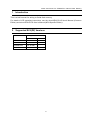
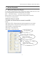
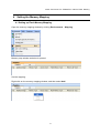
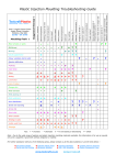
STM32Lxxx Internal Flash Memory
Instructions Manual
Yokogawa Digital Computer Corporation
Notes and Points for STM32Fxxx Internal Flash Memory
(1)
No part of this manual may be reproduced or transmitted in any form or by any means,
electronic or mechanical, without the written permission of Yokogawa Digital Computer
Corporation.
(2)
The contents of this manual are subject to change without prior notice due to
improvement of the functionality.
(3)
If any question about the contents of this manual arises, contact Yokogawa Digital
Computer Corporation.
(4)
Yokogawa Digital Computer Corporation shall not be held responsible for direct or
indirect adverse effects resulting from operation of this system irrespective of the
above item (3).
(5)
Product and company names mentioned in this manual are the trademarks of their
respective owners.
© 2012
Yokogawa Digital Computer Corporation.
Printed in Japan
II
All Rights Reserved.
Notes and Points for STM32Fxxx Internal Flash Memory
Revision History
Edition
Date of issue
Description
1st Edition
Sep. 30, 2013
• Initial publication
III
Notes and Points for STM32Fxxx Internal Flash Memory
Contents
1
Introduction .............................................................................................................5
2
Supported SLX(ZX) Versions .................................................................................5
3
Advance Preparation ..............................................................................................6
3.1
MPU-specific Debug Control Register.............................................................................................. 6
3.2
Changing I/F to connect.................................................................................................................... 7
4
4.1
Setting the Memory Mapping .................................................................................8
Setting up Flash Memory Mapping ................................................................................................... 8
5
Erase the Flash Memory.......................................................................................10
6
Download to Flash Memory .................................................................................10
6.1
Downloadable Area ......................................................................................................................... 10
6.2
Downloading the readout protection (RDP) area ........................................................................... 10
7
Software Break in Flash Memory......................................................................... 11
8
Notes & Points.......................................................................................................12
8.1
Memory write protection.................................................................................................................. 12
IV
Notes and Points for STM32Fxxx Internal Flash Memory
1
Introduction
This is a brief manual for writing to Serial flash memory.
For details of ICE operating instructions, see the microVIEW-PLUS User’s Manual (Common
Edition) and microVIEW-PLUS User’s Manual (MPU-Specific Edition).
2
Supported SLX(ZX) Versions
Device Model
Supported Versions
SLX600
ZX600
STM32L100
2.51 or later
--
STM32L151
2.51 or later
--
STM32L152
2.51 or later
--
STM32L162
2.51 or later
--
5
Notes and Points for STM32Fxxx Internal Flash Memory
3
3.1
Advance Preparation
MPU-specific Debug Control Register
In some cases, Cortex-M series core has a debug control register outside of the core. In this
case, start debugging after setting the debug specific control register.
(MPU → MPU-Specific Setting → Synchronous memory operation)
Without settings, you may not be able to perform debug operation successfully.
The followings are setting examples.
* Modify the settings as required.
* For details, see technical reference manuals for each MPU.
Settings
DBG_IWDG_STOP=1: Debug independent watchdog stopped when core is halted.
DBG_WWDG_STOP=1: Debug Window Watchdog stopped when Core is halted.
DBG_STANDBY=1: Debug Standby mode.
DBG_STOP=1: Debug Stop mode.
DBG_SLEEP=1: Debug Sleep mode.
Select After Reset
Set “0x00000007” for Debug
specific control register
(DBGMCU_CR: 0xe0042004).
Set
“0x00001800”
for
Debug
specific control register
(DBGMCU_APB1: 0xe0042008).
6
Notes and Points for STM32Fxxx Internal Flash Memory
3.2 Changing I/F to connect
In case the debugger operation in SWD is unstable, switch it to JTAG I/F. Set the number of
bypass TAP at pre-stage and the number of IR register bit at pre-stage then.
7
Notes and Points for STM32Fxxx Internal Flash Memory
4
Setting the Memory Mapping
4.1 Setting up Flash Memory Mapping
Open the memory mapping window by clicking Environments – Mapping.
Memory map window as below is opened.
Set the mapping.
Right-click on the memory mapping window, and then select Add.
8
Notes and Points for STM32Fxxx Internal Flash Memory
Configure the setting as the example below.
*1
Select Flash memory
*2
Select 32bit x 1
*1: Set the address in accordance with a mapping block.
*2: Select the flash memory definition file (.frd) in accordance with the mapping block.
The following table describes about the mapping blocks, starting addresses, and frd files.
・Setup example for when using STM32L151CC
Mapping block
*1 Start address
*2 Flash Memory Type
Program memory
0x08000000
STM32L151CC_Program.frd
Data Memory / EEPROM
0x08080000
STM32L151CC_Data.frd
Option byte block
0x1FF80000
STM32L151CC_OptionBytes.frd
9
Notes and Points for STM32Fxxx Internal Flash Memory
5
Erase the Flash Memory
For details, see the microVIEW-PLUS User’s Manual (MPU-Specific Edition).
Details of memory mapping settings are described on this manual. Please refer to the
microVIEW-PLUS User’s Manual (MPU-Specific Edition) for other contents.
6
Download to Flash Memory
For details, see the microVIEW-PLUS User’s Manual (MPU-Specific Edition).
Details of memory mapping settings are described on this manual. Please refer to the
microVIEW-PLUS User’s Manual (MPU-Specific Edition) for other contents.
6.1 Downloadable Area
Flash memory of STM32L1xx series is sectioned as the following table.
You can program the area marked “Yes”.
Block
Item
Start address
Size
Supported
0x08000000
128KB to 384KB
Yes
DATA
0x08080000
4KB to 12KB
Yes
System memory
0x1FF00000
4KB to 8KB
No
Option bytes
0x1FF80000
32B to 64B
Yes
Program memory
Data memory/
EEPROM
Information block
block
Note:
(1) System memory area of information block cannot be overwritten due to the specification of
MPU.
6.2 Downloading the readout protection (RDP) area
Data programming to an area which controls readout protection (RDP) in an option bytes block
of information block is not download data. The data is always being protected at level 0.
Data actually programmed into that area is as follows.
Write address
Setting value
0x1ff80000
0xFF5500AA
Depending on the specification of chip, mass erase may be executed if you download data into
RDP area when readout protection is at level 1(memory read protection enabled) condition. As
a result, program area, data EEPROM area and option byte area are all erased.
10
Notes and Points for STM32Fxxx Internal Flash Memory
7
Software Break in Flash Memory
For details, see the microVIEW-PLUS User’s Manual (MPU-Specific Edition).
Details of memory mapping settings are described on this manual. Please refer to the
microVIEW-PLUS User’s Manual (MPU-Specific Edition) for other contents.
You are not allowed to set up software break for flash memory in the initial state. In case you try
to set up software break for flash memory in the disabled status, it results in “ICE Error No. 8c4:
Set Software Break Verify Error”.
To enable software break setting for flash memory, select the Enable checkbox of S/W Break
in Flash Memory on the Others tab of the MPU-Specific Settings dialog box.
11
Notes and Points for STM32Fxxx Internal Flash Memory
8
Notes & Points
8.1 Memory write protection
Depending on the specification of chip, the system will be reset when releasing the protection.
Therefore, you cannot program the flash (*) while setting the memory write protection which
uses option byte area.
Please release the memory write protection before programming the flash.
*: Programming which is accompanied by downloading, erasing and software break setting of
the on-chip flash memory.
12