1
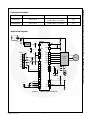
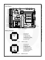
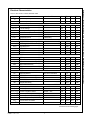
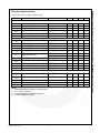
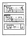
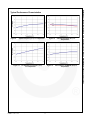
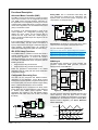
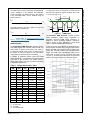
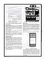
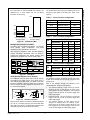
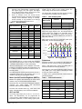
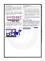
FCM8531 — MCU Embedded and Configurable 3-Phase PMSM / BLDC Motor Controller Features Description Advanced Motor Controller (AMC) Configurable Processing Core - Sensorless Field-Oriented Control (FOC) with Speed Integral Method - Sensorless FOC with Sliding Mode - Hall Interface Space Vector Modulation (SVM) Sine-Wave & Square-Wave Generator Programmable Current Leading Phase Control Programmable Soft-Switching Control (Dead Time) FCM8531RQY Certified by UL for IEC-60730-1 Class B Compliance with recognized marking: The FCM8531 is an application-specific parallel-core processor for motor control that consists of an Advanced Motor Controller (AMC) processor and a ® MCS 51-compatible MCU processor. The AMC is the core processor specifically designed for motor control. It integrates a configurable processing core and peripheral circuits to perform FOC and “Sensorless” motor control. System control, user interface, communication interface, and input/output interface can be programmed through ® the embedded MCS 51 for different motor applications. Embedded MCU ® MCS 51 Compatible 63% of Instructions’ Execution Cycle <3 System Clocks (3T) Memory Size: - 12 KB Flash Program Memory - 256 +1 KB SRAM Data Memory Extended16-Bit Multiplication / Division Unit (MDU) ≤17 General-Purpose Input / Output (GPIO) Pins Full Duplex Serial Interface (UART) 2 I C Interface Serial Peripheral Interface (SPI) Three External Interrupts Three 16-Bit Timers Programmable 15-Bit Watchdog Timer (WDT) Built-in Power-On Reset (POR) Built-in Clock Generator Two-Level Program Memory Lock ADC and DAC 8-Channel, 10-Bit ADC - Auto-Trigger Sample & Hold - Four Trigger Mode Selections - Three Pre-AMP Gain Selections 1-Channel, 8-Bit DAC Protections Three Levels of Over-Current Protection (OCP) Power Management Idle Mode, Stop Mode, Sleep Mode Development Supports In System Programming (ISP) On-Chip Debug Support (OCDS) © 2012 Fairchild Semiconductor Corporation FCM8531 • Rev. 1.0.2 The advantage of FCM8531’s parallel-core processors is that the two processors can work independently and complement each other. The AMC processes the tasks dedicated for motor controls, such as the motor control algorithms, PWM controls, current sensing, real-time over-current protection, and motor angle calculation. The embedded MCU provides motor control commands to the AMC to perform motor control activities through a communication interface. This approach reduces the software burden and simplifies the control system program because complex motor control algorithms are executed in the AMC. Fairchild provides the Motor Control Development System (MCDS) IDE and MCDS Programming Kit for users to develop software, compile programs, and perform online debugging. To meet IEC 60730-1 Class B safety standard for household appliances, FCM8531 has FCM8531RQY version in its family that has been certificated by UL for the compliance. Users can directly utilize the UL certificated AMC to quicken product development cycle for electronic controlled PMSM/BLDC motor. Applications Sensorless IPM / SPM, BLDC / PMSM Motor Fan, Blower, Pump, Compressor, etc. Related Resources AN-8202— FCM8531 User Manual - Hardware Description AN-8203— FCM8531 User Manual - Instruction Set User Guide for FCM8531 Evaluation Board www.fairchildsemi.com FCM8531 — MCU Embedded and Configurable 3-Phase PMSM/BLDC Motor Controller November 2013 Part Number Operating Temperature Range FCM8531QY -40 C to 85 C FCM8531RQY -40 C to 85 C Package Packing Method o o 32-Lead, LQFP, JEDEC MS-026, Variation BBA, 7 mm Square Tray o o 32-Lead, LQFP, JEDEC MS-026, Variation BBA, 7 mm Square Tray Application Diagram FCM8531 5V DC-DC Converter A 23 DVDD VA 15 VSEN 0.1µF D 5V AVSS 17 22 AVDD A 0.1µF 5V ISP Port 24 V25 A P02/U 27 1µF P03/X 28 25 DVSS +5V 3.3 D 33 RST 0.1µF 10K D D 12 RST 1nF 33 Motor P06/W 31 P07/Z 32 10K D 3-Phase Inverter P05/Y 30 33 SCL SDA P04/V 29 26 VPP VPP D 1 P10 D 40K 1% IA 21 2 P11 GND 40K 1% IB 20 3 P12 40K 1% IC 19 4 P13 RS <100p 5 P14 6 P15 A A A 5V A 7 P16 NTC 8 P17 VB 14 RUN/STOP 9 P24 5V VC 13 CW/CCW 10 P25 D FAULT 5V OTP ADC0 18 SPEED 11 P26 A ADC3 16 A Figure 1. © 2012 Fairchild Semiconductor Corporation FCM8531 • Rev. 1.0.2 Typical Application Circuit www.fairchildsemi.com 2 FCM8531 — MCU Embedded and Configurable 3-Phase PMSM/BLDC Motor Controller Ordering Information 27 P03 / X 28 P04 / V 29 P05 / Y 30 P06 / W 31 V25 DVSS 23 24 25 2.5V Power Management Unit GPIO 0 P02 / U DVDD SLEEP VPP RST 26 AVSS AVDD 12 17 D 22 A AVDD IBIAS Protection POR 21 IA 20 IB 19 IC 15 VA 14 VB 13 VC 18 ADC0 16 ADC3 / AOUT Short fSYS Clock Generator OC Fault AMC P07 / Z 32 P10 / RX 1 P11 / TX 2 P12 / SCL 3 P13 / SDA 4 P14 / SPSSN 5 P15 / MOSI 6 ISP OCDS 7 WDT MDU UVWXYZ PWM Engine Monitor Bus 9 P25 / CC1 10 P26 / CC2 11 MSFR Configurable Processing Core UART Port P24 / CC0 SRAM DM (1K) Embedded MCU MCS-51 Core SPI 10-bit ADC TIMER GPIO 2 8 GPIO 1 P17 / SCK I/O Peripheral P16 / MISO Angle Predictor Flash PM (12KB) I2C MUX 8-bit DAC SFR Figure 2. Block Diagram 17 F- Fairchild Logo Z- Plant Code X-1-Digit Year Code Y- 1-Digit Week Code TT: 2-Digit Die Run Code T:Package Type (Q=LQFP) P: Y=Green Package M: Die Run Code 16 F ZXYTT FCM8531 TPM 8 1 9 32 25 24 Marking Information 17 F- Fairchild Logo Z- Plant Code X-1-Digit Year Code Y- 1-Digit Week Code TT: 2-Digit Die Run Code R: UL60730 Certification T:Package Type (Q=LQFP) P: Y=Green Package M: Die Run Code 9 8 1 32 F ZXYTT FCM8531R TPM Figure 4. © 2012 Fairchild Semiconductor Corporation FCM8531 • Rev. 1.0.2 FCM8531 Top Mark 16 25 24 Figure 3. FCM8531R Top Mark www.fairchildsemi.com 3 FCM8531 — MCU Embedded and Configurable 3-Phase PMSM/BLDC Motor Controller Block Diagram V25 DVDD AVDD IA IB IC ADC0 AVSS 24 23 22 21 20 19 18 17 25 16 26 15 27 14 28 13 29 12 30 11 31 10 9 32 1 2 3 4 5 6 7 8 DVSS VPP P02 / U P03 / X P04 / V P05 / Y P06 / W P07 / Z P10 / RX / SCL / SPSSN P11 / TX / SDA / MOSI P12 / SCL / RX / MISO / ISP_SCL P13 / SDA / TX / SCK / ISP_SDA P14 / SPSSN / TDO / RX / SCL P15 / MOSI / TDI / TX / SDA P16 / MISO / TMS / SCL / RX P17 / SCK / TCK / SDA / TX FCM8531 ADC3 / AOUT VA VB VC RST P26 / CC2 / T2 / T0 P25 / CC1 / T1 / T2EX P24 / CC0 / T0 / T2 Figure 5. Pin Configuration Pin Definitions Pin # 1 2 3 4 5 Name Type Description P10 I/O RX I SCL I/O Serial Clock (I C) SPSSN I/O SPI Slave Select (SPI) P11 I/O Bit 1 of Port 1. General-purpose input/output pin with internal pull-up resistor. TX O Serial Data Transmit (UART) SDA I/O Serial Data (I C) MOSI I/O Master Data Output and Slave Data Input (SPI) P12 I/O Bit 2 of Port 1. General-purpose input/output pin with internal pull-up resistor. SCL I/O Serial Clock (I C) RX I MISO I/O Master Data Input and Slave Data Output (SPI) ISP_SCL I ISP Serial Clock. Serial clock input in ISP Mode. P13 I/O Bit 3 of Port 1. General-purpose input/output pin with internal pull-up resistor. SDA I/O Serial Data (I C) TX O Serial Data Transmit (UART) Bit 0 of Port 1. General-purpose input/output pin with internal pull-up resistor. Data Receive (UART) 2 2 2 Data Receive (UART) 2 SCK I/O Serial Clock (SPI) ISP_SDA I/O ISP Serial Data. Serial data input/output pin in ISP Mode. P14 I/O Bit 4 of Port 1. General-purpose input/output pin with internal pull-up resistor. SPSSN I/O SPI Slave Select (SPI) RX I Data Receive (UART) SCL I/O Serial Clock (I C) TDO O Test Data Output. Test data output in OCDS Mode. 2 Continued on the following page… © 2012 Fairchild Semiconductor Corporation FCM8531 • Rev. 1.0.2 www.fairchildsemi.com 4 FCM8531 — MCU Embedded and Configurable 3-Phase PMSM/BLDC Motor Controller Pin Configuration Pin # 6 7 8 9 10 Name Type Description P15 I/O Bit 5 of Port 1. General-purpose input/output pin with internal pull-up resistor. MOSI I/O Master Data Output and Slave Data Input (SPI) TX O Serial Data Transmit (UART) SDA I/O Serial Data (I C) 2 Test Data Input. Test data input in OCDS Mode. TDI I P16 I/O Bit 6 of Port 1. General-purpose input/output pin with internal pull-up resistor. MISO I/O Master Data Input and Slave Data Output (SPI) SCL I/O Serial Clock (I C) RX I Data Receive (UART) TMS I Test Mode Select. Test mode select in OCDS Mode. P17 I/O Bit 7 of Port 1. General-purpose input/output pin with internal pull-up resistor. SCK I/O Serial Clock (SPI) SDA I/O Serial Data (I C) TX O Serial Data Transmit (UART) TCK I Test Clock. Test clock input in OCDS Mode. P24 I/O Bit 4 of Port 2. General-purpose input/output pin with internal pull-up resistor. CC0 I/O TIMER2 Compare/Capture Channel 0 T0 I TIMER0 External Input TIMER2 External Input 2 2 T2 I P25 I/O Bit 5 of Port 2. General-purpose input/output pin with internal pull-up resistor. CC1 I/O TIMER2 Compare/Capture Channel 1 T1 I TIMER1 External Input T2EX I TIMER2 External Trigger P26 I/O Bit 6 of Port 2. General-purpose input/output pin with internal pull-up resistor. CC2 I/O TIMER2 Compare/Capture Channel 2 T2 I TIMER2 External Input T0 I TIMER0 External Input 12 RST I System Reset. Hardware reset input, active HIGH. 13 VC AI Analog Input. 10-bit ADC input (middle sampling rate). The ADC result stores in VCL and VCH registers (2Ch, 2Dh) of MSFR. 14 VB AI Analog Input. 10-bit ADC input (middle sampling rate). The ADC result stores in VBL and VBH registers (2Ah, 2Bh) of MSFR. 15 VA AI Analog Input. 10-bit ADC input (middle sampling rate). The ADC result stores in VAL and VAH registers (28h, 29h) of MSFR. ADC3 AI Analog Input. 10-bit ADC input (low sampling rate).The ADC result stores in ADC3L and ADC3H registers (36h, 37h) of MSFR. AOUT AO Analog Output. 8-bit DAC output set by DAC3 register (47h) of MSFR. 17 AVSS P Analog Ground 18 ADC0 AI Analog Input. 10-bit ADC input (low sampling rate). The ADC result stores in ADC0L and ADC0H registers (30h, 31h) of MSFR. 19 IC AI Phase C Current Input. 10-bit ADC input (high sampling rate). The ADC result stores in ICL and ICH registers (24h, 25h) of MSFR. 11 16 Continued on the following page… © 2012 Fairchild Semiconductor Corporation FCM8531 • Rev. 1.0.2 www.fairchildsemi.com 5 FCM8531 — MCU Embedded and Configurable 3-Phase PMSM/BLDC Motor Controller Pin Definitions (Continued) Pin # Name Type 20 IB AI Phase B Current Input. 10-bit ADC input (high sampling rate). The ADC result stores in IBL and IBH registers (22h, 23h) of MSFR. 21 IA AI Phase A Current Input. 10-bit ADC input (High sampling rate). The ADC result stores in IAL and IAH registers (20h, 21h) of MSFR. 22 AVDD P 5.0 V Analog Voltage Input. A 0.1 µF (minimum) capacitor should be connected between this pin and AVSS. 23 DVDD P 5.0 V Digital Voltage Input. A 0.1 µF (minimum) capacitor should be connected between this pin and DVSS. 24 V25 O 2.5 V Voltage Regulator Output. A 0.1 µF (minimum) capacitor should be connected between this pin and DVSS. 25 DVSS P Digital Ground 26 VPP P Programming Supply Voltage. VPP = 12 V for flash memory programming. U O PWM Output. High-side gate control signal of phase A. P02 I/O Bit 2 of Port 0. General-purpose input/output pin with internal pull-down resistor. X O PWM Output. Low-side gate control signal of phase A. P03 I/O Bit 3 of Port 0. General-purpose input/output pin with internal pull-down resistor. V O PWM Output. High-side gate control signal of phase B. P04 I/O Bit 4 of Port 0. General-purpose input/output pin with internal pull-down resistor. Y O PWM Output. Low-side gate control signal of phase B. P05 I/O Bit 5 of Port 0. General-purpose input/output pin with internal pull-down resistor. 27 28 29 30 31 32 Description W O PWM Output. High-side gate control signal of phase C. P06 I/O Bit 6 of Port 0. General-purpose input/output pin with internal pull-down resistor. Z O PWM Output. Low-side gate control signal of phase C. P07 I/O Bit 7 of Port 0. General-purpose input/output pin with internal pull-down resistor. Notes: 1. Type P: power pin. 2. Type I: digital input pin. 3. Type O: digital output pin. 4. Type I/O: bidirectional input/output pin. 5. Type AI: analog input pin. 6. Type AO: analog output pin. © 2012 Fairchild Semiconductor Corporation FCM8531 • Rev. 1.0.2 www.fairchildsemi.com 6 FCM8531 — MCU Embedded and Configurable 3-Phase PMSM/BLDC Motor Controller Pin Definitions (Continued) Stresses exceeding the absolute maximum ratings may damage the device. The device may not function or be operable above the recommended operating conditions and stressing the parts to these levels is not recommended. In addition, extended exposure to stresses above the recommended operating conditions may affect device reliability. The absolute maximum ratings are stress ratings only. Symbol Parameter Min. Max. Unit VPP Programming Supply Voltage -0.7 13 V VDD Supply Voltage -0.7 7 V VVIH Voltage of I/O Pin and RST Pin with Respect to GND -0.2 VDD+0.2 V VAN Analog Input Voltage -0.2 VDD+0.2 V JA Thermal Resistance (Junction-to-Air) 80 C/W TA Operating Ambient Temperature Range -40 85 C TSTG Storage Temperature Range -65 150 C ESD Electrostatic Discharge Capability Human Body Model, JESD22-A114 3,000 Charged Device Model, JESD22-C101 1,250 V Recommended Operating Conditions The Recommended Operating Conditions table defines the conditions for actual device operation. Recommended operating conditions are specified to ensure optimal performance to the datasheet specifications. Fairchild does not recommend exceeding them or designing to Absolute Maximum Ratings. Symbol Parameter Min. Typ. Max. Unit VDD Supply Voltage 4.5 5.0 5.5 V VPP Programming Supply Voltage 11.8 12.0 12.2 V © 2012 Fairchild Semiconductor Corporation FCM8531 • Rev. 1.0.2 www.fairchildsemi.com 7 FCM8531 — MCU Embedded and Configurable 3-Phase PMSM/BLDC Motor Controller Absolute Maximum Ratings VDD=5 V, and TA=25C unless otherwise noted. Symbol Parameter fSYS System Frequency fSYS System Frequency Conditions At -40C Min. Typ. Max. Unit 29.4 30.0 30.6 MHz 31.5 MHz 4.5 V 28.5 Power Management VDD_ON Turn-On Voltage VDD_OFF Turn-Off Voltage VOUT IDD_OPER (7) IDD_SLEEP (7) tSLEEP 3.2 V25 Output Voltage Range Load Current < 10 mA VDD Current at Operation Mode 20 kHz PWM Output VDD Current at Sleep Mode Wake-up Period = 37 ms Sleep Mode Period Initial Setting V 2.35 2.50 2.65 V 20 29 35 mA 500 40 µA ms (7) Flash Memory VPP Program/Erase Supply Voltage IVPP Mass Program Current tWRITE Page Write Time tERASE Erase Time Endurance 11.8 12.0 12.2 V 8 mA 1.55 500 Erase + Write Data Retention ms 600 ms 1000 cycle 100 year (7) 10-Bit ADC 3 MΩ VI_MIN RI Input Impedance Minimum Conversion Voltage Code 000h 0 V VI_MAX Maximum Conversion Voltage Code 3FFh 4 V DNL Differential Nonlinearity ±2.0 LSB INL Integral Nonlinearity ±2.0 LSB Offset Error ±3.0 LSB ErrADC (7) 8-Bit DAC Output Impedance W/I, W/O Current Bias 10 kΩ VO_MIN RO Minimum Conversion Voltage Code 00h 50 mV VO_MAX Maximum Conversion Voltage Code FFh 4 V DNL Differential Nonlinearity ±1.0 LSB INL Integral Nonlinearity ±2.0 LSB Current Limit VOCL_OFFSET OCL Comparator Offset OCL = 10h -50 50 mV VOCH_OFFSET OCH Comparator Offset OCH = C0h -50 50 mV SHORT = C0h -50 50 mV VSHORT_OFFSET SHORT Comparator Offset VOCL_RNG (7) OCL Comparator Operation Range 0 3.5 V (7) OCH Comparator Operation Range 1 4 V SHORT Comparator Operation Range 1 4 V 52.5 µA 51 µA VOCH_RNG VSHORT_RNG (7) IBIAS Current Source of IA/IB/IC (7) IBIAS Current Source of IA/IB/IC 47.5 At -40C 46 50.0 Continued on the following page… © 2012 Fairchild Semiconductor Corporation FCM8531 • Rev. 1.0.2 www.fairchildsemi.com 8 FCM8531 — MCU Embedded and Configurable 3-Phase PMSM/BLDC Motor Controller Electrical Characteristics VDD=5 V, and TA=25C unless otherwise noted. Symbol Parameter Conditions Min. Typ. Max. Unit GPIO VIH Input High Voltage VIL Input Low Voltage (7) RUP (7) RDOWN SPI 3.3 V 1.8 V P1, P2 Pull-Up Resistor 40 kΩ P0, RST Pull-Down Resistor 45 kΩ IOL Low Level Output Current VOL = 0.4 V 2.3 mA IOH High Level Output Current VOH = 0.8 x VDD 2.5 mA tR(SCK) SPI Clock Rising Time Master Mode, CL = 20 pF 60 ns tF(SCK) SPI Clock Falling Time Master Mode, CL = 20 pF 60 ns tSCK SPI Clock Cycle Time tSYS x 8 ns tENS SSN Setup Time tSYS x 3 ns tHS SSN Hold Time tSYS x 3 ns tDS Data Input Setup Time tDH(MO) (7,9) Slave Mode Master Mode tSYS ns Slave Mode tSYS ns Data Output Hold Time Master Mode tSYS ns tDH(SO) Data Output Hold Time Slave Mode tSYS ns tDH(MI) Data Input Hold Time Master Mode tSYS ns tDH(SI) Data Input Hold Time Slave Mode tSYS ns Data Output Disable Time Slave Mode tDIS(SO) 2 I C Interface tSCL 2 I C Clock Cycle Time tSYS x 120 ns tSCL / 2 ns 2 tSCL / 2 ns 2 tSYS ns 2 tSYS ns I C Start Bit Setup Time tSTOP I C Stop Bit Setup Time tHOLD ns 2 tSTART tSETUP tSYS x 3 (7,10) I C Data Setup Time I C Data Hold Time Notes: 7. These parameters are not tested in manufacturing. 8. tSYS = 1 / fSYS = 33.33 ns. 9. SPI timing diagrams as Figure 6 and Figure 7. 2 10. I C timing diagram as Figure 8. © 2012 Fairchild Semiconductor Corporation FCM8531 • Rev. 1.0.2 www.fairchildsemi.com 9 FCM8531 — MCU Embedded and Configurable 3-Phase PMSM/BLDC Motor Controller Electrical Characteristics Slave Mode, CPHA=1, CPOL=0 SSN tENS tSCK tHS SCK tDH(SO) tDIS(SO) MSB OUT MISO tDS MOSI BIT6 OUT BIT1 OUT BIT6 IN BIT1 IN LSB OUT tDH(SI) MSB IN Figure 6. LSB IN SPI Timing Diagram– Slave Mode Master Mode, CPHA=1, CPOL=0 SSN tENS tSCK tR(SCK) tF(SCK) SCK tDS tDH(MI) MSB IN MISO BIT6 IN BIT1 IN LSB IN tDH(MO) MOSI MSB OUT BIT6 OUT LSB OUT SPI Timing Diagram – Master Mode Figure 7. tSCL BIT1 OUT tHOLD SCL SDA (IN) tSTART tSETUP Figure 8. © 2012 Fairchild Semiconductor Corporation FCM8531 • Rev. 1.0.2 tSTOP 2 I C interface Timing Diagram www.fairchildsemi.com 10 FCM8531 — MCU Embedded and Configurable 3-Phase PMSM/BLDC Motor Controller Timing Diagrams 0mA 10mA Figure 9. System Frequency (fSYS) vs. Temperature Figure 11. VDD Operation Current (IDD_OPPER) vs. Temperature © 2012 Fairchild Semiconductor Corporation FCM8531 • Rev. 1.0.2 Figure 10. Figure 12. V25 Output Voltage (VOUT) vs. Temperature Current Source of IA/IB/IC (IBIAS) vs. Temperature www.fairchildsemi.com 11 FCM8531 — MCU Embedded and Configurable 3-Phase PMSM/BLDC Motor Controller Typical Performance Characteristics Sliding Mode: this is a Sensorless FOC library with more parameters to adjust and set. Applications with dynamic loads; such as water pumps, oil pumps, and compressors; can adopt this library. Advanced Motor Controller (AMC) The AMC is used for motor driving. It consists of several motor control modules; such as configurable processing core, PWM engine, and angle predictor. Depending on the application, the configurable processing core can be configured with suitable AMC library to perform different motor control algorithms, such as Field-Oriented Control (FOC) or sensorless control. SAW Generator Iq_cmd + DUTY PI DUTYa AS Iq Vq + AS PI q’ Inverse Park - For example, if the Sensorless library is used as the control algorithm, the configurable processing core obtains the motor current via the internal ADC to estimate the rotor angle. After that, a PWM engine is used to provide the PWM output drive signal to set the correct rotor angle. SVM Table PWM Engine DUTYb DUTYc Id U V W X Y Z Vα,Vβ q qEstimater Iα,Iβ Park Figure 14. Clarke Ia Ib Ic Current Feedback IA IB Sliding Mode Block Diagram If the configurable processing core is configured with the Hall Interface library, the rotor position information is input by GPIO and the rotor angle is estimated using the angle predictor. The PWM engine can provide the appropriate PWM output drive signals for motor driving. Hall Interface: this library is used in Hall sensor motor control systems with square / sinusoidal wave drive. IEC 60730 Safety Functions AMC Library User Guide - Speed Integral for FCM8531 The FCM8531RQY is certified to meet the IEC 60730-1 Class-B standards; which cover mechanical, electrical, and electronic appliances. To achieve IEC 60730-1 Class-B requirements, the safety functions are included in the AMC of FCM8531RQY and in compliance with the following structures: AMC Library User Guide - Sliding Mode for FCM8531 For more information, please see: AMC Library User Guide - Hall Interface for FCM8531 PWM Engine The PWM engine includes four circuit modules: saw generator, square-wave PWM generator, sine-wave PWM generator, and PWM MUX. Single channel using functional test. Single channel using periodic functional test. Follow the procedures recommended in the related application notes to comply with IEC 60730 certification in application designs. PWM Engine Cycle by Cycle Off Protection Square-Wave PWM Generator Configurable Processing Core The AMC can be configured with different libraries, depending on the application, via the Motor Control Development System (MCDS) Integrated Development Environment (IDE). For example: Speed Integral, Sliding Mode, or Hall Interface libraries can be activated. Figure 15. DUTYa Vq + 0 PI q’ AS SVM Table Inverse Park - DUTYb PWM Engine DUTYc Id U V W X Y Z UP-DOWN Vα,Vβ q Park Figure 13. qEstimater Iα,Iβ Clarke Ia Ib Ic PWM Engine Block Diagram The saw generator determines the PWM waveform and carrier frequency. There are three modes of carrier waveforms; UP, DOWN, and UP-DOWN; set using the SAWMOD bit in the SAWCNTL register in MSFR (Motor Special Function Registers) (see Error! Reference source not found.). SAW Generator DUTY W Z Sine-Wave PWM Generator Angle Angle Predictor Speed Integral: this is a sensorless FOC library where D-axis phase error is compensated by a large integrator to achieve more stable speed response. Fewer parameters are required to set with Speed Integral. Applications with static load, such as fans, can adopt this library. PWM MUX SAW Generator MSFR U X V Y UP Current Feedback IA DOWN IB Speed Integral Block Diagram Figure 16. © 2012 Fairchild Semiconductor Corporation FCM8531 • Rev. 1.0.2 SAW Output Mode www.fairchildsemi.com 12 FCM8531 — MCU Embedded and Configurable 3-Phase PMSM/BLDC Motor Controller Functional Description In square-wave mode, the PWM duty is determined by the DUTYA and DUTYAL registers in MSFR, with a total of 11 bits (see Figure 17). PWM Cycle SAW SAW Count DUTY (1) PWM The PWM frequency formula for SAW in the UP and DOWN modes is calculated by: dead-time PWMb Figure 17. (2) The Sine-Wave PWM Generator includes a Space Vector Modulation (SVM) circuit responsible for generating sine-wave PWM output waveforms. In addition to built-in sinusoidal waveform modulation, which is popular in many applications, a table allows users to customize PWM output waveforms. Please refer to AN-8202—FCM8531 User Manual - Hardware Description for details. SAW Generator In sine-wave mode, the PWM duty is determined by the DUTYA register in MSFR. When using the Hall interface library, the PWM engine starts the motor in square-wave mode. After the angle predictor can accurately predict angles, the PWM engine automatically shifts to sinewave mode. As shown in Figure 18 (CW=0) and Figure 19 (CW=1), corresponding PWM signals are generated based on the angle estimated from Hall input signals. The Square-Wave PWM Generator generates squarewave PWM signals with a default pattern based on a built-in table of default square-waves (see Table 1). Corresponding PWM output signals are determined by the pattern of Hall input signals or the Hall register, while direction is determined by the CW setting. In addition to generating default square-wave PWM output waveforms, a customizable user-defined squarewave table is also provided. This enables users to define special square-wave output waveforms according to application requirements. Table 1. PWM Output Default Square-Wave Table CW Hall Hall U-V-W X-Y-Z X 000 0 000 000 X 111 7 000 000 1 001 1 P00 Pb 1 0 1 011 3 00P 0 1 Pb 1 010 2 00P 1 0 Pb 1 110 6 0P0 1 Pb 0 1 100 4 0P0 0 Pb 1 1 101 5 P00 Pb 0 1 0 101 5 00P 1 0 Pb 0 100 4 00P 0 1 Pb 0 110 6 P00 Pb 1 0 0 010 2 P00 Pb 0 1 0 011 3 0P0 0 Pb 1 0 001 1 0P0 1 Pb 0 Figure 18. Default Sine-Wave PWM Output (CW=0) Notes: 11. X: don’t care. 12. P: PWM. 13. Pb: PWM inverse. © 2012 Fairchild Semiconductor Corporation FCM8531 • Rev. 1.0.2 www.fairchildsemi.com 13 FCM8531 — MCU Embedded and Configurable 3-Phase PMSM/BLDC Motor Controller The PWM carrier frequency is decided by the PRESCAL and the POSSCAL in the SPRDH/L and SAWCNTL registers in MSFR. The PWM frequency, when SAW is in the UP-DOWN Mode, can be obtained using the following formula: External Memory 1024B Embedded MCU OCDS Interface OCDS Stack Pointer Memory Interface Data Bus B Reg. Clock Reset 16 Program Address Reg. 8 ACC Control Logic TMP2 Inst. Reg. Buffer SRAM 256B TMP1 DPTR PC Incrementer ALU SRAM Address Reg. PSW PC ISR Interface Power Control Reg. IDLE STOP SLEEP SFR MDU WDT EXTINT TIMER0 I2C UART SPI TIMER1 PORT0 PORT1 PORT2 TIMER2 GPIO Figure 20. Embedded MCU Block Diagram Memory Map Figure 19. Default Sine-Wave PWM Output (CW=1) The 12KB flash program memory is divided into two parts. In the first section of the memory area, addresses 0000h~2EFFh, are used to store programs. Addresses higher than 2EFFh are in the special area, including two groups of user-definable wave tables and one lock byte. When 0 is written into the highest bit of the lock byte, the OCDS function is disabled. When 0 is written into any other bit, the flash memory is encrypted to secure the program code. Angle Predictor When using Hall sensors for sine-wave control, the Hall signals are used to accurately predict the rotor position of the motor. This information is provided to the SVM circuit to calculate the space vector. Two circuits are included in the angle predictor: Hall signal filter and leading-angle shifter. The Hall signal filter is responsible for Hall signal debounce, blanking, regulation, and inversion. Flash memory must first be erased and then re-written. 2FFFh 2FFEh The rotor position can be adjusted using the leadingangle shifter. This can compensate for the current lag caused by motor winding inductance and further improve the motor efficiency. 2FC0h Embedded MCU 2F00h System flow control, user interface, input/output, and communication interface can be programmed and set in the embedded MCU. The instruction set is fully ® compatible with MCS 51; therefore, a standard 805x assembler and compiler can be used for development. Lock Byte User Defined Square-Wave Table User Defined Sine-Wave Table Program Code Since FCM8531 uses advanced instruction architecture that only needs one system clock per instruction set, its computation speed is greatly improved compared with the conventional 8051 MCU, which needs 12 system clocks per instruction set. 0003h 0000h In addition to the normal 8051 MCU functions; such as GPIO, TIMER0/1/2, ISR, and UART; other 2 communication interfaces; such as SPI, I C, and Watchdog Timer (WDT) functions; are also integrated into the embedded MCU. © 2012 Fairchild Semiconductor Corporation FCM8531 • Rev. 1.0.2 MSFR Interrupt Vector Reset Vector Program Memory 12 KBytes Flash Figure 21. Program Memory Map Four groups of register banks are provided in the 256byte internal SRAM data memory. The first 128 bytes (00h~7Fh) of the internal data memory can be read by immediate addressing or indirect addressing. The latter 128 bytes (80h~FFh) in the memory are overlapped with SFR. Accessing data in SRAM must use indirect addressing, while SFR uses immediate addressing to read and write. www.fairchildsemi.com 14 FCM8531 — MCU Embedded and Configurable 3-Phase PMSM/BLDC Motor Controller Flash Memory 12KB The multi-function pins P1[7:0] and P2[6:4] can be set through IO_CFG (F9h) of the SFR (see Table 3 and Table 4). 3FFh Table 2. Port 0 Function Configuration P0_CFG 0 (Default) 1 Bit 7 PWM Z Channel P07 Bit 6 PWM W Channel P06 Bit 5 PWM Y Channel P05 80h Bit 4 PWM V Channel P04 30h 20h 00h Bit 3 PWM X Channel P03 Bit 2 PWM U Channel P02 FFh SFR Bit Addr. Space Reg. Bank x4 000h Internal Data Memory 256 Bytes SRAM Figure 22. Table 3. External Data Memory 1024 Bytes SRAM Pin Data Memory Map 01 10 11 RX SCL SPSSN SPSSN P11 TX SDA MOSI MOSI P12 SCL RX MISO MISO SDA TX SCK SCK SPSSN SPSSN RX SCL MOSI MISO TX SDA P16 MISO MISO SCL RX P17 SCK SCK SDA TX P10 The MDU, used for parallel calculations, can process 32-bit division, 16-bit multiplication, and 32-bit displacement and normalization calculations. After setting the calculation model, the MDU begins to execute calculation. Meanwhile, MCU are freed to continue the subsequent flow without pausing. After calculation is completed, the result is stored in SFR. P13 P14 P15 Mode 3 17 cycles 32 bits 11 cycles 16 bits Result Result 16 bits 16 bits Mode 2 Table 4. Mode 4 9 cycles Pin 3~19 cycles 16 bits Result 32 bits 16 bits Figure 23. IO_CFG[1:0] 00 (Default) Multiplication-Division Unit (MDU) Mode 1 Port 1 Function Configuration Shift /Normalizing Result P24 P25 P26 MDU Mode Port 2 Function Configuration 00 (Default) CC0 CC1 CC2 IO_CFG[3:2] 01 10 CC0 CC1 CC2 T0 T1 T2 11 T2 T2EX T0 GPIO (General-Purpose Input / Output) Interrupt The FCM8531 has three GPIO ports: P0[7:2], P1[7:0], and P2[6:4]. The output can be set to direct drive or open drain through DIR0, DIR1, and DIR2 of the SFR. Inside the FCM8531, P0[7:2] is pulled down to GND by internal resistors and other digital IOs are pulled up to 5 V with internal resistors. The FCM8531 provides 16 interrupt sources (see Table 5) that can be divided into five priority groups and four priority levels. 5V 5V Set DIR Port out Most of the interrupt settings are identical to the standard MCS51, except for the following: P0[2:7] P1[0:7] P2[4:6] Port out Set DIR Port input Figure 24. Port input GPIO Driver & Buffer P0[7:2] can be defined as a GPIO or PWM output signal (U, V, W, X, Y, and Z) by using P0_CFG of the SFR. After reset, P0[7:2] is pre-set to a PWM output signal and the other DIO pins are pre-set as GPIO (see Table 2). © 2012 Fairchild Semiconductor Corporation FCM8531 • Rev. 1.0.2 The external interrupt 0 input source pin can be assigned to P24 or P26 through IO_CFG of the SFR (Special Function Registers). The interrupt trigger mode can be set to low-level trigger and falling-edge trigger. External interrupt 1 is input via P25. The interrupt trigger mode can be set to low-level trigger and falling-edge trigger. The external interrupt 12 input signal can be assigned to P1[6:0]. When an interrupt occurs, INT12_STA can be used to inspect which pin has been triggered. The interrupt trigger mode can be set to low-level trigger and falling-edge trigger. www.fairchildsemi.com 15 FCM8531 — MCU Embedded and Configurable 3-Phase PMSM/BLDC Motor Controller The 1024 bytes of external SRAM data memory are addressed by a 16-bit DPTR and use an MOVX instruction for accessing. Table 5. depending on the application. The ADC3/AOUT pin location can be used as 0~4 V analog output. The output voltage is set via the DAC in the MSFR. The internal ADC is divided into three groups according to the speed of the sampling rate (see Table 6). Table 6. Sampling Rate Speed Interrupt Vector Interrupt Source Interrupt Symbol Vector External Interrupt 0 Timer 0 Overflow External Interrupt 1 Timer 1 Overflow Serial Timer2 2 IC SPI COM0 COM1 COM2 FAULT ADC Ready Trigger 0003h 000Bh 0013h 001Bh 0023h 002Bh 0043h 004Bh 0053h 005Bh 0063h 008Bh 0093h EX0 ET0 EX1 ET1 ES0 ET2 EX7 EX2 EX3 EX4 EX5 EX8 EX9 Hall Edge 009Bh EX10 AMC 00A3h EX11 External Interrupt 12 00ABh EX12 ADC Sampling Rate Trigger Fall, Low Channel Convert Period High IA, IB, IC 1 ADC Trigger Mid VA, VB, VC 4 ADC Trigger Low ADC0, ADC3 16 ADC Trigger Pins IA, IB, and IC are preset as current-sensing input. When ADC trigger signals occur, the sample-and-hold circuits retrieve the voltage to be converted. Then it goes through a pre-amplifier to a 10-bit A-D converter. After conversion, it is stored in MSFR and generates an ADC-ready interrupt. Fall, Low ADC trigger mode has four sub-modes: SAW peak, SAW valley, Timer0, and manual trigger. Rise, Fall Rise Rise SAW TMR0 SAW Peak Rise, Fall, Rise & Fall Rise Rise, Fall, Rise & Fall SAW Valley TMR0 Figure 25. Watchdog Timer (WDT) ADC Trigger Mode Protections The watchdog timer is a 15-bit counter that increases every 384 or 6144 system cycles. If there are software or hardware abnormalities, it resets automatically. Protection functions are provided for Hall signal error protection and over-current (cycle-by-cycle) protection. When a Hall signal error occurs, the PWM pulse is turned off until the error status is released. When the watchdog timer is set in WDTREL of the SFR, it begins to count when the SWDT bit of SFR IEN1 is set to 1. When it counts to 7FFCh and a timeout occurs, it internally resets. Cycle-by-cycle over-current protection (OCP) monitors every PWM cycle. If over-current is detected, the PWM is turned off until the next cycle. The watchdog timer must be refreshed before timeout. If unexpected errors occur, the watchdog timer is not refreshed. After timeout, the program restarts. In addition to the cycle-by-cycle OCP, other protections generate interrupts. Motor Special Function Registers (MSFRs) Table 7. MSFRs are registers used exclusively for motor control modules. They are accessed through MCU SFRs. Type Condition Action Parameters such as motor control, Hall signal configure, waveform type, PWM engine, and over-current protection level can be set in MSFRs. Hall Slow Hall Period Overflow Interrupt 8 Short A IA > ISHORT Interrupt 8 Short B IB > ISHORT Interrupt 8 The ADC and controller status (e.g., Fault status, Hall status, and PWM status) can be obtained via MSFRs. Short C IC > ISHORT Interrupt 8 ADC and DAC Hall Error Hall Sensor = 111 or 000 Interrupt 8 PWM Off The analog signal input pins (IA, IB, IC, VA, VB, VC, ADC0, and ADC3/AOUT) can be programmed for current sensing, voltage feedback, speed control, overtemperature protection, or other analog signal inputs; OC High IA / IB / IC > IOCH PWM Off OC Low IA / IB / IC < IOCL PWM off © 2012 Fairchild Semiconductor Corporation FCM8531 • Rev. 1.0.2 Fault and Protection www.fairchildsemi.com 16 FCM8531 — MCU Embedded and Configurable 3-Phase PMSM/BLDC Motor Controller The other interrupt sources include: VDD low-voltage warnings, ADC transformation completion trigger, Hall signal trigger, slow Hall signal, Hall signal error, and short-circuit sensing. These can be used for developing the motor control system. When an interrupt occurs, the interrupt service executes interrupt service programs at the specified interrupt vector addresses. During an interrupt, another interrupt is only permitted if an interrupt source with a higher priority level occurs. Power Management There are three methods of current protection: negative over current, positive over current, and short-circuit sensing. The protection points can be set via the OCL, OCH, and SHORT of MSFR. After a protection is triggered, PWM is immediately turned off until the next cycle (cycle-by-cycle). If VDD is > VDDON, the reset status takes about 2 ms to be released. FCM8531 provides three kinds of power-saving modes: When the input voltage is higher than the SHORT voltage, an EX8 interrupt is generated. Corresponding measures can be executed to protect system based on requirements of application systems. SHORT OCH Phase Current VBIAS OCL In IDLE mode; execution of MCU programs pauses, but the peripheral I/O circuits continue to work (e.g. PWM, external interrupt, timing, serial output, etc.). In STOP mode; execution of programs, digital I/O interfaces, and all digital circuits pause. This mode continues until the occurrence of an EX0/EX1 external interrupt or a system reset. In SLEEP mode, the MCU and AMC are both turned off. At this moment, the alarm timer begins to count. After a timeout, the MCU and AMC are turned on again. Development Supports PWM Cycle by cycle limit Figure 26. Fairchild provides the Motor Control Development System (MCDS) Integrated Development Environment ® (IDE). On Microsoft Windows platforms, functions such as project building, program code generation, compilation, In-System Programming (ISP), and OnChip Debug Support (OCDS) are supported. This facilitates software development and debugging. Fault Interrupt Current Protection (Square-Wave) Each current-sensing pin (IA, IB, and IC) has an output of 50 µA of bias current. The recommended setting for the bias voltage is 2.0 V (RBIAS= 40 kΩ). VBIAS = IBIAS x RBIAS For detailed information please see: User Guide for MCDS IDE of FCM8531. (3) VP FCM8531 INVERTER IBIAS M 50uA SHORT Protect IA + - SHORT IB IC + Cycle-by -Cycle Protect RBIAS - OCH + OCL RS - Figure 27. Current Feedback Circuit © 2012 Fairchild Semiconductor Corporation FCM8531 • Rev. 1.0.2 www.fairchildsemi.com 17 FCM8531 — MCU Embedded and Configurable 3-Phase PMSM/BLDC Motor Controller Current Protections SFRs (Special Function Registers) Map Hex X000 X001 X010 X011 X100 X101 X110 F8 P0_CFG IO_CFG INT12_CFG INT12_STA DIR0 DIR1 DIR2 F0 B E8 E0 ACC D8 ADCON D0 PSW C8 T2CON C0 IRCON B8 MD0 MD1 MD2 MD3 SPSTA SPCON SPDAT SPSSN I2CDAT I2CADR I2CCON MD4 MD5 X111 Hex FF SRST F7 ARCON EF E7 DF I2CSTA D7 CRCL CRCH TL2 TH2 CF CCEN CCL1 CCH1 CCL2 CCH2 C7 IEN1 IP1 SRELH B0 MTX0 MTX1 MTX2 A8 IEN0 IP0 SRELL A0 P2 98 SCON 90 P1 88 TCON 80 P0 Table 9. Hex MTX3 MRX0 MRX1 MRX2 IRCON2 BF MRX3 B7 AF A7 SBUF 9F IEN2 MSFRADR MSFRDAT 97 DPS DPC TMOD TL0 TL1 TH0 TH1 CKCON SP DPL DPH DPL1 DPH1 WDTREL PCON 87 X110 X111 Hex 8F MSFRs (Motor Special Function Registers) Map X000 X001 X010 X011 X100 X101 78 7F 70 78 68 6F 60 67 58 5F 50 57 48 4F 40 MBUSCTL PT01 PT23 SLEEP OCH OCL SHORT DACO 47 38 Reserved Reserved Reserved Reserved Reserved Reserved ANGLE MSTAT 3F 30 ADC0L ADC0H ADC3L ADC3H 37 28 VAL VAH VBL VBH VCL VCH ADCINX BAK 2F 20 IAL IAH IBL IBH ICL ICH OCCNTL OCSTA 27 18 HALMXU HALFLT HALSTA HALINT HPERL HPERM HPERH ADCCFG 1F 10 Reserved Reserved Reserved Reserved Reserved Reserved Reserved 17 08 PWMCFG SAWCNTL SPRDL SPRDH SDLYBL SDLYBH SDLYCL SDLYCH 0F 00 MCNTL ANGCTL AS ANGDET DUTYAL DUTYA DUTYB DUTYC 07 © 2012 Fairchild Semiconductor Corporation FCM8531 • Rev. 1.0.2 www.fairchildsemi.com 18 FCM8531 — MCU Embedded and Configurable 3-Phase PMSM/BLDC Motor Controller Table 8. 9.0 7.0 8.70 D 17 24 0.80 A 25 16 B 7.0 8.70 9.0 32 9 8 1 1.80 PIN #1 IDENT 0.20 C A-B D TOP VIEW 0.45 ALL LEADTIPS 1.45 1.35 LAND PATTERN RECOMMENDATION SEE DETAIL A 0.8 C 32X 0.45 0.30 7.1 32X 6.9 SIDE VIEW 0.20 SEATING PLANE C A-B D R0.08 MIN 12? TOP & BOTTOM R0.08-0.20 0.25 NOTES: A) CONFORMS TO JEDEC MS-026 VARIATION BBA B) ALL DIMENSIONS IN MILLIMETERS. C) DIMENSIONING AND TOLERANCING PER ASME Y14.5M-1994. E) DIMENSIONS ARE EXCLUSIVE OF BURRS, MOLD FLASH, AND TIE BAR PROTRUSIONS. F) LANDPATTERN STANDARD: QFP80P900X900X160-32BM. G) DRAWING FILE NAME: MKT-VBE32AREV2 Figure 28. 1.6 MAX GAGE PLANE 0.20 MIN 0.75 0.45 1.0 0.15 0.05 0.10 C DETAIL A 32-Low-Profile, Quad, Flat Pack Package (LQFP) Package drawings are provided as a service to customers considering Fairchild components. Drawings may change in any manner without notice. Please note the revision and/or date on the drawing and contact a Fairchild Semiconductor representative to verify or obtain the most recent revision. Package specifications do not expand the terms of Fairchild’s worldwide terms and conditions, specifically the warranty therein, which covers Fairchild products. Always visit Fairchild Semiconductor’s online packaging area for the most recent package drawings: http://www.fairchildsemi.com/dwg/VB/VBE32A.pdf. © 2012 Fairchild Semiconductor Corporation FCM8531 • Rev. 1.0.2 www.fairchildsemi.com 19 FCM8531 — MCU Embedded and Configurable 3-Phase PMSM/BLDC Motor Controller Physical Dimensions FCM8531 — MCU Embedded and Configurable 3-Phase PMSM/BLDC Motor Controller © 2012 Fairchild Semiconductor Corporation FCM8531 • Rev. 1.0.2 www.fairchildsemi.com 20 Mouser Electronics Authorized Distributor Click to View Pricing, Inventory, Delivery & Lifecycle Information: Fairchild Semiconductor: FCM8531RQY FCM8531QY