1
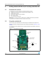
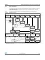
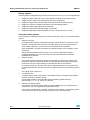
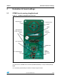
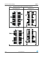
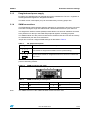
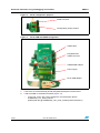
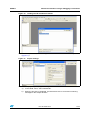
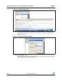
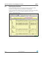
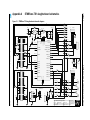
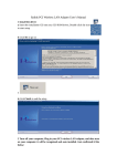
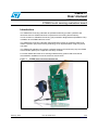
UM0671
User manual
STM8/128-EV/TS
STM8S touch sensing evaluation board
Introduction
The STM8S touch sensing evaluation kit (STM8/128-EV/TS) provides a platform that
introduces users to STMicroelectronics capacitive touch sensing firmware library.
The kit contains an STM8S touch sensing (TS) evaluation daughterboard (STM8Sxxx-TS1)
in addition to the STM8/128-EVAL board.
The STM8S touch sensing evaluation daughterboard provides an evaluation platform for
resistor-capacitor (RC) touch sensing technology for an implementation using 5 keys and
one slider.
The STM8S TS evaluation kit provides a software solution for transforming any 8-bit STM8
microcontroller (MCU) into a capacitive touchkey controller.
For further details about the touch sensing software library, please read the technical
documentation available on www.st.com/touch-sense-sw-lib.
Figure 1.
February 2010
STM8S touch sensing evaluation kit
Doc ID 15330 Rev 4
1/23
www.st.com
Contents
UM0671
Contents
1
Overview . . . . . . . . . . . . . . . . . . . . . . . . . . . . . . . . . . . . . . . . . . . . . . . . . . 3
2
Getting started with the touch sensing evaluation kit . . . . . . . . . . . . . . 4
3
2.1
Evaluation kit contents . . . . . . . . . . . . . . . . . . . . . . . . . . . . . . . . . . . . . . . . 4
2.2
Using the evaluation kit . . . . . . . . . . . . . . . . . . . . . . . . . . . . . . . . . . . . . . . 4
2.3
User interface . . . . . . . . . . . . . . . . . . . . . . . . . . . . . . . . . . . . . . . . . . . . . . . 5
Evaluation kit board settings . . . . . . . . . . . . . . . . . . . . . . . . . . . . . . . . . . 7
3.1
3.2
4
STM8S touch sensing daughterboard . . . . . . . . . . . . . . . . . . . . . . . . . . . . 7
3.1.1
Dielectric . . . . . . . . . . . . . . . . . . . . . . . . . . . . . . . . . . . . . . . . . . . . . . . . . 8
3.1.2
Daughterboard MCU pin functions . . . . . . . . . . . . . . . . . . . . . . . . . . . . . 8
3.1.3
Daughterboard power supply . . . . . . . . . . . . . . . . . . . . . . . . . . . . . . . . . 11
3.1.4
SWIM connections . . . . . . . . . . . . . . . . . . . . . . . . . . . . . . . . . . . . . . . . . 11
3.1.5
Analysis connectors (J2 and J3) . . . . . . . . . . . . . . . . . . . . . . . . . . . . . . 12
3.1.6
External supply and communication . . . . . . . . . . . . . . . . . . . . . . . . . . . 12
STM8S2xx evaluation motherboard settings . . . . . . . . . . . . . . . . . . . . . . 13
Advanced evaluation using a debugging environment . . . . . . . . . . . . 15
4.1
Running the evaluation firmware in debug mode . . . . . . . . . . . . . . . . . . . 15
4.2
Entering debug mode using RLink . . . . . . . . . . . . . . . . . . . . . . . . . . . . . . 15
4.3
Exploring key structures . . . . . . . . . . . . . . . . . . . . . . . . . . . . . . . . . . . . . . 20
Appendix A STM8Sxxx-TS1 daughterboard schematics . . . . . . . . . . . . . . . . . . 21
Revision history . . . . . . . . . . . . . . . . . . . . . . . . . . . . . . . . . . . . . . . . . . . . . . . . . . . . 22
2/23
Doc ID 15330 Rev 4
UM0671
1
Overview
Overview
This solution enables designers, comfortable with the use of standard microcontrollers, to
create higher-end “look and feel” user interfaces by replacing conventional electromechanical switches with touch sensing controls.
Designers can combine touch sensing functions with traditional MCU features
(communication, LED control, beeper, LCD control, etc.).
The touch sensing firmware library is part of the application firmware.
Maturity, robustness, flexibility and performance make this solution simple to implement with
a low “time to market” period making it easy to develop all types of applications including
mobile phones, cooking appliances and printers only to name a few.
The STM8S TS evaluation kit comes pre-programmed with evaluation firmware that
manages 5 touch keys and one slider all available on the touch sensing daughterboard.
Using this kit, the user can easily evaluate the touch sensing software features and
performances by monitoring sensing parameters using an LCD display interface.
In development mode, designers are able to debug, modify, adapt or integrate the touch
sensing library in application firmware using a USB debugging and programming tools:
●
Raisonance RLink debugger/programmer for ST microcontrollers
●
STice in-circuit emulation system
●
ST MCU Toolset with ST Visual Develop (STVD) IDE and ST Visual Programmer
(STVP) programming interface
Doc ID 15330 Rev 4
3/23
Getting started with the touch sensing evaluation kit
UM0671
2
Getting started with the touch sensing evaluation kit
2.1
Evaluation kit contents
The STM8S touch sensing evaluation kit (STM8/128-EV/TS) contains:
●
STM8S touch sensing evaluation daughterboard (STM8Sxxx-TS1)
●
STM8/128-EVAL board
●
AC/DC power supply and its AC adaptors
●
MCU selection guide
●
User manual (this document)
IMPORTANT: The STM8 TS library, STM8 Toolset, STM8S firmware library and related
documentation are available at www.st.com/touch-sense-sw-lib
2.2
Using the evaluation kit
After connecting the motherboard to the mains supply, the evaluation kit is ready for use.
Just use the joystick to navigate through the menu options as described in Section 2.3: User
interface.
The evaluation firmware enables the user to quickly evaluate the main features of the touch
sensing library.
Figure 2.
TS evaluation kit assembly
Daughterboard
Motherboard
Pre-programmed
STM8S sample
SWIM connector
Exit sub-menu
Scroll right
Scroll left
Enter sub-menu
LCD display
Power supply
Joystick
Reset
4/23
Doc ID 15330 Rev 4
UM0671
Getting started with the touch sensing evaluation kit
2.3
User interface
The joystick is the main user interface used to display keys values and state or to modify the
main touch sensing library parameters: de-bounce filter, detection time-out, low power
mode, DES setting, etc.
Note:
The 5 touch sensing keys are also for navigating through the touch sensing menu.
Figure 3.
Navigation scheme
Menu entry point
**Menu**
Help push
down (1)
**Menu**
Key info
**Menu**
Detect
TIMEOUT
Exit sub-menu
Scroll left
**Menu**
De-bounce
Filter
**Menu**
Low Power
Mode
**Menu**
DES Setting
Detect
TIMEOUT
00 sec
Scroll right
De-bounce
Filter
3
1
Enter sub-menu
2
Low Power
Mode
128 mSec
Parameter
setting
sub-menus
3
DES Setting
Disable
4
**Menu**
Sel Key
summary
**Menu**
About
**Menu**
Select Key X
K1 K2 K3 K4 K5
Slider Bar: = = = = = = = =
STATE Key X
Idle or Detected
1
2
STM8S Touch
Eval Vx.x.x
**Menu**
Select slider
KeyX Sig=0x0184
KeyX Ref=0x015E
3
Noise rejection
Counter KeyX
0000
Slider STATE
Idle or Detected
4
5
Counter
RESET
S Sig=0x92
S Pos=0x09
6
S Resolution
x bits
7
Display
sub-menus
Decrement
Resolution
< Resolution <
x bits
Increment
Resolution
1. After power on, to quickly display the key and slider states (display option 1), move the joystick once to the right (→) and
twice towards the bottom (↓).
Doc ID 15330 Rev 4
5/23
Getting started with the touch sensing evaluation kit
UM0671
Display options
Use the joystick to navigate through the sub-menus as shown in Figure 3 to do the following:
1.
Display the state of keys (K1, K2, K3, K4 and K5) and slider on the same screen.
2.
Display only the state of the selected key (Kx) (Idle or Detected).
3.
Display the signal value and the reference threshold of the selected Key (Kx).
4.
Display the number of samples rejected by the noise filtering system.
5.
Display the state of the slider (Idle or Detected).
6.
Display the signal value and the position of the slider.
7.
Display/change slider resolution (default is 4 bits, may be set to up to 7 bits).
Parameter setting options
Use the joystick to navigate through the sub-menus as shown in Figure 3 to set the following
options:
1.
Detection time-out
This feature automatically recalibrates keys after a fixed duration of continuous touch
detection. This prevents the keys from becoming 'stuck on' due to foreign objects or
other sudden influences. This is known as the detection time-out feature.
After recalibration, the keys will continue to operate normally, even if partially or fully
obstructed.
Infinite timeout (detection time-out value = 0) is useful in applications where a
prolonged detection can occur and where the output must reflect the detection
regardless of its duration.
2.
De-bounce filter
The de-bounce filter reduces the effects of low frequency noise on key states. This
mechanism requires a specified number of measurements that qualify as detections
(and these must occur consecutively) or the detection will not be reported.
In a similar manner, the end of a touch (loss of signal) also has to be confirmed over
several measurements. This process acts as a type of “de-bounce” mechanism against
noise.
The typical value is equal to 2.
3.
Low power mode
To reduce device power consumption, this feature inserts a low power mode window
between each key acquisition period.
This window duration is programmable with the following typical values (in
milliseconds): 0, 1, 2, 4, 8, 16, 32, 64, and 128.
4.
Detection Exclusion System
The Detection Exclusion System (DES) prevents multiple keys from responding to a
single touch. This can happen with closely spaced keys.
Once a key is considered as “touched”, all other keys are locked in an untouched state.
To unlock these keys, the touched key must return to an untouched state.
6/23
Doc ID 15330 Rev 4
UM0671
Evaluation kit board settings
3
Evaluation kit board settings
3.1
STM8S touch sensing daughterboard
Figure 4.
STM8S TS daughterboard overview
1 selection key
4 direction keys
Slider
Connectors to
STM8/128-EVAL
board
Analysis
connectors
I2C connector
STM8S MCU
SWIM
connector
and jumper
IDD measurement
STM8S MCU
This board uses a STM8S microcontroller (STM8S207K6T6C) in a 32-pin LQFP package.
Keys
The 5 touchkeys (electrodes) are made of a simple copper surface.
Doc ID 15330 Rev 4
7/23
Evaluation kit board settings
UM0671
Slider
The slider consists of 5 elementary juxtaposed electrodes.
Analysis connectors
All electrode and driven shield signals are available through two connectors (J2 and J3) for
analysis and monitoring.
I2C communication connector
In the event of I2C communication, the daughterboard provides a connector (J6) for the I2C
data and clock signals for interfacing with the STM8S microcontroller.
SWIM connector and setting jumper
A single-wire interface module (SWIM) interface (J5) with its associated jumper (W1) for
analysis and development.
3.1.1
Dielectric
A 1.5-mm thick Plexiglas panel (Figure 5) is used as a dielectric between the electrodes and
the touch surface. The user can replace this panel by another kind of dielectric with a
different thickness and/or material. Consequently, new firmware parameters will have to be
tuned.
Figure 5.
Interchangeable dielectric panel
Screw holes
3.1.2
Daughterboard MCU pin functions
Table 1 describes the application functions assigned to each pin of the daughterboard
microcontroller.
The motherboard provides certain resources for the daughterboard such as the LCD, power
supply, LEDs, joystick, buzzer, etc.
For more information, see Section 3.2: STM8S2xx evaluation motherboard settings.
Table 1.
Pin no.
8/23
Daughterboard MCU pin description
Pin name
Application usage
1
RST
2
PA1
LED4
3
PA2
Backlight
Option
Disconnect
Doc ID 15330 Rev 4
Configuration
R17
UM0671
Evaluation kit board settings
Table 1.
Pin no.
Note:
Daughterboard MCU pin description (continued)
Pin name
Application usage
Option
Configuration
4
VSS
5
VCAP
6
VDD
7
VDDIO_1
8
PF4
9
VDDA
10
VSSA
11
PB5
LED2
I²C SDA
R43
12
PB4
LED3
I²C SCL
R42
13
PB3
Joy Down
14
PB2
Joy Left
15
PB1
Joy Right
16
PB0
Joy Up
17
PE5
LCD CS
18
PC1
Key K1
19
PC2
Key K2
20
PC3
Key K3
21
PC4
Buzzer
Driven shield keys
R4/R46
22
PC5
SPI SCK
23
PC6
SPI MOSI
24
PC7
Key K4
25
PD0
Key K5
26
PD1
DB SWIM connector
MB SWIM connector
W1
27
PD2
Slider S5
28
PD3
Slider S4
29
PD4
Slider S3
30
PD5
Slider S2
31
PD6
Slider S1
32
PD7
Driven shield slider
LED1
R45/R44
Load
Options are selected using 0-ohm resistors.
Doc ID 15330 Rev 4
9/23
Evaluation kit board settings
Table 2.
UM0671
Daughter/motherboard CN1 and CN5 header connections
Motherboard connector
(STM8/128-EVAL board)
Daughterboard connector
(STM8S2Kxxx-TS1)
CN1 header
PG2
PG0
PC6
PC4
PC3
PC1
PE5
PE7
PH5
PI7
PE0
PE2
PE4
D5V
2
4
6
8
10
12
14
16
18
20
22
24
26
28
30
32
34
36
38
40
42
44
46
48
50
PD1
PD3
PD5
PG6
PI5
PI3
PI1
PG4
PG3
PG1
PC7
PC5
RST R41
D5V
PB4
PD7
PC2
PC0
PE6
PH7
PH6
PH4
PB3
PB2
+3V3
1
3
5
7
9
11
13
15
17
19
21
23
25
27
29
31
33
35
37
39
41
43
45
47
49
PI6
PE1
PE3
PG7
PG5
PI4
PI2
PI0
J1 header
R16
820
PA2
PA4
PA6
D5V
PB4
PB2
PB0
1
3
5
7
9
11
13
15
17
19
21
23
25
27
29
31
33
35
37
39
41
43
45
47
49
2 on the left
PD1
PD3
PD5
PD7
PH1
PH3
PF6
PF5
PF3
PF1
PB7
10/23
2
4
6
8
10
12
14
16
18
20
22
24
26
28
30
32
34
36
38
40
42
44
46
48
50
PD0
PD2
PD4
PD6
PB5
PF4
PE5
PB0
PB1
Header 25X2
J4 header
CN5 header
RESET#
1
3
5
7
9
11
13
15
17
19
21
23
25
27
29
31
33
35
37
39
41
43
45
47
49
2
4
6
8
10
12
14
16
18
20
22
24
26
28
30
32
34
36
38
40
42
44
46
48
50
PD0
PD2
PD4
PD6
PA0
PA1
PA3
PA5
PC6
PC4
PC3
PH0
PH2
PF7
PF4
PF2
PF0
PB6
PB5
PB3
PB1
PC1
D5V
1
3
5
7
9
11
13
15
17
19
21
23
25
27
29
31
33
35
37
39
41
43
45
47
49
2
4
6
8
10
12
14
16
18
20
22
24
26
28
30
32
34
36
38
40
42
44
46
48
50
Header 25X2
Doc ID 15330 Rev 4
PC7
PC5
PC2
PA2 +3.3V
UM0671
3.1.3
Evaluation kit board settings
Daughterboard power supply
By default, the daughterboard is powered through the motherboard. The 3.3 V regulator on
the daughterboard supplies the daughterboard MCU.
The MCU current consumption (IDD) can be measured by removing jumper W2.
3.1.4
SWIM connections
The STM8 debug system interface allows a debugging or programming tool to be connected
to the MCU through a single-wire bidirectional communication based on open-drain line.
This single-wire interface module (SWIM) module allows non-intrusive read/write accesses
to be performed on-the-fly to the RAM and peripheral registers, for debug purposes.
The SWIM module can also perform a MCU device software reset and can also be used by
as a standard I/O port with some restrictions.
Jumper W1 is used to configure SWIM settings as described in Table 3.
Table 3.
W1 jumper description
Configuration
1
2
3
1
2
3
Description
Uses STM8S TS daughterboard SWIM connector (default setting)
Connect PD1of STM8S TS daughterboard device to resource of STM8S/128EVAL board.
For more information, please refer to user manual UM0470: STM8 SWIM communication
protocol and debug module.
Figure 6.
SWIM connector (top view)
1
Table 4.
3
4
SWIM connector pin description
Pin number
Note:
2
Description
Pin number
Description
1
VDD
2
PD1
3
GND
4
PA0 (RESET)
The SWIM connector of the STM8/128-EVAL board cannot be used.
Doc ID 15330 Rev 4
11/23
Evaluation kit board settings
3.1.5
UM0671
Analysis connectors (J2 and J3)
Application designers can use connectors J2 and J3 to analyze electrode and driven shield
signals on the daughterboard.
Note:
The user should take into account possible probe capacitance disturbance and should
consider re-calibrating the device before use.
Table 5.
J2 connector pin description
Pin number
Shield
Description
Description
Slider 1 active shield
K3
Key 3 electrode
K1
Key 1 electrode
K4
Key 4 electrode
K2
Key 2 electrode
K5
Key 5 electrode
Table 6.
J3 connector pin description
Pin number
3.1.6
Pin number
Description
Pin number
Description
S1_1
Slider 1 electrode 1
S1_4
Slider 1 electrode 4
S1_2
Slider 1 electrode 2
S1_5
Slider 1 electrode 5
S1_3
Slider 1 electrode 3
Shield
Slider 1 active shield
External supply and communication
Connector J6 provides I2C data and clock signal pins for communication with the
daughterboard microcontroller. The user can use these pins to develop his own
communication protocol.
Resistors R36 and R37 are available as I2C pull-up resistors and can be mounted by the
user if needed.
Note:
If the device is supplied by pin 1 and 5, jumper W2 must not be connected.
Table 7.
J6 connector pin description
Pin number
Description
Pin number
Description
2
1
VSS
4
I C SDA
2
PA1
5
VDD
3
I2C SCL
Pin 2 is connected to PA1 and is available for user implementation. For example, it may be
used for acquisition synchronization.
12/23
Doc ID 15330 Rev 4
UM0671
3.2
Evaluation kit board settings
STM8S2xx evaluation motherboard settings
Figure 7.
TS motherboard overview
CN5 header
CN1 header
Jumper JP1
Jumper JP3
LCD display
Power supply
Reset
Joystick
When using the STM8S TS daughterboard assembled with the STM8/128-EVAL (mother)
board, the following settings must be implemented:
●
To maintain STM8S TS daughterboard MCU functionality, the Reset Source (JP1)
jumper must be set to the “STice” position (Table 8) on the STM8/128-EVAL board.
●
To supply power from the supply jack (CN6) to both mother and daughterboards
connected on connectors CN5 and CN1:
–
On STM8S TS daughterboard, connect both pins on jumper W2 (Section 3.1.3).
–
On STM8/128-EVAL board, set jumper JP3 as shown in Table 8. (STM8S TS
daughterboard must have not its own power supply connected.)
For more information about the STM8/128-EVAL board, please refer to UM0482: STM8/128EVAL evaluation board user manual.
Doc ID 15330 Rev 4
13/23
Evaluation kit board settings
Table 8.
UM0671
STM8/128-EVAL board settings
Description
JP1
Set to “STice” to keep motherboard MCU Reset pin low to enable
correct TS daughterboard MCU functionality. (Default configuration)
JP3
Connect both PSU and DTB jumpers to supply power supply the TS
daughterboard. (Default configuration)
Configuration
1
DTB
Jumper
PSU
14/23
Doc ID 15330 Rev 4
2
3
1
2
1
2
UM0671
Advanced evaluation using a debugging environment
4
Advanced evaluation using a debugging environment
4.1
Running the evaluation firmware in debug mode
Designers can easily run the evaluation firmware in Debug mode using ST debugging and
programming tools.
●
●
Hardware tools to be ordered separately:
–
Raisonance RLink debugger/programmer for ST microcontrollers
(www.raisonance.com/)
–
STice in-circuit emulation system
Software tools to be downloaded separately:
–
ST MCU Toolset with ST Visual Develop (STVD) IDE and ST Visual Programmer
(STVP) programming interface
–
STM8 Cosmic C compiler (www.cosmic-software.com/)
In Debug mode, designers can perform an in-depth evaluation of the firmware and visualize
touch sensing parameters. Designers can even customize the touch sensing library to their
specific needs by creating their own application firmware.
For further information about ST software, STM8 microcontrollers or debugging tools,
please read the associated documentation or ask your local ST support team for a training
session. More information is available at www.st.com/touch-sense-sw-lib
4.2
Entering debug mode using RLink
This section describes the steps necessary to set up a platform for evaluating and
developing TS firmware.
Note:
For links to tools and downloads, please refer to ST’s microcontroller web site at
www.st.com/mcu/.
1.
Download and install the ST MCU Toolset with ST Visual Develop (STVD) IDE and ST
Visual Programmer (STVP) programming interface (one single download).
2.
3.
Download and install the STM8 cosmic C compiler.
Install the Rlink USB driver using one of the two following methods:
–
Insert the RAISONANCE CD-ROM into your CD drive and exit from Autorun.
Explore the CD-ROM contents and execute the RLinkUSBInstall.exe file in the
D:\Driver\RlinkDrv directory.
–
Download the RLinkUSBInstall.exe file from the Raisonance web site and execute
the file.
Restart your computer to apply these changes.
Install the RLink hardware:
a) Place jumpers on the “SWIM” and “ADAPT” RLink configuration pins of the Rlink
USB adaptor as shown in Figure 8.
b) Connect the SWIM-STM8 adaptor to the RLink USB adaptor.
c) Connect the SWIM cable between the touch sensing daughterboard (J5 SWIM
connector) and the SWIM-STM8 adaptor as shown in Figure 9.
d) Connect the USB cable between your PC and the RLink USB adaptor.
e) Power the TS daughterboard through the STM8S2xx evaluation board.
4.
5.
Doc ID 15330 Rev 4
15/23
Advanced evaluation using a debugging environment
Figure 8.
UM0671
RLink configuration jumpers
SWIM connector
Configuration jumper location
Figure 9.
RLink USB and SWIM configuration
SWIM cable
Daughterboard
SWIM connector
SWIM/STM8 adaptor
Power supply
RLink USB adaptor
6.
Download the STM8 touch sensing library from www.st.com/touch-sense-sw-lib
7.
Launch the ST Visual Develop (STVD) integrated development environment.
8.
Load the STM8 TS evaluation firmware (Figure 10):
–
In the “File” menu, click “Open workspace” and select/open the file
STM8S20xK_TS1_EVAL_FW.stw.
(Default path file @ \STM8S20xK_TS1_EVAL_FW\Project\STVD\Cosmic)
16/23
Doc ID 15330 Rev 4
UM0671
Advanced evaluation using a debugging environment
Figure 10. Loading the TS evaluation firmware
9.
In the “Project” menu, select “Setting” to define the C cosmic location directory
(Figure 11).
Figure 11. Project settings
10. Build the project by compiling and linking all the source code.
a)
In the “Build” menu, select “Rebuild all”.
b)
When the process is completed, check that there are no errors and no warning
messages in the Output windows.
Doc ID 15330 Rev 4
17/23
Advanced evaluation using a debugging environment
UM0671
Figure 12. Building the project
11. Select RLink as the debugging tool.
–
In the “Debug instrument” menu, click “Target setting” and select “SWIM RLink” as
shown in Figure 13.
Figure 13. Debug instrument settings
12. Start the debugging process.
–
18/23
In the “Debug” menu, select “Start debugging” and click “Run” (or press CTRL-F5)
to start the application in Debug mode.
Doc ID 15330 Rev 4
UM0671
Advanced evaluation using a debugging environment
Figure 14. Debug mode
Doc ID 15330 Rev 4
19/23
Advanced evaluation using a debugging environment
4.3
UM0671
Exploring key structures
All key and slider data structures can be monitored through the STVD watch window.
The main “touch sensing” structures are “sSCKeyInfo” and “sMCKeyInfo”.
To learn more about library variables and function descriptions, please refer to the CHM file
available at <installation path>\STM8_TS_LIB\stm8_tsl_um.chm
Figure 15. STVD watch window
20/23
Doc ID 15330 Rev 4
STM8Sxxx-TS1 daughterboard schematics
UM0671
Appendix A
Figure 16. STM8Sxxx-TS1 daughterboard schematic diagram
R45
SH_DRV
0R_0603
R1
VDD_MCU
VDD
3
CE
C7
4
NC
C8
JUMPER
2.2µF_X5R_0603
2
1µF_X5R_0603
LP2980ABM3-TR
C9
VDD
J1
0R_0603
PC6
PC3
PC1
D5V
PD2
0R_0603/DNF
Shield
9
VDDA
VDDIO_1
PD6/LINUART_RX
PA1/OSCIN
PD5/LINUART_TX
PA2/OSCOUT
PD4/TIM2_CC1/BEEP
R43
PD3/TIM3_CC2
0R_0603
LOAD
8
R20
PF4/AIN12
PD2/TIM3_CC1
0R_603/DNF
PD1/SWIM
PE5
PB0
PB1
PD0/TIM3_CC2
I²C SDA 11
I²C SCL 12
PB3 13
PB1 15
PB0 16
10K_1%_0603
3.3M_1%_0603
R6
31
R7
10K_1%_0603
30
3.3M_1%_0603
R8
R9
10K_1%_0603
3.3M_1%_0603
R10
28
R11
10K_1%_0603
27
3.3M_1%_0603
R12
29
10K_1%_0603
26 SWIM
R13
25
SH_DRV
10K_1%_0603
PB4/AIN4
PC7/SPI_MISO
R38
0R_1%_0603
PB3/AIN3
PC6/SPI_MOSI
PB2/AIN2
PC5/SPI_SCK
PB1/AIN1
PC4/TIM1_CC4
PB0/AIN0
PC3/TIM1_CC3
PE5/SPI_NSS
PC1/TIM1_CC1
24
23 PC6
22 PC5
J3
R47
21
0R_0603/DNF
20
18
PD0
R21
PC7
R25
PC3
R28
0R_0603/DNF
W1
JUMPER 3 POS
PC2
VDD
0R_0603/DNF
J5
PA2 +3.3V
G1
SWIM
VDD
4 RST
3
2
1
R37
J6
PD1
SWIM
5
4
3
2
1
21/23
Header 5
I²C SCL
I²C SDA
PA1
Header 6
19
PC7
PC5
VDD
Shield
C10
1nF_X7R_0603
0R_0603/DNF
GND
RST
GND
SWIM
VDD
GND
1
2
3
4
5
Slider
Shield
R22
G2
S1
PB5/AIN5
PC2/TIM1_CC2
PE5 17
R5
32
R40
7
5
6
VDD
PD7/TLI
0R_0603/DNF
3
0R_0603
R3
R39
PA2
R17
2
3.3M_1%_0603
1
2
3
4
5
6
PA1
J4
Header 25X2
RST
10nF_X7R_0603
PB2 14
2
4
6
8
10
12
14
16
18
20
22
24
26
28
30
32
34
36
38
40
42
44
46
48
50
VCAP
1
Header 25X2
1
3
5
7
9
11
13
15
17
19
21
23
25
27
29
31
33
35
37
39
41
43
45
47
49
PD3
0R_0603/DNF
R19
R36
4.7K_1%_0603/DNF
R46
RST
4.7K_1%_0603/DNF
PB2
PD4
0R_0603/DNF
R18
STM8S208K3T
VSSA
PB3
C3
U1
10K_1%_0603
VSS
0R_0603/DNF
R16
C1
PC2
R30
0R_0603/DNF
PC1
R32
1M_1%_0603
R23
R24
10K_1%_0603
1M_1%_0603
R26
Title:
R27
10K_1%_0603
R29
R31
10K_1%_0603
1M_1%_0603
R33
R34
10K_1%_0603
1M_1%_0603
R35
Reference: MB836
Date: 06-Nov-09
K3
1
K2
1
K1
1
10K_1%_0603
STM8SxxxK-TS1 Daughter Board
Size: A4
K4
1
1M_1%_0603
0R_0603/DNF
Revision: C-01
Sheet: 1
of 1
K5
1
STMicroelectronics
Microcontrollers Division
190, avenue Célestin COQ
13106 ROUSSET Cedex
FRANCE
STM8Sxxx-TS1 daughterboard schematics
Doc ID 15330 Rev 4
R44
C2
10
D5V
680nF_X5R_0603
R4
4
0R_0603
C4
Header 6
R2
1
0R_0603
R42
PD0
PD2
PD4
PD6
2
RST R41
2
4
6
8
10
12
14
16
18
20
22
24
26
28
30
32
34
36
38
40
42
44
46
48
50
3
PD1
PD3
PD5
1
3
5
7
9
11
13
15
17
19
21
23
25
27
29
31
33
35
37
39
41
43
45
47
49
J2
PD5
0R_0603/DNF
1
2
3
4
5
6
100nF_X7R_0603
100nF_X7R_0603
C6
5
Vout
100nF_X7R_0603
C5
100nF_X7R_0603
Vin
GND
1
PD6
0R_0603/DNF
R15
W2
0R_0603/DNF
0R_0603/DNF
U2
100nF_X7R_0603
D5V
R14
Revision history
UM0671
Revision history
Table 9.
22/23
Document revision history
Date
Revision
Changes
04-Feb-2009
1
Initial release.
09-Mar-2009
2
Updated Figure 3: Navigation scheme on page 5 and Display options
on page 6.
20-Mar-2009
3
Corrected reference to STM8S touch sensing evaluation kit from
“STM8/128-EVAL/TS” to “STM8/128-EV/TS”.
26-Feb-2010
4
Updated values of C3 and C9 in Figure 16 on page 21.
Doc ID 15330 Rev 4
UM0671
Please Read Carefully:
Information in this document is provided solely in connection with ST products. STMicroelectronics NV and its subsidiaries (“ST”) reserve the
right to make changes, corrections, modifications or improvements, to this document, and the products and services described herein at any
time, without notice.
All ST products are sold pursuant to ST’s terms and conditions of sale.
Purchasers are solely responsible for the choice, selection and use of the ST products and services described herein, and ST assumes no
liability whatsoever relating to the choice, selection or use of the ST products and services described herein.
No license, express or implied, by estoppel or otherwise, to any intellectual property rights is granted under this document. If any part of this
document refers to any third party products or services it shall not be deemed a license grant by ST for the use of such third party products
or services, or any intellectual property contained therein or considered as a warranty covering the use in any manner whatsoever of such
third party products or services or any intellectual property contained therein.
UNLESS OTHERWISE SET FORTH IN ST’S TERMS AND CONDITIONS OF SALE ST DISCLAIMS ANY EXPRESS OR IMPLIED
WARRANTY WITH RESPECT TO THE USE AND/OR SALE OF ST PRODUCTS INCLUDING WITHOUT LIMITATION IMPLIED
WARRANTIES OF MERCHANTABILITY, FITNESS FOR A PARTICULAR PURPOSE (AND THEIR EQUIVALENTS UNDER THE LAWS
OF ANY JURISDICTION), OR INFRINGEMENT OF ANY PATENT, COPYRIGHT OR OTHER INTELLECTUAL PROPERTY RIGHT.
UNLESS EXPRESSLY APPROVED IN WRITING BY AN AUTHORIZED ST REPRESENTATIVE, ST PRODUCTS ARE NOT
RECOMMENDED, AUTHORIZED OR WARRANTED FOR USE IN MILITARY, AIR CRAFT, SPACE, LIFE SAVING, OR LIFE SUSTAINING
APPLICATIONS, NOR IN PRODUCTS OR SYSTEMS WHERE FAILURE OR MALFUNCTION MAY RESULT IN PERSONAL INJURY,
DEATH, OR SEVERE PROPERTY OR ENVIRONMENTAL DAMAGE. ST PRODUCTS WHICH ARE NOT SPECIFIED AS "AUTOMOTIVE
GRADE" MAY ONLY BE USED IN AUTOMOTIVE APPLICATIONS AT USER’S OWN RISK.
Resale of ST products with provisions different from the statements and/or technical features set forth in this document shall immediately void
any warranty granted by ST for the ST product or service described herein and shall not create or extend in any manner whatsoever, any
liability of ST.
ST and the ST logo are trademarks or registered trademarks of ST in various countries.
Information in this document supersedes and replaces all information previously supplied.
The ST logo is a registered trademark of STMicroelectronics. All other names are the property of their respective owners.
© 2010 STMicroelectronics - All rights reserved
STMicroelectronics group of companies
Australia - Belgium - Brazil - Canada - China - Czech Republic - Finland - France - Germany - Hong Kong - India - Israel - Italy - Japan Malaysia - Malta - Morocco - Philippines - Singapore - Spain - Sweden - Switzerland - United Kingdom - United States of America
www.st.com
Doc ID 15330 Rev 4
23/23