1
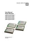
User Manual
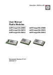
Radio Modules
deRFmega128-22A00
deRFmega128-22A02
deRFmega128-22C00
deRFmega128-22C02
Document Version V01.03
2010-09-07
User Manual
Version 01.03
2010-09-07
Radio modules deRFmega128
Table of contents
1.
Overview ......................................................................................................................... 5
2.
Application....................................................................................................................... 5
3.
Features.......................................................................................................................... 6
4.
Technical data................................................................................................................. 7
5.
Mechanical size............................................................................................................... 8
5.1. Radio module (pluggable) ...................................................................................... 8
5.2. Footprint receptacles.............................................................................................. 8
5.3. Radio module (solderable) ..................................................................................... 9
5.4. Footprint Pads........................................................................................................ 9
6.
Soldering Profile of deRFmega128-22C00 and deRFmega128-22C02 ......................... 10
7.
Pin assignment.............................................................................................................. 11
8.
Programming................................................................................................................. 17
8.1. Required Hardware .............................................................................................. 17
8.2. JTAG interface ..................................................................................................... 18
9.
Debugging and Tracing ................................................................................................. 19
10. Onboard EEPROM........................................................................................................ 20
11. RF components............................................................................................................. 21
11.1. deRFmega128-22A00 / 22C00............................................................................. 21
11.2. deRFmega128-22A02 / 22C02............................................................................. 22
12. Radio Certification ......................................................................................................... 23
12.1. United States (FCC) ............................................................................................. 23
12.2. European Union (ETSI) ........................................................................................ 24
12.3. Approved antennas .............................................................................................. 25
13. Ordering Information ..................................................................................................... 26
14. Errata ............................................................................................................................ 27
14.1. Serial TWI EEPROM ............................................................................................ 27
dresden elektronik
ingenieurtechnik gmbh
Enno-Heidebroek-Str. 12
01237 Dresden / Germany
Tel.: +49 351 – 31 85 00
Fax: +49 351 – 3 18 50 10
[email protected]
www.dresden-elektronik.de
Page 2 of 28
User Manual
Version 01.03
2010-09-07
Radio modules deRFmega128
Document history
Date
Version
Description
2010-01-25
01.00
Initial version
2010-03-30
01.01
Addition of deRFmega128-22C00
2010-08-25
01.02
Updated deRFmega128-22A00 / -22A02 to Rev02
Addition of deRFmega128-22C02
New pin designation
Updated footprint receptacles
2010-09-07
01.03
Updated Programming section
Mailing list
Firm
Division / Name
DE
Dev. / A. Palm
Author / Check / Release
Author
Firm
Division / Name
DE
Dev. / A. Palm
Check
release
dresden elektronik
ingenieurtechnik gmbh
Enno-Heidebroek-Str. 12
01237 Dresden / Germany
Tel.: +49 351 – 31 85 00
Fax: +49 351 – 3 18 50 10
[email protected]
www.dresden-elektronik.de
Page 3 of 28
User Manual
Version 01.03
2010-09-07
Radio modules deRFmega128
Abbreviations
Abbreviation
Description
ADC
Analog to Digital Converter
BOD
Brownout-Detection
CE
Consumer Electronics
FCC
Federal Communications Commission
GPIO
Generals Purpose Input Output
JTAG
Joint Test Action Group
RF
Radio Frequency
SPI
Serial Peripheral Interface
TWI
Two-Wire Interface
UART
Universal Asynchronous Receiver Transmitter
dresden elektronik
ingenieurtechnik gmbh
Enno-Heidebroek-Str. 12
01237 Dresden / Germany
Tel.: +49 351 – 31 85 00
Fax: +49 351 – 3 18 50 10
[email protected]
www.dresden-elektronik.de
Page 4 of 28
User Manual
Version 01.03
2010-09-07
Radio modules deRFmega128
1. Overview
The pluggable compact radio modules deRFmega128-22A00, deRFmega128-22A02 and the
solderable radio module deRFmega128-22C00 and deRFmega128-22C02 include Atmel’s
Single-Chip ATmega128RFA1, which combines an 8-Bit AVR microcontroller with a 2.4GHz
transceiver.
2. Application
The main applications for the radio modules are:
• 2.4GHz IEEE 802.15.4
• ZigBee® Pro
• ZigBee® RF4CE
• ZigBee® IP
• 6LoWPAN
• ISA SP100
• WirelessHART
• Wireless Sensor Networks (WSN)
• industrial and home controlling and monitoring
dresden elektronik
ingenieurtechnik gmbh
Enno-Heidebroek-Str. 12
01237 Dresden / Germany
Tel.: +49 351 – 31 85 00
Fax: +49 351 – 3 18 50 10
[email protected]
www.dresden-elektronik.de
Page 5 of 28
User Manual
Version 01.03
2010-09-07
Radio modules deRFmega128
3. Features
The radio modules deRFmega128-22A00 and deRFmega128-22C00 offer the following
features:
• Compact size: 30 x 22.7 mm (for 22A00) and 30 x 20.4 mm (for 22C00)
• Pluggable: 2 male connectors, 23 pins per row, 1.27mm pitch
• RF shielding
• Usable signals: power supply, peripheral, programming, debugging, tracing, ADC,
GPIO
• Application interfaces: 2 x UART, 1 x TWI
• Debug/Programming interfaces: 1 x SPI, 1 x JTAG
• Onboard chip-antenna 2.4GHz
• Onboard EEPROM for firmware update over-the-air and/or process data storing
(1Mbit, serial, TWI, onboard Pull-ups on SDA an SCL)
• Certification: CE, FCC
VCC
1,8..3,6V
JTAG
USART/SPI
TWI
EEPROM
128k x 8Bit
ATmega128RF
GPIO
ADC
Chip
antenna
IRQ
Figure 1: block diagram deRFmega128-22A00 / 22C00
The deRFmega128-22A02 and deRFmega128-22C02 offer the same features like the
deRFmega128-22A00 except the chip antenna is replaced by a coaxial receptacle (U.FL) for
connecting an external antenna.
VCC
1,8..3,6V
JTAG
USART/SPI
TWI
EEPROM
128k x 8Bit
ATmega128RF
GPIO
ADC
Coaxial
Connector
IRQ
Figure 2: block diagram deRFmega128-22A02 / 22C02
dresden elektronik
ingenieurtechnik gmbh
Enno-Heidebroek-Str. 12
01237 Dresden / Germany
Tel.: +49 351 – 31 85 00
Fax: +49 351 – 3 18 50 10
[email protected]
www.dresden-elektronik.de
Page 6 of 28
User Manual
Version 01.03
2010-09-07
Radio modules deRFmega128
4. Technical data
Table 1: Mechanical data
Mechanical
Radio modules
Size (L x B )
30 x 22.7 mm (for deRFmega128-22A00 / 22A02)
30 x 20.4 mm (for deRFmega128-22C00 / 22C02)
Connectors
number of headers
pins per header
pitch
pin length
pin diameter
Insulator (L x B x H)
Pins
pitch
2
23
1.27 mm
3.05 mm
0.51 mm
29.2 x 2.5 x2.5 mm
1.27 mm
Table 2: Temperature range
Temperature range
Working range
T_work
Min
-40
Typ
Max
+85
Unit
°C
Min
1.8
Typ
3.3
18
19
6.5
5
1.0
Max
3.6
Unit
VDC
mA
mA
mA
µA
µA
Typ
-0.9
Max
Table 3: Electrical data
Electrical (Vcc = 3,3VDC)
Parameter
Supply Voltage
VCC
Current
I_TXon (TX_PWR = +3dBm)
consumption
I_RXon
I_Idle (Txoff, BOD on)
I_BODon
I_Sleep
(depends on Sleep Mode)
0.5
5
Table 4: RF data
Radio (Vcc = 3,3VDC)
Parameter
Transmit
TX_PWR = 0
power conducted
dresden elektronik
ingenieurtechnik gmbh
Enno-Heidebroek-Str. 12
01237 Dresden / Germany
Min
Tel.: +49 351 – 31 85 00
Fax: +49 351 – 3 18 50 10
[email protected]
www.dresden-elektronik.de
Unit
dBm
Page 7 of 28
User Manual
Version 01.03
2010-09-07
Radio modules deRFmega128
5. Mechanical size
5.1.
Radio module (pluggable)
Used connectors: SAMTEC “TMS-123-02-L-S”
22,7mm
30,0mm
Figure 3: Size deRFmega128-22A00 and deRFmega128-22A02
5.2.
Footprint receptacles
Used receptables: SAMTEC “SLM-123-01-L-S”
0,65mm
20,4mm
1,27mm
Figure 4: Footprint receptacles 1.27mm pitch
dresden elektronik
ingenieurtechnik gmbh
Enno-Heidebroek-Str. 12
01237 Dresden / Germany
Tel.: +49 351 – 31 85 00
Fax: +49 351 – 3 18 50 10
[email protected]
www.dresden-elektronik.de
Page 8 of 28
User Manual
Version 01.03
2010-09-07
5.3.
Radio modules deRFmega128
Radio module (solderable)
20.4mm
30,0mm
Figure 5: Size deRFmega128-22C00 and deRFmega128-22C02
5.4.
Footprint Pads
0.27mm
21.4mm
1.0mm
1.0mm
Figure 6: Footprint for deRFmega128-22C00 and deRFmega128-22C02
Do not place ground areas below the radio module and near the chip-antenna.
dresden elektronik
ingenieurtechnik gmbh
Enno-Heidebroek-Str. 12
01237 Dresden / Germany
Tel.: +49 351 – 31 85 00
Fax: +49 351 – 3 18 50 10
[email protected]
www.dresden-elektronik.de
Page 9 of 28
User Manual
Version 01.03
2010-09-07
Radio modules deRFmega128
6. Soldering Profile of deRFmega128-22C00 and deRFmega128-22C02
Table 5 gives the soldering profile for the radio modules.
Table 5: Soldering Profile
Profile Feature
Average-Ramp-up Rate (217°C to Peak)
Preheat Temperature 175°C ±25°C
Temperature Maintained Above 217°C
Time within 5°C of Actual Peak Temperature
Peak Temperature Range
Ramp-down Rate
Time 25°C to Peak Temperature
Values
3°C/sec max.
180 sec. max
60 sec. to 150 sec.
20 sec. to 40 sec.
260°
6°C/sec max.
8 min. max.
t [s]
Measured Temp.
Zone Temp.
Figure 7: Recorded soldering profile
A solder process without supply of nitrogen causes a discoloration of the metal RF-shielding.
dresden elektronik
ingenieurtechnik gmbh
Enno-Heidebroek-Str. 12
01237 Dresden / Germany
Tel.: +49 351 – 31 85 00
Fax: +49 351 – 3 18 50 10
[email protected]
www.dresden-elektronik.de
Page 10 of 28
360
340
320
300
280
260
240
220
200
180
160
140
120
100
80
60
40
20
280
260
240
220
200
180
160
140
120
100
80
60
40
0
T [°C]
Figure 7 shows a recorded soldering profile for a radio module. The blue colored line
illustrates a temperature sensor placed next to the soldering-contacts of the radio module.
The pink line shows the set temperatures depending on the zone within the reflow soldering
machine.
User Manual
Version 01.03
2010-09-07
Radio modules deRFmega128
7. Pin assignment
Both pin headers respectively pin contacts provide the most important signals to the
customer: power supply, peripheral, programming, debugging, tracing, analog measurement
and free programmable ports. All provided signals except VCC, DGND, RSTN, RSTON,
AREF and CLKI are free programmable port pins (GPIO).
Figure 8: Top overlay deRFmega128-22A00
Figure 9: Top overlay deRFmega128-22A02
dresden elektronik
ingenieurtechnik gmbh
Enno-Heidebroek-Str. 12
01237 Dresden / Germany
Tel.: +49 351 – 31 85 00
Fax: +49 351 – 3 18 50 10
[email protected]
www.dresden-elektronik.de
Page 11 of 28
User Manual
Version 01.03
2010-09-07
Radio modules deRFmega128
Figure 10: Top overlay deRFmega128-22C00
Figure 11: Top overlay deRFmega128-22C02
dresden elektronik
ingenieurtechnik gmbh
Enno-Heidebroek-Str. 12
01237 Dresden / Germany
Tel.: +49 351 – 31 85 00
Fax: +49 351 – 3 18 50 10
[email protected]
www.dresden-elektronik.de
Page 12 of 28
User Manual
Version 01.03
2010-09-07
Radio modules deRFmega128
Table 6: Pin assignment of deRFmega128-22A00 / 22A02 / 22C00 / 22C02
Pin assignment
Pin
µC-Port
1
VCC
2
DGND
3
AREF
4
PG1/DI1
5
RSTN
6
PG2
7
PD0/SCL/INT0
8
PG5/OC0B
9
PD1/SDA/INT1
10
PD3/TXD1/INT3
11
PD7/T0
12
PD5/XCK1
13
PB1/SCK/PCINT1
14
CLKI
15
PB2/MOSI/PCINT2/PDI
16
PB0/SSN/PCINT0
17
PB3/MISO/PCINT3/PDO
18
PB6/OC1B/PCINT6
19
PB4/OC2/PCINT4
20
PB7/OC0A/OC1C/PCINT7
21
PB5/OC1A/PCINT5
22
DGND
23
DGND
Pin
24
25
26
27
28
29
30
31
32
33
34
35
36
37
38
39
40
41
42
43
44
45
46
µC-Port
VCC
DGND
PE0/RXD0/PCINT8
PD2/RXD1/INT2
PE1/TXD0
PD6/T1
PE2/XCK0/AIN0
PE3/OC3A/AIN1
PD4/ICP1
PE4/OC3B/INT4
PF0/ADC0
PE5/OC3C/INT5
PF1/ADC1
PE6/T3/INT6
PF4/ADC4/TCK
PE7/ICP3/CLKO/INT7
PF5/ADC5/TMS
PF2/ADC2
PF6/ADC6/TDO
RSTON
PF7/ADC7/TDI
DGND
DGND
Be careful: with User Manual version 01.02 the pin designation was changed from X1 (1 to
23) and X2 (1 to 23) to an incremental pin numbering from 1 to 46, beginning in the bottom
left corner and move counter-clockwise around the module at top view. There were no
electrical changes made!
dresden elektronik
ingenieurtechnik gmbh
Enno-Heidebroek-Str. 12
01237 Dresden / Germany
Tel.: +49 351 – 31 85 00
Fax: +49 351 – 3 18 50 10
[email protected]
www.dresden-elektronik.de
Page 13 of 28
User Manual
Version 01.03
2010-09-07
Radio modules deRFmega128
Table 7: Description of available I/O port pins
Description of available I/O port pins on header pins
I/O port pin Alternate function (signal name)
Comments
PB0
SSN
PCINT0
PB1
SCK
PCINT1
PB2
MOSI
PDI
PCINT2
PB3
MISO
PDO
PCINT3
PB4
OC2A
PCINT4
PB5
OC1A
PCINT5
PB6
OC1B
PCINT6
PB7
OC0A
OC1C
PCINT7
PD0
SCL
INT0
Onboard Pull-Up Resistor 4k7
PD1
SDA
INT1
Onboard Pull-Up Resistor 4k7
PD2
RXD1
INT2
PD3
TXD1
INT3
PD4
ICP1
PD5
XCK1
PD6
T1
PD7
T0
PE0
RXD0
PCINT8
PE1
TXD0
PE2
XCK0
AIN0
PE3
OC3A
AIN1
PE4
OC3B
INT4
PE5
OC3C
INT5
PE6
T3
INT6
PE7
ICP3
INT7
CLKO
PF0
ADC0
PF1
ADC1
PF2
ADC2
DIG2
PF4
ADC4
TCK
PF5
ADC5
TMS
PF6
ADC6
TDO
PF7
ADC7
TDI
PG1
DIG1
PG2
AMR
PG3
TOSC2
PG4
TOSC1
PG5
OC0B
Note: The I/O port pins PF3/ADC3/DIG4 and PG0/DIG3 are not available!
PG4/TOSC1 and PG3/TOSC2 are connected internal with a 32.768kHz crystal.
dresden elektronik
ingenieurtechnik gmbh
Enno-Heidebroek-Str. 12
01237 Dresden / Germany
Tel.: +49 351 – 31 85 00
Fax: +49 351 – 3 18 50 10
[email protected]
www.dresden-elektronik.de
Page 14 of 28
User Manual
Version 01.03
2010-09-07
Radio modules deRFmega128
Table 8: Signal description list
Signal name
Power
VCC
Function
Type
Voltage Regulator Power Supply
Input
Power
GND
Clocks and Oscillators
CLKI
External Clock Input
CLKO
Divided System Clock Output
JTAG
TCK
Test Clock
TDI
Test Data In
TDO
Test Data Out
TDM
Test Mode Select
Serial Programming
PDI
Data Input
PDO
Data Output
SCK
Serial Clock
Reset
RSTN
Microcontroller Reset
USART
TXD0 – TXD1 Transmit Data
RXD0 – RXD1 Receive Data
XCK0 – XCK1 Serial Clock
Timer/Counter and PWM Controller
OC0A-OC3A
Output Compare and PWM Output
A for Timer/Counter 0 to 3
OC0B-OC3B
Output Compare and PWM Output
B for Timer/Counter 0 to 3
OC0C-OC3C
Output Compare and PWM Output
C for Timer/Counter 0 to 3
T0, T1, T3
Timer/Counter 0,1,3 Clock Input
ICP1
Timer/Counter
Input
Capture
ICP3
Trigger 1 and 3
AMR
Automated Meter Reading
Interrupt
PCINT0 Pin Change Interrupt Source 0 to 7
PCINT7
INT0 – INT7
External Interrupt Input 0 to7
SPI
MISO
SPI Master In/Slave Out
MOSI
SPI Master Out/Slave In
SCK
SPI Bus Serial Clock
SSN
SPI Slave Port Select
dresden elektronik
ingenieurtechnik gmbh
Enno-Heidebroek-Str. 12
01237 Dresden / Germany
Active
Level
Comments
1.8V to 3.6V
Ground
Input
Output
Input
Input
Output
Input
No pull-up resistor
No pull-up resistor
No pull-up resistor
Input
Output
Input
I/O
Low
Pull-Up resistor
Input
Input
Input
Output
Input
I/O
I/O
I/O
I/O
Tel.: +49 351 – 31 85 00
Fax: +49 351 – 3 18 50 10
[email protected]
www.dresden-elektronik.de
Page 15 of 28
User Manual
Version 01.03
2010-09-07
Radio modules deRFmega128
Signal description list (continued)
Signal name
Function
Type
Two-Wire-Interface
SDA
Two-Wire Serial Interface Data
SCL
Two-Wire Serial Interface Clock
Analog-to-Digital Converter
ADC0 – ADC7 Analog to Digital Converter
Channel 0 to 7
AREF
Analog Reference
Analog Comparator
AIN0
Analog Comparator Positive Input
AIN1
Analog Comparator Negative Input
Radio Transceiver
DIG1/DIG2
Antenna Diversity Control Output
dresden elektronik
ingenieurtechnik gmbh
Enno-Heidebroek-Str. 12
01237 Dresden / Germany
I/O
I/O
Active
Level
Comments
Onboard 4k7 Resist.
Onboard 4k7 Resist.
Analog
Analog
Analog
Analog
Output
Tel.: +49 351 – 31 85 00
Fax: +49 351 – 3 18 50 10
[email protected]
www.dresden-elektronik.de
Page 16 of 28
User Manual
Version 01.03
2010-09-07
Radio modules deRFmega128
8. Programming
8.1.
Required Hardware
Dresden elektronik ingenieurtechnik gmbh offers the hardware components for a fast startup. The following hardware setups are possible:
1. Option
•
•
•
•
•
(A) deRFmega128-22A00 or deRFmega128-22A02
(B) deRFtoRCB
(C) Sensor Terminal Board
(D) JTAG-ICE mkII or similar programmer, e.g. AVR Dragon
(E) RS232 Level-Shifter for debugging
(D)
(B)
(C)
(A)
(E)
(E)
Figure 12: Programming option 1
dresden elektronik
ingenieurtechnik gmbh
Enno-Heidebroek-Str. 12
01237 Dresden / Germany
Tel.: +49 351 – 31 85 00
Fax: +49 351 – 3 18 50 10
[email protected]
www.dresden-elektronik.de
Page 17 of 28
User Manual
Version 01.03
2010-09-07
2. Option
•
•
•
•
•
Radio modules deRFmega128
(A) deRFmega128-22A00 or deRFmega128-22A02
(B) deRFtoRCB
(C) JTAG-ICE mkII or similar programmer, e.g. AVR Dragon
(D) JTAG-ICE-Adapter (10 pins, pitch 1.27mm to 30 poles flat cable)
(E) RS232 Level-Shifter for debugging
(C)
(E)
(E)
(D)
(A)
(D)
(B)
Figure 13: Programming option 2
8.2.
JTAG interface
The deRFmega128-22A00 / 22A02 / 22C00 / 22C02 are programmable over JTAG interface
(TDI, TDO, TCK, TMS). If the JTAG-ICE mkII programmer will be used, no external pull-up
resistors are necessary. Use the pin connection shown in Figure 14 to connect the radio
module to a suitable JTAG programmer, for example the JTAG-ICE mkII.
Figure 14: JTAG connector
It is necessary to use the latest version of AVR Studio (min. V4.18 + Service Pack 1 & 2) and
to upgrade the JTAG programmer firmware (min. V06.06; 06.06).
For more details see “deRF Getting Started Web Version” on dresden elektronik homepage.
dresden elektronik
ingenieurtechnik gmbh
Enno-Heidebroek-Str. 12
01237 Dresden / Germany
Tel.: +49 351 – 31 85 00
Fax: +49 351 – 3 18 50 10
[email protected]
www.dresden-elektronik.de
Page 18 of 28
User Manual
Version 01.03
2010-09-07
Radio modules deRFmega128
9. Debugging and Tracing
Debugging and tracing of the radio module is possible with the deRFtoRCB adapter and the
RS232-Level-Shifter. Both components were offered by dresden elektronik ingenieurtechnik
gmbh. The used pin connection is shown in Figure 15 to connect the radio module to a
suitable debug and trace hardware.
Figure 15: Debug interface
For more details see “deRF Getting Started Web Version” on dresden elektronik homepage.
dresden elektronik
ingenieurtechnik gmbh
Enno-Heidebroek-Str. 12
01237 Dresden / Germany
Tel.: +49 351 – 31 85 00
Fax: +49 351 – 3 18 50 10
[email protected]
www.dresden-elektronik.de
Page 19 of 28
User Manual
Version 01.03
2010-09-07
Radio modules deRFmega128
10. Onboard EEPROM
The deRFmega128-22A00 / 22A02 / 22C00 / 22C02 contain a Serial-TWI-EEPROM with a
memory size of 128k x 8Bit.
The EEPROM power supply and the pull-ups will be switched on with a LOW-Signal on port
pin PD6/T1. It is necessary to wait until the TWI interface on the ATmega128RFA1 is
initialized before the communication on the data bus (PD1 and PD0) can be started.
Figure 16: Schematic of EEPROM
dresden elektronik
ingenieurtechnik gmbh
Enno-Heidebroek-Str. 12
01237 Dresden / Germany
Tel.: +49 351 – 31 85 00
Fax: +49 351 – 3 18 50 10
[email protected]
www.dresden-elektronik.de
Page 20 of 28
User Manual
Version 01.03
2010-09-07
Radio modules deRFmega128
11. RF components
11.1. deRFmega128-22A00 / 22C00
The chip antenna on the deRFmega128-22A00 / 22C00 is matched with:
• L1 = 1,0nH (0402)
• L2 = 2,2nH (0402)
Some hints for the positioning of the radio module:
• avoid metallized environments in the near
è mismatching of the antenna
è decreased transmit-range
• place the module at the edge of a device
Figure 17: Matching circuit with chip-antenna
dresden elektronik
ingenieurtechnik gmbh
Enno-Heidebroek-Str. 12
01237 Dresden / Germany
Tel.: +49 351 – 31 85 00
Fax: +49 351 – 3 18 50 10
[email protected]
www.dresden-elektronik.de
Page 21 of 28
User Manual
Version 01.03
2010-09-07
Radio modules deRFmega128
11.2. deRFmega128-22A02 / 22C02
The U.FL coaxial connector on the deRFmega128-22A02 / 22C02 is matched with:
• L2 = 1,0pF (0402)
• C19 = 22pF (0402)
• R1 = 10k (0402)
The deRFmega128-22A02 / 22C02 are suitable for applications in plastic or metal cases.
Figure 18: Matching circuit with U.FL-coaxial-connector
dresden elektronik
ingenieurtechnik gmbh
Enno-Heidebroek-Str. 12
01237 Dresden / Germany
Tel.: +49 351 – 31 85 00
Fax: +49 351 – 3 18 50 10
[email protected]
www.dresden-elektronik.de
Page 22 of 28
User Manual
Version 01.03
2010-09-07
Radio modules deRFmega128
12. Radio Certification
12.1. United States (FCC)
The
deRFmega128-22A00,
deRFmega128-22C00,
deRFmega128-22A02
deRFmega128-22C02 complies with the requirements of FCC part 15.
and
To fulfill FCC Certification requirements, an OEM manufacturer must comply with the
following regulations:
The modular transmitter must be labeled with its own FCC ID number, and, if the FCC ID is
not visible when the module is installed inside another device, then the outside of the device
into which the module is installed must also display a label referring to the enclosed module.
This exterior label can use wording such as the following. Any similar wording that expresses
the same meaning may be used.
Sample label for radio module deRFmega128-22A00 and deRFmega128-22C00:
FCC-ID: XVV-MEGA22A00
This device complies with Part 15 of the FCC Rules. Operation is subject to the following two
conditions: (1) this device may not cause harmful interference, and (2) this device must
accept any interference received, including interference that may cause undesired operation.
Sample label for radio module deRFmega128-22A02 and deRFmega128-22C02:
FCC-ID: XVV-MEGA22A02
This device complies with Part 15 of the FCC Rules. Operation is subject to the following two
conditions: (1) this device may not cause harmful interference, and (2) this device must
accept any interference received, including interference that may cause undesired operation.
Note: The radio modules deRFmega-22C00 and deRFmega-22C02 fulfill a Permissive
Change Class 1 regarding to FCC Section 2.1043 and complies with the requirements of
FCC part 15.
To be used with the deRFmega128-22A02 module, the external antenna have been tested
and approved which is specified in here below. The deRFmega128-22A02 Module may be
integrated with other custom design antennas which OEM installer must authorize following
the FCC 15.21 requirements.
The Original Equipment Manufacturer (OEM) must ensure that the OEM modular transmitter
must be labeled with its own FCC ID number. This includes a clearly visible label on the
outside of the final product enclosure that displays the contents shown below. If the FCC ID
is not visible when the equipment is installed inside another device, then the outside of the
device into which the equipment is installed must also display a label referring to the
enclosed equipment.
This equipment complies with Part 15 of the FCC Rules. Operation is subject to the following
two conditions: (1) this device may not cause harmful interference, and (2) this device must
accept any interference received, including interference that may cause undesired operation
(FCC 15.19). The internal / external antenna(s) used for this mobile transmitter must provide
dresden elektronik
ingenieurtechnik gmbh
Enno-Heidebroek-Str. 12
01237 Dresden / Germany
Tel.: +49 351 – 31 85 00
Fax: +49 351 – 3 18 50 10
[email protected]
www.dresden-elektronik.de
Page 23 of 28
User Manual
Version 01.03
2010-09-07
Radio modules deRFmega128
a separation distance of at least 20 cm from all persons and must not be co-located or
operating in conjunction with any other antenna or transmitter.
Installers must be provided with antenna installation instructions and transmitter operating
conditions for satisfying RF exposure compliance. This device is approved as a mobile
device with respect to RF exposure compliance, and may only be marketed to OEM
installers. Use in portable exposure conditions (FCC 2.1093) requires separate equipment
authorization.
Modifications not expressly approved by this company could void the user's authority to
operate this equipment (FCC section 15.21).
This equipment has been tested and found to comply with the limits for a Class A digital
device, pursuant to Part 15 of the FCC Rules. These limits are designed to provide
reasonable protection against harmful interference when the equipment is operated in a
commercial environment. This equipment generates, uses, and can radiate radio frequency
energy and, if not installed and used in accordance with the instruction manual, may cause
harmful interference to radio communications. Operation of this equipment in a residential
area is likely to cause harmful interference in which case the user will be required to correct
the interference at his own expense (FCC section 15.105).
12.2. European Union (ETSI)
The
deRFmega128-22A00,
deRFmega128-22C00,
deRFmega128-22A02
and
deRFmega128-22C02 modules have been certified for use in European Union countries.
If
the deRFmega128-22A00, deRFmega128-22C00, deRFmega128-22A02 and
deRFmega128-22C02 modules are incorporated into a product, the manufacturer must
ensure compliance of the final product to the European harmonized EMC and lowvoltage/safety standards. A Declaration of Conformity must be issued for each of these
standards and kept on file as described in Annex II of the R&TTE Directive.
The manufacturer must maintain a copy of the deRFmega128-22A00, deRFmega12822C00, deRFmega128-22A02 and deRFmega128-22C02 modules documentation and
ensure the final product does not exceed the specified power ratings, antenna specifications,
and/or installation requirements as specified in the user manual. If any of these specifications
are exceeded in the final product, a submission must be made to a notified body for
compliance testing to all required standards.
The “CE“ marking must be affixed to a visible location on the OEM product. The CE mark
shall consist of the initials "CE" taking the following form:
• If the CE marking is reduced or enlarged, the proportions given in the above
graduated drawing must be respected.
• The CE marking must have a height of at least 5mm except where this is not possible
on account of the nature of the apparatus
• The CE marking must be affixed visibly, legibly, and indelibly.
More detailed information about CE marking requirements you can find at "DIRECTIVE
1999/5/EC OF THE EUROPEAN PARLIAMENT AND OF THE COUNCIL" on 9 March 1999
at section 12.
dresden elektronik
ingenieurtechnik gmbh
Enno-Heidebroek-Str. 12
01237 Dresden / Germany
Tel.: +49 351 – 31 85 00
Fax: +49 351 – 3 18 50 10
[email protected]
www.dresden-elektronik.de
Page 24 of 28
User Manual
Version 01.03
2010-09-07
Radio modules deRFmega128
12.3. Approved antennas
The deRFmega128-22A00 and deRFmega128-22C00 have an integrated chip antenna. The
design is fully compliant with all regulations.
The deRFmega128-22A02 and deRFmega128-22C02 have been tested and approved for
use with the antenna listed below. The module may be integrated with other custom design
antennas which OEM installer must authorize with respective regulatory agencies. The used
antenna was connected to the radio module with a 10cm “U.FL-to-SMA-Reverse pigtail”.
Table 9: Approved antenna(s) and accessory
Approved antenna(s) and accessory
Part
Description
number
BN-023768 Dual-band antenna (2.45GHz
and 5.8GHz) with ReverseSMA-Connector, ¼ wave
BN-023769 U.FL-to-SMA-Reverse pigtail,
10 cm
dresden elektronik
ingenieurtechnik gmbh
Enno-Heidebroek-Str. 12
01237 Dresden / Germany
Manufacturer
Antenna Factor
Hirose /
Profineon
Tel.: +49 351 – 31 85 00
Fax: +49 351 – 3 18 50 10
[email protected]
www.dresden-elektronik.de
Gain
[dBi]
+4,7
Min. Separation
[cm]
20
-0,37
Page 25 of 28
User Manual
Version 01.03
2010-09-07
Radio modules deRFmega128
13. Ordering Information
The product name includes the following information:
deRF xxxx - x x x xx x
Revision
Features
Size
Flash Memory
Frequency Range
Product / Chipset
Table 10: Product name code
Product name code
Information
Product / Chipset
Frequency range
Flash memory
Size
Features
Revision
Code
mega128
1
2
2
A
C
00
02
<blank>
1
2
Explanation
ATmega128RFA1
780/868/915 MHz
2.4 GHz
128 kByte
30 x 22.7 mm
30 x 20.4 mm
chip antenna
coaxial connector
Rev 0
Rev 1
Rev 2
Comments
radio module
pluggable
solderable
onboard
onboard U.FL
Table 11: Ordering information
Ordering information
Part number Product name
BN-028182
deRFmega128-22A00
BN-028498
deRFmega128-22A02
BN-028986
deRFmega128-22C00
BN-028987
deRFmega128-22C02
dresden elektronik
ingenieurtechnik gmbh
Enno-Heidebroek-Str. 12
01237 Dresden / Germany
Comments
pluggable radio module with onboard chip
antenna
pluggable radio module with onboard U.FL
coaxial connector
solderable radio module with onboard chip
antenna
solderable radio module with onboard
U.FL coaxial connector
Tel.: +49 351 – 31 85 00
Fax: +49 351 – 3 18 50 10
[email protected]
www.dresden-elektronik.de
Page 26 of 28
User Manual
Version 01.03
2010-09-07
Radio modules deRFmega128
14. Errata
14.1. Serial TWI EEPROM
Affected devices:
deRFmega128-22A001
deRFmega128-22A021
Problem:
Because of a hardware error the EEPROM, Transistor and Pull-up resistors are not
assembled.
Workaround:
Fixed in revision 2.
Note:
The concerned signals PD0, PD1, PD6 can be used without problems.
dresden elektronik
ingenieurtechnik gmbh
Enno-Heidebroek-Str. 12
01237 Dresden / Germany
Tel.: +49 351 – 31 85 00
Fax: +49 351 – 3 18 50 10
[email protected]
www.dresden-elektronik.de
Page 27 of 28
User Manual
Version 01.03
2010-09-07
Radio modules deRFmega128
dresden elektronik ingenieurtechnik gmbh
Enno-Heidebroek-Straße 12
01237 Dresden
GERMANY
Tel. +49 351 - 31 85 00 | Fax +49 351 - 318 50 10
E-Mail [email protected]
General manager: Dipl.-Ing. L. Pietschmann
Commercial Registry: HRB 749 Dresden Municipal Court
Tax number: 201/107/00726
Sales tax identification number: DE 140125678
Trademarks and acknowledgements
• ZigBee® is a registered trademark of the ZigBee Alliance.
• 802.15.4™ is a trademark of the Institute of Electrical and Electronics Engineers (IEEE).
These trademarks are registered by their respective owners in certain countries only. Other
brands and their products are trademarks or registered trademarks of their respective
holders and should be noted as such.
Disclaimer
This note is provided as-is and is subject to change without notice. Except to the extent
prohibited by law, dresden elektronik ingenieurtechnik gmbh makes no express or implied
warranty of any kind with regard to this guide, and specifically disclaims the implied
warranties and conditions of merchantability and fitness for a particular purpose. dresden
elektronik ingenieurtechnik gmbh shall not be liable for any errors or incidental or
consequential damage in connection with the furnishing, performance or use of this guide.
No part of this publication may be reproduced, stored in a retrieval system, or transmitted in
any form or any means electronic or mechanical, including photocopying and recording, for
any purpose other than the purchaser’s personal use, without the written permission of
dresden elektronik ingenieurtechnik gmbh.
Copyright © 2010 dresden elektronik ingenieurtechnik gmbh. All rights reserved
dresden elektronik
ingenieurtechnik gmbh
Enno-Heidebroek-Str. 12
01237 Dresden / Germany
Tel.: +49 351 – 31 85 00
Fax: +49 351 – 3 18 50 10
[email protected]
www.dresden-elektronik.de
Page 28 of 28