1
STM32F745xx
STM32F746xx
ARM®-based Cortex®-M7 32b MCU+FPU, 462DMIPS, up to 1MB Flash/320+16+ 4KB
RAM, USB OTG HS/FS, ethernet, 18 TIMs, 3 ADCs, 25 com itf, cam & LCD
Datasheet - production data
Features
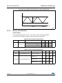
&"'!
®
®
• Core: ARM 32-bit Cortex -M7 CPU with FPU,
adaptive real-time accelerator (ART
Accelerator™) and L1-cache: 4KB data cache
and 4KB instruction cache, allowing 0-wait
state execution from embedded Flash memory
and external memories, frequency up to
216 MHz, MPU, 462 DMIPS/2.14 DMIPS/MHz
(Dhrystone 2.1), and DSP instructions.
• Memories
– Up to 1MB of Flash memory
– 1024 bytes of OTP memory
– SRAM: 320KB (including 64KB of data
TCM RAM for critical real time data) +
16KB of instruction TCM RAM (for critical
real time routines) + 4KB of backup SRAM
(available in the lowest power modes)
– Flexible external memory controller with up
to 32-bit data bus: SRAM, PSRAM,
SDRAM/LPSDR SDRAM, NOR/NAND
memories
• Dual mode Quad SPI
• LCD parallel interface, 8080/6800 modes
• LCD-TFT controller up to XGA resolution with
dedicated Chrom-ART Accelerator™ for
enhanced graphic content creation (DMA2D)
• Clock, reset and supply management
– 1.7 V to 3.6 V application supply and I/Os
– POR, PDR, PVD and BOR
– Dedicated USB power
– 4-to-26 MHz crystal oscillator
– Internal 16 MHz factory-trimmed RC (1%
accuracy)
– 32 kHz oscillator for RTC with calibration
– Internal 32 kHz RC with calibration
• Low-power
– Sleep, Stop and Standby modes
– VBAT supply for RTC, 32×32 bit backup
registers + 4KB backup SRAM
• 3×12-bit, 2.4 MSPS ADC: up to 24 channels
and 7.2 MSPS in triple interleaved mode
• 2×12-bit D/A converters
• Up to 18 timers: up to thirteen 16-bit (1x lowpower 16-bit timer available in Stop mode) and
two 32-bit timers, each with up to 4
IC/OC/PWM or pulse counter and quadrature
(incremental) encoder input. All 15 timers
running up to 216 MHz. 2x watchdogs, SysTick
timer
May 2015
This is information on a product in full production.
LQFP100 (14x14 mm)
LQFP144 (20x20 mm)
LQFP176 (24x24 mm)
LQFP208 (28x28 mm)
UFBGA176 (10x10 mm)
TFBGA216 (13x13 mm)
WLCSP143
(4.5x5.8 mm)
• General-purpose DMA: 16-stream DMA
controller with FIFOs and burst support
• Debug mode
– SWD & JTAG interfaces
– Cortex®-M7 Trace Macrocell™
• Up to 168 I/O ports with interrupt capability
– Up to 164 fast I/Os up to 108 MHz
– Up to 166 5 V-tolerant I/Os
• Up to 25 communication interfaces
– Up to 4× I2C interfaces (SMBus/PMBus)
– Up to 4 USARTs/4 UARTs (27 Mbit/s,
ISO7816 interface, LIN, IrDA, modem
control)
– Up to 6 SPIs (up2to 50 Mbits/s), 3 with
muxed simplex I S for audio class
accuracy via internal audio PLL or external
clock
– 2 x SAIs (serial audio interface)
– 2 × CANs (2.0B active) and SDMMC
interface
– SPDIFRX interface
– HDMI-CEC
• Advanced connectivity
– USB 2.0 full-speed device/host/OTG
controller with on-chip PHY
– USB 2.0 high-speed/full-speed
device/host/OTG controller with dedicated
DMA, on-chip full-speed PHY and ULPI
– 10/100 Ethernet MAC with dedicated DMA:
supports IEEE 1588v2 hardware, MII/RMII
• 8- to 14-bit parallel camera interface up to
54 Mbytes/s
• True random number generator
• CRC calculation unit
• RTC: subsecond accuracy, hardware calendar
• 96-bit unique ID
Table 1. Device summary
Reference
Part number
STM32F745xx
STM32F745IE, STM32F745VE, STM32F745VG,
STM32F745ZE, STM32F745ZG, STM32F745IG
STM32F746xx
STM32F746BE, STM32F746BG, STM32F746IE,
STM32F746IG, STM32F746NE, STM32F746NG,
STM32F746VE, STM32F746VG, STM32F746ZE,
STM32F746ZG
DocID027590 Rev 1
1/226
www.st.com
Contents
STM32F745xx STM32F746xx
Contents
1
Description . . . . . . . . . . . . . . . . . . . . . . . . . . . . . . . . . . . . . . . . . . . . . . . . 12
1.1
2
Full compatibility throughout the family . . . . . . . . . . . . . . . . . . . . . . . . . . 15
Functional overview . . . . . . . . . . . . . . . . . . . . . . . . . . . . . . . . . . . . . . . . 17
2.1
ARM® Cortex®-M7 with FPU . . . . . . . . . . . . . . . . . . . . . . . . . . . . . . . . . . 17
2.2
Memory protection unit . . . . . . . . . . . . . . . . . . . . . . . . . . . . . . . . . . . . . . . 17
2.3
Embedded Flash memory . . . . . . . . . . . . . . . . . . . . . . . . . . . . . . . . . . . . 18
2.4
CRC (cyclic redundancy check) calculation unit . . . . . . . . . . . . . . . . . . . 18
2.5
Embedded SRAM . . . . . . . . . . . . . . . . . . . . . . . . . . . . . . . . . . . . . . . . . . . 18
2.6
AXI-AHB bus matrix . . . . . . . . . . . . . . . . . . . . . . . . . . . . . . . . . . . . . . . . . 18
2.7
DMA controller (DMA) . . . . . . . . . . . . . . . . . . . . . . . . . . . . . . . . . . . . . . . 19
2.8
Flexible memory controller (FMC) . . . . . . . . . . . . . . . . . . . . . . . . . . . . . . 20
2.9
Quad SPI memory interface (QUADSPI) . . . . . . . . . . . . . . . . . . . . . . . . . 21
2.10
LCD-TFT controller . . . . . . . . . . . . . . . . . . . . . . . . . . . . . . . . . . . . . . . . . . 21
2.11
Chrom-ART Accelerator™ (DMA2D) . . . . . . . . . . . . . . . . . . . . . . . . . . . . 21
2.12
Nested vectored interrupt controller (NVIC) . . . . . . . . . . . . . . . . . . . . . . . 22
2.13
External interrupt/event controller (EXTI) . . . . . . . . . . . . . . . . . . . . . . . . . 22
2.14
Clocks and startup . . . . . . . . . . . . . . . . . . . . . . . . . . . . . . . . . . . . . . . . . . 22
2.15
Boot modes . . . . . . . . . . . . . . . . . . . . . . . . . . . . . . . . . . . . . . . . . . . . . . . 23
2.16
Power supply schemes . . . . . . . . . . . . . . . . . . . . . . . . . . . . . . . . . . . . . . 23
2.17
Power supply supervisor . . . . . . . . . . . . . . . . . . . . . . . . . . . . . . . . . . . . . 24
2.18
2.17.1
Internal reset ON . . . . . . . . . . . . . . . . . . . . . . . . . . . . . . . . . . . . . . . . . . 24
2.17.2
Internal reset OFF . . . . . . . . . . . . . . . . . . . . . . . . . . . . . . . . . . . . . . . . . 25
Voltage regulator . . . . . . . . . . . . . . . . . . . . . . . . . . . . . . . . . . . . . . . . . . . 26
2.18.1
Regulator ON . . . . . . . . . . . . . . . . . . . . . . . . . . . . . . . . . . . . . . . . . . . . . 26
2.18.2
Regulator OFF . . . . . . . . . . . . . . . . . . . . . . . . . . . . . . . . . . . . . . . . . . . . 27
2.18.3
Regulator ON/OFF and internal reset ON/OFF availability . . . . . . . . . . 30
2.19
Real-time clock (RTC), backup SRAM and backup registers . . . . . . . . . . 30
2.20
Low-power modes . . . . . . . . . . . . . . . . . . . . . . . . . . . . . . . . . . . . . . . . . . 31
2.21
VBAT operation . . . . . . . . . . . . . . . . . . . . . . . . . . . . . . . . . . . . . . . . . . . . . 32
2.22
Timers and watchdogs . . . . . . . . . . . . . . . . . . . . . . . . . . . . . . . . . . . . . . . 32
2.22.1
2/226
Advanced-control timers (TIM1, TIM8) . . . . . . . . . . . . . . . . . . . . . . . . . 33
DocID027590 Rev 1
STM32F745xx STM32F746xx
Contents
2.22.2
General-purpose timers (TIMx) . . . . . . . . . . . . . . . . . . . . . . . . . . . . . . . 34
2.22.3
Basic timers TIM6 and TIM7 . . . . . . . . . . . . . . . . . . . . . . . . . . . . . . . . . 34
2.22.4
Low-power timer (LPTIM1) . . . . . . . . . . . . . . . . . . . . . . . . . . . . . . . . . . 34
2.22.5
Independent watchdog . . . . . . . . . . . . . . . . . . . . . . . . . . . . . . . . . . . . . 35
2.22.6
Window watchdog . . . . . . . . . . . . . . . . . . . . . . . . . . . . . . . . . . . . . . . . . 35
2.22.7
SysTick timer . . . . . . . . . . . . . . . . . . . . . . . . . . . . . . . . . . . . . . . . . . . . . 35
2.23
Inter-integrated circuit interface (I2C) . . . . . . . . . . . . . . . . . . . . . . . . . . . . 35
2.24
Universal synchronous/asynchronous receiver transmitters (USART) . . 36
2.25
Serial peripheral interface (SPI)/inter- integrated sound interfaces (I2S) . 38
2.26
Serial audio interface (SAI) . . . . . . . . . . . . . . . . . . . . . . . . . . . . . . . . . . . 38
2.27
SPDIFRX Receiver Interface (SPDIFRX) . . . . . . . . . . . . . . . . . . . . . . . . . 38
2.28
Audio PLL (PLLI2S) . . . . . . . . . . . . . . . . . . . . . . . . . . . . . . . . . . . . . . . . . 39
2.29
Audio and LCD PLL(PLLSAI) . . . . . . . . . . . . . . . . . . . . . . . . . . . . . . . . . . 39
2.30
SD/SDIO/MMC card host interface (SDMMC) . . . . . . . . . . . . . . . . . . . . . 40
2.31
Ethernet MAC interface with dedicated DMA and IEEE 1588 support . . . 40
2.32
Controller area network (bxCAN) . . . . . . . . . . . . . . . . . . . . . . . . . . . . . . . 40
2.33
Universal serial bus on-the-go full-speed (OTG_FS) . . . . . . . . . . . . . . . . 41
2.34
Universal serial bus on-the-go high-speed (OTG_HS) . . . . . . . . . . . . . . . 41
2.35
High-definition multimedia interface (HDMI) - consumer
electronics control (CEC) . . . . . . . . . . . . . . . . . . . . . . . . . . . . . . . . . . . . 42
2.36
Digital camera interface (DCMI) . . . . . . . . . . . . . . . . . . . . . . . . . . . . . . . . 42
2.37
Random number generator (RNG) . . . . . . . . . . . . . . . . . . . . . . . . . . . . . . 42
2.38
General-purpose input/outputs (GPIOs) . . . . . . . . . . . . . . . . . . . . . . . . . . 42
2.39
Analog-to-digital converters (ADCs) . . . . . . . . . . . . . . . . . . . . . . . . . . . . . 42
2.40
Temperature sensor . . . . . . . . . . . . . . . . . . . . . . . . . . . . . . . . . . . . . . . . . 43
2.41
Digital-to-analog converter (DAC) . . . . . . . . . . . . . . . . . . . . . . . . . . . . . . 43
2.42
Serial wire JTAG debug port (SWJ-DP) . . . . . . . . . . . . . . . . . . . . . . . . . . 43
2.43
Embedded Trace Macrocell™ . . . . . . . . . . . . . . . . . . . . . . . . . . . . . . . . . 44
3
Pinouts and pin description . . . . . . . . . . . . . . . . . . . . . . . . . . . . . . . . . . 45
4
Memory mapping . . . . . . . . . . . . . . . . . . . . . . . . . . . . . . . . . . . . . . . . . . . 88
5
Electrical characteristics . . . . . . . . . . . . . . . . . . . . . . . . . . . . . . . . . . . . 97
5.1
Parameter conditions . . . . . . . . . . . . . . . . . . . . . . . . . . . . . . . . . . . . . . . . 97
DocID027590 Rev 1
3/226
5
Contents
4/226
STM32F745xx STM32F746xx
5.1.1
Minimum and maximum values . . . . . . . . . . . . . . . . . . . . . . . . . . . . . . . 97
5.1.2
Typical values . . . . . . . . . . . . . . . . . . . . . . . . . . . . . . . . . . . . . . . . . . . . 97
5.1.3
Typical curves . . . . . . . . . . . . . . . . . . . . . . . . . . . . . . . . . . . . . . . . . . . . 97
5.1.4
Loading capacitor . . . . . . . . . . . . . . . . . . . . . . . . . . . . . . . . . . . . . . . . . 97
5.1.5
Pin input voltage . . . . . . . . . . . . . . . . . . . . . . . . . . . . . . . . . . . . . . . . . . 97
5.1.6
Power supply scheme . . . . . . . . . . . . . . . . . . . . . . . . . . . . . . . . . . . . . . 98
5.1.7
Current consumption measurement . . . . . . . . . . . . . . . . . . . . . . . . . . . 99
5.2
Absolute maximum ratings . . . . . . . . . . . . . . . . . . . . . . . . . . . . . . . . . . . . 99
5.3
Operating conditions . . . . . . . . . . . . . . . . . . . . . . . . . . . . . . . . . . . . . . . 101
5.3.1
General operating conditions . . . . . . . . . . . . . . . . . . . . . . . . . . . . . . . . 101
5.3.2
VCAP1/VCAP2 external capacitor . . . . . . . . . . . . . . . . . . . . . . . . . . . . 103
5.3.3
Operating conditions at power-up / power-down (regulator ON) . . . . . 104
5.3.4
Operating conditions at power-up / power-down (regulator OFF) . . . . 104
5.3.5
Reset and power control block characteristics . . . . . . . . . . . . . . . . . . 104
5.3.6
Over-drive switching characteristics . . . . . . . . . . . . . . . . . . . . . . . . . . 106
5.3.7
Supply current characteristics . . . . . . . . . . . . . . . . . . . . . . . . . . . . . . . 106
5.3.8
Wakeup time from low-power modes . . . . . . . . . . . . . . . . . . . . . . . . . . 124
5.3.9
External clock source characteristics . . . . . . . . . . . . . . . . . . . . . . . . . . 125
5.3.10
Internal clock source characteristics . . . . . . . . . . . . . . . . . . . . . . . . . . 130
5.3.11
PLL characteristics . . . . . . . . . . . . . . . . . . . . . . . . . . . . . . . . . . . . . . . 131
5.3.12
PLL spread spectrum clock generation (SSCG) characteristics . . . . . 134
5.3.13
Memory characteristics . . . . . . . . . . . . . . . . . . . . . . . . . . . . . . . . . . . . 136
5.3.14
EMC characteristics . . . . . . . . . . . . . . . . . . . . . . . . . . . . . . . . . . . . . . . 138
5.3.15
Absolute maximum ratings (electrical sensitivity) . . . . . . . . . . . . . . . . 140
5.3.16
I/O current injection characteristics . . . . . . . . . . . . . . . . . . . . . . . . . . . 140
5.3.17
I/O port characteristics . . . . . . . . . . . . . . . . . . . . . . . . . . . . . . . . . . . . . 141
5.3.18
NRST pin characteristics . . . . . . . . . . . . . . . . . . . . . . . . . . . . . . . . . . . 147
5.3.19
TIM timer characteristics . . . . . . . . . . . . . . . . . . . . . . . . . . . . . . . . . . . 148
5.3.20
RTC characteristics . . . . . . . . . . . . . . . . . . . . . . . . . . . . . . . . . . . . . . . 148
5.3.21
12-bit ADC characteristics . . . . . . . . . . . . . . . . . . . . . . . . . . . . . . . . . . 148
5.3.22
Temperature sensor characteristics . . . . . . . . . . . . . . . . . . . . . . . . . . . 154
5.3.23
VBAT monitoring characteristics . . . . . . . . . . . . . . . . . . . . . . . . . . . . . . 154
5.3.24
Reference voltage . . . . . . . . . . . . . . . . . . . . . . . . . . . . . . . . . . . . . . . . 154
5.3.25
DAC electrical characteristics . . . . . . . . . . . . . . . . . . . . . . . . . . . . . . . 155
5.3.26
Communications interfaces . . . . . . . . . . . . . . . . . . . . . . . . . . . . . . . . . 157
5.3.27
FMC characteristics . . . . . . . . . . . . . . . . . . . . . . . . . . . . . . . . . . . . . . . 172
5.3.28
Quad SPI interface characteristics . . . . . . . . . . . . . . . . . . . . . . . . . . . 192
DocID027590 Rev 1
STM32F745xx STM32F746xx
6
7
Contents
5.3.29
Camera interface (DCMI) timing specifications . . . . . . . . . . . . . . . . . . 194
5.3.30
LCD-TFT controller (LTDC) characteristics . . . . . . . . . . . . . . . . . . . . . 195
5.3.31
SD/SDIO MMC card host interface (SDMMC) characteristics . . . . . . . 197
Package information . . . . . . . . . . . . . . . . . . . . . . . . . . . . . . . . . . . . . . . 199
6.1
LQFP100 package information . . . . . . . . . . . . . . . . . . . . . . . . . . . . . . . . 199
6.2
WLCSP143 package information . . . . . . . . . . . . . . . . . . . . . . . . . . . . . . 202
6.3
LQFP144 package information . . . . . . . . . . . . . . . . . . . . . . . . . . . . . . . . 205
6.4
LQFP176 package information . . . . . . . . . . . . . . . . . . . . . . . . . . . . . . . . 208
6.5
LQFP208 package information . . . . . . . . . . . . . . . . . . . . . . . . . . . . . . . . 212
6.6
UFBGA package information . . . . . . . . . . . . . . . . . . . . . . . . . . . . . . . . . 216
6.7
TFBGA216 package information . . . . . . . . . . . . . . . . . . . . . . . . . . . . . . 219
6.8
Thermal characteristics . . . . . . . . . . . . . . . . . . . . . . . . . . . . . . . . . . . . . 222
Part numbering . . . . . . . . . . . . . . . . . . . . . . . . . . . . . . . . . . . . . . . . . . . 223
Appendix A Recommendations when using internal reset OFF . . . . . . . . . . . 224
A.1
Operating conditions . . . . . . . . . . . . . . . . . . . . . . . . . . . . . . . . . . . . . . . . 224
Revision history . . . . . . . . . . . . . . . . . . . . . . . . . . . . . . . . . . . . . . . . . . . . . . . . . . . 225
DocID027590 Rev 1
5/226
5
List of tables
STM32F745xx STM32F746xx
List of tables
Table 1.
Table 2.
Table 3.
Table 4.
Table 5.
Table 6.
Table 7.
Table 8.
Table 9.
Table 10.
Table 11.
Table 12.
Table 13.
Table 14.
Table 15.
Table 16.
Table 17.
Table 18.
Table 19.
Table 20.
Table 21.
Table 22.
Table 23.
Table 24.
Table 25.
Table 26.
Table 27.
Table 28.
Table 29.
Table 30.
Table 31.
Table 32.
Table 33.
Table 34.
Table 35.
Table 36.
Table 37.
Table 38.
Table 39.
Table 40.
Table 41.
6/226
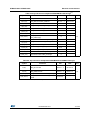
Device summary . . . . . . . . . . . . . . . . . . . . . . . . . . . . . . . . . . . . . . . . . . . . . . . . . . . . . . . . . . 1
STM32F745xx and STM32F746xx features and peripheral counts . . . . . . . . . . . . . . . . . . 13
Voltage regulator configuration mode versus device operating mode . . . . . . . . . . . . . . . . 27
Regulator ON/OFF and internal reset ON/OFF availability. . . . . . . . . . . . . . . . . . . . . . . . . 30
Voltage regulator modes in Stop mode . . . . . . . . . . . . . . . . . . . . . . . . . . . . . . . . . . . . . . . 31
Timer feature comparison . . . . . . . . . . . . . . . . . . . . . . . . . . . . . . . . . . . . . . . . . . . . . . . . . . 33
I2C implementation . . . . . . . . . . . . . . . . . . . . . . . . . . . . . . . . . . . . . . . . . . . . . . . . . . . . . . . 36
USART implementation . . . . . . . . . . . . . . . . . . . . . . . . . . . . . . . . . . . . . . . . . . . . . . . . . . . 37
Legend/abbreviations used in the pinout table . . . . . . . . . . . . . . . . . . . . . . . . . . . . . . . . . . 52
STM32F745xx and STM32F746xx pin and ball definition . . . . . . . . . . . . . . . . . . . . . . . . . 52
FMC pin definition . . . . . . . . . . . . . . . . . . . . . . . . . . . . . . . . . . . . . . . . . . . . . . . . . . . . . . . . 72
STM32F745xx and STM32F746xx alternate function mapping . . . . . . . . . . . . . . . . . . . . . 75
STM32F745xx and STM32F746xx register boundary addresses. . . . . . . . . . . . . . . . . . . . 89
STM32F745xx and STM32F746xx register boundary addresses. . . . . . . . . . . . . . . . . . . . 93
Voltage characteristics . . . . . . . . . . . . . . . . . . . . . . . . . . . . . . . . . . . . . . . . . . . . . . . . . . . . 99
Current characteristics . . . . . . . . . . . . . . . . . . . . . . . . . . . . . . . . . . . . . . . . . . . . . . . . . . . 100
Thermal characteristics. . . . . . . . . . . . . . . . . . . . . . . . . . . . . . . . . . . . . . . . . . . . . . . . . . . 100
General operating conditions . . . . . . . . . . . . . . . . . . . . . . . . . . . . . . . . . . . . . . . . . . . . . . 101
Limitations depending on the operating power supply range . . . . . . . . . . . . . . . . . . . . . . 103
VCAP1/VCAP2 operating conditions . . . . . . . . . . . . . . . . . . . . . . . . . . . . . . . . . . . . . . . . 104
Operating conditions at power-up / power-down (regulator ON) . . . . . . . . . . . . . . . . . . . 104
Operating conditions at power-up / power-down (regulator OFF). . . . . . . . . . . . . . . . . . . 104
reset and power control block characteristics . . . . . . . . . . . . . . . . . . . . . . . . . . . . . . . . . 105
Over-drive switching characteristics . . . . . . . . . . . . . . . . . . . . . . . . . . . . . . . . . . . . . . . . . 106
Typical and maximum current consumption in Run mode, code with data processing
running from ITCM RAM, regulator ON . . . . . . . . . . . . . . . . . . . . . . . . . . . . . . . . . . . . . . 107
Typical and maximum current consumption in Run mode, code with data processing
running from Flash memory (ART ON except prefetch / L1-cache ON)
or SRAM on AXI (L1-cache ON), regulator ON . . . . . . . . . . . . . . . . . . . . . . . . . . . . . . . . 108
Typical and maximum current consumption in Run mode, code with data processing
running from Flash memory or SRAM on AXI (L1-cache disabled), regulator ON . . . . . 109
Typical and maximum current consumption in Run mode, code with data processing
running from Flash memory on ITCM interface (ART disabled), regulator ON . . . . . . . . 110
Typical and maximum current consumption in Run mode, code with data processing
running from Flash memory (ART ON except prefetch / L1-cache ON)
or SRAM on AXI (L1-cache ON), regulator OFF. . . . . . . . . . . . . . . . . . . . . . . . . . . . . . . . 111
Typical and maximum current consumption in Sleep mode, regulator ON. . . . . . . . . . . . 112
Typical and maximum current consumption in Sleep mode, regulator OFF . . . . . . . . . . . 112
Typical and maximum current consumptions in Stop mode . . . . . . . . . . . . . . . . . . . . . . . 113
Typical and maximum current consumptions in Standby mode . . . . . . . . . . . . . . . . . . . . 114
Typical and maximum current consumptions in VBAT mode. . . . . . . . . . . . . . . . . . . . . . . 115
Switching output I/O current consumption . . . . . . . . . . . . . . . . . . . . . . . . . . . . . . . . . . . . 119
Peripheral current consumption . . . . . . . . . . . . . . . . . . . . . . . . . . . . . . . . . . . . . . . . . . . . 121
Low-power mode wakeup timings . . . . . . . . . . . . . . . . . . . . . . . . . . . . . . . . . . . . . . . . . . 124
High-speed external user clock characteristics. . . . . . . . . . . . . . . . . . . . . . . . . . . . . . . . . 125
Low-speed external user clock characteristics . . . . . . . . . . . . . . . . . . . . . . . . . . . . . . . . . 126
HSE 4-26 MHz oscillator characteristics. . . . . . . . . . . . . . . . . . . . . . . . . . . . . . . . . . . . . . 127
LSE oscillator characteristics (fLSE = 32.768 kHz) . . . . . . . . . . . . . . . . . . . . . . . . . . . . . . 128
DocID027590 Rev 1
STM32F745xx STM32F746xx
Table 42.
Table 43.
Table 44.
Table 45.
Table 46.
Table 47.
Table 48.
Table 49.
Table 50.
Table 51.
Table 52.
Table 53.
Table 54.
Table 55.
Table 56.
Table 57.
Table 58.
Table 59.
Table 60.
Table 61.
Table 62.
Table 63.
Table 64.
Table 65.
Table 66.
Table 67.
Table 68.
Table 69.
Table 70.
Table 71.
Table 72.
Table 73.
Table 74.
Table 75.
Table 76.
Table 77.
Table 78.
Table 79.
Table 80.
Table 81.
Table 82.
Table 83.
Table 84.
Table 85.
Table 86.
Table 87.
Table 88.
Table 89.
Table 90.
Table 91.
Table 92.
Table 93.
List of tables
HSI oscillator characteristics . . . . . . . . . . . . . . . . . . . . . . . . . . . . . . . . . . . . . . . . . . . . . . 130
LSI oscillator characteristics . . . . . . . . . . . . . . . . . . . . . . . . . . . . . . . . . . . . . . . . . . . . . . 131
Main PLL characteristics. . . . . . . . . . . . . . . . . . . . . . . . . . . . . . . . . . . . . . . . . . . . . . . . . . 131
PLLI2S characteristics . . . . . . . . . . . . . . . . . . . . . . . . . . . . . . . . . . . . . . . . . . . . . . . . . . . 132
PLLISAI characteristics. . . . . . . . . . . . . . . . . . . . . . . . . . . . . . . . . . . . . . . . . . . . . . . . . . . 133
SSCG parameters constraint . . . . . . . . . . . . . . . . . . . . . . . . . . . . . . . . . . . . . . . . . . . . . . 134
Flash memory characteristics . . . . . . . . . . . . . . . . . . . . . . . . . . . . . . . . . . . . . . . . . . . . . . 136
Flash memory programming . . . . . . . . . . . . . . . . . . . . . . . . . . . . . . . . . . . . . . . . . . . . . . . 136
Flash memory programming with VPP . . . . . . . . . . . . . . . . . . . . . . . . . . . . . . . . . . . . . . . 137
Flash memory endurance and data retention . . . . . . . . . . . . . . . . . . . . . . . . . . . . . . . . . . 138
EMS characteristics . . . . . . . . . . . . . . . . . . . . . . . . . . . . . . . . . . . . . . . . . . . . . . . . . . . . . 138
EMI characteristics . . . . . . . . . . . . . . . . . . . . . . . . . . . . . . . . . . . . . . . . . . . . . . . . . . . . . . 139
ESD absolute maximum ratings . . . . . . . . . . . . . . . . . . . . . . . . . . . . . . . . . . . . . . . . . . . . 140
Electrical sensitivities . . . . . . . . . . . . . . . . . . . . . . . . . . . . . . . . . . . . . . . . . . . . . . . . . . . . 140
I/O current injection susceptibility . . . . . . . . . . . . . . . . . . . . . . . . . . . . . . . . . . . . . . . . . . . 141
I/O static characteristics . . . . . . . . . . . . . . . . . . . . . . . . . . . . . . . . . . . . . . . . . . . . . . . . . . 141
Output voltage characteristics . . . . . . . . . . . . . . . . . . . . . . . . . . . . . . . . . . . . . . . . . . . . . 144
I/O AC characteristics . . . . . . . . . . . . . . . . . . . . . . . . . . . . . . . . . . . . . . . . . . . . . . . . . . . . 145
NRST pin characteristics . . . . . . . . . . . . . . . . . . . . . . . . . . . . . . . . . . . . . . . . . . . . . . . . . 147
TIMx characteristics . . . . . . . . . . . . . . . . . . . . . . . . . . . . . . . . . . . . . . . . . . . . . . . . . . . . . 148
RTC characteristics . . . . . . . . . . . . . . . . . . . . . . . . . . . . . . . . . . . . . . . . . . . . . . . . . . . . . 148
ADC characteristics . . . . . . . . . . . . . . . . . . . . . . . . . . . . . . . . . . . . . . . . . . . . . . . . . . . . . 148
ADC static accuracy at fADC = 18 MHz . . . . . . . . . . . . . . . . . . . . . . . . . . . . . . . . . . . . . . . 150
ADC static accuracy at fADC = 30 MHz . . . . . . . . . . . . . . . . . . . . . . . . . . . . . . . . . . . . . . . 150
ADC static accuracy at fADC = 36 MHz . . . . . . . . . . . . . . . . . . . . . . . . . . . . . . . . . . . . . . . 151
ADC dynamic accuracy at fADC = 18 MHz - limited test conditions . . . . . . . . . . . . . . . . . 151
ADC dynamic accuracy at fADC = 36 MHz - limited test conditions . . . . . . . . . . . . . . . . . 151
Temperature sensor characteristics . . . . . . . . . . . . . . . . . . . . . . . . . . . . . . . . . . . . . . . . . 154
Temperature sensor calibration values. . . . . . . . . . . . . . . . . . . . . . . . . . . . . . . . . . . . . . . 154
VBAT monitoring characteristics . . . . . . . . . . . . . . . . . . . . . . . . . . . . . . . . . . . . . . . . . . . . 154
internal reference voltage . . . . . . . . . . . . . . . . . . . . . . . . . . . . . . . . . . . . . . . . . . . . . . . . 154
Internal reference voltage calibration values . . . . . . . . . . . . . . . . . . . . . . . . . . . . . . . . . . 155
DAC characteristics . . . . . . . . . . . . . . . . . . . . . . . . . . . . . . . . . . . . . . . . . . . . . . . . . . . . . 155
Minimum I2CCLK frequency in all I2C modes . . . . . . . . . . . . . . . . . . . . . . . . . . . . . . . . . 157
I2C analog filter characteristics. . . . . . . . . . . . . . . . . . . . . . . . . . . . . . . . . . . . . . . . . . . . . 158
SPI dynamic characteristics . . . . . . . . . . . . . . . . . . . . . . . . . . . . . . . . . . . . . . . . . . . . . . . 159
I2S dynamic characteristics . . . . . . . . . . . . . . . . . . . . . . . . . . . . . . . . . . . . . . . . . . . . . . . 162
SAI characteristics . . . . . . . . . . . . . . . . . . . . . . . . . . . . . . . . . . . . . . . . . . . . . . . . . . . . . . 164
USB OTG full speed startup time . . . . . . . . . . . . . . . . . . . . . . . . . . . . . . . . . . . . . . . . . . . 166
USB OTG full speed DC electrical characteristics . . . . . . . . . . . . . . . . . . . . . . . . . . . . . . 166
USB OTG full speed electrical characteristics . . . . . . . . . . . . . . . . . . . . . . . . . . . . . . . . . 167
USB HS DC electrical characteristics . . . . . . . . . . . . . . . . . . . . . . . . . . . . . . . . . . . . . . . . 167
USB HS clock timing parameters . . . . . . . . . . . . . . . . . . . . . . . . . . . . . . . . . . . . . . . . . . . 168
Dynamic characteristics: USB ULPI . . . . . . . . . . . . . . . . . . . . . . . . . . . . . . . . . . . . . . . . . 169
Ethernet DC electrical characteristics . . . . . . . . . . . . . . . . . . . . . . . . . . . . . . . . . . . . . . . . 169
Dynamics characteristics: Ethernet MAC signals for SMI. . . . . . . . . . . . . . . . . . . . . . . . . 170
Dynamics characteristics: Ethernet MAC signals for RMII . . . . . . . . . . . . . . . . . . . . . . . . 171
Dynamics characteristics: Ethernet MAC signals for MII . . . . . . . . . . . . . . . . . . . . . . . . . 171
Asynchronous non-multiplexed SRAM/PSRAM/NOR read timings . . . . . . . . . . . . . . . . . 174
Asynchronous non-multiplexed SRAM/PSRAM/NOR read - NWAIT timings . . . . . . . . . . 174
Asynchronous non-multiplexed SRAM/PSRAM/NOR write timings . . . . . . . . . . . . . . . . . 175
Asynchronous non-multiplexed SRAM/PSRAM/NOR write - NWAIT timings. . . . . . . . . . 176
DocID027590 Rev 1
7/226
8
List of tables
Table 94.
Table 95.
Table 96.
Table 97.
Table 98.
Table 99.
Table 100.
Table 101.
Table 102.
Table 103.
Table 104.
Table 105.
Table 106.
Table 107.
Table 108.
Table 109.
Table 110.
Table 111.
Table 112.
Table 113.
Table 114.
Table 115.
Table 116.
Table 117.
Table 118.
Table 119.
Table 120.
Table 121.
Table 122.
Table 123.
Table 124.
Table 125.
Table 126.
Table 127.
8/226
STM32F745xx STM32F746xx
Asynchronous multiplexed PSRAM/NOR read timings. . . . . . . . . . . . . . . . . . . . . . . . . . . 177
Asynchronous multiplexed PSRAM/NOR read-NWAIT timings . . . . . . . . . . . . . . . . . . . . 177
Asynchronous multiplexed PSRAM/NOR write timings . . . . . . . . . . . . . . . . . . . . . . . . . . 178
Asynchronous multiplexed PSRAM/NOR write-NWAIT timings . . . . . . . . . . . . . . . . . . . . 179
Synchronous multiplexed NOR/PSRAM read timings . . . . . . . . . . . . . . . . . . . . . . . . . . . 181
Synchronous multiplexed PSRAM write timings . . . . . . . . . . . . . . . . . . . . . . . . . . . . . . . . 183
Synchronous non-multiplexed NOR/PSRAM read timings . . . . . . . . . . . . . . . . . . . . . . . . 184
Synchronous non-multiplexed PSRAM write timings . . . . . . . . . . . . . . . . . . . . . . . . . . . . 186
Switching characteristics for NAND Flash read cycles . . . . . . . . . . . . . . . . . . . . . . . . . . . 188
Switching characteristics for NAND Flash write cycles. . . . . . . . . . . . . . . . . . . . . . . . . . . 189
SDRAM read timings . . . . . . . . . . . . . . . . . . . . . . . . . . . . . . . . . . . . . . . . . . . . . . . . . . . . 190
LPSDR SDRAM read timings . . . . . . . . . . . . . . . . . . . . . . . . . . . . . . . . . . . . . . . . . . . . . . 190
SDRAM write timings . . . . . . . . . . . . . . . . . . . . . . . . . . . . . . . . . . . . . . . . . . . . . . . . . . . . 191
LPSDR SDRAM write timings . . . . . . . . . . . . . . . . . . . . . . . . . . . . . . . . . . . . . . . . . . . . . . 192
Quad SPI characteristics in SDR mode . . . . . . . . . . . . . . . . . . . . . . . . . . . . . . . . . . . . . . 192
Quad SPI characteristics in DDR mode . . . . . . . . . . . . . . . . . . . . . . . . . . . . . . . . . . . . . . 193
DCMI characteristics. . . . . . . . . . . . . . . . . . . . . . . . . . . . . . . . . . . . . . . . . . . . . . . . . . . . . 194
LTDC characteristics . . . . . . . . . . . . . . . . . . . . . . . . . . . . . . . . . . . . . . . . . . . . . . . . . . . . 195
Dynamic characteristics: SD / MMC characteristics, VDD=2.7V to 3.6V . . . . . . . . . . . . . 198
Dynamic characteristics: eMMC characteristics, VDD=1.71V to 1.9V . . . . . . . . . . . . . . . 198
LQPF100, 14 x 14 mm 100-pin low-profile quad flat package mechanical data. . . . . . . . 200
WLCSP143 - 143-ball, 4.539x 5.849 mm, 0.4 mm pitch wafer level chip scale
package mechanical data . . . . . . . . . . . . . . . . . . . . . . . . . . . . . . . . . . . . . . . . . . . . . . . . 202
WLCSP143 recommended PCB design rules . . . . . . . . . . . . . . . . . . . . . . . . . . . . . . . . . 204
LQFP144, 20 x 20 mm, 144-pin low-profile quad flat package
mechanical data . . . . . . . . . . . . . . . . . . . . . . . . . . . . . . . . . . . . . . . . . . . . . . . . . . . . . . . . 205
LQFP176, 24 x 24 mm, 176-pin low-profile quad flat package
mechanical data . . . . . . . . . . . . . . . . . . . . . . . . . . . . . . . . . . . . . . . . . . . . . . . . . . . . . . . . 208
LQFP208, 28 x 28 mm, 208-pin low-profile quad flat package
mechanical data . . . . . . . . . . . . . . . . . . . . . . . . . . . . . . . . . . . . . . . . . . . . . . . . . . . . . . . . 212
UFBGA176+25, 10 × 10 × 0.65 mm ultra thin fine-pitch ball grid array
package mechanical data . . . . . . . . . . . . . . . . . . . . . . . . . . . . . . . . . . . . . . . . . . . . . . . . . 216
UFBGA176+25 recommended PCB design rules (0.65 mm pitch BGA) . . . . . . . . . . . . . 217
TFBGA216, 13 × 13 × 0.8mm thin fine-pitch ball grid array
package mechanical data . . . . . . . . . . . . . . . . . . . . . . . . . . . . . . . . . . . . . . . . . . . . . . . . . 219
TFBGA216 recommended PCB design rules (0.8 mm pitch BGA). . . . . . . . . . . . . . . . . . 220
Package thermal characteristics . . . . . . . . . . . . . . . . . . . . . . . . . . . . . . . . . . . . . . . . . . . . 222
Ordering information scheme . . . . . . . . . . . . . . . . . . . . . . . . . . . . . . . . . . . . . . . . . . . . . . 223
Limitations depending on the operating power supply range . . . . . . . . . . . . . . . . . . . . . . 224
Document revision history . . . . . . . . . . . . . . . . . . . . . . . . . . . . . . . . . . . . . . . . . . . . . . . . 225
DocID027590 Rev 1
STM32F745xx STM32F746xx
List of figures
List of figures
Figure 1.
Figure 2.
Figure 3.
Figure 4.
Figure 5.
Figure 6.
Figure 7.
Figure 8.
Figure 9.
Figure 10.
Figure 11.
Figure 12.
Figure 13.
Figure 14.
Figure 15.
Figure 16.
Figure 17.
Figure 18.
Figure 19.
Figure 20.
Figure 21.
Figure 22.
Figure 23.
Figure 24.
Figure 25.
Figure 26.
Figure 27.
Figure 28.
Figure 29.
Figure 30.
Figure 31.
Figure 32.
Figure 33.
Figure 34.
Figure 35.
Figure 36.
Figure 37.
Figure 38.
Figure 39.
Figure 40.
Figure 41.
Compatible board design for LQFP100 package . . . . . . . . . . . . . . . . . . . . . . . . . . . . . . . . 15
STM32F745xx and STM32F746xx block diagram . . . . . . . . . . . . . . . . . . . . . . . . . . . . . . . 16
STM32F745xx and STM32F746xx AXI-AHB bus matrix architecture . . . . . . . . . . . . . . . . 19
VDDUSB connected to VDD power supply . . . . . . . . . . . . . . . . . . . . . . . . . . . . . . . . . . . . 24
VDDUSB connected to external power supply . . . . . . . . . . . . . . . . . . . . . . . . . . . . . . . . . . 24
Power supply supervisor interconnection with internal reset OFF . . . . . . . . . . . . . . . . . . . 25
PDR_ON control with internal reset OFF . . . . . . . . . . . . . . . . . . . . . . . . . . . . . . . . . . . . . . 26
Regulator OFF . . . . . . . . . . . . . . . . . . . . . . . . . . . . . . . . . . . . . . . . . . . . . . . . . . . . . . . . . . 28
Startup in regulator OFF: slow VDD slope
- power-down reset risen after VCAP_1/VCAP_2 stabilization . . . . . . . . . . . . . . . . . . . . . . . . 29
Startup in regulator OFF mode: fast VDD slope
- power-down reset risen before VCAP_1/VCAP_2 stabilization . . . . . . . . . . . . . . . . . . . . . . 29
STM32F74xVx LQFP100 pinout . . . . . . . . . . . . . . . . . . . . . . . . . . . . . . . . . . . . . . . . . . . . . 45
STM32F74xZx WLCSP143 ballout . . . . . . . . . . . . . . . . . . . . . . . . . . . . . . . . . . . . . . . . . . . 46
STM32F74xZx LQFP144 pinout . . . . . . . . . . . . . . . . . . . . . . . . . . . . . . . . . . . . . . . . . . . . . 47
STM32F74xIx LQFP176 pinout . . . . . . . . . . . . . . . . . . . . . . . . . . . . . . . . . . . . . . . . . . . . . 48
STM32F74xBx LQFP208 pinout . . . . . . . . . . . . . . . . . . . . . . . . . . . . . . . . . . . . . . . . . . . . . 49
STM32F74xIx UFBGA176 ballout . . . . . . . . . . . . . . . . . . . . . . . . . . . . . . . . . . . . . . . . . . . 50
STM32F74xNx TFBGA216 ballout . . . . . . . . . . . . . . . . . . . . . . . . . . . . . . . . . . . . . . . . . . . 51
Memory map . . . . . . . . . . . . . . . . . . . . . . . . . . . . . . . . . . . . . . . . . . . . . . . . . . . . . . . . . . . . 88
Pin loading conditions . . . . . . . . . . . . . . . . . . . . . . . . . . . . . . . . . . . . . . . . . . . . . . . . . . . . . 97
Pin input voltage . . . . . . . . . . . . . . . . . . . . . . . . . . . . . . . . . . . . . . . . . . . . . . . . . . . . . . . . . 97
Power supply scheme. . . . . . . . . . . . . . . . . . . . . . . . . . . . . . . . . . . . . . . . . . . . . . . . . . . . . 98
Current consumption measurement scheme . . . . . . . . . . . . . . . . . . . . . . . . . . . . . . . . . . . 99
External capacitor CEXT . . . . . . . . . . . . . . . . . . . . . . . . . . . . . . . . . . . . . . . . . . . . . . . . . . 103
Typical VBAT current consumption (RTC ON/BKP SRAM OFF and
LSE in low drive mode) . . . . . . . . . . . . . . . . . . . . . . . . . . . . . . . . . . . . . . . . . . . . . . . . . . . 116
Typical VBAT current consumption (RTC ON/BKP SRAM OFF and
LSE in medium low drive mode) . . . . . . . . . . . . . . . . . . . . . . . . . . . . . . . . . . . . . . . . . . . . 116
Typical VBAT current consumption (RTC ON/BKP SRAM OFF and
LSE in medium high drive mode) . . . . . . . . . . . . . . . . . . . . . . . . . . . . . . . . . . . . . . . . . . . 117
Typical VBAT current consumption (RTC ON/BKP SRAM OFF and
LSE in high drive mode) . . . . . . . . . . . . . . . . . . . . . . . . . . . . . . . . . . . . . . . . . . . . . . . . . . 117
Typical VBAT current consumption (RTC ON/BKP SRAM OFF and
LSE in high medium drive mode) . . . . . . . . . . . . . . . . . . . . . . . . . . . . . . . . . . . . . . . . . . . 118
High-speed external clock source AC timing diagram . . . . . . . . . . . . . . . . . . . . . . . . . . . 126
Low-speed external clock source AC timing diagram . . . . . . . . . . . . . . . . . . . . . . . . . . . . 127
Typical application with an 8 MHz crystal . . . . . . . . . . . . . . . . . . . . . . . . . . . . . . . . . . . . . 128
Typical application with a 32.768 kHz crystal . . . . . . . . . . . . . . . . . . . . . . . . . . . . . . . . . . 129
HSI deviation versus temperature . . . . . . . . . . . . . . . . . . . . . . . . . . . . . . . . . . . . . . . . . . 130
LSI deviation versus temperature . . . . . . . . . . . . . . . . . . . . . . . . . . . . . . . . . . . . . . . . . . . 131
PLL output clock waveforms in center spread mode . . . . . . . . . . . . . . . . . . . . . . . . . . . . 135
PLL output clock waveforms in down spread mode . . . . . . . . . . . . . . . . . . . . . . . . . . . . . 136
FT I/O input characteristics . . . . . . . . . . . . . . . . . . . . . . . . . . . . . . . . . . . . . . . . . . . . . . . . 143
I/O AC characteristics definition . . . . . . . . . . . . . . . . . . . . . . . . . . . . . . . . . . . . . . . . . . . . 146
Recommended NRST pin protection . . . . . . . . . . . . . . . . . . . . . . . . . . . . . . . . . . . . . . . . 147
ADC accuracy characteristics . . . . . . . . . . . . . . . . . . . . . . . . . . . . . . . . . . . . . . . . . . . . . . 152
Typical connection diagram using the ADC . . . . . . . . . . . . . . . . . . . . . . . . . . . . . . . . . . . 152
DocID027590 Rev 1
9/226
11
List of figures
Figure 42.
Figure 43.
Figure 44.
Figure 45.
Figure 46.
Figure 47.
Figure 48.
Figure 49.
Figure 50.
Figure 51.
Figure 52.
Figure 53.
Figure 54.
Figure 55.
Figure 56.
Figure 57.
Figure 58.
Figure 59.
Figure 60.
Figure 61.
Figure 62.
Figure 63.
Figure 64.
Figure 65.
Figure 66.
Figure 67.
Figure 68.
Figure 69.
Figure 70.
Figure 71.
Figure 72.
Figure 73.
Figure 74.
Figure 75.
Figure 76.
Figure 77.
Figure 78.
Figure 79.
Figure 80.
Figure 81.
Figure 82.
Figure 83.
Figure 84.
Figure 85.
Figure 86.
10/226
STM32F745xx STM32F746xx
Power supply and reference decoupling (VREF+ not connected to VDDA). . . . . . . . . . . . . 153
Power supply and reference decoupling (VREF+ connected to VDDA). . . . . . . . . . . . . . . . 153
12-bit buffered /non-buffered DAC . . . . . . . . . . . . . . . . . . . . . . . . . . . . . . . . . . . . . . . . . . 157
SPI timing diagram - slave mode and CPHA = 0 . . . . . . . . . . . . . . . . . . . . . . . . . . . . . . . 160
SPI timing diagram - slave mode and CPHA = 1(1) . . . . . . . . . . . . . . . . . . . . . . . . . . . . . 161
SPI timing diagram - master mode(1) . . . . . . . . . . . . . . . . . . . . . . . . . . . . . . . . . . . . . . . . 161
I2S slave timing diagram (Philips protocol)(1) . . . . . . . . . . . . . . . . . . . . . . . . . . . . . . . . . . 163
I2S master timing diagram (Philips protocol)(1) . . . . . . . . . . . . . . . . . . . . . . . . . . . . . . . . . 163
SAI master timing waveforms . . . . . . . . . . . . . . . . . . . . . . . . . . . . . . . . . . . . . . . . . . . . . . 165
SAI slave timing waveforms . . . . . . . . . . . . . . . . . . . . . . . . . . . . . . . . . . . . . . . . . . . . . . . 165
USB OTG full speed timings: definition of data signal rise and fall time . . . . . . . . . . . . . . 167
ULPI timing diagram . . . . . . . . . . . . . . . . . . . . . . . . . . . . . . . . . . . . . . . . . . . . . . . . . . . . . 168
Ethernet SMI timing diagram . . . . . . . . . . . . . . . . . . . . . . . . . . . . . . . . . . . . . . . . . . . . . . 170
Ethernet RMII timing diagram . . . . . . . . . . . . . . . . . . . . . . . . . . . . . . . . . . . . . . . . . . . . . . 170
Ethernet MII timing diagram . . . . . . . . . . . . . . . . . . . . . . . . . . . . . . . . . . . . . . . . . . . . . . . 171
Asynchronous non-multiplexed SRAM/PSRAM/NOR read waveforms . . . . . . . . . . . . . . 173
Asynchronous non-multiplexed SRAM/PSRAM/NOR write waveforms . . . . . . . . . . . . . . 175
Asynchronous multiplexed PSRAM/NOR read waveforms. . . . . . . . . . . . . . . . . . . . . . . . 176
Asynchronous multiplexed PSRAM/NOR write waveforms . . . . . . . . . . . . . . . . . . . . . . . 178
Synchronous multiplexed NOR/PSRAM read timings . . . . . . . . . . . . . . . . . . . . . . . . . . . 180
Synchronous multiplexed PSRAM write timings . . . . . . . . . . . . . . . . . . . . . . . . . . . . . . . . 182
Synchronous non-multiplexed NOR/PSRAM read timings . . . . . . . . . . . . . . . . . . . . . . . . 184
Synchronous non-multiplexed PSRAM write timings . . . . . . . . . . . . . . . . . . . . . . . . . . . . 185
NAND controller waveforms for read access . . . . . . . . . . . . . . . . . . . . . . . . . . . . . . . . . . 187
NAND controller waveforms for write access . . . . . . . . . . . . . . . . . . . . . . . . . . . . . . . . . . 187
NAND controller waveforms for common memory read access . . . . . . . . . . . . . . . . . . . . 188
NAND controller waveforms for common memory write access. . . . . . . . . . . . . . . . . . . . 188
SDRAM read access waveforms (CL = 1) . . . . . . . . . . . . . . . . . . . . . . . . . . . . . . . . . . . . 189
SDRAM write access waveforms . . . . . . . . . . . . . . . . . . . . . . . . . . . . . . . . . . . . . . . . . . . 191
Quad SPI timing diagram - SDR mode . . . . . . . . . . . . . . . . . . . . . . . . . . . . . . . . . . . . . . . 194
Quad SPI timing diagram - DDR mode. . . . . . . . . . . . . . . . . . . . . . . . . . . . . . . . . . . . . . . 194
DCMI timing diagram . . . . . . . . . . . . . . . . . . . . . . . . . . . . . . . . . . . . . . . . . . . . . . . . . . . . 195
LCD-TFT horizontal timing diagram . . . . . . . . . . . . . . . . . . . . . . . . . . . . . . . . . . . . . . . . . 196
LCD-TFT vertical timing diagram . . . . . . . . . . . . . . . . . . . . . . . . . . . . . . . . . . . . . . . . . . . 196
SDIO high-speed mode . . . . . . . . . . . . . . . . . . . . . . . . . . . . . . . . . . . . . . . . . . . . . . . . . . 197
SD default mode . . . . . . . . . . . . . . . . . . . . . . . . . . . . . . . . . . . . . . . . . . . . . . . . . . . . . . . . 197
LQFP100, 14 x 14 mm 100-pin low-profile quad flat package outline . . . . . . . . . . . . . . . 199
LQFP100, 14 x 14 mm, 100-pin low-profile quad flat package
recommended footprint . . . . . . . . . . . . . . . . . . . . . . . . . . . . . . . . . . . . . . . . . . . . . . . . . . . 201
LQFP100, 14 x 14 mm, 100-pin low-profile quad flat package
top view example . . . . . . . . . . . . . . . . . . . . . . . . . . . . . . . . . . . . . . . . . . . . . . . . . . . . . . . 201
WLCSP143 - 143-ball, 4.539x 5.849 mm, 0.4 mm pitch wafer level chip scale
package outline . . . . . . . . . . . . . . . . . . . . . . . . . . . . . . . . . . . . . . . . . . . . . . . . . . . . . . . . 202
WLCSP143 - 143-ball, 4.539x 5.849 mm, 0.4 mm pitch wafer level chip scale
package recommended footprint . . . . . . . . . . . . . . . . . . . . . . . . . . . . . . . . . . . . . . . . . . . 203
WLCSP143, 0.4 mm pitch wafer level chip scale package
top view example . . . . . . . . . . . . . . . . . . . . . . . . . . . . . . . . . . . . . . . . . . . . . . . . . . . . . . . 204
LQFP144, 20 x 20 mm, 144-pin low-profile quad flat package outline . . . . . . . . . . . . . . . 205
LQFP144, 20 x 20 mm, 144-pin low-profile quad flat package
recommended footprint . . . . . . . . . . . . . . . . . . . . . . . . . . . . . . . . . . . . . . . . . . . . . . . . . . . 206
LQFP144, 20 x 20mm, 144-pin low-profile quad flat package
top view example . . . . . . . . . . . . . . . . . . . . . . . . . . . . . . . . . . . . . . . . . . . . . . . . . . . . . . 207
DocID027590 Rev 1
STM32F745xx STM32F746xx
Figure 87.
Figure 88.
Figure 89.
Figure 90.
Figure 91.
Figure 92.
Figure 93.
Figure 94.
Figure 95.
Figure 96.
Figure 97.
Figure 98.
List of figures
LQFP176, 24 x 24 mm, 176-pin low-profile quad flat package outline . . . . . . . . . . . . . . . 208
LQFP176, 24 x 24 mm, 176-pin low-profile quad flat package
recommended footprint . . . . . . . . . . . . . . . . . . . . . . . . . . . . . . . . . . . . . . . . . . . . . . . . . . . 210
LQFP176, 24 x 24 mm, 176-pin low-profile quad flat package
top view example . . . . . . . . . . . . . . . . . . . . . . . . . . . . . . . . . . . . . . . . . . . . . . . . . . . . . . . 211
LQFP208, 28 x 28 mm, 208-pin low-profile quad flat package outline . . . . . . . . . . . . . . . 212
LQFP208, 28 x 28 mm, 208-pin low-profile quad flat package
recommended footprint . . . . . . . . . . . . . . . . . . . . . . . . . . . . . . . . . . . . . . . . . . . . . . . . . . . 214
LQFP208, 28 x 28 mm, 208-pin low-profile quad flat package
top view example . . . . . . . . . . . . . . . . . . . . . . . . . . . . . . . . . . . . . . . . . . . . . . . . . . . . . . . 215
UFBGA176+25, 10 × 10 × 0.65 mm ultra thin fine-pitch ball grid array
package outline. . . . . . . . . . . . . . . . . . . . . . . . . . . . . . . . . . . . . . . . . . . . . . . . . . . . . . . . . 216
UFBGA176+25, 10 x 10 mm x 0.65 mm, ultra fine-pitch ball grid array
package recommended footprint . . . . . . . . . . . . . . . . . . . . . . . . . . . . . . . . . . . . . . . . . . . 217
UFBGA176+25, 10 × 10 × 0.6 mm ultra thin fine-pitch ball grid array
package top view example . . . . . . . . . . . . . . . . . . . . . . . . . . . . . . . . . . . . . . . . . . . . . . . . 218
TFBGA216, 13 × 13 × 0.8mm thin fine-pitch ball grid array
package outline. . . . . . . . . . . . . . . . . . . . . . . . . . . . . . . . . . . . . . . . . . . . . . . . . . . . . . . . . 219
TFBGA216, 13 x 13 mm, 0.8 mm pitch, thin fine-pitch ball grid array
package recommended footprint . . . . . . . . . . . . . . . . . . . . . . . . . . . . . . . . . . . . . . . . . . . 220
TFBGA216, 13 × 13 × 0.8mm thin fine-pitch ball grid array
package top view example . . . . . . . . . . . . . . . . . . . . . . . . . . . . . . . . . . . . . . . . . . . . . . . . 221
DocID027590 Rev 1
11/226
11
Description
1
STM32F745xx STM32F746xx
Description
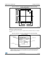
The STM32F745xx and STM32F746xx devices are based on the high-performance ARM®
Cortex®-M7 32-bit RISC core operating at up to 216 MHz frequency. The Cortex®-M7 core
features a single floating point unit (SFPU) precision which supports all ARM® singleprecision data-processing instructions and data types. It also implements a full set of DSP
instructions and a memory protection unit (MPU) which enhances the application security.
The STM32F745xx and STM32F746xx devices incorporate high-speed embedded
memories with Flash memory up to 1 Mbyte, 320 KB of SRAM (including 64 KB of Data
TCM RAM for critical real time data), 16 KB of instruction TCM RAM (for critical real time
routines), 4 KB of backup SRAM available in the lowest power modes, and an extensive
range of enhanced I/Os and peripherals connected to two APB buses, two AHB buses, a
32-bit multi-AHB bus matrix and a multi layer AXI interconnect supporting internal and
external memories access.
All devices offer three 12-bit ADCs, two DACs, a low-power RTC, thirteen general-purpose
16-bit timers including two PWM timers for motor control and one low-power timer available
in Stop mode, two general-purpose 32-bit timers, a true random number generator (RNG).
They also feature standard and advanced communication interfaces.
•
•
•
•
•
•
•
•
•
•
•
•
Up to four I2Cs
Six SPIs, three I2Ss in duplex mode. To achieve the audio class accuracy, the I2S
peripherals can be clocked via a dedicated internal audio PLL or via an external clock
to allow synchronization.
Four USARTs plus four UARTs
An USB OTG full-speed and a USB OTG high-speed with full-speed capability (with the
ULPI),
Two CANs
Two SAI serial audio interfaces
An SDMMC host interface
Ethernet and camera interfaces
LCD-TFT display controller
Chrom-ART Accelerator™
SPDIFRX interface
HDMI-CEC
Advanced peripherals include an SDMMC interface, a flexible memory control (FMC)
interface, a Quad SPI Flash memory interface, a camera interface for CMOS sensors. Refer
to Table 2: STM32F745xx and STM32F746xx features and peripheral counts for the list of
peripherals available on each part number.
The STM32F745xx and STM32F746xx devices operate in the –40 to +105 °C temperature
range from a 1.7 to 3.6 V power supply. A dedicated supply input for USB (OTG_FS and
OTG_HS) is available on all the packages except LQFP100 for a greater power supply
choice.
The supply voltage can drop to 1.7 V with the use of an external power supply supervisor
(refer to Section 2.17.2: Internal reset OFF). A comprehensive set of power-saving mode
allows the design of low-power applications.
The STM32F745xx and STM32F746xx devices offer devices in 7 packages ranging from
100 pins to 216 pins. The set of included peripherals changes with the device chosen.
12/226
DocID027590 Rev 1
•
Motor drive and application control,
•
Medical equipment,
•
Industrial applications: PLC, inverters, circuit breakers,
•
Printers, and scanners,
•
Alarm systems, video intercom, and HVAC,
•
Home audio appliances,
•
Mobile applications, Internet of Things,
•
Wearable devices: smartwatches.
STM32F745xx STM32F746xx
These features make the STM32F745xx and STM32F746xx microcontrollers suitable for a wide range of applications:
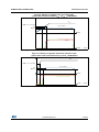
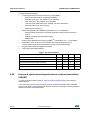
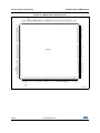
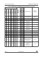
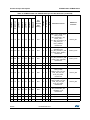
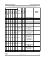
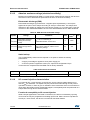
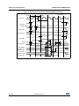
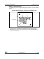
Figure 2 shows the general block diagram of the device family.
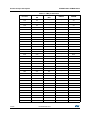
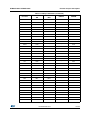
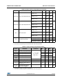
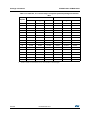
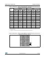
Table 2. STM32F745xx and STM32F746xx features and peripheral counts
DocID027590 Rev 1
Peripherals
Flash memory in Kbytes
SRAM in
Kbytes
512
1024
512
1024
512
1024
512
1024
512
1024
512
System
320(240+16+64)
Instruction
16
Backup
4
FMC memory controller
Ethernet
Timers
STM32F745Vx STM32F746Vx STM32F745Zx STM32F746Zx STM32F745Ix STM32F746Ix STM32F745Bx STM32F746Bx STM32F745Nx STM32F746Nx
1024
512
1024
512
1024
512
1024
512
1024
Yes(1)
Yes
Generalpurpose
10
Advancedcontrol
2
Basic
2
Low-power
1
Random number generator
Yes
Description
13/226
Peripherals
SPI / I2S
STM32F745Vx STM32F746Vx STM32F745Zx STM32F746Zx STM32F745Ix STM32F746Ix STM32F745Bx STM32F746Bx STM32F745Nx STM32F746Nx
4/3 (simplex)(2)
6/3 (simplex)(2)
I2C
4
USART/
UART
4/4
USB OTG
FS
Yes
Communication
interfaces
USB OTG
HS
Yes
CAN
2
SAI
2
SPDIFRX
4 inputs
SDMMC
Yes
DocID027590 Rev 1
Camera interface
LCD-TFT
Yes
No
Yes
No
Yes
Chrom-ART Accelerator™
(DMA2D)
GPIOs
82
114
Yes
No
Yes
No
Yes
140
168
3
16
24
12-bit DAC
Number of channels
Yes
2
216 MHz(3)
Maximum CPU frequency
Ambient temperatures: –40 to +85 °C /–40 to +105 °C
Operating temperatures
Junction temperature: –40 to + 125 °C
LQFP100
WLCSP143
LQFP144
UFBGA176
LQFP176
LQFP208
1.
For the LQFP100 package, only FMC Bank1 is available. Bank1 can only support a multiplexed NOR/PSRAM memory using the NE1 Chip Select.
2.
The SPI1, SPI2 and SPI3 interfaces give the flexibility to work in an exclusive way in either the SPI mode or the I2S audio mode.
TFBGA216
3. 216 MHz maximum frequency for -40°C to + 85°C ambient temperature range (200 MHz maximum frequency for -40°C to + 105°C ambient temperature range).
4.
VDD/VDDA minimum value of 1.7 V is obtained when the internal reset is OFF (refer to Section 2.17.2: Internal reset OFF).
STM32F745xx STM32F746xx
1.7 to 3.6 V(4)
Operating voltage
Package
No
Yes
12-bit ADC
Number of channels
Description
14/226
Table 2. STM32F745xx and STM32F746xx features and peripheral counts (continued)
STM32F745xx STM32F746xx
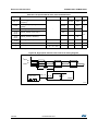
Full compatibility throughout the family
The STM32F745xx and STM32F746xx devices are fully pin-to-pin, compatible with the
STM32F4xxxx devices, allowing the user to try different peripherals, and reaching higher
performances (higher frequency) for a greater degree of freedom during the development
cycle.
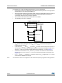
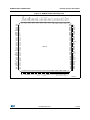
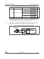
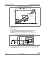
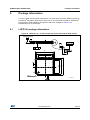
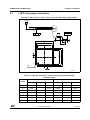
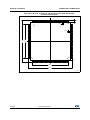
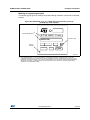
Figure 1 give compatible board designs between the STM32F4xx families.
Figure 1. Compatible board design for LQFP100 package
3&
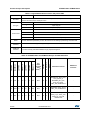
9''
966$
95()
9''$
3$:.83
3$
3$
670)[[670)[[
670)[[670)[[
670)[[670)[[
670)[[670)[[
9''
3%
9&$3
3%
3(
3(
3(
3(
3(
3(
3(
3(
3(
3%
3%
3&
3%
3&
3$
3$
3$
3$
9''
3$
3&
966$
95()
9''$
3$:.83
3$
3$
3$
966
670)[[670)[[
3LQVWRDUHQRWFRPSDWLEOH
9''
966
9&$3
3%
3%
3(
3(
3(
3(
3(
3(
3(
3(
3(
3%
3%
3%
3&
3&
3$
3$
3$
3$
9''
966
1.1
Description
06Y9
The STM32F745xx and STM32F746xx LQFP144, LQFP176, LQFP208, TFBGA216,
UFBGA176, WLCSP143 packages are fully pin to pin compatible with STM32F4xxxx
devices.
DocID027590 Rev 1
15/226
44
Description
STM32F745xx STM32F746xx
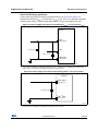
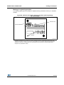
Figure 2. STM32F745xx and STM32F746xx block diagram
:d'Θ^t
DWh
Es/
dDZDϲϰ<
dD
Dͬ
&/&K
Dͬ
Kd',^
&/&K
DϮ
6WUHDPV
),)2
Dϭ
6WUHDPV
),)2
/͕sh^͕^K&
>Ͳd&d
>ͺ,^zE͕>ͺs^zE͕>ͺ͕
ZE'
,^
h^
>ͺZϳ͗Ϭ͕>ͺ'ϳ͗Ϭ͕>ͺϳ͗Ϭ͕
Zd
&>^,ϭD
ϭϬͬϭϬϬ
W,z
h>W/͗<͕ϳ͗Ϭ͕/Z͕^dW͕Eyd
,W
ƚŚĞƌŶĞƚD
D/KĂƐ&
W͕D
ͲĂĐŚĞ
ϰ<
/dDZDϭϲ<
^ZDϮϭϲ<
h^
Kd'&^
,ϮϮϭϲD,nj
E>ϯ͗Ϭ͕^><ϭ͗Ϭ͕^Eϭ͗Ϭ͕
^Et͕E>
EZ^͕E^͕Es
Et/d͕/EdZ
YƵĂĚ^W/
><͕^͕ϯ͗Ϭ
,ϭϮϭϲD,nj
WŽǁĞƌŵĂŶĂŐŵƚ
s
),)2
Wϭϱ͗Ϭ
'W/KWKZd
Wϭϱ͗Ϭ
Λs
^ƵƉƉůLJ
sWϭ͕sWϮ
t<hWϰ͗Ϭ
,^
ƌĞƐĞƚ
ƐƵƉĞƌǀŝƐŝŽŶ
Z
>^
/Ŷƚ
WKZͬWZ
EZ^d
Ws
Λs
ZĞƐĞƚΘ
ĐůŽĐŬ
D E
' d
ĐŽŶƚƌŽů
'W/KWKZd
Λs
'W/KWKZd'
W,ϭϱ͗Ϭ
'W/KWKZd,
K^ͺ/E
ϰͲϮϲD,nj
K^ͺKhd
^ƚĂŶĚďLJ
sdсϭ͘ϲϱƚŽϯ͘ϲs
ŝŶƚĞƌĨĂĐĞ
Λsd
K^ϯϮͺ/E
K^ϯϮͺKhd
yd>ϯϮŬ,nj
>^
W'ϭϱ͗Ϭ
yd>K^
/t'
W><dž
'W/KWKZd&
,><dž
W&ϭϱ͗Ϭ
s͕s^^
KZ
'W/KWKZd
Wϭϱ͗Ϭ
s^^
WKZ
W>>ϭ͕Ϯ͕ϯ
'W/KWKZd
sсϭ͘ϳͬϭ͘ϴƚŽϯ͘ϲs
Z
'W/KWKZd
Wϭϱ͗Ϭ
sh^сϯ͘ϬƚŽϯ͘ϲs
sŽůƚĂŐĞ
ƌĞŐƵůĂƚŽƌ
ϭ͘Ϯs
Λs
;DϮͿ
D
/͕sh^͕^K&
><͕Eϯ͗Ϭ͕Ϯϯ͗Ϭ͕
ϯϭ͗Ϭ͕EKE͕EtE͕
džƚĞƌŶĂůŵĞŵŽƌLJĐŽŶƚƌŽůůĞƌ;&DͿ
^ZD͕^ZD͕W^ZD͕EKZ&ůĂƐŚ͕
EE&ůĂƐŚ
),)2
,ZKDͲZd
Wh/y><͕ϭϯ͗Ϭ
W
^ZDϭϮϰϬ<
>ͺ><
Wϭϱ͗Ϭ
,^zE͕s^zE
ĂŵĞƌĂ
ŝŶƚĞƌĨĂĐĞ
W,z
ϮϭϲD,nj
/ͲĂĐŚĞ
ϰ<
y/D
,h^ͲDdZ/yϭϭ^ϴD
,ďƵƐͲŵĂƚƌŝdžϴ^ϳD
dZϯ͗Ϭ
D//ŽƌZD//ĂƐ&
/dD
ZD
ŽƌƚĞdžͲDϳ
,Ϯy/
dZ<
&/&K
dD
&/&K
:dZ^d͕:d/͕
:d<ͬ^t><
:dKͬ^t͕:dK
Zd
Zdͺ&ϭ
Zdͺ&ϭ
ZdͺϱϬ,
th
W/ϭϱ͗Ϭ
'W/KWKZd/
W:ϭϱ͗Ϭ
'W/KWKZd:
ϰ<<W^ZD
W<ϳ͗Ϭ
'W/KWKZd<
d/DϮ
ϯϮď
ϰĐŚĂŶŶĞůƐ͕dZĂƐ&
d/Dϯ
ϭϲď
ϰĐŚĂŶŶĞůƐ͕dZĂƐ&
d/Dϰ
ϭϲď
ϰĐŚĂŶŶĞůƐ͕dZĂƐ&
ϰĐŚĂŶŶĞůƐ
>^
ĂĐŬƵƉƌĞŐŝƐƚĞƌ
Dϭ
DϮ
yd/d͘t<hW
^DDϭ
,ͬWϭ
,ͬWϮ
ϰĐŽŵƉů͘ĐŚĂŶ͘;d/Dϭͺ,ϭϭ͗ϰEͿ͕
ϰĐŚĂŶ͘;d/Dϭͺ,ϭϭ͗ϰdZ͕
d/DϭͬWtD
d/DϴͬWtD
ϰĐŚĂŶ͘;d/Dϴͺ,ϭϭ͗ϰ͕dZ͕
</EĂƐ&
d/Dϵ
ϭĐŚĂŶŶĞůĂƐ&
d/DϭϬ
ŝƌ
ƐŵĐĂƌĚ
ŝƌ
ϭϲď
h^Zdϭ
h^Zdϲ
^W/ϰ
^W/ϱ
^͕^<͕&^͕D><ĂƐ&
^/Ϯ
ϭϲď
d/Dϳ
ϭϲď
/d&
Ϯ
ƚŽƚŚĞϭΘϮ
ϯ
/&
/&
ͺKhdϭ
ĂƐ&
ͺKhdϮ
ĂƐ&
d^͕Zd^ĂƐ&
Zy͕dyĂƐ&
Zy͕dyĂƐ&
hZdϳ
Zy͕dyĂƐ&
Zy͕dyĂƐ&
hZdϴ
^W/Ϯͬ/Ϯ^Ϯ
DK^/ͬ^͕^<ͬ<
E^^ͬt^͕D<ĂƐ&
^W/ϯͬ/Ϯ^ϯ
DK^/ͬ^͕^<ͬ<
/Ϯϭͬ^Dh^
E^^ͬt^͕D<ĂƐ&
^>͕^͕^DĂƐ&
^>͕^͕^DĂƐ&
^>͕^͕^DĂƐ&
^>͕^͕^DĂƐ&
dy͕Zy
ďdžEϭ
ďdžEϮ
ϭ
d^͕Zd^ĂƐ&
Zy͕dyĂƐ&
ŝƌ
/Ϯϰͬ^Dh^
ƵĂů
ĐŚĂŶŶĞůƐ
h ^dĞŵƉĞƌĂƚƵƌĞƐĞŶƐŽƌ
Z d Ϯ D Ɖ Ɛ
ŝƌ
ƐŵĐĂƌĚ
hZdϱ
/Ϯϯͬ^Dh^
Λs
Zy͕dyĂƐ&
ƐŵĐĂƌĚ
hZdϰ
/ϮϮͬ^Dh^
Λs
ϴĂŶĂůŽŐŝŶƉƵƚƐĨŽƌϯ
d/Dϲ
^W/ϲ
^/ϭ
ƚŽƚŚĞϯƐ
ϭϲď
>Wd/Dϭ
^W/ϭͬ/Ϯ^ϭ
^͕^<͕&^͕D><ĂƐ&
ϴĂŶĂůŽŐŝŶƉƵƚƐĐŽŵŵŽŶ
ϭĐŚĂŶŶĞůĂƐ&
h^ZdϮ
W ϭϬ D,nj
ϯ
WϭϱϰD,nj;ŵĂdžͿ
ƐŵĐĂƌĚ
DK^/͕D/^K͕
^<͕E^^ĂƐ&
DK^/͕D/^K͕
^<͕E^^ĂƐ&
DK^/͕D/^K͕
^<͕E^^ĂƐ&
ϴĂŶĂůŽŐŝŶƉƵƚƐĐŽŵŵŽŶ
ϭϲď
tt'
ϭϲď
WϮϭϬϴD,nj;ŵĂdžͿ
d/Dϭϭ
DK^/ͬ^͕^<ͬ<
E^^ͬt^͕D<ĂƐ&
sZ&ͺ
ϭĐŚĂŶŶĞůĂƐ&
ϭϲď
W Ϯ ϲϬ D ,nj
d^͕Zd^ĂƐ&
ϭϲď
ϭϲď
&/&K &/&K
Zy͕dy͕<͕
ϮĐŚĂŶŶĞůƐĂƐ&
d/Dϭϯ
h^Zdϯ
ϭĐŚĂŶŶĞůĂƐ&
d^͕Zd^ĂƐ&
ϭϲď
d/Dϭϰ
ϮĐŚĂŶŶĞůƐĂƐ&
Zy͕dy͕<͕
ϯϮď
ϭϲď
</EĂƐ&
ϰĐŽŵƉů͘ĐŚĂŶ͘;d/Dϴͺ,ϭϭ͗ϰEͿ͕
d/Dϱ
d/DϭϮ
ŝŐŝƚĂůĨŝůƚĞƌ
D͕<ĂƐ&
&/&K
ϳ͗Ϭ
&/&K
ϭϲϴ&
dy͕Zy
^W/&Zy
^W/&Zyϯ͗ϬĂƐ&
,D/Ͳ
,D/ͺĂƐ&
06Y9
1. The timers connected to APB2 are clocked from TIMxCLK up to 216 MHz, while the timers connected to APB1 are clocked
from TIMxCLK either up to 108 MHz or 216 MHz depending on TIMPRE bit configuration in the RCC_DCKCFGR register.
16/226
DocID027590 Rev 1
STM32F745xx STM32F746xx
Functional overview
2
Functional overview
2.1
ARM® Cortex®-M7 with FPU
The ARM® Cortex®-M7 with FPU processor is the latest generation of ARM processors for
embedded systems. It was developed to provide a low-cost platform that meets the needs of
MCU implementation, with a reduced pin count and a low-power consumption, while
delivering an outstanding computational performance and low interrupt latency.
The Cortex®-M7 processor is a highly efficient high-performance featuring:
–
Six-stage dual-issue pipeline
–
Dynamic branch prediction
–
Harvard caches (4kB of I-cache and 4kB of D-cache)
–
64-bit AXI4 interface
–
64-bit ITCM interface
–
2x32-bit DTCM interfaces
The processor supports the following memory interfaces:
•
Tightly Coupled Memory (TCM) interface.
•
Harvard instruction and data caches and AXI master (AXIM) interface.
•
Dedicated low-latency AHB-Lite peripheral (AHBP) interface.
The processor supports a set of DSP instructions which allow efficient signal processing and
complex algorithm execution.
Its single precision FPU (floating point unit) speeds up the software development by using
metalanguage development tools, while avoiding saturation.
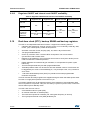
Figure 2 shows the general block diagram of the STM32F756xx family.
Note:
Cortex®-M7 with FPU core is binary compatible with the Cortex®-M4 core.
2.2
Memory protection unit
The memory protection unit (MPU) is used to manage the CPU accesses to memory to
prevent one task to accidentally corrupt the memory or resources used by any other active
task. This memory area is organized into up to 8 protected areas that can in turn be divided
up into 8 subareas. The protection area sizes are between 32 bytes and the whole 4
gigabytes of addressable memory.
The MPU is especially helpful for applications where some critical or certified code has to be
protected against the misbehavior of other tasks. It is usually managed by an RTOS (realtime operating system). If a program accesses a memory location that is prohibited by the
MPU, the RTOS can detect it and take action. In an RTOS environment, the kernel can
dynamically update the MPU area setting, based on the process to be executed.
The MPU is optional and can be bypassed for applications that do not need it.
DocID027590 Rev 1
17/226
44
Functional overview
2.3
STM32F745xx STM32F746xx
Embedded Flash memory
The STM32F745xx and STM32F746xx devices embed a Flash memory of up to 1 Mbytes
available for storing programs and data.
2.4
CRC (cyclic redundancy check) calculation unit
The CRC (cyclic redundancy check) calculation unit is used to get a CRC code using a
configurable generator polynomial value and size.
Among other applications, CRC-based techniques are used to verify the data transmission
or storage integrity. In the scope of the EN/IEC 60335-1 standard, they offer a mean of
verifying the Flash memory integrity. The CRC calculation unit helps to compute a signature
of the software during runtime, to be compared with a reference signature generated at linktime and stored at a given memory location.
2.5
Embedded SRAM
All the devices features:
•
•
System SRAM up to 320Kbytes:
–
SRAM1 on AHB bus Matrix: 240Kbytes
–
SRAM2 on AHB bus Matrix: 16Kbytes
–
DTCM-RAM on TCM interface (Tighly Coupled Memory interface): 64 Kbytes for
critical real time data.
Instruction RAM (ITCM-RAM) 16Kbytes:
–
It is mapped on TCM interface and reserved only for CPU Execution/Instruction
useful for critical real time routines.
The Data TCM RAM is accessible by the GP-DMAs and peripherals DMAs through specific
AHB slave of the CPU.The TCM RAM instruction is reserved only for CPU. It is accessed at
CPU clock speed with 0-wait states.
•
4 Kbytes of backup SRAM
This area is accessible only from the CPU. Its content is protected against possible
unwanted write accesses, and is retained in Standby or VBAT mode.
2.6
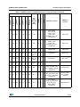
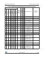
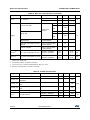
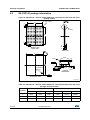
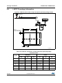
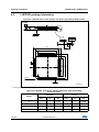
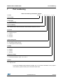
AXI-AHB bus matrix
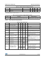
The STM32F745xx and STM32F746xx system architecture is based on 2 sub-systems:
•
•
An AXI to multi AHB bridge converting AXI4 protocol to AHB-Lite protocol:
–
3x AXI to 32-bit AHB bridges connected to AHB bus matrix
–
1x AXI to 64-bit AHB bridge connected to the embedded flash
A multi-AHB Bus-Matrix:
–
18/226
The 32-bit multi-AHB bus matrix interconnects all the masters (CPU, DMAs,
Ethernet, USB HS, LCD-TFT, and DMA2D) and the slaves (Flash memory, RAM,
FMC, Quad SPI, AHB and APB peripherals) and ensures a seamless and an
efficient operation even when several high-speed peripherals work
simultaneously.
DocID027590 Rev 1
STM32F745xx STM32F746xx
Functional overview
,^
ŚƌŽŵͲZd
ĐĐĞůĞƌĂƚŽƌ
;DϮͿ
DϮ
>Ͳd&dͺD
h^ͺ,^ͺD
DͺWϮ
d,ZEdͺD
,W
y/D
.%
,'&DFKH
'W
D
h^Kd' >Ͳd&d
DϮ ƚŚĞƌŶĞƚ
,^
DͺDDϮ
DͺW/
ZDŽƌƚĞdžͲDϳ
'W
Dϭ
DͺDDϭ
/dD
dD
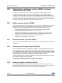
Figure 3. STM32F745xx and STM32F746xx AXI-AHB bus matrix architecture
dDZD
ϲϰ<
/dDZD
ϭϲ<
y/ƚŽ
ŵƵůƚŝͲ,
Zd
/dD
ϲϰͲďŝƚ,
&>^,
ϭD
ϲϰͲďŝƚƵ^DĂƚƌŝdž
^ZDϭ
ϮϰϬ<
^ZDϮ
ϭϲ<
,
WĞƌŝƉŚϭ
,
ƉĞƌŝƉŚϮ
&DĞdžƚĞƌŶĂů
DĞŵƚů
Wϭ
WϮ
YƵĂĚ^W/
ϯϮͲďŝƚƵƐDĂƚƌŝdžͲ^
069
1. The above figure has large wires for 64-bits bus and thin wires for 32-bits bus.
2.7
DMA controller (DMA)
The devices feature two general-purpose dual-port DMAs (DMA1 and DMA2) with 8
streams each. They are able to manage memory-to-memory, peripheral-to-memory and
memory-to-peripheral transfers. They feature dedicated FIFOs for APB/AHB peripherals,
support burst transfer and are designed to provide the maximum peripheral bandwidth
(AHB/APB).
The two DMA controllers support circular buffer management, so that no specific code is
needed when the controller reaches the end of the buffer. The two DMA controllers also
have a double buffering feature, which automates the use and switching of two memory
buffers without requiring any special code.
DocID027590 Rev 1
19/226
44
Functional overview
STM32F745xx STM32F746xx
Each stream is connected to dedicated hardware DMA requests, with support for software
trigger on each stream. Configuration is made by software and transfer sizes between
source and destination are independent.
The DMA can be used with the main peripherals:
2.8
•
SPI and I2S
•
I2C
•
USART
•
General-purpose, basic and advanced-control timers TIMx
•
DAC
•
SDMMC
•
Camera interface (DCMI)
•
ADC
•
SAI
•
SPDIFRX
•
Quad SPI
•
HDMI-CEC
Flexible memory controller (FMC)
The Flexible memory controller (FMC) includes three memory controllers:
•
The NOR/PSRAM memory controller
•
The NAND/memory controller
•
The Synchronous DRAM (SDRAM/Mobile LPSDR SDRAM) controller
The main features of the FMC controller are the following:
•
Interface with static-memory mapped devices including:
–
Static random access memory (SRAM)
–
NOR Flash memory/OneNAND Flash memory
–
PSRAM (4 memory banks)
–
NAND Flash memory with ECC hardware to check up to 8 Kbytes of data
•
Interface with synchronous DRAM (SDRAM/Mobile LPSDR SDRAM) memories
•
8-,16-,32-bit data bus width
•
Independent Chip Select control for each memory bank
•
Independent configuration for each memory bank
•
Write FIFO
•
Read FIFO for SDRAM controller
•
The Maximum FMC_CLK/FMC_SDCLK frequency for synchronous accesses is
HCLK/2.
LCD parallel interface
The FMC can be configured to interface seamlessly with most graphic LCD controllers. It
supports the Intel 8080 and Motorola 6800 modes, and is flexible enough to adapt to
20/226
DocID027590 Rev 1
STM32F745xx STM32F746xx
Functional overview
specific LCD interfaces. This LCD parallel interface capability makes it easy to build costeffective graphic applications using LCD modules with embedded controllers or high
performance solutions using external controllers with dedicated acceleration.
2.9
Quad SPI memory interface (QUADSPI)
All STM32F75xx devices embed a Quad SPI memory interface, which is a specialized
communication interface targetting Single, Dual or Quad SPI flash memories. It can work in:
•
Direct mode through registers.
•
External flash status register polling mode.
•
Memory mapped mode.
Up to 256 Mbytes external flash are memory mapped, supporting 8, 16 and 32-bit access.
Code execution is supported.
The opcode and the frame format are fully programmable. Communication can be either in
Single Data Rate or Dual Data Rate.
2.10
LCD-TFT controller
The LCD-TFT display controller provides a 24-bit parallel digital RGB (Red, Green, Blue)
and delivers all signals to interface directly to a broad range of LCD and TFT panels up to
XGA (1024x768) resolution with the following features:
2.11
•
2 displays layers with dedicated FIFO (64x32-bit)
•
Color Look-Up table (CLUT) up to 256 colors (256x24-bit) per layer
•
Up to 8 Input color formats selectable per layer
•
Flexible blending between two layers using alpha value (per pixel or constant)
•
Flexible programmable parameters for each layer
•
Color keying (transparency color)
•
Up to 4 programmable interrupt events.
Chrom-ART Accelerator™ (DMA2D)
The Chrom-Art Accelerator™ (DMA2D) is a graphic accelerator which offers advanced bit
blitting, row data copy and pixel format conversion. It supports the following functions:
•
Rectangle filling with a fixed color
•
Rectangle copy
•
Rectangle copy with pixel format conversion
•
Rectangle composition with blending and pixel format conversion.
Various image format coding are supported, from indirect 4bpp color mode up to 32bpp
direct color. It embeds dedicated memory to store color lookup tables.
An interrupt can be generated when an operation is complete or at a programmed
watermark.
All the operations are fully automatized and are running independently from the CPU or the
DMAs.
DocID027590 Rev 1
21/226
44
Functional overview
2.12
STM32F745xx STM32F746xx
Nested vectored interrupt controller (NVIC)
The devices embed a nested vectored interrupt controller able to manage 16 priority levels,
and handle up to 97 maskable interrupt channels plus the 16 interrupt lines of the Cortex®M7 with FPU core.
•
Closely coupled NVIC gives low-latency interrupt processing
•
Interrupt entry vector table address passed directly to the core
•
Allows early processing of interrupts
•
Processing of late arriving, higher-priority interrupts
•
Support tail chaining
•
Processor state automatically saved
•
Interrupt entry restored on interrupt exit with no instruction overhead
This hardware block provides flexible interrupt management features with minimum interrupt
latency.
2.13
External interrupt/event controller (EXTI)
The external interrupt/event controller consists of 24 edge-detector lines used to generate
interrupt/event requests. Each line can be independently configured to select the trigger
event (rising edge, falling edge, both) and can be masked independently. A pending register
maintains the status of the interrupt requests. The EXTI can detect an external line with a
pulse width shorter than the Internal APB2 clock period. Up to 168 GPIOs can be connected
to the 16 external interrupt lines.
2.14
Clocks and startup
On reset the 16 MHz internal HSI RC oscillator is selected as the default CPU clock. The
16 MHz internal RC oscillator is factory-trimmed to offer 1% accuracy. The application can
then select as system clock either the RC oscillator or an external 4-26 MHz clock source.
This clock can be monitored for failure. If a failure is detected, the system automatically
switches back to the internal RC oscillator and a software interrupt is generated (if enabled).
This clock source is input to a PLL thus allowing to increase the frequency up to 216 MHz.
Similarly, full interrupt management of the PLL clock entry is available when necessary (for
example if an indirectly used external oscillator fails).
Several prescalers allow the configuration of the two AHB buses, the high-speed APB
(APB2) and the low-speed APB (APB1) domains. The maximum frequency of the two AHB
buses is 216 MHz while the maximum frequency of the high-speed APB domains is
108 MHz. The maximum allowed frequency of the low-speed APB domain is 54 MHz.
The devices embed two dedicated PLL (PLLI2S and PLLSAI) which allow to achieve audio
class performance. In this case, the I2S and SAI master clock can generate all standard
sampling frequencies from 8 kHz to 192 kHz.
22/226
DocID027590 Rev 1
STM32F745xx STM32F746xx
2.15
Functional overview
Boot modes
At startup, the boot memory space is selected by the BOOT pin and BOOT_ADDx option
bytes, allowing to program any boot memory address from 0x0000 0000 to 0x3FFF FFFF
which includes:
•
All Flash address space mapped on ITCM or AXIM interface
•
All RAM address space: ITCM, DTCM RAMs and SRAMs mapped on AXIM interface
•
The System memory bootloader
The boot loader is located in system memory. It is used to reprogram the Flash memory
through a serial interface.
2.16
Note:
Power supply schemes
•
VBAT = 1.65 to 3.6 V: power supply for RTC, external clock 32 kHz oscillator and
backup registers (through power switch) when VDD is not present.
•
VDD = 1.7 to 3.6 Vexternal power supply for I/Os and the internal regulator (when
enabled), provided externally through VDD pins.
•
VSSA, VDDA = 1.7 to 3.6 V: external analog power supplies for ADC, DAC, reset blocks,
RCs and PLL. VDDA and VSSA must be connected to VDD and VSS, respectively.
VDD/VDDA minimum value of 1.7 V is obtained when the internal reset is OFF (refer to
Section 2.17.2: Internal reset OFF). Refer to Table 3: Voltage regulator configuration mode
versus device operating mode to identify the packages supporting this option.
•
VDDUSB can be connected either to VDD or an external independent power supply (3.0
to 3.6V) for USB transceivers (refer to Figure 4 and Figure 5). For example, when
device is powered at 1.8V, an independent power supply 3.3V can be connected to
VDDUSB. When the VDDUSB is connected to a separated power supply, it is independent
from VDD or VDDA but it must be the last supply to be provided and the first to
disappear. The following conditions VDDUSB must be respected:
–
During power-on phase (VDD < VDD_MIN), VDDUSB should be always lower than
VDD
–
During power-down phase (VDD < VDD_MIN), VDDUSB should be always lower than
VDD
–
VDDSUB rising and falling time rate specifications must be respected (see Table 21
and Table 22)
–
In operating mode phase, VDDUSB could be lower or higher than VDD:
- If USB (USB OTG_HS/OTG_FS) is used, the associated GPIOs powered by
VDDUSB are operating between VDDUSB_MIN and VDDUSB_MAX.
- The VDDUSB supply both USB transceiver (USB OTG_HS and USB OTG_FS). If
only one USB transceiver is used in the application, the GPIOs associated to the
other USB transceiver are still supplied by VDDUSB.
- If USB (USB OTG_HS/OTG_FS) is not used, the associated GPIOs powered by
VDDUSB are operating between VDD_MIN and VDD_MAX.
DocID027590 Rev 1
23/226
44
Functional overview
STM32F745xx STM32F746xx
Figure 4. VDDUSB connected to VDD power supply
9''
9''B0$;
9'' 9''$ 9''86%
9''B0,1
2SHUDWLQJPRGH
3RZHURQ
3RZHUGRZQ
WLPH
069
Figure 5. VDDUSB connected to external power supply
9''86%B0$;
86% IXQFWLRQDODUHD
9''86%
9''86%B0,1
86%QRQ
IXQFWLRQDO
DUHD
9'' 9''$
86%QRQ
IXQFWLRQDO
DUHD
2SHUDWLQJPRGH
3RZHUGRZQ
9''B0,1
3RZHURQ
WLPH
069
2.17
Power supply supervisor
2.17.1
Internal reset ON
On packages embedding the PDR_ON pin, the power supply supervisor is enabled by
holding PDR_ON high. On the other packages, the power supply supervisor is always
enabled.
The device has an integrated power-on reset (POR)/ power-down reset (PDR) circuitry
coupled with a Brownout reset (BOR) circuitry. At power-on, POR/PDR is always active and
ensures proper operation starting from 1.8 V. After the 1.8 V POR threshold level is
24/226
DocID027590 Rev 1
STM32F745xx STM32F746xx
Functional overview
reached, the option byte loading process starts, either to confirm or modify default BOR
thresholds, or to disable BOR permanently. Three BOR thresholds are available through
option bytes. The device remains in reset mode when VDD is below a specified threshold,
VPOR/PDR or VBOR, without the need for an external reset circuit.
The device also features an embedded programmable voltage detector (PVD) that monitors
the VDD/VDDA power supply and compares it to the VPVD threshold. An interrupt can be
generated when VDD/VDDA drops below the VPVD threshold and/or when VDD/VDDA is
higher than the VPVD threshold. The interrupt service routine can then generate a warning
message and/or put the MCU into a safe state. The PVD is enabled by software.
2.17.2
Internal reset OFF
This feature is available only on packages featuring the PDR_ON pin. The internal power-on
reset (POR) / power-down reset (PDR) circuitry is disabled through the PDR_ON pin.
An external power supply supervisor should monitor VDD and should maintain the device in
reset mode as long as VDD is below a specified threshold. PDR_ON should be connected to
VSS. Refer to Figure 6: Power supply supervisor interconnection with internal reset OFF.
Figure 6. Power supply supervisor interconnection with internal reset OFF
9''
$SSOLFDWLRQUHVHW
VLJQDORSWLRQDO
9%$7
3'5B21
966
3'5QRWDFWLYHY9''Y
06Y9
The VDD specified threshold, below which the device must be maintained under reset, is
1.7 V (see Figure 7).
A comprehensive set of power-saving mode allows to design low-power applications.
When the internal reset is OFF, the following integrated features are no more supported:
•
The integrated power-on reset (POR) / power-down reset (PDR) circuitry is disabled
•
The brownout reset (BOR) circuitry must be disabled
•
The embedded programmable voltage detector (PVD) is disabled
•
VBAT functionality is no more available and VBAT pin should be connected to VDD.
All the packages, except for the LQFP100, allow to disable the internal reset through the
PDR_ON signal when connected to VSS.
DocID027590 Rev 1
25/226
44
Functional overview
STM32F745xx STM32F746xx
Figure 7. PDR_ON control with internal reset OFF
9 ''
3'5 9
WLPH
5HVHWE\RWKHUVRXUFHWKDQ
SRZHUVXSSO\VXSHUYLVRU
1567
3'5B21
3'5B21
WLPH
069
2.18
Voltage regulator
The regulator has four operating modes:
•
•
2.18.1
Regulator ON
–
Main regulator mode (MR)
–
Low-power regulator (LPR)
–
Power-down
Regulator OFF
Regulator ON
On packages embedding the BYPASS_REG pin, the regulator is enabled by holding
BYPASS_REG low. On all other packages, the regulator is always enabled.
There are three power modes configured by software when the regulator is ON:
•
MR mode used in Run/sleep modes or in Stop modes
–
In Run/Sleep mode
The MR mode is used either in the normal mode (default mode) or the over-drive
mode (enabled by software). Different voltages scaling are provided to reach the
best compromise between the maximum frequency and dynamic power
26/226
DocID027590 Rev 1
STM32F745xx STM32F746xx
Functional overview
consumption. The over-drive mode allows operating at a higher frequency than
the normal mode for a given voltage scaling.
–
In Stop modes
The MR can be configured in two ways during Stop mode:
MR operates in normal mode (default mode of MR in Stop mode)
MR operates in under-drive mode (reduced leakage mode).
•
LPR is used in the Stop modes:
The LP regulator mode is configured by software when entering Stop mode.
Like the MR mode, the LPR can be configured in two ways during Stop mode:
•
–
LPR operates in normal mode (default mode when LPR is ON)
–
LPR operates in under-drive mode (reduced leakage mode).
Power-down is used in Standby mode.
The Power-down mode is activated only when entering in Standby mode. The regulator
output is in high impedance and the kernel circuitry is powered down, inducing zero
consumption. The contents of the registers and SRAM are lost.
Refer to Table 3 for a summary of voltage regulator modes versus device operating modes.
Two external ceramic capacitors should be connected on VCAP_1 and VCAP_2 pin.
All packages have the regulator ON feature.
Table 3. Voltage regulator configuration mode versus device operating mode(1)
Voltage regulator
configuration
Run mode
Sleep mode
Stop mode
Standby mode
Normal mode
MR
MR
MR or LPR
-
Over-drive
mode(2)
MR
MR
-
-
Under-drive mode
-
-
MR or LPR
-
Power-down mode
-
-
-
Yes
1. ‘-’ means that the corresponding configuration is not available.
2. The over-drive mode is not available when VDD = 1.7 to 2.1 V.
2.18.2
Regulator OFF
This feature is available only on packages featuring the BYPASS_REG pin. The regulator is
disabled by holding BYPASS_REG high. The regulator OFF mode allows to supply
externally a V12 voltage source through VCAP_1 and VCAP_2 pins.
Since the internal voltage scaling is not managed internally, the external voltage value must
be aligned with the targeted maximum frequency.The two 2.2 µF ceramic capacitors should
be replaced by two 100 nF decoupling capacitors.
When the regulator is OFF, there is no more internal monitoring on V12. An external power
supply supervisor should be used to monitor the V12 of the logic power domain. PA0 pin
should be used for this purpose, and act as power-on reset on V12 power domain.
DocID027590 Rev 1
27/226
44
Functional overview
STM32F745xx STM32F746xx
In regulator OFF mode, the following features are no more supported:
•
PA0 cannot be used as a GPIO pin since it allows to reset a part of the V12 logic power
domain which is not reset by the NRST pin.
•
As long as PA0 is kept low, the debug mode cannot be used under power-on reset. As
a consequence, PA0 and NRST pins must be managed separately if the debug
connection under reset or pre-reset is required.
•
The over-drive and under-drive modes are not available.
•
The Standby mode is not available.
Figure 8. Regulator OFF
9
([WHUQDO9&$3BSRZHU
$SSOLFDWLRQUHVHW
VXSSO\VXSHUYLVRU
([WUHVHWFRQWUROOHUDFWLYH VLJQDORSWLRQDO
ZKHQ9&$3B0LQ9
9''
3$
9''
1567
%<3$66B5(*
9
9&$3B
9&$3B
DL9
The following conditions must be respected:
Note:
28/226
•
VDD should always be higher than VCAP_1 and VCAP_2 to avoid current injection
between power domains.
•
If the time for VCAP_1 and VCAP_2 to reach V12 minimum value is faster than the time for
VDD to reach 1.7 V, then PA0 should be kept low to cover both conditions: until VCAP_1
and VCAP_2 reach V12 minimum value and until VDD reaches 1.7 V (see Figure 9).
•
Otherwise, if the time for VCAP_1 and VCAP_2 to reach V12 minimum value is slower
than the time for VDD to reach 1.7 V, then PA0 could be asserted low externally (see
Figure 10).
•
If VCAP_1 and VCAP_2 go below V12 minimum value and VDD is higher than 1.7 V, then a
reset must be asserted on PA0 pin.
The minimum value of V12 depends on the maximum frequency targeted in the application.
DocID027590 Rev 1
STM32F745xx STM32F746xx
Functional overview
Figure 9. Startup in regulator OFF: slow VDD slope
- power-down reset risen after VCAP_1/VCAP_2 stabilization
9''
3'5 9RU9
9
0LQ9
9&$3B9&$3B
WLPH
1567
WLPH
DLI
1. This figure is valid whatever the internal reset mode (ON or OFF).
Figure 10. Startup in regulator OFF mode: fast VDD slope
- power-down reset risen before VCAP_1/VCAP_2 stabilization
9''
3'5 9RU9
9&$3B9&$3B
9
0LQ9
1567
WLPH
3$DVVHUWHGH[WHUQDOO\
WLPH
DLH
1. This figure is valid whatever the internal reset mode (ON or OFF).
DocID027590 Rev 1
29/226
44
Functional overview
2.18.3
STM32F745xx STM32F746xx
Regulator ON/OFF and internal reset ON/OFF availability
Table 4. Regulator ON/OFF and internal reset ON/OFF availability
Package
Regulator ON
Regulator OFF
Internal reset ON Internal reset OFF
LQFP100
LQFP144,
LQFP208
LQFP176,
WLCSP143,
UFBGA176,
TFBGA216
2.19
Yes
Yes
No
Yes
PDR_ON set to
VDD
Yes
PDR_ON set to
VSS
No
Yes
Yes
BYPASS_REG set BYPASS_REG set
to VDD
to VSS
Real-time clock (RTC), backup SRAM and backup registers
The RTC is an independent BCD timer/counter. It supports the following features:
•
Calendar with subsecond, seconds, minutes, hours (12 or 24 format), week day, date,
month, year, in BCD (binary-coded decimal) format.
•
Automatic correction for 28, 29 (leap year), 30, and 31 days of the month.
•
Two programmable alarms.
•
On-the-fly correction from 1 to 32767 RTC clock pulses. This can be used to
synchronize it with a master clock.
•
Reference clock detection: a more precise second source clock (50 or 60 Hz) can be
used to enhance the calendar precision.
•
Digital calibration circuit with 0.95 ppm resolution, to compensate for quartz crystal
inaccuracy.
•
Three anti-tamper detection pins with programmable filter.
•
Timestamp feature which can be used to save the calendar content. This function can
be triggered by an event on the timestamp pin, or by a tamper event, or by a switch to
VBAT mode.
•
17-bit auto-reload wakeup timer (WUT) for periodic events with programmable
resolution and period.
The RTC and the 32 backup registers are supplied through a switch that takes power either
from the VDD supply when present or from the VBAT pin.
The backup registers are 32-bit registers used to store 128 bytes of user application data
when VDD power is not present. They are not reset by a system or power reset, or when the
device wakes up from Standby mode.
The RTC clock sources can be:
30/226
•
A 32.768 kHz external crystal (LSE)
•
An external resonator or oscillator(LSE)
•
The internal low-power RC oscillator (LSI, with typical frequency of 32 kHz)
•
The high-speed external clock (HSE) divided by 32.
DocID027590 Rev 1
STM32F745xx STM32F746xx
Functional overview
The RTC is functional in VBAT mode and in all low-power modes when it is clocked by the
LSE. When clocked by the LSI, the RTC is not functional in VBAT mode, but is functional in
all low-power modes.
All RTC events (Alarm, WakeUp Timer, Timestamp or Tamper) can generate an interrupt
and wakeup the device from the low-power modes.
2.20
Low-power modes
The devices support three low-power modes to achieve the best compromise between lowpower consumption, short startup time and available wakeup sources:
•
Sleep mode
In Sleep mode, only the CPU is stopped. All peripherals continue to operate and can
wake up the CPU when an interrupt/event occurs.
•
Stop mode
The Stop mode achieves the lowest power consumption while retaining the contents of
SRAM and registers. All clocks in the 1.2 V domain are stopped, the PLL, the HSI RC
and the HSE crystal oscillators are disabled.
The voltage regulator can be put either in main regulator mode (MR) or in low-power
mode (LPR). Both modes can be configured as follows (see Table 5: Voltage regulator
modes in Stop mode):
–
Normal mode (default mode when MR or LPR is enabled)
–
Under-drive mode.
The device can be woken up from the Stop mode by any of the EXTI line (the EXTI line
source can be one of the 16 external lines, the PVD output, the RTC alarm / wakeup /
tamper / time stamp events, the USB OTG FS/HS wakeup or the Ethernet wakeup and
LPTIM1 asynchronous interrupt).
Table 5. Voltage regulator modes in Stop mode
•
Voltage regulator
configuration
Main regulator (MR)
Low-power regulator (LPR)
Normal mode
MR ON
LPR ON
Under-drive mode
MR in under-drive mode
LPR in under-drive mode
Standby mode
The Standby mode is used to achieve the lowest power consumption. The internal
voltage regulator is switched off so that the entire 1.2 V domain is powered off. The
PLL, the HSI RC and the HSE crystal oscillators are also switched off. After entering
Standby mode, the SRAM and register contents are lost except for registers in the
backup domain and the backup SRAM when selected.
The device exits the Standby mode when an external reset (NRST pin), an IWDG reset,
a rising or falling edge on one of the 6 WKUP pins (PA0, PA2, PC1, PC13, PI8, PI11),
or an RTC alarm / wakeup / tamper /time stamp event occurs.
The Standby mode is not supported when the embedded voltage regulator is bypassed
and the 1.2 V domain is controlled by an external power.
DocID027590 Rev 1
31/226
44
Functional overview
2.21
STM32F745xx STM32F746xx
VBAT operation
The VBAT pin allows to power the device VBAT domain from an external battery, an external
supercapacitor, or from VDD when no external battery and an external supercapacitor are
present.
VBAT operation is activated when VDD is not present.
The VBAT pin supplies the RTC, the backup registers and the backup SRAM.
Note:
When the microcontroller is supplied from VBAT, external interrupts and RTC alarm/events
do not exit it from VBAT operation.
When PDR_ON pin is connected to VSS (Internal Reset OFF), the VBAT functionality is no
more available and VBAT pin should be connected to VDD.
2.22
Timers and watchdogs
The devices include two advanced-control timers, eight general-purpose timers, two basic
timers and two watchdog timers.
All timer counters can be frozen in debug mode.
Table 6 compares the features of the advanced-control, general-purpose and basic timers.
32/226
DocID027590 Rev 1
STM32F745xx STM32F746xx
Functional overview
Table 6. Timer feature comparison
Timer
type
Advance
d-control
Timer
TIM1,
TIM8
TIM2,
TIM5
TIM3,
TIM4
TIM9
DMA
Capture/ Complem
Counter Counter Prescaler
request
compare
entary
resolution
type
factor
generation channels
output
TIM12
TIM13,
TIM14
Basic
TIM6,
TIM7
(1)
16-bit
Any
Up,
integer
Down,
between 1
Up/down
and 65536
Yes
4
Yes
108
216
32-bit
Any
Up,
integer
Down,
between 1
Up/down
and 65536
Yes
4
No
54
108/216
16-bit
Any
Up,
integer
Down,
between 1
Up/down
and 65536
Yes
4
No
54
108/216
16-bit
Up
Any
integer
between 1
and 65536
No
2
No
108
216
Up
Any
integer
between 1
and 65536
No
1
No
108
216
Up
Any
integer
between 1
and 65536
No
2
No
54
108/216
Up
Any
integer
between 1
and 65536
No
1
No
54
108/216
Up
Any
integer
between 1
and 65536
Yes
0
No
54
108/216
General
purpose
TIM10,
TIM11
Max
timer
clock
(MHz)
Max
interfac
e clock
(MHz)
16-bit
16-bit
16-bit
16-bit
1. The maximum timer clock is either 108 or 216 MHz depending on TIMPRE bit configuration in the RCC_DCKCFGR
register.
2.22.1
Advanced-control timers (TIM1, TIM8)
The advanced-control timers (TIM1, TIM8) can be seen as three-phase PWM generators
multiplexed on 6 channels. They have complementary PWM outputs with programmable
DocID027590 Rev 1
33/226
44
Functional overview
STM32F745xx STM32F746xx
inserted dead times. They can also be considered as complete general-purpose timers.
Their 4 independent channels can be used for:
•
Input capture
•
Output compare
•
PWM generation (edge- or center-aligned modes)
•
One-pulse mode output
If configured as standard 16-bit timers, they have the same features as the general-purpose
TIMx timers. If configured as 16-bit PWM generators, they have full modulation capability (0100%).
The advanced-control timer can work together with the TIMx timers via the Timer Link
feature for synchronization or event chaining.
TIM1 and TIM8 support independent DMA request generation.
2.22.2
General-purpose timers (TIMx)
There are ten synchronizable general-purpose timers embedded in the STM32F756xx
devices (see Table 6 for differences).
•
TIM2, TIM3, TIM4, TIM5
The STM32F756xx include 4 full-featured general-purpose timers: TIM2, TIM5, TIM3,
and TIM4.The TIM2 and TIM5 timers are based on a 32-bit auto-reload
up/downcounter and a 16-bit prescaler. The TIM3 and TIM4 timers are based on a 16bit auto-reload up/downcounter and a 16-bit prescaler. They all feature 4 independent
channels for input capture/output compare, PWM or one-pulse mode output. This gives
up to 16 input capture/output compare/PWMs on the largest packages.
The TIM2, TIM3, TIM4, TIM5 general-purpose timers can work together, or with the
other general-purpose timers and the advanced-control timers TIM1 and TIM8 via the
Timer Link feature for synchronization or event chaining.
Any of these general-purpose timers can be used to generate PWM outputs.
TIM2, TIM3, TIM4, TIM5 all have independent DMA request generation. They are
capable of handling quadrature (incremental) encoder signals and the digital outputs
from 1 to 4 hall-effect sensors.
•
TIM9, TIM10, TIM11, TIM12, TIM13, and TIM14
These timers are based on a 16-bit auto-reload upcounter and a 16-bit prescaler.
TIM10, TIM11, TIM13, and TIM14 feature one independent channel, whereas TIM9
and TIM12 have two independent channels for input capture/output compare, PWM or
one-pulse mode output. They can be synchronized with the TIM2, TIM3, TIM4, TIM5
full-featured general-purpose timers. They can also be used as simple time bases.
2.22.3
Basic timers TIM6 and TIM7
These timers are mainly used for DAC trigger and waveform generation. They can also be
used as a generic 16-bit time base.
TIM6 and TIM7 support independent DMA request generation.
2.22.4
Low-power timer (LPTIM1)
The low-power timer has an independent clock and is running also in Stop mode if it is
clocked by LSE, LSI or an external clock. It is able to wakeup the devices from Stop mode.
34/226
DocID027590 Rev 1
STM32F745xx STM32F746xx
Functional overview
This low-power timer supports the following features:
2.22.5
•
16-bit up counter with 16-bit autoreload register
•
16-bit compare register
•
Configurable output: pulse, PWM
•
Continuous / one-shot mode
•
Selectable software / hardware input trigger
•
Selectable clock source:
•
Internal clock source: LSE, LSI, HSI or APB clock
•
External clock source over LPTIM input (working even with no internal clock source
running, used by the Pulse Counter Application)
•
Programmable digital glitch filter
•
Encoder mode
Independent watchdog
The independent watchdog is based on a 12-bit downcounter and 8-bit prescaler. It is
clocked from an independent 32 kHz internal RC and as it operates independently from the
main clock, it can operate in Stop and Standby modes. It can be used either as a watchdog
to reset the device when a problem occurs, or as a free-running timer for application timeout
management. It is hardware- or software-configurable through the option bytes.
2.22.6
Window watchdog
The window watchdog is based on a 7-bit downcounter that can be set as free-running. It
can be used as a watchdog to reset the device when a problem occurs. It is clocked from
the main clock. It has an early warning interrupt capability and the counter can be frozen in
debug mode.
2.22.7
SysTick timer
This timer is dedicated to real-time operating systems, but could also be used as a standard
downcounter. It features:
2.23
•
A 24-bit downcounter
•
Autoreload capability
•
Maskable system interrupt generation when the counter reaches 0
•
Programmable clock source.
Inter-integrated circuit interface (I2C)
The device embeds 4 I2C. Refer to Table 7: I2C implementation for the features
implementation.
The I2C bus interface handles communication between the microcontroller and the serial
I2C bus. It controls all I2C bus-specific sequencing, protocol, arbitration and timing.
DocID027590 Rev 1
35/226
44
Functional overview
STM32F745xx STM32F746xx
The I2C peripheral supports:
•
•
I2C-bus specification and user manual rev. 5 compatibility:
–
Slave and master modes, multimaster capability
–
Standard-mode (Sm), with a bitrate up to 100 kbit/s
–
Fast-mode (Fm), with a bitrate up to 400 kbit/s
–
7-bit and 10-bit addressing mode, multiple 7-bit slave addresses
–
Programmable setup and hold times
–
Optional clock stretching
System Management Bus (SMBus) specification rev 2.0 compatibility:
–
Hardware PEC (Packet Error Checking) generation and verification with ACK
control
–
Address resolution protocol (ARP) support
–
SMBus alert
•
Power System Management Protocol (PMBusTM) specification rev 1.1 compatibility
•
Independent clock: a choice of independent clock sources allowing the I2C
communication speed to be independent from the PCLK reprogramming.
•
Programmable analog and digital noise filters
•
1-byte buffer with DMA capability
Table 7. I2C implementation
I2C features(1)
I2C1
I2C2
I2C3
I2C4
Standard-mode (up to 100 kbit/s)
X
X
X
X
Fast-mode (up to 400 kbit/s)
X
X
X
X
Programmable analog and digital noise filters
X
X
X
X
SMBus/PMBus hardware support
X
X
X
X
Independent clock
X
X
X
X
1. X: supported
2.24
Universal synchronous/asynchronous receiver transmitters
(USART)
The device embeds USART. Refer to Table 8: USART implementation for the features
implementation.
The universal synchronous asynchronous receiver transmitter (USART) offers a flexible
means of full-duplex data exchange with external equipment requiring an industry standard
NRZ asynchronous serial data format.
36/226
DocID027590 Rev 1
STM32F745xx STM32F746xx
Functional overview
The USART peripheral supports:
•
Full-duplex asynchronous communications
•
Configurable oversampling method by 16 or 8 to give flexibility between speed and
clock tolerance
•
Dual clock domain allowing convenient baud rate programming independent from the
PCLK reprogramming
•
A common programmable transmit and receive baud rate of up to 27 Mbit/s when
USART clock source is system clock frequency (Max is 216 MHz) and oversampling by
8 is used.
•
Auto baud rate detection
•
Programmable data word length (7 or 8 or 9 bits) word length
•
Programmable data order with MSB-first or LSB-first shifting
•
Programmable parity (odd, even, no parity)
•
Configurable stop bits (1 or 1.5 or 2 stop bits)
•
Synchronous mode and clock output for synchronous communications
•
Single-wire half-duplex communications
•
Separate signal polarity control for transmission and reception
•
Swappable Tx/Rx pin configuration
•
Hardware flow control for modem and RS-485 transceiver
•
Multiprocessor communications
•
LIN master synchronous break send capability and LIN slave break detection capability
•
IrDA SIR encoder decoder supporting 3/16 bit duration for normal mode
•
Smartcard mode ( T=0 and T=1 asynchronous protocols for Smartcards as defined in
the ISO/IEC 7816-3 standard )
•
Support for Modbus communication
The table below summarizes the implementation of all U(S)ARTs instances
Table 8. USART implementation
features(1)
USART1/2/3/6
Data Length
UART4/5/7/8
7, 8 and 9 bits
Hardware flow control for modem
X
X
Continuous communication using DMA
X
X
Multiprocessor communication
X
X
Synchronous mode
X
-
Smartcard mode
X
-
Single-wire half-duplex communication
X
X
IrDA SIR ENDEC block
X
X
LIN mode
X
X
Dual clock domain
X
X
Receiver timeout interrupt
X
X
Modbus communication
X
X
DocID027590 Rev 1
37/226
44
Functional overview
STM32F745xx STM32F746xx
Table 8. USART implementation (continued)
features(1)
USART1/2/3/6
UART4/5/7/8
Auto baud rate detection
X
X
Driver Enable
X
X
1. X: supported
2.25
Serial peripheral interface (SPI)/inter- integrated sound
interfaces (I2S)
The devices feature up to six SPIs in slave and master modes in full-duplex and simplex
communication modes. SPI1, SPI4, SPI5, and SPI6 can communicate at up to 50 Mbits/s,
SPI2 and SPI3 can communicate at up to 25 Mbit/s. The 3-bit prescaler gives 8 master
mode frequencies and the frame is configurable from 4 to 16 bits. The SPI interfaces
support NSS pulse mode, TI mode and Hardware CRC calculation. All SPIs can be served
by the DMA controller.
Three standard I2S interfaces (multiplexed with SPI1, SPI2 and SPI3) are available. They
can be operated in master or slave mode, in simplex communication modes, and can be
configured to operate with a 16-/32-bit resolution as an input or output channel. Audio
sampling frequencies from 8 kHz up to 192 kHz are supported. When either or both of the
I2S interfaces is/are configured in master mode, the master clock can be output to the
external DAC/CODEC at 256 times the sampling frequency.
All I2Sx can be served by the DMA controller.
2.26
Serial audio interface (SAI)
The devices embed two serial audio interfaces.
The serial audio interface is based on two independent audio subblocks which can operate
as transmitter or receiver with their FIFO. Many audio protocols are supported by each
block: I2S standards, LSB or MSB-justified, PCM/DSP, TDM, AC’97 and SPDIF output,
supporting audio sampling frequencies from 8 kHz up to 192 kHz. Both subblocks can be
configured in master or in slave mode.
In master mode, the master clock can be output to the external DAC/CODEC at 256 times of
the sampling frequency.
The two sub-blocks can be configured in synchronous mode when full-duplex mode is
required.
SAI1 and SAI2 can be served by the DMA controller
2.27
SPDIFRX Receiver Interface (SPDIFRX)
The SPDIFRX peripheral, is designed to receive an S/PDIF flow compliant with IEC-60958
and IEC-61937. These standards support simple stereo streams up to high sample rate,
and compressed multi-channel surround sound, such as those defined by Dolby or DTS (up
to 5.1).
38/226
DocID027590 Rev 1
STM32F745xx STM32F746xx
Functional overview
The main features of the SPDIFRX are the following:
•
Up to 4 inputs available
•
Automatic symbol rate detection
•
Maximum symbol rate: 12.288 MHz
•
Stereo stream from 32 to 192 kHz supported
•
Supports Audio IEC-60958 and IEC-61937, consumer applications
•
Parity bit management
•
Communication using DMA for audio samples
•
Communication using DMA for control and user channel information
•
Interrupt capabilities
The SPDIFRX receiver provides all the necessary features to detect the symbol rate, and
decode the incoming data stream. The user can select the wanted SPDIF input, and when a
valid signal will be available, the SPDIFRX will re-sample the incoming signal, decode the
manchester stream, recognize frames, sub-frames and blocks elements. It delivers to the
CPU decoded data, and associated status flags.
The SPDIFRX also offers a signal named spdif_frame_sync, which toggles at the S/PDIF
sub-frame rate that will be used to compute the exact sample rate for clock drift algorithms.
2.28
Audio PLL (PLLI2S)
The devices feature an additional dedicated PLL for audio I2S and SAI applications. It allows
to achieve error-free I2S sampling clock accuracy without compromising on the CPU
performance, while using USB peripherals.
The PLLI2S configuration can be modified to manage an I2S/SAI sample rate change
without disabling the main PLL (PLL) used for CPU, USB and Ethernet interfaces.
The audio PLL can be programmed with very low error to obtain sampling rates ranging
from 8 KHz to 192 KHz.
In addition to the audio PLL, a master clock input pin can be used to synchronize the
I2S/SAI flow with an external PLL (or Codec output).
2.29
Audio and LCD PLL(PLLSAI)
An additional PLL dedicated to audio and LCD-TFT is used for SAI1 peripheral in case the
PLLI2S is programmed to achieve another audio sampling frequency (49.152 MHz or
11.2896 MHz) and the audio application requires both sampling frequencies simultaneously.
The PLLSAI is also used to generate the LCD-TFT clock.
DocID027590 Rev 1
39/226
44
Functional overview
2.30
STM32F745xx STM32F746xx
SD/SDIO/MMC card host interface (SDMMC)
An SDMMC host interface is available, that supports MultiMediaCard System Specification
Version 4.2 in three different databus modes: 1-bit (default), 4-bit and 8-bit.
The interface allows data transfer at up to 50 MHz, and is compliant with the SD Memory
card specification version 2.0.
The SDMMC card specification version 2.0 is also supported with two different databus
modes: 1-bit (default) and 4-bit.
The current version supports only one SD/SDMMC/MMC4.2 card at any one time and a
stack of MMC4.1 or previous.
The SDMMC can be served by the DMA controller
2.31
Ethernet MAC interface with dedicated DMA and IEEE 1588
support
The devices provide an IEEE-802.3-2002-compliant media access controller (MAC) for
ethernet LAN communications through an industry-standard medium-independent interface
(MII) or a reduced medium-independent interface (RMII). The microcontroller requires an
external physical interface device (PHY) to connect to the physical LAN bus (twisted-pair,
fiber, etc.). The PHY is connected to the device MII port using 17 signals for MII or 9 signals
for RMII, and can be clocked using the 25 MHz (MII) from the microcontroller.
The devices include the following features:
2.32
•
Support of 10 and 100 Mbit/s rates
•
Dedicated DMA controller allowing high-speed transfers between the dedicated SRAM
and the descriptors
•
Tagged MAC frame support (VLAN support)
•
Half-duplex (CSMA/CD) and full-duplex operation
•
MAC control sublayer (control frames) support
•
32-bit CRC generation and removal
•
Several address filtering modes for physical and multicast address (multicast and
group addresses)
•
32-bit status code for each transmitted or received frame
•
Internal FIFOs to buffer transmit and receive frames. The transmit FIFO and the
receive FIFO are both 2 Kbytes.
•
Supports hardware PTP (precision time protocol) in accordance with IEEE 1588 2008
(PTP V2) with the time stamp comparator connected to the TIM2 input
•
Triggers interrupt when system time becomes greater than target time
Controller area network (bxCAN)
The two CANs are compliant with the 2.0A and B (active) specifications with a bitrate up to 1
Mbit/s. They can receive and transmit standard frames with 11-bit identifiers as well as
extended frames with 29-bit identifiers. Each CAN has three transmit mailboxes, two receive
FIFOS with 3 stages and 28 shared scalable filter banks (all of them can be used even if one
CAN is used). 256 bytes of SRAM are allocated for each CAN.
40/226
DocID027590 Rev 1
STM32F745xx STM32F746xx
2.33
Functional overview
Universal serial bus on-the-go full-speed (OTG_FS)
The device embeds an USB OTG full-speed device/host/OTG peripheral with integrated
transceivers. The USB OTG FS peripheral is compliant with the USB 2.0 specification and
with the OTG 2.0 specification. It has software-configurable endpoint setting and supports
suspend/resume. The USB OTG controller requires a dedicated 48 MHz clock that is
generated by a PLL connected to the HSE oscillator.
The major features are:
•
Combined Rx and Tx FIFO size of 1.28 KB with dynamic FIFO sizing
•
Support of the session request protocol (SRP) and host negotiation protocol (HNP)
•
1 bidirectional control endpoint + 5 IN endpoints + 5 OUT endpoints
•
12 host channels with periodic OUT support
•
Software configurable to OTG1.3 and OTG2.0 modes of operation
•
USB 2.0 LPM (Link Power Management) support
•
Internal FS OTG PHY support
•
HNP/SNP/IP inside (no need for any external resistor)
For OTG/Host modes, a power switch is needed in case bus-powered devices are
connected
2.34
Universal serial bus on-the-go high-speed (OTG_HS)
The device embeds a USB OTG high-speed (up to 480 Mb/s) device/host/OTG peripheral.
The USB OTG HS supports both full-speed and high-speed operations. It integrates the
transceivers for full-speed operation (12 MB/s) and features a UTMI low-pin interface (ULPI)
for high-speed operation (480 MB/s). When using the USB OTG HS in HS mode, an
external PHY device connected to the ULPI is required.
The USB OTG HS peripheral is compliant with the USB 2.0 specification and with the OTG
2.0 specification. It has software-configurable endpoint setting and supports
suspend/resume. The USB OTG controller requires a dedicated 48 MHz clock that is
generated by a PLL connected to the HSE oscillator.
The major features are:
•
Combined Rx and Tx FIFO size of 4 KB with dynamic FIFO sizing
•
Support of the session request protocol (SRP) and host negotiation protocol (HNP)
•
8 bidirectional endpoints
•
16 host channels with periodic OUT support
•
Software configurable to OTG1.3 and OTG2.0 modes of operation
•
USB 2.0 LPM (Link Power Management) support
•
Internal FS OTG PHY support
•
External HS or HS OTG operation supporting ULPI in SDR mode. The OTG PHY is
connected to the microcontroller ULPI port through 12 signals. It can be clocked using
the 60 MHz output.
•
Internal USB DMA
•
HNP/SNP/IP inside (no need for any external resistor)
•
for OTG/Host modes, a power switch is needed in case bus-powered devices are
connected
DocID027590 Rev 1
41/226
44
Functional overview
2.35
STM32F745xx STM32F746xx
High-definition multimedia interface (HDMI) - consumer
electronics control (CEC)
The device embeds a HDMI-CEC controller that provides hardware support for the
Consumer Electronics Control (CEC) protocol (Supplement 1 to the HDMI standard).
This protocol provides high-level control functions between all audiovisual products in an
environment. It is specified to operate at low speeds with minimum processing and memory
overhead. It has a clock domain independent from the CPU clock, allowing the HDMI-CEC
controller to wakeup the MCU from Stop mode on data reception.
2.36
Digital camera interface (DCMI)
The devices embed a camera interface that can connect with camera modules and CMOS
sensors through an 8-bit to 14-bit parallel interface, to receive video data. The camera
interface can sustain a data transfer rate up to 54 Mbyte/s at 54 MHz. It features:
2.37
•
Programmable polarity for the input pixel clock and synchronization signals
•
Parallel data communication can be 8-, 10-, 12- or 14-bit
•
Supports 8-bit progressive video monochrome or raw bayer format, YCbCr 4:2:2
progressive video, RGB 565 progressive video or compressed data (like JPEG)
•
Supports continuous mode or snapshot (a single frame) mode
•
Capability to automatically crop the image
Random number generator (RNG)
All devices embed an RNG that delivers 32-bit random numbers generated by an integrated
analog circuit.
2.38
General-purpose input/outputs (GPIOs)
Each of the GPIO pins can be configured by software as output (push-pull or open-drain,
with or without pull-up or pull-down), as input (floating, with or without pull-up or pull-down)
or as peripheral alternate function. Most of the GPIO pins are shared with digital or analog
alternate functions. All GPIOs are high-current-capable and have speed selection to better
manage internal noise, power consumption and electromagnetic emission.
The I/O configuration can be locked if needed by following a specific sequence in order to
avoid spurious writing to the I/Os registers.
Fast I/O handling allowing maximum I/O toggling up to 108 MHz.
2.39
Analog-to-digital converters (ADCs)
Three 12-bit analog-to-digital converters are embedded and each ADC shares up to 16
external channels, performing conversions in the single-shot or scan mode. In scan mode,
automatic conversion is performed on a selected group of analog inputs.
42/226
DocID027590 Rev 1
STM32F745xx STM32F746xx
Functional overview
Additional logic functions embedded in the ADC interface allow:
•
Simultaneous sample and hold
•
Interleaved sample and hold
The ADC can be served by the DMA controller. An analog watchdog feature allows very
precise monitoring of the converted voltage of one, some or all selected channels. An
interrupt is generated when the converted voltage is outside the programmed thresholds.
To synchronize A/D conversion and timers, the ADCs could be triggered by any of TIM1,
TIM2, TIM3, TIM4, TIM5, or TIM8 timer.
2.40
Temperature sensor
The temperature sensor has to generate a voltage that varies linearly with temperature. The
conversion range is between 1.7 V and 3.6 V. The temperature sensor is internally
connected to the same input channel as VBAT, ADC1_IN18, which is used to convert the
sensor output voltage into a digital value. When the temperature sensor and VBAT
conversion are enabled at the same time, only VBAT conversion is performed.
As the offset of the temperature sensor varies from chip to chip due to process variation, the
internal temperature sensor is mainly suitable for applications that detect temperature
changes instead of absolute temperatures. If an accurate temperature reading is needed,
then an external temperature sensor part should be used.
2.41
Digital-to-analog converter (DAC)
The two 12-bit buffered DAC channels can be used to convert two digital signals into two
analog voltage signal outputs.
This dual digital Interface supports the following features:
•
two DAC converters: one for each output channel
•
8-bit or 12-bit monotonic output
•
left or right data alignment in 12-bit mode
•
synchronized update capability
•
noise-wave generation
•
triangular-wave generation
•
dual DAC channel independent or simultaneous conversions
•
DMA capability for each channel
•
external triggers for conversion
•
input voltage reference VREF+
Eight DAC trigger inputs are used in the device. The DAC channels are triggered through
the timer update outputs that are also connected to different DMA streams.
2.42
Serial wire JTAG debug port (SWJ-DP)
The ARM SWJ-DP interface is embedded, and is a combined JTAG and serial wire debug
port that enables either a serial wire debug or a JTAG probe to be connected to the target.
DocID027590 Rev 1
43/226
44
Functional overview
STM32F745xx STM32F746xx
Debug is performed using 2 pins only instead of 5 required by the JTAG (JTAG pins could
be re-use as GPIO with alternate function): the JTAG TMS and TCK pins are shared with
SWDIO and SWCLK, respectively, and a specific sequence on the TMS pin is used to
switch between JTAG-DP and SW-DP.
2.43
Embedded Trace Macrocell™
The ARM Embedded Trace Macrocell provides a greater visibility of the instruction and data
flow inside the CPU core by streaming compressed data at a very high rate from the
STM32F756xx through a small number of ETM pins to an external hardware trace port
analyzer (TPA) device. The TPA is connected to a host computer using USB, Ethernet, or
any other high-speed channel. Real-time instruction and data flow activity can be recorded
and then formatted for display on the host computer that runs the debugger software. TPA
hardware is commercially available from common development tool vendors.
The Embedded Trace Macrocell operates with third party debugger software tools.
44/226
DocID027590 Rev 1
STM32F745xx STM32F746xx
Pinouts and pin description
ϭϬϬ
ϵϵ
ϵϴ
ϵϳ
ϵϲ
ϵϱ
ϵϰ
ϵϯ
ϵϮ
ϵϭ
ϵϬ
ϴϵ
ϴϴ
ϴϳ
ϴϲ
ϴϱ
ϴϰ
ϴϯ
ϴϮ
ϴϭ
ϴϬ
ϳϵ
ϳϴ
ϳϳ
ϳϲ
s
s^^
Wϭ
WϬ
Wϵ
Wϴ
KKdϬ
Wϳ
Wϲ
Wϱ
Wϰ
Wϯ
Wϳ
Wϲ
Wϱ
Wϰ
Wϯ
WϮ
Wϭ
WϬ
WϭϮ
Wϭϭ
WϭϬ
Wϭϱ
Wϭϰ
Figure 11. STM32F74xVx LQFP100 pinout
ϭ
Ϯ
ϯ
ϰ
ϱ
ϲ
ϳ
ϴ
ϵ
ϭϬ
ϭϭ
ϭϮ
ϭϯ
ϭϰ
ϭϱ
ϭϲ
ϭϳ
ϭϴ
ϭϵ
ϮϬ
Ϯϭ
ϮϮ
Ϯϯ
Ϯϰ
Ϯϱ
>Y&WϭϬϬ
ϳϱ
ϳϰ
ϳϯ
ϳϮ
ϳϭ
ϳϬ
ϲϵ
ϲϴ
ϲϳ
ϲϲ
ϲϱ
ϲϰ
ϲϯ
ϲϮ
ϲϭ
ϲϬ
ϱϵ
ϱϴ
ϱϳ
ϱϲ
ϱϱ
ϱϰ
ϱϯ
ϱϮ
ϱϭ
s
s^^
sWϮ
Wϭϯ
WϭϮ
Wϭϭ
WϭϬ
Wϵ
Wϴ
Wϵ
Wϴ
Wϳ
Wϲ
Wϭϱ
Wϭϰ
Wϭϯ
WϭϮ
Wϭϭ
WϭϬ
Wϵ
Wϴ
Wϭϱ
Wϭϰ
Wϭϯ
WϭϮ
Ϯϲ
Ϯϳ
Ϯϴ
Ϯϵ
ϯϬ
ϯϭ
ϯϮ
ϯϯ
ϯϰ
ϯϱ
ϯϲ
ϯϳ
ϯϴ
ϯϵ
ϰϬ
ϰϭ
ϰϮ
ϰϯ
ϰϰ
ϰϱ
ϰϲ
ϰϳ
ϰϴ
ϰϵ
ϱϬ
WϮ
Wϯ
Wϰ
Wϱ
Wϲ
sd
WϭϯͲEd/ͺdDW
WϭϰͲK^ϯϮͺ/E
WϭϱͲK^ϯϮͺKhd
s^^
s
W,ϬͲK^ͺ/E
W,ϭͲK^ͺKhd
EZ^d
WϬ
Wϭ
WϮ
Wϯ
s^^
sZ&н
s
WϬͲt<hW
Wϭ
WϮ
Wϯ
s^^
s
Wϰ
Wϱ
Wϲ
Wϳ
Wϰ
Wϱ
WϬ
Wϭ
WϮ
Wϳ
Wϴ
Wϵ
WϭϬ
Wϭϭ
WϭϮ
Wϭϯ
Wϭϰ
Wϭϱ
WϭϬ
Wϭϭ
sWϭ
s^^
s
3
Pinouts and pin description
D^ǀϯϰϭϳϭsϭ
1. The above figure shows the package top view.
DocID027590 Rev 1
45/226
87
Pinouts and pin description
STM32F745xx STM32F746xx
Figure 12. STM32F74xZx WLCSP143 ballout
$
3'5
B21
3(
3%
3%
3*
3*
3'
3'
%
3(
3(
3%
3%
3%
3*
3'
&
9%$7
3(
%227
3%
3%
3*
'
3&
3&
3(
3(
9''
(
3&
9''
3)
3(
)
3)
3)
3)
*
3)
3)
+
3)
-
3'
3&
9''
3'
3'
3&
3$
9''
3'
3&
3$
9''
3*
3$
3$
3$
966
9&$3
B
966
9''
3*
3&
3&
3$
3$
3)
3)
3*
966
3'
3&
3&
3$
3)
3)
9''
3*
3*
3*
3*
3*
9''86%
3+
1567
3&
966
3'
3'
3'
966
966
3+
3&
3&
9''
9''
9''
9''
3(
3%
3'
3*
.
3&
966$
3$
3$
3%
3)
3*
3(
3%
3'
3'
/
95()
9''$
3$
3$
3%
3)
3(
3(
3(
3'
9''
0
3$
3$
3$
3&
3)
3)
3(
3%
3%
3'
1
%<3$66B
5(*
3$
3&
3%
3)
3*
3(
3%
9&$3
B
3%
3(
3(
3*
069
The above figure shows the package bump view.
46/226
DocID027590 Rev 1
STM32F745xx STM32F746xx
Pinouts and pin description
6$$
0$2?/.
0%
0%
0"
0"
"//4
0"
0"
0"
0"
0"
0'
6$$
633
0'
0'
0'
0'
0'
0'
0$
0$
6$$
633
0$
0$
0$
0$
0$
0$
0#
0#
0#
0! 0! Figure 13. STM32F74xZx LQFP144 pinout
,1&0
6$$
633
6#!0?
0! 0! 0! 0! 0! 0! 0#
0#
0#
0#
6$$53"
633
0'
0'
0'
0'
0'
0'
0'
0$
0$
6$$
633
0$
0$
0$
0$
0$
0$
0"
0"
0"
0"
0! 633
6$$
0! 0! 0! 0! 0#
0#
0"
0"
0"
0&
0&
633
6$$
0&
0&
0&
0'
0'
0%
0%
0%
633
6$$
0%
0%
0%
0%
0%
0%
0"
0"
6#!0?
6$$
0%
0%
0%
0%
0%
6"!4
0#
0#
0#
0&
0&
0&
0&
0&
0&
633
6$$
0&
0&
0&
0&
0&
0(
0(
.234
0#
0#
0#
0#
6$$
633!
62%&
6$$!
0! 0! 0! AIC
1. The above figure shows the package top view.
DocID027590 Rev 1
47/226
87
Pinouts and pin description
STM32F745xx STM32F746xx
0$2?/.
0%
0%
0"
0"
"//4
0"
0"
0"
0"
0"
0'
6$$
633
0'
0'
0'
0'
0'
0'
0$
0$
6$$
633
0$
0$
0$
0$
0$
0$
0#
0#
0#
0!
0!
6$$
633
0)
0)
0)
0)
0)
0)
6
$$
Figure 14. STM32F74xIx LQFP176 pinout
,1&0
0)
0)
0(
0(
0(
6$$
633
6#!0?
0!
0!
0!
0!
0!
0!
0#
0#
0#
0#
6$$53"
633
0'
0'
0'
0'
0'
0'
0'
0$
0$
6$$
633
0$
0$
0$
0$
0$
0$
0"
0"
0"
0"
6$$
633
0(
6#!0?
6$$
0(
0(
0(
0(
0(
0(
633
6$$
0&
0&
0&
0'
0'
0%
0%
0%
633
6$$
0%
0%
0%
0%
0%
0%
0"
0"
0(
0(
0!
"90!33?2%'
6$$
0!
0!
0!
0!
0#
0#
0"
0"
0"
0&
0&
0%
0%
0%
0%
0%
6"!4
0)
0#
0#
0#
0)
0)
0)
633
6$$
0&
0&
0&
0&
0&
0&
633
6$$
0&
0&
0&
0&
0&
0(
0(
.234
0#
0#
0#
0#
6$$
633!
62%&
6$$!
0!
0!
0!
0(
0(
-36
1. The above figure shows the package top view.
48/226
DocID027590 Rev 1
STM32F745xx STM32F746xx
Pinouts and pin description
ϭ
Ϯ
ϯ
ϰ
ϱ
ϲ
ϳ
ϴ
ϵ
ϭϬ
ϭϭ
ϭϮ
ϭϯ
ϭϰ
ϭϱ
ϭϲ
ϭϳ
ϭϴ
ϭϵ
ϮϬ
Ϯϭ
ϮϮ
Ϯϯ
Ϯϰ
Ϯϱ
Ϯϲ
Ϯϳ
Ϯϴ
Ϯϵ
ϯϬ
ϯϭ
ϯϮ
ϯϯ
ϯϰ
ϯϱ
ϯϲ
ϯϳ
ϯϴ
ϯϵ
ϰϬ
ϰϭ
ϰϮ
ϰϯ
ϰϰ
ϰϱ
ϰϲ
ϰϳ
ϰϴ
ϰϵ
ϱϬ
ϱϭ
ϱϮ
>Y&WϮϬϴ
ϭϱϲ
ϭϱϱ
ϭϱϰ
ϭϱϯ
ϭϱϮ
ϭϱϭ
ϭϱϬ
ϭϰϵ
ϭϰϴ
ϭϰϳ
ϭϰϲ
ϭϰϱ
ϭϰϰ
ϭϰϯ
ϭϰϮ
ϭϰϭ
ϭϰϬ
ϭϯϵ
ϭϯϴ
ϭϯϳ
ϭϯϲ
ϭϯϱ
ϭϯϰ
ϭϯϯ
ϭϯϮ
ϭϯϭ
ϭϯϬ
ϭϮϵ
ϭϮϴ
ϭϮϳ
ϭϮϲ
ϭϮϱ
ϭϮϰ
ϭϮϯ
ϭϮϮ
ϭϮϭ
ϭϮϬ
ϭϭϵ
ϭϭϴ
ϭϭϳ
ϭϭϲ
ϭϭϱ
ϭϭϰ
ϭϭϯ
ϭϭϮ
ϭϭϭ
ϭϭϬ
ϭϬϵ
ϭϬϴ
ϭϬϳ
ϭϬϲ
ϭϬϱ
W/Ϯ
W/ϭ
W/Ϭ
W,ϭϱ
W,ϭϰ
W,ϭϯ
s
s^^
sWͺϮ
Wϭϯ
WϭϮ
Wϭϭ
WϭϬ
Wϵ
Wϴ
Wϵ
Wϴ
Wϳ
Wϲ
sh^
s^^
W'ϴ
W'ϳ
W'ϲ
W'ϱ
W'ϰ
W'ϯ
W'Ϯ
W<Ϯ
W<ϭ
W<Ϭ
s^^
s
W:ϭϭ
W:ϭϬ
W:ϵ
W:ϴ
W:ϳ
W:ϲ
Wϭϱ
Wϭϰ
s
s^^
Wϭϯ
WϭϮ
Wϭϭ
WϭϬ
Wϵ
Wϴ
Wϭϱ
Wϭϰ
Wϭϯ
Wϰ
Wϱ
Wϲ
Wϳ
Wϰ
Wϱ
s
s^^
WϬ
Wϭ
WϮ
W/ϭϱ
W:Ϭ
W:ϭ
W:Ϯ
W:ϯ
W:ϰ
W&ϭϭ
W&ϭϮ
s^^
s
W&ϭϯ
W&ϭϰ
W&ϭϱ
W'Ϭ
W'ϭ
Wϳ
Wϴ
Wϵ
s^^
s
WϭϬ
Wϭϭ
WϭϮ
Wϭϯ
Wϭϰ
Wϭϱ
WϭϬ
Wϭϭ
sWͺϭ
s^^
s
W:ϱ
W,ϲ
W,ϳ
W,ϴ
W,ϵ
W,ϭϬ
W,ϭϭ
W,ϭϮ
s
WϭϮ
ϱϯ
ϱϰ
ϱϱ
ϱϲ
ϱϳ
ϱϴ
ϱϵ
ϲϬ
ϲϭ
ϲϮ
ϲϯ
ϲϰ
ϲϱ
ϲϲ
ϲϳ
ϲϴ
ϲϵ
ϳϬ
ϳϭ
ϳϮ
ϳϯ
ϳϰ
ϳϱ
ϳϲ
ϳϳ
ϳϴ
ϳϵ
ϴϬ
ϴϭ
ϴϮ
ϴϯ
ϴϰ
ϴϱ
ϴϲ
ϴϳ
ϴϴ
ϴϵ
ϵϬ
ϵϭ
ϵϮ
ϵϯ
ϵϰ
ϵϱ
ϵϲ
ϵϳ
ϵϴ
ϵϵ
ϭϬϬ
ϭϬϭ
ϭϬϮ
ϭϬϯ
ϭϬϰ
WϮ
Wϯ
Wϰ
Wϱ
Wϲ
sd
W/ϴ
Wϭϯ
Wϭϰ
Wϭϱ
W/ϵ
W/ϭϬ
W/ϭϭ
s^^
s
W&Ϭ
W&ϭ
W&Ϯ
W/ϭϮ
W/ϭϯ
W/ϭϰ
W&ϯ
W&ϰ
W&ϱ
s^^
s
W&ϲ
W&ϳ
W&ϴ
W&ϵ
W&ϭϬ
W,Ϭ
W,ϭ
EZ^d
WϬ
Wϭ
WϮ
Wϯ
s
s^^
sZ&н
s
WϬ
Wϭ
WϮ
W,Ϯ
W,ϯ
W,ϰ
W,ϱ
Wϯ
s^^
s
ϮϬϴ
ϮϬϳ
ϮϬϲ
ϮϬϱ
ϮϬϰ
ϮϬϯ
ϮϬϮ
ϮϬϭ
ϮϬϬ
ϭϵϵ
ϭϵϴ
ϭϵϳ
ϭϵϲ
ϭϵϱ
ϭϵϰ
ϭϵϯ
ϭϵϮ
ϭϵϭ
ϭϵϬ
ϭϴϵ
ϭϴϴ
ϭϴϳ
ϭϴϲ
ϭϴϱ
ϭϴϰ
ϭϴϯ
ϭϴϮ
ϭϴϭ
ϭϴϬ
ϭϳϵ
ϭϳϴ
ϭϳϳ
ϭϳϲ
ϭϳϱ
ϭϳϰ
ϭϳϯ
ϭϳϮ
ϭϳϭ
ϭϳϬ
ϭϲϵ
ϭϲϴ
ϭϲϳ
ϭϲϲ
ϭϲϱ
ϭϲϰ
ϭϲϯ
ϭϲϮ
ϭϲϭ
ϭϲϬ
ϭϱϵ
ϭϱϴ
ϭϱϳ
W/ϳ
W/ϲ
W/ϱ
W/ϰ
s
WZͺKE
s^^
Wϭ
WϬ
Wϵ
Wϴ
KKdϬ
Wϳ
Wϲ
Wϱ
Wϰ
Wϯ
W'ϭϱ
W<ϳ
W<ϲ
W<ϱ
W<ϰ
W<ϯ
s
s^^
W'ϭϰ
W'ϭϯ
W'ϭϮ
W'ϭϭ
W'ϭϬ
W'ϵ
W:ϭϱ
W:ϭϰ
W:ϭϯ
W:ϭϮ
Wϳ
Wϲ
s
s^^
Wϱ
Wϰ
Wϯ
WϮ
Wϭ
WϬ
WϭϮ
Wϭϭ
WϭϬ
Wϭϱ
Wϭϰ
s
W/ϯ
Figure 15. STM32F74xBx LQFP208 pinout
069
1. The above figure shows the package top view.
DocID027590 Rev 1
49/226
87
Pinouts and pin description
STM32F745xx STM32F746xx
Figure 16. STM32F74xIx UFBGA176 ballout
!
0%
0%
"
0%
#
0%
0%
0"
0"
0'
0'
0"
0%
0%
0"
0"
0"
0'
0'
6"!4
0)
0)
0)
6$$
0$2?/. 6$$
$
0#
0)
0)
0)
633
633
%
0#
0&
0)
0)
&
0#
633
6$$
0(
633
633
633
633
'
0(
633
6$$
0(
633
633
633
(
0(
0&
0&
0(
633
633
*
.234
0&
0&
0(
633
+
0&
0&
0&
6$$
633
,
0&
0&
0&
"90!33?
2%'
-
633!
0#
0#
0#
0#
0"
0'
633
633
.
62%&
0!
0!
0!
0#
0&
0'
6$$
6$$
0
62%&
0!
0!
0!
0#
0&
0&
0%
2
6$$!
0! 0!
0"
0"
0&
0&
0%
"//4
0"
0$
0#
0!
0!
0!
0'
0'
0$
0$
0#
0#
0!
6$$
6$$
0'
0$
0$
0)
0)
0!
633
633
0$
0$
0$
0(
0)
0!
0(
0(
0)
0! 633
633
6#!0
0#
0! 633
633
633
6$$
0#
0#
633
633
633
633
6$$53" 0'
0#
633
633
633
633
6$$
6$$
0'
0'
633
633
633
633
0(
0'
0'
0'
0(
0(
0$
0'
0(
0(
0(
0$
0$
6$$
0%
0(
0$
0$
0$
0%
0%
0%
0"
0"
0$
0$
0%
0%
0%
0"
0"
0"
0"
6#!0?
AID
1. The above figure shows the package top view.
50/226
DocID027590 Rev 1
STM32F745xx STM32F746xx
Pinouts and pin description
Figure 17. STM32F74xNx TFBGA216 ballout
!
0%
0%
0%
0'
0%
0%
0"
0"
0"
0"
0$
"
0%
0%
0'
0"
0"
0"
0'
0'
0*
0*
#
6"!4
0)
0)
0+
0+
0+
0'
0'
0*
$
0#
0&
0)
0)
0)
0)
0+
0+
%
0#
0&
0)
0)
0$2?
/.
"//4 6$$
&
0#
633
0)
6$$
6$$
633
633
'
0(
0&
0)
0)
6$$
633
633
(
0(
0&
0)
0(
6$$
633
633
6$$
*
.234
0&
0(
0(
6$$
633
633
+
0&
0&
0&
0(
6$$
633
633
633
633
0&
0&
0&
0#
"90!33
633
2%'
6$$
6$$
-
633!
0#
0#
0#
0"
0&
0'
.
62%&
0!
0!
0!
0#
0&
0
62%&
0!
0!
0!
0#
2
6$$!
0!
0!
0"
0"
,
0#
0!
0!
0!
0$
0$
0#
0#
0!
0$
0$
0$
0)
0) 0!
0'
0*
0$
0$
0(
0) 0!
6$$
6$$
6$$
6#!0
0(
0(
0) 0!
633
633
633
6$$
0+
0+
0#
0!
6$$53" 0*
0+
0#
0#
0*
0*
0'
0#
6$$
0*
0*
0'
633
6$$
0*
0$
0"
6$$
6$$
6#!0
0$
0"
0$
0&
0*
0$
0$
0'
0'
0*
0'
0*
0%
0$
0'
0'
0(
0(
0&
0*
0&
0%
0%
0%
0"
0(
0(
0*
0*
0%
0%
0%
0%
0%
0"
0"
0'
0$
0$
0(
0(
0(
0"
-36
1. The above figure shows the package top view.
DocID027590 Rev 1
51/226
87
Pinouts and pin description
STM32F745xx STM32F746xx
Table 9. Legend/abbreviations used in the pinout table
Name
Abbreviation
Pin name
Unless otherwise specified in brackets below the pin name, the pin function during and after
reset is the same as the actual pin name
S
Supply pin
I
Input only pin
I/O
Input / output pin
FT
5 V tolerant I/O
TTa
3.3 V tolerant I/O directly connected to ADC
B
Dedicated BOOT pin
RST
Bidirectional reset pin with weak pull-up resistor
Pin type
I/O structure
Notes
Definition
Unless otherwise specified by a note, all I/Os are set as floating inputs during and after reset
Alternate
functions
Functions selected through GPIOx_AFR registers
Additional
functions
Functions directly selected/enabled through peripheral registers
Table 10. STM32F745xx and STM32F746xx pin and ball definition
Notes
I/O structure
Pin
name
(function
after
reset)(1)
Pin type
TFBGA216
LQFP208
LQFP176
UFBGA176
LQFP144
LQFP100
WLCSP143
Pin Number
Alternate functions
Additional
functions
-
1
D8
1
A2
1
1
A3
PE2
I/O FT
-
TRACECLK, SPI4_SCK,
SAI1_MCLK_A,
QUADSPI_BK1_IO2,
ETH_MII_TXD3,
FMC_A23, EVENTOUT
2
C10
2
A1
2
2
A2
PE3
I/O FT
-
TRACED0, SAI1_SD_B,
FMC_A19, EVENTOUT
-
-
TRACED1, SPI4_NSS,
SAI1_FS_A, FMC_A20,
DCMI_D4, LCD_B0,
EVENTOUT
-
3
B11
52/226
3
B1
3
3
A1
PE4
I/O FT
DocID027590 Rev 1
STM32F745xx STM32F746xx
Pinouts and pin description
Table 10. STM32F745xx and STM32F746xx pin and ball definition (continued)
4
D9
4
B2
4
4
B1
PE5
I/O FT
I/O FT
Notes
I/O structure
Pin
name
(function
after
reset)(1)
Pin type
TFBGA216
LQFP208
LQFP176
UFBGA176
LQFP144
WLCSP143
LQFP100
Pin Number
Alternate functions
Additional
functions
-
TRACED2, TIM9_CH1,
SPI4_MISO,
SAI1_SCK_A, FMC_A21,
DCMI_D6, LCD_G0,
EVENTOUT
-
-
TRACED3, TIM1_BKIN2,
TIM9_CH2, SPI4_MOSI,
SAI1_SD_A,
SAI2_MCK_B, FMC_A22,
DCMI_D7, LCD_G1,
EVENTOUT
-
5
E8
5
B3
5
5
B2
PE6
-
-
-
-
-
-
G6
VSS
S
-
-
-
-
-
-
-
-
-
-
F5
VDD
S
-
-
-
-
6
C11
6
C1
6
6
C1
VBAT
S
-
-
-
-
-
-
-
D2
7
7
C2
PI8
I/O FT (3)
EVENTOUT
RTC_TAMP2/
RTC_TS,WKUP3
7
D10
7
D1
8
8
D1
PC13
I/O FT (3)
EVENTOUT
RTC_TAMP1/
RTC_TS/RTC_OUT
,WKUP2
8
D11
8
E1
9
9
E1
PC14(2)
OSC32_I I/O FT (3)
N(PC14)
EVENTOUT
OSC32_IN
PC15(2)
OSC32_
I/O FT (3)
OUT(PC
15)
EVENTOUT
OSC32_OUT
-
-
-
(2)
(2)
9
E11
9
F1
10
10
F1
-
-
-
-
-
-
G5
VDD
-
-
-
D3
11
11
E4
PI9
I/O FT
-
CAN1_RX, FMC_D30,
LCD_VSYNC,
EVENTOUT
-
-
-
-
E3
12
12
D5
PI10
I/O FT
-
ETH_MII_RX_ER,
FMC_D31, LCD_HSYNC,
EVENTOUT
-
S
-
DocID027590 Rev 1
53/226
87
Pinouts and pin description
STM32F745xx STM32F746xx
Table 10. STM32F745xx and STM32F746xx pin and ball definition (continued)
LQFP144
UFBGA176
LQFP176
LQFP208
TFBGA216
-
-
-
E4
13
13
F3
PI11
-
E7
-
F2
14
14
F2
VSS
S
-
-
-
-
-
E10
-
F3
15
15
F4
VDD
S
-
-
-
-
-
F11
10
E2
16
16
D2
PF0
I/O FT
-
I2C2_SDA, FMC_A0,
EVENTOUT
-
-
E9
11
H3
17
17
E2
PF1
I/O FT
-
I2C2_SCL, FMC_A1,
EVENTOUT
-
-
F10
12
H2
18
18
G2
PF2
I/O FT
-
I2C2_SMBA, FMC_A2,
EVENTOUT
-
-
-
-
-
-
19
E3
PI12
I/O FT
-
LCD_HSYNC,
EVENTOUT
-
-
-
-
-
-
20
G3
PI13
I/O FT
-
LCD_VSYNC,
EVENTOUT
-
-
-
-
-
-
21
H3
PI14
I/O FT
-
LCD_CLK, EVENTOUT
-
-
G11
13
J2
19
22
H2
PF3
I/O FT
-
FMC_A3, EVENTOUT
ADC3_IN9
-
F9
14
J3
20
23
J2
PF4
I/O FT
-
FMC_A4, EVENTOUT
ADC3_IN14
-
F8
15
K3
21
24
K3
PF5
I/O FT
-
FMC_A5, EVENTOUT
ADC3_IN15
10
H7
16
G2
22
25
H6
VSS
S
-
-
-
-
11
-
17
G3
23
26
H5
VDD
S
-
-
-
-
-
TIM10_CH1, SPI5_NSS,
SAI1_SD_B, UART7_Rx,
QUADSPI_BK1_IO3,
EVENTOUT
ADC3_IN4
-
TIM11_CH1, SPI5_SCK,
SAI1_MCLK_B,
UART7_Tx,
QUADSPI_BK1_IO2,
EVENTOUT
ADC3_IN5
-
G10
-
54/226
F7
18
19
K2
K1
24
25
27
28
K2
K1
PF6
PF7
I/O FT
I/O FT
I/O FT
Notes
WLCSP143
I/O structure
LQFP100
Pin
name
(function
after
reset)(1)
Pin type
Pin Number
Alternate functions
Additional
functions
-
OTG_HS_ULPI_DIR,
EVENTOUT
WKUP4
DocID027590 Rev 1
STM32F745xx STM32F746xx
Pinouts and pin description
Table 10. STM32F745xx and STM32F746xx pin and ball definition (continued)
H11
L3
26
29
L3
PF8
I/O structure
Pin type
TFBGA216
LQFP208
LQFP176
UFBGA176
LQFP144
20
Pin
name
(function
after
reset)(1)
I/O FT
Notes
-
WLCSP143
LQFP100
Pin Number
Alternate functions
Additional
functions
-
SPI5_MISO,
SAI1_SCK_B,
UART7_RTS,
TIM13_CH1,
QUADSPI_BK1_IO0,
EVENTOUT
ADC3_IN6
ADC3_IN7
-
G8
21
L2
27
30
L2
PF9
I/O FT
-
SPI5_MOSI, SAI1_FS_B,
UART7_CTS,
TIM14_CH1,
QUADSPI_BK1_IO1,
EVENTOUT
-
G9
22
L1
28
31
L1
PF10
I/O FT
-
DCMI_D11, LCD_DE,
EVENTOUT
ADC3_IN8
12
J11
23
G1
29
32
G1
PH0OSC_IN( I/O FT
PH0)
-
EVENTOUT
OSC_IN(4)
13
H10
24
H1
30
33
H1
PH1OSC_OU I/O FT
T(PH1)
-
EVENTOUT
OSC_OUT(4)
14
H9
25
J1
31
34
J1
RS
T
-
-
-
I/O FT
(4)
SAI2_FS_B,
OTG_HS_ULPI_STP,
FMC_SDNWE, LCD_R5,
EVENTOUT
ADC123_IN10
I/O FT
(4)
TRACED0,
SPI2_MOSI/I2S2_SD,
SAI1_SD_A, ETH_MDC,
EVENTOUT
ADC123_IN11,
RTC_TAMP3,
WKUP5
SPI2_MISO,
OTG_HS_ULPI_DIR,
ETH_MII_TXD2,
FMC_SDNE0,
EVENTOUT
ADC123_IN12
15
16
17
H8
K11
J10
26
27
28
M2
M3
M4
32
33
34
35
36
37
M2
M3
M4
NRST
PC0
PC1
PC2
I/O
I/O FT (4)
DocID027590 Rev 1
55/226
87
Pinouts and pin description
STM32F745xx STM32F746xx
Table 10. STM32F745xx and STM32F746xx pin and ball definition (continued)
Notes
I/O structure
Pin
name
(function
after
reset)(1)
Pin type
TFBGA216
LQFP208
LQFP176
UFBGA176
LQFP144
LQFP100
WLCSP143
Pin Number
I/O FT (4)
Alternate functions
Additional
functions
SPI2_MOSI/I2S2_SD,
OTG_HS_ULPI_NXT,
ETH_MII_TX_CLK,
FMC_SDCKE0,
EVENTOUT
ADC123_IN13
18
J9
29
M5
35
38
L4
PC3
-
G7
30
G3
36
39
J5
VDD
S
-
-
-
-
-
-
-
-
-
-
J6
VSS
S
-
-
-
-
19
K10
31
M1
37
40
M1
VSSA
S
-
-
-
-
-
-
-
N1
-
-
N1
VREF-
S
-
-
-
-
20
L11
32
P1
38
41
P1
VREF+
S
-
-
-
-
21
L10
33
R1
39
42
R1
VDDA
S
-
-
-
-
22
23
24
-
56/226
K9
K8
L9
-
34
35
36
-
N3
N2
P2
F4
40
41
42
43
43
44
45
46
N3
TIM2_CH1/TIM2_ETR,
TIM5_CH1, TIM8_ETR,
PA0USART2_CTS,
WKUP(P I/O FT (5)
UART4_TX, SAI2_SD_B,
A0)
ETH_MII_CRS,
EVENTOUT
ADC123_IN0,
WKUP0(4)
N2
PA1
TIM2_CH2, TIM5_CH2,
USART2_RTS,
UART4_RX,
QUADSPI_BK1_IO3,
(4)
I/O FT
SAI2_MCK_B,
ETH_MII_RX_CLK/ETH_
RMII_REF_CLK,
LCD_R2, EVENTOUT
ADC123_IN1
PA2
TIM2_CH3, TIM5_CH3,
TIM9_CH1, USART2_TX,
SAI2_SCK_B,
I/O FT (4)
ETH_MDIO, LCD_R1,
EVENTOUT
ADC123_IN2,
WKUP1
PH2
LPTIM1_IN2,
QUADSPI_BK2_IO0,
SAI2_SCK_B,
ETH_MII_CRS,
FMC_SDCKE0, LCD_R0,
EVENTOUT
P2
K4
I/O FT
DocID027590 Rev 1
-
STM32F745xx STM32F746xx
Pinouts and pin description
Table 10. STM32F745xx and STM32F746xx pin and ball definition (continued)
Notes
I/O structure
Pin
name
(function
after
reset)(1)
Pin type
TFBGA216
LQFP208
LQFP176
UFBGA176
LQFP144
WLCSP143
LQFP100
Pin Number
Alternate functions
Additional
functions
-
-
-
-
G4
44
47
J4
PH3
I/O FT
-
QUADSPI_BK2_IO1,
SAI2_MCK_B,
ETH_MII_COL,
FMC_SDNE0, LCD_R1,
EVENTOUT
-
-
-
H4
45
48
H4
PH4
I/O FT
-
I2C2_SCL,
OTG_HS_ULPI_NXT,
EVENTOUT
-
-
-
-
J4
46
49
J3
PH5
I/O FT
-
I2C2_SDA, SPI5_NSS,
FMC_SDNWE,
EVENTOUT
-
TIM2_CH4, TIM5_CH4,
TIM9_CH2, USART2_RX,
I/O FT (4)
OTG_HS_ULPI_D0,
ETH_MII_COL, LCD_B5,
EVENTOUT
25
M11
37
R2
47
50
R2
PA3
26
-
38
-
-
51
K6
VSS
S
-
-
N11
-
L4
48
-
L5
BYPASS
_REG
I
FT
27
J8
39
K4
49
52
K5
VDD
S
-
28
29
30
M10
M9
N10
40
41
42
N4
P4
P3
50
51
52
53
54
55
N4
P4
P3
PA4
I/O
-
ADC123_IN3
-
-
-
-
-
-
TT (4)
a
SPI1_NSS/I2S1_WS,
SPI3_NSS/I2S3_WS,
USART2_CK,
OTG_HS_SOF,
DCMI_HSYNC,
LCD_VSYNC,
EVENTOUT
ADC12_IN4,
DAC_OUT1
TT (4)
a
TIM2_CH1/TIM2_ETR,
TIM8_CH1N,
SPI1_SCK/I2S1_CK,
OTG_HS_ULPI_CK,
LCD_R4, EVENTOUT
ADC12_IN5,
DAC_OUT2
-
PA5
I/O
PA6
TIM1_BKIN, TIM3_CH1,
TIM8_BKIN, SPI1_MISO,
TIM13_CH1,
I/O FT (4)
DCMI_PIXCLK, LCD_G2,
EVENTOUT
DocID027590 Rev 1
ADC12_IN6
57/226
87
Pinouts and pin description
STM32F745xx STM32F746xx
Table 10. STM32F745xx and STM32F746xx pin and ball definition (continued)
31
32
L8
M8
43
44
R3
N5
53
54
56
57
R3
N5
Notes
I/O structure
Pin
name
(function
after
reset)(1)
Pin type
TFBGA216
LQFP208
LQFP176
UFBGA176
LQFP144
WLCSP143
LQFP100
Pin Number
Alternate functions
Additional
functions
PA7
TIM1_CH1N, TIM3_CH2,
TIM8_CH1N,
SPI1_MOSI/I2S1_SD,
TIM14_CH1,
I/O FT (4)
ETH_MII_RX_DV/ETH_R
MII_CRS_DV,
FMC_SDNWE,
EVENTOUT
ADC12_IN7
PC4
I2S1_MCK,
SPDIFRX_IN2,
I/O FT (4) ETH_MII_RXD0/ETH_RM
II_RXD0, FMC_SDNE0,
EVENTOUT
ADC12_IN14
(4)
SPDIFRX_IN3,
ETH_MII_RXD1/ETH_RM
II_RXD1, FMC_SDCKE0,
EVENTOUT
ADC12_IN15
33
N9
45
P5
55
58
P5
PC5
-
J7
-
-
-
59
L7
VDD
S
-
-
-
-
-
-
-
-
-
60
L6
VSS
S
-
-
-
-
34
35
N8
K7
46
47
R5
R4
56
57
61
62
R5
R4
I/O FT
PB0
TIM1_CH2N, TIM3_CH3,
TIM8_CH2N,
UART4_CTS, LCD_R3,
(4)
I/O FT
OTG_HS_ULPI_D1,
ETH_MII_RXD2,
EVENTOUT
ADC12_IN8
PB1
TIM1_CH3N, TIM3_CH4,
TIM8_CH3N, LCD_R6,
I/O FT (4)
OTG_HS_ULPI_D2,
ETH_MII_RXD3,
EVENTOUT
ADC12_IN9
36
L7
48
M6
58
63
M5
PB2
I/O FT
-
SAI1_SD_A,
SPI3_MOSI/I2S3_SD,
QUADSPI_CLK,
EVENTOUT
-
-
-
-
-
64
G4
PI15
I/O FT
-
LCD_R0, EVENTOUT
-
-
-
-
-
-
65
R6
PJ0
I/O FT
-
LCD_R1, EVENTOUT
-
-
-
-
-
-
66
R7
PJ1
I/O FT
-
LCD_R2, EVENTOUT
-
58/226
DocID027590 Rev 1
-
STM32F745xx STM32F746xx
Pinouts and pin description
Table 10. STM32F745xx and STM32F746xx pin and ball definition (continued)
LQFP144
UFBGA176
LQFP176
LQFP208
TFBGA216
-
-
-
-
-
67
P7
PJ2
I/O FT
-
LCD_R3, EVENTOUT
-
-
-
-
-
-
68
N8
PJ3
I/O FT
-
LCD_R4, EVENTOUT
-
-
-
-
-
-
69
M9
PJ4
I/O FT
-
LCD_R5, EVENTOUT
-
-
M7
49
R6
59
70
P8
PF11
I/O FT
-
SPI5_MOSI, SAI2_SD_B,
FMC_SDNRAS,
DCMI_D12, EVENTOUT
-
-
N7
50
P6
60
71
M6
PF12
I/O FT
-
FMC_A6, EVENTOUT
-
-
-
51
M8
61
72
K7
VSS
S
-
-
-
-
-
-
52
N8
62
73
L8
VDD
S
-
-
-
-
-
K6
53
N6
63
74
N6
PF13
I/O FT
-
I2C4_SMBA, FMC_A7,
EVENTOUT
-
-
L6
54
R7
64
75
P6
PF14
I/O FT
-
I2C4_SCL, FMC_A8,
EVENTOUT
-
-
M6
55
P7
65
76
M8
PF15
I/O FT
-
I2C4_SDA, FMC_A9,
EVENTOUT
-
-
N6
56
N7
66
77
N7
PG0
I/O FT
-
FMC_A10, EVENTOUT
-
-
K5
57
M7
67
78
M7
PG1
I/O FT
-
FMC_A11, EVENTOUT
-
37
L5
58
R8
68
79
R8
PE7
I/O FT
-
TIM1_ETR, UART7_Rx,
QUADSPI_BK2_IO0,
FMC_D4, EVENTOUT
-
38
M5
59
P8
69
80
N9
PE8
I/O FT
-
TIM1_CH1N, UART7_Tx,
QUADSPI_BK2_IO1,
FMC_D5, EVENTOUT
-
39
N5
60
P9
70
81
P9
PE9
I/O FT
-
TIM1_CH1, UART7_RTS,
QUADSPI_BK2_IO2,
FMC_D6, EVENTOUT
-
-
H3
61
M9
71
82
K8
VSS
S
-
-
-
-
-
J5
62
N9
72
83
L9
VDD
S
-
-
-
-
-
TIM1_CH2N,
UART7_CTS,
QUADSPI_BK2_IO3,
FMC_D7, EVENTOUT
-
40
J4
63
R9
73
84
R9
PE10
I/O FT
Notes
WLCSP143
I/O structure
LQFP100
Pin
name
(function
after
reset)(1)
Pin type
Pin Number
DocID027590 Rev 1
Alternate functions
Additional
functions
59/226
87
Pinouts and pin description
STM32F745xx STM32F746xx
Table 10. STM32F745xx and STM32F746xx pin and ball definition (continued)
LQFP144
UFBGA176
LQFP176
LQFP208
TFBGA216
41
K4
64
P10
74
85
P10
PE11
I/O FT
-
TIM1_CH2, SPI4_NSS,
SAI2_SD_B, FMC_D8,
LCD_G3, EVENTOUT
-
42
L4
65
R10
75
86
R10
PE12
I/O FT
-
TIM1_CH3N, SPI4_SCK,
SAI2_SCK_B, FMC_D9,
LCD_B4, EVENTOUT
-
43
N4
66
N11
76
87
R12
PE13
I/O FT
-
TIM1_CH3, SPI4_MISO,
SAI2_FS_B, FMC_D10,
LCD_DE, EVENTOUT
-
44
M4
67
P11
77
88
P11
PE14
I/O FT
-
TIM1_CH4, SPI4_MOSI,
SAI2_MCK_B, FMC_D11,
LCD_CLK, EVENTOUT
-
45
L3
68
R11
78
89
R11
PE15
I/O FT
-
TIM1_BKIN, FMC_D12,
LCD_R7, EVENTOUT
-
-
TIM2_CH3, I2C2_SCL,
SPI2_SCK/I2S2_CK,
USART3_TX,
OTG_HS_ULPI_D3,
ETH_MII_RX_ER,
LCD_G4, EVENTOUT
-
-
TIM2_CH4, I2C2_SDA,
USART3_RX,
OTG_HS_ULPI_D4,
ETH_MII_TX_EN/ETH_R
MII_TX_EN, LCD_G5,
EVENTOUT
-
46
M3
69
R12
79
90
P12
PB10
I/O FT
Alternate functions
Additional
functions
47
N3
70
R13
80
91
R13
PB11
48
N2
71
M10
81
92
L11
VCAP_1
S
-
-
-
-
49
H2
-
-
-
93
K9
VSS
S
-
-
-
-
50
J6
72
N10
82
94
L10
VDD
S
-
-
-
-
-
-
-
-
-
95
M14
PJ5
-
LCD_R6, EVENTOUT
-
-
I2C2_SMBA, SPI5_SCK,
TIM12_CH1,
ETH_MII_RXD2,
FMC_SDNE1, DCMI_D8,
EVENTOUT
-
-
60/226
-
-
M11
83
96
P13
PH6
I/O FT
Notes
WLCSP143
I/O structure
LQFP100
Pin
name
(function
after
reset)(1)
Pin type
Pin Number
I/O FT
I/O FT
DocID027590 Rev 1
STM32F745xx STM32F746xx
Pinouts and pin description
Table 10. STM32F745xx and STM32F746xx pin and ball definition (continued)
Notes
I/O structure
Pin
name
(function
after
reset)(1)
Pin type
TFBGA216
LQFP208
LQFP176
UFBGA176
LQFP144
WLCSP143
LQFP100
Pin Number
Alternate functions
Additional
functions
-
-
-
-
N12
84
97
N13
PH7
I/O FT
-
I2C3_SCL, SPI5_MISO,
ETH_MII_RXD3,
FMC_SDCKE1,
DCMI_D9, EVENTOUT
-
-
-
M12
85
98
P14
PH8
I/O FT
-
I2C3_SDA, FMC_D16,
DCMI_HSYNC, LCD_R2,
EVENTOUT
-
-
-
-
-
M13
86
99
N14
PH9
I/O FT
-
I2C3_SMBA,
TIM12_CH2, FMC_D17,
DCMI_D0, LCD_R3,
EVENTOUT
-
-
-
L13
87
100 P15
PH10
I/O FT
-
TIM5_CH1, I2C4_SMBA,
FMC_D18, DCMI_D1,
LCD_R4, EVENTOUT
-
-
-
-
L12
88
101 N15
PH11
I/O FT
-
TIM5_CH2, I2C4_SCL,
FMC_D19, DCMI_D2,
LCD_R5, EVENTOUT
-
-
-
-
K12
89
102 M15
PH12
I/O FT
TIM5_CH3, I2C4_SDA,
FMC_D20, DCMI_D3,
LCD_R6, EVENTOUT
-
-
-
-
H12
90
-
-
-
J12
91
51
52
M2
N1
73
74
P12
P13
92
93
-
K10
VSS
S
-
-
-
-
103 K11
VDD
S
-
-
-
-
-
TIM1_BKIN, I2C2_SMBA,
SPI2_NSS/I2S2_WS,
USART3_CK, CAN2_RX,
OTG_HS_ULPI_D5,
ETH_MII_TXD0/ETH_RM
II_TXD0, OTG_HS_ID,
EVENTOUT
-
-
TIM1_CH1N,
SPI2_SCK/I2S2_CK,
USART3_CTS,
CAN2_TX,
OTG_HS_ULPI_D6,
ETH_MII_TXD1/ETH_RM
II_TXD1, EVENTOUT
OTG_HS_VBUS
104 L13
105 K14
PB12
PB13
I/O FT
I/O FT
DocID027590 Rev 1
61/226
87
Pinouts and pin description
STM32F745xx STM32F746xx
Table 10. STM32F745xx and STM32F746xx pin and ball definition (continued)
53
K3
75
R14
94
106 R14
PB14
I/O FT
Notes
I/O structure
Pin
name
(function
after
reset)(1)
Pin type
TFBGA216
LQFP208
LQFP176
UFBGA176
LQFP144
WLCSP143
LQFP100
Pin Number
Alternate functions
Additional
functions
-
TIM1_CH2N,
TIM8_CH2N,
SPI2_MISO,
USART3_RTS,
TIM12_CH1,
OTG_HS_DM,
EVENTOUT
-
-
54
J3
76
R15
95
107 R15
PB15
I/O FT
-
RTC_REFIN,
TIM1_CH3N,
TIM8_CH3N,
SPI2_MOSI/I2S2_SD,
TIM12_CH2,
OTG_HS_DP,
EVENTOUT
55
L2
77
P15
96
108 L15
PD8
I/O FT
-
USART3_TX,
SPDIFRX_IN11,
FMC_D13, EVENTOUT
-
56
M1
78
P14
97
109 L14
PD9
I/O FT
-
USART3_RX, FMC_D14,
EVENTOUT
-
57
H4
79
N15
98
110 K15
PD10
I/O FT
-
USART3_CK, FMC_D15,
LCD_B3, EVENTOUT
-
-
I2C4_SMBA,
USART3_CTS,
QUADSPI_BK1_IO0,
SAI2_SD_A,
FMC_A16/FMC_CLE,
EVENTOUT
-
-
TIM4_CH1, LPTIM1_IN1,
I2C4_SCL,
USART3_RTS,
QUADSPI_BK1_IO1,
SAI2_FS_A,
FMC_A17/FMC_ALE,
EVENTOUT
-
-
TIM4_CH2,
LPTIM1_OUT, I2C4_SDA,
QUADSPI_BK1_IO3,
SAI2_SCK_A, FMC_A18,
EVENTOUT
-
58
59
60
62/226
K2
H6
H5
80
81
82
N14
99
111 N10
N13 100 112 M10
M15 101 113 M11
PD11
PD12
PD13
I/O FT
I/O FT
I/O FT
DocID027590 Rev 1
STM32F745xx STM32F746xx
Pinouts and pin description
Table 10. STM32F745xx and STM32F746xx pin and ball definition (continued)
I/O structure
Notes
-
-
84
J13 103 115
J11
VDD
S
-
-
-
-
J2
85
M14 104 116
L12
PD14
I/O FT
-
TIM4_CH3, UART8_CTS,
FMC_D0, EVENTOUT
-
62
K1
86
L14 105 117 K13
PD15
I/O FT
-
TIM4_CH4, UART8_RTS,
FMC_D1, EVENTOUT
-
-
-
-
-
-
118 K12
PJ6
I/O FT
-
LCD_R7, EVENTOUT
-
-
-
-
-
-
119
J12
PJ7
I/O FT
-
LCD_G0, EVENTOUT
-
-
-
-
-
-
120 H12
PJ8
I/O FT
-
LCD_G1, EVENTOUT
-
-
-
-
-
-
121 J13
PJ9
I/O FT
-
LCD_G2, EVENTOUT
-
-
-
-
-
-
122 H13
PJ10
I/O FT
-
LCD_G3, EVENTOUT
-
-
-
-
-
-
123 G12
PJ11
I/O FT
-
LCD_G4, EVENTOUT
-
-
-
-
-
-
124 H11
VDD
S
-
-
-
-
-
-
-
-
-
125 H10
VSS
S
-
-
-
-
-
-
-
-
-
126 G13
PK0
I/O FT
-
LCD_G5, EVENTOUT
-
-
-
-
-
-
127 F12
PK1
I/O FT
-
LCD_G6, EVENTOUT
-
-
-
-
-
-
128 F13
PK2
I/O FT
-
LCD_G7, EVENTOUT
-
-
J1
87
L15 106 129 M13
PG2
I/O FT
-
FMC_A12, EVENTOUT
-
-
G3
88
K15 107 130 M12
PG3
I/O FT
-
FMC_A13, EVENTOUT
-
-
G5
89
K14 108 131 N12
PG4
I/O FT
-
FMC_A14/FMC_BA0,
EVENTOUT
-
-
G6
90
K13 109 132 N11
PG5
I/O FT
-
FMC_A15/FMC_BA1,
EVENTOUT
-
-
G4
91
J15
110 133 J15
PG6
I/O FT
-
DCMI_D12, LCD_R7,
EVENTOUT
-
-
H1
92
J14
111
PG7
I/O FT
-
USART6_CK, FMC_INT,
DCMI_D13, LCD_CLK,
EVENTOUT
-
83
-
-
L1
61
TFBGA216
-
-
LQFP208
-
-
LQFP176
S
UFBGA176
VSS
LQFP144
J10
WLCSP143
102 114
LQFP100
Pin type
Pin Number
134 J14
Pin
name
(function
after
reset)(1)
DocID027590 Rev 1
Alternate functions
Additional
functions
63/226
87
Pinouts and pin description
STM32F745xx STM32F746xx
Table 10. STM32F745xx and STM32F746xx pin and ball definition (continued)
-
G2
93
H14 112 135 H14
PG8
-
D2
94
G12 113 136 G10
VSS
-
G1
95
H13 114 137 G11 VDDUSB
63
64
65
66
67
68
64/226
F2
F3
E4
E3
F1
E2
96
97
98
99
H15 115 138 H15
G15 116 139 G15
G14 117 140 G14
F14 118 141 F14
100 F15 119 142 F15
101 E15 120 143 E15
PC6
PC7
PC8
PC9
PA8
PA9
I/O FT
Notes
I/O structure
Pin
name
(function
after
reset)(1)
Pin type
TFBGA216
LQFP208
LQFP176
UFBGA176
LQFP144
WLCSP143
LQFP100
Pin Number
Alternate functions
Additional
functions
-
SPI6_NSS,
SPDIFRX_IN2,
USART6_RTS,
ETH_PPS_OUT,
FMC_SDCLK,
EVENTOUT
-
S
-
-
-
-
S
-
-
-
-
-
TIM3_CH1, TIM8_CH1,
I2S2_MCK, USART6_TX,
SDMMC1_D6, DCMI_D0,
LCD_HSYNC,
EVENTOUT
-
-
TIM3_CH2, TIM8_CH2,
I2S3_MCK, USART6_RX,
SDMMC1_D7, DCMI_D1,
LCD_G6, EVENTOUT
-
-
TRACED1, TIM3_CH3,
TIM8_CH3, UART5_RTS,
USART6_CK,
SDMMC1_D0, DCMI_D2,
EVENTOUT
-
-
MCO2, TIM3_CH4,
TIM8_CH4, I2C3_SDA,
I2S_CKIN, UART5_CTS,
QUADSPI_BK1_IO0,
SDMMC1_D1, DCMI_D3,
EVENTOUT
-
-
MCO1, TIM1_CH1,
TIM8_BKIN2, I2C3_SCL,
USART1_CK,
OTG_FS_SOF, LCD_R6,
EVENTOUT
-
-
TIM1_CH2, I2C3_SMBA,
SPI2_SCK/I2S2_CK,
USART1_TX, DCMI_D0,
EVENTOUT
OTG_FS_VBUS
I/O FT
I/O FT
I/O FT
I/O FT
I/O FT
I/O FT
DocID027590 Rev 1
STM32F745xx STM32F746xx
Pinouts and pin description
Table 10. STM32F745xx and STM32F746xx pin and ball definition (continued)
70
D4
102 D15 121 144 D15
103 C15 122 145 C15
PA10
PA11
Notes
Alternate functions
Additional
functions
-
TIM1_CH3, USART1_RX,
OTG_FS_ID, DCMI_D1,
EVENTOUT
-
-
TIM1_CH4,
USART1_CTS,
CAN1_RX, OTG_FS_DM,
LCD_R4, EVENTOUT
-
I/O FT
-
TIM1_ETR,
USART1_RTS,
SAI2_FS_B, CAN1_TX,
OTG_FS_DP, LCD_R5,
EVENTOUT
-
I/O FT
I/O FT
71
E1
104 B15 123 146 B15
72
D3
105 A15 124 147 A15
PA13(JT
MSI/O FT
SWDIO)
-
JTMS-SWDIO,
EVENTOUT
-
73
D1
106 F13 125 148 E11
VCAP_2
S
-
-
-
-
74
D2
107 F12 126 149 F10
VSS
S
-
-
-
-
75
C1
108 G13 127 150 F11
VDD
S
-
-
-
-
-
-
-
E12 128 151 E12
PH13
I/O FT
-
TIM8_CH1N, CAN1_TX,
FMC_D21, LCD_G2,
EVENTOUT
-
-
-
-
E13 129 152 E13
PH14
I/O FT
-
TIM8_CH2N, FMC_D22,
DCMI_D4, LCD_G3,
EVENTOUT
-
-
-
-
D13 130 153 D13
PH15
I/O FT
-
TIM8_CH3N, FMC_D23,
DCMI_D11, LCD_G4,
EVENTOUT
-
-
TIM5_CH4,
SPI2_NSS/I2S2_WS,
FMC_D24, DCMI_D13,
LCD_G5, EVENTOUT
-
-
TIM8_BKIN2,
SPI2_SCK/I2S2_CK,
FMC_D25, DCMI_D8,
LCD_G6, EVENTOUT
-
-
-
-
-
-
-
E14 131 154 E14
D14 132 155 D14
PA12
I/O structure
Pin
name
(function
after
reset)(1)
Pin type
TFBGA216
LQFP208
LQFP176
D5
UFBGA176
WLCSP143
69
LQFP144
LQFP100
Pin Number
PI0
PI1
I/O FT
I/O FT
DocID027590 Rev 1
65/226
87
Pinouts and pin description
STM32F745xx STM32F746xx
Table 10. STM32F745xx and STM32F746xx pin and ball definition (continued)
C14 133 156 C14
PI2
I/O FT
Alternate functions
Additional
functions
-
TIM8_CH4, SPI2_MISO,
FMC_D26, DCMI_D9,
LCD_G7, EVENTOUT
-
-
TIM8_ETR,
SPI2_MOSI/I2S2_SD,
FMC_D27, DCMI_D10,
EVENTOUT
-
-
-
-
C13 134 157 C13
PI3
-
F5
-
D9
135
VSS
S
-
-
-
-
-
A1
-
C9
136 158 E10
VDD
S
-
-
-
-
76
B1
-
JTCK-SWCLK,
EVENTOUT
-
-
JTDI,
TIM2_CH1/TIM2_ETR,
HDMI-CEC,
SPI1_NSS/I2S1_WS,
SPI3_NSS/I2S3_WS,
UART4_RTS,
EVENTOUT
-
-
SPI3_SCK/I2S3_CK,
USART3_TX,
UART4_TX,
QUADSPI_BK1_IO1,
SDMMC1_D2, DCMI_D8,
LCD_R2, EVENTOUT
-
-
SPI3_MISO,
USART3_RX,
UART4_RX,
QUADSPI_BK2_NCS,
SDMMC1_D3, DCMI_D4,
EVENTOUT
-
-
TRACED3,
SPI3_MOSI/I2S3_SD,
USART3_CK,
UART5_TX,
SDMMC1_CK, DCMI_D9,
EVENTOUT
-
77
78
79
80
66/226
C2
A2
B2
C3
-
F9
109 A14 137 159 A14
110 A13 138 160 A13
111 B14 139 161 B14
112 B13 140 162 B13
113 A12 141 163 A12
I/O FT
Notes
I/O structure
Pin
name
(function
after
reset)(1)
Pin type
TFBGA216
-
LQFP208
LQFP144
-
LQFP176
WLCSP143
-
UFBGA176
LQFP100
Pin Number
PA14(JT
CKI/O FT
SWCLK)
PA15(JT
I/O FT
DI)
PC10
PC11
PC12
I/O FT
I/O FT
I/O FT
DocID027590 Rev 1
STM32F745xx STM32F746xx
Pinouts and pin description
Table 10. STM32F745xx and STM32F746xx pin and ball definition (continued)
Notes
I/O structure
PD0
I/O FT
-
CAN1_RX, FMC_D2,
EVENTOUT
-
82
C4
115 C12 143 165 C12
PD1
I/O FT
-
CAN1_TX, FMC_D3,
EVENTOUT
-
-
TRACED2, TIM3_ETR,
UART5_RX,
SDMMC1_CMD,
DCMI_D11, EVENTOUT
-
-
83
A3
TFBGA216
114 B12 142 164 B12
LQFP208
B3
LQFP176
81
UFBGA176
WLCSP143
Alternate functions
LQFP144
LQFP100
Pin
name
(function
after
reset)(1)
Pin type
Pin Number
116 D12 144 166 D12
PD2
I/O FT
Additional
functions
84
B4
117 D11 145 167 C11
PD3
I/O FT
-
SPI2_SCK/I2S2_CK,
USART2_CTS,
FMC_CLK, DCMI_D5,
LCD_G7, EVENTOUT
85
B5
118 D10 146 168 D11
PD4
I/O FT
-
USART2_RTS,
FMC_NOE, EVENTOUT
-
86
A4
119 C11 147 169 C10
PD5
I/O FT
-
USART2_TX, FMC_NWE,
EVENTOUT
-
-
-
120
D8
148 170
F8
VSS
S
-
-
-
-
-
C5
121
C8
149 171
E9
VDD
S
-
-
-
-
-
87
F4
122 B11 150 172 B11
PD6
I/O FT
-
SPI3_MOSI/I2S3_SD,
SAI1_SD_A,
USART2_RX,
FMC_NWAIT, DCMI_D10,
LCD_B2, EVENTOUT
88
A5
123 A11 151 173 A11
PD7
I/O FT
-
USART2_CK,
SPDIFRX_IN0,
FMC_NE1, EVENTOUT
-
-
-
-
-
-
174 B10
PJ12
I/O FT
-
LCD_B0, EVENTOUT
-
-
-
-
-
-
175
B9
PJ13
I/O FT
-
LCD_B1, EVENTOUT
-
-
-
-
-
-
176
C9
PJ14
I/O FT
-
LCD_B2, EVENTOUT
-
-
-
-
-
-
177 D10
PJ15
I/O FT
-
LCD_B3, EVENTOUT
-
DocID027590 Rev 1
67/226
87
Pinouts and pin description
STM32F745xx STM32F746xx
Table 10. STM32F745xx and STM32F746xx pin and ball definition (continued)
Notes
I/O structure
Pin
name
(function
after
reset)(1)
Pin type
TFBGA216
LQFP208
LQFP176
UFBGA176
LQFP144
WLCSP143
LQFP100
Pin Number
Alternate functions
Additional
functions
-
-
E5
124 C10 152 178
D9
PG9
I/O FT
-
SPDIFRX_IN3,
USART6_RX,
QUADSPI_BK2_IO2,
SAI2_FS_B,
FMC_NE2/FMC_NCE,
DCMI_VSYNC,
EVENTOUT
-
C6
125 B10 153 179
C8
PG10
I/O FT
-
LCD_G3, SAI2_SD_B,
FMC_NE3, DCMI_D2,
LCD_B2, EVENTOUT
-
-
SPDIFRX_IN0,
ETH_MII_TX_EN/ETH_R
MII_TX_EN, DCMI_D3,
LCD_B3, EVENTOUT
-
-
LPTIM1_IN1,
SPI6_MISO,
SPDIFRX_IN1,
USART6_RTS, LCD_B4,
FMC_NE4, LCD_B1,
EVENTOUT
-
-
TRACED0, LPTIM1_OUT,
SPI6_SCK,
USART6_CTS,
ETH_MII_TXD0/ETH_RM
II_TXD0, FMC_A24,
LCD_R0, EVENTOUT
-
-
TRACED1, LPTIM1_ETR,
SPI6_MOSI,
USART6_TX,
QUADSPI_BK2_IO3,
ETH_MII_TXD1/ETH_RM
II_TXD1, FMC_A25,
LCD_B0, EVENTOUT
-
-
-
-
B6
A6
D6
126
127
128
B9
B8
A8
154 180
155 181
156 182
B8
C7
B3
PG11
PG12
PG13
I/O FT
I/O FT
I/O FT
-
F6
129
A7
157 183
A4
PG14
-
-
130
D7
158 184
F7
VSS
S
-
-
-
-
-
E6
131
C7
159 185
E8
VDD
S
-
-
-
-
68/226
I/O FT
DocID027590 Rev 1
STM32F745xx STM32F746xx
Pinouts and pin description
Table 10. STM32F745xx and STM32F746xx pin and ball definition (continued)
LQFP144
UFBGA176
LQFP176
LQFP208
TFBGA216
-
-
-
-
-
186
D8
PK3
I/O FT
-
LCD_B4, EVENTOUT
-
-
-
-
-
-
187
D7
PK4
I/O FT
-
LCD_B5, EVENTOUT
-
-
-
-
-
-
188
C6
PK5
I/O FT
-
LCD_B6, EVENTOUT
-
-
-
-
-
-
189
C5
PK6
I/O FT
-
LCD_B7, EVENTOUT
-
-
-
-
-
-
190
C4
PK7
I/O FT
-
LCD_DE, EVENTOUT
-
-
A7
132
B7
160 191
B7
PG15
I/O FT
-
USART6_CTS,
FMC_SDNCAS,
DCMI_D13, EVENTOUT
-
B7
PB3(JTD
133 A10 161 192 A10 O/TRAC I/O FT
ESWO)
-
JTDO/TRACESWO,
TIM2_CH2,
SPI1_SCK/I2S1_CK,
SPI3_SCK/I2S3_CK,
EVENTOUT
-
C7
PB4(NJT
I/O FT
RST)
-
NJTRST, TIM3_CH1,
SPI1_MISO, SPI3_MISO,
SPI2_NSS/I2S2_WS,
EVENTOUT
-
-
TIM3_CH2, I2C1_SMBA,
SPI1_MOSI/I2S1_SD,
SPI3_MOSI/I2S3_SD,
CAN2_RX,
OTG_HS_ULPI_D7,
ETH_PPS_OUT,
FMC_SDCKE1,
DCMI_D10, EVENTOUT
-
-
TIM4_CH1, HDMI-CEC,
I2C1_SCL, USART1_TX,
CAN2_TX,
QUADSPI_BK1_NCS,
FMC_SDNE1, DCMI_D5,
EVENTOUT
-
-
TIM4_CH2, I2C1_SDA,
USART1_RX, FMC_NL,
DCMI_VSYNC,
EVENTOUT
-
-
-
VPP
89
90
91
92
C8
A8
134
135
136
A9
A6
B6
162 193
163 194
164 195
A9
A8
B6
PB5
PB6
93
B8
137
B5
165 196
B5
PB7
94
C9
138
D6
166 197
E6
BOOT
I/O FT
I/O FT
I/O FT
I
B
Notes
WLCSP143
I/O structure
LQFP100
Pin
name
(function
after
reset)(1)
Pin type
Pin Number
DocID027590 Rev 1
Alternate functions
Additional
functions
69/226
87
Pinouts and pin description
STM32F745xx STM32F746xx
Table 10. STM32F745xx and STM32F746xx pin and ball definition (continued)
95
A9
96
B9
139
140
A5
B4
167 198
168 199
A7
B4
PB8
PB9
I/O FT
I/O FT
Notes
I/O structure
Pin
name
(function
after
reset)(1)
Pin type
TFBGA216
LQFP208
LQFP176
UFBGA176
LQFP144
LQFP100
WLCSP143
Pin Number
Alternate functions
Additional
functions
-
TIM4_CH3, TIM10_CH1,
I2C1_SCL, CAN1_RX,
ETH_MII_TXD3,
SDMMC1_D4, DCMI_D6,
LCD_B6, EVENTOUT
-
-
TIM4_CH4, TIM11_CH1,
I2C1_SDA,
SPI2_NSS/I2S2_WS,
CAN1_TX, SDMMC1_D5,
DCMI_D7, LCD_B7,
EVENTOUT
-
-
97
B10 141
A4
169 200
A6
PE0
I/O FT
-
TIM4_ETR,
LPTIM1_ETR,
UART8_Rx,
SAI2_MCK_A,
FMC_NBL0, DCMI_D2,
EVENTOUT
98
A10 142
A3
170 201
A5
PE1
I/O FT
-
LPTIM1_IN2, UART8_Tx,
FMC_NBL1, DCMI_D3,
EVENTOUT
-
202
F6
VSS
S
-
-
-
-
99
-
-
-
D5
-
A11 143
C6
171 203
E5
PDR_ON
S
-
-
-
-
D7
C5
172 204
E7
VDD
S
-
-
-
-
-
TIM8_BKIN,
SAI2_MCK_A,
FMC_NBL2, DCMI_D5,
LCD_B4, EVENTOUT
-
-
TIM8_CH1,
SAI2_SCK_A,
FMC_NBL3,
DCMI_VSYNC, LCD_B5,
EVENTOUT
-
100
-
-
70/226
-
-
144
-
-
D4
C4
173 205
174 206
C3
D3
PI4
PI5
I/O FT
I/O FT
DocID027590 Rev 1
STM32F745xx STM32F746xx
Pinouts and pin description
Table 10. STM32F745xx and STM32F746xx pin and ball definition (continued)
I/O structure
C3
175 207
D6
PI6
I/O FT
-
TIM8_CH2, SAI2_SD_A,
FMC_D28, DCMI_D6,
LCD_B6, EVENTOUT
-
-
-
-
C2
176 208
D4
PI7
I/O FT
-
TIM8_CH3, SAI2_FS_A,
FMC_D29, DCMI_D7,
LCD_B7, EVENTOUT
-
Notes
UFBGA176
-
TFBGA216
LQFP144
-
LQFP208
WLCSP143
-
LQFP176
LQFP100
Pin
name
(function
after
reset)(1)
Pin type
Pin Number
Alternate functions
Additional
functions
1. Function availability depends on the chosen device.
2. PC13, PC14, PC15 and PI8 are supplied through the power switch. Since the switch only sinks a limited amount of current
(3 mA), the use of GPIOs PC13 to PC15 and PI8 in output mode is limited:
- The speed should not exceed 2 MHz with a maximum load of 30 pF.
- These I/Os must not be used as a current source (e.g. to drive an LED).
3. Main function after the first backup domain power-up. Later on, it depends on the contents of the RTC registers even after
reset (because these registers are not reset by the main reset). For details on how to manage these I/Os, refer to the RTC
register description sections in the STM32F75xxx and STM32F74xxx reference manual.
4. FT = 5 V tolerant except when in analog mode or oscillator mode (for PC14, PC15, PH0 and PH1).
5. If the device is delivered in an WLCSP143, UFBGA176, LQFP176 or TFBGA216 package, and the BYPASS_REG pin is
set to VDD (Regulator OFF/internal reset ON mode), then PA0 is used as an internal Reset (active low).
DocID027590 Rev 1
71/226
87
Pinouts and pin description
STM32F745xx STM32F746xx
Table 11. FMC pin definition
72/226
Pin name
NOR/PSRAM/SR
AM
NOR/PSRAM
Mux
NAND16
SDRAM
PF0
A0
-
-
A0
PF1
A1
-
-
A1
PF2
A2
-
-
A2
PF3
A3
-
-
A3
PF4
A4
-
-
A4
PF5
A5
-
-
A5
PF12
A6
-
-
A6
PF13
A7
-
-
A7
PF14
A8
-
-
A8
PF15
A9
-
-
A9
PG0
A10
-
-
A10
PG1
A11
-
-
A11
PG2
A12
-
-
A12
PG3
A13
-
-
-
PG4
A14
-
-
BA0
PG5
A15
-
-
BA1
PD11
A16
A16
CLE
-
PD12
A17
A17
ALE
-
PD13
A18
A18
-
-
PE3
A19
A19
-
-
PE4
A20
A20
-
-
PE5
A21
A21
-
-
PE6
A22
A22
-
-
PE2
A23
A23
-
-
PG13
A24
A24
-
-
PG14
A25
A25
-
-
PD14
D0
DA0
D0
D0
PD15
D1
DA1
D1
D1
PD0
D2
DA2
D2
D2
PD1
D3
DA3
D3
D3
PE7
D4
DA4
D4
D4
PE8
D5
DA5
D5
D5
PE9
D6
DA6
D6
D6
PE10
D7
DA7
D7
D7
DocID027590 Rev 1
STM32F745xx STM32F746xx
Pinouts and pin description
Table 11. FMC pin definition (continued)
Pin name
NOR/PSRAM/SR
AM
NOR/PSRAM
Mux
NAND16
SDRAM
PE11
D8
DA8
D8
D8
PE12
D9
DA9
D9
D9
PE13
D10
DA10
D10
D10
PE14
D11
DA11
D11
D11
PE15
D12
DA12
D12
D12
PD8
D13
DA13
D13
D13
PD9
D14
DA14
D14
D14
PD10
D15
DA15
D15
D15
PH8
D16
-
-
D16
PH9
D17
-
-
D17
PH10
D18
-
-
D18
PH11
D19
-
-
D19
PH12
D20
-
-
D20
PH13
D21
-
-
D21
PH14
D22
-
-
D22
PH15
D23
-
-
D23
PI0
D24
-
-
D24
PI1
D25
-
-
D25
PI2
D26
-
-
D26
PI3
D27
-
-
D27
PI6
D28
-
-
D28
PI7
D29
-
-
D29
PI9
D30
-
-
D30
PI10
D31
-
-
D31
PD7
NE1
NE1
-
-
PG9
NE2
NE2
NCE
-
PG10
NE3
NE3
-
-
PG11
-
-
-
-
PG12
NE4
NE4
-
-
PD3
CLK
CLK
-
-
PD4
NOE
NOE
NOE
-
PD5
NWE
NWE
NWE
-
PD6
NWAIT
NWAIT
NWAIT
-
PB7
NADV
NADV
-
-
DocID027590 Rev 1
73/226
87
Pinouts and pin description
STM32F745xx STM32F746xx
Table 11. FMC pin definition (continued)
74/226
Pin name
NOR/PSRAM/SR
AM
NOR/PSRAM
Mux
NAND16
SDRAM
PF6
-
-
-
-
PF7
-
-
-
-
PF8
-
-
-
-
PF9
-
-
-
-
PF10
-
-
-
-
PG6
-
-
-
-
PG7
-
-
INT
-
PE0
NBL0
NBL0
-
NBL0
PE1
NBL1
NBL1
-
NBL1
PI4
NBL2
-
-
NBL2
PI5
NBL3
-
-
NBL3
PG8
-
-
-
SDCLK
PC0
-
-
-
SDNWE
PF11
-
-
-
SDNRAS
PG15
-
-
-
SDNCAS
PH2
-
-
-
SDCKE0
PH3
-
-
-
SDNE0
PH6
-
-
-
SDNE1
PH7
-
-
-
SDCKE1
PH5
-
-
-
SDNWE
PC2
-
-
-
SDNE0
PC3
-
-
-
SDCKE0
PB5
-
-
-
SDCKE1
PB6
-
-
-
SDNE1
DocID027590 Rev 1
AF0
AF1
Port
AF3
TIM8/9/10/
TIM3/4/5 11/LPTIM
1/CEC
AF4
AF5
AF6
AF7
AF8
AF9
I2C1/2/3/
4/CEC
SPI1/2/3/
4/5/6
SPI3/
SAI1
-
-
-
USART2
_CTS
UART4_
TX
-
UART4_
RX
QUADSP
I_BK1_IO
3
AF10
AF12
-
TIM2_C
H1/TIM2
_ETR
TIM5_C
H1
PA1
-
TIM2_C
H2
TIM5_C
H2
-
-
-
-
USART2
_RTS
PA2
-
TIM2_C
H3
TIM5_C
H3
TIM9_CH
1
-
-
-
USART2
_TX
SAI2_SC
K_B
-
PA3
-
TIM2_C
H4
TIM5_C
H4
TIM9_CH
2
-
-
-
USART2
_RX
-
-
PA4
-
-
-
-
-
SPI1_NS SPI3_NS
S/I2S1_ S/I2S3_
WS
WS
USART2
_CK
-
-
-
PA5
-
TIM2_C
H1/TIM2
_ETR
-
TIM8_CH
1N
-
SPI1_SC
K/I2S1_
CK
-
-
-
-
PA6
-
TIM1_B
KIN
TIM3_C
H1
TIM8_BKI
N
-
SPI1_MI
SO
-
-
-
PA7
-
TIM1_C
H1N
TIM3_C
H2
TIM8_CH
1N
-
SPI1_M
OSI/I2S1
_SD
-
-
PA8
MCO1
TIM1_C
H1
-
TIM8_BKI
N2
I2C3_SC
L
-
-
PA9
-
TIM1_C
H2
-
-
I2C3_SM
BA
SPI2_SC
K/I2S2_
CK
PA10
-
TIM1_C
H3
-
-
-
PA11
-
TIM1_C
H4
-
-
-
AF13
AF14
AF15
DCMI
LCD
SYS
DocID027590 Rev 1
75/226
SAI2_SD_ ETH_MII_
B
CRS
-
-
-
EVEN
TOUT
SAI2_MC
K_B
ETH_MII_
RX_CLK/
ETH_RMI
I_REF_C
LK
-
-
LCD_R2
EVEN
TOUT
-
ETH_MDI
O
-
-
LCD_R1
EVEN
TOUT
OTG_HS_ ETH_MII_
ULPI_D0
COL
-
-
LCD_B5
EVEN
TOUT
-
OTG_HS
_SOF
DCMI_H
SYNC
LCD_VS
YNC
EVEN
TOUT
OTG_HS_
ULPI_CK
-
-
-
LCD_R4
EVEN
TOUT
TIM13_C
H1
-
-
-
DCMI_PI
XCLK
LCD_G2
EVEN
TOUT
-
TIM14_C
H1
-
-
-
EVEN
TOUT
USART1
_CK
-
-
OTG_FS_
SOF
-
-
-
LCD_R6
EVEN
TOUT
-
USART1
_TX
-
-
-
-
-
DCMI_D
0
-
EVEN
TOUT
-
-
USART1
_RX
-
-
OTG_FS_
ID
-
-
DCMI_D
1
-
EVEN
TOUT
-
-
USART1
_CTS
-
CAN1_R
X
OTG_FS_
DM
-
-
-
LCD_R4
EVEN
TOUT
ETH_MII_
RX_DV/E FMC_SD
TH_RMII_
NWE
CRS_DV
Pinouts and pin description
TIM1/2
TIM8_ET
R
AF11
SAI2/US
SPI2/3/U
CAN1/2/T SAI2/QU
ART6/UA
FMC/SD
SART1/2/
IM12/13/ ADSPI/O
ETH/
RT4/5/7/8
MMC1/O
3/UART5/
14/QUAD TG2_HS/ OTG1_FS
/SPDIFR
TG2_FS
SPDIFRX
SPI/LCD OTG1_FS
X
SYS
PA0
Port A
AF2
STM32F745xx STM32F746xx
Table 12. STM32F745xx and STM32F746xx alternate function mapping
AF0
AF1
Port
AF3
TIM8/9/10/
TIM3/4/5 11/LPTIM
1/CEC
AF4
AF5
AF6
I2C1/2/3/
4/CEC
SPI1/2/3/
4/5/6
SPI3/
SAI1
AF7
AF8
AF9
AF10
AF11
AF12
SAI2/US
SPI2/3/U
CAN1/2/T SAI2/QU
ART6/UA
FMC/SD
SART1/2/
IM12/13/ ADSPI/O
ETH/
RT4/5/7/8
MMC1/O
3/UART5/
14/QUAD TG2_HS/ OTG1_FS
/SPDIFR
TG2_FS
SPDIFRX
SPI/LCD OTG1_FS
X
AF13
AF14
AF15
DCMI
LCD
SYS
TIM1/2
PA12
-
TIM1_ET
R
-
-
-
-
-
USART1
_RTS
SAI2_FS
_B
CAN1_T
X
OTG_FS_
DP
-
-
-
LCD_R5
EVEN
TOUT
PA13
JTMSSWDIO
-
-
-
-
-
-
-
-
-
-
-
-
-
-
EVEN
TOUT
PA14
JTCKSWCLK
-
-
-
-
-
-
-
-
-
-
-
-
-
-
EVEN
TOUT
PA15
JTDI
TIM2_C
H1/TIM2
_ETR
-
-
HDMICEC
-
UART4_
RTS
-
-
-
-
-
-
EVEN
TOUT
PB0
-
TIM1_C
H2N
TIM3_C
H3
TIM8_CH
2N
-
-
-
-
UART4_
CTS
LCD_R3
OTG_HS_ ETH_MII_
ULPI_D1
RXD2
-
-
-
EVEN
TOUT
PB1
-
TIM1_C
H3N
TIM3_C
H4
TIM8_CH
3N
-
-
-
-
-
LCD_R6
OTG_HS_ ETH_MII_
ULPI_D2
RXD3
-
-
-
EVEN
TOUT
PB2
-
-
-
-
-
-
SAI1_SD
_A
SPI3_MO
SI/I2S3_
SD
PB3
JTDO/T
RACES
WO
TIM2_C
H2
-
-
-
SPI1_SC SPI3_SC
K/I2S1_ K/I2S3_
CK
CK
PB4
NJTRST
-
TIM3_C
H1
-
-
SPI1_MI
SO
PB5
-
-
TIM3_C
H2
-
I2C1_SM
BA
PB6
-
-
TIM4_C
H1
HDMICEC
I2C1_SC
L
-
PB7
-
-
TIM4_C
H2
-
I2C1_SD
A
PB8
-
-
TIM4_C
H3
TIM10_C
H1
I2C1_SC
L
SPI1_NS SPI3_NS
S/I2S1_ S/I2S3_
WS
WS
DocID027590 Rev 1
QUADSP
I_CLK
-
-
-
-
-
EVEN
TOUT
-
-
-
-
-
-
-
-
EVEN
TOUT
SPI2_NS
S/I2S2_
WS
-
-
-
-
-
-
-
EVEN
TOUT
-
-
CAN2_R
X
OTG_HS_ ETH_PPS FMC_SD
ULPI_D7
_OUT
CKE1
DCMI_D
10
-
EVEN
TOUT
-
USART1
_TX
-
CAN2_T
X
QUADSPI
_BK1_NC
S
-
FMC_SD
NE1
DCMI_D
5
-
EVEN
TOUT
-
-
USART1
_RX
-
-
-
-
FMC_NL
DCMI_V
SYNC
-
EVEN
TOUT
-
-
-
-
CAN1_R
X
ETH_MII_
TXD3
SDMMC
1_D4
DCMI_D
6
LCD_B6
EVEN
TOUT
SPI3_MI
SO
SPI1_M SPI3_M
OSI/I2S1 OSI/I2S3
_SD
_SD
STM32F745xx STM32F746xx
SYS
Port A
Port B
AF2
Pinouts and pin description
76/226
Table 12. STM32F745xx and STM32F746xx alternate function mapping (continued)
AF0
AF1
Port
DocID027590 Rev 1
Port B
AF2
AF3
AF4
AF5
AF6
TIM8/9/10/
TIM3/4/5 11/LPTIM
1/CEC
I2C1/2/3/
4/CEC
SPI1/2/3/
4/5/6
SPI3/
SAI1
AF7
AF8
AF9
AF10
AF11
AF12
AF13
AF14
AF15
DCMI
LCD
SYS
SDMMC
1_D5
DCMI_D
7
LCD_B7
EVEN
TOUT
SAI2/US
SPI2/3/U
CAN1/2/T SAI2/QU
ART6/UA
FMC/SD
SART1/2/
IM12/13/ ADSPI/O
ETH/
RT4/5/7/8
MMC1/O
3/UART5/
14/QUAD TG2_HS/ OTG1_FS
/SPDIFR
TG2_FS
SPDIFRX
SPI/LCD OTG1_FS
X
TIM1/2
PB9
-
-
TIM4_C
H4
TIM11_CH
1
I2C1_SD
A
SPI2_NS
S/I2S2_
WS
-
-
-
CAN1_T
X
PB10
-
TIM2_C
H3
-
-
I2C2_SC
L
SPI2_SC
K/I2S2_
CK
-
USART3
_TX
-
-
OTG_HS_ ETH_MII_
ULPI_D3
RX_ER
-
-
LCD_G4
EVEN
TOUT
PB11
-
TIM2_C
H4
-
-
I2C2_SD
A
-
-
USART3
_RX
-
-
ETH_MII_
OTG_HS_ TX_EN/E
ULPI_D4 TH_RMII_
TX_EN
-
-
LCD_G5
EVEN
TOUT
PB12
-
TIM1_B
KIN
-
-
I2C2_SM
BA
SPI2_NS
S/I2S2_
WS
-
USART3
_CK
-
CAN2_R
X
ETH_MII_
OTG_HS_ TXD0/ET OTG_HS
ULPI_D5 H_RMII_T
_ID
XD0
-
-
EVEN
TOUT
PB13
-
TIM1_C
H1N
-
-
-
SPI2_SC
K/I2S2_
CK
-
USART3
_CTS
-
CAN2_T
X
ETH_MII_
OTG_HS_ TXD1/ET
ULPI_D6 H_RMII_T
XD1
-
-
-
EVEN
TOUT
PB14
-
TIM1_C
H2N
-
TIM8_CH
2N
-
SPI2_MI
SO
-
USART3
_RTS
-
TIM12_C
H1
-
-
OTG_HS
_DM
-
-
EVEN
TOUT
PB15
RTC_R
EFIN
TIM1_C
H3N
-
TIM8_CH
3N
-
SPI2_M
OSI/I2S2
_SD
-
-
-
TIM12_C
H2
-
-
OTG_HS
_DP
-
-
EVEN
TOUT
PC0
-
-
-
-
-
-
-
-
SAI2_FS
_B
-
OTG_HS_
ULPI_ST
P
-
FMC_SD
NWE
-
LCD_R5
EVEN
TOUT
PC1
TRACE
D0
-
-
-
-
SPI2_M
SAI1_SD
OSI/I2S2
_A
_SD
-
-
-
-
ETH_MD
C
-
-
-
EVEN
TOUT
PC2
-
-
-
-
-
SPI2_MI
SO
-
-
-
-
OTG_HS_ ETH_MII_ FMC_SD
ULPI_DIR
TXD2
NE0
-
-
EVEN
TOUT
PC3
-
-
-
-
-
SPI2_M
OSI/I2S2
_SD
-
-
-
-
OTG_HS_
ETH_MII_ FMC_SD
ULPI_NX
TX_CLK
CKE0
T
-
-
EVEN
TOUT
Port C
-
-
77/226
Pinouts and pin description
SYS
STM32F745xx STM32F746xx
Table 12. STM32F745xx and STM32F746xx alternate function mapping (continued)
AF0
AF1
Port
DocID027590 Rev 1
Port C
AF2
AF3
TIM8/9/10/
TIM3/4/5 11/LPTIM
1/CEC
AF4
AF5
AF6
I2C1/2/3/
4/CEC
SPI1/2/3/
4/5/6
SPI3/
SAI1
AF7
AF8
AF9
AF10
AF11
AF12
SAI2/US
SPI2/3/U
CAN1/2/T SAI2/QU
ART6/UA
FMC/SD
SART1/2/
IM12/13/ ADSPI/O
ETH/
RT4/5/7/8
MMC1/O
3/UART5/
14/QUAD TG2_HS/ OTG1_FS
/SPDIFR
TG2_FS
SPDIFRX
SPI/LCD OTG1_FS
X
AF13
AF14
AF15
DCMI
LCD
SYS
TIM1/2
PC4
-
-
-
-
-
I2S1_M
CK
-
-
SPDIFRX
_IN2
-
-
ETH_MII_
RXD0/ET FMC_SD
H_RMII_
NE0
RXD0
-
-
EVEN
TOUT
PC5
-
-
-
-
-
-
-
-
SPDIFRX
_IN3
-
-
ETH_MII_
RXD1/ET FMC_SD
H_RMII_
CKE0
RXD1
-
-
EVEN
TOUT
PC6
-
-
TIM3_C
H1
TIM8_CH
1
-
I2S2_M
CK
-
-
USART6
_TX
-
-
-
SDMMC
1_D6
DCMI_D
0
LCD_HS
YNC
EVEN
TOUT
PC7
-
-
TIM3_C
H2
TIM8_
CH2
-
-
I2S3_M
CK
-
USART6
_RX
-
-
-
SDMMC
1_D7
DCMI_D
1
LCD_G6
EVEN
TOUT
PC8
TRACE
D1
-
TIM3_C
H3
TIM8_
CH3
-
-
-
UART5_
RTS
USART6
_CK
-
-
-
SDMMC
1_D0
DCMI_D
2
-
EVEN
TOUT
PC9
MCO2
-
TIM3_C
H4
TIM8_
CH4
I2C3_SD
A
I2S_CKI
N
-
UART5_
CTS
-
QUADSP
I_BK1_IO
0
-
-
SDMMC
1_D1
DCMI_D
3
-
EVEN
TOUT
PC10
-
-
-
-
-
-
SPI3_SC
K/I2S3_
CK
USART3
_TX
QUADSP
UART4_T
I_BK1_IO
X
1
-
-
SDMMC
1_D2
DCMI_D
8
LCD_R2
EVEN
TOUT
PC11
-
-
-
-
-
-
SPI3_MI
SO
USART3
_RX
UART4_
RX
QUADSP
I_BK2_N
CS
-
-
SDMMC
1_D3
DCMI_D
4
-
EVEN
TOUT
PC12
TRACE
D3
-
-
-
-
-
SPI3_M
OSI/I2S3
_SD
USART3
_CK
UART5_T
X
-
-
-
SDMMC
1_CK
DCMI_D
9
-
EVEN
TOUT
PC13
-
-
-
-
-
-
-
-
-
-
-
-
-
-
-
EVEN
TOUT
PC14
-
-
-
-
-
-
-
-
-
-
-
-
-
-
-
EVEN
TOUT
PC15
-
-
-
-
-
-
-
-
-
-
-
-
-
-
-
EVEN
TOUT
STM32F745xx STM32F746xx
SYS
Pinouts and pin description
78/226
Table 12. STM32F745xx and STM32F746xx alternate function mapping (continued)
AF0
AF1
Port
DocID027590 Rev 1
Port D
AF2
AF3
TIM8/9/10/
TIM3/4/5 11/LPTIM
1/CEC
AF4
AF5
AF6
I2C1/2/3/
4/CEC
SPI1/2/3/
4/5/6
SPI3/
SAI1
AF7
AF8
AF9
AF10
AF11
AF12
SAI2/US
SPI2/3/U
CAN1/2/T SAI2/QU
ART6/UA
FMC/SD
SART1/2/
IM12/13/ ADSPI/O
ETH/
RT4/5/7/8
MMC1/O
3/UART5/
14/QUAD TG2_HS/ OTG1_FS
/SPDIFR
TG2_FS
SPDIFRX
SPI/LCD OTG1_FS
X
AF13
AF14
AF15
DCMI
LCD
SYS
TIM1/2
PD0
-
-
-
-
-
-
-
-
-
CAN1_R
X
-
-
FMC_D2
-
-
EVEN
TOUT
PD1
-
-
-
-
-
-
-
-
-
CAN1_T
X
-
-
FMC_D3
-
-
EVEN
TOUT
PD2
TRACE
D2
-
TIM3_ET
R
-
-
-
-
-
UART5_
RX
-
-
-
SDMMC
1_CMD
DCMI_D
11
-
EVEN
TOUT
PD3
-
-
-
-
-
SPI2_SC
K/I2S2_
CK
-
USART2
_CTS
-
-
-
-
FMC_CL
K
DCMI_D
5
LCD_G7
EVEN
TOUT
PD4
-
-
-
-
-
-
-
USART2
_RTS
-
-
-
-
FMC_N
OE
-
-
EVEN
TOUT
PD5
-
-
-
-
-
-
-
USART2
_TX
-
-
-
-
FMC_N
WE
-
-
EVEN
TOUT
PD6
-
-
-
-
-
USART2
_RX
-
-
-
-
FMC_N
WAIT
DCMI_D
10
LCD_B2
EVEN
TOUT
PD7
-
-
-
-
-
-
-
USART2
_CK
SPDIFRX
_IN0
-
-
-
FMC_NE
1
-
-
EVEN
TOUT
PD8
-
-
-
-
-
-
-
USART3
_TX
SPDIFRX
_IN1
-
-
-
FMC_D1
3
-
-
EVEN
TOUT
PD9
-
-
-
-
-
-
-
USART3
_RX
-
-
-
-
FMC_D1
4
-
-
EVEN
TOUT
PD10
-
-
-
-
-
-
-
USART3
_CK
-
-
-
-
FMC_D1
5
-
LCD_B3
EVEN
TOUT
PD11
-
-
-
-
I2C4_SM
BA
-
-
USART3
_CTS
-
QUADSP
SAI2_SD_
I_BK1_IO
A
0
-
FMC_A1
6/FMC_
CLE
-
-
EVEN
TOUT
PD12
-
-
TIM4_C
H1
LPTIM1_I
N1
I2C4_SC
L
-
-
USART3
_RTS
-
QUADSP
SAI2_FS_
I_BK1_IO
A
1
-
FMC_A1
7/FMC_
ALE
-
-
EVEN
TOUT
PD13
-
-
TIM4_C
H2
LPTIM1_
OUT
I2C4_SD
A
-
-
-
-
QUADSP
I_BK1_IO
3
-
FMC_A1
8
-
-
EVEN
TOUT
SPI3_M
SAI1_SD
OSI/I2S3
_A
_SD
SAI2_SC
K_A
Pinouts and pin description
79/226
SYS
STM32F745xx STM32F746xx
Table 12. STM32F745xx and STM32F746xx alternate function mapping (continued)
AF0
AF1
Port
AF3
TIM8/9/10/
TIM3/4/5 11/LPTIM
1/CEC
AF4
AF5
AF6
I2C1/2/3/
4/CEC
SPI1/2/3/
4/5/6
SPI3/
SAI1
AF7
AF8
AF9
AF10
AF11
AF12
SAI2/US
SPI2/3/U
CAN1/2/T SAI2/QU
ART6/UA
FMC/SD
SART1/2/
IM12/13/ ADSPI/O
ETH/
RT4/5/7/8
MMC1/O
3/UART5/
14/QUAD TG2_HS/ OTG1_FS
/SPDIFR
TG2_FS
SPDIFRX
SPI/LCD OTG1_FS
X
AF13
AF14
AF15
DCMI
LCD
SYS
TIM1/2
PD14
-
-
TIM4_C
H3
-
-
-
-
-
UART8_
CTS
-
-
-
FMC_D0
-
-
EVEN
TOUT
PD15
-
-
TIM4_C
H4
-
-
-
-
-
UART8_
RTS
-
-
-
FMC_D1
-
-
EVEN
TOUT
PE0
-
-
TIM4_ET LPTIM1_E
R
TR
-
-
-
-
UART8_
Rx
-
SAI2_MC
K_A
-
FMC_NB
L0
DCMI_D
2
-
EVEN
TOUT
PE1
-
-
-
LPTIM1_I
N2
-
-
-
-
UART8_T
x
-
-
-
FMC_NB
L1
DCMI_D
3
-
EVEN
TOUT
PE2
TRACE
CLK
-
-
-
-
SPI4_SC
K
SAI1_M
CLK_A
-
-
QUADSP
I_BK1_IO
2
-
ETH_MII_
TXD3
FMC_A2
3
-
-
EVEN
TOUT
PE3
TRACE
D0
-
-
-
-
-
SAI1_SD
_B
-
-
-
-
-
FMC_A1
9
-
-
EVEN
TOUT
PE4
TRACE
D1
-
-
-
-
SPI4_NS SAI1_FS
S
_A
-
-
-
-
-
FMC_A2
0
DCMI_D
4
LCD_B0
EVEN
TOUT
PE5
TRACE
D2
-
-
TIM9_CH
1
-
SPI4_MI
SO
SAI1_SC
K_A
-
-
-
-
-
FMC_A2
1
DCMI_D
6
LCD_G0
EVEN
TOUT
PE6
TRACE
D3
TIM1_B
KIN2
-
TIM9_CH
2
-
SPI4_M
OSI
SAI1_SD
_A
-
-
-
SAI2_MC
K_B
-
FMC_A2
2
DCMI_D
7
LCD_G1
EVEN
TOUT
PE7
-
TIM1_ET
R
-
-
-
-
-
-
UART7_
Rx
-
QUADSPI
_BK2_IO0
-
FMC_D4
-
-
EVEN
TOUT
PE8
-
TIM1_C
H1N
-
-
-
-
-
-
UART7_T
x
-
QUADSPI
_BK2_IO1
-
FMC_D5
-
-
EVEN
TOUT
PE9
-
TIM1_C
H1
-
-
-
-
-
-
UART7_
RTS
-
QUADSPI
_BK2_IO2
-
FMC_D6
-
-
EVEN
TOUT
PE10
-
TIM1_C
H2N
-
-
-
-
-
-
UART7_
CTS
-
QUADSPI
_BK2_IO3
-
FMC_D7
-
-
EVEN
TOUT
PE11
-
TIM1_C
H2
-
-
-
SPI4_NS
S
-
-
-
-
SAI2_SD_
B
-
FMC_D8
-
LCD_G3
EVEN
TOUT
PE12
-
TIM1_C
H3N
-
-
-
SPI4_SC
K
-
-
-
-
SAI2_SC
K_B
-
FMC_D9
-
LCD_B4
EVEN
TOUT
PE13
-
TIM1_C
H3
-
-
-
SPI4_MI
SO
-
-
-
-
SAI2_FS_
B
-
FMC_D1
0
-
LCD_DE
EVEN
TOUT
DocID027590 Rev 1
STM32F745xx STM32F746xx
SYS
Port D
Port E
AF2
Pinouts and pin description
80/226
Table 12. STM32F745xx and STM32F746xx alternate function mapping (continued)
AF0
AF1
Port
AF3
TIM8/9/10/
TIM3/4/5 11/LPTIM
1/CEC
AF4
AF5
AF6
I2C1/2/3/
4/CEC
SPI1/2/3/
4/5/6
SPI3/
SAI1
AF7
AF8
AF9
AF10
AF11
AF12
SAI2/US
SPI2/3/U
CAN1/2/T SAI2/QU
ART6/UA
FMC/SD
SART1/2/
IM12/13/ ADSPI/O
ETH/
RT4/5/7/8
MMC1/O
3/UART5/
14/QUAD TG2_HS/ OTG1_FS
/SPDIFR
TG2_FS
SPDIFRX
SPI/LCD OTG1_FS
X
AF13
AF14
AF15
DCMI
LCD
SYS
TIM1/2
PE14
-
TIM1_C
H4
-
-
-
SPI4_M
OSI
-
-
-
-
SAI2_MC
K_B
-
FMC_D1
1
-
LCD_CL
K
EVEN
TOUT
PE15
-
TIM1_B
KIN
-
-
-
-
-
-
-
-
-
-
FMC_D1
2
-
LCD_R7
EVEN
TOUT
PF0
-
-
-
-
I2C2_SD
A
-
-
-
-
-
-
-
FMC_A0
-
-
EVEN
TOUT
PF1
-
-
-
-
I2C2_SC
L
-
-
-
-
-
-
-
FMC_A1
-
-
EVEN
TOUT
PF2
-
-
-
-
I2C2_SM
BA
-
-
-
-
-
-
-
FMC_A2
-
-
EVEN
TOUT
PF3
-
-
-
-
-
-
-
-
-
-
-
-
FMC_A3
-
-
EVEN
TOUT
PF4
-
-
-
-
-
-
-
-
-
-
-
-
FMC_A4
-
-
EVEN
TOUT
PF5
-
-
-
-
-
-
-
-
-
-
-
-
FMC_A5
-
-
EVEN
TOUT
PF6
-
-
-
TIM10_C
H1
-
SPI5_NS SAI1_SD
S
_B
-
UART7_
Rx
QUADSP
I_BK1_IO
3
-
-
-
-
-
EVEN
TOUT
PF7
-
-
-
TIM11_CH
1
-
SPI5_SC
K
SAI1_M
CLK_B
-
QUADSP
UART7_T
I_BK1_IO
x
2
-
-
-
-
-
EVEN
TOUT
PF8
-
-
-
-
-
SPI5_MI
SO
SAI1_SC
K_B
-
UART7_
RTS
TIM13_C
H1
QUADSPI
_BK1_IO0
-
-
-
-
EVEN
TOUT
PF9
-
-
-
-
-
SPI5_M
OSI
SAI1_FS
_B
-
UART7_
CTS
TIM14_C
H1
QUADSPI
_BK1_IO1
-
-
-
-
EVEN
TOUT
PF10
-
-
-
-
-
-
-
-
-
-
-
-
-
DCMI_D
11
LCD_DE
EVEN
TOUT
PF11
-
-
-
-
-
SPI5_M
OSI
-
-
-
-
SAI2_SD_
B
-
FMC_SD
NRAS
DCMI_D
12
-
EVEN
TOUT
PF12
-
-
-
-
-
-
-
-
-
-
-
-
FMC_A6
-
-
EVEN
TOUT
DocID027590 Rev 1
81/226
Pinouts and pin description
SYS
Port E
Port F
AF2
STM32F745xx STM32F746xx
Table 12. STM32F745xx and STM32F746xx alternate function mapping (continued)
AF0
AF1
Port
Port F
DocID027590 Rev 1
Port G
AF2
AF3
TIM8/9/10/
TIM3/4/5 11/LPTIM
1/CEC
AF4
AF5
AF6
I2C1/2/3/
4/CEC
SPI1/2/3/
4/5/6
SPI3/
SAI1
AF7
AF8
AF9
AF10
AF11
AF12
SAI2/US
SPI2/3/U
CAN1/2/T SAI2/QU
ART6/UA
FMC/SD
SART1/2/
IM12/13/ ADSPI/O
ETH/
RT4/5/7/8
MMC1/O
3/UART5/
14/QUAD TG2_HS/ OTG1_FS
/SPDIFR
TG2_FS
SPDIFRX
SPI/LCD OTG1_FS
X
AF13
AF14
AF15
DCMI
LCD
SYS
TIM1/2
PF13
-
-
-
-
I2C4_SM
BA
-
-
-
-
-
-
-
FMC_A7
-
-
EVEN
TOUT
PF14
-
-
-
-
I2C4_SC
L
-
-
-
-
-
-
-
FMC_A8
-
-
EVEN
TOUT
PF15
-
-
-
-
I2C4_SD
A
-
-
-
-
-
-
-
FMC_A9
-
-
EVEN
TOUT
PG0
-
-
-
-
-
-
-
-
-
-
-
-
FMC_A1
0
-
-
EVEN
TOUT
PG1
-
-
-
-
-
-
-
-
-
-
-
-
FMC_A1
1
-
-
EVEN
TOUT
PG2
-
-
-
-
-
-
-
-
-
-
-
-
FMC_A1
2
-
-
EVEN
TOUT
PG3
-
-
-
-
-
-
-
-
-
-
-
-
FMC_A1
3
-
-
EVEN
TOUT
PG4
-
-
-
-
-
-
-
-
-
-
-
-
FMC_A1
4/FMC_
BA0
-
-
EVEN
TOUT
PG5
-
-
-
-
-
-
-
-
-
-
-
-
FMC_A1
5/FMC_
BA1
-
-
EVEN
TOUT
PG6
-
-
-
-
-
-
-
-
-
-
-
-
-
DCMI_D
12
LCD_R7
EVEN
TOUT
PG7
-
-
-
-
-
-
-
-
USART6
_CK
-
-
-
FMC_IN
T
DCMI_D
13
LCD_CL
K
EVEN
TOUT
PG8
-
-
-
-
-
SPI6_NS
S
-
SPDIFRX
_IN2
USART6
_RTS
-
-
-
-
EVEN
TOUT
PG9
-
-
-
-
-
-
-
SPDIFRX
_IN3
USART6
_RX
PG10
-
-
-
-
-
-
-
-
-
ETH_PPS FMC_SD
_OUT
CLK
QUADSP
SAI2_FS_
I_BK2_IO
B
2
-
FMC_NE
2/FMC_
NCE
DCMI_V
SYNC
-
EVEN
TOUT
SAI2_SD_
B
-
FMC_NE
3
DCMI_D
2
LCD_B2
EVEN
TOUT
LCD_G3
STM32F745xx STM32F746xx
SYS
Pinouts and pin description
82/226
Table 12. STM32F745xx and STM32F746xx alternate function mapping (continued)
AF0
AF1
Port
Port G
AF2
AF3
TIM8/9/10/
TIM3/4/5 11/LPTIM
1/CEC
AF4
AF5
AF6
I2C1/2/3/
4/CEC
SPI1/2/3/
4/5/6
SPI3/
SAI1
AF7
AF8
AF9
AF10
AF11
AF12
SAI2/US
SPI2/3/U
CAN1/2/T SAI2/QU
ART6/UA
FMC/SD
SART1/2/
IM12/13/ ADSPI/O
ETH/
RT4/5/7/8
MMC1/O
3/UART5/
14/QUAD TG2_HS/ OTG1_FS
/SPDIFR
TG2_FS
SPDIFRX
SPI/LCD OTG1_FS
X
AF13
AF14
AF15
DCMI
LCD
SYS
DocID027590 Rev 1
TIM1/2
PG11
-
-
-
-
-
-
-
SPDIFRX
_IN0
-
-
-
ETH_MII_
TX_EN/E
TH_RMII_
TX_EN
-
DCMI_D
3
LCD_B3
EVEN
TOUT
PG12
-
-
-
LPTIM1_I
N1
-
SPI6_MI
SO
-
SPDIFRX
_IN1
USART6
_RTS
LCD_B4
-
-
FMC_NE
4
-
LCD_B1
EVEN
TOUT
PG13
TRACE
D0
-
-
LPTIM1_
OUT
-
SPI6_SC
K
-
-
USART6
_CTS
-
-
ETH_MII_
TXD0/ET FMC_A2
H_RMII_T
4
XD0
-
LCD_R0
EVEN
TOUT
PG14
TRACE
D1
-
-
LPTIM1_E
TR
-
SPI6_M
OSI
-
-
USART6
_TX
QUADSP
I_BK2_IO
3
-
ETH_MII_
TXD1/ET FMC_A2
H_RMII_T
5
XD1
-
LCD_B0
EVEN
TOUT
PG15
-
-
-
-
-
-
-
-
USART6
_CTS
-
-
-
FMC_SD
NCAS
DCMI_D
13
-
EVEN
TOUT
PH0
-
-
-
-
-
-
-
-
-
-
-
-
-
-
-
EVEN
TOUT
PH1
-
-
-
-
-
-
-
-
-
-
-
-
-
-
-
EVEN
TOUT
PH2
-
-
-
LPTIM1_I
N2
-
-
-
-
-
QUADSP
I_BK2_IO
0
SAI2_SC
K_B
ETH_MII_ FMC_SD
CRS
CKE0
-
LCD_R0
EVEN
TOUT
PH3
-
-
-
-
-
-
-
-
-
QUADSP
I_BK2_IO
1
SAI2_MC
K_B
ETH_MII_ FMC_SD
COL
NE0
-
LCD_R1
EVEN
TOUT
PH4
-
-
-
-
I2C2_SC
L
-
-
-
-
-
OTG_HS_
ULPI_NX
T
-
-
-
-
EVEN
TOUT
PH5
-
-
-
-
I2C2_SD
A
SPI5_NS
S
-
-
-
-
-
-
FMC_SD
NWE
-
-
EVEN
TOUT
PH6
-
-
-
-
I2C2_SM
BA
SPI5_SC
K
-
-
-
TIM12_C
H1
-
ETH_MII_ FMC_SD
RXD2
NE1
DCMI_D
8
-
EVEN
TOUT
PH7
-
-
-
-
I2C3_SC
L
SPI5_MI
SO
-
-
-
-
-
ETH_MII_ FMC_SD
RXD3
CKE1
DCMI_D
9
-
EVEN
TOUT
Port H
83/226
Pinouts and pin description
SYS
STM32F745xx STM32F746xx
Table 12. STM32F745xx and STM32F746xx alternate function mapping (continued)
AF0
AF1
Port
AF2
AF3
TIM8/9/10/
TIM3/4/5 11/LPTIM
1/CEC
AF4
AF5
AF6
I2C1/2/3/
4/CEC
SPI1/2/3/
4/5/6
SPI3/
SAI1
AF7
AF8
AF9
AF10
AF11
AF12
SAI2/US
SPI2/3/U
CAN1/2/T SAI2/QU
ART6/UA
FMC/SD
SART1/2/
IM12/13/ ADSPI/O
ETH/
RT4/5/7/8
MMC1/O
3/UART5/
14/QUAD TG2_HS/ OTG1_FS
/SPDIFR
TG2_FS
SPDIFRX
SPI/LCD OTG1_FS
X
AF13
AF14
AF15
DCMI
LCD
SYS
TIM1/2
PH8
-
-
-
-
I2C3_SD
A
-
-
-
-
-
-
-
FMC_D1
6
DCMI_H
SYNC
LCD_R2
EVEN
TOUT
PH9
-
-
-
-
I2C3_SM
BA
-
-
-
-
TIM12_C
H2
-
-
FMC_D1
7
DCMI_D
0
LCD_R3
EVEN
TOUT
PH10
-
-
TIM5_C
H1
-
I2C4_SM
BA
-
-
-
-
-
-
-
FMC_D1
8
DCMI_D
1
LCD_R4
EVEN
TOUT
PH11
-
-
TIM5_C
H2
-
I2C4_SC
L
-
-
-
-
-
-
-
FMC_D1
9
DCMI_D
2
LCD_R5
EVEN
TOUT
PH12
-
-
TIM5_C
H3
-
I2C4_SD
A
-
-
-
-
-
-
-
FMC_D2
0
DCMI_D
3
LCD_R6
EVEN
TOUT
PH13
-
-
-
TIM8_CH
1N
-
-
-
-
-
CAN1_T
X
-
-
FMC_D2
1
-
LCD_G2
EVEN
TOUT
PH14
-
-
-
TIM8_CH
2N
-
-
-
-
-
-
-
-
FMC_D2
2
DCMI_D
4
LCD_G3
EVEN
TOUT
PH15
-
-
-
TIM8_CH
3N
-
-
-
-
-
-
-
-
FMC_D2
3
DCMI_D
11
LCD_G4
EVEN
TOUT
PI0
-
-
TIM5_C
H4
-
-
SPI2_NS
S/I2S2_
WS
-
-
-
-
-
-
FMC_D2
4
DCMI_D
13
LCD_G5
EVEN
TOUT
PI1
-
-
-
TIM8_BKI
N2
-
SPI2_SC
K/I2S2_
CK
-
-
-
-
-
-
FMC_D2
5
DCMI_D
8
LCD_G6
EVEN
TOUT
PI2
-
-
-
TIM8_CH
4
-
SPI2_MI
SO
-
-
-
-
-
-
FMC_D2
6
DCMI_D
9
LCD_G7
EVEN
TOUT
PI3
-
-
-
TIM8_ET
R
-
SPI2_M
OSI/I2S2
_SD
-
-
-
-
-
-
FMC_D2
7
DCMI_D
10
-
EVEN
TOUT
PI4
-
-
-
TIM8_BKI
N
-
-
-
-
-
-
SAI2_MC
K_A
-
FMC_NB
L2
DCMI_D
5
LCD_B4
EVEN
TOUT
PI5
-
-
-
TIM8_CH
1
-
-
-
-
-
-
SAI2_SC
K_A
-
FMC_NB
L3
DCMI_V
SYNC
LCD_B5
EVEN
TOUT
PI6
-
-
-
TIM8_CH
2
-
-
-
-
-
-
SAI2_SD_
A
-
FMC_D2
8
DCMI_D
6
LCD_B6
EVEN
TOUT
Port H
DocID027590 Rev 1
Port I
STM32F745xx STM32F746xx
SYS
Pinouts and pin description
84/226
Table 12. STM32F745xx and STM32F746xx alternate function mapping (continued)
AF0
AF1
Port
Port I
DocID027590 Rev 1
AF3
TIM8/9/10/
TIM3/4/5 11/LPTIM
1/CEC
AF4
AF5
AF6
I2C1/2/3/
4/CEC
SPI1/2/3/
4/5/6
SPI3/
SAI1
AF7
AF8
AF9
AF10
AF11
AF12
SAI2/US
SPI2/3/U
CAN1/2/T SAI2/QU
ART6/UA
FMC/SD
SART1/2/
IM12/13/ ADSPI/O
ETH/
RT4/5/7/8
MMC1/O
3/UART5/
14/QUAD TG2_HS/ OTG1_FS
/SPDIFR
TG2_FS
SPDIFRX
SPI/LCD OTG1_FS
X
AF13
AF14
AF15
DCMI
LCD
SYS
85/226
SYS
TIM1/2
PI7
-
-
-
TIM8_CH
3
-
-
-
-
-
-
SAI2_FS_
A
-
FMC_D2
9
DCMI_D
7
LCD_B7
EVEN
TOUT
PI8
-
-
-
-
-
-
-
-
-
-
-
-
-
-
-
EVEN
TOUT
PI9
-
-
-
-
-
-
-
-
-
CAN1_R
X
-
-
FMC_D3
0
-
LCD_VS
YNC
EVEN
TOUT
PI10
-
-
-
-
-
-
-
-
-
-
-
ETH_MII_ FMC_D3
RX_ER
1
-
LCD_HS
YNC
EVEN
TOUT
PI11
-
-
-
-
-
-
-
-
-
-
OTG_HS_
ULPI_DIR
-
-
-
-
EVEN
TOUT
PI12
-
-
-
-
-
-
-
-
-
-
-
-
-
-
LCD_HS
YNC
EVEN
TOUT
PI13
-
-
-
-
-
-
-
-
-
-
-
-
-
-
LCD_VS
YNC
EVEN
TOUT
PI14
-
-
-
-
-
-
-
-
-
-
-
-
-
-
LCD_CL
K
EVEN
TOUT
PI15
-
-
-
-
-
-
-
-
-
-
-
-
-
-
LCD_R0
EVEN
TOUT
PJ0
-
-
-
-
-
-
-
-
-
-
-
-
-
-
LCD_R1
EVEN
TOUT
PJ1
-
-
-
-
-
-
-
-
-
-
-
-
-
-
LCD_R2
EVEN
TOUT
PJ2
-
-
-
-
-
-
-
-
-
-
-
-
-
-
LCD_R3
EVEN
TOUT
PJ3
-
-
-
-
-
-
-
-
-
-
-
-
-
-
LCD_R4
EVEN
TOUT
PJ4
-
-
-
-
-
-
-
-
-
-
-
-
-
-
LCD_R5
EVEN
TOUT
PJ5
-
-
-
-
-
-
-
-
-
-
-
-
-
-
LCD_R6
EVEN
TOUT
PJ6
-
-
-
-
-
-
-
-
-
-
-
-
-
-
LCD_R7
EVEN
TOUT
Pinouts and pin description
Port J
AF2
STM32F745xx STM32F746xx
Table 12. STM32F745xx and STM32F746xx alternate function mapping (continued)
AF0
AF1
Port
Port J
AF2
AF3
TIM8/9/10/
TIM3/4/5 11/LPTIM
1/CEC
AF4
AF5
AF6
I2C1/2/3/
4/CEC
SPI1/2/3/
4/5/6
SPI3/
SAI1
AF7
AF8
AF9
AF10
AF11
AF12
SAI2/US
SPI2/3/U
CAN1/2/T SAI2/QU
ART6/UA
FMC/SD
SART1/2/
IM12/13/ ADSPI/O
ETH/
RT4/5/7/8
MMC1/O
3/UART5/
14/QUAD TG2_HS/ OTG1_FS
/SPDIFR
TG2_FS
SPDIFRX
SPI/LCD OTG1_FS
X
AF13
AF14
AF15
DCMI
LCD
SYS
DocID027590 Rev 1
SYS
TIM1/2
PJ7
-
-
-
-
-
-
-
-
-
-
-
-
-
-
LCD_G0
EVEN
TOUT
PJ8
-
-
-
-
-
-
-
-
-
-
-
-
-
-
LCD_G1
EVEN
TOUT
PJ9
-
-
-
-
-
-
-
-
-
-
-
-
-
-
LCD_G2
EVEN
TOUT
PJ10
-
-
-
-
-
-
-
-
-
-
-
-
-
-
LCD_G3
EVEN
TOUT
PJ11
-
-
-
-
-
-
-
-
-
-
-
-
-
-
LCD_G4
EVEN
TOUT
PJ12
-
-
-
-
-
-
-
-
-
-
-
-
-
-
LCD_B0
EVEN
TOUT
PJ13
-
-
-
-
-
-
-
-
-
-
-
-
-
-
LCD_B1
EVEN
TOUT
PJ14
-
-
-
-
-
-
-
-
-
-
-
-
-
-
LCD_B2
EVEN
TOUT
PJ15
-
-
-
-
-
-
-
-
-
-
-
-
-
-
LCD_B3
EVEN
TOUT
Pinouts and pin description
86/226
Table 12. STM32F745xx and STM32F746xx alternate function mapping (continued)
STM32F745xx STM32F746xx
AF0
AF1
Port
AF2
AF3
TIM8/9/10/
TIM3/4/5 11/LPTIM
1/CEC
AF4
AF5
AF6
I2C1/2/3/
4/CEC
SPI1/2/3/
4/5/6
SPI3/
SAI1
AF7
AF8
AF9
AF10
AF11
AF12
SAI2/US
SPI2/3/U
CAN1/2/T SAI2/QU
ART6/UA
FMC/SD
SART1/2/
IM12/13/ ADSPI/O
ETH/
RT4/5/7/8
MMC1/O
3/UART5/
14/QUAD TG2_HS/ OTG1_FS
/SPDIFR
TG2_FS
SPDIFRX
SPI/LCD OTG1_FS
X
AF13
AF14
AF15
DCMI
LCD
SYS
SYS
TIM1/2
PK0
-
-
-
-
-
-
-
-
-
-
-
-
-
-
LCD_G5
EVEN
TOUT
PK1
-
-
-
-
-
-
-
-
-
-
-
-
-
-
LCD_G6
EVEN
TOUT
PK2
-
-
-
-
-
-
-
-
-
-
-
-
-
-
LCD_G7
EVEN
TOUT
PK3
-
-
-
-
-
-
-
-
-
-
-
-
-
-
LCD_B4
EVEN
TOUT
PK4
-
-
-
-
-
-
-
-
-
-
-
-
-
-
LCD_B5
EVEN
TOUT
PK5
-
-
-
-
-
-
-
-
-
-
-
-
-
-
LCD_B6
EVEN
TOUT
PK6
-
-
-
-
-
-
-
-
-
-
-
-
-
-
LCD_B7
EVEN
TOUT
PK7
-
-
-
-
-
-
-
-
-
-
-
-
-
-
LCD_DE
EVEN
TOUT
Port K
STM32F745xx STM32F746xx
Table 12. STM32F745xx and STM32F746xx alternate function mapping (continued)
DocID027590 Rev 1
Pinouts and pin description
87/226
Memory mapping
4
STM32F745xx STM32F746xx
Memory mapping
The memory map is shown in Figure 18.
Figure 18. Memory map
[))))))))
5HVHUYHG
[([))))))))
&RUWH[0LQWHUQDO
SHULSKHUDOV
[([()))))
$+%
[[')))))))
5HVHUYHG
[&[)))))))
[%))
$+%
0E\WH
%ORFN
&RUWH[0
,QWHUQDO
SHULSKHUDOV
5HVHUYHG
[
[[)))))))
[))))
[(
[')))))))
0E\WH
%ORFN
)0&
['
[&)))))))
$+%
0E\WH
%ORFN
)0&
[&
[)))))))
[
[)))))))
0E\WH
%ORFN
4XDG63,DQG
)0&EDQN
[
5HVHUYHG
[&[))))
[%))
0E\WH
%ORFN
)0&EDQNWR
EDQN
[
[)))))))
$3%
0E\WH
%ORFN
3HULSKHUDOV
[
[)))))))
0E\WH
%ORFN
65$0
[
[)))))))
0E\WH
%ORFN
[
5HVHUYHG
[[)))))))
65$0.%
[&[))))
65$0.%
[[%)))
'7&0.%
[[))))
5HVHUYHG
[)))[)))))))
2SWLRQ%\WHV
[)))[))))
5HVHUYHG
[[))())))
5HVHUYHG
[
[[))))
[)))
$3%
)ODVKPHPRU\RQ$;,0LQWHUIDFH [[)))))
5HVHUYHG
[[))))))
)ODVKPHPRU\RQ,7&0LQWHUIDFH [[)))))
5HVHUYHG
88/226
[[)))))
6\VWHPPHPRU\
[[('%)
5HVHUYHG
[[)))))
,7&05$0
[[)))
DocID027590 Rev 1
[
069
STM32F745xx STM32F746xx
Memory mapping
Table 13. STM32F745xx and STM32F746xx register boundary addresses
Bus
Cortex-M4
AHB3
AHB2
Boundary address
Peripheral
0xE00F FFFF - 0xFFFF FFFF
Reserved
0xE000 0000 - 0xE00F FFFF
Cortex-M4 internal peripherals
0xD000 0000 - 0xDFFF FFFF
FMC bank 6
0xC000 0000 - 0xCFFF FFFF
FMC bank 5
0xA000 1000 - 0xBFFF FFFF
Reserved
0xA000 0000- 0xA000 0FFF
FMC control register
0x9000 0000 - 0x9FFF FFFF
FMC bank 4
0x8000 0000 - 0x8FFF FFFF
FMC bank 3
0x7000 0000 - 0x7FFF FFFF
FMC bank 2
0x6000 0000 - 0x6FFF FFFF
FMC bank 1
0x5006 0C00- 0x5FFF FFFF
Reserved
0x5006 0800 - 0X5006 0BFF
RNG
0x5005 0400 - X5006 07FF
Reserved
0x5005 0000 - 0X5005 03FF
DCMI
0x5004 0000- 0x5004 FFFF
Reserved
0x5000 0000 - 0X5003 FFFF
USB OTG FS
DocID027590 Rev 1
89/226
96
Memory mapping
STM32F745xx STM32F746xx
Table 13. STM32F745xx and STM32F746xx register boundary addresses (continued)
Bus
Boundary address
Peripheral
0x4008 0000- 0x4FFF FFFF
Reserved
0x4004 0000 - 0x4007 FFFF
USB OTG HS
0x4002 BC00- 0x4003 FFFF
Reserved
0x4002 B000 - 0x4002 BBFF
DMA2D
0x4002 9400 - 0x4002 AFFF
Reserved
0x4002 9000 - 0x4002 93FF
0x4002 8C00 - 0x4002 8FFF
0x4002 8800 - 0x4002 8BFF
ETHERNET MAC
0x4002 8400 - 0x4002 87FF
0x4002 8000 - 0x4002 83FF
AHB1
90/226
0x4002 6800 - 0x4002 7FFF
Reserved
0x4002 6400 - 0x4002 67FF
DMA2
0x4002 6000 - 0x4002 63FF
DMA1
0X4002 5000 - 0X4002 5FFF
Reserved
0x4002 4000 - 0x4002 4FFF
BKPSRAM
0x4002 3C00 - 0x4002 3FFF
Flash interface register
0x4002 3800 - 0x4002 3BFF
RCC
0X4002 3400 - 0X4002 37FF
Reserved
0x4002 3000 - 0x4002 33FF
CRC
0x4002 2C00 - 0x4002 2FFF
Reserved
0x4002 2800 - 0x4002 2BFF
GPIOK
0x4002 2400 - 0x4002 27FF
GPIOJ
0x4002 2000 - 0x4002 23FF
GPIOI
0x4002 1C00 - 0x4002 1FFF
GPIOH
0x4002 1800 - 0x4002 1BFF
GPIOG
0x4002 1400 - 0x4002 17FF
GPIOF
0x4002 1000 - 0x4002 13FF
GPIOE
0X4002 0C00 - 0x4002 0FFF
GPIOD
0x4002 0800 - 0x4002 0BFF
GPIOC
0x4002 0400 - 0x4002 07FF
GPIOB
0x4002 0000 - 0x4002 03FF
GPIOA
DocID027590 Rev 1
STM32F745xx STM32F746xx
Memory mapping
Table 13. STM32F745xx and STM32F746xx register boundary addresses (continued)
Bus
APB2
Boundary address
Peripheral
0x4001 6C00- 0x4001 FFFF
Reserved
0x4001 6800 - 0x4001 6BFF
LCD-TFT
0x4001 5C00 - 0x4001 67FF
Reserved
0x4001 5800 - 0x4001 5BFF
SAI1
0x4001 5400 - 0x4001 57FF
SPI6
0x4001 5000 - 0x4001 53FF
SPI5
0x4001 5400 - 0x4001 57FF
SPI6
0x4001 5000 - 0x4001 53FF
SPI5
0x4001 4C00 - 0x4001 4FFF
Reserved
0x4001 4800 - 0x4001 4BFF
TIM11
0x4001 4400 - 0x4001 47FF
TIM10
0x4001 4000 - 0x4001 43FF
TIM9
0x4001 3C00 - 0x4001 3FFF
EXTI
0x4001 3800 - 0x4001 3BFF
SYSCFG
0x4001 3400 - 0x4001 37FF
SPI4
0x4001 3000 - 0x4001 33FF
SPI1
0x4001 2C00 - 0x4001 2FFF
SDMMC1
0x4001 2400 - 0x4001 2BFF
Reserved
0x4001 2000 - 0x4001 23FF
ADC1 - ADC2 - ADC3
0x4001 1800 - 0x4001 1FFF
Reserved
0x4001 1400 - 0x4001 17FF
USART6
0x4001 1000 - 0x4001 13FF
USART1
0x4001 0800 - 0x4001 0FFF
Reserved
0x4001 0400 - 0x4001 07FF
TIM8
0x4001 0000 - 0x4001 03FF
TIM1
DocID027590 Rev 1
91/226
96
Memory mapping
STM32F745xx STM32F746xx
Table 13. STM32F745xx and STM32F746xx register boundary addresses (continued)
Bus
APB1
92/226
Boundary address
Peripheral
0x4000 8000- 0x4000 FFFF
Reserved
0x4000 7C00 - 0x4000 7FFF
UART8
0x4000 7800 - 0x4000 7BFF
UART7
0x4000 7400 - 0x4000 77FF
DAC
0x4000 7000 - 0x4000 73FF
PWR
0x4000 6C00 - 0x4000 6FFF
Reserved
0x4000 6800 - 0x4000 6BFF
CAN2
0x4000 6400 - 0x4000 67FF
CAN1
0x4000 6000 - 0x4000 63FF
Reserved
0x4000 5C00 - 0x4000 5FFF
I2C3
0x4000 5800 - 0x4000 5BFF
I2C2
0x4000 5400 - 0x4000 57FF
I2C1
0x4000 5000 - 0x4000 53FF
UART5
0x4000 4C00 - 0x4000 4FFF
UART4
0x4000 4800 - 0x4000 4BFF
USART3
0x4000 4400 - 0x4000 47FF
USART2
0x4000 4000 - 0x4000 43FF
I2S3ext
0x4000 3C00 - 0x4000 3FFF
SPI3 / I2S3
0x4000 3800 - 0x4000 3BFF
SPI2 / I2S2
0x4000 3400 - 0x4000 37FF
I2S2ext
0x4000 3000 - 0x4000 33FF
IWDG
0x4000 2C00 - 0x4000 2FFF
WWDG
0x4000 2800 - 0x4000 2BFF
RTC & BKP Registers
0x4000 2400 - 0x4000 27FF
Reserved
0x4000 2000 - 0x4000 23FF
TIM14
0x4000 1C00 - 0x4000 1FFF
TIM13
0x4000 1800 - 0x4000 1BFF
TIM12
0x4000 1400 - 0x4000 17FF
TIM7
0x4000 1000 - 0x4000 13FF
TIM6
0x4000 0C00 - 0x4000 0FFF
TIM5
0x4000 0800 - 0x4000 0BFF
TIM4
0x4000 0400 - 0x4000 07FF
TIM3
0x4000 0000 - 0x4000 03FF
TIM2
DocID027590 Rev 1
STM32F745xx STM32F746xx
Memory mapping
Table 14. STM32F745xx and STM32F746xx register boundary addresses
Bus
Cortex-M7
AHB3
AHB2
Boundary address
Peripheral
0xE00F FFFF - 0xFFFF FFFF
Reserved
0xE000 0000 - 0xE00F FFFF
Cortex-M7 internal peripherals
0xD000 0000 - 0xDFFF FFFF
FMC bank 6
0xC000 0000 - 0xCFFF FFFF
FMC bank 5
0xA000 2000 - 0xBFFF FFFF
Reserved
0xA000 1000 - 0xA000 1FFF
Quad SPI control register
0xA000 0000- 0xA000 0FFF
FMC control register
0x9000 0000 - 0x9FFF FFFF
Quad SPI
0x8000 0000 - 0x8FFF FFFF
FMC bank 3
0x7000 0000 - 0x7FFF FFFF
FMC bank 2
0x6000 0000 - 0x6FFF FFFF
FMC bank 1
0x5006 0C00- 0x5FFF FFFF
Reserved
0x5006 0800 - 0x5006 0BFF
RNG
0x5005 0400 - 0x5006 07FF
Reserved
0x5005 0000 - 0x5005 03FF
DCMI
0x5004 0000- 0x5004 FFFF
Reserved
0x5000 0000 - 0x5003 FFFF
USB OTG FS
DocID027590 Rev 1
93/226
96
Memory mapping
STM32F745xx STM32F746xx
Table 14. STM32F745xx and STM32F746xx register boundary addresses (continued)
Bus
Boundary address
Peripheral
0x4008 0000- 0x4FFF FFFF
Reserved
0x4004 0000 - 0x4007 FFFF
USB OTG HS
0x4002 BC00- 0x4003 FFFF
Reserved
0x4002 B000 - 0x4002 BBFF
Chrom-ART (DMA2D)
0x4002 9400 - 0x4002 AFFF
Reserved
0x4002 9000 - 0x4002 93FF
0x4002 8C00 - 0x4002 8FFF
0x4002 8800 - 0x4002 8BFF
ETHERNET MAC
0x4002 8400 - 0x4002 87FF
0x4002 8000 - 0x4002 83FF
AHB1
94/226
0x4002 6800 - 0x4002 7FFF
Reserved
0x4002 6400 - 0x4002 67FF
DMA2
0x4002 6000 - 0x4002 63FF
DMA1
0x4002 5000 - 0X4002 5FFF
Reserved
0x4002 4000 - 0x4002 4FFF
BKPSRAM
0x4002 3C00 - 0x4002 3FFF
Flash interface register
0x4002 3800 - 0x4002 3BFF
RCC
0X4002 3400 - 0X4002 37FF
Reserved
0x4002 3000 - 0x4002 33FF
CRC
0x4002 2C00 - 0x4002 2FFF
Reserved
0x4002 2800 - 0x4002 2BFF
GPIOK
0x4002 2400 - 0x4002 27FF
GPIOJ
0x4002 2000 - 0x4002 23FF
GPIOI
0x4002 1C00 - 0x4002 1FFF
GPIOH
0x4002 1800 - 0x4002 1BFF
GPIOG
0x4002 1400 - 0x4002 17FF
GPIOF
0x4002 1000 - 0x4002 13FF
GPIOE
0X4002 0C00 - 0x4002 0FFF
GPIOD
0x4002 0800 - 0x4002 0BFF
GPIOC
0x4002 0400 - 0x4002 07FF
GPIOB
0x4002 0000 - 0x4002 03FF
GPIOA
DocID027590 Rev 1
STM32F745xx STM32F746xx
Memory mapping
Table 14. STM32F745xx and STM32F746xx register boundary addresses (continued)
Bus
APB2
Boundary address
Peripheral
0x4001 6C00- 0x4001 FFFF
Reserved
0x4001 6800 - 0x4001 6BFF
LCD-TFT
0x4001 6000 - 0x4001 67FF
Reserved
0x4001 5C00 - 0x4001 5FFF
SAI2
0x4001 5800 - 0x4001 5BFF
SAI1
0x4001 5400 - 0x4001 57FF
SPI6
0x4001 5000 - 0x4001 53FF
SPI5
0x4001 4C00 - 0x4001 4FFF
Reserved
0x4001 4800 - 0x4001 4BFF
TIM11
0x4001 4400 - 0x4001 47FF
TIM10
0x4001 4000 - 0x4001 43FF
TIM9
0x4001 3C00 - 0x4001 3FFF
EXTI
0x4001 3800 - 0x4001 3BFF
SYSCFG
0x4001 3400 - 0x4001 37FF
SPI4
0x4001 3000 - 0x4001 33FF
SPI1/I2S1
0x4001 2C00 - 0x4001 2FFF
SDMMC
0x4001 2400 - 0x4001 2BFF
Reserved
0x4001 2000 - 0x4001 23FF
ADC1 - ADC2 - ADC3
0x4001 1800 - 0x4001 1FFF
Reserved
0x4001 1400 - 0x4001 17FF
USART6
0x4001 1000 - 0x4001 13FF
USART1
0x4001 0800 - 0x4001 0FFF
Reserved
0x4001 0400 - 0x4001 07FF
TIM8
0x4001 0000 - 0x4001 03FF
TIM1
DocID027590 Rev 1
95/226
96
Memory mapping
STM32F745xx STM32F746xx
Table 14. STM32F745xx and STM32F746xx register boundary addresses (continued)
Bus
APB1
96/226
Boundary address
Peripheral
0x4000 8000- 0x4000 FFFF
Reserved
0x4000 7C00 - 0x4000 7FFF
UART8
0x4000 7800 - 0x4000 7BFF
UART7
0x4000 7400 - 0x4000 77FF
DAC
0x4000 7000 - 0x4000 73FF
PWR
0x4000 6C00 - 0x4000 6FFF
HDMI-CEC
0x4000 6800 - 0x4000 6BFF
CAN2
0x4000 6400 - 0x4000 67FF
CAN1
0x4000 6000 - 0x4000 63FF
I2C4
0x4000 5C00 - 0x4000 5FFF
I2C3
0x4000 5800 - 0x4000 5BFF
I2C2
0x4000 5400 - 0x4000 57FF
I2C1
0x4000 5000 - 0x4000 53FF
UART5
0x4000 4C00 - 0x4000 4FFF
UART4
0x4000 4800 - 0x4000 4BFF
USART3
0x4000 4400 - 0x4000 47FF
USART2
0x4000 4000 - 0x4000 43FF
SPDIFRX
0x4000 3C00 - 0x4000 3FFF
SPI3 / I2S3
0x4000 3800 - 0x4000 3BFF
SPI2 / I2S2
0x4000 3400 - 0x4000 37FF
Reserved
0x4000 3000 - 0x4000 33FF
IWDG
0x4000 2C00 - 0x4000 2FFF
WWDG
0x4000 2800 - 0x4000 2BFF
RTC & BKP Registers
0x4000 2400 - 0x4000 27FF
LPTIM1
0x4000 2000 - 0x4000 23FF
TIM14
0x4000 1C00 - 0x4000 1FFF
TIM13
0x4000 1800 - 0x4000 1BFF
TIM12
0x4000 1400 - 0x4000 17FF
TIM7
0x4000 1000 - 0x4000 13FF
TIM6
0x4000 0C00 - 0x4000 0FFF
TIM5
0x4000 0800 - 0x4000 0BFF
TIM4
0x4000 0400 - 0x4000 07FF
TIM3
0x4000 0000 - 0x4000 03FF
TIM2
DocID027590 Rev 1
STM32F745xx STM32F746xx
5
5.1
Electrical characteristics
Electrical characteristics
Parameter conditions
Unless otherwise specified, all voltages are referenced to VSS.
5.1.1
Minimum and maximum values
Unless otherwise specified the minimum and maximum values are guaranteed in the worst
conditions of ambient temperature, supply voltage and frequencies by tests in production on
100% of the devices with an ambient temperature at TA = 25 °C and TA = TAmax (given by
the selected temperature range).
Data based on characterization results, design simulation and/or technology characteristics
are indicated in the table footnotes and are not tested in production. Based on
characterization, the minimum and maximum values refer to sample tests and represent the
mean value plus or minus three times the standard deviation (mean±3σ).
5.1.2
Typical values
Unless otherwise specified, typical data are based on TA = 25 °C, VDD = 3.3 V (for the
1.7 V ≤VDD ≤3.6 V voltage range). They are given only as design guidelines and are not
tested.
Typical ADC accuracy values are determined by characterization of a batch of samples from
a standard diffusion lot over the full temperature range, where 95% of the devices have an
error less than or equal to the value indicated (mean±2σ).
5.1.3
Typical curves
Unless otherwise specified, all typical curves are given only as design guidelines and are
not tested.
5.1.4
Loading capacitor
The loading conditions used for pin parameter measurement are shown in Figure 19.
5.1.5
Pin input voltage
The input voltage measurement on a pin of the device is described in Figure 20.
Figure 19. Pin loading conditions
Figure 20. Pin input voltage
-#5PIN
-#5PIN
#P&
6).
-36
DocID027590 Rev 1
-36
97/226
198
Electrical characteristics
5.1.6
STM32F745xx STM32F746xx
Power supply scheme
Figure 21. Power supply scheme
s d
' W /ͬK Ɛ
/E
ϮпϮ͘Ϯђ&
<ĞƌŶĞůůŽŐŝĐ
;Wh͕
ĚŝŐŝƚĂů
ΘZDͿ
sŽůƚĂŐĞ
ƌĞŐ ƵůĂƚŽƌ
s ^^
ϭͬϮͬ͘͘͘ϭϰͬϮϬ
&ůĂƐŚŵĞŵŽƌLJ
zW^^ͺZ'
s h^
s h^
ϭϬϬŶ&
нϭђ&
WZͺKE
s Kd'&^
W,z
ZĞƐĞƚ
ĐŽŶƚƌŽůůĞƌ
s s Z&
ϭϬϬŶ&
нϭђ&
/K
>ŽŐŝĐ
s Wͺϭ
s WͺϮ
s ϭͬϮͬ͘͘͘ϭϰͬϮϬ
ϭϵпϭϬϬŶ&
нϭпϰ͘ϳђ&
>ĞǀĞůƐŚŝĨƚĞƌ
K hd
s ĂĐŬƵƉĐŝƌĐƵŝƚƌLJ
;K^ϯϮ<͕Zd͕
tĂŬĞƵƉůŽŐŝĐ
ĂĐŬƵƉƌĞŐŝƐƚĞƌƐ͕
ďĂĐŬƵƉZDͿ
W Ž ǁĞƌ Ɛ ǁŝ ƚĐŚ
sdс
ϭ͘ϲϱƚŽϯ͘ϲs
ϭϬϬŶ&
нϭђ&
s Z&н
s Z&Ͳ
ŶĂůŽŐ͗
ZƐ͕W>>͕
͘͘͘
s ^^
06Y9
1. To connect BYPASS_REG and PDR_ON pins, refer to Section 2.17: Power supply supervisor and Section 2.18: Voltage
regulator
2. The two 2.2 µF ceramic capacitors should be replaced by two 100 nF decoupling capacitors when the voltage regulator is
OFF.
3. The 4.7 µF ceramic capacitor must be connected to one of the VDD pin.
4. VDDA=VDD and VSSA=VSS.
Caution:
98/226
Each power supply pair (VDD/VSS, VDDA/VSSA ...) must be decoupled with filtering ceramic
capacitors as shown above. These capacitors must be placed as close as possible to, or
below, the appropriate pins on the underside of the PCB to ensure good operation of the
device. It is not recommended to remove filtering capacitors to reduce PCB size or cost.
This might cause incorrect operation of the device.
DocID027590 Rev 1
STM32F745xx STM32F746xx
5.1.7
Electrical characteristics
Current consumption measurement
Figure 22. Current consumption measurement scheme
)$$?6"!4
6"!4
)$$
6$$
6$$!
AI
5.2
Absolute maximum ratings
Stresses above the absolute maximum ratings listed in Table 15: Voltage characteristics,
Table 16: Current characteristics, and Table 17: Thermal characteristics may cause
permanent damage to the device. These are stress ratings only and functional operation of
the device at these conditions is not implied. Exposure to maximum rating conditions for
extended periods may affect device reliability.
Table 15. Voltage characteristics
Symbol
VDD–VSS
VIN
Ratings
Min
Max
− 0.3
4.0
Input voltage on FT pins(2)
VSS − 0.3
VDD+4.0
Input voltage on TTa pins
VSS − 0.3
4.0
Input voltage on any other pin
VSS − 0.3
4.0
VSS
9.0
Variations between different VDD power pins
-
50
Variations between all the different ground pins
-
50
External main supply voltage (including VDDA, VDD,
VBAT and VDDUSB) (1)
Input voltage on BOOT pin
|ΔVDDx|
|VSSX −VSS|
VESD(HBM)
Electrostatic discharge voltage (human body model)
Unit
V
mV
see Section 5.3.15:
Absolute maximum
ratings (electrical
sensitivity)
-
1. All main power (VDD, VDDA, VDDUSB) and ground (VSS, VSSA) pins must always be connected to the
external power supply, in the permitted range.
2. VIN maximum value must always be respected. Refer to Table 16 for the values of the maximum allowed
injected current.
DocID027590 Rev 1
99/226
198
Electrical characteristics
STM32F745xx STM32F746xx
Table 16. Current characteristics
Symbol
Ratings
Max.
ΣIVDD
Total current into sum of all VDD_x power lines (source)(1)
Σ IVSS
(1)
Σ IVDDUSB
Total current out of sum of all VSS_x ground lines (sink)
IVSS
(1)
− 100
Output current sunk by any I/O and control pin
25
− 25
Output current sourced by any I/Os and control pin
(2)
Injected current on FT, FTf, RST and B pins
mA
120
Total output current sunk by sum of all USB I/Os
Total output current sourced by sum of all I/Os and control
ΣIINJ(PIN)(4)
100
Maximum current out of each VSS_x ground line (sink)
Total output current sunk by sum of all I/O and control pins
IINJ(PIN)
− 320
25
Maximum current into each VDD_x power line (source)(1)
ΣIIO
320
Total current into VDDUSB power line (source)
IVDD
IIO
Unit
25
pins(2)
− 120
(3)
− 5/+0
Injected current on TTa pins(4)
±5
Total injected current (sum of all I/O and control pins)(5)
±25
1. All main power (VDD, VDDA) and ground (VSS, VSSA) pins must always be connected to the external power supply, in the
permitted range.
2. This current consumption must be correctly distributed over all I/Os and control pins. The total output current must not be
sunk/sourced between two consecutive power supply pins referring to high pin count LQFP packages.
3. Positive injection is not possible on these I/Os and does not occur for input voltages lower than the specified maximum
value.
4. A positive injection is induced by VIN>VDDA while a negative injection is induced by VIN<VSS. IINJ(PIN) must never be
exceeded. Refer to Table 15: Voltage characteristics for the values of the maximum allowed input voltage.
5. When several inputs are submitted to a current injection, the maximum ΣIINJ(PIN) is the absolute sum of the positive and
negative injected currents (instantaneous values).
Table 17. Thermal characteristics
Symbol
TSTG
TJ
100/226
Ratings
Storage temperature range
Maximum junction temperature
DocID027590 Rev 1
Value
− 65 to +150
125
Unit
°C
STM32F745xx STM32F746xx
Electrical characteristics
5.3
Operating conditions
5.3.1
General operating conditions
Table 18. General operating conditions
Symbol
Conditions(1)
Parameter
Power Scale 3 (VOS[1:0] bits in
PWR_CR register = 0x01), Regulator
ON, over-drive OFF
fHCLK
Internal AHB clock frequency
fPCLK1
Internal APB1 clock frequency
fPCLK2
Internal APB2 clock frequency
VDD
(4)
VDDA
(5)
Analog operating voltage
(ADC limited to 1.2 M samples)
Analog operating voltage
(ADC limited to 2.4 M samples)
Backup operating voltage
Typ
Max
0
-
144
-
168
-
180
-
180
-
216(2)
0
Over-drive OFF
0
-
45
Over-drive ON
0
-
54
Over-drive OFF
0
-
90
Over-drive ON
0
-
108
1.7(3)
-
3.6
1.7(3)
-
2.4
2.4
-
3.6
USB not used
1.7
3.3
3.6
USB used
3.0
-
3.6
1.65
-
3.6
-
Must be the same potential as
-
DocID027590 Rev 1
Unit
0
Overdrive
Power Scale 1 (VOS[1:0] bits in OFF
PWR_CR register= 0x11),
OverRegulator ON
drive
ON
Standard operating voltage
USB supply voltage (supply
VDDUSB voltage for PA11,PA12, PB14
and PB15 pins)
VBAT
Overdrive
Power Scale 2 (VOS[1:0] bits in OFF
PWR_CR register = 0x10),
OverRegulator ON
drive
ON
Min
MHz
VDD(6)
V
101/226
198
Electrical characteristics
STM32F745xx STM32F746xx
Table 18. General operating conditions (continued)
Symbol
Min
Typ
Max
Power Scale 3 ((VOS[1:0] bits in
PWR_CR register = 0x01), 144 MHz
HCLK max frequency
1.08
1.14
1.20
Power Scale 2 ((VOS[1:0] bits in
PWR_CR register = 0x10), 168 MHz
HCLK max frequency with over-drive
OFF or 180 MHz with over-drive ON
1.20
1.26
1.32
Power Scale 1 ((VOS[1:0] bits in
PWR_CR register = 0x11), 180 MHz
HCLK max frequency with over-drive
OFF or 216 MHz with over-drive ON
1.26
1.32
1.40
Regulator OFF: 1.2 V external
voltage must be supplied from
external regulator on
VCAP_1/VCAP_2 pins(7)
Max frequency 144 MHz
1.10
1.14
1.20
Max frequency 168MHz
1.20
1.26
1.32
Max frequency 180 MHz
1.26
1.32
1.38
Input voltage on RST and FT
pins(8)
2 V ≤VDD ≤3.6 V
− 0.3
-
5.5
VDD ≤2 V
− 0.3
-
5.2
Regulator ON: 1.2 V internal
voltage on VCAP_1/VCAP_2 pins
V12
VIN
PD
TA
TJ
Conditions(1)
Parameter
V
Input voltage on TTa pins
-
− 0.3
-
VDDA+
0.3
Input voltage on BOOT pin
-
0
-
9
LQFP100
-
-
465
WLCSP143
-
-
641
LQFP144
-
-
500
LQFP176
-
-
526
UFBGA176
-
-
513
LQFP208
-
-
1053
TFBGA216
-
-
690
Ambient temperature for 6 suffix Maximum power dissipation
version
Low power dissipation(10)
− 40
-
85
− 40
-
105
Ambient temperature for 7 suffix Maximum power dissipation
version
Low power dissipation(10)
− 40
-
105
− 40
-
125
6 suffix version
− 40
-
105
7 suffix version
− 40
-
125
Power dissipation at TA = 85 °C
for suffix 6 or TA = 105 °C for
suffix 7(9)
Junction temperature range
Unit
mW
°C
°C
°C
1. The over-drive mode is not supported at the voltage ranges from 1.7 to 2.1 V.
2. 216 MHz maximum frequency for 6 suffix version (200 MHz maximum frequency for 7 suffix version).
3. VDD/VDDA minimum value of 1.7 V is obtained with the use of an external power supply supervisor (refer to Section 2.17.2:
Internal reset OFF).
4. When the ADC is used, refer to Table 63: ADC characteristics.
5. If VREF+ pin is present, it must respect the following condition: VDDA-VREF+ < 1.2 V.
6. It is recommended to power VDD and VDDA from the same source. A maximum difference of 300 mV between VDD and
VDDA can be tolerated during power-up and power-down operation.
102/226
DocID027590 Rev 1
STM32F745xx STM32F746xx
Electrical characteristics
7. The over-drive mode is not supported when the internal regulator is OFF.
8. To sustain a voltage higher than VDD+0.3, the internal Pull-up and Pull-Down resistors must be disabled
9. If TA is lower, higher PD values are allowed as long as TJ does not exceed TJmax.
10. In low power dissipation state, TA can be extended to this range as long as TJ does not exceed TJmax.
Table 19. Limitations depending on the operating power supply range
Maximum Flash
Maximum HCLK
memory access
frequency vs Flash
frequency with
memory wait states
no wait states
(1)(2)
(fFlashmax)
Operating
power supply
range
ADC operation
VDD =1.7 to
2.1 V(3)
Conversion time
up to 1.2 Msps
20 MHz
180 MHz with 8 wait
No I/O
states and over-drive
compensation
OFF
8-bit erase and
program
operations only
VDD = 2.1 to
2.4 V
Conversion time
up to 1.2 Msps
22 MHz
216 MHz with 9 wait
No I/O
states and over-drive
compensation
ON
16-bit erase and
program
operations
VDD = 2.4 to
2.7 V
Conversion time
up to 2.4 Msps
24 MHz
216 MHz with 8 wait
I/O compensation
states and over-drive
works
ON
16-bit erase and
program
operations
VDD = 2.7 to
3.6 V(4)
Conversion time
up to 2.4 Msps
30 MHz
216 MHz with 7 wait
I/O compensation
states and over-drive
works
ON
32-bit erase and
program
operations
I/O operation
Possible Flash
memory
operations
1. Applicable only when the code is executed from Flash memory. When the code is executed from RAM, no wait state is
required.
2. Thanks to the ART accelerator on ITCM interface and L1-cache on AXI interface, the number of wait states given here
does not impact the execution speed from Flash memory since the ART accelerator or L1-cache allows to achieve a
performance equivalent to 0-wait state program execution.
3. VDD/VDDA minimum value of 1.7 V is obtained with the use of an external power supply supervisor (refer to Section 2.17.2:
Internal reset OFF).
4. The voltage range for USB full speed PHYs can drop down to 2.7 V. However the electrical characteristics of D- and D+
pins will be degraded between 2.7 and 3 V.
5.3.2
VCAP1/VCAP2 external capacitor
Stabilization for the main regulator is achieved by connecting an external capacitor CEXT to
the VCAP1/VCAP2 pins. CEXT is specified in Table 20.
Figure 23. External capacitor CEXT
&
(65
5/HDN
069
1. Legend: ESR is the equivalent series resistance.
DocID027590 Rev 1
103/226
198
Electrical characteristics
STM32F745xx STM32F746xx
Table 20. VCAP1/VCAP2 operating conditions(1)
Symbol
Parameter
Conditions
CEXT
Capacitance of external capacitor
2.2 µF
ESR
ESR of external capacitor
<2Ω
1. When bypassing the voltage regulator, the two 2.2 µF VCAP capacitors are not required and should be
replaced by two 100 nF decoupling capacitors.
5.3.3
Operating conditions at power-up / power-down (regulator ON)
Subject to general operating conditions for TA.
Table 21. Operating conditions at power-up / power-down (regulator ON)
Symbol
tVDD
5.3.4
Parameter
Min
Max
VDD rise time rate
20
∞
VDD fall time rate
20
∞
Unit
µs/V
Operating conditions at power-up / power-down (regulator OFF)
Subject to general operating conditions for TA.
Table 22. Operating conditions at power-up / power-down (regulator OFF)(1)
Symbol
tVDD
tVCAP
Parameter
Conditions
Min
Max
VDD rise time rate
Power-up
20
∞
VDD fall time rate
Power-down
20
∞
VCAP_1 and VCAP_2 rise time rate
Power-up
20
∞
VCAP_1 and VCAP_2 fall time rate
Power-down
20
∞
1. To reset the internal logic at power-down, a reset must be applied on pin PA0 when VDD reach below
1.08 V.
5.3.5
Reset and power control block characteristics
The parameters given in Table 23 are derived from tests performed under ambient
temperature and VDD supply voltage conditions summarized in Table 18.
104/226
DocID027590 Rev 1
Unit
µs/V
STM32F745xx STM32F746xx
Electrical characteristics
Table 23. reset and power control block characteristics
Symbol
VPVD
Parameter
Conditions
Programmable voltage
detector level selection
VPVDhyst(1)
PVD hysteresis
VPOR/PDR
Power-on/power-down
reset threshold
Min
Typ
Max
Unit
PLS[2:0]=000 (rising edge)
2.09
2.14
2.19
V
PLS[2:0]=000 (falling edge)
1.98
2.04
2.08
V
PLS[2:0]=001 (rising edge)
2.23
2.30
2.37
V
PLS[2:0]=001 (falling edge)
2.13
2.19
2.25
V
PLS[2:0]=010 (rising edge)
2.39
2.45
2.51
V
PLS[2:0]=010 (falling edge)
2.29
2.35
2.39
V
PLS[2:0]=011 (rising edge)
2.54
2.60
2.65
V
PLS[2:0]=011 (falling edge)
2.44
2.51
2.56
V
PLS[2:0]=100 (rising edge)
2.70
2.76
2.82
V
PLS[2:0]=100 (falling edge)
2.59
2.66
2.71
V
PLS[2:0]=101 (rising edge)
2.86
2.93
2.99
V
PLS[2:0]=101 (falling edge)
2.65
2.84
2.92
V
PLS[2:0]=110 (rising edge)
2.96
3.03
3.10
V
PLS[2:0]=110 (falling edge)
2.85
2.93
2.99
V
PLS[2:0]=111 (rising edge)
3.07
3.14
3.21
V
PLS[2:0]=111 (falling edge)
2.95
3.03
3.09
V
-
100
-
mV
Falling edge
1.60
1.68
1.76
V
Rising edge
1.64
1.72
1.80
V
-
40
-
mV
-
VPDRhyst(1) PDR hysteresis
-
VBOR1
Brownout level 1
threshold
Falling edge
2.13
2.19
2.24
V
Rising edge
2.23
2.29
2.33
V
VBOR2
Brownout level 2
threshold
Falling edge
2.44
2.50
2.56
V
Rising edge
2.53
2.59
2.63
V
VBOR3
Brownout level 3
threshold
Falling edge
2.75
2.83
2.88
V
Rising edge
2.85
2.92
2.97
V
VBORhyst(1)
BOR hysteresis
-
-
100
-
mV
TRSTTEMPO
(1)(2)
POR reset temporization
-
0.5
1.5
3.0
ms
IRUSH(1)
InRush current on
voltage regulator poweron (POR or wakeup
from Standby)
-
-
160
250
mA
ERUSH(1)
InRush energy on
voltage regulator power- VDD = 1.7 V, TA = 105 °C,
on (POR or wakeup
IRUSH = 171 mA for 31 µs
from Standby)
-
-
5.4
µC
DocID027590 Rev 1
105/226
198
Electrical characteristics
STM32F745xx STM32F746xx
1. Guaranteed by design, not tested in production.
2. The reset temporization is measured from the power-on (POR reset or wakeup from VBAT) to the instant
when first instruction is read by the user application code.
5.3.6
Over-drive switching characteristics
When the over-drive mode switches from enabled to disabled or disabled to enabled, the
system clock is stalled during the internal voltage set-up.
The over-drive switching characteristics are given in Table 24. They are sbject to general
operating conditions for TA.
Table 24. Over-drive switching characteristics(1)
Symbol
Tod_swen
Parameter
Conditions
Min
Typ
Max
HSI
-
45
-
45
-
100
-
40
-
-
20
-
20
-
80
-
15
-
HSE max for 4 MHz
Over_drive switch
and min for 26 MHz
enable time
External HSE
50 MHz
HSI
Tod_swdis
HSE max for 4 MHz
Over_drive switch
and min for 26 MHz.
disable time
External HSE
50 MHz
Unit
µs
1. Guaranteed by design, not tested in production.
5.3.7
Supply current characteristics
The current consumption is a function of several parameters and factors such as the
operating voltage, ambient temperature, I/O pin loading, device software configuration,
operating frequencies, I/O pin switching rate, program location in memory and executed
binary code.
The current consumption is measured as described in Figure 22: Current consumption
measurement scheme.
All the run-mode current consumption measurements given in this section are performed
with a reduced code that gives a consumption equivalent to CoreMark code.
106/226
DocID027590 Rev 1
STM32F745xx STM32F746xx
Electrical characteristics
Typical and maximum current consumption
The MCU is placed under the following conditions:
•
All I/O pins are in input mode with a static value at VDD or VSS (no load).
•
All peripherals are disabled except if it is explicitly mentioned.
•
The Flash memory access time is adjusted both to fHCLK frequency and VDD range
(see Table 19: Limitations depending on the operating power supply range).
•
When the regulator is ON, the voltage scaling and over-drive mode are adjusted to
fHCLK frequency as follows:
–
Scale 3 for fHCLK ≤ 144 MHz
–
Scale 2 for 144 MHz < fHCLK ≤ 168 MHz
–
Scale 1 for 168 MHz < fHCLK ≤ 216 MHz. The over-drive is only ON at 216 MHz.
•
When the regulator is OFF, the V12 is provided externally as described in Table 18:
General operating conditions:
•
The system clock is HCLK, fPCLK1 = fHCLK/4, and fPCLK2 = fHCLK/2.
•
External clock frequency is 25 MHz and PLL is ON when fHCLK is higher than 25 MHz.
•
The typical current consumption values are obtained for 1.7 V ≤ VDD ≤ 3.6 V voltage
range and for TA= 25 °C unless otherwise specified.
•
The maximum values are obtained for 1.7 V ≤ VDD ≤ 3.6 V voltage range and a
maximum ambient temperature (TA) unless otherwise specified.
•
For the voltage range 1.7 V ≤ VDD ≤ 3.6 V, the maximum frequency is 180 MHz.
Table 25. Typical and maximum current consumption in Run mode, code with data processing
running from ITCM RAM, regulator ON
Max(1)
Symbol
Parameter
Conditions
fHCLK (MHz)
Typ
Unit
TA = 25 °C TA = 85 °C TA = 105 °C
All peripherals
enabled(2)(3)
IDD
Supply
current in
RUN mode
All peripherals
disabled(3)
216
178
208(4)
230(4)
-
200
165
193
212
230
185(4)
198(4)
(4)
180
147
171
168
130
152
164
177
144
100
116
127
137
60
44
52
63
73
25
21
25
36
46
216
102
120(4)
141(4)
-
200
95
111
131
149
180
84
98(4)
112(4)
125(4)
168
75
87
100
112
144
58
67
77
88
60
25
30
41
51
25
12
15
25
36
mA
1. Guaranteed by characterization, not tested in production.
DocID027590 Rev 1
107/226
198
Electrical characteristics
STM32F745xx STM32F746xx
2. When analog peripheral blocks such as ADCs, DACs, HSE, LSE, HSI, or LSI are ON, an additional power consumption
should be considered.
3. When the ADC is ON (ADON bit set in the ADC_CR2 register), add an additional power consumption of 1.73 mA per ADC
for the analog part.
4. Guaranteed by test in production.
Table 26. Typical and maximum current consumption in Run mode, code with data processing
running from Flash memory (ART ON except prefetch / L1-cache ON)
or SRAM on AXI (L1-cache ON), regulator ON
Max(1)
Symbol
Parameter
Conditions
fHCLK (MHz)
Typ
Unit
TA = 25 °C TA = 85 °C TA = 105 °C
All peripherals
enabled(2)(3)
IDD
Supply
current in
RUN mode
All peripherals
disabled(3)
216
186
213
234
-
200
172
197
217
235
180
152
175
189
202
168
135
155
168
180
144
104
119
130
140
60
46
53
64
74
25
22
25
36
47
216
108
124
146
-
200
100
115
135
154
180
89
102
116
129
168
79
90
103
115
144
61
69
80
90
60
27
31
42
52
25
12
15
26
36
mA
1. Guaranteed by characterization, not tested in production.
2. When analog peripheral blocks such as ADCs, DACs, HSE, LSE, HSI, or LSI are ON, an additional power consumption
should be considered.
3. When the ADC is ON (ADON bit set in the ADC_CR2 register), add an additional power consumption of 1.73 mA per ADC
for the analog part.
108/226
DocID027590 Rev 1
STM32F745xx STM32F746xx
Electrical characteristics
Table 27. Typical and maximum current consumption in Run mode, code with data processing
running from Flash memory or SRAM on AXI (L1-cache disabled), regulator ON
Max(1)
Symbol
Parameter
Conditions
fHCLK (MHz)
Typ
Unit
TA= 25 °C TA=85 °C TA=105 °C
All peripherals
enabled(2)(3)
IDD
Supply
current in
RUN mode
All peripherals
disabled(3)
216
181
210
233
-
200
168
194
216
234
180
153
176
192
206
168
136
157
172
184
144
109
125
137
148
60
53
61
73
84
25
26
30
41
52
216
105
121
145
-
200
98
112
134
153
180
90
103
119
132
168
81
93
107
120
144
67
76
88
89
60
34
40
51
62
25
17
20
31
42
mA
1. Guaranteed by characterization, not tested in production unless otherwise specified.
2. When analog peripheral blocks such as ADCs, DACs, HSE, LSE, HSI, or LSI are ON, an additional power consumption
should be considered.
3. When the ADC is ON (ADON bit set in the ADC_CR2 register), add an additional power consumption of 1.73 mA per ADC
for the analog part.
DocID027590 Rev 1
109/226
198
Electrical characteristics
STM32F745xx STM32F746xx
Table 28. Typical and maximum current consumption in Run mode, code with data processing
running from Flash memory on ITCM interface (ART disabled), regulator ON
Max(1)
Symbol
Parameter
Conditions
fHCLK (MHz)
Typ
Unit
TA= 25 °C TA=85 °C TA=105 °C
All peripherals
enabled(2)(3)
IDD
Supply
current in
RUN mode
All peripherals
disabled(3)
216
205
237
261
-
200
191
219
241
260
180
176
202
218
232
168
158
181
196
209
144
130
148
161
172
60
58
67
79
89
25
27
32
43
54
216
130
149
173
-
200
121
138
160
179
180
113
129
145
159
168
102
116
131
144
144
88
100
112
123
60
40
45
57
68
25
19
22
33
44
mA
1. Guaranteed by characterization, not tested in production unless otherwise specified.
2. When analog peripheral blocks such as ADCs, DACs, HSE, LSE, HSI, or LSI are ON, an additional power consumption
should be considered.
3. When the ADC is ON (ADON bit set in the ADC_CR2 register), add an additional power consumption of 1.73 mA per ADC
for the analog part.
110/226
DocID027590 Rev 1
STM32F745xx STM32F746xx
Electrical characteristics
Table 29. Typical and maximum current consumption in Run mode, code with data processing
running from Flash memory (ART ON except prefetch / L1-cache ON)
or SRAM on AXI (L1-cache ON), regulator OFF
Max(1)
Symbol Parameter
IDD12/
IDD
Supply
current in
RUN mode
from V12
and VDD
supply
Conditions
All
Peripherals
Enabled(2)(3)
All
Peripherals
Disabled(3)
Typ
fHCLK
(MHz)
TA= 25 °C
TA= 85 °C
Unit
TA= 105 °C
IDD12
IDD
IDD12
IDD
IDD12
IDD
IDD12
IDD
180
151
1
174
2
190
2
204
2
168
135
1
156
2
170
2
182
2
144
108
1
124
2
136
2
146
2
60
52
1
60
2
71
2
82
2
25
25
1
29
2
40
2
50
2
180
89
1
102
2
117
2
130
2
168
80
1
91
2
105
2
118
2
144
66
1
75
2
86
2
97
2
60
33
1
38
2
49
2
60
2
25
16
1
18
2
29
2
40
2
mA
1. Guaranteed by characterization, not tested in production.
2. When analog peripheral blocks such as ADCs, DACs, HSE, LSE, HSI, or LSI are ON, an additional power consumption
should be considered.
3. When the ADC is ON (ADON bit set in the ADC_CR2 register), add an additional power consumption of 1.73 mA per ADC
for the analog part.
DocID027590 Rev 1
111/226
198
Electrical characteristics
STM32F745xx STM32F746xx
Table 30. Typical and maximum current consumption in Sleep mode, regulator ON
Max(1)
Symbol
Parameter
Conditions
fHCLK (MHz)
Typ
Unit
TA = 25 °C TA = 85 °C TA = 105 °C
All
peripherals
enabled(2)
Supply
current in
Sleep mode
IDD
All
peripherals
disabled
216
116
137(3)
159(3)
-
200
108
127
147
166
180
95
112(3)
126(3)
140(3)
168
85
99
112
125
144
65
76
87
98
60
30
35
46
57
25
15
18
29
39
71(3)
-
46
(3)
mA
216
35
200
32
43
66
86
180
28
38(3)
53(3)
70(3)
168
25
33
47
61
144
20
26
37
50
60
10
14
26
36
25
5
8
20
31
1. Guaranteed by characterization, not tested in production unless otherwise specified.
2. When analog peripheral blocks such as ADCs, DACs, HSE, LSE, HSI, or LSI are ON, an additional power consumption
should be considered.
3. Guaranteed by test in production.
Table 31. Typical and maximum current consumption in Sleep mode, regulator OFF
Max(1)
Symbol
IDD12/
IDD
Parameter
Supply
current in
RUN mode
from V12
and VDD
supply
Conditions
All
Peripherals
Enabled(2)
All
Peripherals
Disabled
Typ
fHCLK
(MHz)
TA= 25 °C
TA= 85 °C
IDD12
IDD
IDD12
IDD
IDD12
IDD
IDD12
IDD
180
94
1
110
2
125
2
138
2
168
83
1
96
2
111
2
123
2
144
64
1
74
2
85
2
96
2
60
29
1
34
2
44
2
55
2
25
14
1
16
2
27
2
37
2
180
27
1
36
2
51
2
68
2
168
24
1
31
2
45
2
59
2
144
18
1
24
2
35
2
48
2
60
9
1
12
2
24
2
34
2
25
4
1
6
2
18
2
29
2
1. Guaranteed by characterization, not tested in production unless otherwise specified.
112/226
TA= 105 °C
DocID027590 Rev 1
Unit
mA
STM32F745xx STM32F746xx
Electrical characteristics
2. When analog peripheral blocks such as ADCs, DACs, HSE, LSE, HSI, or LSI are ON, an additional power consumption
should be considered.
Table 32. Typical and maximum current consumptions in Stop mode
Max(1)
Typ
Symbol
IDD_STOP_NM
(normal mode)
Parameter
VDD = 3.6 V
Conditions
Flash memory in Stop mode,
Supply current in Stop all oscillators OFF, no IWDG
mode, main regulator in
Flash memory in Deep power
Run mode
down mode, all oscillators OFF
Flash memory in Stop mode, all
Supply current in Stop oscillators OFF, no IWDG
mode, main regulator in Flash memory in Deep power
Low-power mode
down mode, all oscillators OFF, no
IWDG
Regulator in Run mode, Flash
memory in Deep power down
Supply current in Stop mode, all oscillators OFF, no
IDD_STOP_UDM
mode, main regulator in IWDG
(under-drive Low voltage and underRegulator in Low-power mode,
mode)
drive modes
Flash memory in Deep power
down mode, all oscillators OFF, no
IWDG
Unit
TA =
25 °C
TA =
25 °C
TA =
TA =
85 °C 105 °C
0.45
2.00
14.00
22.00
0.40
2.00
14.00
22.00
0.32
1.50
10.00
18.00
0.27
1.50
10.00
18.00
0.15
0.80
4.00
7.00
0.10
0.70
4.00
7.00
mA
1. Data based on characterization, tested in production.
DocID027590 Rev 1
113/226
198
Electrical characteristics
STM32F745xx STM32F746xx
Table 33. Typical and maximum current consumptions in Standby mode
Typ(1)
Symbol
Parameter
Max(2)
TA =
25 °C
TA = 25 °C
Conditions
VDD = VDD= VDD =
1.7 V 2.4 V 3.3 V
TA =
85 °C
TA =
105 °C
VDD = 3.3 V
Backup SRAM OFF, RTC and
LSE OFF
1.7
1.9
2.3
5(3)
15(3)
31(3)
Backup SRAM ON, RTC and
LSE OFF
2.4
2.6
3.0
6(3)
20(3)
40(3)
Backup SRAM OFF, RTC ON
and LSE in low drive mode
2.1
2.4
2.9
6
19
39
Backup SRAM OFF, RTC ON
and LSE in medium low drive
mode
2.1
2.4
2.9
6
19
39
2.2
2.5
3.0
7
20
40
2.3
2.6
3.1
7
20
42
Backup SRAM ON, RTC ON
and LSE in low drive mode
2.7
3.0
3.6
8
23
49
Backup SRAM ON, RTC ON
and LSE in Medium low drive
mode
2.7
3.0
3.6
8
23
49
Backup SRAM ON, RTC ON
and LSE in Medium high drive
mode
2.8
3.1
3.7
8
24
50
Backup SRAM ON, RTC ON
and LSE in High drive mode
2.9
3.2
3.8
8
25
51
Backup SRAM OFF, RTC ON
and LSE in medium high drive
Supply current mode
IDD_STBY in Standby
Backup SRAM OFF, RTC ON
mode
and LSE in high drive mode
Unit
µA
1. The typical current consumption values are given with PDR OFF (internal reset OFF). When the PDR is OFF (internal reset
OFF), the typical current consumption is reduced by additional 1.2 µA.
2. Based on characterization, not tested in production unless otherwise specified.
3. Based on characterization, tested in production.
114/226
DocID027590 Rev 1
STM32F745xx STM32F746xx
Electrical characteristics
Table 34. Typical and maximum current consumptions in VBAT mode
Symbol
Parameter
Typ
Max(2)
TA =25 °C
TA =85 °C TA =105 °C
VBAT = VBAT= VBAT=
1.7 V 2.4 V 3.3 V
VBAT = 3.6 V
Conditions(1)
Backup SRAM OFF, RTC and
LSE OFF
0.03
0.03
0.04
0.2
0.4
Backup SRAM ON, RTC and
LSE OFF
0.74
0.75
0.78
3.0
7.0
Backup SRAM OFF, RTC ON
and LSE in low drive mode
0.40
0.52
0.72
2.8
6.5
Backup SRAM OFF, RTC ON
and LSE in medium low drive
mode
0.40
0.52
0.72
2.8
6.5
Backup SRAM OFF, RTC ON
Supply current and LSE in medium high drive
IDD_VBAT
in VBAT mode mode
0.54
0.64
0.85
3.3
7.6
Backup SRAM OFF, RTC ON
and LSE in high drive mode
0.62
0.73
0.94
3.6
8.4
Backup SRAM ON, RTC ON and
LSE in low drive mode
1.06
1.18
1.41
5.4
12.7
Backup SRAM ON, RTC ON and
LSE in Medium low drive mode
1.16
1.28
1.51
5.8
13.6
Backup SRAM ON, RTC ON and
LSE in Medium high drive mode
1.18
1.3
1.54
5.9
13.8
Backup SRAM ON, RTC ON and
LSE in High drive mode
1.36
1.48
1.73
6.7
15.5
Unit
µA
1. Crystal used: Abracon ABS07-120-32.768 kHz-T with a CL of 6 pF for typical values.
2. Based on characterization, not tested in production.
DocID027590 Rev 1
115/226
198
Electrical characteristics
STM32F745xx STM32F746xx
Figure 24. Typical VBAT current consumption (RTC ON/BKP SRAM OFF and
LSE in low drive mode)
ϰ
ϯ͘ϱ
ϯ
,''B9%$7X$
ϭ͘ϲϱs
ϭ͘ϳs
Ϯ͘ϱ
ϭ͘ϴs
Ϯ
Ϯs
Ϯ͘ϰs
ϭ͘ϱ
Ϯ͘ϳs
ϯs
ϭ
ϯ͘ϯs
ϯ͘ϲs
Ϭ͘ϱ
Ϭ
Ϭ
ϮϬ
ϰϬ
ϲϬ
ϴϬ
ϭϬϬ
ϭϮϬ
dĞŵƉĞƌĂƚƵƌĞΣ
069
Figure 25. Typical VBAT current consumption (RTC ON/BKP SRAM OFF and
LSE in medium low drive mode)
ϰ͘ϱ
ϰ
,''B9%$7X$
ϯ͘ϱ
ϭ͘ϲϱs
ϯ
ϭ͘ϳs
ϭ͘ϴs
Ϯ͘ϱ
Ϯs
Ϯ
Ϯ͘ϰs
Ϯ͘ϳs
ϭ͘ϱ
ϯs
ϭ
ϯ͘ϯs
ϯ͘ϲs
Ϭ͘ϱ
Ϭ
Ϭ
ϮϬ
ϰϬ
ϲϬ
dĞŵƉĞƌĂƚƵƌĞΣ
116/226
DocID027590 Rev 1
ϴϬ
ϭϬϬ
ϭϮϬ
069
STM32F745xx STM32F746xx
Electrical characteristics
Figure 26. Typical VBAT current consumption (RTC ON/BKP SRAM OFF and
LSE in medium high drive mode)
ϰ͘ϱ
ϰ
,''B9%$7X$
ϯ͘ϱ
ϭ͘ϲϱs
ϯ
ϭ͘ϳs
Ϯ͘ϱ
ϭ͘ϴs
Ϯs
Ϯ
Ϯ͘ϰs
Ϯ͘ϳs
ϭ͘ϱ
ϯs
ϭ
ϯ͘ϯs
ϯ͘ϲs
Ϭ͘ϱ
Ϭ
Ϭ
ϮϬ
ϰϬ
ϲϬ
ϴϬ
ϭϬϬ
ϭϮϬ
dĞŵƉĞƌĂƚƵƌĞΣ
069
Figure 27. Typical VBAT current consumption (RTC ON/BKP SRAM OFF and
LSE in high drive mode)
ϰ͘ϱ
ϰ
,''B9%$7X$
ϯ͘ϱ
ϯ
ϭ͘ϲϱs
ϭ͘ϳs
Ϯ͘ϱ
ϭ͘ϴs
Ϯs
Ϯ
Ϯ͘ϰs
ϭ͘ϱ
Ϯ͘ϳs
ϯs
ϭ
ϯ͘ϯs
ϯ͘ϲs
Ϭ͘ϱ
Ϭ
Ϭ
ϮϬ
ϰϬ
ϲϬ
ϴϬ
dĞŵƉĞƌĂƚƵƌĞΣ
DocID027590 Rev 1
ϭϬϬ
ϭϮϬ
069
117/226
198
Electrical characteristics
STM32F745xx STM32F746xx
Figure 28. Typical VBAT current consumption (RTC ON/BKP SRAM OFF and
LSE in high medium drive mode)
ϵ
ϴ
,''B9%$7X$
ϳ
ϭ͘ϲϱs
ϲ
ϭ͘ϳs
ϱ
ϭ͘ϴs
Ϯs
ϰ
Ϯ͘ϰs
Ϯ͘ϳs
ϯ
ϯs
ϯ͘ϯs
Ϯ
ϯ͘ϲs
ϭ
Ϭ
Ϭ
ϮϬ
ϰϬ
ϲϬ
dĞŵƉĞƌĂƚƵƌĞ;ΣͿ
ϴϬ
ϭϬϬ
ϭϮϬ
069
I/O system current consumption
The current consumption of the I/O system has two components: static and dynamic.
I/O static current consumption
All the I/Os used as inputs with pull-up generate current consumption when the pin is
externally held low. The value of this current consumption can be simply computed by using
the pull-up/pull-down resistors values given in Table 57: I/O static characteristics.
For the output pins, any external pull-down or external load must also be considered to
estimate the current consumption.
Additional I/O current consumption is due to I/Os configured as inputs if an intermediate
voltage level is externally applied. This current consumption is caused by the input Schmitt
trigger circuits used to discriminate the input value. Unless this specific configuration is
required by the application, this supply current consumption can be avoided by configuring
these I/Os in analog mode. This is notably the case of ADC input pins which should be
configured as analog inputs.
Caution:
Any floating input pin can also settle to an intermediate voltage level or switch inadvertently,
as a result of external electromagnetic noise. To avoid current consumption related to
floating pins, they must either be configured in analog mode, or forced internally to a definite
digital value. This can be done either by using pull-up/down resistors or by configuring the
pins in output mode.
I/O dynamic current consumption
In addition to the internal peripheral current consumption (see Table 36: Peripheral current
consumption), the I/Os used by an application also contribute to the current consumption.
When an I/O pin switches, it uses the current from the MCU supply voltage to supply the I/O
118/226
DocID027590 Rev 1
STM32F745xx STM32F746xx
Electrical characteristics
pin circuitry and to charge/discharge the capacitive load (internal or external) connected to
the pin:
I SW = V DD × f SW × C
where
ISW is the current sunk by a switching I/O to charge/discharge the capacitive load
VDD is the MCU supply voltage
fSW is the I/O switching frequency
C is the total capacitance seen by the I/O pin: C = CINT+ CEXT
The test pin is configured in push-pull output mode and is toggled by software at a fixed
frequency.
Table 35. Switching output I/O current consumption(1)
I/O toggling
Symbol
Parameter
Conditions
CEXT = 0 pF
C = CINT + CS + CEXT
IDDIO
I/O switching
Current
CEXT = 10 pF
C = CINT + CS + CEXT
Typ
Typ
frequency (fsw)
MHz
VDD = 3.3 V
VDD = 1.8 V
2
0.1
0.1
8
0.4
0.2
25
1.1
0.7
50
2.4
1.3
60
3.1
1.6
84
4.3
2.4
90
4.9
2.6
100
5.4
2.8
108
5.6
-
2
0.2
0.1
8
0.6
0.3
25
1.8
1.1
50
3.1
2.3
60
4.6
3.4
84
9.7
3.6
90
10.12
5.2
100
14.92
5.4
108
18.11
-
DocID027590 Rev 1
Unit
mA
119/226
198
Electrical characteristics
STM32F745xx STM32F746xx
Table 35. Switching output I/O current consumption(1) (continued)
I/O toggling
Symbol
Parameter
Conditions
Typ
Typ
frequency (fsw)
MHz
VDD = 3.3 V
VDD = 1.8 V
2
0.3
0.1
8
1.0
0.5
25
3.5
1.6
50
5.9
4.2
60
10.0
4.4
84
19.12
5.8
90
19.6
-
2
0.3
0.2
8
1.3
0.7
25
3.5
2.3
50
10.26
5.19
60
16.53
-
CEXT = 22 pF
C = CINT + CS + CEXT
I/O switching
Current
IDDIO
CEXT = 33 pF
C = CINT + CS + CEXT
1. CINT + CS, PCB board capacitance including the pad pin is estimated to15 pF.
On-chip peripheral current consumption
The MCU is placed under the following conditions:
•
At startup, all I/O pins are in analog input configuration.
•
All peripherals are disabled unless otherwise mentioned.
•
I/O compensation cell enabled.
•
The ART/L1-cache is ON.
•
Scale 1 mode selected, internal digital voltage V12 = 1.32 V.
•
HCLK is the system clock. fPCLK1 = fHCLK/4, and fPCLK2 = fHCLK/2.
The given value is calculated by measuring the difference of current consumption
•
120/226
–
with all peripherals clocked off
–
with only one peripheral clocked on
–
fHCLK = 216 MHz (Scale 1 + over-drive ON), fHCLK = 168 MHz (Scale 2),
fHCLK = 144 MHz (Scale 3)
Ambient operating temperature is 25 °C and VDD=3.3 V.
DocID027590 Rev 1
Unit
mA
STM32F745xx STM32F746xx
Electrical characteristics
Table 36. Peripheral current consumption
IDD(Typ)(1)
Peripheral
AHB1
(up to
216 MHz)
Scale 2
Scale 3
GPIOA
2.2
2.1
1.9
GPIOB
2.1
1.8
1.7
GPIOC
2.3
2.0
1.9
GPIOD
2.2
1.9
1.8
GPIOE
2.2
1.9
1.8
GPIOF
2.2
1.9
1.8
GPIOG
2.1
1.8
1.7
GPIOH
2.0
1.7
1.7
GPIOI
2.3
2.0
1.7
GPIOJ
2.2
1.9
1.7
GPIOK
2.0
1.7
1.7
CRC
1.0
0.9
0.8
BKPSRAM
0.8
0.7
0.6
DMA1
2.7 x N + 5.1
2.6 x N + 4.7
2.2 x N + 4
DMA2
2.2 x N + 4.9
2.6 x N + 4.4
2.2 x N + 4.1
DMA2D
87.1
82.5
69.6
ETH_MAC
ETH_MAC_TX
ETH_MAC_RX
ETH_MAC_PTP
42.1
39.7
34.1
57.5
54.4
47.6
DCMI
5.1
4.7
4.0
RNG
2.8
2.4
2.3
USB_OTG_FS
31.8
29.9
25.8
FMC
18.9
17.7
15.2
QSPI
23.2
21.8
18.5
21.06
20.3
17.2
OTG_HS
OTG_HS+ULPI
AHB2
(up to
216 MHz)
AHB3
(up to
216 MHz)
Unit
Scale 1
µA/MHz
µA/MHz
µA/MHz
Bus matrix(2)
DocID027590 Rev 1
µA/MHz
121/226
198
Electrical characteristics
STM32F745xx STM32F746xx
Table 36. Peripheral current consumption (continued)
IDD(Typ)(1)
Peripheral
Unit
Scale 1
Scale 2
Scale 3
TIM2
5.5
5.1
4.4
TIM3
4.7
4.3
3.7
TIM4
4.7
4.3
3.7
TIM5
5.3
4.9
4.2
TIM6
1.2
1.1
0.9
TIM7
1.2
1.1
0.9
TIM12
3.7
3.4
2.9
TIM13
2.0
1.8
1.5
TIM14
2.0
1.8
1.5
LPTIM1
2.5
2.3
2.1
(3)
1.2
1.1
0.9
(3)
1.2
1.1
0.9
SPDIFRX
1.2
0.9
1.1
USART2
3.4
3.2
2.8
USART3
3.9
3.8
3.3
UART4
2.9
2.9
2.6
UART5
3.0
2.7
2.4
I2C1
2.7
2.4
2.2
I2C2
2.4
2.2
1.9
I2C3
2.4
2.2
1.9
I2C4
3.4
3.1
2.6
CAN1
2.2
2.0
1.7
CAN2
2.2
2.0
1.7
CEC
0.6
0.6
0.4
PWR
SPI2/I2S2
SPI3/I2S3
APB1
(up to
54 MHz)
122/226
0.2
0.2
0.2
(4)
DAC
1.3
1.1
0.9
UART7
3.4
2.9
2.6
UART8
2.9
2.7
2.3
DocID027590 Rev 1
µA/MHz
STM32F745xx STM32F746xx
Electrical characteristics
Table 36. Peripheral current consumption (continued)
IDD(Typ)(1)
Peripheral
APB2
(up to
108 MHz)
Unit
Scale 1
Scale 2
Scale 3
TIM1
13.0
12.2
10.7
TIM8
13.1
12.3
8.5
USART1
5.5
5.2
4.5
USART6
5.4
5.0
4.4
ADC1(5)
2.6
2.3
2.1
ADC2
(5)
2.6
2.3
2.1
ADC3
(5)
2.6
2.3
2.1
SDMMC1
4.6
4.3
3.8
SPI1/I2S1(3)
1.9
1.8
1.5
SPI4
1.9
1.8
1.5
SYSCFG
1.5
1.4
1.0
TIM9
4.8
4.4
3.7
TIM10
3.2
2.9
2.5
TIM11
3.2
2.9
2.5
SPI5
1.9
1.8
1.5
SPI6
1.9
1.8
1.5
SAI1
2.2
2.1
1.8
SAI2
2.1
1.9
1.7
LTDC
28.8
27.2
23.7
µA/MHz
1. When the I/O compensation cell is ON, IDD typical value increases by 0.22 mA.
2. The BusMatrix is automatically active when at least one master is ON.
3. To enable an I2S peripheral, first set the I2SMOD bit and then the I2SE bit in the SPI_I2SCFGR register.
4. When the DAC is ON and EN1/2 bits are set in DAC_CR register, add an additional power consumption of
0.75 mA per DAC channel for the analog part.
5. When the ADC is ON (ADON bit set in the ADC_CR2 register), add an additional power consumption of
1.73 mA per ADC for the analog part.
DocID027590 Rev 1
123/226
198
Electrical characteristics
5.3.8
STM32F745xx STM32F746xx
Wakeup time from low-power modes
The wakeup times given in Table 37 are measured starting from the wakeup event trigger up
to the first instruction executed by the CPU:
•
For Stop or Sleep modes: the wakeup event is WFE.
•
WKUP (PA0) pin is used to wakeup from Standby, Stop and Sleep modes.
All timings are derived from tests performed under ambient temperature and VDD=3.3 V.
Table 37. Low-power mode wakeup timings
Symbol
tWUSLEEP(2)
Parameter
Wakeup from Sleep
Conditions
Typ(1)
Max(1)
Unit
-
13
13
CPU
clock
cycles
14
14.9
104.1
107.6
21.4
24.2
111.5
116.5
Main regulator is ON
Main regulator is ON and Flash
memory in Deep power down mode
tWUSTOP(2)
Wakeup from Stop mode
with MR/LP regulator in
normal mode
Low power regulator is ON
Low power regulator is ON and Flash
memory in Deep power down mode
tWUSTOP(2)
Main regulator in under-drive mode
(Flash memory in Deep power-down
Wakeup from Stop mode mode)
with MR/LP regulator in Low power regulator in under-drive
Under-drive mode
mode
(Flash memory in Deep power-down
mode )
tWUSTDBY Wakeup from Standby
(2)
mode
µs
107.4
113.2
112.7
120
Exit Standby mode on rising edge
308
313
Exit Standby mode on falling edge
307
313
1. Based on characterization, not tested in production.
2. The wakeup times are measured from the wakeup event to the point in which the application code reads the first
124/226
DocID027590 Rev 1
STM32F745xx STM32F746xx
5.3.9
Electrical characteristics
External clock source characteristics
High-speed external user clock generated from an external source
In bypass mode the HSE oscillator is switched off and the input pin is a standard I/O. The
external clock signal has to respect the Table 57: I/O static characteristics. However, the
recommended clock input waveform is shown in Figure 29.
The characteristics given in Table 38 result from tests performed using an high-speed
external clock source, and under ambient temperature and supply voltage conditions
summarized in Table 18.
Table 38. High-speed external user clock characteristics
Symbol
Parameter
fHSE_ext
External user clock source
frequency(1)
VHSEH
OSC_IN input pin high level voltage
VHSEL
OSC_IN input pin low level voltage
tw(HSE)
tw(HSE)
OSC_IN high or low time(1)
tr(HSE)
tf(HSE)
Cin(HSE)
Conditions
-
Typ
Max
Unit
1
-
50
MHz
0.7VDD
-
VDD
VSS
-
0.3VDD
5
-
-
V
ns
OSC_IN rise or fall
time(1)
-
-
10
-
-
5
-
pF
-
45
-
55
%
VSS ≤VIN ≤VDD
-
-
±1
µA
OSC_IN input capacitance(1)
DuCy(HSE) Duty cycle
IL
Min
OSC_IN Input leakage current
1. Guaranteed by design, not tested in production.
Low-speed external user clock generated from an external source
In bypass mode the LSE oscillator is switched off and the input pin is a standard I/O. The
external clock signal has to respect the Table 57: I/O static characteristics. However, the
recommended clock input waveform is shown in Figure 30.
The characteristics given in Table 39 result from tests performed using an low-speed
external clock source, and under ambient temperature and supply voltage conditions
summarized in Table 18.
DocID027590 Rev 1
125/226
198
Electrical characteristics
STM32F745xx STM32F746xx
Table 39. Low-speed external user clock characteristics
Symbol
Parameter
Conditions
Min
Typ
Max
Unit
-
32.768
1000
kHz
0.7VDD
-
VDD
VSS
-
0.3VDD
fLSE_ext
User External clock source
frequency(1)
VLSEH
OSC32_IN input pin high level
voltage
VLSEL
OSC32_IN input pin low level voltage
tw(LSE)
tf(LSE)
OSC32_IN high or low time(1)
450
-
-
tr(LSE)
tf(LSE)
OSC32_IN rise or fall time(1)
-
-
50
Cin(LSE)
DuCy(LSE)
IL
-
V
ns
OSC32_IN input capacitance(1)
-
-
5
-
pF
Duty cycle
-
30
-
70
%
VSS ≤VIN ≤VDD
-
-
±1
µA
OSC32_IN Input leakage current
1. Guaranteed by design, not tested in production.
Figure 29. High-speed external clock source AC timing diagram
6(3%(
6(3%,
TR(3%
TF(3%
T7(3% T
T7(3%
4(3%
%XTERNAL
CLOCKSOURCE
F(3%?EXT
/3#?).
),
34-&
AI
126/226
DocID027590 Rev 1
STM32F745xx STM32F746xx
Electrical characteristics
Figure 30. Low-speed external clock source AC timing diagram
9/6(+
9/6(/
WU/6(
WI/6(
W:/6(
26&B,1
,/
W:/6( W
7/6(
I/6(BH[W
([WHUQDO
FORFNVRXUFH
670)
DL
High-speed external clock generated from a crystal/ceramic resonator
The high-speed external (HSE) clock can be supplied with a 4 to 26 MHz crystal/ceramic
resonator oscillator. All the information given in this paragraph are based on
characterization results obtained with typical external components specified in Table 40. In
the application, the resonator and the load capacitors have to be placed as close as
possible to the oscillator pins in order to minimize output distortion and startup stabilization
time. Refer to the crystal resonator manufacturer for more details on the resonator
characteristics (frequency, package, accuracy).
Table 40. HSE 4-26 MHz oscillator characteristics(1)
Symbol
Parameter
fOSC_IN
RF
IDD
ACCHSE(2)
Min
Typ
Max
Unit
Oscillator frequency
4
-
26
MHz
Feedback resistor
-
200
-
kΩ
VDD=3.3 V,
ESR= 30 Ω,
CL=5 pF@25 MHz
-
450
-
VDD=3.3 V,
ESR= 30 Ω,
CL=10 pF@25 MHz
-
530
-
− 500
-
500
ppm
Startup
-
-
1
mA/V
VDD is stabilized
-
2
-
ms
HSE current consumption
Conditions
HSE accuracy
Gm_crit_max Maximum critical crystal gm
tSU(HSE(3)
Startup time
µA
1. Guaranteed by design, not tested in production.
2. This parameter depends on the crystal used in the application. The minimum and maximum values must
be respected to comply with USB standard specifications.
3. tSU(HSE) is the startup time measured from the moment it is enabled (by software) to a stabilized 8 MHz
oscillation is reached. This value is based on characterization and not tested in production. It is measured
for a standard crystal resonator and it can vary significantly with the crystal manufacturer.
DocID027590 Rev 1
127/226
198
Electrical characteristics
STM32F745xx STM32F746xx
For CL1 and CL2, it is recommended to use high-quality external ceramic capacitors in the
5 pF to 25 pF range (typ.), designed for high-frequency applications, and selected to match
the requirements of the crystal or resonator (see Figure 31). CL1 and CL2 are usually the
same size. The crystal manufacturer typically specifies a load capacitance which is the
series combination of CL1 and CL2. PCB and MCU pin capacitance must be included (10 pF
can be used as a rough estimate of the combined pin and board capacitance) when sizing
CL1 and CL2.
Note:
For information on selecting the crystal, refer to the application note AN2867 “Oscillator
design guide for ST microcontrollers” available from the ST website www.st.com.
Figure 31. Typical application with an 8 MHz crystal
5HVRQDWRUZLWK
LQWHJUDWHGFDSDFLWRUV
&/
0+]
UHVRQDWRU
&/
I+6(
26&B,1
5(;7
%LDV
FRQWUROOHG
JDLQ
5)
26&B28 7
670)
DL
1. REXT value depends on the crystal characteristics.
Low-speed external clock generated from a crystal/ceramic resonator
The low-speed external (LSE) clock can be supplied with a 32.768 kHz crystal/ceramic
resonator oscillator. All the information given in this paragraph are based on
characterization results obtained with typical external components specified in Table 41. In
the application, the resonator and the load capacitors have to be placed as close as
possible to the oscillator pins in order to minimize output distortion and startup stabilization
time. Refer to the crystal resonator manufacturer for more details on the resonator
characteristics (frequency, package, accuracy).
Table 41. LSE oscillator characteristics (fLSE = 32.768 kHz) (1)
Symbol
IDD
128/226
Parameter
LSE current consumption
Conditions
Min
Typ
Max
LSEDRV[1:0]=00
Low drive capability
-
250
-
LSEDRV[1:0]=10
Medium low drive capability
-
300
-
LSEDRV[1:0]=01
Medium high drive capability
-
370
-
LSEDRV[1:0]=11
High drive capability
-
480
-
DocID027590 Rev 1
Unit
nA
STM32F745xx STM32F746xx
Electrical characteristics
Table 41. LSE oscillator characteristics (fLSE = 32.768 kHz) (1) (continued)
Symbol
Parameter
Gm_crit_max Maximum critical crystal gm
tSU(2)
Conditions
Min
Typ
Max
LSEDRV[1:0]=00
Low drive capability
-
-
0.48
LSEDRV[1:0]=10
Medium low drive capability
-
-
0.75
LSEDRV[1:0]=01
Medium high drive capability
-
-
1.7
LSEDRV[1:0]=11
High drive capability
-
-
2.7
VDD is stabilized
-
2
-
start-up time
Unit
µA/V
s
1. Guaranteed by design, not tested in production.
2. Based on characterization. Not tested in production. tSU is the start-up time measured from the moment it
is enabled (by software) to a stabilized 32.768 kHz oscillation is reached. This value is measured for a
standard crystal resonator and it can vary significantly with the crystal manufacturer.
Note:
For information on selecting the crystal, refer to the application note AN2867 “Oscillator
design guide for ST microcontrollers” available from the ST website www.st.com.
Figure 32. Typical application with a 32.768 kHz crystal
5HVRQDWRUZLWK
LQWHJUDWHGFDSDFLWRUV
&/
%LDV
5) FRQWUROOHG
JDLQ
N+ ]
UHVRQDWRU
&/
I/6(
26&B,1
26&B28 7
670)
DL
DocID027590 Rev 1
129/226
198
Electrical characteristics
5.3.10
STM32F745xx STM32F746xx
Internal clock source characteristics
The parameters given in Table 42 and Table 43 are derived from tests performed under
ambient temperature and VDD supply voltage conditions summarized in Table 18.
High-speed internal (HSI) RC oscillator
Table 42. HSI oscillator characteristics (1)
Symbol
fHSI
Parameter
Conditions
Min
Typ
Max
Unit
Frequency
-
-
16
-
MHz
HSI user trimming step(2)
-
-
-
1
%
−8
-
4.5
%
(3)
ACCHSI
TA = –40 to 105 °C
−4
-
4
%
°C(4)
−1
-
1
%
HSI oscillator startup time
-
-
2.2
4
µs
HSI oscillator power consumption
-
-
60
80
µA
TA = –10 to 85
Accuracy of the HSI oscillator
TA = 25
tsu(HSI)(2)
IDD(HSI)
(2)
°C(3)
1. VDD = 3.3 V, TA = –40 to 105 °C unless otherwise specified.
2. Guaranteed by design, not tested in production
3. Based on characterization, not tested in production.
4. Factory calibrated, parts not soldered.
Figure 33. HSI deviation versus temperature
ϭ͘ϱй
1RUPDOL]HGGHYLDWLRQ
ϭ͘Ϭй
Ϭ͘ϱй
Ϭ͘Ϭй
ͲϰϬΣ
ϬΣ
ϮϱΣ
ϴϱΣ
ϭϬϱΣ
ϭϮϱΣ
d;ΣͿ
ͲϬ͘ϱй
DŝŶ
Ͳϭ͘Ϭй
DĂdž
dLJƉŝĐĂů
Ͳϭ͘ϱй
7HPSHUDWXUH&
069
1. Based on characterization results, not tested in production.
130/226
DocID027590 Rev 1
STM32F745xx STM32F746xx
Electrical characteristics
Low-speed internal (LSI) RC oscillator
Table 43. LSI oscillator characteristics (1)
Symbol
Parameter
fLSI(2)
tsu(LSI)
Frequency
Min
Typ
Max
Unit
17
32
47
kHz
(3)
LSI oscillator startup time
-
15
40
µs
(3)
LSI oscillator power consumption
-
0.4
0.6
µA
IDD(LSI)
1. VDD = 3 V, TA = –40 to 105 °C unless otherwise specified.
2. Based on characterization, not tested in production.
3. Guaranteed by design, not tested in production.
Figure 34. LSI deviation versus temperature
ϴ͘Ϭй
ϲ͘Ϭй
1RUPDOL]HGGHYLDWLRQ
ϰ͘Ϭй
Ϯ͘Ϭй
DŝŶ
Ϭ͘Ϭй
DĂdž
ͲϰϬΣ
ϬΣ
ϮϱΣ
ϴϱΣ
ϭϬϱΣ
ϭϮϱΣ
dLJƉŝĐĂů
ͲϮ͘Ϭй
Ͳϰ͘Ϭй
Ͳϲ͘Ϭй
Ͳϴ͘Ϭй
7HPSHUDWXUH&
5.3.11
069
PLL characteristics
The parameters given in Table 44 and Table 45 are derived from tests performed under
temperature and VDD supply voltage conditions summarized in Table 18.
Table 44. Main PLL characteristics
Symbol
Parameter
Conditions
Min
Typ
Max
fPLL_IN
PLL input
clock(1)
-
0.95(2)
1
2.10
fPLL_OUT
PLL multiplier output clock
-
24
-
216
fPLL48_OUT
48 MHz PLL multiplier output
clock
-
-
48
75
fVCO_OUT
PLL VCO output
-
192
-
432
DocID027590 Rev 1
Unit
MHz
131/226
198
Electrical characteristics
STM32F745xx STM32F746xx
Table 44. Main PLL characteristics (continued)
Symbol
tLOCK
Parameter
Conditions
PLL lock time
Min
Typ
Max
VCO freq = 192 MHz
75
-
200
VCO freq = 432 MHz
100
-
300
-
25
-
-
±150
-
-
15
-
-
±200
-
RMS
Cycle-to-cycle jitter
System clock
216 MHz
peak
to
peak
RMS
peak
to
peak
Period Jitter
Jitter(3)
Unit
µs
ps
Main clock output (MCO) for
RMII Ethernet
Cycle to cycle at 50 MHz
on 1000 samples
-
32
-
Main clock output (MCO) for MII
Ethernet
Cycle to cycle at 25 MHz
on 1000 samples
-
40
-
Bit Time CAN jitter
Cycle to cycle at 1 MHz
on 1000 samples
-
330
-
IDD(PLL)(4)
PLL power consumption on VDD
VCO freq = 192 MHz
VCO freq = 432 MHz
0.15
0.45
-
0.40
0.75
mA
IDDA(PLL)(4)
PLL power consumption on VDDA
VCO freq = 192 MHz
VCO freq = 432 MHz
0.30
0.55
-
0.40
0.85
mA
1. Take care of using the appropriate division factor M to obtain the specified PLL input clock values. The M factor is shared
between PLL and PLLI2S.
2. Guaranteed by design, not tested in production.
3. The use of 2 PLLs in parallel could degraded the Jitter up to +30%.
4. Based on characterization, not tested in production.
Table 45. PLLI2S characteristics
Symbol
Parameter
Conditions
Min
Typ
Max
fPLLI2S_IN
PLLI2S input clock(1)
-
0.95(2)
1
2.10
fPLLI2SP_OUT
PLLI2S multiplier output clock for
SPDIFRX
-
-
-
216
fPLLI2SQ_OUT
PLLI2S multiplier output clock for
SAI
-
-
-
216
fPLLI2SR_OUT
PLLI2S multiplier output clock for
I2S
-
-
-
216
fVCO_OUT
PLLI2S VCO output
-
192
-
432
tLOCK
PLLI2S lock time
VCO freq = 192 MHz
75
-
200
VCO freq = 432 MHz
100
-
300
132/226
DocID027590 Rev 1
Unit
MHz
µs
STM32F745xx STM32F746xx
Electrical characteristics
Table 45. PLLI2S characteristics (continued)
Symbol
Parameter
Conditions
Min
Typ
Max
RMS
-
90
-
peak
to
peak
-
±280
-
ps
Average frequency of
12.288 MHz
N = 432, R = 5
on 1000 samples
-
90
-
ps
WS I2S clock jitter
Cycle to cycle at 48 KHz
on 1000 samples
-
400
-
ps
IDD(PLLI2S)(4)
PLLI2S power consumption on
VDD
VCO freq = 192 MHz
VCO freq = 432 MHz
0.15
0.45
-
0.40
0.75
mA
IDDA(PLLI2S)(4)
PLLI2S power consumption on
VDDA
VCO freq = 192 MHz
VCO freq = 432 MHz
0.30
0.55
-
0.40
0.85
mA
Unit
Cycle to cycle at
12.288 MHz on
48KHz period,
N=432, R=5
Master I2S clock jitter
(3)
Jitter
Unit
1. Take care of using the appropriate division factor M to have the specified PLL input clock values.
2. Guaranteed by design, not tested in production.
3. Value given with main PLL running.
4. Based on characterization, not tested in production.
Table 46. PLLISAI characteristics
Symbol
Parameter
Conditions
Min
Typ
Max
fPLLSAI_IN
PLLSAI input clock(1)
-
0.95(2)
1
2.10
fPLLSAIP_OUT
PLLSAI multiplier output clock
for 48 MHz
-
-
48
75
fPLLSAIQ_OUT
PLLSAI multiplier output clock
for SAI
-
-
-
216
fPLLSAIR_OUT
PLLSAI multiplier output clock
for LCD-TFT
-
-
-
216
fVCO_OUT
PLLSAI VCO output
-
192
-
432
tLOCK
PLLSAI lock time
VCO freq = 192 MHz
75
-
200
VCO freq = 432 MHz
100
-
300
DocID027590 Rev 1
MHz
µs
133/226
198
Electrical characteristics
STM32F745xx STM32F746xx
Table 46. PLLISAI characteristics (continued)
Symbol
Parameter
Conditions
Min
Typ
Max
RMS
-
90
-
peak
to
peak
-
±280
-
ps
Average frequency of
12.288 MHz
N = 432, R = 5
on 1000 samples
-
90
-
ps
FS clock jitter
Cycle to cycle at 48 KHz
on 1000 samples
-
400
-
ps
IDD(PLLSAI)(4)
PLLSAI power consumption on
VDD
VCO freq = 192 MHz
VCO freq = 432 MHz
0.15
0.45
-
0.40
0.75
mA
IDDA(PLLSAI)(4)
PLLSAI power consumption on
VDDA
VCO freq = 192 MHz
VCO freq = 432 MHz
0.30
0.55
-
0.40
0.85
mA
Cycle to cycle at
12.288 MHz on
48KHz period,
N=432, R=5
Master SAI clock jitter
(3)
Jitter
Unit
1. Take care of using the appropriate division factor M to have the specified PLL input clock values.
2. Guaranteed by design, not tested in production.
3. Value given with main PLL running.
4. Based on characterization, not tested in production.
5.3.12
PLL spread spectrum clock generation (SSCG) characteristics
The spread spectrum clock generation (SSCG) feature allows to reduce electromagnetic
interferences (see Table 53: EMI characteristics). It is available only on the main PLL.
Table 47. SSCG parameters constraint
Symbol
Parameter
Min
Typ
Max(1)
Unit
fMod
Modulation frequency
-
-
10
KHz
md
Peak modulation depth
0.25
-
2
%
MODEPER * INCSTEP
-
-
-
215
−1
1. Guaranteed by design, not tested in production.
Equation 1
The frequency modulation period (MODEPER) is given by the equation below:
MODEPER = round [ f PLL_IN ⁄ ( 4 × f Mod ) ]
fPLL_IN and fMod must be expressed in Hz.
As an example:
If fPLL_IN = 1 MHz, and fMOD = 1 kHz, the modulation depth (MODEPER) is given by
equation 1:
6
3
MODEPER = round [ 10 ⁄ ( 4 × 10 ) ] = 250
134/226
DocID027590 Rev 1
-
STM32F745xx STM32F746xx
Electrical characteristics
Equation 2
Equation 2 allows to calculate the increment step (INCSTEP):
INCSTEP = round [ ( ( 2
15
– 1 ) × md × PLLN ) ⁄ ( 100 × 5 × MODEPER ) ]
fVCO_OUT must be expressed in MHz.
With a modulation depth (md) = ±2 % (4 % peak to peak), and PLLN = 240 (in MHz):
INCSTEP = round [ ( ( 2
15
– 1 ) × 2 × 240 ) ⁄ ( 100 × 5 × 250 ) ] = 126md(quantitazed)%
An amplitude quantization error may be generated because the linear modulation profile is
obtained by taking the quantized values (rounded to the nearest integer) of MODPER and
INCSTEP. As a result, the achieved modulation depth is quantized. The percentage
quantized modulation depth is given by the following formula:
md quantized % = ( MODEPER × INCSTEP × 100 × 5 ) ⁄ ( ( 2
15
– 1 ) × PLLN )
As a result:
md quantized % = ( 250 × 126 × 100 × 5 ) ⁄ ( ( 2
15
– 1 ) × 240 ) = 2.002%(peak)
Figure 35 and Figure 36 show the main PLL output clock waveforms in center spread and
down spread modes, where:
F0 is fPLL_OUT nominal.
Tmode is the modulation period.
md is the modulation depth.
Figure 35. PLL output clock waveforms in center spread mode
&REQUENCY0,,?/54
MD
&
MD
TMODE
XTMODE
4IME
AI
DocID027590 Rev 1
135/226
198
Electrical characteristics
STM32F745xx STM32F746xx
Figure 36. PLL output clock waveforms in down spread mode
&REQUENCY0,,?/54
&
XMD
TMODE
4IME
XTMODE
AI
5.3.13
Memory characteristics
Flash memory
The characteristics are given at TA = –40 to 105 °C unless otherwise specified.
The devices are shipped to customers with the Flash memory erased.
Table 48. Flash memory characteristics
Symbol
IDD
Parameter
Supply current
Conditions
Min
Typ
Max
Write / Erase 8-bit mode, VDD = 1.7 V
-
14
-
Write / Erase 16-bit mode, VDD = 2.1 V
-
17
-
Write / Erase 32-bit mode, VDD = 3.3 V
-
24
-
Unit
mA
Table 49. Flash memory programming
Symbol
tprog
Parameter
Word programming time
tERASE32KB Sector (32 KB) erase time
136/226
Conditions
Min(1)
Typ
Max(1) Unit
Program/erase parallelism
(PSIZE) = x 8/16/32
-
16
100(2)
Program/erase parallelism
(PSIZE) = x 8
-
400
800
Program/erase parallelism
(PSIZE) = x 16
-
250
600
Program/erase parallelism
(PSIZE) = x 32
-
200
500
DocID027590 Rev 1
µs
ms
STM32F745xx STM32F746xx
Electrical characteristics
Table 49. Flash memory programming (continued)
Symbol
tERASE128KB Sector (128 KB) erase time
tERASE256KB Sector (256 KB) erase time
tME
Vprog
Conditions
Min(1)
Typ
Program/erase parallelism
(PSIZE) = x 8
-
1100
2400
Program/erase parallelism
(PSIZE) = x 16
-
800
1400
Program/erase parallelism
(PSIZE) = x 32
-
500
1100
Program/erase parallelism
(PSIZE) = x 8
-
2.1
4
Program/erase parallelism
(PSIZE) = x 16
-
1.5
2.6
Program/erase parallelism
(PSIZE) = x 32
-
1
2
Program/erase parallelism
(PSIZE) = x 8
-
8
16
Program/erase parallelism
(PSIZE) = x 16
-
5.6
11.2
Program/erase parallelism
(PSIZE) = x 32
-
4
8
32-bit program operation
2.7
-
3
V
16-bit program operation
2.1
-
3.6
V
8-bit program operation
1.7
-
3.6
V
Parameter
Mass erase time
Programming voltage
Max(1) Unit
ms
s
s
1. Based on characterization, not tested in production.
2. The maximum programming time is measured after 100K erase operations.
Table 50. Flash memory programming with VPP
Symbol
Parameter
tprog
Double word programming
tERASE32KB
Sector (32 KB) erase time
tERASE128KB Sector (128 KB) erase time
tERASE256KB Sector (256 KB) erase time
tME
Conditions
Min(1)
Typ
Max(1)
Unit
-
16
100(2)
µs
-
180
-
-
450
-
-
900
-
-
6.9
-
s
TA = 0 to +40 °C
VDD = 3.3 V
VPP = 8.5 V
Mass erase time
ms
Vprog
Programming voltage
-
2.7
-
3.6
V
VPP
VPP voltage range
-
7
-
9
V
IPP
Minimum current sunk on
the VPP pin
-
10
-
-
mA
Cumulative time during
which VPP is applied
-
-
-
1
hour
tVPP(3)
1. Guaranteed by design, not tested in production.
2. The maximum programming time is measured after 100K erase operations.
DocID027590 Rev 1
137/226
198
Electrical characteristics
STM32F745xx STM32F746xx
3. VPP should only be connected during programming/erasing.
Table 51. Flash memory endurance and data retention
Value
Symbol
NEND
tRET
Parameter
Conditions
Endurance
Data retention
TA = –40 to +85 °C (6 suffix versions)
TA = –40 to +105 °C (7 suffix versions)
10
1 kcycle(2) at TA = 85 °C
30
1 kcycle
(2)
Unit
Min(1)
at TA = 105 °C
kcycles
10
10 kcycles(2) at TA = 55 °C
Years
20
1. Based on characterization, not tested in production.
2. Cycling performed over the whole temperature range.
5.3.14
EMC characteristics
Susceptibility tests are performed on a sample basis during device characterization.
Functional EMS (electromagnetic susceptibility)
While a simple application is executed on the device (toggling 2 LEDs through I/O ports).
the device is stressed by two electromagnetic events until a failure occurs. The failure is
indicated by the LEDs:
•
Electrostatic discharge (ESD) (positive and negative) is applied to all device pins until
a functional disturbance occurs. This test is compliant with the IEC 61000-4-2 standard.
•
FTB: A burst of fast transient voltage (positive and negative) is applied to VDD and VSS
through a 100 pF capacitor, until a functional disturbance occurs. This test is compliant
with the IEC 61000-4-4 standard.
A device reset allows normal operations to be resumed.
The test results are given in Table 52. They are based on the EMS levels and classes
defined in application note AN1709.
Table 52. EMS characteristics
Symbol
Parameter
Conditions
VFESD
VDD = 3.3 V, LQFP176, TA =
Voltage limits to be applied on any I/O pin to
+25 °C, fHCLK = 216 MHz, conforms
induce a functional disturbance
to IEC 61000-4-2
VEFTB
Fast transient voltage burst limits to be
applied through 100 pF on VDD and VSS
pins to induce a functional disturbance
VDD = 3.3 V, TFBGA216, TA
=+25 °C, fHCLK = 168 MHz,
conforms to IEC 61000-4-2
Level/
Class
2B
4A
As a consequence, it is recommended to add a serial resistor (1 kΏ) located as close as
possible to the MCU to the pins exposed to noise (connected to tracks longer than 50 mm
on PCB).
138/226
DocID027590 Rev 1
STM32F745xx STM32F746xx
Electrical characteristics
Designing hardened software to avoid noise problems
EMC characterization and optimization are performed at component level with a typical
application environment and simplified MCU software. It should be noted that good EMC
performance is highly dependent on the user application and the software in particular.
Therefore it is recommended that the user applies EMC software optimization and
prequalification tests in relation with the EMC level requested for his application.
Software recommendations
The software flowchart must include the management of runaway conditions such as:
•
Corrupted program counter
•
Unexpected reset
•
Critical Data corruption (control registers...)
Prequalification trials
Most of the common failures (unexpected reset and program counter corruption) can be
reproduced by manually forcing a low state on the NRST pin or the Oscillator pins for 1
second.
To complete these trials, ESD stress can be applied directly on the device, over the range of
specification values. When unexpected behavior is detected, the software can be hardened
to prevent unrecoverable errors occurring (see application note AN1015).
Electromagnetic Interference (EMI)
The electromagnetic field emitted by the device are monitored while a simple application,
executing EEMBC code, is running. This emission test is compliant with SAE IEC61967-2
standard which specifies the test board and the pin loading.
Table 53. EMI characteristics
Symbol Parameter
Conditions
Monitored
frequency band
Max vs.
[fHSE/fCPU]
Unit
25/180 MHz
0.1 to 30 MHz
VDD = 3.6 V, TA = 25 °C, TFBGA216 package,
30 to 130 MHz
conforming to IEC61967-2 ART/L1-cache OFF,
over-drive ON, all peripheral clocks enabled, clock 130 MHz to 1GHz
dithering disabled.
EMI Level
SEMI
0.1 to 30 MHz
VDD = 3.6 V, TA = 25 °C, TFBGA216 package,
conforming to IEC61967-2 ART/L1-cache ON,
30 to 130 MHz
Peak level over-drive ON, all peripheral clocks enabled, clock
130 MHz to 1GHz
dithering disabled.
EMI level
0.1 to 30 MHz
VDD = 3.6 V, TA = 25 °C, TFBGA216 package,
30 to 130 MHz
conforming to IEC61967-2 ART/L1-cache ON,
over-drive ON, all peripheral clocks enabled, clock 130 MHz to 1GHz
dithering enabled.
EMI level
DocID027590 Rev 1
-4
9
dBµV
11
3
-
4
5
dBµV
14
3
-
-9
-7
dBµV
-5
1.5
-
139/226
198
Electrical characteristics
5.3.15
STM32F745xx STM32F746xx
Absolute maximum ratings (electrical sensitivity)
Based on three different tests (ESD, LU) using specific measurement methods, the device is
stressed in order to determine its performance in terms of electrical sensitivity.
Electrostatic discharge (ESD)
Electrostatic discharges (a positive then a negative pulse separated by 1 second) are
applied to the pins of each sample according to each pin combination. The sample size
depends on the number of supply pins in the device (3 parts × (n+1) supply pins). This test
conforms to the ANSI/ESDA/JEDEC JS-001-2012 and ANSI/ESD S5.3.1-2009 standards.
Table 54. ESD absolute maximum ratings
Symbol
Ratings
Conditions
Electrostatic discharge
VESD(HBM) voltage (human body
model)
TA = +25 °C conforming to
ANSI/ESDA/JEDEC JS-001-2012
Electrostatic discharge
VESD(CDM) voltage (charge device
model)
TA = +25 °C conforming to ANSI/ESD
S5.3.1-2009, LQFP144, LQFP176 and
TFBGA216 package
Class
Maximum
value(1)
2
2000
Unit
V
C3
250
1. Guaranteed by characterization results, not tested in production.
Static latchup
Two complementary static tests are required on six parts to assess the latchup
performance:
•
A supply overvoltage is applied to each power supply pin
•
A current injection is applied to each input, output and configurable I/O pin
These tests are compliant with EIA/JESD 78A IC latchup standard.
Table 55. Electrical sensitivities
Symbol
LU
5.3.16
Parameter
Static latch-up class
Conditions
TA = +105 °C conforming to JESD78A
Class
II level A
I/O current injection characteristics
As a general rule, current injection to the I/O pins, due to external voltage below VSS or
above VDD (for standard, 3 V-capable I/O pins) should be avoided during normal product
operation. However, in order to give an indication of the robustness of the microcontroller in
cases when abnormal injection accidentally happens, susceptibility tests are performed on a
sample basis during device characterization.
Functional susceptibilty to I/O current injection
While a simple application is executed on the device, the device is stressed by injecting
current into the I/O pins programmed in floating input mode. While current is injected into
the I/O pin, one at a time, the device is checked for functional failures.
140/226
DocID027590 Rev 1
STM32F745xx STM32F746xx
Electrical characteristics
The failure is indicated by an out of range parameter: ADC error above a certain limit (>5
LSB TUE), out of conventional limits of induced leakage current on adjacent pins (out of –
5 µA/+0 µA range), or other functional failure (for example reset, oscillator frequency
deviation).
Negative induced leakage current is caused by negative injection and positive induced
leakage current by positive injection.
The test results are given in Table 56.
Table 56. I/O current injection susceptibility(1)
Functional susceptibility
Symbol
IINJ
Description
Negative
injection
Positive
injection
Injected current on BOOT pin
−0
NA
Injected current on NRST pin
−0
NA
Injected current on PA0, PC0 pins
−0
NA
Injected current on any other FT pin
−5
NA
Injected current on any other pins
−5
+5
Unit
mA
1. NA = not applicable.
Note:
It is recommended to add a Schottky diode (pin to ground) to analog pins which may
potentially inject negative currents.
5.3.17
I/O port characteristics
General input/output characteristics
Unless otherwise specified, the parameters given in Table 57: I/O static characteristics are
derived from tests performed under the conditions summarized in Table 18. All I/Os are
CMOS and TTL compliant.
Table 57. I/O static characteristics
Symbol
Parameter
FT, TTa and NRST I/O input
low level voltage
VIL
BOOT I/O input low level
voltage
Conditions
Min
Typ
1.7 V≤VDD≤3.6 V
-
-
Max
Unit
0.35VDD − 0.04
(1)
0.3VDD(2)
1.75 V≤VDD ≤3.6 V, –
40 °C≤TA ≤105 °C
-
1.7 V≤VDD ≤3.6 V,
0 °C≤TA ≤105 °C
-
DocID027590 Rev 1
V
0.1VDD+0.1(1)
-
141/226
198
Electrical characteristics
STM32F745xx STM32F746xx
Table 57. I/O static characteristics (continued)
Symbol
Parameter
FT, TTa and NRST I/O input
high level voltage(5)
VIH
BOOT I/O input high level
voltage
FT, TTa and NRST I/O input
hysteresis
VHYS
BOOT I/O input hysteresis
Conditions
1.7 V≤VDD≤3.6 V
1.75 V≤VDD ≤3.6 V, –
40 °C≤TA ≤105 °C
1.7 V≤VDD ≤3.6 V,
0 °C≤TA ≤105 °C
RPD
CIO(8)
Weak pulldown
equivalent
resistor(7)
0.7VDD(2)
Max
-
-
Unit
V
0.17VDD+0.7(1)
-
-
10%VDD(3)
-
-
1.75 V≤VDD ≤3.6 V, –
40 °C≤TA ≤105 °C
V
0.1
-
-
VSS ≤VIN ≤VDD
-
-
±1
VIN = 5 V
-
-
3
30
40
50
PA10/PB12
(OTG_FS_ID
,OTG_HS_ID
)
7
10
14
All pins
except for
PA10/PB12
(OTG_FS_ID
,OTG_HS_ID
)
30
40
50
7
10
14
-
5
-
1.7 V≤VDD ≤3.6 V,
0 °C≤TA ≤105 °C
(5)
RPU
0.45VDD+0.3
1.7 V≤VDD≤3.6 V
I/O FT input leakage current
Weak pull-up
equivalent
resistor(6)
Typ
(1)
I/O input leakage current (4)
Ilkg
Min
All pins
except for
PA10/PB12
(OTG_FS_ID
,OTG_HS_ID
)
VIN = VSS
kΩ
VIN = VDD
PA10/PB12
(OTG_FS_ID
,OTG_HS_ID
)
I/O pin capacitance
µA
-
pF
1. Guaranteed by design, not tested in production.
2. Tested in production.
3. With a minimum of 200 mV.
4. Leakage could be higher than the maximum value, if negative current is injected on adjacent pins, Refer to Table 56: I/O
current injection susceptibility
5. To sustain a voltage higher than VDD +0.3 V, the internal pull-up/pull-down resistors must be disabled. Leakage could be
higher than the maximum value, if negative current is injected on adjacent pins.Refer to Table 56: I/O current injection
susceptibility
6. Pull-up resistors are designed with a true resistance in series with a switchable PMOS. This PMOS contribution to the
series resistance is minimum (~10% order).
142/226
DocID027590 Rev 1
STM32F745xx STM32F746xx
Electrical characteristics
7. Pull-down resistors are designed with a true resistance in series with a switchable NMOS. This NMOS contribution to the
series resistance is minimum (~10% order).
8.
Hysteresis voltage between Schmitt trigger switching levels. Based on characterization, not tested in production.
All I/Os are CMOS and TTL compliant (no software configuration required). Their
characteristics cover more than the strict CMOS-technology or TTL parameters. The
coverage of these requirements for FT I/Os is shown in Figure 37.
Figure 37. FT I/O input characteristics
9,/9,+9
'
9'
L
P
,+
Q
9
QW
H
P
LUH 77/UHTXLUHPHQW
U
9,+PLQ 9
26
0
&
'
9'
Q
R
WL
XF
Q
PL
RG
,+
SU
9
V
LQ
LRQ
HG
ODW
VW
PX
L
7H
V
LJQ
HV
$UHDQRW
Q'
R
G
VH
GHWHUPLQHG
''
%D
9
D[
,/P
QV9
XODWLR
LP
V
VLJQ
Q'H
HGR
77/UHTXLUHPHQW9,/PD[
%DV
9
7HVWHGLQSURGXFWLRQ&026UHTXLUHPHQW9,/PD[ 9''
X
HT
9''9
069
Output driving current
The GPIOs (general purpose input/outputs) can sink or source up to ±8 mA, and sink or
source up to ±20 mA (with a relaxed VOL/VOH) except PC13, PC14, PC15 and PI8 which
can sink or source up to ±3mA. When using the PC13 to PC15 and PI8 GPIOs in output
mode, the speed should not exceed 2 MHz with a maximum load of 30 pF.
In the user application, the number of I/O pins which can drive current must be limited to
respect the absolute maximum rating specified in Section 5.2. In particular:
•
The sum of the currents sourced by all the I/Os on VDD, plus the maximum Run
consumption of the MCU sourced on VDD, cannot exceed the absolute maximum rating
ΣIVDD (see Table 16).
•
The sum of the currents sunk by all the I/Os on VSS plus the maximum Run
consumption of the MCU sunk on VSS cannot exceed the absolute maximum rating
ΣIVSS (see Table 16).
DocID027590 Rev 1
143/226
198
Electrical characteristics
STM32F745xx STM32F746xx
Output voltage levels
Unless otherwise specified, the parameters given in Table 58 are derived from tests
performed under ambient temperature and VDD supply voltage conditions summarized in
Table 18. All I/Os are CMOS and TTL compliant.
Table 58. Output voltage characteristics
Symbol
Parameter
Conditions
Min
Max
-
0.4
VDD − 0.4
-
Unit
port(2)
VOL(1)
Output low level voltage for an I/O pin
VOH(3)
Output high level voltage for an I/O pin
except PC14
CMOS
IIO = +8 mA
2.7 V ≤VDD ≤3.6 V
CMOS port(2)
IIO = -8 mA
2.7 V ≤VDD ≤3.6 V
V
CMOS port(2)
VOH(3)
Output high level voltage for PC14
IIO = -2 mA
2.7 V ≤VDD ≤3.6 V
VDD − 0.4
Output low level voltage for an I/O pin
TTL port(2)
IIO =+8mA
2.7 V ≤VDD ≤3.6 V
-
VOH (3)
Output high level voltage for an I/O pin
except PC14
TTL port(2)
IIO =-8mA
2.7 V ≤VDD ≤3.6 V
2.4
-
VOL(1)
Output low level voltage for an I/O pin
IIO = +20 mA
2.7 V ≤VDD ≤3.6 V
-
1.3(4)
VOH(3)
Output high level voltage for an I/O pin
except PC14
IIO = -20 mA
VDD −1.3(4)
2.7 V ≤VDD ≤3.6 V
VOL(1)
Output low level voltage for an I/O pin
IIO = +6 mA
1.8 V ≤VDD ≤3.6 V
-
0.4(4)
VOH(3)
Output high level voltage for an I/O pin
except PC14
IIO = -6 mA
1.8 V ≤VDD ≤3.6 V
VDD −0.4(4)
-
VOL(1)
Output low level voltage for an I/O pin
IIO = +4 mA
1.7 V ≤VDD ≤3.6V
-
0.4(5)
VOH(3)
Output high level voltage for an I/O pin
except PC14
IIO = -4 mA
1.7 V ≤VDD ≤3.6V
VDD −0.4(5)
-
VOH(3)
Output high level voltage for PC14
IIO = -1 mA
1.7 V ≤VDD ≤3.6V
VDD −0.4(5)
-
VOL
(1)
0.4
V
V
-
V
V
1. The IIO current sunk by the device must always respect the absolute maximum rating specified in Table 16.
and the sum of IIO (I/O ports and control pins) must not exceed IVSS.
2. TTL and CMOS outputs are compatible with JEDEC standards JESD36 and JESD52.
3. The IIO current sourced by the device must always respect the absolute maximum rating specified in
Table 16 and the sum of IIO (I/O ports and control pins) must not exceed IVDD.
4. Based on characterization data.
5. Guaranteed by design, not tested in production.
144/226
DocID027590 Rev 1
STM32F745xx STM32F746xx
Electrical characteristics
Input/output AC characteristics
The definition and values of input/output AC characteristics are given in Figure 38 and
Table 59, respectively.
Unless otherwise specified, the parameters given in Table 59 are derived from tests
performed under the ambient temperature and VDD supply voltage conditions summarized
in Table 18.
Table 59. I/O AC characteristics(1)(2)
OSPEEDRy
[1:0] bit
value(1)
Symbol
fmax(IO)out
Parameter
Maximum
frequency(3)
00
tf(IO)out/
tr(IO)out
fmax(IO)out
Output high to low level fall
time and output low to high
level rise time
Maximum frequency(3)
01
tf(IO)out/
tr(IO)out
fmax(IO)out
Output high to low level fall
time and output low to high
level rise time
Maximum frequency(3)
10
tf(IO)out/
tr(IO)out
Output high to low level fall
time and output low to high
level rise time
Conditions
Min
Typ
Max
CL = 50 pF, VDD ≥ 2.7 V
-
-
4
CL = 50 pF, VDD ≥ 1.7 V
-
-
2
CL = 10 pF, VDD ≥ 2.7 V
-
-
8
CL = 10 pF, VDD ≥ 1.8 V
-
-
4
CL = 10 pF, VDD ≥ 1.7 V
-
-
3
CL = 50 pF, VDD = 1.7 V to
3.6 V
-
-
100
CL = 50 pF, VDD≥ 2.7 V
-
-
25
CL = 50 pF, VDD≥ 1.8 V
-
-
12.5
CL = 50 pF, VDD≥ 1.7 V
-
-
10
CL = 10 pF, VDD ≥ 2.7 V
-
-
50
CL = 10 pF, VDD≥ 1.8 V
-
-
20
CL = 10 pF, VDD≥ 1.7 V
-
-
12.5
CL = 50 pF, VDD ≥ 2.7 V
-
-
10
CL = 10 pF, VDD ≥ 2.7 V
-
-
6
CL = 50 pF, VDD ≥ 1.7 V
-
-
20
CL = 10 pF, VDD ≥ 1.7 V
-
-
10
CL = 40 pF, VDD ≥ 2.7 V
-
-
50(4)
CL = 10 pF, VDD ≥ 2.7 V
-
-
100(4)
CL = 40 pF, VDD ≥ 1.7 V
-
-
25
CL = 10 pF, VDD ≥ 1.8 V
-
-
50
CL = 10 pF, VDD ≥ 1.7 V
-
-
42.5
CL = 40 pF, VDD ≥2.7 V
-
-
6
CL = 10 pF, VDD ≥ 2.7 V
-
-
4
CL = 40 pF, VDD ≥ 1.7 V
-
-
10
CL = 10 pF, VDD ≥ 1.7 V
-
-
6
DocID027590 Rev 1
Unit
MHz
ns
MHz
ns
MHz
ns
145/226
198
Electrical characteristics
STM32F745xx STM32F746xx
Table 59. I/O AC characteristics(1)(2) (continued)
OSPEEDRy
[1:0] bit
value(1)
Symbol
fmax(IO)out
Parameter
Conditions
Maximum frequency(3)
11
tf(IO)out/
tr(IO)out
-
tEXTIpw
Output high to low level fall
time and output low to high
level rise time
Min
Typ
Max
CL = 30 pF, VDD ≥ 2.7 V
-
-
100(4)
CL = 30 pF, VDD ≥ 1.8 V
-
-
50
CL = 30 pF, VDD ≥ 1.7 V
-
-
42.5
CL = 10 pF, VDD≥ 2.7 V
-
-
180(4)
CL = 10 pF, VDD ≥ 1.8 V
-
-
100
CL = 10 pF, VDD ≥ 1.7 V
-
-
72.5
CL = 30 pF, VDD ≥ 2.7 V
-
-
4
CL = 30 pF, VDD ≥1.8 V
-
-
6
CL = 30 pF, VDD ≥1.7 V
-
-
7
CL = 10 pF, VDD ≥ 2.7 V
-
-
2.5
CL = 10 pF, VDD ≥1.8 V
-
-
3.5
CL = 10 pF, VDD ≥1.7 V
-
-
4
10
-
-
Pulse width of external signals
detected by the EXTI
controller
-
Unit
MHz
ns
ns
1. Guaranteed by design, not tested in production.
2. The I/O speed is configured using the OSPEEDRy[1:0] bits. Refer to the STM32F75xxx and STM32F74xxx reference
manual for a description of the GPIOx_SPEEDR GPIO port output speed register.
3. The maximum frequency is defined in Figure 38.
4. For maximum frequencies above 50 MHz and VDD > 2.4 V, the compensation cell should be used.
Figure 38. I/O AC characteristics definition
(;7(51$/
287387
21&/
WU,2RXW
WI,2RXW
7
0D[LPXPIUHTXHQF\LVDFKLHYHGLIWUWI7DQGLIWKHGXW\F\FOHLV
ZKHQORDGHGE\&/VSHFLILHGLQWKHWDEOH³,2$&FKDUDFWHULVWLFV´
146/226
DocID027590 Rev 1
DLG
STM32F745xx STM32F746xx
5.3.18
Electrical characteristics
NRST pin characteristics
The NRST pin input driver uses CMOS technology. It is connected to a permanent pull-up
resistor, RPU (see Table 57: I/O static characteristics).
Unless otherwise specified, the parameters given in Table 60 are derived from tests
performed under the ambient temperature and VDD supply voltage conditions summarized
in Table 18.
Table 60. NRST pin characteristics
Symbol
Parameter
Conditions
Min
Typ
Max
Unit
RPU
Weak pull-up equivalent resistor(1)
VIN = VSS
30
40
50
kΩ
-
-
-
100
ns
VDD > 2.7 V
300
-
-
ns
Internal Reset source
20
-
-
µs
VF(NRST)
(2)
NRST Input filtered pulse
VNF(NRST)(2) NRST Input not filtered pulse
TNRST_OUT
Generated reset pulse duration
1. The pull-up is designed with a true resistance in series with a switchable PMOS. This PMOS contribution to the series
resistance must be minimum (~10% order).
2. Guaranteed by design, not tested in production.
Figure 39. Recommended NRST pin protection
9''
([WHUQDO
UHVHWFLUFXLW 1567 538
,QWHUQDO5HVHW
)LOWHU
)
670)
DLF
1. The reset network protects the device against parasitic resets.
2. The user must ensure that the level on the NRST pin can go below the VIL(NRST) max level specified in
Table 60. Otherwise the reset is not taken into account by the device.
DocID027590 Rev 1
147/226
198
Electrical characteristics
5.3.19
STM32F745xx STM32F746xx
TIM timer characteristics
The parameters given in Table 61 are guaranteed by design.
Refer to Section 5.3.17: I/O port characteristics for details on the input/output alternate
function characteristics (output compare, input capture, external clock, PWM output).
Table 61. TIMx characteristics(1)(2)
Conditions(3)
Min
Max
Unit
AHB/APBx prescaler=1
or 2 or 4, fTIMxCLK =
216 MHz
1
-
tTIMxCLK
AHB/APBx
prescaler>4, fTIMxCLK =
108 MHz
1
-
tTIMxCLK
Timer external clock
frequency on CH1 to CH4 f
TIMxCLK = 216 MHz
0
fTIMxCLK/2
MHz
Timer resolution
-
16/32
bit
-
65536 ×
65536
tTIMxCLK
Symbol
tres(TIM)
fEXT
ResTIM
tMAX_COUNT
Parameter
Timer resolution time
Maximum possible count
with 32-bit counter
-
1. TIMx is used as a general term to refer to the TIM1 to TIM12 timers.
2. Guaranteed by design, not tested in production.
3. The maximum timer frequency on APB1 or APB2 is up to 216 MHz, by setting the TIMPRE bit in the
RCC_DCKCFGR register, if APBx prescaler is 1 or 2 or 4, then TIMxCLK = HCLK, otherwise TIMxCLK =
4x PCLKx.
5.3.20
RTC characteristics
Table 62. RTC characteristics
5.3.21
Symbol
Parameter
Conditions
-
fPCLK1/RTCCLK frequency ratio
Any read/write operation
from/to an RTC register
Min
Max
4
-
12-bit ADC characteristics
Unless otherwise specified, the parameters given in Table 63 are derived from tests
performed under the ambient temperature, fPCLK2 frequency and VDDA supply voltage
conditions summarized in Table 18.
Table 63. ADC characteristics
Symbol
VDDA
VREF+
fADC
148/226
Parameter
Power supply
Positive reference voltage
ADC clock frequency
Conditions
VDDA −VREF+ < 1.2 V
VDDA =
1.7(1)
to 2.4 V
VDDA = 2.4 to 3.6 V
DocID027590 Rev 1
Min
Typ
Max
Unit
1.7(1)
-
3.6
V
1.7(1)
-
VDDA
V
0.6
15
18
MHz
0.6
30
36
MHz
STM32F745xx STM32F746xx
Electrical characteristics
Table 63. ADC characteristics (continued)
Symbol
fTRIG(2)
VAIN
RAIN(2)
Parameter
External trigger frequency
Conversion voltage range(3)
External input impedance
RADC(2)(4) Sampling switch resistance
CADC(2)
Internal sample and hold
capacitor
Conditions
Min
Typ
Max
Unit
fADC = 30 MHz,
12-bit resolution
-
-
1764
kHz
-
-
-
17
1/fADC
-
0
(VSSA or VREFtied to ground)
-
VREF+
V
See Equation 1 for
details
-
-
50
kΩ
-
-
-
6
kΩ
-
-
4
7
pF
-
-
0.100
µs
-
-
3(5)
1/fADC
-
-
0.067
µs
-
-
2(5)
1/fADC
fADC = 30 MHz
0.100
-
16
µs
-
3
-
480
1/fADC
-
2
3
µs
fADC = 30 MHz
12-bit resolution
0.50
-
16.40
µs
fADC = 30 MHz
10-bit resolution
0.43
-
16.34
µs
fADC = 30 MHz
8-bit resolution
0.37
-
16.27
µs
fADC = 30 MHz
6-bit resolution
0.30
-
16.20
µs
tlat(2)
Injection trigger conversion
latency
fADC = 30 MHz
tlatr(2)
Regular trigger conversion
latency
fADC = 30 MHz
tS(2)
Sampling time
tSTAB(2)
Power-up time
tCONV(2)
Total conversion time (including
sampling time)
-
9 to 492 (tS for sampling +n-bit resolution for successive
approximation)
Sampling rate
fS(2)
(fADC = 30 MHz, and
tS = 3 ADC cycles)
1/fADC
12-bit resolution
Single ADC
-
-
2
Msps
12-bit resolution
Interleave Dual ADC
mode
-
-
3.75
Msps
12-bit resolution
Interleave Triple ADC
mode
-
-
6
Msps
DocID027590 Rev 1
149/226
198
Electrical characteristics
STM32F745xx STM32F746xx
Table 63. ADC characteristics (continued)
Symbol
Parameter
Conditions
Min
Typ
Max
Unit
IVREF+(2)
ADC VREF DC current
consumption in conversion
mode
-
-
300
500
µA
IVDDA(2)
ADC VDDA DC current
consumption in conversion
mode
-
-
1.6
1.8
mA
1. VDDA minimum value of 1.7 V is obtained with the use of an external power supply supervisor (refer to Section 2.17.2:
Internal reset OFF).
2. Based on characterization, not tested in production.
3. VREF+ is internally connected to VDDA and VREF- is internally connected to VSSA.
4. RADC maximum value is given for VDD=1.7 V, and minimum value for VDD=3.3 V.
5. For external triggers, a delay of 1/fPCLK2 must be added to the latency specified in Table 63.
Equation 1: RAIN max formula
R AIN
( k – 0.5 )
- – R ADC
= --------------------------------------------------------------N+2
f ADC × C ADC × ln ( 2
)
The formula above (Equation 1) is used to determine the maximum external impedance
allowed for an error below 1/4 of LSB. N = 12 (from 12-bit resolution) and k is the number of
sampling periods defined in the ADC_SMPR1 register.
Table 64. ADC static accuracy at fADC = 18 MHz
Symbol
ET
Parameter
Test conditions
Total unadjusted error
EO
Offset error
EG
Gain error
ED
Differential linearity error
EL
Integral linearity error
fADC =18 MHz
VDDA = 1.7 to 3.6 V
VREF = 1.7 to 3.6 V
VDDA −VREF < 1.2 V
Typ
Max(1)
±3
±4
±2
±3
±1
±3
±1
±2
±2
±3
Unit
LSB
1. Based on characterization, not tested in production.
a
Table 65. ADC static accuracy at fADC = 30 MHz
Symbol
ET
Parameter
Test conditions
Total unadjusted error
EO
Offset error
EG
Gain error
ED
Differential linearity error
EL
Integral linearity error
fADC = 30 MHz,
RAIN < 10 kΩ,
VDDA = 2.4 to 3.6 V,
VREF = 1.7 to 3.6 V,
VDDA −VREF < 1.2 V
1. Based on characterization, not tested in production.
150/226
DocID027590 Rev 1
Typ
Max(1)
±2
±5
±1.5
±2.5
±1.5
±4
±1
±2
±1.5
±3
Unit
LSB
STM32F745xx STM32F746xx
Electrical characteristics
Table 66. ADC static accuracy at fADC = 36 MHz
Symbol
Parameter
Test conditions
ET
Total unadjusted error
EO
Offset error
EG
Gain error
ED
Differential linearity error
EL
Integral linearity error
Typ
Max(1)
±4
±7
±2
±3
±3
±6
±2
±3
±3
±6
fADC =36 MHz,
VDDA = 2.4 to 3.6 V,
VREF = 1.7 to 3.6 V
VDDA −VREF < 1.2 V
Unit
LSB
1. Based on characterization, not tested in production.
Table 67. ADC dynamic accuracy at fADC = 18 MHz - limited test conditions(1)
Symbol
Parameter
Test conditions
ENOB
Effective number of bits
SINAD
Signal-to-noise and distortion ratio
SNR
Signal-to-noise ratio
THD
Total harmonic distortion
fADC =18 MHz
VDDA = VREF+= 1.7 V
Input Frequency = 20 KHz
Temperature = 25 °C
Min
Typ
Max
Unit
10.3
10.4
-
bits
64
64.2
-
64
65
-
− 67
− 72
-
dB
1. Guaranteed by characterization results, not tested in production.
Table 68. ADC dynamic accuracy at fADC = 36 MHz - limited test conditions(1)
Symbol
Parameter
Test conditions
ENOB
Effective number of bits
SINAD
Signal-to noise and distortion ratio
SNR
Signal-to noise ratio
THD
Total harmonic distortion
fADC =36 MHz
VDDA = VREF+ = 3.3 V
Input Frequency = 20 KHz
Temperature = 25 °C
Min
Typ
Max
Unit
10.6
10.8
-
bits
66
67
-
64
68
-
− 70
− 72
-
dB
1. Guaranteed by characterization results, not tested in production.
Note:
ADC accuracy vs. negative injection current: injecting a negative current on any analog
input pins should be avoided as this significantly reduces the accuracy of the conversion
being performed on another analog input. It is recommended to add a Schottky diode (pin to
ground) to analog pins which may potentially inject negative currents.
Any positive injection current within the limits specified for IINJ(PIN) and ΣIINJ(PIN) in
Section 5.3.17 does not affect the ADC accuracy.
DocID027590 Rev 1
151/226
198
Electrical characteristics
STM32F745xx STM32F746xx
Figure 40. ADC accuracy characteristics
6 $$!
6 2%&
;,3" )$%!, ORDEPENDINGONPACKAGE=
%'
%4
%/
%,
%$
, 3")$%!,
6 33!
6$$!
AIC
1. See also Table 65.
2. Example of an actual transfer curve.
3. Ideal transfer curve.
4. End point correlation line.
5. ET = Total Unadjusted Error: maximum deviation between the actual and the ideal transfer curves.
EO = Offset Error: deviation between the first actual transition and the first ideal one.
EG = Gain Error: deviation between the last ideal transition and the last actual one.
ED = Differential Linearity Error: maximum deviation between actual steps and the ideal one.
EL = Integral Linearity Error: maximum deviation between any actual transition and the end point
correlation line.
Figure 41. Typical connection diagram using the ADC
670)
9''
5$,1 $,1[
9$,1
&SDUDVLWLF
6DPSOHDQGKROG$'&
FRQYHUWHU
97
9
5$'&
97
9
,/$
ELW
FRQYHUWHU
& $'&
DL
1. Refer to Table 63 for the values of RAIN, RADC and CADC.
2. Cparasitic represents the capacitance of the PCB (dependent on soldering and PCB layout quality) plus the
pad capacitance (roughly 5 pF). A high Cparasitic value downgrades conversion accuracy. To remedy this,
fADC should be reduced.
152/226
DocID027590 Rev 1
STM32F745xx STM32F746xx
Electrical characteristics
General PCB design guidelines
Power supply decoupling should be performed as shown in Figure 42 or Figure 43,
depending on whether VREF+ is connected to VDDA or not. The 10 nF capacitors should be
ceramic (good quality). They should be placed them as close as possible to the chip.
Figure 42. Power supply and reference decoupling (VREF+ not connected to VDDA)
670)
9 5()
6HHQRWH
)Q)
9 ''$
)Q)
9 66$9 5()
6HHQRWH
DL
1. VREF+ input is available on all package whereas the VREF– s available only on UFBGA176 and TFBGA216.
When VREF- is not available, it isinternally connected to VDDA and VSSA.
Figure 43. Power supply and reference decoupling (VREF+ connected to VDDA)
670)
95()9''$
6HHQRWH
)Q)
9 5()± 966$
6HHQRWH
DL
1. VREF+ input is available on all package whereas the VREF– s available only on UFBGA176 and TFBGA216.
When VREF- is not available, it isinternally connected to VDDA and VSSA.
DocID027590 Rev 1
153/226
198
Electrical characteristics
5.3.22
STM32F745xx STM32F746xx
Temperature sensor characteristics
Table 69. Temperature sensor characteristics
Symbol
Parameter
Min
Typ
Max
Unit
VSENSE linearity with temperature
-
±1
±2
°C
Average slope
-
2.5
-
mV/°C
Voltage at 25 °C
-
0.76
-
V
tSTART(2)
Startup time
-
6
10
µs
TS_temp(2)
ADC sampling time when reading the temperature (1 °C accuracy)
10
-
-
µs
TL(1)
Avg_Slope
(1)
V25(1)
1. Based on characterization, not tested in production.
2. Guaranteed by design, not tested in production.
Table 70. Temperature sensor calibration values
Symbol
Parameter
Memory address
TS_CAL1
TS ADC raw data acquired at temperature of 30 °C, VDDA= 3.3 V
0x1FF0 7A4C - 0x1FF0 7A4D
TS_CAL2
TS ADC raw data acquired at temperature of 110 °C, VDDA= 3.3 V
0x1FF0 7A4E - 0x1FF0 7A4F
5.3.23
VBAT monitoring characteristics
Table 71. VBAT monitoring characteristics
Symbol
Parameter
Min
Typ
Max
Unit
KΩ
R
Resistor bridge for VBAT
-
50
-
Q
Ratio on VBAT measurement
-
4
-
Error on Q
–1
-
+1
%
ADC sampling time when reading the VBAT
1 mV accuracy
5
-
-
µs
Er(1)
TS_vbat(2)(2)
1. Guaranteed by design, not tested in production.
2. Shortest sampling time can be determined in the application by multiple iterations.
5.3.24
Reference voltage
The parameters given in Table 72 are derived from tests performed under ambient
temperature and VDD supply voltage conditions summarized in Table 18.
Table 72. internal reference voltage
Symbol
VREFINT
TS_vrefint(1)
VRERINT_s(2)
154/226
Parameter
Internal reference voltage
Conditions
Min
Typ
Max
Unit
–40 °C < TA < +105 °C
1.18
1.21
1.24
V
-
10
-
-
µs
VDD = 3V ± 10mV
-
3
5
mV
ADC sampling time when reading the
internal reference voltage
Internal reference voltage spread over the
temperature range
DocID027590 Rev 1
STM32F745xx STM32F746xx
Electrical characteristics
Table 72. internal reference voltage (continued)
Symbol
Parameter
TCoeff(2)
tSTART
(2)
Conditions
Min
Typ
Max
Unit
Temperature coefficient
-
-
30
50
ppm/°C
Startup time
-
-
6
10
µs
1. Shortest sampling time can be determined in the application by multiple iterations.
2. Guaranteed by design, not tested in production
Table 73. Internal reference voltage calibration values
Symbol
Parameter
VREFIN_CAL
5.3.25
Memory address
Raw data acquired at temperature of 30 °C VDDA = 3.3 V
0x1FF0 7A4A - 0x1FF0 7A4B
DAC electrical characteristics
Table 74. DAC characteristics
Symbol
Parameter
Min
Typ
Max
Unit
Comments
-
VDDA
Analog supply voltage
1.7(1)
-
3.6
V
VREF+
Reference supply voltage
1.7(1)
-
3.6
V
VSSA
Ground
0
-
0
V
-
RLOAD(2)
Resistive load with buffer ON
5
-
-
kΩ
-
RO(2)
Impedance output with buffer
OFF
-
-
15
When the buffer is OFF, the Minimum
kΩ resistive load between DAC_OUT and
VSS to have a 1% accuracy is 1.5 MΩ
Capacitive load
-
-
50
pF
DAC_OUT Lower DAC_OUT voltage
with buffer ON
min(2)
0.2
-
-
V
DAC_OUT Higher DAC_OUT voltage
max(2)
with buffer ON
-
-
VDDA −
0.2
V
DAC_OUT Lower DAC_OUT voltage
with buffer OFF
min(2)
-
0.5
-
mV
DAC_OUT Higher DAC_OUT voltage
max(2)
with buffer OFF
-
-
VREF+ −
1LSB
V
-
170
240
CLOAD(2)
IVREF+(4)
DAC DC VREF current
consumption in quiescent
mode (Standby mode)
µA
-
50
75
DocID027590 Rev 1
VREF+ ≤VDDA
Maximum capacitive load at DAC_OUT
pin (when the buffer is ON).
It gives the maximum output excursion of
the DAC.
It corresponds to 12-bit input code
(0x0E0) to (0xF1C) at VREF+ = 3.6 V and
(0x1C7) to (0xE38) at VREF+ = 1.7 V
It gives the maximum output excursion of
the DAC.
With no load, worst code (0x800) at
VREF+ = 3.6 V in terms of DC
consumption on the inputs
With no load, worst code (0xF1C) at
VREF+ = 3.6 V in terms of DC
consumption on the inputs
155/226
198
Electrical characteristics
STM32F745xx STM32F746xx
Table 74. DAC characteristics (continued)
Symbol
Min
Typ
Max
Unit
Comments
-
280
380
µA
With no load, middle code (0x800) on the
inputs
-
475
625
µA
With no load, worst code (0xF1C) at
VREF+ = 3.6 V in terms of DC
consumption on the inputs
Differential non linearity
Difference between two
consecutive code-1LSB)
-
-
±0.5
LSB Given for the DAC in 10-bit configuration.
-
-
±2
LSB Given for the DAC in 12-bit configuration.
-
-
±1
LSB Given for the DAC in 10-bit configuration.
INL(4)
Integral non linearity
(difference between
measured value at Code i
and the value at Code i on a
line drawn between Code 0
and last Code 1023)
-
-
±4
LSB Given for the DAC in 12-bit configuration.
-
-
±10
mV Given for the DAC in 12-bit configuration
Offset(4)
Offset error
(difference between
measured value at Code
(0x800) and the ideal value =
VREF+/2)
-
-
±3
LSB
Given for the DAC in 10-bit at VREF+ =
3.6 V
-
-
±12
LSB
Given for the DAC in 12-bit at VREF+ =
3.6 V
Gain error
-
-
±0.5
%
Given for the DAC in 12-bit configuration
-
3
6
µs
CLOAD ≤ 50 pF,
RLOAD ≥ 5 kΩ
IDDA(4)
DNL(4)
Gain
error(4)
Parameter
DAC DC VDDA current
consumption in quiescent
mode(3)
Settling time (full scale: for a
10-bit input code transition
between the lowest and the
(4)
tSETTLING
highest input codes when
DAC_OUT reaches final
value ±4LSB
THD(4)
Total Harmonic Distortion
Buffer ON
-
-
-
dB
CLOAD ≤ 50 pF,
RLOAD ≥ 5 kΩ
Update
rate(2)
Max frequency for a correct
DAC_OUT change when
small variation in the input
code (from code i to i+1LSB)
-
-
1
MS/s
CLOAD ≤ 50 pF,
RLOAD ≥ 5 kΩ
Wakeup time from off state
tWAKEUP(4) (Setting the ENx bit in the
DAC Control register)
-
6.5
10
µs
CLOAD ≤ 50 pF, RLOAD ≥ 5 kΩ
input code between lowest and highest
possible ones.
Power supply rejection ratio
PSRR+ (2) (to VDDA) (static DC
measurement)
-
–67
–40
dB
No RLOAD, CLOAD = 50 pF
1. VDDA minimum value of 1.7 V is obtained with the use of an external power supply supervisor (refer to Section 2.17.2:
Internal reset OFF).
2. Guaranteed by design, not tested in production.
3. The quiescent mode corresponds to a state where the DAC maintains a stable output level to ensure that no dynamic
consumption occurs.
4. Guaranteed by characterization, not tested in production.
156/226
DocID027590 Rev 1
STM32F745xx STM32F746xx
Electrical characteristics
Figure 44. 12-bit buffered /non-buffered DAC
%XIIHUHG1RQEXIIHUHG'$&
%XIIHU
5 /
'$&B287[
ELW
GLJLWDOWR
DQDORJ
FRQYHUWHU
& /
AI6
1. The DAC integrates an output buffer that can be used to reduce the output impedance and to drive external loads directly
without the use of an external operational amplifier. The buffer can be bypassed by configuring the BOFFx bit in the
DAC_CR register.
5.3.26
Communications interfaces
I2C interface characteristics
The I2C interface meets the timings requirements of the I2C-bus specification and user
manual rev. 03 for:
•
Standard-mode (Sm): with a bit rate up to 100 kbit/s
•
Fast-mode (Fm): with a bit rate up to 400 kbit/s.
•
Fast-mode Plus (Fm+): with a bit rate up to 1Mbit/s.
The I2C timings requirements are guaranteed by design when the I2C peripheral is properly
configured (refer to RM0385 reference manual) and when the I2CCLK frequency is greater
than the minimum shown in the table below:
Table 75. Minimum I2CCLK frequency in all I2C modes
Symbol
Parameter
Condition
Standard-mode
Fast-mode
f(I2CCLK)
I2CCLK
frequency
Fast-mode Plus
Min
Unit
2
Analog Filtre ON
DNF=0
10
Analog Filtre OFF
DNF=1
9
Analog Filtre ON
DNF=0
22.5
Analog Filtre OFF
DNF=1
16
MHz
The SDA and SCL I/O requirements are met with the following restrictions: the SDA and
SCL I/O pins are not “true” open-drain. When configured as open-drain, the PMOS
connected between the I/O pin and VDD is disabled, but is still present.
DocID027590 Rev 1
157/226
198
Electrical characteristics
STM32F745xx STM32F746xx
The 20mA output drive requirement in Fast-mode Plus is not supported. This limits the
maximum load Cload supported in Fm+, which is given by these formulas:
•
Tr(SDA/SCL)=0.8473xRpxCload
•
Rp(min)= (VDD-VOL(max))/IOL(max)
Where Rp is the I2C lines pull-up. Refer to Section 5.3.17: I/O port characteristics for the
I2C I/Os characteristics.
All I2C SDA and SCL I/Os embed an analog filter. Refer to the table below for the analog
filter characteristics:
Table 76. I2C analog filter characteristics(1)
Symbol
Parameter
Min
Max
Unit
tAF
Maximum pulse width of spikes
that are suppressed by the analog
filter
50(2)
150(3)
ns
1. Guaranteed by characterization, not tested in production.
2. Spikes with widths below tAF(min) are filtered.
3. Spikes with widths above tAF(max) are not filtered
158/226
DocID027590 Rev 1
STM32F745xx STM32F746xx
Electrical characteristics
SPI interface characteristics
Unless otherwise specified, the parameters given in Table 77 for the SPI interface are
derived from tests performed under the ambient temperature, fPCLKx frequency and VDD
supply voltage conditions summarized in Table 18, with the following configuration:
•
Output speed is set to OSPEEDRy[1:0] = 11
•
Capacitive load C = 30 pF
•
Measurement points are done at CMOS levels: 0.5VDD
Refer to Section 5.3.17: I/O port characteristics for more details on the input/output alternate
function characteristics (NSS, SCK, MOSI, MISO for SPI).
Table 77. SPI dynamic characteristics(1)
Symbol
fSCK
1/tc(SCK)
Parameter
SPI clock frequency
Conditions
Min
Typ
Max
Master mode
SPI1,4,5,6
2.7≤VDD≤3.6
54(2)
Master mode
SPI1,4,5,6
1.71≤VDD≤3.6
27
Master transmitter mode
SPI1,4,5,6
1.71≤VDD≤3.6
54
Slave receiver mode
SPI1,4,5,6
1.71≤VDD≤3.6
-
-
54
Slave mode transmitter/full duplex
SPI1,4,5,6
2.7≤VDD≤3.6
50(3)
Slave mode transmitter/full duplex
SPI1,4,5,6
1.71≤VDD≤3.6
38(3)
Master & Slave mode
SPI2,3
1.71≤VDD≤3.6
27
tsu(NSS)
NSS setup time
Slave mode, SPI presc = 2
4*Tpclk
-
-
th(NSS)
NSS hold time
Slave mode, SPI presc = 2
2*Tpclk
-
-
tw(SCKH)
tw(SCKL)
SCK high and low time
Master mode
Tpclk-2
Tpclk
Tpclk+2
DocID027590 Rev 1
Unit
MHz
ns
159/226
198
Electrical characteristics
STM32F745xx STM32F746xx
Table 77. SPI dynamic characteristics(1) (continued)
Symbol
tsu(MI)
Parameter
Data input setup time
tsu(SI)
th(MI)
Data input hold time
th(SI)
Conditions
Min
Typ
Max
Master mode
5.5
-
-
Slave mode
4
-
-
Master mode
4
-
-
Slave mode
2
-
-
ta(SO)
Data output access time
Slave mode
7
-
21
tdis(SO)
Data output disable time
Slave mode
5
-
12
Slave mode 2.7≤VDD≤3.6V
-
6.5
10
Slave mode 1.71≤VDD≤3.6V
-
6.5
13
Master mode
-
2
4
Slave mode
1.71≤VDD≤3.6V
5.5
-
-
Master mode
0
-
-
tv(SO)
Data output valid time
tv(MO)
th(SO)
Data output hold time
th(MO)
Unit
ns
1. Data based on characterization results, not tested in production.
2. Excepting SPI1 with SCK IO pin mapped on PA5. In this configuration, Maximum achievable frequency is 40MHz.
3. Maximum Frequency of Slave Transmitter is determined by sum of Tv(SO) and Tsu(MI) intervals which has to fit into SCK
level phase preceding the SCK sampling edge.This value can be achieved when it communicates with a Master having
Tsu(MI)=0 while signal Duty(SCK)=50%.
Figure 45. SPI timing diagram - slave mode and CPHA = 0
166LQSXW
6&.,QSXW
W68166
&3+$ &32/ &3+$ &32/ WK166
WF6&.
WZ6&.+
WZ6&./
W962
WD62
0,62
287387
WK62
06%287
%,7287
06%,1
%,7,1
WU6&.
WI6&.
WGLV62
/6%287
WVX6,
026,
,1387
/6%,1
WK6,
DLF
160/226
DocID027590 Rev 1
STM32F745xx STM32F746xx
Electrical characteristics
Figure 46. SPI timing diagram - slave mode and CPHA = 1(1)
166LQSXW
6&.,QSXW
W68166
&3+$ &32/ WF6&.
WK166
WZ6&.+
WZ6&./
&3+$ &32/ WY62
WD62
0,62
287 3 87
WK62
06 % 2 87
WVX6,
026,
, 1387
WU6&.
WI6&.
%, 7 287
WGLV62
/6% 287
WK6,
% , 7 ,1
0 6% ,1
/6% ,1
DL
Figure 47. SPI timing diagram - master mode(1)
(IGH
.33INPUT
3#+/UTPUT
#0(! #0/,
3#+/UTPUT
TC3#+
#0(!
#0/,
#0(! #0/,
#0(!
#0/,
TSU-)
-)3/
).0 54
TW3#+(
TW3#+,
TR3#+
TF3#+
-3 ").
") 4).
,3").
TH-)
-/3)
/54054
- 3"/54
" ) 4/54
TV-/
,3"/54
TH-/
AI6
I2S interface characteristics
Unless otherwise specified, the parameters given in Table 78 for the I2S interface are
derived from tests performed under the ambient temperature, fPCLKx frequency and VDD
supply voltage conditions summarized in Table 18, with the following configuration:
•
Output speed is set to OSPEEDRy[1:0] = 10
•
Capacitive load C = 30 pF
•
Measurement points are done at CMOS levels: 0.5VDD
DocID027590 Rev 1
161/226
198
Electrical characteristics
STM32F745xx STM32F746xx
Refer to Section 5.3.17: I/O port characteristics for more details on the input/output alternate
function characteristics (CK, SD, WS).
Table 78. I2S dynamic characteristics(1)
Symbol
Parameter
fMCK
I2S Main clock output
fCK
I2S clock frequency
DCK
Conditions
-
Min
256x8K
Max
256xFs
Master data: 32 bits
-
64xFs
Slave data: 32 bits
-
64xFs
30
70
I2S clock frequency duty cycle Slave receiver
tv(WS)
WS valid time
Master mode
-
5
th(WS)
WS hold time
Master mode
0
-
Slave mode
5
-
Slave mode
PCM short pulse mode(3)
3
-
Slave mode
0
-
Slave mode
PCM short pulse mode(3)
2
-
Master receiver
5
-
Slave receiver
1
-
Master receiver
5
-
Slave receiver
1.5
-
Slave transmitter (after enable edge)
-
16
Master transmitter (after enable edge)
-
3.5
Slave transmitter (after enable edge)
5
-
Master transmitter (after enable edge)
0
-
tsu(WS)
WS setup time
th(WS)
WS hold time
tsu(SD_MR)
tsu(SD_SR)
th(SD_MR)
th(SD_SR)
tv(SD_ST)
tv(SD_MT)
th(SD_ST)
th(SD_MT)
Data input setup time
Data input hold time
Data output valid time
Data output hold time
Unit
(2)
MHz
MHz
%
ns
ns
1. Guaranteed by characterization results, not tested in production.
2. The maximum value of 256xFs is 45 MHz (APB1 maximum frequency).
3. Measurement done with respect to I2S_CK rising edge.
Note:
Refer to RM0385 reference manual I2S section for more details on the sampling frequency
(FS).
fMCK, fCK, and DCK values reflect only the digital peripheral behavior. The values of these
parameters might be slightly impacted by the source clock precision. DCK depends mainly
on the value of ODD bit. The digital contribution leads to a minimum value of
(I2SDIV/(2*I2SDIV+ODD) and a maximum value of (I2SDIV+ODD)/(2*I2SDIV+ODD). FS
maximum value is supported for each mode/condition.
162/226
DocID027590 Rev 1
STM32F745xx STM32F746xx
Electrical characteristics
Figure 48. I2S slave timing diagram (Philips protocol)(1)
WF&.
&.,QSXW
&32/ &32/ WZ&.+
WK:6
WZ&./
:6LQSXW
WY6'B67
WVX:6
6'WUDQVPLW
/6%WUDQVPLW
06%WUDQVPLW
%LWQWUDQVPLW
WVX6'B65
/6%UHFHLYH
6'UHFHLYH
WK6'B67
/6%WUDQVPLW
WK6'B65
06%UHFHLYH
%LWQUHFHLYH
/6%UHFHLYH
DLE
1. .LSB transmit/receive of the previously transmitted byte. No LSB transmit/receive is sent before the first
byte.
Figure 49. I2S master timing diagram (Philips protocol)(1)
TF#+
TR#+
#+OUTPUT
TC#+
#0/,
TW#+(
#0/,
TV73
TH73
TW#+,
73OUTPUT
TV3$?-4
3$TRANSMIT
,3"TRANSMIT
-3"TRANSMIT
,3"RECEIVE
,3"TRANSMIT
TH3$?-2
TSU3$?-2
3$RECEIVE
"ITNTRANSMIT
TH3$?-4
-3"RECEIVE
"ITNRECEIVE
,3"RECEIVE
AIB
1. LSB transmit/receive of the previously transmitted byte. No LSB transmit/receive is sent before the first
byte.
DocID027590 Rev 1
163/226
198
Electrical characteristics
STM32F745xx STM32F746xx
SAI characteristics
Unless otherwise specified, the parameters given in Table 79 for SAI are derived from tests
performed under the ambient temperature, fPCLKx frequency and VDD supply voltage
conditions summarized in Table 18, with the following configuration:
•
Output speed is set to OSPEEDRy[1:0] = 10
•
Capacitive load C=30 pF
•
Measurement points are performed at CMOS levels: 0.5VDD
Refer to Section 5.3.17: I/O port characteristics for more details on the input/output alternate
function characteristics (SCK,SD,WS).
Table 79. SAI characteristics(1)
ULPI
Symbol
Parameter
Conditions
Min
Max
Unit
fMCKL
SAI Main clock output
-
256 x 8K
256xFs(2)
MHz
FSCK
SAI clock frequency
Master data: 32 bits
-
128xFs
Slave data: 32 bits
-
128xFs
DSCK
SAI clock frequency duty
cycle
Slave receiver
30
70
tv(FS)
FS valid time
Master mode
8
22
tsu(FS)
FS setup time
Slave mode
2
-
th(FS)
FS hold time
Master mode
8
-
Slave mode
0
-
Master receiver
5
-
Slave receiver
3
-
Master receiver
0
-
Slave receiver
6
-
Slave transmitter (after enable
edge)
-
15
Master transmitter (after enable
edge)
-
20
Master transmitter (after enable
edge)
7
-
tsu(SD_MR)
tsu(SD_SR)
th(SD_MR)
th(SD_SR)
tv(SD_ST)
th(SD_ST)
Data input setup time
Data input hold time
Data output valid time
tv(SD_MT)
th(SD_MT)
Data output hold time
1. Guaranteed by characterization results, not tested in production.
2. 256xFs maximum corresponds to 45 MHz (APB2 xaximum frequency)
164/226
DocID027590 Rev 1
MHz
%
ns
STM32F745xx STM32F746xx
Electrical characteristics
Figure 50. SAI master timing waveforms
F3#+
3!)?3#+?8
TH&3
3!)?&3?8
OUTPUT
TV&3
TH3$?-4
TV3$?-4
3!)?3$?8
TRANSMIT
3LOTN
TSU3$?-2
3LOTN
TH3$?-2
3!)?3$?8
RECEIVE
3LOTN
-36
Figure 51. SAI slave timing waveforms
F3#+
3!)?3#+?8
TW#+(?8
3!)?&3?8
INPUT
TW#+,?8
TH&3
TSU&3
TH3$?34
TV3$?34
3!)?3$?8
TRANSMIT
3LOTN
TSU3$?32
3!)?3$?8
RECEIVE
3LOTN
TH3$?32
3LOTN
-36
DocID027590 Rev 1
165/226
198
Electrical characteristics
STM32F745xx STM32F746xx
USB OTG full speed (FS) characteristics
This interface is present in both the USB OTG HS and USB OTG FS controllers.
Table 80. USB OTG full speed startup time
Symbol
tSTARTUP(1)
Parameter
Max
Unit
USB OTG full speed transceiver startup time
1
µs
1. Guaranteed by design, not tested in production.
Table 81. USB OTG full speed DC electrical characteristics
Symbol
Parameter
Conditions
USB OTG full speed
VDDUSB transceiver operating
voltage
Input
levels
Min.
(1)
Typ.
-
3.0(2)
Max.
(1)
Unit
-
3.6
V
VDI(3)
Differential input sensitivity
I(USB_FS_DP/DM,
USB_HS_DP/DM)
0.2
-
-
VCM(3)
Differential common mode
range
Includes VDI range
0.8
-
2.5
VSE(3)
Single ended receiver
threshold
-
1.3
-
2.0
VOL
Static output level low
RL of 1.5 kΩ to 3.6 V(4)
-
-
0.3
2.8
-
3.6
17
21
24
0.65
1.1
2.0
Output
levels
RPD
RPU
VOH
Static output level high
RL of 15 kΩ to
PA11, PA12, PB14, PB15
(USB_FS_DP/DM,
USB_HS_DP/DM)
PA9, PB13
(OTG_FS_VBUS,
OTG_HS_VBUS)
VSS(4)
V
V
VIN = VDD
kΩ
PA12, PB15 (USB_FS_DP,
USB_HS_DP)
VIN = VSS
1.5
1.8
PA9, PB13
(OTG_FS_VBUS,
OTG_HS_VBUS)
VIN = VSS
0.25
0.37 0.55
2.1
1. All the voltages are measured from the local ground potential.
2. The USB OTG full speed transceiver functionality is ensured down to 2.7 V but not the full USB full speed
electrical characteristics which are degraded in the 2.7-to-3.0 V VDDUSB voltage range.
3. Guaranteed by design, not tested in production.
4. RL is the load connected on the USB OTG full speed drivers.
Note:
166/226
When VBUS sensing feature is enabled, PA9 and PB13 should be left at their default state
(floating input), not as alternate function. A typical 200 µA current consumption of the
sensing block (current to voltage conversion to determine the different sessions) can be
observed on PA9 and PB13 when the feature is enabled.
DocID027590 Rev 1
STM32F745xx STM32F746xx
Electrical characteristics
Figure 52. USB OTG full speed timings: definition of data signal rise and fall time
&URVVRYHU
SRLQWV
'LIIHUHQWLDO
GDWDOLQHV
9&56
966
WU
WI
DL
Table 82. USB OTG full speed electrical characteristics(1)
Driver characteristics
Symbol
Parameter
Conditions
Min
Max
Unit
tr
Rise time(2)
CL = 50 pF
4
20
ns
tf
Fall time(2)
CL = 50 pF
4
20
ns
tr/tf
90
110
%
-
1.3
2.0
V
Driving high or
low
28
44
Ω
trfm
Rise/ fall time matching
VCRS
Output signal crossover voltage
ZDRV
Output driver impedance(3)
1. Guaranteed by design, not tested in production.
2. Measured from 10% to 90% of the data signal. For more detailed informations, please refer to USB
Specification - Chapter 7 (version 2.0).
3. No external termination series resistors are required on DP (D+) and DM (D-) pins since the matching
impedance is included in the embedded driver.
USB high speed (HS) characteristics
Unless otherwise specified, the parameters given in Table 85 for ULPI are derived from
tests performed under the ambient temperature, fHCLK frequency summarized in Table 84
and VDD supply voltage conditions summarized in Table 83, with the following configuration:
•
Output speed is set to OSPEEDRy[1:0] = 11, unless otherwise specified
•
Capacitive load C = 20 pF, unless otherwise specified
•
Measurement points are done at CMOS levels: 0.5VDD.
Refer to Section 5.3.17: I/O port characteristics for more details on the input/output
characteristics.
Table 83. USB HS DC electrical characteristics
Symbol
Input level
Parameter
VDD
USB OTG HS operating voltage
Min.(1)
Max.(1)
Unit
1.7
3.6
V
1. All the voltages are measured from the local ground potential.
DocID027590 Rev 1
167/226
198
Electrical characteristics
STM32F745xx STM32F746xx
Table 84. USB HS clock timing parameters(1)
Symbol
Parameter
Min
Typ
Max
Unit
-
fHCLK value to guarantee proper operation of
USB HS interface
30
-
-
MHz
FSTART_8BIT
Frequency (first transition)
54
60
66
MHz
FSTEADY
Frequency (steady state) ±500 ppm
59.97
60
60.03
MHz
DSTART_8BIT
Duty cycle (first transition)
40
50
60
%
DSTEADY
Duty cycle (steady state) ±500 ppm
49.975
50
50.025
%
tSTEADY
Time to reach the steady state frequency and
duty cycle after the first transition
-
-
1.4
ms
Peripheral
-
-
5.6
Host
-
-
-
-
-
-
tSTART_DEV
tSTART_HOST
Clock startup time after the
de-assertion of SuspendM
8-bit ±10%
8-bit ±10%
PHY preparation time after the first transition
of the input clock
tPREP
ms
µs
1. Guaranteed by design, not tested in production.
Figure 53. ULPI timing diagram
#LOCK
#ONTROL)N
5,0)?$)2
5,0)?.84
T3#
T(#
T3$
T($
DATA)N
BIT
T$#
#ONTROLOUT
5,0)?340
DATAOUT
BIT
T$#
T$$
AIC
168/226
DocID027590 Rev 1
STM32F745xx STM32F746xx
Electrical characteristics
Table 85. Dynamic characteristics: USB ULPI(1)
Symbol
Parameter
Conditions
Min.
Typ.
Max.
tSC
Control in (ULPI_DIR, ULPI_NXT) setup time
-
3
-
-
tHC
Control in (ULPI_DIR, ULPI_NXT) hold time
-
1
-
-
tSD
Data in setup time
-
1.5
-
-
tHD
Data in hold time
-
0.5
-
-
2.7 V < VDD < 3.6 V,
CL = 20 pF and
OSPEEDRy[1:0] = 11
-
5.5
9
-
5.5
11.5
tDC/tDD
Data/control output delay
1.7 V < VDD < 3.6 V,
CL = 15 pF and
OSPEEDRy[1:0] = 11
-
Unit
ns
1. Guaranteed by characterization results, not tested in production.
Ethernet characteristics
Unless otherwise specified, the parameters given in Table 87, Table 88 and Table 89 for
SMI, RMII and MII are derived from tests performed under the ambient temperature, fHCLK
frequency summarized in Table 18 and VDD supply voltage conditions summarized in
Table 86, with the following configuration:
•
Output speed is set to OSPEEDRy[1:0] = 10
•
Capacitive load C = 20 pF
•
Measurement points are done at CMOS levels: 0.5VDD.
Refer to Section 5.3.17: I/O port characteristics for more details on the input/output
characteristics.
Table 86. Ethernet DC electrical characteristics
Symbol
Input level
Parameter
VDD
Ethernet operating voltage
Min.(1)
Max.(1)
Unit
2.7
3.6
V
1. All the voltages are measured from the local ground potential.
Table 87 gives the list of Ethernet MAC signals for the SMI (station management interface)
and Figure 54 shows the corresponding timing diagram.
DocID027590 Rev 1
169/226
198
Electrical characteristics
STM32F745xx STM32F746xx
Figure 54. Ethernet SMI timing diagram
W0'&
(7+B0'&
WG0',2
(7+B0',22
WVX0',2
WK0',2
(7+B0',2,
069
Table 87. Dynamics characteristics: Ethernet MAC signals for SMI(1)
Symbol
Min
Typ
Max
MDC cycle time(2.38 MHz)
400
400
403
Td(MDIO)
Write data valid time
10
10.5
12.5
tsu(MDIO)
Read data setup time
12.5
-
-
th(MDIO)
Read data hold time
0
-
-
tMDC
Parameter
Unit
ns
1. Guaranteed by characterization results, not tested in production.
Table 88 gives the list of Ethernet MAC signals for the RMII and Figure 55 shows the
corresponding timing diagram.
Figure 55. Ethernet RMII timing diagram
50,,B5()B&/.
WG7;(1
WG7;'
50,,B7;B(1
50,,B7;'>@
WVX5;'
WVX&56
WLK5;'
WLK&56
50,,B5;'>@
9
50,,B&56B'
DL
170/226
DocID027590 Rev 1
STM32F745xx STM32F746xx
Electrical characteristics
Table 88. Dynamics characteristics: Ethernet MAC signals for RMII(1)
Symbol
Parameter
Min
Typ
Max
tsu(RXD)
Receive data setup time
1
-
-
tih(RXD)
Receive data hold time
1.5
-
-
tsu(CRS)
Carrier sense setup time
1
-
-
tih(CRS)
Carrier sense hold time
1
-
-
td(TXEN)
Transmit enable valid delay time
5
6
10.5
td(TXD)
Transmit data valid delay time
5
6
12
Unit
ns
1. Guaranteed by characterization results, not tested in production.
Table 89 gives the list of Ethernet MAC signals for MII and Figure 55 shows the
corresponding timing diagram.
Figure 56. Ethernet MII timing diagram
-))?28?#,+
-))?28$;=
-))?28?$6
-))?28?%2
TSU28$
TSU%2
TSU$6
TIH28$
TIH%2
TIH$6
-))?48?#,+
TD48%.
TD48$
-))?48?%.
-))?48$;=
AI
Table 89. Dynamics characteristics: Ethernet MAC signals for MII(1)
Symbol
Parameter
Min
Typ
Max
tsu(RXD)
Receive data setup time
3
-
-
tih(RXD)
Receive data hold time
1.5
-
-
tsu(DV)
Data valid setup time
0
-
-
tih(DV)
Data valid hold time
1.5
-
-
tsu(ER)
Error setup time
1.5
-
-
tih(ER)
Error hold time
0.5
-
-
td(TXEN)
Transmit enable valid delay time
0
7
13.5
td(TXD)
Transmit data valid delay time
0
7
13.5
DocID027590 Rev 1
Unit
ns
171/226
198
Electrical characteristics
STM32F745xx STM32F746xx
1. Guaranteed by characterization results, not tested in production.
CAN (controller area network) interface
Refer to Section 5.3.17: I/O port characteristics for more details on the input/output alternate
function characteristics (CANx_TX and CANx_RX).
5.3.27
FMC characteristics
Unless otherwise specified, the parameters given in Table 90 to Table 103 for the FMC
interface are derived from tests performed under the ambient temperature, fHCLK frequency
and VDD supply voltage conditions summarized in Table 18, with the following configuration:
•
Output speed is set to OSPEEDRy[1:0] = 11
•
Measurement points are done at CMOS levels: 0.5VDD
Refer to Section 5.3.17: I/O port characteristics for more details on the input/output
characteristics.
Asynchronous waveforms and timings
Figure 57 through Figure 60 represent asynchronous waveforms and Table 90 through
Table 97 provide the corresponding timings. The results shown in these tables are obtained
with the following FMC configuration:
•
AddressSetupTime = 0x1
•
AddressHoldTime = 0x1
•
DataSetupTime = 0x1 (except for asynchronous NWAIT mode , DataSetupTime = 0x5)
•
BusTurnAroundDuration = 0x0
•
Capcitive load CL = 30 pF
In all timing tables, the THCLK is the HCLK clock period
172/226
DocID027590 Rev 1
STM32F745xx STM32F746xx
Electrical characteristics
Figure 57. Asynchronous non-multiplexed SRAM/PSRAM/NOR read waveforms
TW.%
&-#?.%
TV./%?.%
T W./%
T H.%?./%
&-#?./%
&-#?.7%
TV!?.%
&-#?!;=
T H!?./%
!DDRESS
TV",?.%
T H",?./%
&-#?.",;=
T H$ATA?.%
T SU$ATA?./%
TH$ATA?./%
T SU$ATA?.%
$ATA
&-#?$;=
T V.!$6?.%
TW.!$6
&-#?.!$6
&-#?.7!)4
TH.%?.7!)4
TSU.7!)4?.%
-36
1. Mode 2/B, C and D only. In Mode 1, FMC_NADV is not used.
DocID027590 Rev 1
173/226
198
Electrical characteristics
STM32F745xx STM32F746xx
Table 90. Asynchronous non-multiplexed SRAM/PSRAM/NOR read timings(1)
Symbol
Min
Max
2THCLK − 0.5
2 THCLK+1.5
0
1
2THCLK − 1
2THCLK+ 1
FMC_NOE high to FMC_NE high hold time
0
-
FMC_NEx low to FMC_A valid
-
0.5
th(A_NOE)
Address hold time after FMC_NOE high
0
-
tv(BL_NE)
FMC_NEx low to FMC_BL valid
-
0.5
th(BL_NOE)
FMC_BL hold time after FMC_NOE high
0
-
tsu(Data_NE)
Data to FMC_NEx high setup time
THCLK - 2
-
tsu(Data_NOE)
Data to FMC_NOEx high setup time
THCLK -2
-
th(Data_NOE)
Data hold time after FMC_NOE high
0
-
th(Data_NE)
Data hold time after FMC_NEx high
0
-
tv(NADV_NE)
FMC_NEx low to FMC_NADV low
-
0
FMC_NADV low time
-
THCLK +1
tw(NE)
tv(NOE_NE)
tw(NOE)
th(NE_NOE)
tv(A_NE)
tw(NADV)
Parameter
FMC_NE low time
FMC_NEx low to FMC_NOE low
FMC_NOE low time
Unit
ns
1. CL = 30 pF.
Table 91. Asynchronous non-multiplexed SRAM/PSRAM/NOR read - NWAIT timings(1)
Symbol
Min
Max
FMC_NE low time
7THCLK −1
7THCLK
FMC_NWE low time
5THCLK −1
5THCLK +1
FMC_NWAIT low time
THCLK −0.5
tsu(NWAIT_NE)
FMC_NWAIT valid before FMC_NEx high
5THCLK +1.5
-
th(NE_NWAIT)
FMC_NEx hold time after FMC_NWAIT invalid
4THCLK+1
-
tw(NE)
tw(NOE)
tw(NWAIT)
Parameter
1. Based on characterization, not tested in production.
174/226
DocID027590 Rev 1
Unit
ns
STM32F745xx STM32F746xx
Electrical characteristics
Figure 58. Asynchronous non-multiplexed SRAM/PSRAM/NOR write waveforms
TW.%
&-#?.%X
&-#?./%
TV.7%?.%
TW.7%
T H.%?.7%
&-#?.7%
TV!?.%
&-#?!;=
TH!?.7%
!DDRESS
TV",?.%
&-#?.",;=
TH",?.7%
.",
TV$ATA?.%
TH$ATA?.7%
$ATA
&-#?$;=
T V.!$6?.%
&-#?.!$6 TW.!$6
&-#?.7!)4
TH.%?.7!)4
TSU.7!)4?.%
-36
1. Mode 2/B, C and D only. In Mode 1, FMC_NADV is not used.
Table 92. Asynchronous non-multiplexed SRAM/PSRAM/NOR write timings(1)
Symbol
tw(NE)
tv(NWE_NE)
tw(NWE)
th(NE_NWE)
tv(A_NE)
Parameter
Min
Max
FMC_NE low time
3THCLK − 0.5 3THCLK+1.5
FMC_NEx low to FMC_NWE low
THCLK − 0.5
THCLK+ 1
FMC_NWE low time
THCLK − 0.5
THCLK+ 1
FMC_NWE high to FMC_NE high hold time
THCLK − 0.5
-
-
0
THCLK − 0.5
-
-
0
THCLK − 0.5
-
FMC_NEx low to FMC_A valid
th(A_NWE)
Address hold time after FMC_NWE high
tv(BL_NE)
FMC_NEx low to FMC_BL valid
th(BL_NWE)
FMC_BL hold time after FMC_NWE high
tv(Data_NE)
Data to FMC_NEx low to Data valid
-
THCLK+ 3
th(Data_NWE)
Data hold time after FMC_NWE high
THCLK+0.5
-
tv(NADV_NE)
FMC_NEx low to FMC_NADV low
-
0
FMC_NADV low time
-
THCLK+ 0.5
tw(NADV)
Unit
ns
1. Based on characterization, not tested in production.
DocID027590 Rev 1
175/226
198
Electrical characteristics
STM32F745xx STM32F746xx
Table 93. Asynchronous non-multiplexed SRAM/PSRAM/NOR write - NWAIT
timings(1)
Symbol
Parameter
tw(NE)
tw(NWE)
Min
Max
FMC_NE low time
8THCLK − 0.5
8THCLK+1.5
FMC_NWE low time
6THCLK − 0.5
6THCLK+1
tsu(NWAIT_NE)
FMC_NWAIT valid before FMC_NEx high
6THCLK − 1
-
th(NE_NWAIT)
FMC_NEx hold time after FMC_NWAIT
invalid
4THCLK+2
-
Unit
ns
1. Based on characterization, not tested in production.
Figure 59. Asynchronous multiplexed PSRAM/NOR read waveforms
TW.%
&-#? .%
TV./%?.%
T H.%?./%
&-#?./%
T W./%
&-#?.7%
TH!?./%
TV!?.%
&-#? !;=
!DDRESS
TV",?.%
TH",?./%
&-#? .",;=
.",
TH$ATA?.%
TSU$ATA?.%
T V!?.%
&-#? !$;=
TSU$ATA?./%
TH$ATA?./%
$ATA
!DDRESS
TH!$?.!$6
T V.!$6?.%
TW.!$6
&-#?.!$6
&-#?.7!)4
TH.%?.7!)4
TSU.7!)4?.%
-36
176/226
DocID027590 Rev 1
STM32F745xx STM32F746xx
Electrical characteristics
Table 94. Asynchronous multiplexed PSRAM/NOR read timings(1)
Symbol
tw(NE)
tv(NOE_NE)
ttw(NOE)
th(NE_NOE)
tv(A_NE)
tv(NADV_NE)
tw(NADV)
Parameter
Min
Max
3THCLK − 0.5
3THCLK+1.5
FMC_NEx low to FMC_NOE low
2THCLK − 1
2THCLK+0.5
FMC_NOE low time
THCLK − 0.5
THCLK+0.5
FMC_NOE high to FMC_NE high hold time
0
-
FMC_NEx low to FMC_A valid
-
0.5
FMC_NEx low to FMC_NADV low
0
0.5
THCLK − 0.5
THCLK+1.5
FMC_NE low time
FMC_NADV low time
th(AD_NADV)
FMC_AD(address) valid hold time after
FMC_NADV high)
0
-
th(A_NOE)
Address hold time after FMC_NOE high
THCLK − 0.5
-
th(BL_NOE)
FMC_BL time after FMC_NOE high
0
-
FMC_NEx low to FMC_BL valid
-
0.5
tv(BL_NE)
tsu(Data_NE)
Data to FMC_NEx high setup time
THCLK − 2
-
tsu(Data_NOE)
Data to FMC_NOE high setup time
THCLK − 2
-
th(Data_NE)
Data hold time after FMC_NEx high
0
-
th(Data_NOE)
Data hold time after FMC_NOE high
0
-
Unit
ns
1. Based on characterization, not tested in production.
Table 95. Asynchronous multiplexed PSRAM/NOR read-NWAIT timings(1)
Symbol
tw(NE)
tw(NOE)
Parameter
Min
Max
FMC_NE low time
8THCLK − 1
8THCLK+2
FMC_NWE low time
5THCLK − 1
5THCLK +1
5THCLK +1.5
-
4THCLK+1
-
tsu(NWAIT_NE)
FMC_NWAIT valid before FMC_NEx high
th(NE_NWAIT)
FMC_NEx hold time after FMC_NWAIT
invalid
Unit
ns
1. Based on characterization, not tested in production.
DocID027590 Rev 1
177/226
198
Electrical characteristics
STM32F745xx STM32F746xx
Figure 60. Asynchronous multiplexed PSRAM/NOR write waveforms
TW.%
&-#? .%X
&-#?./%
TV.7%?.%
TW.7%
T H.%?.7%
&-#?.7%
TH!?.7%
TV!?.%
&-#? !;=
!DDRESS
TV",?.%
TH",?.7%
&-#? .",;=
.",
T V!?.%
&-#? !$;=
T V$ATA?.!$6
!DDRESS
TH$ATA?.7%
$ATA
TH!$?.!$6
T V.!$6?.%
TW.!$6
&-#?.!$6
&-#?.7!)4
TH.%?.7!)4
TSU.7!)4?.%
-36
Table 96. Asynchronous multiplexed PSRAM/NOR write timings(1)
Symbol
tw(NE)
tv(NWE_NE)
tw(NWE)
th(NE_NWE)
tv(A_NE)
tv(NADV_NE)
tw(NADV)
th(AD_NADV)
178/226
Parameter
FMC_NE low time
FMC_NEx low to FMC_NWE low
FMC_NWE low time
FMC_NWE high to FMC_NE high hold time
Min
Max
4THCLK −0.5 4THCLK+1.5
THCLK − 1
THCLK+0.5
2THCLK −0.5 2THCLK+0.5
THCLK
-
FMC_NEx low to FMC_A valid
-
0
FMC_NEx low to FMC_NADV low
0
0.5
THCLK − 0.5
THCLK+ 1.5
THCLK − 2
-
FMC_NADV low time
FMC_AD(adress) valid hold time after
FMC_NADV high)
th(A_NWE)
Address hold time after FMC_NWE high
THCLK
-
th(BL_NWE)
FMC_BL hold time after FMC_NWE high
THCLK − 2
-
tv(BL_NE)
FMC_NEx low to FMC_BL valid
-
0
tv(Data_NADV)
FMC_NADV high to Data valid
-
THCLK +2
th(Data_NWE)
Data hold time after FMC_NWE high
THCLK +0.5
-
DocID027590 Rev 1
Unit
ns
STM32F745xx STM32F746xx
Electrical characteristics
1. Based on characterization, not tested in production.
Table 97. Asynchronous multiplexed PSRAM/NOR write-NWAIT timings(1)
Symbol
tw(NE)
tw(NWE)
Parameter
FMC_NE low time
FMC_NWE low time
Min
Max
9THCLK
9THCLK+1.5
7THCLK–0.5
7THCLK+0.5
tsu(NWAIT_NE)
FMC_NWAIT valid before FMC_NEx high
6THCLK+2
-
th(NE_NWAIT)
FMC_NEx hold time after FMC_NWAIT
invalid
4THCLK–1
-
Unit
ns
1. Based on characterization, not tested in production.
Synchronous waveforms and timings
Figure 61 through Figure 64 represent synchronous waveforms and Table 98 through
Table 101 provide the corresponding timings. The results shown in these tables are
obtained with the following FMC configuration:
•
BurstAccessMode = FMC_BurstAccessMode_Enable;
•
MemoryType = FMC_MemoryType_CRAM;
•
WriteBurst = FMC_WriteBurst_Enable;
•
CLKDivision = 1;
•
DataLatency = 1 for NOR Flash; DataLatency = 0 for PSRAM
•
CL = 30 pF on data and address lines. CL = 10 pF on FMC_CLK unless otherwise
specified.
In all timing tables, the THCLK is the HCLK clock period.
–
For 2.7 V≤VDD≤3.6 V, maximum FMC_CLK = 108 MHz at CL=20 pF or 90 MHz at
CL=30 pF (on FMC_CLK).
–
For 1.71 V≤VDD<2.7 V, maximum FMC_CLK = 70 MHz at CL=10 pF (on FMC_CLK).
DocID027590 Rev 1
179/226
198
Electrical characteristics
STM32F745xx STM32F746xx
Figure 61. Synchronous multiplexed NOR/PSRAM read timings
"53452.
TW#,+
TW#,+
&-#?#,+
$ATALATENCY
TD#,+,.%X,
&-#?.%X
T D#,+,.!$6,
TD#,+(.%X(
TD#,+,.!$6(
&-#?.!$6
TD#,+,!6
TD#,+(!)6
&-#?!;=
TD#,+,./%,
TD#,+(./%(
&-#?./%
T D#,+,!$6
&-#?!$;=
TD#,+,!$)6
TSU!$6#,+(
!$;=
TH#,+(!$6
TSU!$6#,+(
$
TSU.7!)46#,+(
&-#?.7!)4
7!)4#&'B
7!)40/,B
&-#?.7!)4
7!)4#&'B
7!)40/,B
TSU.7!)46#,+(
TSU.7!)46#,+(
TH#,+(!$6
$
TH#,+(.7!)46
TH#,+(.7!)46
TH#,+(.7!)46
-36
180/226
DocID027590 Rev 1
STM32F745xx STM32F746xx
Electrical characteristics
Table 98. Synchronous multiplexed NOR/PSRAM read timings(1)
Symbol
tw(CLK)
Parameter
FMC_CLK period
Min
Max
2THCLK −0.5
-
-
2
THCLK+0.5
-
td(CLKL-NExL)
FMC_CLK low to FMC_NEx low (x=0..2)
td(CLKH_NExH)
FMC_CLK high to FMC_NEx high (x= 0…2)
td(CLKL-NADVL)
FMC_CLK low to FMC_NADV low
-
1.5
td(CLKL-NADVH)
FMC_CLK low to FMC_NADV high
0
-
td(CLKL-AV)
FMC_CLK low to FMC_Ax valid (x=16…25)
-
2
td(CLKH-AIV)
FMC_CLK high to FMC_Ax invalid (x=16…25)
THCLK
-
-
2
THCLK − 0.5
-
td(CLKL-NOEL)
FMC_CLK low to FMC_NOE low
td(CLKH-NOEH)
FMC_CLK high to FMC_NOE high
td(CLKL-ADV)
FMC_CLK low to FMC_AD[15:0] valid
-
3
td(CLKL-ADIV)
FMC_CLK low to FMC_AD[15:0] invalid
0
-
tsu(ADV-CLKH)
FMC_A/D[15:0] valid data before FMC_CLK
high
1.5
-
th(CLKH-ADV)
FMC_A/D[15:0] valid data after FMC_CLK high
1
-
tsu(NWAIT-CLKH)
FMC_NWAIT valid before FMC_CLK high
2
-
th(CLKH-NWAIT)
FMC_NWAIT valid after FMC_CLK high
3.5
-
Unit
ns
1. Based on characterization, not tested in production.
DocID027590 Rev 1
181/226
198
Electrical characteristics
STM32F745xx STM32F746xx
Figure 62. Synchronous multiplexed PSRAM write timings
"53452.
TW#,+
TW#,+
&-#?#,+
$ATALATENCY
TD#,+,.%X,
TD#,+(.%X(
&-#?.%X
TD#,+,.!$6,
TD#,+,.!$6(
&-#?.!$6
TD#,+(!)6
TD#,+,!6
&-#?!;=
TD#,+(.7%(
TD#,+,.7%,
&-#?.7%
TD#,+,!$)6
TD#,+,!$6
&-#?!$;=
TD#,+,$ATA
TD#,+,$ATA
!$;=
$
$
&-#?.7!)4
7!)4#&'B
7!)40/,B
TSU.7!)46#,+(
TH#,+(.7!)46
TD#,+(.",(
&-#?.",
-36
182/226
DocID027590 Rev 1
STM32F745xx STM32F746xx
Electrical characteristics
Table 99. Synchronous multiplexed PSRAM write timings(1)
Symbol
Min
Max
2THCLK − 0.5
-
-
1.5
THCLK+0.5
-
td(CLKL-NADVL) FMC_CLK low to FMC_NADV low
-
1.5
td(CLKL-NADVH) FMC_CLK low to FMC_NADV high
0
-
-
2
THCLK
-
-
1.5
THCLK − 0.5
-
tw(CLK)
Parameter
FMC_CLK period
td(CLKL-NExL)
FMC_CLK low to FMC_NEx low (x=0..2)
td(CLKH-NExH)
FMC_CLK high to FMC_NEx high (x= 0…2)
td(CLKL-AV)
FMC_CLK low to FMC_Ax valid (x=16…25)
td(CLKH-AIV)
FMC_CLK high to FMC_Ax invalid (x=16…25)
td(CLKL-NWEL)
FMC_CLK low to FMC_NWE low
t(CLKH-NWEH)
FMC_CLK high to FMC_NWE high
td(CLKL-ADV)
FMC_CLK low to FMC_AD[15:0] valid
-
3
td(CLKL-ADIV)
FMC_CLK low to FMC_AD[15:0] invalid
0
-
td(CLKL-DATA)
FMC_A/D[15:0] valid data after FMC_CLK low
-
3.5
td(CLKL-NBLL)
FMC_CLK low to FMC_NBL low
1
-
td(CLKH-NBLH)
FMC_CLK high to FMC_NBL high
THCLK+0.5
-
2
-
3.5
-
tsu(NWAIT-CLKH) FMC_NWAIT valid before FMC_CLK high
th(CLKH-NWAIT) FMC_NWAIT valid after FMC_CLK high
Unit
ns
1. Based on characterization, not tested in production.
DocID027590 Rev 1
183/226
198
Electrical characteristics
STM32F745xx STM32F746xx
Figure 63. Synchronous non-multiplexed NOR/PSRAM read timings
TW#,+
TW#,+
&-#?#,+
TD#,+,.%X,
TD#,+(.%X(
$ATALATENCY
&-#?.%X
TD#,+,.!$6,
TD#,+,.!$6(
&-#?.!$6
TD#,+(!)6
TD#,+,!6
&-#?!;=
TD#,+,./%,
TD#,+(./%(
&-#?./%
TSU$6#,+(
TH#,+($6
TSU$6#,+(
&-#?$;=
TH#,+($6
$
TSU.7!)46#,+(
&-#?.7!)4
7!)4#&'B
7!)40/,B
$
TH#,+(.7!)46
TSU.7!)46#,+(
&-#?.7!)4
7!)4#&'B
7!)40/,B
TSU.7!)46#,+(
T H#,+(.7!)46
TH#,+(.7!)46
-36
Table 100. Synchronous non-multiplexed NOR/PSRAM read timings(1)
Symbol
Min
Max
2THCLK − 1
-
-
2.5
THCLK+0.5
-
td(CLKL-NADVL) FMC_CLK low to FMC_NADV low
-
0
td(CLKL-NADVH) FMC_CLK low to FMC_NADV high
0
-
-
2.5
THCLK
-
-
2
THCLK+0.5
-
1.5
-
tw(CLK)
t(CLKL-NExL)
td(CLKH-NExH)
Parameter
FMC_CLK period
FMC_CLK low to FMC_NEx low (x=0..2)
FMC_CLK high to FMC_NEx high (x= 0…2)
td(CLKL-AV)
FMC_CLK low to FMC_Ax valid (x=16…25)
td(CLKH-AIV)
FMC_CLK high to FMC_Ax invalid (x=16…25)
td(CLKL-NOEL)
FMC_CLK low to FMC_NOE low
td(CLKH-NOEH) FMC_CLK high to FMC_NOE high
tsu(DV-CLKH)
FMC_D[15:0] valid data before FMC_CLK high
th(CLKH-DV)
FMC_D[15:0] valid data after FMC_CLK high
1
-
FMC_NWAIT valid before FMC_CLK high
2
-
3.5
-
t(NWAIT-CLKH)
th(CLKH-NWAIT) FMC_NWAIT valid after FMC_CLK high
184/226
DocID027590 Rev 1
Unit
ns
STM32F745xx STM32F746xx
Electrical characteristics
1. Based on characterization, not tested in production.
Figure 64. Synchronous non-multiplexed PSRAM write timings
TW#,+
TW#,+
&-#?#,+
TD#,+,.%X,
TD#,+(.%X(
$ATALATENCY
&-#?.%X
TD#,+,.!$6,
TD#,+,.!$6(
&-#?.!$6
TD#,+(!)6
TD#,+,!6
&-#?!;=
TD#,+,.7%,
TD#,+(.7%(
&-#?.7%
TD#,+,$ATA
TD#,+,$ATA
$
&-#?$;=
$
&-#?.7!)4
7!)4#&'B7!)40/,B
TSU.7!)46#,+(
TD#,+(.",(
TH#,+(.7!)46
&-#?.",
-36
DocID027590 Rev 1
185/226
198
Electrical characteristics
STM32F745xx STM32F746xx
Table 101. Synchronous non-multiplexed PSRAM write timings(1)
Symbol
Min
Max
2THCLK − 1
-
-
2.5
THCLK+0.5
-
td(CLKL-NADVL) FMC_CLK low to FMC_NADV low
-
1.5
td(CLKL-NADVH) FMC_CLK low to FMC_NADV high
0
-
t(CLK)
Parameter
FMC_CLK period
td(CLKL-NExL)
FMC_CLK low to FMC_NEx low (x=0..2)
t(CLKH-NExH)
FMC_CLK high to FMC_NEx high (x= 0…2)
td(CLKL-AV)
FMC_CLK low to FMC_Ax valid (x=16…25)
-
2.5
td(CLKH-AIV)
FMC_CLK high to FMC_Ax invalid (x=16…25)
0
-
FMC_CLK low to FMC_NWE low
-
1.5
THCLK+1
-
-
3
1.5
-
THCLK+0.5
-
2
-
3.5
-
td(CLKL-NWEL)
td(CLKH-NWEH) FMC_CLK high to FMC_NWE high
td(CLKL-Data)
FMC_D[15:0] valid data after FMC_CLK low
td(CLKL-NBLL)
FMC_CLK low to FMC_NBL low
td(CLKH-NBLH)
FMC_CLK high to FMC_NBL high
tsu(NWAIT-CLKH) FMC_NWAIT valid before FMC_CLK high
th(CLKH-NWAIT) FMC_NWAIT valid after FMC_CLK high
Unit
ns
1. Based on characterization, not tested in production.
NAND controller waveforms and timings
Figure 65 through Figure 68 represent synchronous waveforms, and Table 102 and
Table 103 provide the corresponding timings. The results shown in this table are obtained
with the following FMC configuration:
•
COM.FMC_SetupTime = 0x01;
•
COM.FMC_WaitSetupTime = 0x03;
•
COM.FMC_HoldSetupTime = 0x02;
•
COM.FMC_HiZSetupTime = 0x01;
•
ATT.FMC_SetupTime = 0x01;
•
ATT.FMC_WaitSetupTime = 0x03;
•
ATT.FMC_HoldSetupTime = 0x02;
•
ATT.FMC_HiZSetupTime = 0x01;
•
Bank = FMC_Bank_NAND;
•
MemoryDataWidth = FMC_MemoryDataWidth_16b;
•
ECC = FMC_ECC_Enable;
•
ECCPageSize = FMC_ECCPageSize_512Bytes;
•
TCLRSetupTime = 0;
•
TARSetupTime = 0.
In all timing tables, the THCLK is the HCLK clock period.
186/226
DocID027590 Rev 1
STM32F745xx STM32F746xx
Electrical characteristics
Figure 65. NAND controller waveforms for read access
&-#?.#%X
!,%&-#?!
#,%&-#?!
&-#?.7%
TD!,%./%
TH./%!,%
&-#?./%.2%
TSU$./%
TH./%$
&-#?$;=
-36
Figure 66. NAND controller waveforms for write access
&-#?.#%X
!,%&-#?!
#,%&-#?!
TH.7%!,%
TD!,%.7%
&-#?.7%
&-#?./%.2%
TV.7%$
TH.7%$
&-#?$;=
-36
DocID027590 Rev 1
187/226
198
Electrical characteristics
STM32F745xx STM32F746xx
Figure 67. NAND controller waveforms for common memory read access
&-#?.#%X
!,%&-#?!
#,%&-#?!
TH./%!,%
TD!,%./%
&-#?.7%
TW./%
&-#?./%
TSU$./%
TH./%$
&-#?$;=
-36
Figure 68. NAND controller waveforms for common memory write access
)0&B1&([
$/()0&B$
&/()0&B$
WG$/(12(
WZ1:(
WK12($/(
)0&B1:(
)0&B1 2(
WG'1:(
WY1:('
WK1:('
)0&B'>@
069
Table 102. Switching characteristics for NAND Flash read cycles(1)
Symbol
tw(N0E)
Parameter
FMC_NOE low width
Max
4THCLK − 0.5
4THCLK
tsu(D-NOE)
FMC_D[15-0] valid data before FMC_NOE high
13
-
th(NOE-D)
FMC_D[15-0] valid data after FMC_NOE high
3
-
td(ALE-NOE)
FMC_ALE valid before FMC_NOE low
-
3THCLK − 0.5
th(NOE-ALE)
FMC_NWE high to FMC_ALE invalid
3THCLK − 2
-
1. Based on characterization, not tested in production.
188/226
Min
DocID027590 Rev 1
Unit
ns
STM32F745xx STM32F746xx
Electrical characteristics
Table 103. Switching characteristics for NAND Flash write cycles(1)
Symbol
tw(NWE)
Parameter
FMC_NWE low width
Min
Max
4THCLK − 0.5
4THCLK
0
-
Unit
tv(NWE-D)
FMC_NWE low to FMC_D[15-0] valid
th(NWE-D)
FMC_NWE high to FMC_D[15-0] invalid
3THCLK − 1
-
td(D-NWE)
FMC_D[15-0] valid before FMC_NWE high
5THCLK − 3
-
-
3THCLK −0.5
3THCLK − 2
-
td(ALE-NWE)
FMC_ALE valid before FMC_NWE low
th(NWE-ALE)
FMC_NWE high to FMC_ALE invalid
ns
1. Based on characterization, not tested in production.
SDRAM waveforms and timings
•
CL = 30 pF on data and address lines. CL = 10 pF on FMC_SDCLK unless otherwise
specified.
In all timing tables, the THCLK is the HCLK clock period.
–
For 3.0 V≤VDD≤3.6 V, maximum FMC_SDCLK = 100 MHz at CL=20 pF (on FMC_SDCLK).
–
For 2.7 V≤VDD≤3.6 V, maximum FMC_SDCLK = 90 MHz at CL=30 pF (on FMC_SDCLK).
–
For 1.71 V≤VDD<1.9 V, maximum FMC_SDCLK = 70 MHz at CL=10 pF (on FMC_SDCLK).
Figure 69. SDRAM read access waveforms (CL = 1)
&-#?3$#,+
TD3$#,+,?!DD#
TH3$#,+,?!DD2
TD3$#,+,?!DD2
&-#?!>@
2OWN
#OL
#OL
#OLI
#OLN
TH3$#,+,?!DD#
TH3$#,+,?3.$%
TD3$#,+,?3.$%
&-#?3$.%;=
TD3$#,+,?.2!3
TH3$#,+,?.2!3
&-#?3$.2!3
TH3$#,+,?.#!3
TD3$#,+,?.#!3
&-#?3$.#!3
&-#?3$.7%
TSU3$#,+(?$ATA
&-#?$;=
TH3$#,+(?$ATA
$ATA
$ATA
$ATAI
$ATAN
-36
DocID027590 Rev 1
189/226
198
Electrical characteristics
STM32F745xx STM32F746xx
Table 104. SDRAM read timings(1)
Symbol
Parameter
Min
Max
tw(SDCLK)
FMC_SDCLK period
2THCLK − 0.5
2THCLK+0.5
tsu(SDCLKH _Data)
Data input setup time
3.5
-
th(SDCLKH_Data)
Data input hold time
1.5
-
td(SDCLKL_Add)
Address valid time
-
4
td(SDCLKL- SDNE)
Chip select valid time
-
0.5
th(SDCLKL_SDNE)
Chip select hold time
0
-
td(SDCLKL_SDNRAS)
SDNRAS valid time
-
0.5
th(SDCLKL_SDNRAS)
SDNRAS hold time
0
-
td(SDCLKL_SDNCAS)
SDNCAS valid time
-
0.5
th(SDCLKL_SDNCAS)
SDNCAS hold time
0
-
Unit
ns
1. Based on characterization, not tested in production.
Table 105. LPSDR SDRAM read timings(1)
Symbol
Parameter
Min
Max
tW(SDCLK)
FMC_SDCLK period
2THCLK − 0.5
2THCLK+0.5
tsu(SDCLKH_Data)
Data input setup time
3
-
th(SDCLKH_Data)
Data input hold time
1.5
-
td(SDCLKL_Add)
Address valid time
-
3.5
td(SDCLKL_SDNE)
Chip select valid time
-
0.5
th(SDCLKL_SDNE)
Chip select hold time
0
-
td(SDCLKL_SDNRAS
SDNRAS valid time
-
0.5
th(SDCLKL_SDNRAS)
SDNRAS hold time
0
-
td(SDCLKL_SDNCAS)
SDNCAS valid time
-
0.5
th(SDCLKL_SDNCAS)
SDNCAS hold time
0
-
1. Based on characterization, not tested in production.
190/226
DocID027590 Rev 1
Unit
ns
STM32F745xx STM32F746xx
Electrical characteristics
Figure 70. SDRAM write access waveforms
&-#?3$#,+
TD3$#,+,?!DD#
TH3$#,+,?!DD2
TD3$#,+,?!DD2
&-#?!>@
2OWN
#OL
#OL
#OLI
#OLN
TH3$#,+,?!DD#
TH3$#,+,?3.$%
TD3$#,+,?3.$%
&-#?3$.%;=
TH3$#,+,?.2!3
TD3$#,+,?.2!3
&-#?3$.2!3
TD3$#,+,?.#!3
TH3$#,+,?.#!3
TD3$#,+,?.7%
TH3$#,+,?.7%
&-#?3$.#!3
&-#?3$.7%
TD3$#,+,?$ATA
&-#?$;=
$ATA
$ATA
$ATAI
$ATAN
TH3$#,+,?$ATA
TD3$#,+,?.",
&-#?.",;=
-36
Table 106. SDRAM write timings(1)
Symbol
Parameter
Min
Max
tw(SDCLK)
FMC_SDCLK period
2THCLK − 0.5
2THCLK+0.5
td(SDCLKL _Data)
Data output valid time
-
2
th(SDCLKL _Data)
Data output hold time
0.5
-
td(SDCLKL_Add)
Address valid time
-
4
td(SDCLKL_SDNWE)
SDNWE valid time
-
0.5
th(SDCLKL_SDNWE)
SDNWE hold time
0
-
td(SDCLKL_ SDNE)
Chip select valid time
-
0.5
th(SDCLKL-_SDNE)
Chip select hold time
0
-
td(SDCLKL_SDNRAS)
SDNRAS valid time
-
0.5
th(SDCLKL_SDNRAS)
SDNRAS hold time
0
-
td(SDCLKL_SDNCAS)
SDNCAS valid time
-
0.5
td(SDCLKL_SDNCAS)
SDNCAS hold time
0
-
Unit
ns
1. Based on characterization, not tested in production.
DocID027590 Rev 1
191/226
198
Electrical characteristics
STM32F745xx STM32F746xx
Table 107. LPSDR SDRAM write timings(1)
Symbol
Parameter
Min
Max
Unit
tw(SDCLK)
FMC_SDCLK period
2THCLK − 0.5
2THCLK+0.5
td(SDCLKL _Data)
Data output valid time
-
4
th(SDCLKL _Data)
Data output hold time
0
-
td(SDCLKL_Add)
Address valid time
-
3.5
td(SDCLKL-SDNWE)
SDNWE valid time
-
0.5
th(SDCLKL-SDNWE)
SDNWE hold time
0
-
td(SDCLKL- SDNE)
Chip select valid time
-
0.5
th(SDCLKL- SDNE)
Chip select hold time
0
-
td(SDCLKL-SDNRAS)
SDNRAS valid time
-
0.5
th(SDCLKL-SDNRAS)
SDNRAS hold time
0
-
td(SDCLKL-SDNCAS)
SDNCAS valid time
-
0.5
td(SDCLKL-SDNCAS)
SDNCAS hold time
0
-
ns
1. Based on characterization, not tested in production.
5.3.28
Quad SPI interface characteristics
Unless otherwise specified, the parameters given in Table 108 and Table 109 for Quad SPI
are derived from tests performed under the ambient temperature, fAHB frequency and VDD
supply voltage conditions summarized in Table 18: General operating conditions, with the
following configuration:
•
Output speed is set to OSPEEDRy[1:0] = 11
•
Capacitive load C = 20 pF
•
Measurement points are done at CMOS levels: 0.5 ₓ VDD
Refer to Section 5.3.17: I/O port characteristics for more details on the input/output alternate
function characteristics.
Table 108. Quad SPI characteristics in SDR mode(1)
Symbol
Fck1/t(CK)
192/226
Parameter
Quad SPI clock
frequency
Conditions
Min
Typ
Max
2.7 V≤VDD<3.6 V
CL=20 pF
-
-
108
1.71 V<VDD<3.6 V
CL=15 pF
-
DocID027590 Rev 1
Unit
MHz
-
100
STM32F745xx STM32F746xx
Electrical characteristics
Table 108. Quad SPI characteristics (continued)in SDR mode(1) (continued)
Symbol
Parameter
Conditions
Min
Typ
Max
tw(CKH)
tw(CKL)
Quad SPI clock high and
low time
-
t(CK)/2 -1
-
t(CK)/2
t(CK)/2
-
t(CK)/2+1
ts(IN)
Data input setup time
1
-
-
th(IN)
Data input hold time
3
-
-
tv(OUT)
Data output valid time
2.7 V<VDD<3.6 V
-
1.5
3
1.71 V<VDD<3.6 V
-
1.5
4
th(OUT)
Data output hold time
-
0
-
-
-
Unit
ns
1. Data based on characterization results, not tested in production.
Table 109. Quad SPI characteristics in DDR mode(1)
Symbol
Parameter
Fck1/t(CK) Quad SPI clock frequency
tw(CKH)
tw(CKL)
Quad SPI clock high and
low time
ts(IN),
tsf(IN)
Data input setup time
thr(IN),
thf(IN)
Data input hold time
tvr(OUT),
tvf(OUT)
thr(OUT),
thf(OUT)
Data output valid time
Data output hold time
Conditions
Min
Typ
Max
2.7 V<VDD<3.6 V
CL=20 pF
-
-
80
1.8 V<VDD<3.6 V
CL=15 pF
-
-
80
1.71 V<VDD<3.6 V
CL=10 pF
-
-
80
t(CK)/2
-1
-
t(CK)/2
t(CK)/2
-
t(CK)/2+
1
2.7 V<VDD<3.6 V
1.5
-
-
1.71 V<VDD<2 V
0.75
-
-
2.7 V<VDD<3.6 V
3.5
-
-
1.71 V<VDD<2 V
4.5
2.7 V<VDD<3.6 V
-
8
10.5
1.71 V<VDD<3.6 V
DHHC=0
-
8
14.5
DHHC=1
Pres=1, 2...
-
Thclk/2
+1.75
Thclk/2
+2.25
DHHC=0
7.5
-
-
DHHC=1
Pres=1, 2...
Thclk/2
+1.5
-
-
-
Unit
MHz
ns
1. Data based on characterization results, not tested in production.
DocID027590 Rev 1
193/226
198
Electrical characteristics
STM32F745xx STM32F746xx
Figure 71. Quad SPI timing diagram - SDR mode
WU&.
&ORFN
W&.
WZ&.+
WY287
WZ&./
WI&.
WK287
'DWDRXWSXW
'
'
WV,1
'DWDLQSXW
'
'
WK,1
'
'
06Y9
Figure 72. Quad SPI timing diagram - DDR mode
WU&.
&ORFN
W&.
WYI287
'DWDRXWSXW
WZ&.+
WKU287
'
WYU287
'
'
WZ&./
WKI287
'
WVI,1 WKI,1
'DWDLQSXW
'
'
WI&.
'
'
WVU,1 WKU,1
'
'
'
'
06Y9
5.3.29
Camera interface (DCMI) timing specifications
Unless otherwise specified, the parameters given in Table 110 for DCMI are derived
from tests performed under the ambient temperature, fHCLK frequency and VDD supply
voltage summarized in Table 18, with the following configuration:
•
DCMI_PIXCLK polarity: falling
•
DCMI_VSYNC and DCMI_HSYNC polarity: high
•
Data formats: 14 bits
Table 110. DCMI characteristics(1)
Symbol
Min
Max
-
0.4
-
54
MHz
Pixel clock input duty cycle
30
70
%
tsu(DATA)
Data input setup time
3.5
-
th(DATA)
Data input hold time
0
-
-
Parameter
Frequency ratio DCMI_PIXCLK/fHCLK
DCMI_PIXCLK Pixel clock input
DPixel
tsu(HSYNC)
tsu(VSYNC)
DCMI_HSYNC/DCMI_VSYNC input setup time
2.5
-
th(HSYNC)
th(VSYNC)
DCMI_HSYNC/DCMI_VSYNC input hold time
0
-
1. Guaranteed by characterization results, not tested in production.
194/226
DocID027590 Rev 1
Unit
ns
STM32F745xx STM32F746xx
Electrical characteristics
Figure 73. DCMI timing diagram
'&0,B3,;&/.
'&0,B3,;&/.
WK+6<1&
WVX+6<1&
'&0,B+6<1&
WK+6<1&
WVX96<1&
'&0,B96<1&
WVX'$7$ WK'$7$
'$7$>@
069
5.3.30
LCD-TFT controller (LTDC) characteristics
Unless otherwise specified, the parameters given in Table 111 for LCD-TFT are derived
from tests performed under the ambient temperature, fHCLK frequency and VDD supply
voltage summarized in Table 18, with the following configuration:
•
LCD_CLK polarity: high
•
LCD_DE polarity : low
•
LCD_VSYNC and LCD_HSYNC polarity: high
•
Pixel formats: 24 bits
Table 111. LTDC characteristics (1)
Symbol
Parameter
Min
Max
Unit
fCLK
LTDC clock output frequency
-
45
MHz
DCLK
LTDC clock output duty cycle
45
55
%
tw(CLKH)
tw(CLKL)
Clock High time, low time
tv(DATA)
Data output valid time
-
6
th(DATA)
Data output hold time
2
-
HSYNC/VSYNC/DE output valid
time
-
3
HSYNC/VSYNC/DE output hold
time
0.5
-
tv(HSYNC)
tv(VSYNC)
tw(CLK)/2 − 0.5 tw(CLK)/2+0.5
ns
tv(DE)
th(HSYNC)
th(VSYNC)
th(DE)
1. Guaranteed by characterization results, not tested in production.
DocID027590 Rev 1
195/226
198
Electrical characteristics
STM32F745xx STM32F746xx
Figure 74. LCD-TFT horizontal timing diagram
W&/.
/&'B&/.
/&'B96<1&
WY+6<1&
WY+6<1&
/&'B+6<1&
WK'(
WY'(
/&'B'(
WY'$7$
/&'B5>@
/&'B*>@
/&'B%>@
1JYFM 1JYFM
1JYFM
/
WK'$7$
+6<1& +RUL]RQWDO
ZLGWK EDFNSRUFK
$FWLYHZLGWK
+RUL]RQWDO
EDFNSRUFK
2QHOLQH
069
Figure 75. LCD-TFT vertical timing diagram
W&/.
/&'B&/.
WY96<1&
WY96<1&
/&'B96<1&
/&'B5>@
/&'B*>@
/&'B%>@
-LINESDATA
96<1& 9HUWLFDO
ZLGWK EDFNSRUFK
$FWLYHZLGWK
9HUWLFDO
EDFNSRUFK
2QHIUDPH
069
196/226
DocID027590 Rev 1
STM32F745xx STM32F746xx
5.3.31
Electrical characteristics
SD/SDIO MMC card host interface (SDMMC) characteristics
Unless otherwise specified, the parameters given in Table 112 for the SDIO/MMC interface
are derived from tests performed under the ambient temperature, fPCLK2 frequency and VDD
supply voltage conditions summarized in Table 18, with the following configuration:
•
Output speed is set to OSPEEDRy[1:0] = 11
•
Capacitive load C = 30 pF
•
Measurement points are done at CMOS levels: 0.5VDD
Refer to Section 5.3.17: I/O port characteristics for more details on the input/output
characteristics.
Figure 76. SDIO high-speed mode
TF
TR
T#
T7#+(
T7#+,
#+
T/6
T/(
$#-$
OUTPUT
T)35
T)(
$#-$
INPUT
AI
Figure 77. SD default mode
#+
T/6$
T/($
$#-$
OUTPUT
AI
DocID027590 Rev 1
197/226
198
Electrical characteristics
STM32F745xx STM32F746xx
Table 112. Dynamic characteristics: SD / MMC characteristics, VDD=2.7V to 3.6V(1)
Symbol
Parameter
Conditions
Min
Typ
Max
Unit
fPP
Clock frequency in data transfer mode
-
0
-
50
MHz
-
SDMMC_CK/fPCLK2 frequency ratio
-
-
-
8/3
-
tW(CKL)
Clock low time
fpp =50 MHz
9.5
10.5
-
tW(CKH)
Clock high time
fpp =50 MHz
8.5
9.5
-
ns
CMD, D inputs (referenced to CK) in MMC and SD HS mode
tISU
Input setup time HS
fpp =50 MHz
2.5
-
-
tIH
Input hold time HS
fpp =50 MHz
3
-
-
ns
CMD, D outputs (referenced to CK) in MMC and SD HS mode
tOV
Output valid time HS
fpp =50 MHz
-
11.5
12
tOH
Output hold time HS
fpp =50 MHz
10.5
-
-
ns
CMD, D inputs (referenced to CK) in SD default mode
tISUD
Input setup time SD
fpp =25 MHz
2
-
-
tIHD
Input hold time SD
fpp =25 MHz
4
-
-
ns
CMD, D outputs (referenced to CK) in SD default mode
tOVD
Output valid default time SD
fpp =25 MHz
-
1.5
2
tOHD
Output hold default time SD
fpp =25 MHz
0.5
-
-
ns
1. Guaranteed by characterization results, not tested in production.
Table 113. Dynamic characteristics: eMMC characteristics, VDD=1.71V to 1.9V(1)(2)
Symbol
Parameter
Conditions
Min
Typ
Max
Unit
fPP
Clock frequency in data transfer mode
-
0
-
50
MHz
-
SDMMC_CK/fPCLK2 frequency ratio
-
-
-
8/3
-
tW(CKL)
Clock low time
fpp =50 MHz
9.5
10.5
-
tW(CKH)
Clock high time
fpp =50 MHz
8.5
9.5
-
ns
CMD, D inputs (referenced to CK) in eMMC mode
tISU
Input setup time HS
fpp =50 MHz
0.5
-
-
tIH
Input hold time HS
fpp =50 MHz
3.5
-
-
ns
CMD, D outputs (referenced to CK) in eMMC mode
tOV
Output valid time HS
fpp =50 MHz
-
12
12.5
tOH
Output hold time HS
fpp =50 MHz
11
-
-
1. Guaranteed by characterization results, not tested in production.
2. Cload = 20 pF.
198/226
DocID027590 Rev 1
ns
STM32F745xx STM32F746xx
6
Package information
Package information
In order to meet environmental requirements, ST offers these devices in different grades of
ECOPACK® packages, depending on their level of environmental compliance. ECOPACK®
specifications, grade definitions and product status are available at: www.st.com.
ECOPACK® is an ST trademark.
LQFP100 package information
Figure 78. LQFP100, 14 x 14 mm 100-pin low-profile quad flat package outline
MM
C
!
!
3%!4).'0,!.%
#
!
'!5'%0,!.%
$
,
$
!
+
CCC #
,
$
0).
)$%.4)&)#!4)/.
%
%
%
B
6.1
E
,?-%?6
1. Drawing is not to scale.
DocID027590 Rev 1
199/226
225
Package information
STM32F745xx STM32F746xx
Table 114. LQPF100, 14 x 14 mm 100-pin low-profile quad flat package mechanical
data
inches(1)
millimeters
Symbol
Min
Typ
Max
Min
Typ
Max
A
-
-
1.600
-
-
0.0630
A1
0.050
-
0.150
0.0020
-
0.0059
A2
1.350
1.400
1.450
0.0531
0.0551
0.0571
b
0.170
0.220
0.270
0.0067
0.0087
0.0106
c
0.090
-
0.200
0.0035
-
0.0079
D
15.800
16.000
16.200
0.6220
0.6299
0.6378
D1
13.800
14.000
14.200
0.5433
0.5512
0.5591
D3
-
12.000
-
-
0.4724
-
E
15.800
16.000
16.200
0.6220
0.6299
0.6378
E1
13.800
14.000
14.200
0.5433
0.5512
0.5591
E3
-
12.000
-
-
0.4724
-
e
-
0.500
-
-
0.0197
-
L
0.450
0.600
0.750
0.0177
0.0236
0.0295
L1
-
1.000
-
-
0.0394
-
k
0°
3.5°
7°
0°
3.5°
7°
ccc
-
-
0.080
-
-
0.0031
1. Values in inches are converted from mm and rounded to 4 decimal digits.
200/226
DocID027590 Rev 1
STM32F745xx STM32F746xx
Package information
Figure 79. LQFP100, 14 x 14 mm, 100-pin low-profile quad flat package
recommended footprint
AIC
1. Dimensions are expressed in millimeters.
Marking of engineering samples
The following figure gives an example of topside marking orientation versus pin 1 identifier
location.
Figure 80. LQFP100, 14 x 14 mm, 100-pin low-profile quad flat package
top view example
3URGXFWLGHQWLILFDWLRQ 45.'
7(5
5HYLVLRQFRGH
3
'DWHFRGH
: 88
3LQLGHQWLILHU
069
1. Parts marked as “ES”, “E” or accompanied by an Engineering Sample notification letter, are not yet
qualified and therefore not yet ready to be used in production and any consequences deriving from such
usage will not be at ST charge. In no event, ST will be liable for any customer usage of these engineering
samples in production. ST Quality has to be contacted prior to any decision to use these Engineering
samples to run qualification activity.
DocID027590 Rev 1
201/226
225
Package information
6.2
STM32F745xx STM32F746xx
WLCSP143 package information
Figure 81. WLCSP143 - 143-ball, 4.539x 5.849 mm, 0.4 mm pitch wafer level chip scale
package outline
$EDOOORFDWLRQ
H
EEE
)
*
'HWDLO$
H
H
H
$
$
$
%RWWRPYLHZ
%XPSVLGH
6LGHYLHZ
'
%XPS
$
HHH
$
(
E
FFF
GGG
$RULHQWDWLRQ
UHIHUHQFH
7RSYLHZ
:DIHUEDFNVLGH
= ;<
=
6HDWLQJ
SODQH
'HWDLO$
5RWDWHG
DDD
$B0(B9
1. Drawing is not to scale.
Table 115. WLCSP143 - 143-ball, 4.539x 5.849 mm, 0.4 mm pitch wafer level chip scale
package mechanical data
inches(1)
millimeters
Symbol
202/226
Min
Typ
Max
Min
Typ
Max
A
0.525
0.555
0.585
0.0207
0.0219
0.0230
A1
-
0.175
-
-
0.0069
-
A2
-
0.380
-
-
0.0150
-
DocID027590 Rev 1
STM32F745xx STM32F746xx
Package information
Table 115. WLCSP143 - 143-ball, 4.539x 5.849 mm, 0.4 mm pitch wafer level chip scale
package mechanical data (continued)
inches(1)
millimeters
Symbol
A3
Min
Typ
Max
Min
Typ
Max
(2)
-
0.025
-
-
0.0010
-
(3)
0.220
0.250
0.280
0.0087
0.0098
0.0110
D
4.504
4.539
4.574
0.1773
0.1787
0.1801
E
5.814
5.849
5.884
0.2289
0.2303
0.2317
e
-
0.400
-
-
0.0157
-
e1
-
4.000
-
-
0.1575
-
e2
-
4.800
-
-
0.1890
-
F
-
0.2695
-
-
0.0106
-
G
-
0.5245
-
-
0.0206
-
aaa
-
-
0.100
-
-
0.0039
bbb
-
-
0.100
-
-
0.0039
ccc
-
-
0.100
-
-
0.0039
ddd
-
-
0.050
-
-
0.0020
eee
-
-
0.050
-
-
0.0020
b
1. Values in inches are converted from mm and rounded to 4 decimal digits.
2. Back side coating.
3. Dimension is measured at the maximum bump diameter parallel to primary datum Z.
Figure 82. WLCSP143 - 143-ball, 4.539x 5.849 mm, 0.4 mm pitch wafer level chip scale
package recommended footprint
'SDG
'VP
$B)3B9
DocID027590 Rev 1
203/226
225
Package information
STM32F745xx STM32F746xx
Table 116. WLCSP143 recommended PCB design rules
Dimension
Recommended values
Pitch
0.4
Dpad
0.225 mm
Dsm
0.290 mm typ. (depends on the soldermask
registration tolerance)
Stencil opening
0.250 mm
Stencil thickness
0.100 mm
Marking of engineering samples
The following figure gives an example of topside marking orientation versus ball A1 identifier
location.
Figure 83. WLCSP143, 0.4 mm pitch wafer level chip scale package
top view example
%DOO$
LGHQWLILHU
3URGXFWLGHQWLILFDWLRQ
&4';(:
5HYLVLRQFRGH
'DWHFRGH
:
88
3
069
1. Parts marked as “ES”, “E” or accompanied by an Engineering Sample notification letter, are not yet
qualified and therefore not yet ready to be used in production and any consequences deriving from such
usage will not be at ST charge. In no event, ST will be liable for any customer usage of these engineering
samples in production. ST Quality has to be contacted prior to any decision to use these Engineering
samples to run qualification activity.
204/226
DocID027590 Rev 1
STM32F745xx STM32F746xx
LQFP144 package information
Figure 84. LQFP144, 20 x 20 mm, 144-pin low-profile quad flat package outline
C
!
!
3%!4).'
0,!.%
#
!
MM
CCC #
!
'!5'%0,!.%
$
+
,
$
,
$
%
%
%
B
6.3
Package information
0).
)$%.4)&)#!4)/.
E
!?-%?6
1. Drawing is not to scale.
Table 117. LQFP144, 20 x 20 mm, 144-pin low-profile quad flat package
mechanical data
inches(1)
millimeters
Symbol
Min
Typ
Max
Min
Typ
Max
A
-
-
1.600
-
-
0.0630
A1
0.050
-
0.150
0.0020
-
0.0059
A2
1.350
1.400
1.450
0.0531
0.0551
0.0571
b
0.170
0.220
0.270
0.0067
0.0087
0.0106
c
0.090
-
0.200
0.0035
-
0.0079
D
21.800
22.000
22.200
0.8583
0.8661
0.874
D1
19.800
20.000
20.200
0.7795
0.7874
0.7953
DocID027590 Rev 1
205/226
225
Package information
STM32F745xx STM32F746xx
Table 117. LQFP144, 20 x 20 mm, 144-pin low-profile quad flat package
mechanical data (continued)
inches(1)
millimeters
Symbol
Min
Typ
Max
Min
Typ
Max
D3
-
17.500
-
-
0.689
-
E
21.800
22.000
22.200
0.8583
0.8661
0.8740
E1
19.800
20.000
20.200
0.7795
0.7874
0.7953
E3
-
17.500
-
-
0.6890
-
e
-
0.500
-
-
0.0197
-
L
0.450
0.600
0.750
0.0177
0.0236
0.0295
L1
-
1.000
-
-
0.0394
-
k
0°
3.5°
7°
0°
3.5°
7°
ccc
-
-
0.080
-
-
0.0031
1. Values in inches are converted from mm and rounded to 4 decimal digits.
Figure 85. LQFP144, 20 x 20 mm, 144-pin low-profile quad flat package
recommended footprint
DLH
1. Dimensions are expressed in millimeters.
206/226
DocID027590 Rev 1
STM32F745xx STM32F746xx
Package information
Marking of engineering samples
The following figure gives an example of topside marking orientation versus pin 1 identifier
location.
Figure 86. LQFP144, 20 x 20mm, 144-pin low-profile quad flat package
top view example
5HYLVLRQFRGH
3URGXFWLGHQWLILFDWLRQ
3
';(5
: 88
3LQ
LGHQWLILHU
'DWHFRGH
-36
1. Parts marked as “ES”, “E” or accompanied by an Engineering Sample notification letter, are not yet
qualified and therefore not yet ready to be used in production and any consequences deriving from such
usage will not be at ST charge. In no event, ST will be liable for any customer usage of these engineering
samples in production. ST Quality has to be contacted prior to any decision to use these Engineering
samples to run qualification activity.
DocID027590 Rev 1
207/226
225
Package information
6.4
STM32F745xx STM32F746xx
LQFP176 package information
Figure 87. LQFP176, 24 x 24 mm, 176-pin low-profile quad flat package outline
C
!
!
!
# 3EATINGPLANE
MM
GAUGEPLANE
K
!
,
($
0).
)$%.4)&)#!4)/.
,
$
:%
%
(%
E
:$
B
4?-%?6
1. Drawing is not to scale.
Table 118. LQFP176, 24 x 24 mm, 176-pin low-profile quad flat package
mechanical data
inches(1)
millimeters
Symbol
208/226
Min
Typ
Max
Min
Typ
Max
A
-
-
1.600
-
-
0.0630
A1
0.050
-
0.150
0.0020
-
0.0059
A2
1.350
-
1.450
0.0531
-
0.0060
b
0.170
-
0.270
0.0067
-
0.0106
C
0.090
-
0.200
0.0035
-
0.0079
D
23.900
-
24.100
0.9409
-
0.9488
E
23.900
-
24.100
0.9409
-
0.9488
DocID027590 Rev 1
STM32F745xx STM32F746xx
Package information
Table 118. LQFP176, 24 x 24 mm, 176-pin low-profile quad flat package
mechanical data (continued)
inches(1)
millimeters
Symbol
Min
Typ
Max
Min
Typ
Max
e
-
0.500
-
-
0.0197
-
HD
25.900
-
26.100
1.0200
-
1.0276
HE
25.900
-
26.100
1.0200
-
1.0276
L
0.450
-
0.750
0.0177
-
0.0295
L1
-
1.000
-
-
0.0394
-
ZD
-
1.250
-
-
0.0492
-
ZE
-
1.250
-
-
0.0492
-
ccc
-
-
0.080
-
-
0.0031
k
0°
-
7°
0°
-
7°
1. Values in inches are converted from mm and rounded to 4 decimal digits.
DocID027590 Rev 1
209/226
225
Package information
STM32F745xx STM32F746xx
Figure 88. LQFP176, 24 x 24 mm, 176-pin low-profile quad flat package
recommended footprint
4?&0?6
1. Dimensions are expressed in millimeters.
210/226
DocID027590 Rev 1
STM32F745xx STM32F746xx
Package information
Marking of engineering samples
The following figure gives an example of topside marking orientation versus pin 1 identifier
location.
Figure 89. LQFP176, 24 x 24 mm, 176-pin low-profile quad flat package
top view example
3URGXFWLGHQWLILFDWLRQ
45.'*(5
5HYLVLRQFRGH
: 88
'DWHFRGH
3
3LQ
LGHQWLILHU
069
1. Parts marked as “ES”, “E” or accompanied by an Engineering Sample notification letter, are not yet
qualified and therefore not yet ready to be used in production and any consequences deriving from such
usage will not be at ST charge. In no event, ST will be liable for any customer usage of these engineering
samples in production. ST Quality has to be contacted prior to any decision to use these Engineering
samples to run qualification activity.
DocID027590 Rev 1
211/226
225
Package information
6.5
STM32F745xx STM32F746xx
LQFP208 package information
Figure 90. LQFP208, 28 x 28 mm, 208-pin low-profile quad flat package outline
3%!4).'
0,!.%
C
!
!
!
#
CCC #
MM
!
'!5'%0,!.%
+
,
$
,
$
$
0).
)$%.4)&)#!4)/.
%
%
%
B
E
6)@.&@7
1. Drawing is not to scale.
Table 119. LQFP208, 28 x 28 mm, 208-pin low-profile quad flat package
mechanical data
inches(1)
millimeters
Symbol
212/226
Min
Typ
Max
Min
Typ
Max
A
-
-
1.600
--
-
0.0630
A1
0.050
-
0.150
0.0020
-
0.0059
A2
1.350
1.400
1.450
0.0531
0.0551
0.0571
b
0.170
0.220
0.270
0.0067
0.0087
0.0106
DocID027590 Rev 1
STM32F745xx STM32F746xx
Package information
Table 119. LQFP208, 28 x 28 mm, 208-pin low-profile quad flat package
mechanical data (continued)
inches(1)
millimeters
Symbol
Min
Typ
Max
Min
Typ
Max
c
0.090
-
0.200
0.0035
-
0.0079
D
29.800
30.000
30.200
1.1732
1.1811
1.1890
D1
27.800
28.000
28.200
1.0945
1.1024
1.1102
D3
-
25.500
-
-
1.0039
-
E
29.800
30.000
30.200
1.1732
1.1811
1.1890
E1
27.800
28.000
28.200
1.0945
1.1024
1.1102
E3
-
25.500
-
-
1.0039
-
e
-
0.500
-
-
0.0197
-
L
0.450
0.600
0.750
0.0177
0.0236
0.0295
L1
-
1.000
-
-
0.0394
-
k
0°
3.5°
7.0°
0°
3.5°
7.0°
ccc
-
-
0.080
-
-
0.0031
1. Values in inches are converted from mm and rounded to 4 decimal digits.
DocID027590 Rev 1
213/226
225
Package information
STM32F745xx STM32F746xx
Figure 91. LQFP208, 28 x 28 mm, 208-pin low-profile quad flat package
recommended footprint
-36
1. Dimensions are expressed in millimeters.
214/226
DocID027590 Rev 1
STM32F745xx STM32F746xx
Package information
Marking of engineering samples
The following figure gives an example of topside marking orientation versus pin 1 identifier
location.
Figure 92. LQFP208, 28 x 28 mm, 208-pin low-profile quad flat package
top view example
5HYLVLRQFRGH
3URGXFWLGHQWLILFDWLRQ
5
670)%*7
3LQ
LGHQWLILHU
'DWHFRGH \HDUZHHN
<::
069
1. Parts marked as “ES”, “E” or accompanied by an Engineering Sample notification letter, are not yet
qualified and therefore not yet ready to be used in production and any consequences deriving from such
usage will not be at ST charge. In no event, ST will be liable for any customer usage of these engineering
samples in production. ST Quality has to be contacted prior to any decision to use these Engineering
samples to run qualification activity.
DocID027590 Rev 1
215/226
225
Package information
6.6
STM32F745xx STM32F746xx
UFBGA package information
Figure 93. UFBGA176+25, 10 × 10 × 0.65 mm ultra thin fine-pitch ball grid array
package outline
&
^ĞĂƚŝŶŐƉůĂŶĞ
Ϯ ϰ
ĚĚĚ ϭ
ď
$EDOO
LGHQWLILHU
Ğ
$EDOO
LQGH[
DUHD
$
&
&
Ğ
Z
ϭϱ
ϭ
KddKDs/t
EEDOOV
dKWs/t
HHH 0 & $ III 0 &
ϬϳͺDͺsϲ
1. Drawing is not to scale.
Table 120. UFBGA176+25, 10 × 10 × 0.65 mm ultra thin fine-pitch ball grid array
package mechanical data
inches(1)
millimeters
Symbol
Min
Typ
Max
Min
Typ
Max
A
0.460
0.530
0.600
0.0181
0.0209
0.0236
A1
0.050
0.080
0.110
0.002
0.0031
0.0043
A2
0.400
0.450
0.500
0.0157
0.0177
0.0197
b
0.230
0.280
0.330
0.0091
0.0110
0.0130
D
9.950
10.000
10.050
0.3917
0.3937
0.3957
E
9.950
10.000
10.050
0.3917
0.3937
0.3957
e
-
0.650
-
-
0.0256
-
F
0.400
0.450
0.500
0.0157
0.0177
0.0197
ddd
-
-
0.080
-
-
0.0031
eee
-
-
0.150
-
-
0.0059
fff
-
-
0.080
-
-
0.0031
1. Values in inches are converted from mm and rounded to 4 decimal digits.
216/226
DocID027590 Rev 1
STM32F745xx STM32F746xx
Package information
Figure 94. UFBGA176+25, 10 x 10 mm x 0.65 mm, ultra fine-pitch ball grid array
package recommended footprint
'SDG
'VP
Ϭϳͺ&Wͺsϭ
Table 121. UFBGA176+25 recommended PCB design rules (0.65 mm pitch BGA)
Dimension
Recommended values
Pitch
0.65 mm
Dpad
0.300 mm
Dsm
0.400 mm typ. (depends on the soldermask registration tolerance)
Stencil opening
0.300 mm
Stencil thickness
Between 0.100 mm and 0.125 mm
Pad trace width
0.100 mm
DocID027590 Rev 1
217/226
225
Package information
STM32F745xx STM32F746xx
Marking of engineering samples
The following figure gives an example of topside marking orientation versus ball A1 identifier
location.
Figure 95. UFBGA176+25, 10 × 10 × 0.6 mm ultra thin fine-pitch ball grid array
package top view example
5HYLVLRQFRGH
3URGXFWLGHQWLILFDWLRQ
5
670)
,*.
'DWHFRGH
%DOO$
LQGHQWLILHU
< ::
069
1. Parts marked as “ES”, “E” or accompanied by an Engineering Sample notification letter, are not yet
qualified and therefore not yet ready to be used in production and any consequences deriving from such
usage will not be at ST charge. In no event, ST will be liable for any customer usage of these engineering
samples in production. ST Quality has to be contacted prior to any decision to use these Engineering
samples to run qualification activity.
218/226
DocID027590 Rev 1
STM32F745xx STM32F746xx
6.7
Package information
TFBGA216 package information
Figure 96. TFBGA216, 13 × 13 × 0.8mm thin fine-pitch ball grid array
package outline
= 6HDWLQJSODQH
GGG =
$
$ $
'
H
;
$EDOO
$EDOO
LGHQWLILHU LQGH[DUHD
)
'
$
*
(
(
H
<
5
EEDOOV
HHH 0 = < ;
III 0 =
%277209,(:
7239,(:
$/B0(B9
1. Drawing is not to scale.
Table 122. TFBGA216, 13 × 13 × 0.8mm thin fine-pitch ball grid array
package mechanical data
inches(1)
millimeters
Symbol
Min
Typ
Max
Min
Typ
Max
A
-
-
1.100
-
-
0.0433
A1
0.150
-
-
0.0059
-
-
A2
-
0.760
-
-
0.0299
-
b
0.350
0.400
0.450
0.0138
0.0157
0.0177
D
12.850
13.000
13.150
0.5118
0.5118
0.5177
D1
-
11.200
-
-
0.4409
-
E
12.850
13.000
13.150
0.5118
0.5118
0.5177
E1
-
11.200
-
-
0.4409
-
e
-
0.800
-
-
0.0315
-
F
-
0.900
-
-
0.0354
-
G
-
0.900
-
-
0.0354
-
DocID027590 Rev 1
219/226
225
Package information
STM32F745xx STM32F746xx
Table 122. TFBGA216, 13 × 13 × 0.8mm thin fine-pitch ball grid array
package mechanical data (continued)
inches(1)
millimeters
Symbol
Min
Typ
Max
Min
Typ
Max
ddd
-
-
0.100
-
-
0.0039
eee
-
-
0.150
-
-
0.0059
fff
-
-
0.080
-
-
0.0031
1. Values in inches are converted from mm and rounded to 4 decimal digits.
Figure 97. TFBGA216, 13 x 13 mm, 0.8 mm pitch, thin fine-pitch ball grid array
package recommended footprint
'SDG
'VP
$/B)3B9
Table 123. TFBGA216 recommended PCB design rules (0.8 mm pitch BGA)
Dimension
220/226
Recommended values
Pitch
0.8
Dpad
0.400 mm
Dsm
0.470 mm typ. (depends on the soldermask registration tolerance)
Stencil opening
0.400 mm
Stencil thickness
Between 0.100 mm and 0.125 mm
Pad trace width
0.120 mm
DocID027590 Rev 1
STM32F745xx STM32F746xx
Package information
Marking of engineering samples
The following figure gives an example of topside marking orientation versus ball A1 identifier
location.
Figure 98. TFBGA216, 13 × 13 × 0.8mm thin fine-pitch ball grid array
package top view example
3URGXFWLGHQWLILFDWLRQ
45.'
5HYLVLRQFRGH
/()
3
%DOO$
LGHQWLILHU
'DWHFRGH
: 88
069
1. Parts marked as “ES”, “E” or accompanied by an Engineering Sample notification letter, are not yet
qualified and therefore not yet ready to be used in production and any consequences deriving from such
usage will not be at ST charge. In no event, ST will be liable for any customer usage of these engineering
samples in production. ST Quality has to be contacted prior to any decision to use these Engineering
samples to run qualification activity.
DocID027590 Rev 1
221/226
225
Package information
6.8
STM32F745xx STM32F746xx
Thermal characteristics
The maximum chip-junction temperature, TJ max, in degrees Celsius, may be calculated
using the following equation:
TJ max = TA max + (PD max x ΘJA)
Where:
•
TA max is the maximum ambient temperature in ° C,
•
ΘJA is the package junction-to-ambient thermal resistance, in ° C/W,
•
PD max is the sum of PINT max and PI/O max (PD max = PINT max + PI/Omax),
•
PINT max is the product of IDD and VDD, expressed in Watts. This is the maximum chip
internal power.
PI/O max represents the maximum power dissipation on output pins where:
PI/O max = Σ (VOL × IOL) + Σ((VDD – VOH) × IOH),
taking into account the actual VOL / IOL and VOH / IOH of the I/Os at low and high level in the
application.
Table 124. Package thermal characteristics
Symbol
ΘJA
Parameter
Value
Thermal resistance junction-ambient
LQFP100 - 14 × 14 mm / 0.5 mm pitch
43
Thermal resistance junction-ambient
WLCSP143
31.2
Thermal resistance junction-ambient
LQFP144 - 20 × 20 mm / 0.5 mm pitch
40
Thermal resistance junction-ambient
LQFP176 - 24 × 24 mm / 0.5 mm pitch
38
Thermal resistance junction-ambient
LQFP208 - 28 × 28 mm / 0.5 mm pitch
19
Thermal resistance junction-ambient
UFBGA176 - 10× 10 mm / 0.5 mm pitch
39
Thermal resistance junction-ambient
TFBGA216 - 13 × 13 mm / 0.8 mm pitch
29
Unit
°C/W
Reference document
JESD51-2 Integrated Circuits Thermal Test Method Environment Conditions - Natural
Convection (Still Air). Available from www.jedec.org.
222/226
DocID027590 Rev 1
STM32F745xx STM32F746xx
7
Part numbering
Part numbering
Table 125. Ordering information scheme
Example:
STM32
F
746 V G
T
6 xxx
Device family
STM32 = ARM-based 32-bit microcontroller
Product type
F = general-purpose
Device subfamily
745= STM32F745xx, USB OTG FS/HS, camera interface Ethernet
746= STM32F746xx, USB OTG FS/HS, camera interface, Ethernet, LCD-TFT
Pin count
V = 100 pins
Z = 143 and 144 pins
I = 176 pins
B = 208 pins
N = 216 pins
Flash memory size
E = 512 Kbytes of Flash memory
E = 512 Kbytes of Flash memory
G = 1024 Kbytes of Flash memory
Package
T = LQFP
K = UFBGA
H = TFBGA
Y = WLCSP
Temperature range
6 = Industrial temperature range, –40 to 85 °C.
7 = Industrial temperature range, –40 to 105 °C.
Options
xxx = programmed parts
TR = tape and reel
For a list of available options (speed, package, etc.) or for further information on any aspect
of this device, please contact your nearest ST sales office.
DocID027590 Rev 1
223/226
225
Recommendations when using internal reset OFF
Appendix A
STM32F745xx STM32F746xx
Recommendations when using internal reset
OFF
When the internal reset is OFF, the following integrated features are no longer supported:
A.1
•
The integrated power-on reset (POR) / power-down reset (PDR) circuitry is disabled.
•
The brownout reset (BOR) circuitry must be disabled.
•
The embedded programmable voltage detector (PVD) is disabled.
•
VBAT functionality is no more available and VBAT pin should be connected to VDD.
•
The over-drive mode is not supported.
Operating conditions
Table 126. Limitations depending on the operating power supply range
Operating
power
supply
range
ADC
operation
Maximum
Flash
memory
access
frequency
with no wait
states
(fFlashmax)
VDD =1.7 to
2.1 V(3)
Conversion
time up to
1.2 Msps
20 MHz
Maximum Flash
memory access
frequency with
wait states (1)(2)
180 MHz with 8
wait states and
over-drive OFF
I/O operation
Possible Flash
memory
operations
8-bit erase and
– No I/O
program
compensation
operations only
1. Applicable only when the code is executed from Flash memory. When the code is executed from RAM, no
wait state is required.
2. Thanks to the ART accelerator on ITCM interface and L1-cache on AXI interface, the number of wait states
given here does not impact the execution speed from the Flash memory since the ART accelerator or L1cache allows to achieve a performance equivalent to 0-wait state program execution.
3. VDD/VDDA minimum value of 1.7 V, with the use of an external power supply supervisor (refer to
Section 2.17.1: Internal reset ON).
224/226
DocID027590 Rev 1
STM32F745xx STM32F746xx
Revision history
Revision history
Table 127. Document revision history
Date
Revision
26-May-2015
1
Changes
Initial release.
DocID027590 Rev 1
225/226
225
STM32F745xx STM32F746xx
IMPORTANT NOTICE – PLEASE READ CAREFULLY
STMicroelectronics NV and its subsidiaries (“ST”) reserve the right to make changes, corrections, enhancements, modifications, and
improvements to ST products and/or to this document at any time without notice. Purchasers should obtain the latest relevant information on
ST products before placing orders. ST products are sold pursuant to ST’s terms and conditions of sale in place at the time of order
acknowledgement.
Purchasers are solely responsible for the choice, selection, and use of ST products and ST assumes no liability for application assistance or
the design of Purchasers’ products.
No license, express or implied, to any intellectual property right is granted by ST herein.
Resale of ST products with provisions different from the information set forth herein shall void any warranty granted by ST for such product.
ST and the ST logo are trademarks of ST. All other product or service names are the property of their respective owners.
Information in this document supersedes and replaces information previously supplied in any prior versions of this document.
© 2015 STMicroelectronics – All rights reserved
226/226
DocID027590 Rev 1