1
User’s Manual
Multimedia Processor for
Mobile Applications
DDR SDRAM Interface
EMMA MobileTM1
Document No.
R19UH0028EJ0500 (5th edition)
(S19254EJ5V0UM00)
Date Published June 2010
© 2010 Renesas Electronics Corporation. All rights reserved.
Printed in Japan
[MEMO]
2
User’s Manual R19UH0028EJ0500
Notice
1.
2.
3.
4.
5.
6.
7.
All information included in this document is current as of the date this document is issued. Such information, however, is
subject to change without any prior notice. Before purchasing or using any Renesas Electronics products listed herein, please
confirm the latest product information with a Renesas Electronics sales office. Also, please pay regular and careful attention to
additional and different information to be disclosed by Renesas Electronics such as that disclosed through our website.
Renesas Electronics does not assume any liability for infringement of patents, copyrights, or other intellectual property rights
of third parties by or arising from the use of Renesas Electronics products or technical information described in this document.
No license, express, implied or otherwise, is granted hereby under any patents, copyrights or other intellectual property rights
of Renesas Electronics or others.
You should not alter, modify, copy, or otherwise misappropriate any Renesas Electronics product, whether in whole or in part.
Descriptions of circuits, software and other related information in this document are provided only to illustrate the operation of
semiconductor products and application examples. You are fully responsible for the incorporation of these circuits, software,
and information in the design of your equipment. Renesas Electronics assumes no responsibility for any losses incurred by
you or third parties arising from the use of these circuits, software, or information.
When exporting the products or technology described in this document, you should comply with the applicable export control
laws and regulations and follow the procedures required by such laws and regulations. You should not use Renesas
Electronics products or the technology described in this document for any purpose relating to military applications or use by
the military, including but not limited to the development of weapons of mass destruction. Renesas Electronics products and
technology may not be used for or incorporated into any products or systems whose manufacture, use, or sale is prohibited
under any applicable domestic or foreign laws or regulations.
Renesas Electronics has used reasonable care in preparing the information included in this document, but Renesas Electronics
does not warrant that such information is error free. Renesas Electronics assumes no liability whatsoever for any damages
incurred by you resulting from errors in or omissions from the information included herein.
Renesas Electronics products are classified according to the following three quality grades: “Standard”, “High Quality”, and
“Specific”. The recommended applications for each Renesas Electronics product depends on the product’s quality grade, as
indicated below. You must check the quality grade of each Renesas Electronics product before using it in a particular
application. You may not use any Renesas Electronics product for any application categorized as “Specific” without the prior
written consent of Renesas Electronics. Further, you may not use any Renesas Electronics product for any application for
which it is not intended without the prior written consent of Renesas Electronics. Renesas Electronics shall not be in any way
liable for any damages or losses incurred by you or third parties arising from the use of any Renesas Electronics product for an
application categorized as “Specific” or for which the product is not intended where you have failed to obtain the prior written
consent of Renesas Electronics. The quality grade of each Renesas Electronics product is “Standard” unless otherwise
expressly specified in a Renesas Electronics data sheets or data books, etc.
“Standard”:
8.
9.
10.
11.
12.
Computers; office equipment; communications equipment; test and measurement equipment; audio and visual
equipment; home electronic appliances; machine tools; personal electronic equipment; and industrial robots.
“High Quality”: Transportation equipment (automobiles, trains, ships, etc.); traffic control systems; anti-disaster systems; anticrime systems; safety equipment; and medical equipment not specifically designed for life support.
“Specific”:
Aircraft; aerospace equipment; submersible repeaters; nuclear reactor control systems; medical equipment or
systems for life support (e.g. artificial life support devices or systems), surgical implantations, or healthcare
intervention (e.g. excision, etc.), and any other applications or purposes that pose a direct threat to human life.
You should use the Renesas Electronics products described in this document within the range specified by Renesas Electronics,
especially with respect to the maximum rating, operating supply voltage range, movement power voltage range, heat radiation
characteristics, installation and other product characteristics. Renesas Electronics shall have no liability for malfunctions or
damages arising out of the use of Renesas Electronics products beyond such specified ranges.
Although Renesas Electronics endeavors to improve the quality and reliability of its products, semiconductor products have
specific characteristics such as the occurrence of failure at a certain rate and malfunctions under certain use conditions. Further,
Renesas Electronics products are not subject to radiation resistance design. Please be sure to implement safety measures to
guard them against the possibility of physical injury, and injury or damage caused by fire in the event of the failure of a
Renesas Electronics product, such as safety design for hardware and software including but not limited to redundancy, fire
control and malfunction prevention, appropriate treatment for aging degradation or any other appropriate measures. Because
the evaluation of microcomputer software alone is very difficult, please evaluate the safety of the final products or system
manufactured by you.
Please contact a Renesas Electronics sales office for details as to environmental matters such as the environmental
compatibility of each Renesas Electronics product. Please use Renesas Electronics products in compliance with all applicable
laws and regulations that regulate the inclusion or use of controlled substances, including without limitation, the EU RoHS
Directive. Renesas Electronics assumes no liability for damages or losses occurring as a result of your noncompliance with
applicable laws and regulations.
This document may not be reproduced or duplicated, in any form, in whole or in part, without prior written consent of Renesas
Electronics.
Please contact a Renesas Electronics sales office if you have any questions regarding the information contained in this
document or Renesas Electronics products, or if you have any other inquiries.
(Note 1) “Renesas Electronics” as used in this document means Renesas Electronics Corporation and also includes its majorityowned subsidiaries.
(Note 2) “Renesas Electronics product(s)” means any product developed or manufactured by or for Renesas Electronics.
General Precautions in the Handling of MPU/MCU Products
The following usage notes are applicable to all MPU/MCU products from Renesas. For detailed usage notes
on the products covered by this manual, refer to the relevant sections of the manual. If the descriptions under
General Precautions in the Handling of MPU/MCU Products and in the body of the manual differ from each
other, the description in the body of the manual takes precedence.
1. Handling of Unused Pins
Handle unused pins in accord with the directions given under Handling of Unused Pins in the
manual.
The input pins of CMOS products are generally in the high-impedance state. In operation
with an unused pin in the open-circuit state, extra electromagnetic noise is induced in the
vicinity of LSI, an associated shoot-through current flows internally, and malfunctions occur
due to the false recognition of the pin state as an input signal become possible. Unused
pins should be handled as described under Handling of Unused Pins in the manual.
2. Processing at Power-on
The state of the product is undefined at the moment when power is supplied.
The states of internal circuits in the LSI are indeterminate and the states of register
settings and pins are undefined at the moment when power is supplied.
In a finished product where the reset signal is applied to the external reset pin, the states
of pins are not guaranteed from the moment when power is supplied until the reset
process is completed.
In a similar way, the states of pins in a product that is reset by an on-chip power-on reset
function are not guaranteed from the moment when power is supplied until the power
reaches the level at which resetting has been specified.
3. Prohibition of Access to Reserved Addresses
Access to reserved addresses is prohibited.
The reserved addresses are provided for the possible future expansion of functions. Do
not access these addresses; the correct operation of LSI is not guaranteed if they are
accessed.
4. Clock Signals
After applying a reset, only release the reset line after the operating clock signal has become
stable. When switching the clock signal during program execution, wait until the target clock
signal has stabilized.
When the clock signal is generated with an external resonator (or from an external
oscillator) during a reset, ensure that the reset line is only released after full stabilization of
the clock signal. Moreover, when switching to a clock signal produced with an external
resonator (or by an external oscillator) while program execution is in progress, wait until
the target clock signal is stable.
5. Differences between Products
Before changing from one product to another, i.e. to one with a different part number, confirm
that the change will not lead to problems.
The characteristics of MPU/MCU in the same group but having different part numbers may
differ because of the differences in internal memory capacity and layout pattern. When
changing to products of different part numbers, implement a system-evaluation test for
each of the products.
PREFACE
Readers
This manual is intended for hardware/software application system designers who wish
to understand and use the DDR SDRAM interface functions of EMMA Mobile1 (EM1),
a multimedia processor for mobile applications.
Purpose
This manual is intended to explain to users the hardware and software functions of
the DDR SDRAM interface of EM1, and be used as a reference material for
developing hardware and software for systems that use EM1.
Organization
How to Read This Manual
This manual consists of the following chapters.
Chapter 1
Overview
Chapter 2
Pin functions
Chapter 3
Registers
Chapter 4
Usage
It is assumed that the readers of this manual have general knowledge of electricity,
logic circuits, and microcontrollers.
To understand the functions of the DDR SDRAM interface of EM1 in detail
Read this manual according to the CONTENTS.
To understand the other functions of EM1
Refer to the user’s manual of the respective module.
To understand the electrical specifications of EM1
Conventions
Refer to the Data Sheet.
Data significance:
Higher digits on the left and lower digits on the right
Note:
Footnote for item marked with Note in the text
Caution:
Information requiring particular attention
Remark:
Supplementary information
Numeric representation:
Binary ... xxxx or xxxxB or xxxb
Decimal ... xxxx
Hexadecimal ... xxxxH
Data type:
Word
… 32 bits
Halfword … 16 bits
Byte
… 8 bits
All trademarks and registered trademarks are the property of their respective owners..
User’s Manual R19UH0028EJ0500
5
Related Documents
The related documents indicated in this publication may include preliminary versions.
However, preliminary versions are not marked as such.
Document Name
MC-10118A Data sheet
Document No.
R19DS0008EJ
(S19657E)
μPD77630A Data Sheet
S19686E
User’s manual
R19UH0027EJ
Audio/Voice and PWM Interfaces
(S19253E)
DDR SDRAM Interface
This manual
DMA Controller
S19255E
2
I C Interface
S19256E
ITU-R BT.656 Interface
S19257E
LCD Controller
S19258E
MICROWIRE
S19259E
NAND Flash Interface
S19260E
SPI
S19261E
UART Interface
S19262E
Image Composer
S19263E
Image Processor Unit
S19264E
System Control/General-Purpose I/O Interface
R19UH0029EJ
(S19265E)
Timer
S19266E
Terrestrial Digital TV Interface
S19267E
Camera Interface
S19285E
USB Interface
S19359E
SD Memory Card Interface
S19361E
PDMA
S19373E
One Chip (MC-10118A)
R19UH0030EJ
(S19598E)
One Chip (μPD77630A)
R19UH0031EJ
(S19687E)
(
) : old number
Caution
The related documents listed above are subject to change without
notice. Be sure to use the latest version of each document when
designing.
6
User’s Manual R19UH0028EJ0500
CONTENTS
CHAPTER 1 OVERVIEW..........................................................................................................................10
1.1
1.2
1.3
Features .....................................................................................................................................10
Block Diagram ...........................................................................................................................11
Terminology...............................................................................................................................11
CHAPTER 2 PIN FUNCTIONS ................................................................................................................12
2.1
DDR SDRAM Interface Pins .....................................................................................................12
CHAPTER 3 REGISTERS ........................................................................................................................13
3.1
3.2
Registers....................................................................................................................................13
3.1.1
Request control registers and system cache setting registers ......................................................13
3.1.2
Memory request scheduler setting registers .................................................................................13
3.1.3
External memory control registers ................................................................................................ 14
Register Functions ...................................................................................................................15
3.2.1
Cache/prefetch setting register ..................................................................................................... 15
3.2.2
Function disabling register ............................................................................................................ 16
3.2.3
ACPU interrupt status register ...................................................................................................... 17
3.2.4
ACPU interrupt raw status register................................................................................................ 18
3.2.5
ACPU interrupt enable set register ............................................................................................... 19
3.2.6
ACPU interrupt enable clear register ............................................................................................ 20
3.2.7
ACPU interrupt source clear register ............................................................................................ 21
3.2.8
Error master ID register ................................................................................................................ 22
3.2.9
Error address register ................................................................................................................... 23
3.2.10 Memory request scheduling mode register ...................................................................................24
3.2.11 Memory connection setting register .............................................................................................. 25
3.2.12 AC timing setting register 1 ........................................................................................................... 29
3.2.13 AC timing setting register 2 ........................................................................................................... 30
3.2.14 Software command issuance register 1 ........................................................................................32
3.2.15 Software command issuance register 2 ........................................................................................33
3.2.16 Refresh setting register 1 .............................................................................................................. 35
3.2.17 Refresh setting register 2 .............................................................................................................. 36
3.2.18 Refresh setting register 3 .............................................................................................................. 38
3.2.19 Automatic DQS timing adjustment register 1 ................................................................................39
3.2.20 Automatic DQS timing adjustment register 2 ................................................................................40
3.2.21 Automatic DQS timing adjustment register 3 ................................................................................41
3.2.22 Memory status check register ....................................................................................................... 42
CHAPTER 4 USAGE ................................................................................................................................43
4.1
External Memory Access Control............................................................................................43
4.1.1
External Memory Access .............................................................................................................. 43
4.1.2
External Memory Access .............................................................................................................. 44
4.1.3
Clock Phase Control ..................................................................................................................... 45
4.1.4
Arbitration......................................................................................................................................48
4.1.5
Refresh control..............................................................................................................................49
User’s Manual R19UH0028EJ0500
7
8
4.1.6
Software command control............................................................................................................50
4.1.7
Power on/off sequence..................................................................................................................51
User’s Manual R19UH0028EJ0500
LIST OF FIGURES
Figure No.
Title
Page
Figure 1-1. Block Diagram ...........................................................................................................................................11
Figure 3-1. External Memory Address Mapping...........................................................................................................27
Figure 4-1. Timing at Which MEMC_CLK Operating Frequency Is Switched ..............................................................45
Figure 4-2. Clock adjustment mechanism ....................................................................................................................45
Figure 4-3. Write phase adjustment .............................................................................................................................46
Figure 4-4. Read phase adjustment.............................................................................................................................46
Figure 4-5. Refresh Control Status Transitions ............................................................................................................49
Figure 4-6. DDR SDRAM Power On Timing ................................................................................................................51
LIST OF TABLES
Table No.
Title
Page
Table 3-1. Correspondence of CPU Address and External Memory Address (JEDEC)...............................................27
Table 3-2. DDR SDRAM (JEDEC) ...............................................................................................................................28
Table 4-1. Clock Counts Required for 16-Word Access (Burst Length = 8) .................................................................43
Table 4-2. DDR Module Priority in Processing.............................................................................................................48
Table 4-3. Software Commands ..................................................................................................................................50
User’s Manual R19UH0028EJ0500
9
CHAPTER 1 OVERVIEW
The Mobile DDR SDRAM interface (MEMC) controls access to DDR SDRAM.
1.1 Features
External memory access control
The MEMC has a timing controller for the external memory interface. The usable memory is Mobile DDR
SDRAM. The maximum operating frequency is 166 MHz.
The MEMC can generate refresh requests to execute refreshes required for DDR SDRAM.
For details about the following functions, see CHAPTER 4 Usage.
Supported SDRAM
Mobile DDR SDRAM
32-bit data bus connection (one chip that has a 32-bit bus, or two chips that have 16-bit buses connected
in parallel)
Operating frequency: 133/166 MHz (DDR266/DDR333)
CS0 and CS1 supported.
Maximum memory size per CS: 128 MB (1 Gb 1 chip)
16 MB (128 Mb 1 chip) to 256 MB (1 Gb 2 chips)
Main functions
Flexible address mapping
Entering and exiting auto self refresh mode
Command control via software
Low power consumption due to clock control and automatic frequency control
Request control
The MEMC controls requests sent from various macros so as to increase performance and decrease power
consumption. The received read and write requests are held in queues in the MEMC, scheduled so as to
enhance the memory usage efficiency, and issued to memory.
System cache (read cache)
The MEMC has a system cache for temporarily storing data read from memory. The read cache does not have
dirty states. If a read request hits this cache, the request is not issued to memory. As a result, the latency while
accessing memory is decreased and the number of memory accesses is reduced, which decreases power
consumption.
10
User’s Manual R19UH0028EJ0500
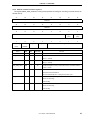
CHAPTER 1 OVERVIEW
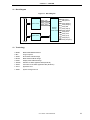
1.2 Block Diagram
Figure 1-1. Block Diagram
DDR_MCLK
DDR_MCLKB
MEMC_CLK
MEMC_CLK270
Internal system bus
System control
MEMC_RCLK
External
memory
access control
System cache
DDR_DQM[3:0]
DDR_DQS[3:0]
DDR_WEB
DDR_CKE[1:0]
DDR_CSB[1:0]
DDR_RASZ
DDR_CASZ
DDR_A[13:0]
DDR_BA[1:0]
DDR_DATA[31:0]
1.3 Terminology
MEMC:
Mobile DDR SDRAM interface
IMC:
Image composer
SHXB:
Slow master AHB-AXI bridge
MHXB:
Media master AHB-AXI bridge
DHXB:
Display master AHB-AXI bridge
ADSPD:
Data bus for ADSP application DSP (SPXK701)
ADSPI:
Instruction bus for ADSP application DSP (SPXK701)
ACPU:
Application CPU
ASMU:
System management unit
User’s Manual R19UH0028EJ0500
11
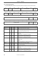
CHAPTER 2 PIN FUNCTIONS
2.1 DDR SDRAM Interface Pins
Pin Name
I/O
After Reset
DDR_MCLK
Output
32 kHz
DDR_MCLKB
Output
DDR_DQM[3:0]
Output
1111B
Write data mask
DDR_DQS[3:0]
I/O
PD (in)
Data strobe
Output
0
Write enable signal (low active)
Output
0
Clock enable signal (low active)
DDR_CSB[1:0]
Output
00
Chip select signal (low active)
DDR_RASB
Output
0
Row address strobe signal (low active)
DDR_CASB
Output
0
Column address strobe signal (low active)
DDR_A[13:0]
Output
0
Address
DDR_BA[1:0]
Output
0
Bank address
I/O
Data I/O
DDR_WEB
DDR_CKE[1:0]
Note
DDR_DATA[31:0]
Function
Clock signal output
Inverted 32 kHz Inverted clock signal output
Note To keep the DDR_CKE pin level at 0 even if the MEMC is off, the output buffer is allocated in a separate
power domain.
Remark
12
PD (in): Has a pull-down resistor (when in the input status)
User’s Manual R19UH0028EJ0500
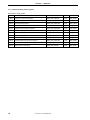
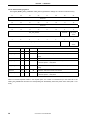
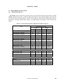
CHAPTER 3 REGISTERS
3.1 Registers
The MEMC registers allow word access only.
Do not access reserved registers. An undefined value is returned for a read access.
Do not write any value other than 0 to reserved bits in each register.
3.1.1 Request control registers and system cache setting registers
Base address: C00A_0000H
Address
Register Name
0000H
Cache/prefetch setting register
0004H
Reserved
0008H
Function disabling register
000CH-
Reserved
Register Symbol
MEMC_CACHE_MODE
MEMC_DEGFUN
R/W
After Reset
R/W
0000_0000H
R/W
0000_0000H
0010H
0014H
ACPU interrupt status register
MEMC_INTSTATUS_A
R
0000_0000H
0018H
ACPU interrupt raw status register
MEMC_INTRAWSTATUS_A
R
0000_0000H
001CH
ACPU interrupt enable set register
MEMC_INTENSET_A
R/W
0000_0000H
0020H
ACPU interrupt enable clear register
MEMC_INTENCLR_A
W
0024H
ACPU interrupt source clear register
MEMC_INTFFCLR_A
W
0028H-
Reserved
0064H
0068H
Error master ID register
MEMC_ERRMID
R
0000_0000H
006CH
Error address register
MEMC_ERRADR
R/W
0000_0000H
0070H-
Reserved
R/W
After Reset
R/W
0000_0000H
0080H
3.1.2 Memory request scheduler setting registers
Base address: C00A_0000H
Address
1000H
Register Name
Memory request scheduling mode register
Register Symbol
MEMC_REQSCH
User’s Manual R19UH0028EJ0500
13
CHAPTER 3 REGISTERS
3.1.3 External memory control registers
Base address: C00A_0000H
Address
Register Name
Register Symbol
R/W
After Reset
2000H
Memory connection setting register
MEMC_DDR_CONFIGF
R/W
0000_0808H
2004H
AC timing setting register 1
MEMC_DDR_CONFIGA1
R/W
5444_3203H
2008H
AC timing setting register 2
MEMC_DDR_CONFIGA2
R/W
00DA_0000H
200CH
Software command issuance register 1
MEMC_DDR_CONFIGC1
R/W
4040_0003H
2010H
Software command issuance register 2
MEMC_DDR_CONFIGC2
R/W
0000_03C0H
2014H
Refresh setting register 1
MEMC_DDR_CONFIGR1
R/W
7FFF_7FFFH
2018H
Refresh setting register 2
MEMC_DDR_CONFIGR2
R/W
1F5F_7C7CH
201CH
Refresh setting register 3
MEMC_DDR_CONFIGR3
R/W
0000_3F3FH
2020H
Automatic DQS timing adjustment register 1
MEMC_DDR_CONFIGT1
R/W
0000_0003H
2024H
Automatic DQS timing adjustment register 2
MEMC_DDR_CONFIGT2
R/W
0000_0000H
2028H
Automatic DQS timing adjustment register 3
MEMC_DDR_CONFIGT3
R/W
0000_0000H
202CH
Memory status check register
MEMC_DDR_STATE8
R/W
0000_0000H
14
User’s Manual R19UH0028EJ0500
CHAPTER 3 REGISTERS
3.2 Register Functions
3.2.1 Cache/prefetch setting register
This register (MEMC_CACHE_MODE: C00A_0000H) specifies whether to cache and prefetch data for each
master device.
31
30
29
28
27
26
25
24
Reserved
DIS_IMC
23
22
21
20
19
18
17
16
Reserved
DIS_SHXB
DIS_MHXB
DIS_DHXB
DIS_DSPD
DIS_DSPI
DIS_ACPU
Reserved
15
14
13
12
11
10
9
8
Reserved
PRE_IMC
7
6
5
4
3
2
1
0
Reserved
PRE_SHXB
PRE_MHXB
PRE_DHXB
PRE_DSPD
PRE_DSPI
PRE_ACPU
Reserved
Name
R/W
Bit
After Reset
Function
Reserved
R
31:25
0H
Reserved. When these bits are read, 0 is returned for each bit.
DIS_IMC
R/W
24
0B
0: Caches data read from the IMC, 1: Does not cache data
Reserved
R
23
0B
Reserved. When this bit is read, 0 is returned.
DIS_SHXB
R/W
22
0B
0: Caches data read from the SHXB, 1: Does not cache data
DIS_MHXB
R/W
21
0B
0: Caches data read from the MHXB, 1: Does not cache data
DIS_DHXB
R/W
20
0B
0: Caches data read from the DHXB, 1: Does not cache data
DIS_DSPD
R/W
19
0B
0: Caches data read from the ADSPD, 1: Does not cache data
DIS_DSPI
R/W
18
0B
0: Caches data read from the ADSPI, 1: Does not cache data
DIS_ACPU
R/W
17
0B
0: Caches data read from the ACPU, 1: Does not cache data
Reserved
R
16:9
0H
Reserved. When these bits are read, 0 is returned for each bit.
PRE_IMC
R/W
8
0B
0: Does not prefetch data while reading data from the IMC.
Reserved
R
7
0B
Reserved. When this bit is read, 0 is returned.
R/W
6
0B
0: Does not prefetch data while reading data from the SHXB.
1: Prefetches data while reading data from the IMC.
PRE_SHXB
1: Prefetches data while reading data from the SHXB.
PRE_MHXB
R/W
5
0B
0: Does not prefetch data while reading data from the MHXB.
1: Prefetches data while reading data from the MHXB.
PRE_DHXB
R/W
4
0B
0: Does not prefetch data while reading data from the DHXB.
PRE_DSPD
R/W
3
0B
0: Does not prefetch data while reading data from the ADSPD.
1: Prefetches data while reading data from the DHXB.
1: Prefetches data while reading data from the ADSPD.
PRE_DSPI
R/W
2
0B
0: Does not prefetch data while reading data from the ADSPI.
1: Prefetches data while reading data from the ADSPI.
PRE_ACPU
R/W
1
0B
0: Does not prefetch data while reading data from the ACPU.
1: Prefetches data while reading data from the ACPU.
Reserved
R
0
0B
Reserved. When this bit is read, 0 is returned.
User’s Manual R19UH0028EJ0500
15
CHAPTER 3 REGISTERS
3.2.2 Function disabling register
This register (MEMC_DEGFUN: C00A_0008H) disables some of the MEMC functions.
31
30
29
28
27
26
25
24
19
18
17
16
11
10
9
8
3
2
1
0
DISCACHE
INORDER
Reserved
23
22
21
20
Reserved
15
14
13
12
Reserved
7
6
5
4
Reserved
Name
Reserved
DISCACHE
R/W
Bit
After Reset
Function
R
31:2
0H
Reserved. When these bits are read, 0 is returned for each bit.
R/W
1
0B
Disables the system cache.
0: Enables use of the system cache.
1: Disables use of the system cache.
INORDER
R/W
0
0B
0: Issues read requests out-of-order.
1: Issues read requests in order.
16
User’s Manual R19UH0028EJ0500
CHAPTER 3 REGISTERS
3.2.3 ACPU interrupt status register
This register (MEMC_INTSTATUS_A: C00A_0014H) indicates the status of the interrupt sources for the ACPU.
31
30
29
28
27
26
25
24
19
18
17
16
11
10
9
8
3
2
1
0
ERR
SECERR
Reserved
23
22
21
20
Reserved
15
14
13
12
Reserved
7
6
5
4
Reserved
Name
R/W
Bit
After Reset
Function
Reserved
R
31:2
0H
Reserved. When these bits are read, 0 is returned for each bit.
ERR
R
1
0B
Indicates the status of error interrupts other than the security error
interrupt.
0: No interrupt source
1: There is an interrupt source.
SECERR
R
0
0B
Indicates the status of the security error interrupt.
0: No interrupt source
1: There is an interrupt source.
User’s Manual R19UH0028EJ0500
17
CHAPTER 3 REGISTERS
3.2.4 ACPU interrupt raw status register
This register (MEMC_INTRAWSTATUS_A: C00A_0018H) indicates the status of the interrupt sources for the
ACPU. The bits corresponding to the interrupt sources are set regardless of the settings of the interrupt enable set
register and the interrupt enable clear register.
31
30
29
28
27
26
25
24
19
18
17
16
11
10
9
8
3
2
1
0
RAWERR
SECRAWERR
Reserved
23
22
21
20
Reserved
15
14
13
12
Reserved
7
6
5
4
Reserved
Name
R/W
Bit
After Reset
Function
Reserved
R
31:2
0H
Reserved. When these bits are read, 0 is returned for each bit.
RAWERR
R
1
0B
Indicates the raw status of error interrupts other than the security error
interrupt.
0: No interrupt source
1: There is an interrupt source.
SECRAWERR
R
0
0B
Indicates the raw status of the security error interrupt.
0: No interrupt source
1: There is an interrupt source.
18
User’s Manual R19UH0028EJ0500
CHAPTER 3 REGISTERS
3.2.5 ACPU interrupt enable set register
This register (MEMC_INTSET_A: C00A_001CH) enables the issuance of interrupt requests for the ACPU.
Whether interrupt requests can be issued can be read from this register.
31
30
29
28
27
26
25
24
19
18
17
16
11
10
9
8
3
2
1
0
ERREN
SECERREN
Reserved
23
22
21
20
Reserved
15
14
13
12
Reserved
7
6
5
4
Reserved
Name
R/W
Bit
After Reset
Function
Reserved
R
31:2
0H
Reserved. When these bits are read, 0 is returned for each bit.
ERREN
W
1
0B
Specifies whether to enable issuance of error interrupts other than the
security error interrupt.
0: Ignored
1: Enables the interrupt.
R
Indicates whether the issuance of error interrupts other than the security
error interrupt is enabled.
0: Disabled (masked)
1: Enabled
SECERREN
W
0
0B
Specifies whether to enable issuance of the security error interrupt.
0: Ignored
1: Enables the interrupt.
R
Indicates whether the issuance of the security error interrupt is enabled.
0: Disabled (masked)
1: Enabled
User’s Manual R19UH0028EJ0500
19
CHAPTER 3 REGISTERS
3.2.6 ACPU interrupt enable clear register
This register (MEMC_INTENCLR_A: C00A_0020H) masks (disables) the issuance of interrupt requests for the
ACPU. Whether such issuance is masked can be determined by reading the MEMC_INTSET_A register.
31
30
29
28
27
26
25
24
19
18
17
16
11
10
9
8
3
2
1
0
ERRMASK
SECERRMASK
Reserved
23
22
21
20
Reserved
15
14
13
12
Reserved
7
6
5
4
Reserved
Name
R/W
Bit
After Reset
Function
Reserved
R
31:2
0H
Reserved. When these bits are read, 0 is returned for each bit.
ERRMASK
W
1
0B
Specifies whether to disable (mask) the issuance of error interrupts other
than the security error interrupt.
0: Ignored
1: Disables the sources.
When read, 0 is returned.
SECERRMASK
W
0
0B
Specifies whether to disable (mask) the issuance of the security error
interrupt.
0: Ignored
1: Disables the sources.
When read, 0 is returned.
20
User’s Manual R19UH0028EJ0500
CHAPTER 3 REGISTERS
3.2.7 ACPU interrupt source clear register
This register (MEMC_INTFFCLR_A: C00A_0024H) clears interrupt sources for the ACPU.
31
30
29
28
27
26
25
24
19
18
17
16
11
10
9
8
3
2
1
0
ERRCLR
SECERRCLR
Reserved
23
22
21
20
Reserved
15
14
13
12
Reserved
7
6
5
4
Reserved
Name
R/W
Bit
After Reset
Function
Reserved
R
31:2
0H
Reserved. When these bits are read, 0 is returned for each bit.
ERRCLR
W
1
0B
Specifies whether to clear error interrupt sources other than the security error
interrupt source.
0: Ignored
1: Clears the sources.
When read, 0 is returned.
SECERRCLR
W
0
0B
Specifies whether to clear the security error interrupt source.
0: Ignored
1: Clears the sources.
When read, 0 is returned.
User’s Manual R19UH0028EJ0500
21
CHAPTER 3 REGISTERS
3.2.8 Error master ID register
This register (MEMC_ERRMID: C00A_0068H) retains the ID of a master whose request caused an error.
31
30
29
28
27
26
25
24
19
18
17
16
11
10
9
8
3
2
1
0
Reserved
23
22
21
20
Reserved
15
14
13
12
Reserved
7
6
5
4
MID
Name
R/W
Bit
After Reset
Function
Reserved
R
31:8
0
Reserved. When these bits are read, 0 is returned for each bit.
MID
R
7:0
0
Retains the ID (master ID + AXI ID) when an error has occurred.
These bits are not overwritten by the master ID of a new error until the
current information is cleared by setting the CLEAR bit of
MEMC_ERRADR.
22
User’s Manual R19UH0028EJ0500
CHAPTER 3 REGISTERS
3.2.9 Error address register
This register (MEMC_ERRADR: C00A_006CH) retains the type of error and the address at which the error
occurred.
31
30
CLEAR
RDWT
23
22
29
28
27
26
Reserved
21
25
24
ADDR
20
19
18
17
16
11
10
9
8
3
2
1
0
ADDR
15
14
13
12
ADDR
7
6
5
4
ADDR
Name
CLEAR
ERR
R/W
Bit
After Reset
W
31
0H
Function
Specifies whether to clear the retained address.
0: Ignored.
1: Clears the address. If an error occurs after this, the new address is
retained.
R
Indicates whether a new error address can be retained.
0: A new address can be retained when an error occurs.
1: A valid address is retained, so a new address is not retained.
RDWT
R
30
0B
Indicates whether the request that caused an error was for a read or
write.
0: Read
1: Write
Reserved
R
29:28
0B
Reserved. When this bit is read, 0 is returned.
ADDR
R
27:3
0H
The value of bits 28 to 3 of the address at which a request caused an
ERR
R
2:0
000B
error is retained.
Indicates what type of error a request caused.
000B: No error
011B: An address outside the mounted range was requested.
010B: Illegal burst size (A burst size larger than 64 bits was specified.)
011B: ARBURST and AWBURST are fixed or reserved.
100B: Illegal INCR burst (INCR burst in byte or halfword units)
101b: Illegal WRAP burst
User’s Manual R19UH0028EJ0500
23
CHAPTER 3 REGISTERS
3.2.10 Memory request scheduling mode register
This register (MEMC_REQSCH: C00A_1000H) specifies the schedule of requests for memory.
31
30
29
28
27
26
25
24
19
18
17
16
11
10
9
8
Reserved
23
22
21
20
Reserved
15
14
13
12
Reserved
7
6
5
MXCASWN
Name
MXCSWN
4
MXWTWN
3
2
1
MXRDWN
0
WTDNUM
R/W
Bit
After Reset
Function
Reserved
R
31:10
0H
Reserved. When these bits are read, 0 is returned for each bit.
MXCSWN
R/W
9:8
00B
Specifies the maximum number of times the same CS can be selected in
a row.
00B: No specification, 01B: 2 times, 10B: 4 times, 11B: 6 times
MXCASWN
R/W
7:6
00B
Specifies the maximum number of times a CAS request can be selected
in a row.
00B: Once (Performs execution immediately after receiving a CAS
request), 01B: 2 times, 10B: 4 times, 11B: 6 times
MXWTWN
R/W
5:4
00B
Specifies the maximum number of times a write request can be selected
in a row for a read request during a write drain.
00B: No specification, 01B: 2 times, 10B: 4 times, 11B: 6 times
MXRDWN
R/W
3:2
00B
Specifies the maximum number of times a read request can be selected
in a row for a write request during a write drain.
00B: No specification, 01B: 2 times, 10B: 4 times, 11B: 6 times
MTDNUM
R/W
1:0
00B
Specifies the number of requests for starting a write drain.
00B: 2, 01B: 4, 10B: 6, 11B: 8
24
User’s Manual R19UH0028EJ0500
CHAPTER 3 REGISTERS
3.2.11 Memory connection setting register
This register (MEMC_DDR_CONFIGF: C00A_2000H) specifies the configuration for the external memory.
31
30
29
28
27
26
25
24
19
18
17
16
11
10
9
8
CS1_JEDEC
CS1_ENABLE
1
0
CS0_JEDEC
CS0_ENABLE
Reserved
23
22
21
20
Reserved
15
14
CS1_BANK_SPLIT
7
Reserved
CS1_BANK_SPLIT
12
Reserved
CS1_DOUBLE
5
4
Reserved
CS0_DOUBLE
6
CS0_BANK_SPLIT
Name
13
CS1_DENSITY
3
2
CS0_DENSITY
R/W
Bit
After Reset
Function
R
31:16
0H
Reserved. When these bits are read, 0 is returned for each bit.
R/W
15:14
00B
Specifies the number of banks for interleaving for CS1 (see Figure 3-1)
00B: 4-bank interleave
01B: 2-bank interleave
10B: No interleave
11B: Lower two banks interleaved, higher two banks not interleaved
Reserved
CS1_DOUBLE
R
13
0H
Reserved. When this bit is read, 0 is returned.
R/W
12
0B
Indicates whether two CS1 chips (16-bit bus chip 2) may be used.
0: Not used. (32-bit bus chip 1) 1: May be used (16-bit bus chip 2)
CS1_DENSITY
R/W
11:10
00B
Specifies the memory size of CS1.
00B: 128 Mb, 01B: 256 Mb, 10B: 512 Mb, 11B: 1 Gb
CS1_JEDEC
R/W
9
0H
0: Non-JEDEC, 1: JEDEC
CS1_ENABLE
R/W
8
0B
Specifies whether to enable access to CS1 memory.
0: Disables access, 1: Enables access
CS0_BANK_SPLIT
R/W
7:6
00B
Specifies the number of banks for interleaving for CS0 (see Figure 3-1)
00B: 4-bank interleave
01B: 2-bank interleave
10B: No interleave
11B: Lower two banks interleaved, higher two banks not interleaved
Reserved
R
5
0H
Reserved. When this bit is read, 0 is returned.
CS0_DOUBLE
R/W
4
0B
Indicates whether two CS0 chips (16-bit bus chip 2) may be used.
CS0_DENSITY
R/W
3:2
00B
0: Not used. (32-bit bus chip 1) 1: May be used (16-bit bus chip 2)
Specifies the memory size of CS0.
00B: 128 Mb, 01B: 256 Mb, 10B: 512 Mb, 11B: 1 Gb
CS0_JEDEC
R/W
1
0H
0: Non-JEDEC, 1: JEDEC
CS0_ENABLE
R/W
0
0B
Specifies whether to enable access to CS0 memory.
0: Disables access, 1: Enables access
User’s Manual R19UH0028EJ0500
25
CHAPTER 3 REGISTERS
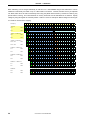
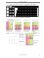
Bank addressing can be changed individually for CS0 and CS1. DDR SDRAM assigns bank addresses to column
addresses consecutively and reads out up to 4 KB of data in succession. However, because memory is separated
into banks, data cannot be read consecutively when using the partial refresh function (a function for retaining only
specific data in memory), and consecutiveness in memory areas that must be maintained is not assured. Specify
settings by using this register to avoid this problem. Table 3-1 shows an example of address assignment and Figure
3-1 shows an overview of the mapping.
CONFIG[7:0]
28
27
26
25
24
23
22
21
20
19
18
17
16
15
14
13
12
11
10
9
8
7
6
5
4
3
2
0
1
0
10
9
8
7
6
5
4
3
2
1
0
1
BA
0
0
7
CAS
6
5
4
3
2
1
0
CPU
1Gb(16)Jx2
12
0x1F
4Bank
CS
0x5F
2Bank
CS BA
1
1Gb(32)J or 512Mb(16)Jx2
11
12
10
11
10
12
11
4Bank
CS
2Bank
1
CS BA
12
0x4F
13
12
1Gb(32)N or 512Mb(16)Nx2
0x0D or 0x19
4Bank
CS
0x4D or 0x59
CS BA
1
512Mb(32)J or 256Mb(16)Jx2
7
9
RAS
8
7
6
5
6
4
3
5
2
4
3
1
2
10
11
9
10
8
7
9
RAS
8
7
6
13
11
12
10
11
9
10
10
12
11
4Bank
CS
2Bank
1
CS BA
12
0x55
13
12
10
11
5
4
6
3
5
4
2
3
1
2
0
1
1
BA
0
0
BA
9
8
7
9
RAS
8
7
6
5
4
6
5
3
4
2
0
1
0
1
BA
0
0
3
1
2
0
10
8
7
9
RAS
8
7
6
CS
0x49
2Bank
CS BA
256Mb(32)J or 128Mb(16)x2
0x11
4Bank
CS
2Bank
1
CS BA
11
0x51
12
11
0x05
4Bank
CS
0x45
2Bank
CS BA
13
11
12
10
11
9
10
9
1
10
9
10
8
9
5
4
6
5
3
4
2
3
1
12
11
9
10
8
8
7
6
5
4
3
2
1
0
6
CAS
5
4
3
2
1
0
7
7
6
5
4
3
2
1
0
6
CAS
5
4
3
2
1
0
2
8
7
9
RAS
8
7
6
5
6
4
5
3
4
2
1
1
BA
0
0
BA
8
0
1
0
1
BA
0
0
3
1
2
0
7
6
8
RAS
7
6
5
8
7
9
RAS
8
7
6
CAS
0
8
7
7
6
5
4
3
2
1
0
6
CAS
5
4
3
2
1
0
CAS
7
7
6
6
5
4
3
2
1
0
5
CAS
4
3
2
1
0
BA
4
5
3
4
2
3
1
2
0
1
1
BA
0
0
BA
8
0
1
0
1
BA
0
0
RAS
10
8
7
CAS
RAS
11
8
BA
RAS
512Mb(32)N or 256Mb(16)Nx2
0x09
4Bank
256Mb(32)N
9
8
CAS
RAS
0x15
9
BA
RAS
1
26
8
RAS
0x0F
2Bank
9
5
6
4
5
3
4
RAS
User’s Manual R19UH0028EJ0500
2
3
1
2
0
8
CAS
7
7
6
5
4
3
2
1
0
6
CAS
5
4
3
2
1
0
CAS
BA
7
7
6
6
5
4
3
2
1
0
5
CAS
4
3
2
1
0
CAS
CHAPTER 3 REGISTERS
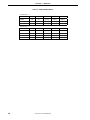
Table 3-1. Correspondence of CPU Address and External Memory Address (JEDEC)
CPU Address
Reg. setting
Memory Size Bank Interleave CS0[7:6]
A27 A26 A25 A24 A23 A22 A21 A20 A19 A18 A17 A16 A15 A14 A13 A12 A11 A10 A9
DRAM Address
CS1[15:14]
4-bank
b'00
A11 A10 A9 A8 A7 A6 A5 A4 A3 A2 A1 A0 BA1BA0A8 A7
2-bank
b'01
BA1A11 A10 A9 A8 A7 A6 A5 A4 A3 A2 A1 A0 BA0A8 A7
256 Mb 0-bank
b'10
BA1BA0A11 A10 A9 A8 A7 A6 A5 A4 A3 A2 A1 A0 A8 A7
4-bank (BA1 = L)
BA1 = L A11 A10 A9 A8 A7 A6 A5 A4 A3 A2 A1 A0 BA1BA0A8 A7
b'11
2-bank (BA1 = H
BA1 = HBA1A11 A10 A9 A8 A7 A6 A5 A4 A3 A2 A1 A0 BA0A8 A7
4-bank
b'00
A12 A11 A10 A9 A8 A7 A6 A5 A4 A3 A2 A1 A0 BA1BA0A8 A7
2-bank
b'01
BA1A12 A11 A10 A9 A8 A7 A6 A5 A4 A3 A2 A1 A0 BA0A8 A7
512 Mb 0-bank
b'10
BA1BA0A12 A11 A10 A9 A8 A7 A6 A5 A4 A3 A2 A1 A0 A8 A7
4-bank (BA1 = L)
BA1 = L A12 A11 A10 A9 A8 A7 A6 A5 A4 A3 A2 A1 A0 BA1BA0A8 A7
b'11
2-bank (BA1 = H
BA1 = HBA1A12 A11 A10 A9 A8 A7 A6 A5 A4 A3 A2 A1 A0 BA0A8 A7
4-bank
b'00
A12 A11 A10 A9 A8 A7 A6 A5 A4 A3 A2 A1 A0 BA1BA0A9 A8 A7
2-bank
b'01
BA1A12 A11 A10 A9 A8 A7 A6 A5 A4 A3 A2 A1 A0 BA0A9 A8 A7
1 Gb
0-bank
b'10
BA1BA0A12 A11 A10 A9 A8 A7 A6 A5 A4 A3 A2 A1 A0 A9 A8 A7
4-bank (BA1 = L)
BA1 = L A12 A11 A10 A9 A8 A7 A6 A5 A4 A3 A2 A1 A0 BA1BA0A9 A8 A7
b'11
2-bank (BA1 = H
BA1 = HBA1A12 A11 A10 A9 A8 A7 A6 A5 A4 A3 A2 A1 A0 BA0A9 A8 A7
A8 A7 A6 A5 A4 A3 A2 A1 A0
A6
A6
A6
A6
A6
A6
A6
A6
A6
A6
A6
A6
A6
A6
A6
A5
A5
A5
A5
A5
A5
A5
A5
A5
A5
A5
A5
A5
A5
A5
A4
A4
A4
A4
A4
A4
A4
A4
A4
A4
A4
A4
A4
A4
A4
A3
A3
A3
A3
A3
A3
A3
A3
A3
A3
A3
A3
A3
A3
A3
A2
A2
A2
A2
A2
A2
A2
A2
A2
A2
A2
A2
A2
A2
A2
A1
A1
A1
A1
A1
A1
A1
A1
A1
A1
A1
A1
A1
A1
A1
A0
A0
A0
A0
A0
A0
A0
A0
A0
A0
A0
A0
A0
A0
A0
Figure 3-1. External Memory Address Mapping
register set value
No bank division: 0x0
Dividing bank by 2: 0x1
Dividing bank by 4: 0x21
Dividing bank by 2: 0x3
partial refresh unit
COSMO partial refresh unit
Up to 4 KB units can be
accessed sequentially
Up to 2 KB units can be
accessed sequentially
Up to 1 KB units can be
accessed sequentially
The division factor of banks can be individually specified for CS0
and CS1.
1 KB units can be
accessed sequentially
Banks 0 and 1:
2 KB units can be accessed
sequentially
Banks 2 and 3:
1 KB unit can be accessed
sequentially
Dividing bank by 2: 0x3
2 KB units can be
accessed sequentially
4 KB units can be
accessed sequentially
User’s Manual R19UH0028EJ0500
No bank division: 0x0
27
CHAPTER 3 REGISTERS
Table 3-2. DDR SDRAM (JEDEC)
32-bit bus chip 1
Size
Word
Bus Width
Row
Column
BA
256 Mb
8M
32
A[11:0]
A[8:0]
BA[1:0]
512 Mb
16 M
32
A[12:0]
A[8:0]
BA[1:0]
1 Gb
32 M
32
A[12:0]
A[9:0]
BA[1:0]
Word
Bus Width
Row
Column
BA
128 Mb
8M
32
A[11:0]
A[8:0]
BA[1:0]
256 Mb
16 M
32
A[12:0]
A[8:0]
BA[1:0]
512 Mb
32 M
32
A[12:0]
A[9:0]
BA[1:0]
1 Gb
64 M
32
A[12:0]
A[10:0]
BA[1:0]
16-bit bus chip 2
Size
28
User’s Manual R19UH0028EJ0500
CHAPTER 3 REGISTERS
3.2.12 AC timing setting register 1
This register (MEMC_DDR_CONFIGA1: C00A_2004H) determines the AC timing of external memory.
31
30
29
tDCRRD
23
28
27
tRRD
22
21
20
14
19
6
5
Reserved
Name
tDCRRD
12
tRWD
7
18
16
WCL
11
10
Reserved
4
tRPD
24
17
RCL
13
Reserved
25
tRP
tRCD
15
26
9
8
tWRD
3
2
Reserved
1
0
tWPD
R/W
Bit
After Reset
Function
R
31:30
01B
Specifies the number of cycles required from a read (write) command to a read
(write) command between chips.
Specifying 0 is prohibited.
tRRD
R/W
29:27
010B
Specifies the reference clock cycles between bank activating commands.
tRP
R/W
26:24
100B
Specifies the reference clock cycles from a precharge command to a bank
activating command.
tRCD
R/W
23:20
100B
Specifies the period from a bank activating command to a read command and a
bank activating command to a write command.
0x3 at 166 MHz, 0x2 at 133 MHz, 0x1 at 100 MHz
RL = tRCD + RCL, W L = tRCD + WCL 1Note 2
RCL
R/W
19:18
01B
Specifies the read CAS latency.
00B: CL = 2, 01B: CL = 3, 10B: CL = 4, 11B: CL = 5
WCL
R/W
17:16
00B
Specifies the write CAS latency.
00B: CL = 1, 01B: CL = 2, 10B: CL = 3, 11B: CL = 4
Reserved
tRWD
R
15
0B
Reserved. When this bit is read, 0 is returned.
R/W
14:12
11B
Specifies the period from a read command to a write command.
tRWD + 4 clock cycles
Reserved
tWPD
R
11
0B
Reserved. When this bit is read, 0 is returned.
R/W
10:8
10B
Specifies the period from a write command to a read command.
tWPD + 4 clock cycles
Reserved
tRPD
R
7
0B
R/W
6:4
000B
R
3
0B
R/W
2:0
011B
Reserved. When this bit is read, 0 is returned.
Specifies the period from a read command to a precharge command.
tRPD + 4 clock cycles
Reserved
tWPD
Reserved. When this bit is read, 0 is returned.
Specifies the period from a write command to a precharge command.
tWPD + 4 clock cycles
Note tRCDR = tRCDW + 1, RL = tRCDW + RCL, WL = tRCDW + WCL 1
Because the same AC parameters are applied to CS0 and CS1, devices whose AC timing specifications
differ cannot be connected to CS0 and CS1 at the same time.
User’s Manual R19UH0028EJ0500
29
CHAPTER 3 REGISTERS
3.2.13 AC timing setting register 2
This register (MEMC_DDR_CONFIGA2: C00A_2008H) specifies the AC timing parameters for external memory
and is used to expand some functions.
31
30
29
28
Reserved
23
22
21
27
26
25
24
CS1H
CS0H
ADD_HZ
CMD_HZ
19
18
17
16
9
8
20
tSREX
15
14
tRFC
13
Reserved
7
6
IO_HZ
AutoPre
12
11
LowFrqTyp
DQS_mask_Ext
4
3
2
1
0
PstamblExt
PreamblExt
DBParkEna
Reserved
5
CLK_MODE
10
DQS_mask
DQM_HZ
(1/2)
Name
Reserved
CS1H
R/W
Bit
After Reset
Function
R
31:28
0H
Reserved. When these bits are read, 0 is returned for each bit.
R/W
27
0B
Forcibly sets CS1 to high level.
0: Active, 1: High level
CS0H
R/W
26
0B
Forcibly sets CS0 to high level.
0: Active, 1: High level
ADD_HZ
R/W
25
0B
Specifies the state of the I/O buffer for address signals.
0: Active, 1: Hi-Z
CMD_HZ
R/W
24
0B
Specifies the state of the I/O buffer for command signals.
0: Active, 1: Hi-Z
tSREX
R/W
23:20
DH
Specifies the period until returning from a self refresh.
[(tSREX + 8) 1)] clock cycles
tRFC
R/W
19:16
AH
*Note
Specifies the period until returning from an auto refresh.
tRFC + 8 clock cycles
Reserved
LowFrqTyp
R
15:13
0H
Reserved. When these bits are read, 0 is returned for each bit.
R/W
12
0B
Switches the frequency range in the low-frequency mode.
0: 30 MHz or less, 1: 30 MHz to 60 MHz
DQS_mask_Ext
R/W
11
0B
Specifies whether to delay the input DQS mask timing by 0.5 clock cycles.
0: Does not delay the timing.
1: Delays the period.
DQS_mask
R/W
10:9
00B
Specifies how much the input DQS mask timing is delayed.
00B: 2 clock cycles, 01B: 2.5 clock cycles, 10B: 3 clock cycles,
11B: Reserved
30
User’s Manual R19UH0028EJ0500
CHAPTER 3 REGISTERS
(2/2)
Name
DQM_HZ
R/W
Bit
After Reset
R/W
8
0B
Function
Specifies the state of the DQM signal for the I/O buffer.
0: Active, 1: Hi-Z
IO_HZ
R/W
7
0B
Specifies the state of the signal for the I/O buffer.
0: Active, 1: Hi-Z
AutoPre
R/W
6
1B
CLK_MODE
R/W
5:4
00B
Specifies whether to enable auto precharge.
0: Does not enable auto precharge, 1: Enables auto precharge
Specifies the timing at which read data is received.
00B: 2-clock cycle mode, 01B: 3-clock cycle mode,
10B: 1-clock cycle mode, 11B: Reserved
PstamblExt
R/W
3
0B
Specifies whether to extend the period for which the DQS postamble is
output during a write by 0.5 clock cycles.
0: Does not extend the period, 1: Extend the period
PreamblExt
R/W
2
0B
Specifies whether to extend the period for which the DQS preamble is
output during a write by 0.5 clock cycles.
0: Does not extend the period, 1: Extend the period
DBParkEna
R/W
1
0B
Specifies whether to drive DQ or DQS to low level while DDR SDRAM is in
the Hi-Z state.
0: Hi-Z control
1: Drive to low level for periods other than the period when data is valid.
Reserved
Remark
R
0
0B
Reserved. When this bit is read, 0 is returned.
Because the same AC parameters are applied to CS0 and CS1, devices whose AC timing specifications
differ cannot be connected to CS0 and CS1 at the same time.
Note
The maximum of tSREX which can be put at the time of DDR333 (166MHz) movement is 6ns (15 + 8-1)=
132 ns. SDRAM with any more min standard can't be connected.
User’s Manual R19UH0028EJ0500
31
CHAPTER 3 REGISTERS
3.2.14 Software command issuance register 1
This register (MEMC_DDR_CONFIGC1: C00A_200CH) specifies addresses and data when the extended mode
register is set up for external memory.
31
30
29
28
27
26
25
24
18
17
16
10
9
8
2
1
0
MODREG_EMRS
23
22
21
20
19
MODREG_EMRS
15
14
13
12
11
MODREG_MRS
7
6
5
4
3
MODREG_MRS
Name
R/W
Bit
After Reset
MODREG_EMRS
R/W
31:16
4040H
Function
Specifies mode register setting command issuance address 2
(DDR SDRAM: BA1, BA0, A[13:0])
MODREG_MRS
R/W
15:0
0003H
Specifies mode register setting command issuance address 1
(DDR SDRAM: BA1, BA0, A[13:0])
A command that sets up an extended mode register is issued for external memory based on the address specified
for the MODREG_EMRS bit.
A command that sets up an extended mode register is issued for external memory based on the address specified
for the MODREG_MRS bit. The address is fixed to 0xFF FFF0.
When setting up a mode register and issuing the Initialize, MRS, or EMRS command, set up this register as follows:
Initialize command
MODREG_EMRS = {2’b10, EMRS setting}, MODREG_MRS = {2’b00, MRS setting}
MRS command
MODREG_EMRS = {2’b00, MRS setting}, MODREG_MRS = {2’b00, any value}
EMRS command
MODREG_EMRS = {2’b10, EMRS setting}, MODREG_MRS = {2’b00, any value}
When issuing precharge commands, set up this register as follows:
All bank precharge
MODREG_MRS[10] = 1’b1
Bank precharge
MODREG_MRS[15:14] = Target bank address, MODREG_MRS[10] = 1’b0
Restriction and caution on command issuance:
Requests to issue commands are ignored when the CMD_STATE bit of the MEMC_DDR_CONFIGC2
register is set to 0 (busy).
32
User’s Manual R19UH0028EJ0500
CHAPTER 3 REGISTERS
3.2.15 Software command issuance register 2
This register (MEMC_DDR_CONFIGC2: C00A_2010H) specifies the settings for controlling command issuance for
external memory.
31
30
29
28
27
26
25
24
19
18
17
16
11
10
9
8
CMD_STATE
CMD_STATE
(CS1)
(CS0)
1
0
Reserved
23
22
21
20
Reserved
15
14
13
12
Reserved
7
6
5
CMD_REQ_
CMD_
LOCK
ENABLE
4
3
CS1_TARGET CS0_TARGET
2
CMD_SET
(1/2)
Name
R/W
Bit
After Reset
Function
Reserved
R
31:10
0H
Reserved. When these bits are read, 0 is returned for each bit.
CMD_STATE(CS1)
R
9
1B
Indicates the execution status of a command requested by CS.
0: Busy, 1: Standby
CMD_STATE(CS0)
R
8
1B
Indicates the execution status of a command requested by CS.
0: Busy, 1: Standby
CMD_REQ_LOCK
R/W
7
1B
Specifies the signal to lock any request other than for command issuance.
0: Lock, 1: Unlock
CMD_ENABLE
R/W
6
1B
Specifies whether to issue a command request.
0: Requests command issuance.
This bit is automatically set to 1 during the next clock cycle.
CS1_TARGET
R/W
5
0B
Sets the command request flag for CS1.
0: Does not set the flag.
1: Sets the flag.
CS0_TARGET
R/W
4
0B
Sets the command request flag for CS0.
0: Does not set the flag.
1: Sets the flag.
User’s Manual R19UH0028EJ0500
33
CHAPTER 3 REGISTERS
(2/2)
Name
CMD_SET
R/W
Bit
After Reset
R/W
3:0
0H
Function
Specifies the control command.
0111B: Disables the CKE signal.
1000B: Executes the DDR SDRAM initialization sequence.
1001B: Precharges all banks.
1010B: Executes a CBR refresh.
1011B: Shifts to the self refresh mode.
1100B: Shifts to the deep power down mode.
1101B: Enables the CKE signal.
1110B: Reads from the (extended) mode register.
1111B: Writes to the (extended) mode register.
The command specified by the CMD_SET bit can be issued if a command code is specified for the target memory
at the same time as the CMD_ENABLE bit is set to 0 in this register.
The memory assigned to CS0 and CS1 can be specified as target memory at the same time.
Before setting the CMD_ENABLE bit, make sure that the CMD_STATE bit is set to 1.
No command requests are accepted if the CMD_STATE bit is set to 0 (busy) upon command issuance. After a
command request is issued while the CMD_REQ_LOCK bit is set to 0 (locked), only requests for software commands
are accepted.
When the deep power down mode is entered, cancel the auto self refresh and CBR refresh for the target CS.
34
User’s Manual R19UH0028EJ0500
CHAPTER 3 REGISTERS
3.2.16 Refresh setting register 1
This register (MEMC_DDR_CONFIGR1: C00A_2014H) individually specifies refresh cycles in external memory for
CS0 and CS1.
31
30
29
CS1_REF_
28
27
CS1_REF_STOCK
CS1_CBR_
OVER
23
26
25
24
CS1_REF_COUNT
SREF
22
21
20
19
18
17
16
10
9
8
CS1_REF_COUNT
15
14
13
CS0_REF_
12
11
CS0_REF_STOCK
CS0_CBR_
OVER
7
CS0_REF_COUNT
SREF
6
5
4
3
2
1
0
CS0_REF_COUNT
Name
CS1_REF_OVER
R/W
Bit
After Reset
Function
R
31
0B
Indicates whether the number of times refreshes for CS1 still needs to be
executed exceeds the maximum.
CS1_REF_STOCK
R
30:28
7H
Indicates the number of times refreshes for CS1 still needs to be
executed.
CS1_CBR_SREF
R/W
27
1B
Specifies whether to forcibly execute a CBR refresh at least once when
CS1 is in the self refresh mode.
CS1_REF_COUNT
R/W
26:16
7FFH
Specifies the CS1 refresh timer counter value.
Refresh cycle = RCLK (refresh counter clock) cycles specified value
CS0_REF_OVER
R
15
0B
Indicates whether the number of times refreshes for CS0 still needs to be
executed exceeds the maximum.
CS0_REF_STOCK
R
14:12
7H
Indicates the number of times refreshes for CS0 still needs to be
executed
CS0_CBR_SREF
R/W
11
1B
Specifies whether to forcibly execute a CBR refresh at least once when
CS0 is in the self refresh mode.
CS0_REF_COUNT
R/W
10:0
7FFH
Specifies the CS0 refresh timer count value.
Refresh cycle = RCLK (refresh counter clock) cycles specified value
The refresh counter is incremented during each refresh cycle by the REF_STOCK counter. A refresh is executed
when the self refresh mode is entered or when the refresh counter reaches the threshold.
User’s Manual R19UH0028EJ0500
35
CHAPTER 3 REGISTERS
3.2.17 Refresh setting register 2
This register (MEMC_DDR_CONFIGR2: C00A_2018H) specifies the settings for a refresh in external memory.
31
30
29
Reserved
STOCK_
28
27
CS1_STOCK_DRAIN
26
25
CS1_STOCK_MAX
24
CS1_TIMER
DRAIN_TYP
23
_RST
22
Reserved
21
COUNT_
20
19
CS0_STOCK_DRAIN
18
17
CS0_STOCK_MAX
16
CS0_TIMER
COMMON
15
_RST
14
13
12
11
10
CS1_SREF_COUNT
7
6
5
4
3
9
8
CS1_SREF_
CS1_REF_
AUTO
AUTO
1
0
CS0_SREF_
CS0_REF_
AUTO
AUTO
2
CS0_SREF_COUNT
(1/2)
Name
Reserved
STOCK_DRAIN_TYP
R/W
Bit
After Reset
Function
R
31
0B
Reserved. When this bit is read, 0 is returned.
R/W
30
0B
Specifies whether to decrement the refresh counter (whether to execute CBR)
when no read request is being received and the number of write requests is
the write buffer drain threshold value or lower.
CS1_STOCK_DRAIN
R/W
29:28
01B
Specifies how many times a refresh is executed before CS1 enters the self
refresh mode.
Specifiable range: 1 to 3 (Specifying 0 is prohibited.)
CS1_STOCK_MAX
R/W
27:25
7H
Specifies the maximum number of refreshes for CS1.
Specifiable range: 1 to 7 (Specifying 0 is prohibited.)
CS1_TIMER_RST
R/W
24
1B
Specifies whether to reset CS1_REF_COUNT, CS1_REF_STOCK, and
CS1_REF_OVER.
0: Reset
This bit is automatically set to 1 during the next clock cycle.
Reserved
COUNT_COMMON
R
23
0B
Reserved. When this bit is read, 0 is returned.
R/W
22
1B
Specifies whether to apply the auto refresh cycle for CS0 to CS1.
(The counter for CS1 stops.)
CS0_STOCK_DRAIN
R/W
21:20
01B
Specifies how many times a refresh is executed before CS0 enters the self
refresh mode.
Specifiable range: 1 to 3 (Specifying 0 is prohibited.)
CS0_STOCK_MAX
R/W
19:17
7H
Specifies the maximum number of refreshes for CS0.
Specifiable range: 1 to 7 (Specifying 0 is prohibited.)
36
User’s Manual R19UH0028EJ0500
CHAPTER 3 REGISTERS
(2/2)
Name
CS0_TIMER_RST
R/W
Bit
After Reset
R/W
16
1B
Function
Specifies whether to reset CS0_REF_COUNT, CS0_REF_STOCK, and
CS0_REF_OVER.
0: Reset
This bit is automatically set to 1 during the next clock cycle.
CS1_SREF_COUNT
R/W
15:10
1FH
Specifies CS1 self refresh counter values.
Auto self refresh entry idle counter set value multiplied by 16.
CS1_SREF_AUTO
R/W
9
0B
Specifies whether to enable issuance of CS1 auto self refresh requests
(SREF).
0: Disable, 1: Enable
CS1_REF_AUTO
R/W
8
0B
Specifies whether to enable issuance of CS1 auto refresh requests (CBR).
0: Disable, 1: Enable
CS0_SREF_COUNT
R/W
7:2
1FH
Specifies CS0 self refresh counter values.
Auto self refresh entry idle counter set value multiplied by 16.
CS0_SREF_AUTO
R/W
1
0B
Specifies whether to enable issuance of CS0 auto self refresh requests
(SREF).
0: Disable, 1: Enable
CS0_REF_AUTO
R/W
0
0B
Specifies whether to enable issuance of CS0 auto refresh requests (CBR).
0: Disable, 1: Enable
The refresh counter is incremented during each refresh cycle by the REF_STOCK counter. A refresh is executed
when the self refresh mode is entered or when the refresh counter reaches the threshold. When the REF_STOCK
counter exceeds the maximum value, the CS0/1_REF_OVER bits of the MEMC_DDR_CONFIGR1 register are set to
1.
User’s Manual R19UH0028EJ0500
37
CHAPTER 3 REGISTERS
3.2.18 Refresh setting register 3
This register (MEMC_DDR_CONFIGR3: C00A_201CH) specifies the settings for a refresh in external memory.
31
30
29
28
27
26
25
24
19
18
17
16
11
10
9
8
Reserved
CS1_APD_
Reserved
23
22
21
20
Reserved
15
14
13
12
CS1_APD_COUNT
AUTO
7
6
5
4
3
2
CS0_APD_COUNT
1
0
Reserved
CS0_APD_
AUTO
Name
Reserved
CS1_APD_COUNT
R/W
Bit
After Reset
Function
R
31:16
0H
R/W
15:10
3FH
R
9
0B
Reserved. When this bit is read, 0 is returned.
R/W
8
0B
Specifies whether to request an automatic CS1 power down.
Reserved. When these bits are read, 0 is returned for each bit.
Specifies the automatic CS1 power down counter value (the idle counter
value).
Reserved
CS1_APD_AUTO
0: Normal operation, 1: Requested
CS0_APD_COUNT
R/W
7:2
3FH
Specifies the automatic CS0 power down counter value (the idle counter
value).
Reserved
CS0_APD_AUTO
R
1
0B
R/W
0
0b
Reserved. When this bit is read, 0 is returned.
Specifies whether to request an automatic CS0 power down.
0: Normal operation, 1: Requested
When no received requests remain in the request queue, the counter is incremented up to the value set to the
CS0/1_APD_COUNT bits and then the corresponding CS automatically enters the power down mode (CKE = low
level).
38
User’s Manual R19UH0028EJ0500
CHAPTER 3 REGISTERS
3.2.19 Automatic DQS timing adjustment register 1
This register (MEMC_DDR_CONFIGT1: C00A_2020H) specifies the adjustment of delays in external memory.
31
30
29
28
27
26
Reserved
23
22
21
20
19
13
12
5
4
Reserved
CLK270_DELAY
Reserved
DQS_O_DELAY
Reserved
CALIBRATE_PAT
9
8
2
1
0
CALIBRATE
CALIBRATE
AUTO_CALI
_PAT
_STATE
BRATE
10
3
Reserved
MCLK_DELAY
16
DQS_O_DELAY
6
Reserved
17
11
Reserved
Name
18
CLK270_DELAY
14
7
24
MCLK_DELAY
Reserved
15
25
R/W
Bit
After Reset
Function
R
31:28
0H
Reserved. When these bits are read, 0 is returned for each bit.
R/W
27:24
0H
Adjusts the MCLK delay (delay 1).
R
23:21
0H
Reserved. When these bits are read, 0 is returned for each bit.
R/W
20:16
0H
Adjusts the CLK270 delay (delay 4).
R
15:12
0H
Reserved. When these bits are read, 0 is returned for each bit.
R/W
11:8
0H
Adjusts the delay of DQS output (delay 3).
R
7:3
0H
Reserved. When these bits are read, 0 is returned for each bit.
R/W
2
0B
Specifies the calibration pattern.
0: 0xFFFF 0x0000, 1: 0xAAAA 0x5555
CALIBRATE_STATE
R/W
1
1B
Indicates the calibration status.
0: Busy, 1: Ready
AUTO_CALIBRATE
R/W
0
1B
Specifies the start of automatic calibration.
0: Calibration starts.
Delays can be added to each signal line by setting up this register.
The optimum delay values obtained by calibration are stored in the MEMC_DDR_CONFIGT3 register.
When the delay is adjusted using this register, set the MEMCCLK270_SEL bit of the MEMCCLK270_SEL register to 1
in the ASMU.
User’s Manual R19UH0028EJ0500
39
CHAPTER 3 REGISTERS
3.2.20 Automatic DQS timing adjustment register 2
This register (MEMC_DDR_CONFIGT2: C00A_2024H) specifies the automatic adjustment of delays in external
memory.
31
30
29
28
Reserved
23
21
20
Reserved
13
12
Reserved
5
4
Reserved
Reserved
DQS0_DELAY
Reserved
DQS1_DELAY
Reserved
DQS2_DELAY
Reserved
DQS3_DELAY
19
11
3
18
17
16
10
9
8
2
1
0
DQS3_DELAY
R/W
Bit
After Reset
Function
R
31:30
0H
Reserved. When these bits are read, 0 is returned for each bit.
R/W
29:24
0H
Optimizes the DQS0 delay.
R
23:22
0H
Reserved. When these bits are read, 0 is returned for each bit.
R/W
21:16
0H
Optimizes the DQS1 delay.
R
15:14
0H
Reserved. When these bits are read, 0 is returned for each bit.
R/W
13:8
0H
Optimizes the DQS2 delay.
R
7:6
0H
Reserved. When these bits are read, 0 is returned for each bit.
R/W
5:0
0H
Optimizes the DQS3 delay.
Delays can be added to each input DQS signal line by setting up this register.
40
24
DQS2_DELAY
6
Name
25
DQS1_DELAY
14
7
26
DQS0_DELAY
22
15
27
User’s Manual R19UH0028EJ0500
CHAPTER 3 REGISTERS
3.2.21 Automatic DQS timing adjustment register 3
This register (MEMC_DDR_CONFIGT3: C00A_2028H) stores the result of adjustment for automatic calibration
delays.
31
30
29
28
Reserved
23
21
20
Reserved
13
12
Reserved
24
19
18
17
16
11
10
9
8
1
0
DQS2_DELAY_VAL
6
5
4
Reserved
Name
25
DQS1_DELAY_VAL
14
7
26
DQS0_DELAY_VAL
22
15
27
3
2
DQS3_DELAY_VAL
R/W
Bit
After Reset
Function
Reserved
R
31:30
0H
Reserved. When these bits are read, 0 is returned for each bit.
DQS0_DELAY_VAL
R
29:24
0H
Stores the result of adjusting the DQS0 delay.
Reserved
R
23:22
0H
Reserved. When these bits are read, 0 is returned for each bit.
DQS1_DELAY_VAL
R
21:16
0H
Stores the result of adjusting the DQS1 delay.
Reserved
R
15:14
0H
Reserved. When these bits are read, 0 is returned for each bit.
DQS2_DELAY_VAL
R
13:8
0H
Stores the result of adjusting the DQS2 delay.
Reserved
R
7:6
0H
Reserved. When these bits are read, 0 is returned for each bit.
DQS3_DELAY_VAL
R
5:0
0H
Stores the result of adjusting the DQS3 delay.
The optimum delay values obtained by calibration are stored in the DQS0_DELAY_VAL to DQS3_DELAY_VAL bits.
When adjustment for automatic calibration is executed, set the MEMCCLK270_SEL bit of the MEMCCLK270_SEL
register to 1 in the ASMU.
User’s Manual R19UH0028EJ0500
41
CHAPTER 3 REGISTERS
3.2.22 Memory status check register
This register (MEMC_DDR_STATE8: C00A_202CH) is used to monitor the status of CS0 and CS1.
31
30
29
28
27
26
25
24
19
18
17
16
11
10
9
8
3
2
1
0
CS1_STATE
23
22
21
20
CS1_STATE
15
14
13
12
CS0_STATE
7
6
5
4
CS0_STATE
Name
CS1_STATE
R/W
Bit
After Reset
R
31:16
0H
Function
Indicates the status of the memory connected to CS1.
0x0: Idle
0x1: Extended mode register setting
0x3: Self refresh
0x5: Auto power down
0x6: Self refresh end
0x7: Deep power down
0x8: Bank precharge/all bank precharge
0xA: Read/write
0xC: Forced CBR refresh
0xE: CBR refresh
0xF: Mode register setting
CS0_STATE
R
15:0
0H
Indicates the status of the memory connected to CS0.
0x0: Idle
0x1: Extended mode register setting
0x3: Self refresh
0x5: Auto power down
0x6: Self refresh end
0x7: Deep power down
0x8: Bank precharge/all bank precharge
0xA: Read/write
0xC: Forced CBR refresh
0xE: CBR refresh
0xF: Mode register setting
42
User’s Manual R19UH0028EJ0500
CHAPTER 4 USAGE
4.1 External Memory Access Control
4.1.1
External Memory Access
DDR SDRAM can be connected as an external memory and can be read and written in 8-burst length. The DDR
SDRAM is divided into four banks. Consecutive reading access within a 1-KB consecutive address in the same bank
(CAS access) can be performed efficiently. However, access outside the 1-KB consecutive address (RAS access) is
less efficient. Accessing a different bank is efficient. The DDR scheduler sorts requests in order to make access
efficient.
Table 4-1. Clock Counts Required for 16-Word Access (Burst Length = 8)
Mode
Number of DDR CLK Cycles
133 MHz
166 MHz
Auto
Non-auto
Auto
Non-auto
Other bank (read read)
15
15
15
15
Same bank (read read CAS)
22
15
22
15
Same bank (read read RAS)
22
22
22
22
Other bank (read write)
21
21
21
21
Same bank (read write CAS)
25
21
25
21
Same bank (read write RAS)
25
25
25
25
Other bank (write read)
17
17
17
17
Same bank (write read CAS)
25
17
25
17
Same bank (write read RAS)
25
25
25
25
Other bank (write write)
18
18
18
18
Same bank (write write CAS)
28
18
28
18
Same bank (write write RAS)
28
28
28
28
Other chip (read read)
16
16
16
16
Other chip (read write)
21
21
21
21
Other chip (write read)
20
20
20
20
Other chip (write write)
18
18
18
18
Power on
88
88
81
81
Self refresh recovery
16
16
20
20
Auto refresh recovery
15
15
18
18
Deep power down recovery
84
84
77
77
User’s Manual R19UH0028EJ0500
43
CHAPTER 4 USAGE
4.1.2
External Memory Access
The DDR module is controlled by two clock signals, MEMC_CLK and MEMC_CLK270, which are supplied by the
ASMU (system management unit). The frequency of MEMC_CLK is 133 or 166 MHz. MEMC_CLK270 is obtained by
shifting the phase of MEMC_CLK by 270.
If there are no read/write requests in the request queue, DDR SDRAM
enters the self refresh mode, in which no clock requests are issued. When a read or write request is queued, the
MEMC requests the issuance of a clock signal to the ASMU.
In normal mode, the maximum frequency of MEMC_CLK is 166 MHz and 133 MHz. When MEMC_CLK operating
frequency is switched, a handshake with the ASMU occurs. Figure 4-1 shows the frequency switch timing. The AC
parameters for the timing of exiting a refresh and starting an auto refresh are optimized according to the switched
operating frequency.
When the operating clock is switched to the system clock generated by PLL3, the frequency is judged to be low by
receiving the MEMC_CLK operating frequency recognition signal sent from the ASMU, and the AC parameters for
DDR SDRAM are adjusted to the low frequency mode.
The clock frequency is switched immediately if all chips have entered the self refresh mode when clock frequency
switching is requested. (ACK is returned immediately.) When a request is being processed (DDR SDRAM is being
accessed), the clock frequency is switched after the requested action is executed. (ACK is returned after execution.)
When a CBR refresh request is received, a CBR refresh is executed after the clock frequency is switched. When a
clock frequency switch request is received while the MEMC is exiting the self refresh mode, the clock frequency is
switched immediately after the self refresh mode is exited.
44
User’s Manual R19UH0028EJ0500
CHAPTER 4 USAGE
Figure 4-1. Timing at Which MEMC_CLK Operating Frequency Is Switched
Sequence for changing the clock frequency from high to low
T0
T1
T2
T3
T4
T5
T6
T7
T8
T9
T10
T11
T12
T11
T12
MEMC_CLK
(DDR module clock)
ASMU_CLKCH_REQ
(Switch request signal from ASMU)
DDR_CLKCH_ACK
(Switch enable signal from
DDR module)
33 MHz or 66 MHz
ASMU_CLKFRQ
Normal mode
ASMU_CLKFRQA
(Normal/Half/Quarter recognition signal)
Half mode
CKE
CLK_REQ
Level before switching is maintained.
If low, DDR SDRAM is in self-refresh mode
(several hundred ns)
Sequence for changing the clock frequency from low to high
T0
T1
T2
T3
T4
T5
T6
T7
T8
T9
T10
MEMC_CLK
(DDR module clock)
ASMU_CLKCH_REQ
DDR_CLKCH_ACK
ASMU_CLKFRQ
Low frequency
133 MHz or 166 MHz
ASMU_CLKFRQA
Quarter mode
Normal mode
CKE
CLK_REQ
At least 1 s is required in quarter mode
Level before switching is maintained.
(At least 800 s is required when the
main PLL is activated)
4.1.3 Clock Phase Control
Addresses and commands are issued when MEMC_CLK is shifted by 180. In read cycles, data is received
(latched) based on the DQS signal output from external memory, with delays added. In write cycles, data is output in
synchronization with MEMC_CLK270.
Figure 4-2. Clock adjustment mechanism
User’s Manual R19UH0028EJ0500
45
CHAPTER 4 USAGE
MEMC Conposision (Clock adjustment mechanism)
MCLK_DELAY
MCLK_DELAY
CLK
Delay
CLK_DELAY_270
CLK_270
Delay
CLK_DELAY_270
IO
DQS_O_DELAY
Delay
IO
DQS_O_DELAY
ASMU
AXI
A/制御
DATA_O/
DQM
IO
DQS_O
IO
MCLK/
MCLKB
LPDDR
A/制御
DATA/
DQM
DQS
DATA_I
Delay
LOGIC
MEMCIO
MEMC
DQS[3:0]_DELAY
Figure 4-3. Write phase adjustment
WRITE adjustment
MCLK
MCLKB
Output MCLK is
adjusted by changing
MCLK_DELAY
DQS
DATA
DQM
The phase of DQS is
adjusted most suitably by
changing DQS_DELAY.
The phase of DQ/DQS is
adjusted by changing
CLK_DELAY_270.
Figure 4-4. Read phase adjustment
46
User’s Manual R19UH0028EJ0500
CHAPTER 4 USAGE
READ adjustment
The phase of most suitable DQS
which calculates the most
suitable DQS[0123]_DELAY
value in calibration S/W and
latches READ DATA by EM1,
calculation/adjustment.
DQS
DATA
(fastest)
DATA
(slowest)
(DATA Window)
User’s Manual R19UH0028EJ0500
47
CHAPTER 4 USAGE
4.1.4 Arbitration
The DDR module arbitrates the following three instructions:
<1> Access instructions from the request queue (independent of read/write)
<2> Self refresh instructions from the IDLE/REF counter, or auto refresh instructions (2 types)
<3> Software command instructions (7 types)
The MEMC outputs the control signals for arbitration according to the priority shown in the following table.
Table 4-2. DDR Module Priority in Processing
48
<1>
<2>
<3>
Access
Self/Auto Refresh
Software command
2
3
Self refresh
1
3
2
Auto refresh
1
1
2
Self refresh
3
2
1
Auto refresh
3
2
3
Self refresh
1
3
1
Auto refresh
2
1
2
Self refresh
3
2
1
Auto refresh
3
1
2
Self refresh
3
2
1
Auto refresh
3
2
3
Self refresh
1
3
1
Auto refresh
2
2
3
Self refresh
1
3
1
Auto refresh
2
User’s Manual R19UH0028EJ0500
Initialize
Precharge all
Auto refresh
Self refresh
Deep power down
Read mode register
Write mode register
CHAPTER 4 USAGE
4.1.5 Refresh control
To retain data, the MEMC refreshes DDR SDRAM at a constant interval. The self refresh mode is entered when no
read or write request is being received after setting the CS0/1_REF_AUTO bits or CS0/1SREF_AUTO bits of the
MEMC_DDR_CONFIGR2 register. In other cases, the number of refreshes that has been executed is counted during
each refresh cycle, and CBR refreshes are performed for the relevant number of times at a specific timing. For the
catalogue value of DDR SDRAM whose row address is allocated in 16 M-word units, refreshes must be executed at
least 8,192 times per 64 ms (once in 7 to 8 s).
In EM1, the refresh cycle can be specified freely for the CS0/1_REF_COUNT bits of the MEMC_DDR_CONFIGR2
register. When operation enters a refresh cycle, the number of times refreshes still need to be executed is stored in
the CS0/1_REF_STOCK bits of the MEMC_DDR_CONFIGR1 register. When this number reaches the specified
value (the values of the CS0/1_STOCK_MAX bits of the MEMC_DDR_CONFIGR2 register), acceptance of requests
from the request queue is forcibly suspended temporarily and a CBR refresh is executed once at the top priority.
While in the self refresh mode, the timer that counts the refresh cycles stops temporarily and resumes when the mode
is exited.
If refreshes still need to be executed when the self refresh mode is entered, CBR refreshes are executed multiple
times (up to the value specified by the CS0/1_STOCK_DRAIN bits of the MEMC_DDR_CONFIGR2 register) before a
self refresh is executed. Figure 4-5 shows the processing from when shifting to CBR refresh execution and after
shifting to the self refresh mode. Refresh operation is controlled individually for CS0 and CS1.
Figure 4-5. Refresh Control Status Transitions
IDLE
IDLE
CS0_SREF_AUTO = 0
CS0_REF_AUTO = 0
CS0_SREF_AUTO = 1
CS0_REF
_AUTO = 0
CS0_REF_AUTO = 1
IDLE
Counter
ACT
Refresh
Counter
ACT
CS0_MODE_SREF = 0
Refresh
Counter
Suspend
CS0_MODE_SREF = 1
(Resume)
(CS0_SREF_COUNT_VAL = CS0_SREF_COUNT) &&
(CS0_REF_STOCK = 0)
SREF
IDLE
FIF_AVALID
=1
CBR1
CBR2
N times
User’s Manual R19UH0028EJ0500
49
CHAPTER 4 USAGE
4.1.6 Software command control
By using the MEMC_DDR_CONFIGC2 register, DDR SDRAM commands listed in Table 4-2 can be issued and
refresh can be controlled.
When setting a (extended) mode register of DDR SDRAM:
Set the address of the command to be issued to DDR SDRAM by using the MEMC_DDR_CONFIGC1 register.
Set the CMD_SET bit of the MEMC_DDR_CONFIGC2 register to 1111B (to write the mode register).
Set the CMD_ENABLE bit to 0 at the same time; the command is then issued.
When issuing a precharge command
Set the target bank by using the MEMC_DDR_COFIGC1 register.
To precharge all banks, set
MODEREG_MRS[10] to 1. To precharge selected banks, set MODEREG_MRS[10] to 0 and set the target
bank address by using MODEREG_MRS[15:14].
Set the CMD_SET bit of the MEMC_DDR_CONFIGC2 register to 1001B (to precharge banks).
Set the CMD_ENABLE bit to 0 at the same time; the command is then issued.
When issuing other commands
Setting MEMC_DDR_CONFIG1 is unnecessary.
Set the corresponding command by using the CMD_SET bit of the MEMC_DDR_CONFIGC2 register.
Set the CMD_ENABLE bit to 0 at the same time; the command is then issued.
Remark
Commands are issued after processing of all requests. If the CMD_REQ_LOCK bit has been set when
a command is issued, the subsequent requests other than those request for command issuance are
held pending until the request lock is released with the CMD_REQ_LOCK bit. Whether a command has
been executed can be checked with the CMD_STATE bit. When a software command is executed while
the CMD_STATE bit is set to 0 (busy), the command is ignored. When a command to request that the
CKE signal be enabled is issued, a clock request is issued at the same time.
Table 4-3. Software Commands
Command
Function
Processing
Initial Seq Auto Exec
Executes initial sequence at power-on.
PALL CBR CBR MRS EMRS
Precharge
Executes precharge.
A10 = H for PALL, A10 = L and BA[10] = 11B for PRE
Auto refresh
Executes auto refresh.
Issues a CBR command.
Self refresh
Executes self refresh command.
Issues an SREF command.
Deep power down
Executed deep power down.
Issues a DPD command.
Enabling CKE
CKE pin control
Enables controlling the CKE signal by the MEMC.
Disabling CKE
CKE pin control
Disables controlling the CKE signal by the MEMC.
Read mode register
Read from mode register
Write mode register
Write to mode register
50
Issues an MRS/EMRS command.
User’s Manual R19UH0028EJ0500
CHAPTER 4 USAGE
4.1.7 Power on/off sequence
When the power is initially turned on, the DDR_RST signal is asserted after a clock signal is supplied. (This signal
is controlled by the ASMU.) Immediately after a reset, first set up DDR registers such as MEMC_DDR_CONFIGF,
MEMC_DDR_CONFIGFA1, and MEMC_DDR_CONFIGA2.
Next, individually execute the initialization sequence
listed in the table below for CS0 and CS1 by using software commands. The sequence might differ depending on the
connected DDR SDRAM. For details, see documents such as the data sheet for the device.
For safety, it is recommended to set the CMD_REQ_LOCK bit of the MEMC_DDR_CONFIGC2 register to 1 to lock
any requests other than the command issuance. When issuing the last command, set the CMD_REQ_LOCK bit to 0
to release the locked state.
Figure 4-6. DDR SDRAM Power On Timing
Power on sequence for DDR SDRAM
T0
T1
T2
T3
T4
T5
T6
T7
T8
T9
T10
T11
T12
MEMC_CLK
(DDR module clock)
DDR_RST
Software command issued
CMD_ENABLE
Software command issued
Initial sequence processing
External CKE/CE2 pin
(SDRAM/COSMO)
External CS/CE1 pin
Power down processing is always CS0,1, automatic power down request, the automatic self-refresh and the
automatic refreshment request Disable. All Bank Precharge request-> issue confirmation-> CKE
Enable issue
request-> Issue confirmation-> Deep power down issue (CMD_REQ_LOCK = 1)-> Issue confirmation-> Do by an
order of the end..
User’s Manual R19UH0028EJ0500
51
Revision History
52
Date
Revision
Comments
February 10, 2009
1.0
−
April 27, 2009
2.0
Incremental update from comments to the 1.0.
June 12, 2009
3.0
Incremental update from comments to the 2.0.
September 30, 2009
4.0
Incremental update from comments to the 3.0.
June 30, 2010
5.0
Incremental update from comments to the 4.0.
User’s Manual R19UH0028EJ0500
http://www.renesas.com
SALES OFFICES
Refer to "http://www.renesas.com/" for the latest and detailed information.
Renesas Electronics America Inc.
2880 Scott Boulevard Santa Clara, CA 95050-2554, U.S.A.
Tel: +1-408-588-6000, Fax: +1-408-588-6130
Renesas Electronics Canada Limited
1101 Nicholson Road, Newmarket, Ontario L3Y 9C3, Canada
Tel: +1-905-898-5441, Fax: +1-905-898-3220
Renesas Electronics Europe Limited
Dukes Meadow, Millboard Road, Bourne End, Buckinghamshire, SL8 5FH, U.K
Tel: +44-1628-585-100, Fax: +44-1628-585-900
Renesas Electronics Europe GmbH
Arcadiastrasse 10, 40472 Düsseldorf, Germany
Tel: +49-211-65030, Fax: +49-211-6503-1327
Renesas Electronics (China) Co., Ltd.
7th Floor, Quantum Plaza, No.27 ZhiChunLu Haidian District, Beijing 100083, P.R.China
Tel: +86-10-8235-1155, Fax: +86-10-8235-7679
Renesas Electronics (Shanghai) Co., Ltd.
Unit 204, 205, AZIA Center, No.1233 Lujiazui Ring Rd., Pudong District, Shanghai 200120, China
Tel: +86-21-5877-1818, Fax: +86-21-6887-7858 / -7898
Renesas Electronics Hong Kong Limited
Unit 1601-1613, 16/F., Tower 2, Grand Century Place, 193 Prince Edward Road West, Mongkok, Kowloon, Hong Kong
Tel: +852-2886-9318, Fax: +852 2886-9022/9044
Renesas Electronics Taiwan Co., Ltd.
7F, No. 363 Fu Shing North Road Taipei, Taiwan
Tel: +886-2-8175-9600, Fax: +886 2-8175-9670
Renesas Electronics Singapore Pte. Ltd.
1 harbourFront Avenue, #06-10, keppel Bay Tower, Singapore 098632
Tel: +65-6213-0200, Fax: +65-6278-8001
Renesas Electronics Malaysia Sdn.Bhd.
Unit 906, Block B, Menara Amcorp, Amcorp Trade Centre, No. 18, Jln Persiaran Barat, 46050 Petaling Jaya, Selangor Darul Ehsan, Malaysia
Tel: +60-3-7955-9390, Fax: +60-3-7955-9510
Renesas Electronics Korea Co., Ltd.
11F., Samik Lavied' or Bldg., 720-2 Yeoksam-Dong, Kangnam-Ku, Seoul 135-080, Korea
Tel: +82-2-558-3737, Fax: +82-2-558-5141
© 2010 Renesas Electronics Corporation. All rights reserved.
Colophon 1.0