1
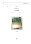
ENDCAP Alignment
ANALOG INTERFACE BOARD
User’s Manual
FNAL – PNPI
2003
Analog Interface Board
User’s manual
1. Introduction
The analog interface board provides a stable 11.3 V voltage for the R-sensors LPX50 and
Z-sensors ETI LCP8S-10, connection of the biaxial inclinometer ApGeo 900, R-, and Zsensors to a voltmeter, cross-connection of temperature (T) sensors, and low voltage
distribution for lasers. No control is required for this board.
2. Construction
The analog interface board has seven connectors:
J1
– 6-port RJ11 jack for connection:
Port 1 – the biaxial inclinometer
Port 2 – Z1 sensor
Port 3 – Z2 sensor
Port 4 – R1 sensor
Port 5 – R2 sensor
Port 6 – T1 sensor
J2
– 4-port RJ11 jack
Port 1 – Laser Output (This station)
Port 2 – Laser Input
Port 3 – T2 + T3 Input
Port 4 – T Output (T1 + T2 + T3)
J3
– RJ11 jack – Laser Output to the next station
J4, J5 – Low voltage distribution connectors
J6
– 3M 20-pin header – Output to a voltmeter
J7
– RJ11 jack – R3 sensor (used for ME1 only)
The analog interface board has four switches performed as pin strips controlled by shunts
(jumpers):
P1
– Select the input voltage for the Z1 sensor
One shunt is used always
P2
– Connect Z2 input voltage to the output connector J6
Two shunts are used simultaneously. If connection is not required, both
shunts should be placed to a single pin of the same switch.
Page 1 of 10
Analog Interface Board
User’s manual
P3
– Select the current board laser output
Two shunts are used always
P4
– Select a source for the channel 4 at the output connector J6 (pins 7, 8):
Z1 reference voltage or R3 sensor.
Two shunts are used always.
3. Circuit Diagram
The analog interface board consists of the low drop output (LDO) voltage regulator and
cross-connection circuitry. Voltage regulator is performed in LT1761 U1 integrated
circuit with external resistive divider R1, R2 that determines the output voltage as 11.2 V.
Red LED indicates a presence of the regulated voltage.
Page 2 of 10
Analog Interface Board
User’s manual
4. Application Notes
1. Admissible positions of shunt at the P1 switch are the following (any other
position is prohibited):
V1
P1
P1
V1
V2
V2
2. Admissible positions of shunts at the P1 switch are the following (any other
position is prohibited):
P2
J6:19
P2
J6:20
V2
J6:19
V2_GND
J6:20
V2
V2_GND
3. Admissible positions of shunt at the P1 switch are the following (any other
position is prohibited):
L3M
L3P
L2M
L2P
L1M
L1P
L3M
P2
L3P
L2M
L2P
L1M
L1P
L3M
L3P
P2
L2M
L2P
L1M
L1P
P2
4. Admissible positions of shunt at the P1 switch are the following (any other
position is prohibited):
Page 3 of 10
Z1VREF
R3
P4
Z1VREF
R3
P4
Analog Interface Board
User’s manual
5. Functioning
The analog interface board is a passive device representing a cross-connection board with
internal voltage regulator. It works properly if all settings and connections are correct.
6. Debugging and Testing
Necessary equipment:
o Digital voltmeter
o 12 – 15 V power supply
o Power cable for analog interface board
Properly manufactured analog interface boards do not require any adjustments and should
work correct at once.
1. Check the assembled board visually. It must not have visible damages. All
components and their values must be in accordance with documents.
2. Connect the analog interface board under test to the power supply 12 – 15 V and turn
on it. Check an input voltage after the F1 and F2 fuses; replace them if necessary.
3. Check +11.3V output voltage of the LDO voltage regulator.
4. A complete test of the analog alignment DAQ including the analog interface board
must be performed before a final assembly.
7. Troubleshooting and Maintenance
Output voltage of the voltage regulator is wrong.
•
•
•
•
•
Check an input voltage; it should be 12 – 15 V.
Check a fuse F2; replace it if necessary.
Check values of the R1 and R2 resistors.
Check polarity of the C6, C8, and C9 tantalum capacitors (a white band marks
a positive pad).
If the previous checks do not discover a reason of failure, replace the U1
LTC11761 integrated circuit.
Page 4 of 10
Analog Interface Board
8.
User’s manual
Specification
General
Dimensions of the board
Input connector J1
Input/output connector J2
Output connector J3
Power connectors J4, J5
Output connector J6
Switch P1
Switch P2
Switch P3
6.7” x 2.9”
6-port RJ11 jack
4-port RJ11 jack
RJ11 jack
2-pin Molex Sabre 43160-3102
20-pin 3M header 3428-6002
3-pin single raw strip 3M 929647-09-36-I
(modified) with shunt 3M 929957-08
2 x 2 double raw strip 3M 929665-09-36-I
(modified) with shunts 3M 929957-08
6 x 2 double raw strip 3M 929665-09-36-I
(modified) with shunts 3M 929957-08
Power characteristics
Minimum input voltage
+12 V
Maximum input voltage
+15 V
Output regulated voltage
+11.2 V
Power consumption:
480 mW with entire sensor set
Current consumption:
Inclinometer
7 mA
R-sensors
2 x 1.13 = 2.26 mA
Z-sensors
2 x 11.3 = 22.6 mA
On board power protection:
Two fuses
0.5 A
LT1761 voltage regulator has overcurrent and overtemperature protection
Specification of connectors
Connector J1 port 1 (Inclinometer Input):
Pin
1
2
3
4
5
6
Name
VX
GND (VX)
VY
GND (VY)
VIN
GND
Page 5 of 10
Analog Interface Board
User’s manual
Connector J1 ports 2 – 5 (Z1, Z2, R1, R2):
Pin
1
2
3
4
5
6
Name
VWIPER
GND (W VWIPER)
VREF
GND (VREF)
VIN
GND
Connector J1 port 6 (T1 Input):
Pin
1
2
3
4
5
6
Name
T1T1+
Connector J2 port 1 (Laser Out):
Pin
1
2
3
4
5
6
Name
Laser Output +
Laser Output -
Connector J2 port 2 (Laser Input):
Pin
1
2
3
4
5
6
Name
Laser 1 Input +
Laser 1 Input Laser 2 Input +
Laser 2 Input Laser 3 Input +
Laser 3 Input -
Page 6 of 10
Analog Interface Board
User’s manual
Connector J2 port 3 (T2 + T3 Input):
Pin
1
2
3
4
5
6
Name
T2T2+
T3T3+
Connector J2 port 4 (T Output):
Pin
1
2
3
4
5
6
Name
T1T1+
T2T2+
T3T3+
Connector J3 (Laser Output to the next station):
Pin
1
2
3
4
5
6
Name
Laser 1 Output +
Laser 1 Output Laser 2 Output +
Laser 2 Output Laser 3 Output +
Laser 3 Output -
Connectors J4, J5 (Low voltage distribution):
Pin
1
2
Name
PWR
GND
Page 7 of 10
Analog Interface Board
User’s manual
Output connector J6:
Name
Pin
1
3
5
7
9
11
13
15
17
19
VX
VY
VZ1W
VZ1R or VR3*
VZ2W
VR1W
VR1R
VR2W
VR2R
<VZ2R>**
*
**
Pin
2
4
6
8
10
12
14
16
18
20
Name
GND (VX)
GND (VY)
GND (VZ1W)
GND (VZ1R or VR3) *
GND (VZ2W)
GND (VR1W)
GND (VR1R)
GND (VR2W)
GND (VR2R)
<[GND (VZ2R)> **
Selected by P4
If P2 shunts are inserted
Connector J7 (R3):
Pin
1
2
3
4
5
6
Name
VWIPER
GND (VWIPER)
VIN
GND
Page 8 of 10
Analog Interface Board
User’s manual
Fig. 1. The analog interface board
Page 9 of 10