1
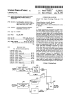
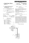
Illllllllllllllllllllllllllllllllllllllllllllllllllllllllllllllllllllllllll
US005119082A
United States Patent [19]
[11]
[45]
Lumelsky et a].
[54]
5,119,082
Date of Patent:
Jun. 2, 1992
COLOR TELEVISION WINDOW
EXPANSION AND OVERSCAN
OTHER PUBLICATIONS
CORRECTION FOR HIGH-RESOLUTION
“Digital Image Processing", by Gregory A. Baxes, pp.
RASTER GRAPHICS DISPLAYS
l60—16l, 1984.
Inventors: Leon Lumelsky, Stamford, Conn.;
Philips Co. SIGNETICS; Digital Video Signal Proces
wig-Pan one‘
Sung Min Choi, White Plains; Alan
w- Peevers, Peekskill, bOth of NY.
[731
Patent Number:
Assignee:
Primary Examiner—Alvin E. Oberley
Assistant Examiner-Amare Mengistu
Attorney, Agent, or Firm-Roy R. Schlemmer; Jack M.
Arnold
International Business Machines
Corporation, Armonk, NY.
[57]
ABSTRACT
A video pixel presentation rate expansion circuit is pro
vided for use with a high-resolution display system. The
overall display system includes a high-resolution moni
tor, a computer for providing control signals, including
[21]
Appl. No.: 415,012
[22]
Fned:
[51]
Int. Cl.-‘ ....................... .. G096 1/06; H04N 9/74;
video data at a rate controlled by said control signals
HMN 7/01
and providing said data with a high-resolution monitor
[52]
US. Cl. .................................. ..
for
[58]
_
340/814; 353/22; 358/140
Field of Search ..................... .. 340/717, 814, 731;
358/22: 140
tion comprises means responsive to an expansion pat
‘cm generated by the computgr for changing the time
base of the video pixel data read out of said frame
buffer. Circuit includes means responsive to said expan
sell 29 1989
’
a high-resolution frame buffer for storing computer
graphics and TV video images and reading out said
References Cited
[56]
The expansion circuit of the present inven
sion pattern for selectively repeating predetermined
‘
scan lines of said video display and for selectively re
U‘S' PATENT DOCUMENTS
peating certain pixel along a given scan line to match
4,063.280 12/1977 Hattorie et al. ............. .. 358/22 P1P
4.121.283 10/ 1978 Walker ----------- -340/703
HUI'SI ................................. ..
the time base of the video data read out of said frame
buffer to the time base of said high-resolution monitor.
According to a preferred embodimen‘ of the invention
4'303'986 12/1931 L?“ '
the expansion circuit functions to modify the control
45]” ‘4 2/1982 walker '
4.686.580
8/1937
4 746 979 5/1988
4,746,981 5/1988
signals which controls the read-out of the frame buffer
.
.
.
.
. .
.
in a predetermined fashion without any additional video
bum" Slorage means
358/451
358/22
340/717
4,82l.03l
4/1989
4,952,923
8/1990 Tamura ............................. .. 340/731
.. 340/73]
Y
5 Claims, 5 Drawing Sheets
Y
A
B
C
D
E
F'
G
H
I
(B-Y)
A
B
C
D
E
F
G
H
I
(R-Y)
A
B
C
D
E
F
G
H
I
A
A
B
C
C
D
E
E
F
F
G
H
I
(B-Y)ABCDABCDEFGHI
(R-Y)ABCDABCDEFGHI
US. Patent
June 2,1992
Sheet 1 of s
TV IMAGE
‘
5,119,082
HIGH RESOLUTION IMAGE
Is
FIG.I
Id
Q ____
Q
f ___________________________ "I\
T
l
I
I
FIGZA
f
I
v
\
T
I
I
I
l
Tv
AIIHIES
I
I
'
VISIBLE
I
PORTION
I
I
I
OF THE
SCREEN
;
:
I L
'
'
390
480
J i
I
I
il
_____________________________ .,
)
6I2 PELS
ACTIVE VIDEO 720
f
a
r/ /////////////////////7\
;Z
FIG. 2B
j;
/
ACT'VE
4
480 LINES
?
HI-RES VIDEO
4
0R HIGHER
2
§
/
/
/
4
’/f///////////////////// /
\
1
__AcIIvE VIDEOI64O PELS) OR
HIGHER _'
U.S. Patent
June 2, 1992
Sheet 3 of 5
FIGAA
PRIOR ART
(B-Y)
A
(R-Y)
A
FIGAB
(B-Y)
A
(R-Y)
A
5,119,082
US. Patent
June 2,1992
=
Sheet 5 of5
1
1
'
5,119,082
l
1
j
1
HXSR(0)
VSCLK
"-1
1-
VIDEO DATA
FROM
1
FRAME BUFFER ‘- A
VCLK'
D/A
—L
B
'"_—L
I
‘__1
,
‘_A ‘AFB
VIDED
DATA IN
~
‘
(
704
12
702
’
E
.
‘
D
VIDED
DATA BUT
VIDEU
SOURCE‘?>
'
D
‘-—-—-‘
DATA
LATCHED
FIG 7
<
C
TU
VIDEO
A DISPLAY
BUFFER
VCLK’
-—-—----vscu<
VBADDR
VIDED BUFFER
ADDRESS MULTIPLEXER
706
1
5,119,082
2
store away incoming pixels such that they are not lost,
COLOR TELEVISION WINDOW EXPANSION
AND OVERSCAN CORRECTION FOR
HIGH-RESOLUTION RASTER GRAPHICS
DISPLAYS
or a mixture of both.
It should be noted that as the magni?cation ratio
increases, the image quality decreases. For example,
when the magni?cation ratio is greater than two, the
sharpness of the image is greatly reduced.
Nevertheless, for current mixed video/graphics dis
FIELD OF THE INVENTION
The present invention relates generally to the ?eld of
raster-scan graphic/video display systems. More partic
ularly, it relates to such display systems which are capa
play systems, the signi?cance of magnifying television
images are of considerable importance. It is especially
0 important due to overscan problems which will be dis
cussed below.
In conventional commercial TV systems, the active
portion of the raster (i.e., between blank signals) over
ble of displaying interchangeably and/or concurrently
both high-resolution graphic data and standard lower
resolution TV video data on a high-resolution graphics
monitor.
scans the viewing area of the CRT to prevent a black
border under worst-case conditions of variations in
yoke sensitivity, anode voltage, etc. (See “Television
Engineering Handbook", McGraw Hill Company,
CROSS REFERENCE TO RELATED
APPLICATIONS
Window For a Video Display Unit“ discloses a video
1986, p.l3.l77). The overscan requirement for con
sumer TV receivers goes somewhat higher than 10% of
the full active area (See FIG. 2). This means that less
than 90% of the active video image is usually shown on
adapter architecture which provides for the expansion
a TV screen. It is safe to say that video is overscanned
US. patent application Ser. No. 314,998, ?led Feb.
24, 1989 of Lumelslty et al., Entitled “Color-Television
of video data before it is stored in the video frame
not more than 15%. This number is taken into consider
ation when video is edited.
buffer. It performs the requisite time-base or pixel pre
On the other hand, high-resolution graphics monitors
sentation rate expansion on the data at the input to the 25
video frame buffer and requires signi?cant extra hard
ware to perform this operation contrasted with the
present invention.
BACKGROUND OF THE INVENTION
do not use an overscan approach. Rather, they are un
derscanned in order to present all graphics image pixels
on the screen. In other words, it means that a black
30
The mapping of a television image on a graphics
screen generally requires the image to be sampled and
stored into a frame buffer. This allows a time base cor
rection to be provided and, if necessary, a time com
pression of the television image in order to show both
television and graphics images on the same screen. If
the image should be positioned in any arbitrary sized
border always surrounds the image.
The majority of applications in the multimedia area
overlay a television image with graphics. The most
widely used approach is to match 85% (in both linear
directions) of the active television video with full
lengths of the active graphics video line. With this ap
proach a multimedia editor can be sure that whatever
television movies or other materials are combined with
graphics, the television image coordinates will corre
spond to the graphics image coordinates with reason
window on a graphics screen, it should be either scaled
up or down. The image itself may not be a full screen
able accuracy. and no unnecessary information, which
image, but just an arbitrary window inside the full view
image. This requires a translation and scaling operation
screen.
on the source image. Translation is a simple matter, and
shall not be discussed in this paper. FIG. 1 shows how
viding compatibility with previously developed multi
might be overlooked during editing, will appear on the
The overscan requirement is also important for pro
media programs. For example, millions of dollars are
a TV image window, Is, is transposed to a graphics 45 spent on such video processing programs such as IBM
screen window, Id.
Scaling up a television image on a graphics screen
poses a much harder problem than scaling down. When
scaling down a source image to a smaller destination
image, it is possible to simply ignore pixels in the hori
zontal direction and ignore scan lines in the vertical
direction to achieve the correct sizing at the time of
sampling. For example, to achieve a quarter sized win
dow, every other pixel can be thrown away horizon
tally, and every other scan line vertically. This can be 55
done simply at the time of sampling the source image
into a frame buffer. However, for image expansion, it is
necessary to either replicate pixels in a horizontal direc
tion or replicate scan lines in a vertical direction to
achieve the desired destination window size. This poses
a problem as the bandwidth of the frame buffer needs to
be increased. For example, if it were necessary to don
ble the source image in both horizontal and vertical
Infowindow, educational and presentation programs,
where the overscan is taken into consideration. For a
detailed description of the Infowindow product, refer
ence should be made to one of the following publica
tions describing same.
1) “Infowindow Guide to Operations" Order No.
SK2T0297 and,
2) “Infowindow Enhanced Graphics Adapter: I-Iard
ware Maintenance and Service Manual" Order No.
SK2T0298, both are available from IBM Corp.
Mechanicsburg, Pa. Any multimedia display
adapter which does not address the overscan prob_
lem can not be used with Infowindow or Infowin
dow-like programs. Moreover, such an adapter can
not be used with the television material edited ?rst
on standard television editing equipment.
In the case of the IBM Infowindow product, a special
enhanced graphics adapter (EGA) monitor is used
directions, the bandwidth of the frame buffer required
which provides for the overscan of video. It is, how~
to achieve the expansion needs to be quadrupled. The 65 ever, not a common graphics monitor. The approach of
result of this is that either a faster frame buffer memory
the present invention allows the use of a standard
is necessary (notice that the speed of the frame buffer
depends on the enlarging ratio), a FIFO deep enough to
scan by a special sampling approach. Such a monitor
graphics monitor, providing the television image over
3
5,119,082
4
bits of B-Y and 8 bits of R-Y). This further complicates
expansion in the horizontal direction since due to the
time multiplexing, it is not possible to simply replicate
pixels. Notice that for chrominance, the smallest hori
Zontal resolution is 4 pixels wide. It is necessary to keep
architecture is disclosed and described in the publica
tion “IBM lnfowindow Color Display" No. ZR23-6820
available from the IBM Corp. Mechanicsburg, Pa.
One possible solution to achieving overscan is to
choose a television image sampling frequency higher
than that of the graphics video clock frequency. E.g., if
the synchronization of the chrominance bits over a
IBM PS/2 VGA has a video clock frequency of 25 Mhz
which corresponds to 640 pixels on the active portion of
period of four system clock cycles, and failing to do so
horizontal scan line, the video sampling frequency
should provide 640 pixels on the active portion of the
all pixels that are out of synchronization.
will result in corrupt color on the destination screen for
Prior Art
underscanned television horizontal scan line. Therefore,
a total of 752 samples are required per scan line to
achieve 640 pixels of underscanned samples (e.g.,
7524859). Hence, 640 pixels of the sampled video image
will correspond to 640 graphics pixels exactly, and the
overscan requirement is satis?ed.
This approach, however, does not work well when
using the standard digital television sampling fre
quency. Frequently, the television image is decoded and
sampled using standard digital television techniques. It
provides a cheaper solution, better image quality, and
easier control over the brightness, sharpness, hue, etc.
Unfortunately, the CCIR 60l-l recommendation for
digital television encoding and transmission (See
No video adapter architectures or hardware systems
are known to the inventors which solve the above de
5
scribed problems using methods or apparatus at all simi
lar to the herein disclosed expansion hardware mecha
nism.
SUMMARY AND OBJECTS
It is a primary object of the present invention to pro
vide a cost effective method and apparatus for expand
ing video image data stored in a frame buffer in digital
format in both the X and Y directions.
It is a further object of the invention to provide such
method and apparatus that operates strictly on the
“Handbook of Recommended Standards and Proce 25 frame buffer output and provides certain control signals
dures, International Teleproduction Society”, 1987, p.
62), which is widely used in the television industry,
prescribes a sampling frequency of l3.5 Mhz. It gives a
total of only 720 samples on a television scan line. With
15% overscan, it allows only 612 pixels as shown on
FIG. 2. The present invention comprises a system for
mapping 612 samples of the television image (pixels)
to the output of the frame buffer for replicating prede
termined scan lines and pixels but does not require any
additional video buffering hardware.
It is another object of the invention to provide such a
method and apparatus wherein the only change in the
video data path between the frame buffer and the moni
tor is the provision of modi?ed clocks for accessing
onto a larger number of graphics pixels.
Clearly, the solution which preserves the sampling
rate is to increase the number of samples after sampling
has been done. Using the standard sampling rate of 13.5
Mhz, if the number of graphics pixels is 640, then the
expansion ratio should be 640/604. However, this num
both individual scan lines and pixels from the frame
buffer wherein certain scan lines and pixels may be
ber is not a power oftwo, and the expansion can not be
drawings and claims.
selectively repeated.
Other objects features and advantages of the inven
tion will be apparent from the following description of
the invention as set forth in the appended speci?cation,
done in a simple way, like replicating every pixel. An 40 The objects of the present invention are accom
other consideration is that if the graphics adapter has
plished in general by a video expansion circuit for use
several modes with a different number of pixels in the
with a high-resolution display system. The overall dis
horizontal line, e.g., 320, 640, 720 pixels in the case of a
play system includes a high-resolution monitor, a com
VGA graphics adapter, (See, for example, IBM PS/2
puter for providing control signals,.a high-resolution
Model 80 Technical Reference #68X2256 available
frame buffer for storing computer graphics data and a
from the IBM Corp. Mechanicsburg, Pa.) the scaling
video frame buffer for storing TV video data and a
ratio should be programmable. In a window environ
ment, the expansion ratio should ideally be selectable to
be any rational number de?ned by the size of the win
dow.
This situation is even more complicated by the spe
mechanism for reading out the video data at a rate con
ci?c coding scheme of digital television. The standard
television coding schemes, either NTSC, PAL, or
SECAM are all based on luminance/chrominance
(Y /C) representations, rather than RGB, which reduces
the bandwidth of the composite video signal and mem
ory required to store the image frame. Furthermore, ‘
some digital television chips already in production use a
time multiplexing technique to reduce the bandwidth
required for chrominance information. For example,
Philips provides digital television chips (See, for exam
ple, "Digital Video Signal Processing" Philips Compo
nears Manual N0. 9398 063 30011) in which luminance
bit rate versus color bit rate is 4:]. Compared to 8 bits of
trolled by said control signals and providing the video
data to the high-resolution monitor for display.
The expansion circuit of the present invention com
prises a mechanism responsive to an expansion pattern
generated by the computer for changing the rate of
video pixel data read out of the frame buffer. The circuit
includes such a mechanism responsive to the expansion
pattern for selectively repeating predetermined scan
lines of the video display and for selectively repeating
certain pixels along a given scan line to allow the video
data read out of the frame buffer to be expanded on the
high-resolution monitor.
'
According to a preferred embodiment of the inven
tion the expansion circuit functions to modify the con
trol signals which control the read-out of the frame
buffer in a predetermined manner without any addi
tional video buffer storage. In the simplest form of the
luminance information per sampling clock, only 4 bits 65 invention the additional circuitry required comprises
of chrominance are generated (2 bits for B-Y and 8 bits
of R-Y) as shown in FIG. 3. Thus it takes four clock
cycles to transmit a complete chrominance values (8
only two registers for holding the generated expansion
patterns in the horizontal and vertical direction and two
shift registers for receiving these patterns and process
5
5,119,082
6
ing same to alter the frame buffer clocks to achieve
possible to achieve this effect by controlling the system
replication of predetermined lines and pixels as deter
mined from the said expansion patterns.
clock to the D/A chip as explained below.
Although implementation of the present invention
may be accomplished in many different ways, e.g., by a
BRIEF DESCRIPTION OF THE DRAWINGS
counter, a shift register, or a random access memory, all
operating under control of the desired expansion pat
FIG. 1 is a diagramatic representation of the mapping
tern a shift register is utilized herein because of its sim
plicity and cost factors.
For the vertical direction, the hardware required is
of the window portion of a television window onto a
larger high-resolution graphics display screen window.
FIG. 2 A is a graphical representation illustrating
relationship of the total active video data sent to a stan
quite simple. (See the block diagram of FIG. 5.) Refer
dard TV receiver with respect to the actual video data
ring brie?y to FIG. 7 video data ?ow in a typical video
adapter for a high-resolution display is shown. The
analog VIDEO SOURCE 700 is digitally converted
into 12 bit data pixels of Y/C representation with the
presented on e.g., visible on the TV screen.
FIG. 2 B comprises a graphical representation illus
trating the presentation of high-resolution video/graph
ics data on a high-resolution screen.
15
FIGS. 3 A and 3 B are a diagrammatic representation
of one prior-art digital-television technique for repre
senting a_ color television signal, wherein FIG. 3 A
illustrates the representation of the actual luminance
chrominance time multiplexing technique illustrated in
FIG. 4 B. This video data passes over (VIDEO DATA
IN) line 702 and is stored in the VIDEO BUFFER 704.
Digitized video pixels (VIDEO DATA OUT) are
serially scanned out of the VIDEO BUFFER 704 with
and chrominance data and wherein FIG. 3 B illustrates 20 the VIDEO Scan Clock (VSCLK). When VSCLK is
inhibited, the same pixel is repeated for as long as it is
the way in which the chrominance data is encoded and
inhibited.
'
combined with the luminance data for transmission
VIDEO DATA OUT is converted to analog signal
and/or storage to conserve bandwidth.
via D/A using VCLK'.
FIG. 4 A comprises a diagram similar to FIG. 3 B
illustrating consecutive pixels of luminance and chromi
The Video Buffer Address (V BADDR) which con
nance data of a digital TV video signal as it would be
conventionally stored in a video frame buffer utilizing
trols access to successive lines of data in the VIDEO
BUFFER is done with a multiplexer 706 and one of the
the time multiplex technique.
inputs to this multiplexer is VREF. It will be noted that
VREF', VCLK', and VSCLK are generated by the
ing digital TV data illustrating a 2:3 expansion the video 30 circuitry shown on FIG. 5.
Before proceeding with a description of FIG. 5; the
data illustrated in FIG. 4 A showing how certain lumi
following terms should be de?ned:
nance groups are repeated while at the same time con
The Vertical Synchronization pulse (—VS): tell that
serving the original format for the chrominance data.
a new frame is about to be displayed.
FIG. 5 comprises a functional block diagram of
FIG. 4 B is a diagrammatic illustration of the result
herein disclosed preferred embodiment of the expansion
circuit of the present invention.
The Horizontal Synchronization pulse (—-I-IS): tell
that a new scan line is about to be displayed.
FIG. 6 comprises a timing diagram illustrating the
operation of the expansion circuit of FIG. 5.
The Video Clock (VCLK): comprise system’s pixel
FIG. 7 comprises a high level functional block dia
gram illustrating the video data ?ow within such a
video buffer system in which the present invention has
The Video Scan Clock (V SCLK): derived from
particular application.
DESCRIPTION OF THE DISCLOSED
EMBODIMENT
45
The basic concept of the present invention comprises
scaling up the image at the frame buffer output instead
of at the frame buffer input. Expansion in the vertical
direction is a simple matter since it is possible to display
the same scan line multiple times. This can be imple 50
clock.
VCLK. On every transition of VSCLK from 0 to
1, 12 bits of pixel data (VIDEO DATA OUT) is
' shifted out of the VIDEO BUFFER to the display
via the digital analog cltt. D/A.
The Video Clock to D/A (VCLK'): derived from
VCLK. On every transition of VCLK’ from 0 to 1,
12 bit pixel data (VIDEO DATA OUT) is taken by
the D/A converter.
The host computer initializes 3 registers.
1) Vertical Expand Pattern Register (VXPR)
——Holds vertical expansion pattern
mented very cheaply by disabling the vertical display
2) Horizontal Expand Pattern Register (I-IXPR)
scan line counter from incrementing whenever it is
—Holds horizontal expansion pattern
3) Vertical Scan Line Register (V SLR) —-Holds ?rst
necessary to repeat a scan line.
Expansion in a horizontal direction is not as simple,
however. Due to the chrominance, time-multiplexing 55
technique utilized in such digital TV systems, it is not
possible to simply replicate the pixels since that will
corrupt the phase of the chrominance packets, produc
scan line address of the VIDEO BUFFER to be
displayed.
The function of the Vertical Expand Shift Register 12
(V XSR) is to vertically expand the displayed pattern by
allowing a given horizontal line to be repeated. When
ing erroneous colors. The necessary chrominance pack
-VS is 0, VXSR 12 is loaded with the contents of the
ets are shown in FIG. 4 A. As will be noted the chromi
Vertical Expand Pattern Register (VXPR) 10. On every
nance packet which accompanies a particular replicated
pixel does not necessarily correspond to the original
transition of —HS from 0 to 1, VXSR is rotated (end
around shift) I bit. Whenever the least signi?cant bit
(VXSR<0>) is set, it signifies that the same scan line
chrominance packet as illustrated in FIG. 4 B.
currently being displayed should be repeated. The oper
To guarantee that the color does not get corrupted, it
is necessary to disable the D/A chip for a clock cycle of 65 ation of Vertical Scan Line Counter 14 (V SLC) is as
follows. It is used as a pointer to specify which scan line
the time of the replication to keep the D/A chip in step
of the VIDEO BUFFER is going to be displayed.
with the frame buffer. Normally a video D/A chip set
When —V5 is 0, this speci?es that a new frame is about
does not have this capability built into it. However, it is
5,119,082
7
to be displayed, thus the ?rst scan line address stored in
the (VSLR) 16 of the VIDEO BUFFER is loaded into
the VSLC. On every transition of —I-lS from 0 to 1, if
VXSR <0> is set, then VSLC remains the same, (thus
pointing to the same scan line) else VSLC is incre
mented. (Thus pointing to the next scan line) The opera
8
CONCLUSION
The disclosure provides a solution to the real time
color motion video image expansion with arbitrary
zooming ratio, providing a single video window or
equal expansion of several video windows, which are
sampled within the same image frame buffer. The inven
tion of the Horizontal Expand Shift Register (I-IXSR)
tion
is especially important when a television image is
20 is as follows. It is used to expand the video data line
sampled according to the standard digital television
horizontally.
10 techniques. Furthermore, the invention solves the com
When —I~IS is 0, HXSR 20 is loaded from the Hori
patibility problem of overlaying previously taken video
zontal Expand Pattern Register 18 (I-IXPR). On every
material with a variety of graphics controllers, each
transition of VCLK from 0 to l, I-IXSR is rotated (end
having different resolution and pixel video clocks.
around shift) 1 bit. Whenever the least signi?cant bit
By adding two registers, 2 shift registers, 1 ?ip-?op,
(I-IXSR <0>) is set, it signi?es that the same pixel being
and 2 OR gates it is possible to achieve the bi-direc
displayed should be repeated.
tional image expansion of the present invention. As will
The operation of the D-Q Flip Flop 22 is to delay the
be readily appreciated, the cost of doing this is either
least signi?cant bit of HXSR 20 (HXSR<O>) for l
less than in a ?rst category of prior art systems or is
VCLK cycle. This in effect delays VCLK’ l clock
much more accurate than other prior art systems which,
cycle from VSCLK (See FIG. 6).
20
The function of OR gates 24 and 26 is to deactivate
VCLK' and VSCLK (See FIG. 6) e.g., if the ?ip-?op 22
‘for example, change the video output clock frequency
using analog means.
I
Thus, by utilizing the present invention, which oper
ates on the output of the frame buffer, controls are
is set VCLK' and VSCLK are inhibited.
provided which automatically cause speci?ed pixels
Referring now to FIG. 6, the overall timing of the
system may be seen. VCLK is the free running system 25 and lines in the video output to be repeated by control
ling the serial port of the buffer “on the fly” without
clock for the display. When I-IXSR<0> is I, this sup
signi?cantly
increasing the buffer hardware and cost.
presses VSCLK from going to 0 (Using OR gate 24).
It should be noted that, as mentioned before, shift
Since the scan clock to the VIDEO BUFFER is sup
registers were chosen for use in the control circuitry for
pressed, the same VIDEO DATA OUT is available for
providing the expansion patterns for both horizontal
2 VCLK cycles (See the VIDEO DATA from the
and vertical directions. However, there is no reason
Frame Buffer curve on FIG. 6 whereby pixel “C" is
why other obvious methods or instrumentalities cannot
repeated).
Using the ?ip-?op 22 and OR gate 26, VCLK' is
delayed 1 VCLK cycle from VSCLK. Notice that this
is necessary to ensure that the D/A device does not
sample the VIDEO DATA OUT twice (pixel “C")
(See FIG. 6). Unless VCLK' of the 4th clock cycle is
suppressed, the “C" data would be latched twice by
be used to provide these patterns. For example, two
RAM's can be used to provide the patterns. One RAM
would provide the pattern for the horizontal expansion
and the other RAM would provide the pattern for the
vertical expansion. These RAM‘s would be preloaded
by the host computer with the expansion pattern.
It should be again noted that the means of providing
D/A device. This would cause an incorrect chromi'
nance pattern.
the patterns is independent of the disclosure. Any
method that provides two expansion patterns would
It should be noted that the particular expansion pat
tern (rates) required can be easily provided by software
in the host computer.
work with the present invention as long as it adhered to
FIG. 4 shows 2:3 image expansion with a time multi 45
plexing technique. Notice that luminance bits are simply
replicated at every other pixel, but chrominance bits
must be replicated by groups of four pixels to avoid
losing chrominance data. An 8 bit expansion pattern for
this would be 01010101.
'
The computation of the expansion patterns in both
the horizontal and vertical directions would be obvious
to those skilled in the art. The above example assumes a
2:3 expansion. By way of further example if a 8:10 (4:5)
expansion were desired an 8 bit expansion pattern
00010001 would provide this. Thus every bit (line) hav~
ing a “0" in the expansion ?eld would be sent to the
display once, whereas every bit (line) having a "l" in
the expansion ?eld will be repeated. An expansion pat
tern 00010000 would produce a 8:9 expansion.
For a description of a more generalized algorithm for
the following rules:
1) A horizontal pattern bit is provided per pixel, and i
the same horizontal expansion pattern sequence is
repeated on every scan line.
2) A vertical pattern bit is provided per scan line, and
the same vertical expansion pattern sequence is
repeated on every frame.
As clearly indicated above, many changes may be
made in the circuits and processes speci?cally described
herein without departing from the spirit and scope of
the instant invention, and it is intended to encompass all
other embodiments, alternatives, and modi?cations con
sistent with the invention.
We claim:
1. In a high-resolution display system including a
high-resolution monitor, a computer including a frame
buffer and means for generating timing and control
signals for reading out video data stored in said frame
buffer, in a digital luminance/chrominance (Y/C) X:l
format wherein the chrominance data fully representing
the proper chrominance value for a plurality (X) of
computing the expansion pattern, reference may be
made to referenced copending application Ser. No.
luminance pixels is time-multiplexed with related lumi
314,998 in the section entitled A. Image Expansion. It 65 nance pixels so each "m" bit chrominance data signal is
should be clearly understood that the method by which
split between m/x consecutive Y/C video signal pack
the expansion pattern is generated is not within the
ets, so that each luminance pixel ?eld is associated with
an m/x bit chrominance data ?eld, a digital-to-analog
purview of the present invention.
9
5,119,082
10
converter (DAC) for connecting the digital video data
data, and sent to the monitor when a particular pixel is
to an analog format, for display on the monitor said
repeated.
signals including a pixel clock, a horizontal sync signal
and a vertical sync signal and expansion pattern gener
ating means which includes a speci?cation of the scan
lines which are to be repeated in a given frame and the
3. A pixel presentation expansion mechanism as set
forth in claim 2, wherein both said first and second
means include vertical and horizontal expansion regis
ter means for receiving and storing vertical (scan line)
pixels which are to be repeated in each scan line, the
and horizontal (pixel) expansion patterns respectively
improvement which comprises a pixel presentation ex
generated by said computer and shift register means for
pansion mechanism located between the frame buffer
output and the monitor input for altering the frame
buffer access controls, including
receiving said respective expansion patterns and circuit
means for successively examining each scan line and
pixel expansion pattern to determine if a particular scan
line or pixel is to be repeated and means for inhibiting
?rst means for causing selected adjacent scan lines to
scan line address generating circuit and pixel chromi
be repeated as they are read out of the frame buffer,
nance data, accessing circuitry respectively, if said scan
and
second means for causing the luminance data signal of 15 line or pixel is to be repeated.
4. A pixel presentation expansion mechanism as set
the selected pixels in all the can lines of a particular
forth in claim 3, including means for periodically load
frame to be repeated as they are read out of the
ing the vertical expansion register and loading the con
frame buffer, and for maintaining the correct ac
tents thereof into the vertical shift register once per
cessing of sequential time-multiplexed m/x bit
chrominance data ?elds by the DAC to prevent the 20 frame in synchronism with the scan line frequency of
the-monitor and wherein the size of the expansion regis
erroneous combination of chrominance data ?elds
ter and shift register is the same.
(C) accompanying repeated luminance data ?elds
5. A pixel presentation expansion mechanism as set
forth in claim 3, including means for periodically load
in the analog signal presented to the monitor.
2. A pixel representation expansion mechanism as set
forth in claim 1. wherein said second means further 25 ing the horizontal expansion register and loading the
contents thereof into the horizontal shift register once
includes means for inhibiting the transferring of chromi
per scan line in synchronism with the pixel presentation
nance bits to said digital to analog converter located
frequency of the monitor and wherein the size of the
between the output of the frame buffer and the input to
expansion register and shift register is the same.
the display monitor to prevent erroneous chrominance
I
data from being decoded, combined with luminance
35
45
50
55
65
i
i
3
$