1
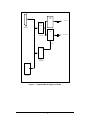
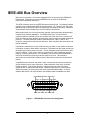
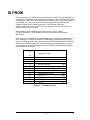
IP-488
IEEE-488 (GPIB)
Instrumentation Bus
IndustryPack®
User Manual
©SBS Technologies, Inc.
Subject to change without notice.
Hardware Revision: D
Part # 89002057 Rev. 1.1
20050505
IP-488
IEEE-488 (GPIB)
Instrumentation Bus
IndustryPack®
SBS Technologies, Inc.
1284 Corporate Center Drive
St. Paul, MN 55121
Tel (651) 905-4700
FAX (651) 905-4701
Email: [email protected]
http://www.sbs.com
©1999, 2005 SBS Technologies, Inc.
IndustryPack is a registered trademark of SBS
Technologies, Inc. QuickPack, SDpacK and Unilin
are trademarks SBS Technologies, Inc. PC•MIP is a
trademark of SBS Technologies, Inc. and MEN
Mikro GmbH.
SBS Technologies, Inc acknowledges the
trademarks of other organizations for their
respective products mentioned in this document.
All rights are reserved: No one is permitted to
reproduce or duplicate, in any form, the whole or
part of this document without the express consent of
SBS Technologies, Inc. This document is meant
solely for the purpose in which it was delivered.
SBS Technologies, Inc. reserves the right to make
any changes in the devices or device specifications
contained herein at any time and without notice.
Customers are advised to verify all information
contained in this document.
The electronic equipment described herein
generates, uses and may radiate radio frequency
energy, which can cause radio interference. SBS
Technologies, Inc. assumes no liability for any
damages caused by such interference.
SBS Technologies, Inc.’s products are not
authorized for use as critical components in medical
applications such as life support equipment, without
the express consent of the general manager of SBS
Technologies, Inc. Commercial Group.
Table of Contents
Product Description ........................................................................................................................5
VMEbus Addressing.......................................................................................................................7
NuBus Addressing..........................................................................................................................8
Programming...................................................................................................................................9
User Options .................................................................................................................................10
IEEE-488 Bus Overview ..............................................................................................................11
ID PROM........................................................................................................................................12
I/O Pin Wiring ................................................................................................................................13
Construction and Reliability ........................................................................................................14
Repair .............................................................................................................................................15
Specifications ................................................................................................................................16
List of Figures
Figure 1
Figure 2
Figure 3
Figure 4
Figure 5
Figure 6
Simplified Block Diagram of IP-488 .........................................................................6
VMEbus Register Map ................................................................................................7
NuBus Register Map ...................................................................................................8
IEEE-488 Bus Connector Pin Assignment ...........................................................11
ID PROM Data (hex) ................................................................................................12
IP-488 I/O Pin Assignment......................................................................................13
Product Description
IP-488 is part of the Industry Pack™ family of modular I/O components. It provides
talker, listener and controller access to the IEEE-488 instrumentation bus (GPIB). IP-488
is compatible with IEEE-488.1 and IEE-488.2.
IP-488 is a straight forward implementation of National Instruments' NAT9914A. The
NAT9914A is pin for pin compatible with Texas Instruments' popular TMS9914A with
enhanced capabilities (i.e IEEE488.2). Users will find both programming and
applications easier if they have reference to the Texas Instruments' "TMS9914A General
Purpose Interface Bus (GPIB) Controller Data Manual," the "TMS9914A GPIB Controller
User's Guide" (document no. SPPU013), and National Instruments' NAT9914A
IEEE488.2 data sheet. These documents are available from Texas Instruments and
National Instruments.
The interface from the 9914A to the IP carrier is conventional, using 8-bits only on odd
bytes. The base address of the chip is the same as the base address assigned to the IP
slot on the IP carrier board. Two additional addresses are implemented outside the chip
to read the 6-bit address switch and access the interrupt vector register. These
addresses are shown in the address maps shown in the next sections. The LSB of the
vector register also serves as a control line for the System Controller function (SC).
The interface from the 9914A to the instrumentation bus is implemented with two Texas
Instruments octal transceivers designed specifically for this purpose: 75ALS160 and
75ALS164. These parts feature: direct control by the 9914A (except for SC), bus
terminating resistors, glitch free power-up and power-down, and receiver hysteresis. The
bus interface lines are protected from ESD damage by SBS’ unique LineSafe™
protection circuit. The same filters attenuate any EMI to help the final system meet
FCC/CE EMI standards.
All control circuitry, the ID PROM, and the interrupt vector register is implemented within
an Altera EPM7032.
A simple interrupt architecture uses a single programmable vector for all 9914A
interrupts. Two 8-bit interrupt status/mask registers inside the 9914A support powerful
and flexible software.
An adapter cable connects the 50-pin flat ribbon connector on the carrier board to the
industry standard IEEE-488 bus connector.
The IP-488 conforms to the Industry Pack Interface Specification. This guarantees
compatibility with multiple IP carrier boards. Because the IPs may be mounted on
different form factors, while maintaining plug and software compatibility, system
prototyping may be done on one carrier board, with final system implementation on a
different one.
A block diagram of the IP-488 is shown in Figure 1 on the next page.
5
75ALS
160
8
8 Data
Filter
NAT
9914A
Logic
Interface
75ALS
164
IEEE-488
Controller
8 Control
Filter
SC
LSB
Altera
EPM7032
6 SIP
SWITCH
Figure 1
Simplified Block Diagram of IP-488
6
VMEbus Addressing
The IP-488 provides direct access to the eight internal registers of the NAT9914A chip.
Each register occupies one byte on odd boundaries. The base address is determined by
the base address of the I/O space for the IP position by the IP carrier board. These are
the first eight entries in Figure 2.
In addition, the IP-488 provides access to two registers outside the NAT9914A. These
are the interrupt vector register and the 6-bit switch register. These are the last two
entries in Figure 2.
For NuBus applications refer to the NuBus Addressing section below.
Address
Function
base + 1
base + 3
base + 5
base + 7
base + 9
base + B
base + D
base + F
base +11
base +13
Int Status/Mask 0 (R/W)
Int Status/Mask 1 (R/W)
Address Status (R)
Bus Status/Aux Command (R/W)
Address (W)
Serial Poll (W)
Command Pass/Parallel Poll (R/W)
Data In/Data Out (R/W)
Address Switch (R)
Vector Register (R/W)
Note: The LSB of the Vector Register is System
Controller (SC), which controls REN and IFC
direction: 1 for Transmit (SC), 0 for Receive (non SC)
Figure 2
VMEbus Register Map
7
NuBus Addressing
The IP-488 provides direct access to the eight internal registers of the NAT9914A chip.
Each register occupies one byte on alternate odd boundaries. The base address is
determined by the base address of the IP carrier board. These are the first eight entries
in Figure 3.
In addition, the IP-488 provides access to two registers outside the NAT9914A. These
are the interrupt vector register and the 6-bit switch register. These are the last two
entries in Figure 3.
For VMEbus applications refer to the VMEbus Addressing section previous.
RM1260
Address
RM1270
Address
Function
base + 1
base + 5
base + 9
base + D
base + 11
base + 15
base + 19
base + 1D
base + 21
base + 25
base + 3
base + 7
base + B
base + F
base + 13
base + 17
base + 1B
base + 1F
base + 23
base + 27
Int Status/Mask 0 (R/W)
Int Status/Mask 1 (R/W)
Address Status (R)
Bus Status/Aux Command (R/W)
Address (W)
Serial Poll (W)
Command Pass/Parallel Poll (R/W)
Data In/Data Out (R/W)
Address Switch (R)
Vector Register (R/W)
Note: The LSB of the Vector Register is System
Controller (SC), which controls REN and IFC
direction: 1 for Transmit (SC), 0 for Receive (non SC)
Figure 3
NuBus Register Map
8
Programming
Programming the IP-488 is supported under IBF file manager, which runs under OS-9.
IBF is a comprehensive package that includes 16 shell commands, 19 OS-9 system
functions, and 23 C Language library functions. Familiar file constructs such as, “open,”
“read,” and “write” are used.
Some systems integrators may wish to write their own drivers. Programming the
NAT9914A is similar to programming a conventional serial chip. Drivers are available for
the NAT9914A under several real-time kernels. Limited example programs are provided
in the TMS9914A manuals which are available from Texas Instruments.
9
User Options
The only user option on the IP-488 is the setting of the six position DIP switch. This
switch may be read by software. Switches are commonly used on GPIB equipment to
allow mechanical setting of the bus address. Since in all cases the software must read
the switch first, then program the TMS9914A with the address, this capability is a function
of software, and is not implemented directly on the IP.
The bus address switch is mounted on the edge of the IP-488. The switch must be set
prior to installing the IndustryPack into the carrier board or the carrier board into the
backplane. The switch may be ignored in some applications, for example by
interrogating the user through a dialog box, or by retrieving this information from a setup
file.
The six separate switches in the DIP switch control what is read from the 6 LSBs of the
switch register. Bits D6 and D7 should be ignored when reading the switch. A switch in
the "off" position (i.e. closest to the edge of the board) will cause the corresponding bit to
be read as a "0," while a switch in the "on" position (i.e. away from the edge of the
board) will cause the corresponding bit to be read as a "1." Pin one of the switch (which
is indicated by the letters "LSB" on the silk screen and is located closest to P2)
corresponds to D0 (LSB) of the data read Pin six corresponds to D5 and is marked on
the silk screen as "MSB." Note that IEEE-488 valid addresses must be between one and
thirty one. The factory default setting for all six of the switches is "off."
10
IEEE-488 Bus Overview
Much of the information in this section is adapted from Texas Instruments TMS9914A
Data Manual. Information concerning IEEE488.2 can be found in the National
Instruments' NAT9914A data sheet.
The GPIB is another name for the IEEE-488 Instrumentation Bus. The Hewlett Packard
company uses the designation HPIB for implementation. HP, Tektronix, the John Fluke
Manufacturing Company and others manufacture a wide range of laboratory, calibration
and production instrumentation that uses the GPIB to communicate.
Most systems have one or more Controllers, typically a general purpose programmable
computer with real-time capabilities. The GPIB permits up to 15 instruments or
computers within a localized area to communicate with each other over a common bus.
Each device has a unique address, which is often read from user-accessible switches at
power-on. The basic operating modes of GPIB devices are Talker, Listener, and
Controller. Many devices can both talk and listen. Most controllers also have talker and
listener capability.
Information is transmitted in a byte serial format by one talker to any number of listeners.
Information consists of either data or commands. Eight data lines plus eight control lines
(and eight ground lines) make up the bus. The pin assignments of these lines are given
in Figure 4 below. Three of the control lines operate as a 3-wire handshake between
talker (or controller) and listeners. No new data is sent until each device addressed to
listen has received the previous byte and is ready for the next. This method of
asynchronous communication ensures that the data rate is suited to the slowest active
listener.
A standard 24-pin connector and cable is used. Instruments have female connectors
and the cables have two male connectors. Cables also have each end of a second
female connector. This permits stacking of cable connections at the connectors,
somewhat like Christmas tree light strings. Cables are typically six or nine feet each.
AMP Incorporated, as well as many other firms sell prefabricated cables. A six foot
adapter cable from the IP carrier board to the standard cable is available from SBS.
SHIELDSRQ NDACDAV DIO4 DIO2
ATN IFC NRFD EOI DIO3 DIO1
12 11 10
9
8
7
6
5
4
3
2
1
24 23 22 21 20 19 18 17 16 15 14 13
GND GND GND REN DIO7 DIO5
GND GND GND GND DIO8 DIO6
Figure 4
IEEE-488 Bus Connector Pin Assignment
11
ID PROM
Every IP contains an IP PROM, whose size is at least 32 x 8 bits. The ID PROM aids in
software auto configuration and configuration management. The ID PROM on the IP-488
is realized in an Altera 7032, also where all of the IP logic is found. The user's software,
or a supplied driver, may verify that the device it expects is actually installed at the
location it expects, and is nominally functional. The ID PROM contains the
manufacturing revision level of the IP. If a driver requires that a particular revision be
present, it may check for it directly.
Standard data in the ID PROM on the IP-488 is shown in Figure 5 below.
For more information on IP ID PROMs refer to the IndustryPack Logic Interface
Specification.
The location of the ID PROM in the host's address space is dependent on which carrier is
used. Normally for VMEbus carriers the ID PROM space is directly above the IP's I/O
space, or at IP-base + $80. Macintosh drivers use the ID PROM automatically. RM1260
address may be derived from Figure 5 below by multiplying the addresses given by two,
then subtracting one. RM1270 addresses may be derived by multiplying the addresses
given by two, then adding one.
3F
(available for user)
19
17
15
13
11
0F
0D
0B
09
07
05
03
01
CRC
No of bytes used
Driver ID, high byte
Driver ID, low byte
reserved
Revision
Model No IP-488
Manufacturer ID SBS
ASCII "C"
ASCII "A"
ASCII "P"
ASCII "I"
Figure 5
ID PROM Data (hex)
12
(7C)
(0B)
(00)
(00)
(00)
(C1)
(14)
(F0)
(43)
(41)
(50)
(49)
I/O Pin Wiring
This section gives the pin assignments for IP-488. The pin numbers given below
correspond to numbers on the 50-pin IndustryPack I/O connector and to the wires on a
50-pin flat cable plugged into a standard IP carrier board.
1
OUT D1
26 N/C
2
OUT D5
27 N/C
3
OUT D2
28 N/C
4
OUT D6
29 N/C
5
OUT D3
30 N/C
6
OUT D7
31 N/C
7
OUT D4
32 N/C
8
OUT D8
33 N/C
9
OUT EO1
34 N/C
10 OUT REN
35 N/C
11 OUT DEV
36 N/C
12 GND
37 N/C
13 OUT NFRD
38 GND
14 GND
39 OUT PE
15 OUT NDAC
40 GND
16 GND
41 OUT TE
17 OUT IFC
42 GND
18 GND
43 OUT DC
19 OUT SPQ
44 GND
20 GND
45 OUT SC
21 OUT ATN
46 GND
22 GND
47 +5V
23 GND
48 +5V
24 GND
49 +5V
25 N/S
50 +5V
Figure 6
IP-488 I/O Pin Assignment
13
Construction and Reliability
IndustryPacks were conceived and engineered for rugged industrial environments. The
IP-488 is constructed out of 0.062 inch thick FR4 material. The four copper layers
consist of two signal layers on the top and bottom, and two internal layers for power
distribution.
All components on the IP are surface mount components, except for the two 50 pin
connectors and the two test points which are through hole. Surface mounting of
components allows for high reliability and low cost.
The IndustryPack connectors are keyed, shrouded and gold plated on both contacts and
receptacles. They are rated at 1 Amp per pin, 200 insertion cycles minimum. These
connectors make consistent, correct insertion easy and reliable.
The IP is secured to the carrier with four metric M2 stainless steel screws. The heads of
the screws are countersunk into the IP. The four screws provide significant protection
against shock, vibration, and incomplete insertion. For most applications they are not
required.
The IndustryPack provides a low temperature coefficient of 0.89 W/°C for uniform heat.
This is based on the temperature coefficient of the base FR4 material of .31 W/m-°C, and
taking into account the thickness and area of the IP. This coefficient means that if 0.89
Watts is applied uniformly on the component side, that the temperature difference
between the component and the solder side is one degree Celsius.
14
Repair
Service Policy
Before returning a product for repair, verify as well as possible that the suspected unit is
at fault. Then call the factory for a RETURN MATERIAL AUTHORIZATION (RMA)
number. Carefully package the unit, in the original shipping carton if this is available, and
ship prepaid and insured with the RMA number clearly written on the outside of the
package. Include a return address and the telephone number of a technical contact. For
out-of-warranty repairs, a purchase order for repair charges must accompany the return.
SBS will not be responsible for damages due to improper packaging of returned items.
15
Specifications
Logic Interface
Industry Pack Logic Interface
IEEE-488 Controller
NAT9914A
Capabilities
Handles all IEEE-488 1975/1978 functions
Compatible with IEEE-488.2
Talker, Listener, Controller
Bus Interface
LineSafe™ protection circuitry on all bus interface lines
protect the IP from ESD damage. The same filters
attenuate any EMI to help the final system meet
FCC/CE EMI standards.
Node Address
Settable by software or on-board switch
Wait States
Zero on read cycles
One on write cycles
Interrupt
Eight bit vectored interrupts
Memory Space
None. There are no features of this IP accessible
via the IP memory space. Access to the memory space
of this IP by the host will typically result in a host
bus time-out error.
Dimensions
1.800 by 3.900 by 0.340 inches maximum
Environmental
Operating temperature: 0° to+ 70°C
Humidity: 5% to 95% non-condensing
Storage: -10° to +85°C
16